

Page 1
CONTENTS
CODE: 00ZUP5300USME
POS TERMINAL
MODEL UP-5300
("U" & "A" version)
CHAPTER 1. SPECIFICATIONS . . . . . . . . . . . . . . . . . . . . . . . . . . . 1-1
CHAPTER 2. OPTIONS . . . . . . . . . . . . . . . . . . . . . . . . . . . . . . . . . . 2-1
CHAPTER 3. SERVICE PRECAUTION . . . . . . . . . . . . . . . . . . . . . 3-1
CHAPTER 4. UP-5 300 DIAGNOSTICS SPECIFICATIONS . . . . . . 4-1
CHAPTER 5. CIRCUIT DESCRIPTION . . . . . . . . . . . . . . . . . . . . . 5-1
CHAPTER 6. BIOS SETUP UTILITY . . . . . . . . . . . . . . . . . . . . . . . . 6-1
CHAPTER 7. ABOUT UTILITY SOFTWARE AND OTHERS . . . . . 7-1
CHAPTER 8. CIRCUIT DIAGRAM . . . . . . . . . . . . . . . . . . . . . . . . . 8-1
CHAPTER 9. PWB LAYOUT . . . . . . . . . . . . . . . . . . . . . . . . . . . . . . 9-1
PARTS GUIDE
Parts marked with "!" is important for maintaining the safety of the set. Be sure to replace these parts with specified
ones for maintaining the safety and performance of the set.
SHARP CORPORATION
This document has been published to be used
for after sales service only.
The contents are subject to change without notice.
Page 2

BATTERY DISPOSAL
Contains Nickel Metal Hydride Battery. Must be Disposed of Properly.
Contact Local Environmental Officials for Disposal Instructions.
Page 3
CHAPTER 1. SPECIFICATIONS
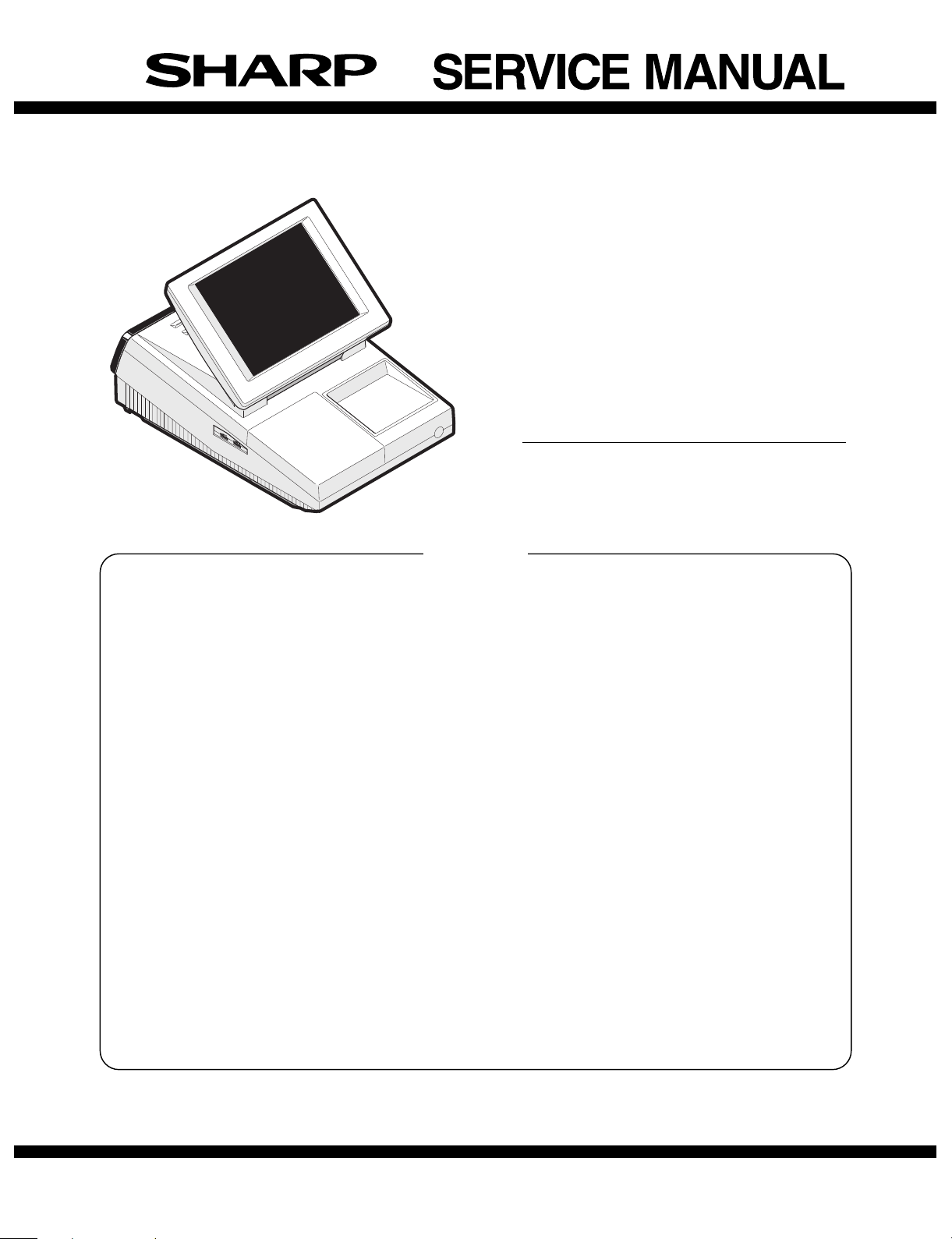
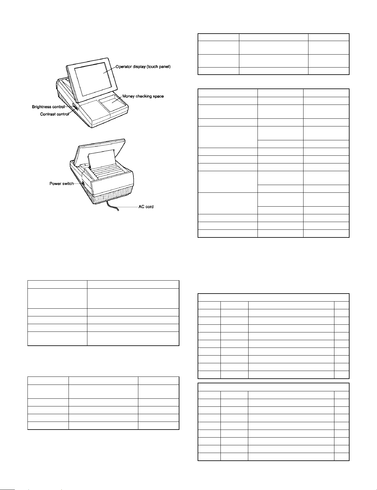
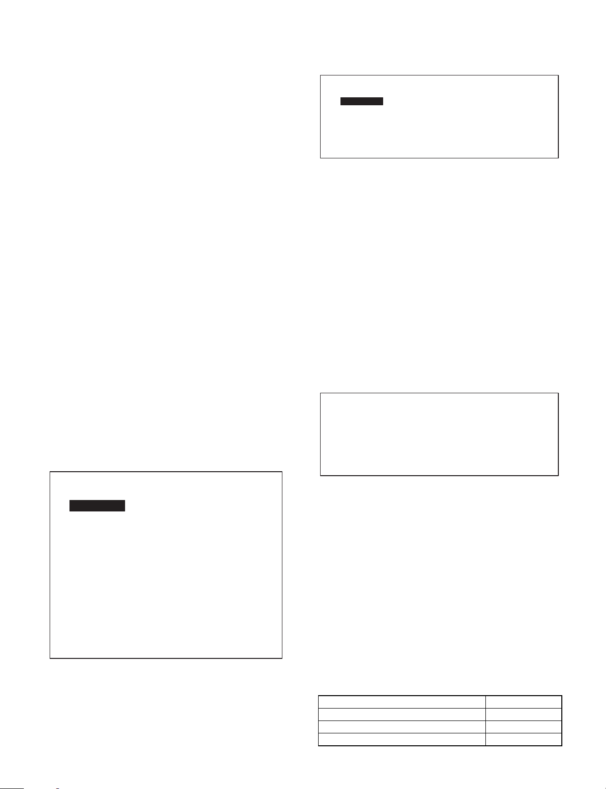
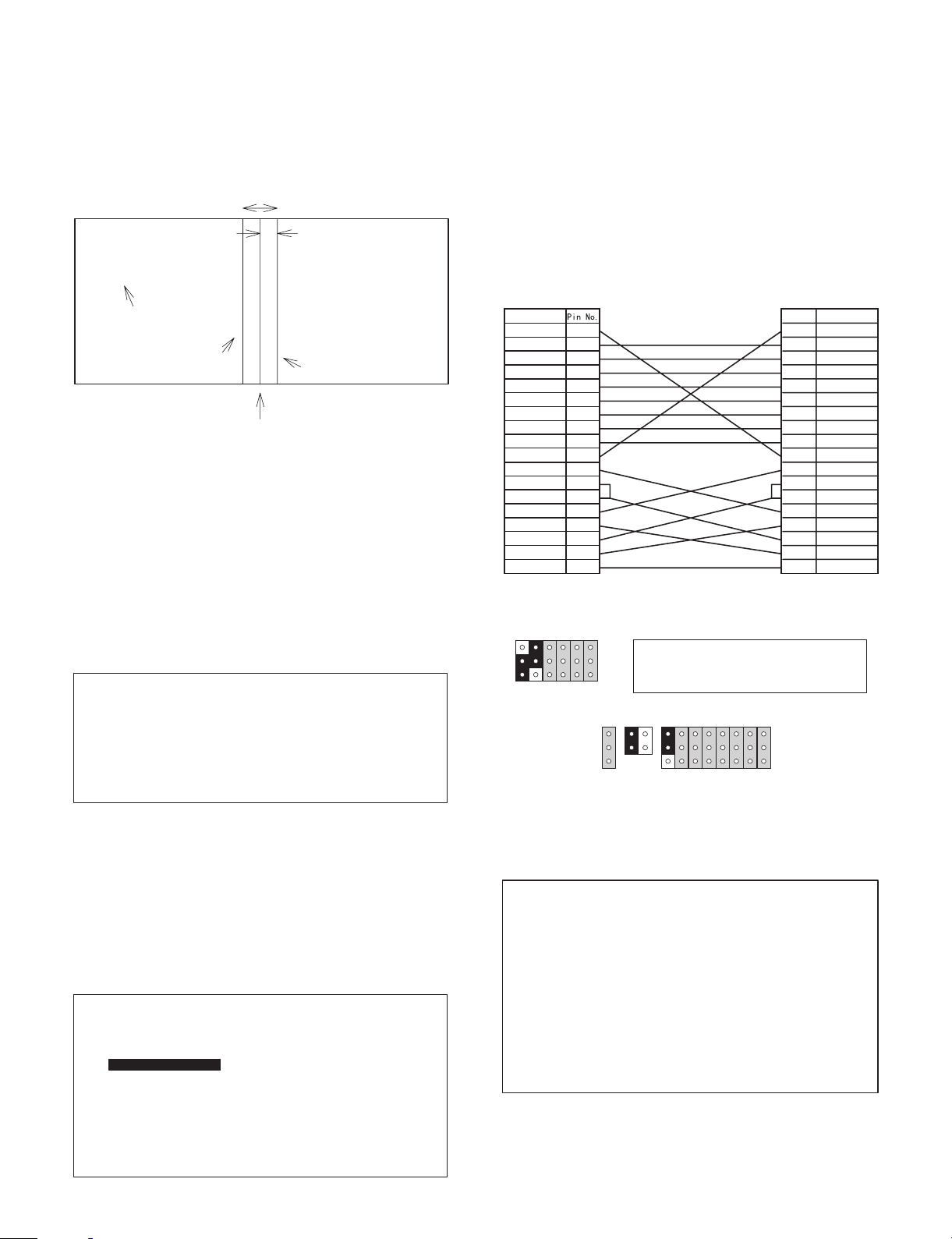
1. Appearance
AC cord
Plug your POS terminal into a wall outlet before using.
Power switch
Set the power switch to the ON ( I ) position after plugging your POS
terminal.
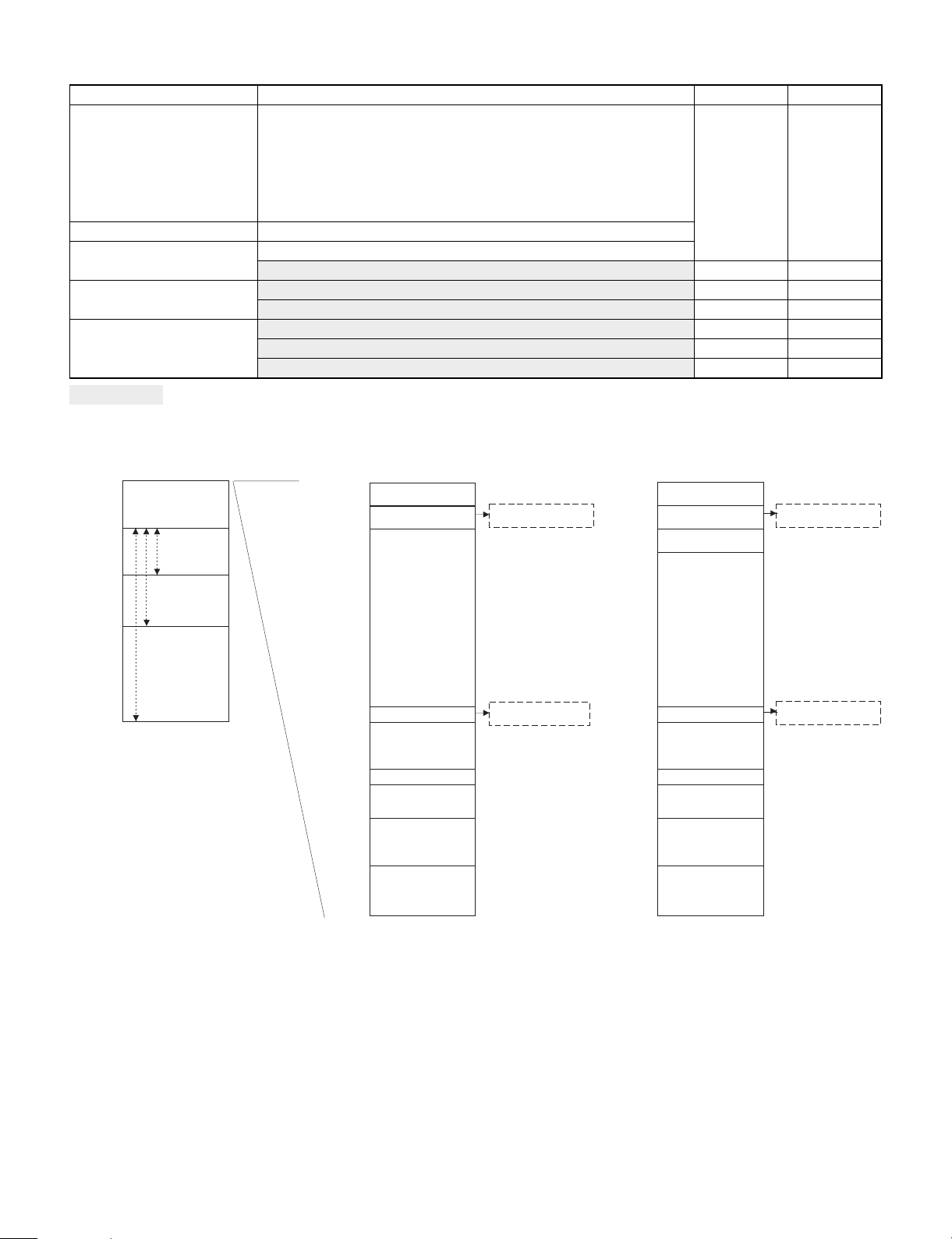
2. Ra tin g
ITEM SPECIFICATIONS
External dimensions 11.6 (W) × 16.3 (D) × 12.6 (H) in.
approximately (295 (W) × 414.5 (D) ×
320 (H) mm)
Weight Approximately 13.9 lb. (5.9 kg)
Power source 120V AC ± 10%, 60 Hz
Power consumption Operating : 63W
Working temperature
and humidity
3. Hardware
3-1. Display
ITEM SPECIFICATIONS NOTE
Type DSTN color LCD with back
Screen size 10.4" Full screen
Dot format 640 (W) × 480 (H) dots
Dot size 0.33 × 0.33 mm
Control VGA
32 to 104°F (0 to 40°C)
10 to 90%
With 256 colors
light
3-2. Keyboard
ITEM SPECIFICATIONS NOTE
Type Touch key
(Analog touch panel)
Number of key
positions
Control Mouse emulation
4096 (W) × 4096 (H)
positions
3-3. PC system
ITEM SPECIFICATIONS NOTE
CPU Pentium processor
Chip set FireStar Plus:
82C700U3.2
Graphic controller VGAC : MN89305
Main memory
(for executing MS-DOS,
Application software)
Video RAM 1 Mbytes EDO type
BIOS ROM 512 Kbytes Flash ROM
OS (MS-DOS) ROM 4 Mbytes Mask ROM
ROM disk memory
(for stored Application
software)
RAM disk memory
(for POS data)
Keyboard controller M38802M270
Super I/O M5113 A2
POS system controller PSC2 : LZ9AM22
Standard : 8
Mbytes
Max. : 40 Mbytes adding S.O.DIMM
Standard : 2
Mbytes
Max. : 6 Mbytes adding UP-F04RB
Standard : 1
Mbytes
Max. : 3 Mbytes adding UP-P02MB
EDO type
Flash ROM
PS-RAM
3-4. Serial port
D-SUB 9-pin connector COM1 and COM2 are equipped.
In order to supply +5V power, CI signal and +5V power supply of
COM1 and COM2 can be switched.
2 channels of RJ45 Connector COM port are equipped.
COM3 and COM4 or original I/O address (COM5 and COM6) can be
selected as the 2 channels of RJ45 COM port.
COM1 & COM2: D-sub 9 pin
Pin No. Signal Function I/O
1 CD Data Carrier Detect I
2 RD Receive Data I
3 SD Send Data O
4 ER Data Terminal Ready O
5 SG Signal Ground —
6 DR Data set Ready I
7 RS Request to Send O
8 CS Clear to Send I
9 CI/+5V Ring Indicate / +5V I/–
COM3 or COM5: Modular jack RJ45 8 pin
Pin No. Signal Function I/O
1 RS Request to Send O
2 ER Data terminal Ready I
3 SD Send Data O
4 SG/(+5V) Signal Ground/(+5V) —
5 SG Signal Ground –
6 RD Receive Data I
7 DR Data set Ready I
8 CS Clear to Send I
1 – 1
Page 4
COM4 or COM6: Modular jack RJ45 8 pin
Pin No. Signal Function I/O
1 RS Request to Send O
2 ER Data terminal Ready I
3 SD Send Data O
4 SG Signal Ground —
5 SG Signal Ground –
6 RD Receive Data I
7 DR Data set Ready I
8 CS Clear to Send I
3-5. Expansion slot
ITEM SPECIFICATIONS NOTE
Type ISA bus Half size PC board
Number of slots 2 slots
Power consumption +5V/max. 1.0A
+12V/max. 0.05A
3-6. Shutdown switch
The shutdown switch is used when the OS or application programs
are straying and the system can not return to the normal state.
You must not use this shutdown switch when the UP-5300 is running
normally. Use this switch only when the main power source is not cut
off even if the main unit power switch is set to OFF position. UP-5300
is turned OFF and the hardware is reset by turning the main power
switch OFF and then pressing the shutdown switch.
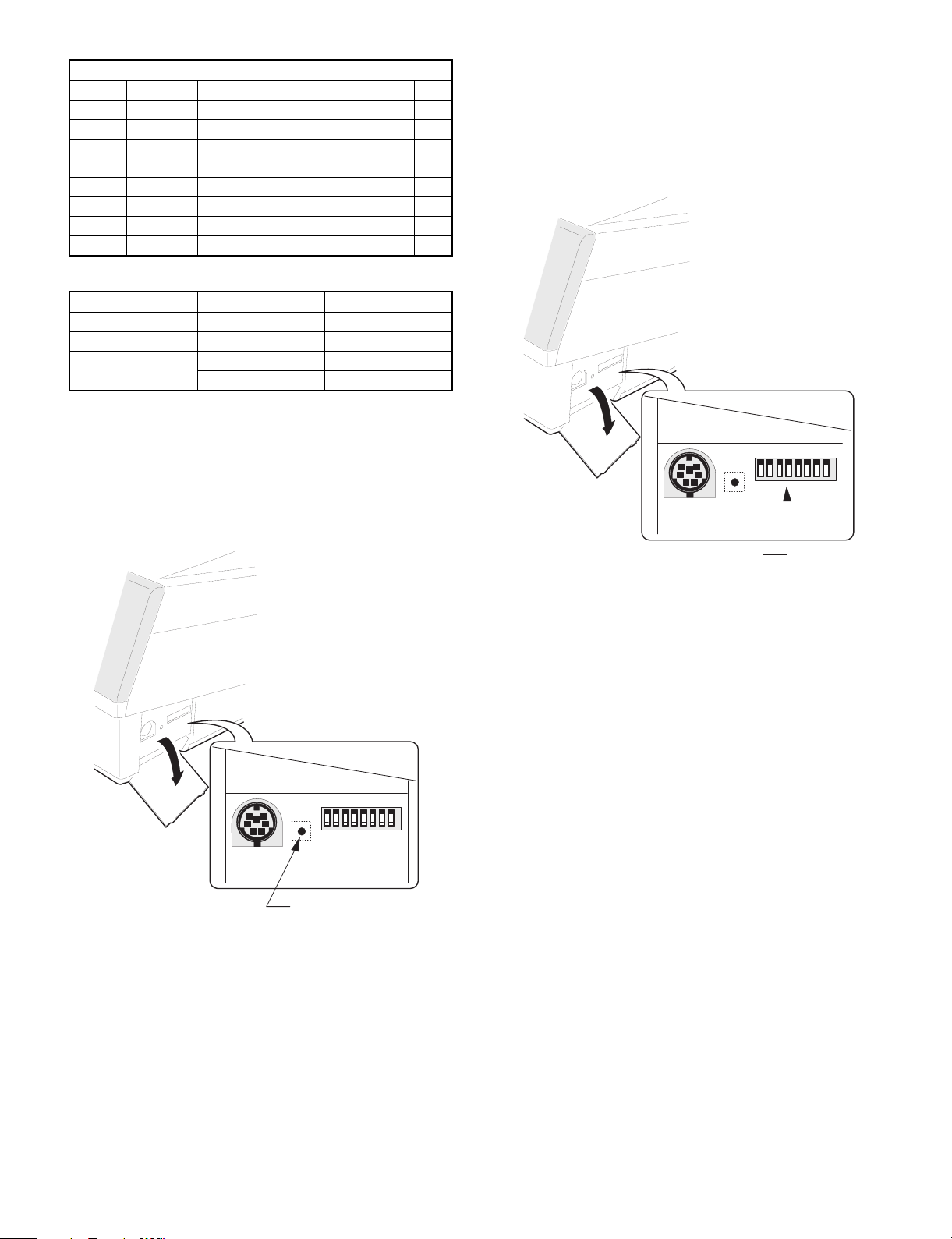
3-7. System switch
The system switches are used to preset various system configurations.
[Out line]
The system switches consists of DIP switches.
[DIP switch]
12345678
12345678
Shut dow n switch
[Out line]
The shutdown switch is single shot type. (Normally OFF position)
Push ON: This position is used to reset stand-by mode for power
supply unit when software hang up.
Release OFF: Usually the shutdown switch needs to be set to this
position when the UP-5300 is operated.
[Operating method]
The shutdown switch is a push switch. If it is pushed to ON, the
UP-5300 stops supplying the power when the power switch is set into
stand-by mode.
NOTE: The shutdown operation will be ignored when te power
switch is set into power-on position.
System sw itch
The PSC2 simply reads the switched signals from the DIP switch as
hardware. The meaning of the switche settings are shown on the next
page.
1 – 2
Page 5
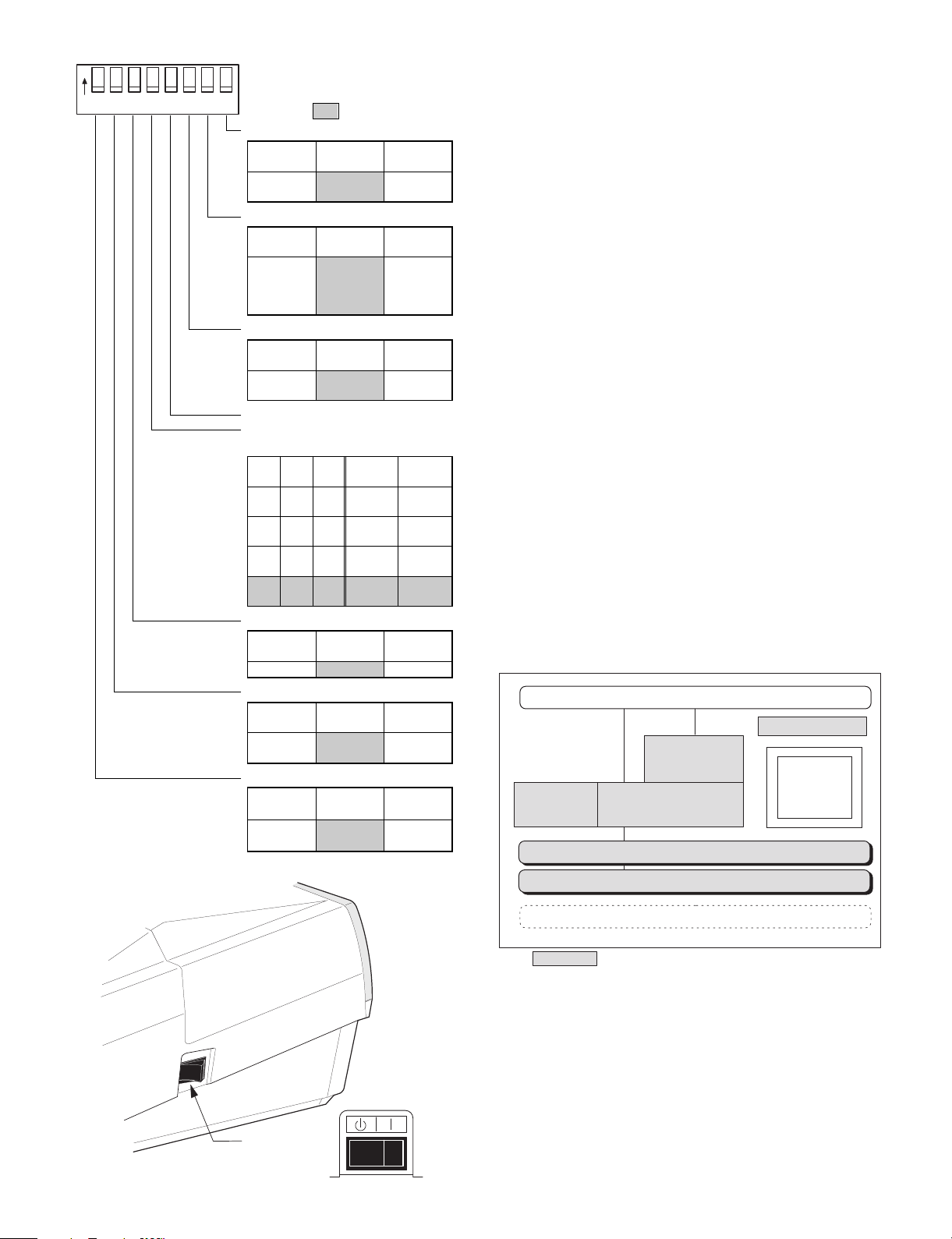
ON
1234567 8
3-8. Power switch
ON
OFF
: De fau lt settin g
DSW-8
Function
Serial 3 & 4
decode mode
OFF
(value=1)
COM3 &
COM4
ON (value=0)
DSW-7
Function
COM3 &
COM4 IRQ
assign
(Serial 3 & 4)
OFF
(value=1)
COM3 =
IRQ11
COM4 =
IRQ10
ON (value=0)
DSW-6
Function
CMOS
Initialize
OFF
(value=1)
Not Initialize Initialize
ON (value=0)
DSW-5
DSW-4
Drive C:, D: & E: Setting
DriveC:DriveD:Drive
HDD — —
PS
HDD
RAM
PS
Flash
RAM
ROM
Flash
ROMPSRAM
DSW-4 DSW-5
E:
ON
(value=0)ON(value=0)
Flash
ROMON(value=0)
OFF
HDD
(value=1)ON(value=0)
OFF
HDD
(value=1)
DSW-3
Function
Boot Drive Drive A: Drive C:
OFF
(value=1)
ON (value=0)
DSW-2
Function
Drive A:
Device
OFF
(value=1)
Mask ROM FDD
ON (value=0)
DSW-1
Function
Floppy Disk
Controller
OFF
(value=1)
Not Exit Exit
ON (value=0)
COM5 &
COM6
COM3 =
IRQ4
COM4 =
IRQ3
OFF
(value=1)
OFF
(value=1)
[Out line]
The power switch has the positions ON and OFF (Stand-by)
ON position: Usually the power switch needs to be set to this posi-
tion when the POS-terminal is operated.
OFF position: This position is used to turn the stand-by mode. When
the power switch is set to this position, the power
supply stops automatically. But if the software program controls the power supply to hold, even if the
power switch is set into this position, power is supplied
until an software program allows power supply no to
hold.
[Operating method]
The power switch is a see-saw switch, and it can be tipped toward
the ON or OFF.
4. Software
4-1. Software Structure
The basic system software mainly consists of the following 3
modules.
(1) MS-DOS Version 6.22
The operating system (MS-DOS Version 6.22) is stored in a MROM
disk.
(2) Drivers
There are following types of drivers
• POS Device Drivers (for Clerk, Buzzer, Drawer, Timer, MCR, Line
Display, Serial Port) POS device drivers adopt the same control
method as previous (ER-A850/A880/UP-5700) softwares.
• Touch Panel Driver
(3) POS Device Middleware
The middleware has been developed to improve the performance of
applications.
(4) Software Structure
Application
POS Utillty
POS Device
Touch
Panel
Driver
Mifddle Wsre
POS Devlce Driver
MS-DOS Version 6.22
BIOS
Standard PC
Device Driver
(Local production)
SCSI
Ethernet
.......etc
Power switch :
Hardware
Provided from SHARP Corporation
1 – 3
Page 6
4-2. Basic system software list
ITEM CONTENTS for UP-5300 for PC
BIOS (FROM) • AT compatible system BIOS
• VGA BIOS for MN89305 VGA LSI
• Standard SETUP program
• Flash Disk/MROM Disk/PSRAM Disk built-in control program
F —
• Memory size/HDD type auto detect function
• No APM/PnP support
OS (MROM disk) MS-DOS Version 6.22 (Subset)
Install program (MROM disk) • System Install program
• APL Install program (for MS-DOS/Windows 95/98/NT) — F
POS device driver • POS device driver F —
• Touch panel driver (mouse emulation I/F only) F —
Middleware software and
application development tools
• POS device MiddleWare F —
• Printer Logo image loading utility program (MS-DOS/Windows 95) FF
• Touch panel calibration utility program (MS-DOS) F —
... These software are provided with FD from SHARP corporation.
Please copy contents of FD provided from department to development PC. Install to UP-5300 by using APL Install Program from PC.
4-3. Memory map
0000000h
STD. 8MB
0800000h
+8MB
1000000h
1800000h
2800000h
(16MB)
+8MB
(24MB)
+32MB
(40MB)
Memory is expandable up to
40MB max. using EMM386 in DOS
00000h
9F4000h
A0000h
C0000h
C8000h
E8000h
100000h
MS-DOS
(25K)
Sharp Driver
(32K)
Free
Conventional
(580K)
EBDA : 3K
VRAM
128K
VGA BIOS(32K)
UMB
(124K)
System BIOS
(96k)
HMA
64K
Middleware Not used
POS Device 20K
Touch Key 12k
(External BIOS
Data Area)
00000h
9F4000h
A0000h
C0000h
C8000h
E8000h
100000h
MS-DOS
(25K)
Sharp Driver
(32K)
Middleware
(15K)
Free
Conventional
(565K)
EBDA:3K
VRAM
128K
VGA BIOS(32K)
UMB
(124K)
System BIOS
(96k)
HMA
64K
Middleware is used
POS Device 20K
Touch Key 12k
(External BIOS
Data Area)
1 – 4
Page 7
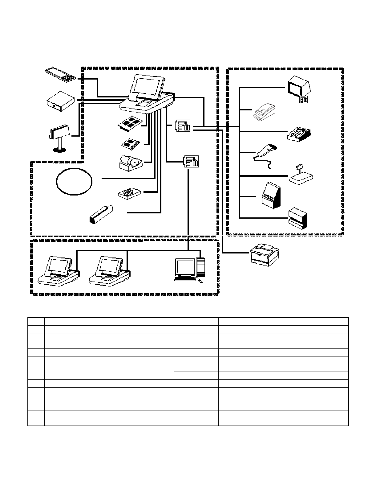
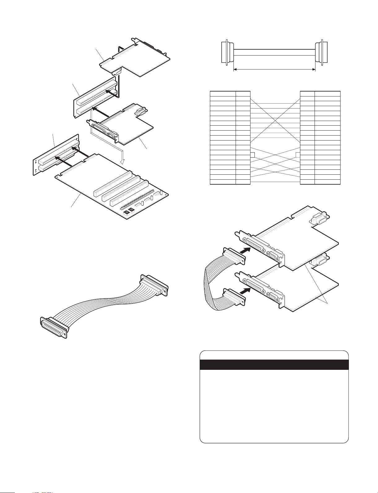
CHAPTER 2. OPTIONS
1. System configuration
Incorporated in Main Unit RS-232 Communication Connection
AT Keyboard
<supplied on site>
max.2
Drawer
<Option>
ER-03DW/
04W/05DW
(In Europe only)
Customer
Poll Display
<Option>
UP-P20DP
Built-in,
customer-side
display
<Option>
UP-I20DP
(NEW)
Additional
RAM Memory
<Option>
UP-P02MB
Additional
ROM Memory
<Option>
UP-F04RB
Additional DRAM
Memory
<supplied on site>
Built-in printer
<Option>
UP-T80BP
HDD Unit
<supplied on site>
UP-5300
(RS-232)
(Standard 4 channels)
(Additional 2 channels)
RS232 Board
<Option>
ER-A8RS
Ethernet Board
<supplied on site>
Kitchen video monitor
<supplied on site>
(For North America only)
Remote Printer
<Option> ER-01PU
<supplied on site>
Hand Scanner
<Option>
ER-A6HS1
Coin dispenser
<supplied on site>
(For North America only)
TM-T80/85/295
ER-FBT40
<supplied on site>
<supplied on site>
CAT/FET
Scale
Magnetic
Card Reader
<Option>
UP-E12MR
In-line Communication
Connection
UP-5300
Host PC
PC
<supplied on site>
Centronics Printer
<supplied on site>
2. Options
No. NAME MODEL NAME DESCRRIPTION
1 Expansion RAM disk board UP-P02MB 2 Mbytes RAM board
2 Expansion ROM disk board UP-F04RB 4 Mbytes ROM board
3 Customer display UP-I20DP 2 line 20 digits dot display
4 Customer pole display UP-P20DP 2 line 20 digits dot display
5 MCR (Magnetic Card Reader) UP-E12MR2 for ISO 1 & 2 stripe card
6 Remote drawer ER-03DW 7B/5C
ER-04DW 5B/5C
7 Receipt/Journal printer ER-01PU 2 station (R/J) thermal printer 45mm width
8 Built-in printer UP-T80BP 1 station thermal printer 80mm width
9 RS232 & CENTRO I/F board ER-A8RS RS232 9 pins connector:2 ports
Centronics 25 pins connector : 1 port
10 Hand scanner ER-A6HS1 for reading bar code
11 FDD unit HZ-H14FD 3.5" Floppy Disk Drive (Newtronics D353M3)
Drink dispenser
<supplied on site>
(For Europe only)
2 – 1
Page 8
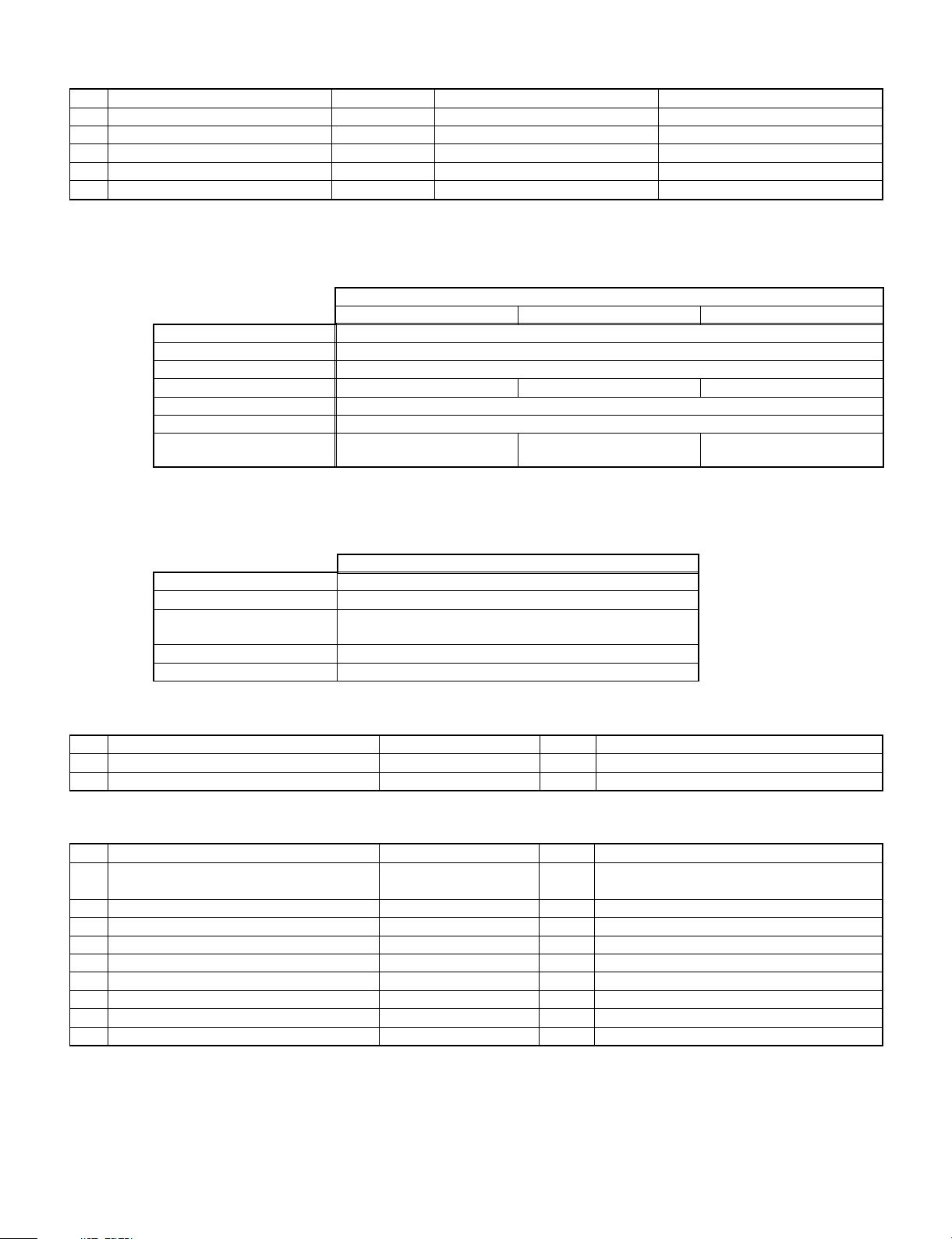
3. Locally supplied options
No. NAME MODEL NAME DESCRIPTION
1 S.O.DIMM Small Outline DIMM Max. 32Mbyte *1
2 HDD (by FUJITSU) MHD2021AT 2.5 inch, 2.1Gbyte *2
3 PC keyboard PS/2 type PC keyboard
4 Application software
5 Additional device drivers
*1 EXTENSION RAM MODULE (Provided through SHARP Electronics Corporation)
[Outline] UP-5300 has a socket as Small Outline DIMM.
It is necessary to satisfy with S.O.DIMM memory specification as follows.
[Specification]
144pin S.O.DIMM
8 Mbytes 16 Mbytes 32 Mbytes
TYPE EDO type
ACCESS TIME 60 nsec. (less than)
POWER 3.3 V
REFRESH CYCLE 1024/16 msec. 2048/32 msec. 4096/64 msec.
REFRESH TYPE CBR
POWER CONSUMPTION 700 mA (less than)
OTHER 4 chip × 16 Mbits
*2 HARD DISK DRIVE (Local purchase)
[Outline] UP-5300 may be connected to the Hard Disk Drive.
[Specification]
It is necessary to satisfy the 2.5 inch Hard Disk Drive specification as follows.
MAKER FUJITSU
MODEL MHD2021AT
PARTS No.
REVISION No.
CAPACITY 2.16 Gbytes
INTERFACE ATA-3
1) Part No.: CA 01640-B040
Rev. No.: A4
(1 Mwords × 16 bits)
2.5 inch type Hard Disk Drive
8 chip × 16 Mbits
(2 Mwords × 8 bits)
4 chip × 64 Mbits
(4 Mwords × 16 bits)
4. Service options
No. NAME PARTS CODE PRICE DESCRIPTION
1 Connector cable for Dongle (LPT-1) QCNW-7858BHZZ BL Relay line from Terminal to Dongle
2 HDD mounting kit DKIT-8671RCZZ — Bracked assembly for mounting
5. Service tools
No. NAME PARTS CODE PRICE DESCRIPTION
1 Service tool kit DKIT-8656BHZZ CW ISA checker
ISA relay board
2 Printer connector signal loop back connector UKOG-6717RCZZ BR for ER-A8RS CENTRONICS connector
3 MCR test card UKOG-6718RCZZ BE for UP-E12MR
4 RS232 loop back connector UKOG-6705RCZZ BC for RS232 connector
5 CPU/VGA PWB relay PWB CKOG-6728BHZZ CQ
6 BIOS loading board CKOG-6727BHZZ CS for overwriting BIOS
7 RS232 modular jack loop back connector UKOG-6729BHZZ AZ for RJ45 connector
8 BIOS MASTER ROM VHI27040RBQ1A (P) EP-ROM for overwriting BIOS
9 TOUCH PEN CPENP1004PCN5 AG
2 – 2
Page 9
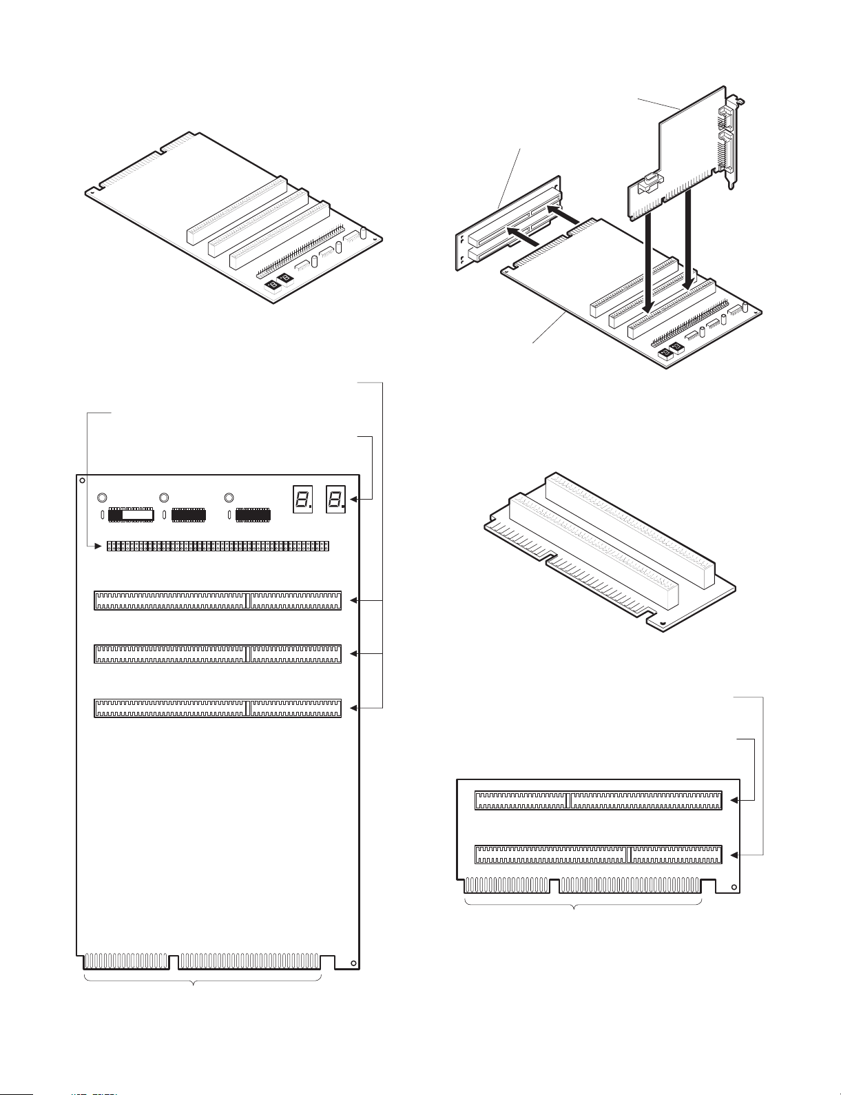
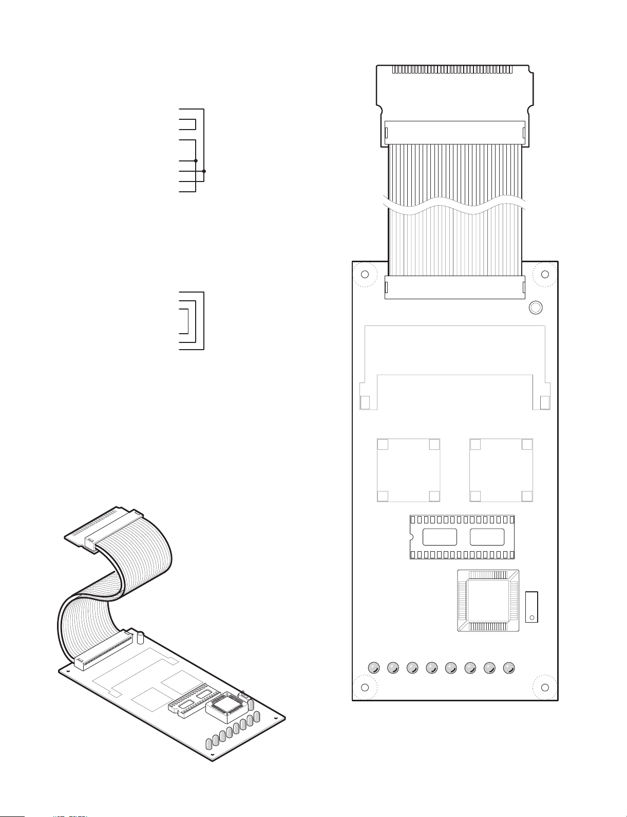
4-1. Service tool kit: DKIT-8656BHZZ
1) ISA checker
Used to repair or check the operation of the optional I/F.
• External view
• Plain view
ISA bus connectors:
Used to connect with the I/F PWB of ER-A8RS etc.
Test pins: Used to check the ISA bus signal.
LED circuit: Not used currently.
• Connection diagram
ER-A8RS
UP-5300
ISA bus connector
ISA checker
2) ISA relay board
Connected to the ISA checker for installation of the optional I/F
horizontally and for repairing and checking the operation .
• External view
RAM1A
• Plain view
ISA bus connector:
Used to check the ER-A8RS parts side.
ISA bus connector:
Used to check the ER-A8RS solder side.
Connected to the UP-5300 ISA bus connectors.
Connected to the ISA bus connector of ISA checker.
2 – 3
Page 10
• Connection diagram
ER-A8RS solder side
ISA relay board
• Plan view and connection diagram
150±8
ISA PWB
ER-A8RS parts side
ISA checker
4-2. Printer connector signal loop check cable:
UKOG-6717RCZZ
Connected to the centronics connector (25 pin) of the ER-A8RS, and
is used to check loop signals when executing diagnostics.
• External view
Signal name Pin No.
1STROBE2DB0
3DB1
4DB2
5DB3
6DB4
7DB5
8DB6
9DB7
10ACK11BUSY
12PE
13SLCT
14AUTOFD15ERROR16INIT17SLCTIN-
18~25PE
• Connection diagram
Signal namePin No.
1 STROBE2 DB0
3 DB1
4 DB2
5 DB3
6 DB4
7 DB5
8 DB6
9 DB7
10 ACK11 BUSY
12 PE
13 SLCT
14 AUTOFD15 ERROR16 INIT17 SLCTIN-
18~25 PE
4-3. MCR test card: UKOG-6718RCZZ
• Used when executing the diagnostics of the UP-E12MR2.
• External view
2 – 4
ER-A8RS
Page 11
4-4. RS232 loop back connector: UKOG-6705RCZZ
Connected to the RS232 connector (D-SUB 9 pin: COM1, COM2,
COM3, COM4) of the UP-5300 and ER-A8RS, and used to check
loop signals when executing diagnostics.
• Connection diagram
CD 1pin
RD 2pin
TD 3pin
DTR 4pin
GND 5pin
DSR 6pin
RTS 7pin
CTS 8pin
RI 9pin
4-5. RS232 modular jack loop back connector:
UKOG-6729BHZZ
Connected to the RS232 connector (RJ45: COM3, COM4, COM5,
COM6) of the UP-5300, and used to check loop signals when executing diagnostics.
• Connection diagram
1pin
RTS
2pin
DTR
3pin
TD
4pin
GND
5pin
GND
6pin
RD
7pin
DSR
8pin
CTS
• Plain view
4-6. BIOS loading board: CKOG-6727BHZZ
The BIOS loading board: CKOG-6727BHZZ is a tool to write a BIOS
ROM program in the F-ROM on the UP-5300’s main board. Use this
PWB in the following cases:
• The F-ROM on the UP-5300’s main board be comes unreadible
and a BIOS ROM program must be written in the F-ROM.
• The BIOS ROM program in the F-ROM is overwritten due to the
version up of BIOS ROM program, etc.
The BIOS loading board is connected to the Option ROM/RAM disk
connector (CN5) of the Main PWB.
• External view
SW1
13
• Connection diagram
2 – 5
LED1 LED2 LED3 LED4 LED5 LED6 LED7 LED8
Page 12
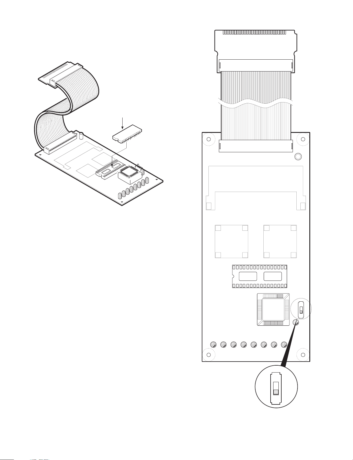
Writing BIOS ROM Program
NOTE: Remove all option boards from the ISA slots before writing
on the BIOS ROM.
1. Install the EP-ROM (master ROM): containing a BIOS program on
the BIOS loading board: CKOG-6727RCZZ.
BIOS MASTER ROM
2. Set SW1 on the BIOS loading board to the side of pin 3.
* Caution: The AC power must be removed prior to installing the
BIOS loading board.
LED1 LED2 LED3 LED4 LED5 LED6 LED7 LED8
SW1
SW1
1
3
LED9
SW1
1
2 – 6
3
Page 13
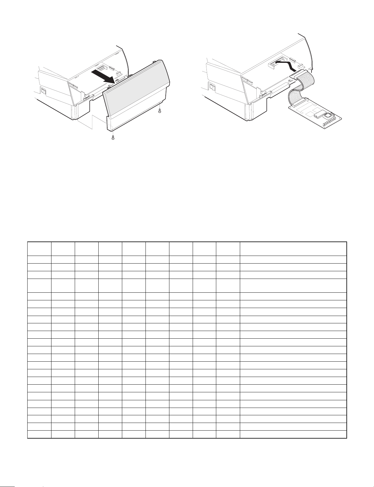
3. Open the upper cabinet.
4. Connect the BIOS loading board to the option ROM/RAM connector CN5 on the main PWB, and then close the cabinet.
5. Writing the BIOS ROM program starts by turning on the power
switch on the right side.
To determine the status of the LED lights on the special service
PWB when a BIOS ROM program is being written, see the table
on the next page.
Writing is complete (automatic completion) when the green LED
(LED9) on the BIOS loading board lights up.
6. After writing is complete, turn off the power switch on the right side
to remove the BIOS loading board, and turn on the power switch
on the left side again to check whether the BIOS program starts
up normally or not.
LED DISPLAY STATUS
[E : ON (Lighting) — : OFF]
<In normal operation>
LED1
(RED)
EEEEEEEE— Start of COPY FUNCTION
————E ————Start initializing
—————E — — — Erasing F-ROM (LED6: RED is blinking)
————EE———
————EE— — — Programming: Bank0 C0000 h (64KB)
E ———EE— — — Programming: Bank0 D0000 h (64KB)
— E ——EE— — — Programming: Bank0 E0000 h (64KB)
EE——EE— — — Programming: Bank0 F0000 h (64KB)
———EEE— — — Programming: Bank1 C0000 h (64KB)
E ——EEE— — — Programming: Bank1 D0000 h (64KB)
— E — EE E— — — Programming: Bank1 E0000 h (64KB)
EE— EEE— — — Programming: Bank1 F0000 h (64KB)
——————E — — Start verifying the program in the F-ROM
——————E — — Verifying: Bank0 C0000 h (64KB)
E —————E — — Verifying: Bank0 D0000 h (64KB)
— E ————E — — Verifying: Bank0 E0000 h (64KB)
EE————E — — Verifying: Bank0 F0000 h (64KB)
———E ——E — — Verifying: Bank1 C0000 h (64KB)
E ——E ——E — — Verifying: Bank1 D0000 h (64KB)
— E — E ——E — — Verifying: Bank1 E0000 h (64KB)
EE— E ——E — — Verifying: Bank1 F0000 h (64KB)
————E — E — — Setting protection the F-ROM
EEEEEEEEEEND of complete COPY FUNCTION
LED2
(RED)
LED3
(RED)
LED4
(RED)
LED5
(RED)
LED6
(RED)
LED7
(RED)
LED8
(RED)
LED9
(GREEN)
FUNCTION
Start copy programming to F-ROM from EPROM
2 – 7
Page 14
<Erase ERROR in F-ROM>
LED1
(RED)
E ————E — E — Device not ready
— E ——— E — E — VPP error
EE———E — E — Command sequence error
——E —— E — E —
<Programming ERROR in F-ROM>
LED1
(RED)
E ———EE— E — Device not ready
— E ——EE— E — VPP error
EE——EE— E — Command sequence error
<Verifying ERROR in F-ROM>
LED1
(RED)
E ———E — EE— Device not ready while release the protection
— E ——E — EE— Can not release the protection
LED2
(RED)
LED2
(RED)
LED2
(RED)
LED3
(RED)
LED3
(RED)
LED3
(RED)
LED4
(RED)
LED4
(RED)
LED4
(RED)
LED5
(RED)
LED5
(RED)
LED5
(RED)
LED6
(RED)
LED6
(RED)
LED6
(RED)
LED7
(RED)
LED7
(RED)
LED7
(RED)
LED8
(RED)
LED8
(RED)
LED8
(RED)
LED9
(GREEN)
LED9
(GREEN)
LED9
(GREEN)
FUNCTION
FUNCTION
FUNCTION
2 – 8
Page 15
CHAPTER 3. SERVICE PRECAUTION
1. Conditions for soldering circuit parts
To solder the following parts manually, follow the conditions described below.
PARTS NAME PARTS CODE LOCATION CONDITIONS FOR SOLDERING
Ceramic oscillator RCRMZ7002RCZZ TOCH PANEL CONTROL
PWB: X1 (8M)
RCRMZ7003RCZZ MAIN PWB: X2 (24M)
RCRMZ7004RCZZ MAIN PWB: X2 (7.37M)
DIP SWITCH QSW-Z7011XCZZ SWITCH PWB: S2 300°C/3sec.
270°C/3sec.
2. Cautions on handling CPU and POWER
FAN
When removing or performing maintenance activities on the CPU and
POWER FAN, be sure to handle them with care, because it may
cause abnormal sounds or deteriorate their performance if they are
dropped or exposed to a heavy impact.
3. Note for handling of Touch panel
• The transparency of the touch panel should be vitally important.
Use clean gloves and masks.
• For handling, do not hold the transparent area, and do not hold the
heat seal connector section to assure reliability.
• Do not overlay touch panels. The edge may damage the surface.
• Do not place heavy things on the touch panel.
• Do not apply a strong shock, and do not drop it.
• When attaching the protection film again, carefully check for dirt. If
there is any dirt, it is transferred.
• To clean dirt on the surface, use a dry, soft cloth or a cloth im -
mersed in ethyl alcohol.
• Check that the housing does not give stress to the touch panel.
• Be careful not to touch the touch panel with tools.
• The heat seal section is easily disconnected. Be careful not to
place stress to the heat seal section when installing.
• The touch panel is provided with an air groove to make the exter -
nal and the internal air pressure equal to each other. If water or oil
is put around the air groove, it may penetrate inside. Be careful to
keep the air groove away from water and oil.
• Do not use SHARP objects when making input entrres.
4. Note for handling of LCD
• The LCD elements are made of glass. BE careful not to expose
them strong mechanical shock, or they may be broken. Use extreme care not to break them.
• If the LCD element is broken and the liquid leaks, avoid contact
with your mouth or eyes. If the liquid comes in contact with your
skin or clothes, immediately clean with soap.
• Use the unit under the rated conditions to prevent against damage.
• Be careful not to place water or other liquids on the display sur -
face.
• The reflection plate and the polarizing plate are easily scratched.
BE careful not to touch them with a hard object such as glass,
tweezers etc. Never hit, push, or rub the surface with hard objects.
• When installing the unit, be careful not to apply stress to the LCD
module. If excessive stress is applied, abnormal display or uneven
color may result.
5. Cautions on handling connectors
When connecting or disconnecting the following connectors, follow
the procedures below.
1)
PARTS NAME PARTS CODE LOCATION
FFC
CONNECTOR
• How to insert FFC
(1) Pull the slider to the unlock position.
QCNCW2812BH3J LCD RELAY
PWB: CN8
3 – 1
Page 16
(2) Open the slider upwards.
(3) Inserting the FFC
Insert the FFC firmly until the FFC hits the bottom of the
connector’s insulator.
FFC
FFC FFC FFC
CONNECTOR CONNECTOR CONNECTOR
(4) Close the slider to the lock position
FFC
FFC
6. AT Keyboard usable for UP-5300
The UP-5300 can be externally connected to a keyboard.
The UP-5300’s key BIOS conforms to the PC standard, but this
BIOS’s operation is not compatible for some keyboards.
Some keyboards may cause operation errors due to delicate timing
and conflicts.
It is currently found that the following models of keyboards may malfunction.
When selecting a keyboard to be connected, test the keyboard in
advance to check that it correctly works.
• Japanese keyboard (106 keys)
Manufactured by IBM: TYPE/MODEL5576-B01 FRUPN66G0507
• English keyboard (101 keys)
Manufactured by NMB Technologies Inc.: Model: RT6651T+
3 – 2
Page 17
CHAPTER 4. UP-5300 DIAGNOSTICS
SPECIFICATIONS
CONTENT
1. General . . . . . . . . . . . . . . . . . . . . . . . . . . . . . . . . . . . . . . . . . . 4-2
2. System configuration . . . . . . . . . . . . . . . . . . . . . . . . . . . . . . . . 4-2
3. Service diagnostics . . . . . . . . . . . . . . . . . . . . . . . . . . . . . . . . . 4-2
3-1. Service diagnostics getting started . . . . . . . . . . . . . . . . 4-2
3-2. Selection menu . . . . . . . . . . . . . . . . . . . . . . . . . . . . . . . 4-2
3-3. RAM Diagnostics . . . . . . . . . . . . . . . . . . . . . . . . . . . . . . 4-2
1) D-RAM Check . . . . . . . . . . . . . . . . . . . . . . . . . . . . 4-2
2) Standard RAM Disk Check . . . . . . . . . . . . . . . . . . . 4-2
3) OPTION RAM Disk Check . . . . . . . . . . . . . . . . . . . 4-3
3-4. ROM Diagnostics . . . . . . . . . . . . . . . . . . . . . . . . . . . . . 4-3
1) DOS ROM Check . . . . . . . . . . . . . . . . . . . . . . . . . . 4-3
2) BIOS ROM Check . . . . . . . . . . . . . . . . . . . . . . . . . 4-3
3) Standard FLASH ROM Check . . . . . . . . . . . . . . . . 4-4
4) Option FLASH ROM Check . . . . . . . . . . . . . . . . . . 4-4
3-5. Real time clock & CMOS RAM Diagnostics . . . . . . . . . 4-4
1) Real time clock Check . . . . . . . . . . . . . . . . . . . . . . 4-5
2) CMOS RAM Check . . . . . . . . . . . . . . . . . . . . . . . . 4-5
3-6. Touch Panel Diagnostics . . . . . . . . . . . . . . . . . . . . . . . 4-5
1) Controller Diag Test . . . . . . . . . . . . . . . . . . . . . . . . 4-5
2) Touch Key Pad Test . . . . . . . . . . . . . . . . . . . . . . . . 4-5
3) Linearity Test . . . . . . . . . . . . . . . . . . . . . . . . . . . . . 4-6
3-7. Clerk Key Diagnostics . . . . . . . . . . . . . . . . . . . . . . . . . . 4-6
1) Clerk Key Check . . . . . . . . . . . . . . . . . . . . . . . . . . . 4-6
3-8. Printer Diagnostics . . . . . . . . . . . . . . . . . . . . . . . . . . . . 4-6
1) PARALLEL1 Loop Check . . . . . . . . . . . . . . . . . . . . 4-6
2) PARALLEL2 Loop Check . . . . . . . . . . . . . . . . . . . . 4-7
3) PARALLEL3 Loop Check . . . . . . . . . . . . . . . . . . . . 4-7
4) PARALLEL1 Print Check . . . . . . . . . . . . . . . . . . . . 4-7
5) PARALLEL2 Print Check . . . . . . . . . . . . . . . . . . . . 4-8
6) PARALLEL3 Print Check . . . . . . . . . . . . . . . . . . . . 4-8
7) UP-T80BP Test . . . . . . . . . . . . . . . . . . . . . . . . . . . 4-8
3-9. Serial I/O Diagnostics . . . . . . . . . . . . . . . . . . . . . . . . . . 4-9
1) COM1 Check . . . . . . . . . . . . . . . . . . . . . . . . . . . . . 4-9
2) COM2 Check . . . . . . . . . . . . . . . . . . . . . . . . . . . . . 4-9
3) COM3 Check . . . . . . . . . . . . . . . . . . . . . . . . . . . . . 4-9
4) COM4 Check . . . . . . . . . . . . . . . . . . . . . . . . . . . . 4-10
5) COM5 Check . . . . . . . . . . . . . . . . . . . . . . . . . . . . 4-10
6) COM6 Check . . . . . . . . . . . . . . . . . . . . . . . . . . . . 4-10
3-10. Liquid Crystal Display Diagnostics . . . . . . . . . . . . . . . 4-10
1) Liquid Crystal Display Check . . . . . . . . . . . . . . . . 4-10
3-13. Magnetic Card Reader Diagnostics . . . . . . . . . . . . . . 4-11
1) Magnetic Card Reader Check . . . . . . . . . . . . . . . 4-11
3-14. System Switch Diagnostics . . . . . . . . . . . . . . . . . . . . . 4-11
1) System Switch . . . . . . . . . . . . . . . . . . . . . . . . . . . 4-11
3-15. Drawer Diagnostics . . . . . . . . . . . . . . . . . . . . . . . . . . . 4-11
1) Drawer 1 Check . . . . . . . . . . . . . . . . . . . . . . . . . . 4-11
2) Drawer 2 Check . . . . . . . . . . . . . . . . . . . . . . . . . . 4-12
3-16. Option Display Diagnostics . . . . . . . . . . . . . . . . . . . . . 4-12
3-17. IDE I/F & HARD DISK Diagnostics . . . . . . . . . . . . . . . 4-12
[READ MODE TEST] . . . . . . . . . . . . . . . . . . . . . . . . . 4-12
1) Drive Status display . . . . . . . . . . . . . . . . . . . . . . . 4-12
2) Sequential Seek Test . . . . . . . . . . . . . . . . . . . . . . 4-12
3) Random Seek Test . . . . . . . . . . . . . . . . . . . . . . . . 4-13
4) Seek&Read Test . . . . . . . . . . . . . . . . . . . . . . . . . 4-13
5) Target Sector Read Test . . . . . . . . . . . . . . . . . . . 4-14
6) HD Dump Test . . . . . . . . . . . . . . . . . . . . . . . . . . . .4-14
7) Error lnformation Display . . . . . . . . . . . . . . . . . . . .4-14
8) Controller check Test . . . . . . . . . . . . . . . . . . . . . . .4-15
[WRITE MODE TEST] . . . . . . . . . . . . . . . . . . . . . . . . .4-15
9) Seek&Write/Read-Verify Test . . . . . . . . . . . . . . . .4-15
10) Target Sector Write/Read-Verify Test . . . . . . . . . .4-16
11) HDPatch Test (Utility) . . . . . . . . . . . . . . . . . . . . . .4-16
12) Error Logging Area Clear . . . . . . . . . . . . . . . . . . . .4-16
13) Error table display . . . . . . . . . . . . . . . . . . . . . . . . .4-16
14) Other Supplemental Items . . . . . . . . . . . . . . . . . . .4-16
15) Error Content . . . . . . . . . . . . . . . . . . . . . . . . . . . . .4-16
16) Error Information Storing Area Description . . . . . .4-16
3-18. FDD Diagnostics . . . . . . . . . . . . . . . . . . . . . . . . . . . . . .4-17
3-19. FAN & LCD ON/OFF Diagnostics . . . . . . . . . . . . . . . . .4-17
1) FAN & LCD ON/OFF Check . . . . . . . . . . . . . . . . .4-17
3-20. Power Hold Diagnostics . . . . . . . . . . . . . . . . . . . . . . . .4-17
1) Power Hold Check . . . . . . . . . . . . . . . . . . . . . . . . .4-17
Subsequently the POS application software is added which may overwrite the F-ROM area.
Please check to insure that the diagnostic program is installed along
with the POS application.
Starting Diagnostics when an Application software is
installed:
(1) Execute the diagnostic program by rebooting the UP-5300 from
the BIOS-ROM (MASK ROM).
1) Remove AC power by placing the power switch to the "off"
position.
2) Set the system switches (DSW-2 and DSW-3) as follows:
ON
1234567 8
DSW-3
DSW-2
Drive A: Device Mask ROM FDD
3) Connect the AT keyboard.
4) Turn on the AC power on to start upthe BIOS-ROM (MASK
ROM).
Then the incorporated system installer utility will start.
5) Press the ESC key on the AT keyboard, and select "EXIT"
followed by pressing the ENTER key to exit the System
installer.
The UP-5300 will go to the A:\> prompt.
6) To select the drive that of diagnostics program, type "C:\"
followed by the ENTER key.
7) At the "C:\" prompt , type "SRV" followed by the ENTER key
to start the serviceman’s diagnostic program.
ON
OFF
Function OFF (value = 1) ON (value = 0)
Boot Drive Drive A: Drive C:
Function OFF (value = 1) ON (value = 0)
Starting Diagnostics when an Application software is
installed:
(2) To execute the diagnostic program when an application program
is also installed.
1) Remove AC power by placing the power switch to the "off"
position.
2) Set the system switches (DSW-2 and DSW-3) as shown
above:
3) Connect the AT keyboard.
4) Turn on the AC power.
4 – 1
Page 18
5) Depress the F8 function key located on the AT keyboard and
start the UP-5300 without executing the "CONFIG.SYS" and
the "AUTOEXEC.BAT". The UP-5300 will go to the A:\>
prompt.
6) To select the drive that of diagnostics program, type "C:\"
followed by the ENTER key.
7) At the "C:\" prompt , type "SRV" followed by the ENTER key
to start the serviceman’s diagnostic program.
1. General
This diagnostic program is used to check the PWB’s, the process,
and the machine of UP-5300 series in a simplified manner.
This test program is supplied with floppy disks.
2. System configuration
The system requires the UP-5300, and an AT keyboard for diagnostic
operations.
3. Service diagnostics
3-1. Service diagnostics getting started
Getting started:
Execute "SRV.BAT" by entering the command with the AT keyboard
as follows:
C:\> SRV ↵
"C:\>" is the DOS prompt. (Used by the F-ROM disk based on the
settings of the system switches.)
* Do not load any device drivers when using this program.
* To operate other applications after performing this program, reboot
the machine.
3-2. Selection menu
The diagnostics menu is started and the following menu is displayed.
The highlighted cursor is moved by the cursor keys (UP ↑ and DOWN
↓) of the AT keyboard. Move the cursor to the desired item, and press
the Enter key to execute the selected diagnostics program. When the
selected diagnostics program is completed, the display returns to the
menu screen by pressing the ESC key. Select "Diagnostics End" and
press the Enter key to terminate the diagnostics.
When the selected diagnostics program is completed, Press the ESC
key to return to the RAM menu screen. Pressing the Esc key again
returns to the service diagnostics menu.
RAM Diagnostics
D-RAM Check
Standard RAM Disk Check
Option RAM Disk Check
1) D-RAM Check
1 Checking content
All memory areas are checked in units of 64KB. The checking
procedures are as follows:
i. Test data 5555H is written to all the test areas.
ii. Test data and read data are compared by each word, If it is
O.K., test data AAAAH is written to the test area.
iii. Test data and read data are compared by each word, If it is
O.K., test data 5555H is written to the test area.
iv. Test data 0000H is written to all the test areas.
v. Test data and read data are compared by each word, If it is
O.K., test data FFFFH is written to the test area.
vi. Test data and read data are compared by each word, If it is
O.K., test data 0000H is written to the test area.
When an error occurs during the test, the error address and data
are displayed and the test is stopped.
For the extension memory test, the value set in the setup of read
and test and is made to the area in increments of 64KB.
2 Display
D-RAM Check
Main memory size : 640KB PASS !!(or ERROR !!)
Extended memory size : xxxxKB PASS !!(or ERROR !!)
Error Address xxxxxxH Write Data xxxxH Read Data xxxxH
SHARP PC-POS System Diagnostic Series I
Diagnostics for Service
RAM Diagnostics
ROM Diagnostics
Real time clock & CMOS RAM Diagnostics
Touch Panel Diagnostics
Clerk Key Diagnostics
Printer Diagnostics
Serial I/O Diagnostics
LCD (Liquid Crystal Display) Diagnostics
MCR (Magnetic Card Reader) Diagnostics
System Switch Diagnostics
Drawer Diagnostics
Option Display Diagnostics
IDE I/F & Controller Diagnostics
FDD Diagnostics
FAN&LCD ON/OFF Diagnostics
Power Hold Diagnostic
Diagnostics End
Version 1.00B
3-3. RAM Diagnostics
This program is used to test the standard memory, the extension
memory, and the RAM disk.
When this program is selected, the following menu is displayed.
The highlighted cursor is moved by the cursor keys (UP ↑ and DOWN
↓) of the AT keyboard. Move the cursor to the desired item, and press
the Enter key to execute the selected diagnostics program.
When testing the extension memory size, the value set in the
setup is displayed. The error address and the error data are displayed only when an error occurs. (When no errors occur, they are
not displayed.)
3 Terminating method
After completion of the test, press Esc key to terminate the test to
return to the RAM diagnostics menu.
2) Standard RAM Disk Check
1 Checking content
When testing the standard RAM disk area (BANK 000H ∼ 03FH),
each test area of bank size 16KB is checked. The bank base
address of RAM is set to 0D4000H and after. The checking procedures are as follows:
i. Write different data to the following address by word method.
After the completion of writing, a BANK 03FH 0D4000H data
read verify check is made. (Data in the written area is saved
in the main memory.) If it is OK, the following test is executed.
In case of an error, the error display is made and the test is
terminated.
Write address Write data
BANK BFH (extension) 0D4000H BF40H
BANK 7FH (extension) 0D4000H 7F80H
BANK 3FH (standard) 0D4000H 3FC0H
4 – 2
Page 19
ii. The test area data is saved to the main memory.
iii. Test data 5555H is written to all the test areas.
iv. Test data and read data are compared by each word, If it is
O.K., test data AAAAH is written to the test area.
v. Test data and read data are compared by each word, If it is
O.K., test data 5555H is written to the test area.
vi. Test data 0000H is written to all the test areas.
vii. Test data and read data are compared by each word, If it is
O.K., test data FFFFH is written to the test area.
viii. Test data and read data are compared by each word, If it is
O.K., test data 0000H are written to the test area.
ix. The saved data is written to the test areas.
When an error occurs during the test, the error address and data
are displayed and the test is stopped.
2 Display
Standard RAM Disk Check
Standard RAM Disk size : 1024KB PASS !!(or ERROR !!)
Error Address xxxxxxH Write Data xxxxH Read Data xxxxH
The error address and the error data are displayed only when an
error occurs. (If no errors occur, they are not displayed.)
3 Terminating method
After the test result is displayed, press the Esc key to terminate
the test and return to the RAM diagnostics menu.
3) OPTION RAM Disk Check
1 Checking content
For the standard RAM disk area (BANK 040H ∼ BANK 0BFH),
each test area of bank size 16KB is checked. The bank base
address of RAM is set to 0D4000H and after. The check procedures are as follows:
i. Write different data to each address by a word method similar
to the Standard RAM Disk Check. After completion of writing,
a BANK 0BFH 0D4000H data read verify check is made.
(Data in the written area is saved in the main memory.) If it is
OK, the following test is executed. In case of an error, the
error display is made and the test is terminated.
ii. Test data 55AAH is written to BANK 040H 0D4000H.
iii. BANK 040H 0D4000H is read and compared with 55AAH. If
both data are correct, the following test is executed. If not,
"Exten ded RAM Di sk size: 0KB" is displayed and the test is
terminated.
iv. The test area data is saved to the main memory.
v. Test data 5555H is written to the test area.
vi. Test data and read data are compared. If is OK, test data
AAAAH is written to the test area.
vii. Test data and read data are compared by each word, If it is
O.K., test data 5555H is written to the test area.
viii. Test data and read data are compared by each word, If it is
O.K., test data 0000H is written to all the test areas.
ix. Test data and read data are compared by each word. If it is
OK, test data FFFFH is written to the test area.
x. Test data and read data are compared by each word. If it is
OK, test data 0000H is written to the test area.
xi. The saved data is written to the test areas.
When an error occurs during the test, the error address and data
are displayed and the test is stopped.
2 Display
Option RAM disk Check
Extended RAM Disk size : 1024KB PASS !!(or ERROR !!)
Error Address xxxxxxH Write Data xxxxH Read Data xxxxH
The error address and the error data are displayed only when an
error occurs. (If no error occurs, they are not displayed.)
3 Terminating method
After the test result is displayed, press the Esc key to terminate
the test and return to the RAM diagnostics menu.
3-4. ROM Diagnostics
The DOS ROM, BIOS ROM, standard flash ROM, and option flash
ROM are tested.
The following menu is displayed. The highlighted cursor is moved by
the cursor keys (UP ↑ and DOWN ↓) of the AT keyboard. Move the
cursor to the desired item, and press the Enter key to execute the
selected diagnostics program. When the selected diagnostics program is completed, Press the ESC key to return to the ROM diagnostics menu. Pressing Esc key again returns to the service diagnostics
menu.
ROM Diagnostics
DOS ROM Check
BIOS ROM Check
Standard FLASH ROM Check
Option FLASH ROM Check
1) DOS ROM Check
1 Checking content
A sum check is made for the DOS ROM (BANK 000H ∼ 0FFH). All
data bytes are added. If the check sum is 10H, it is normal.
The ROM version is displayed.
2 Display
DOS ROM Check
Sum Check : PASS !!(or ERROR !!)
ROM Version : VHILH****
The version is displayed.
3 Terminating method
After the test result is displayed, press the Esc key to terminate
and return to the ROM diagnostics menu.
2) BIOS ROM Check
1 Checking content
The BIOS ROM version is displayed.
2 Display
BIOS ROM Check
Version - ROM : SHPUP****
The version is displayed.
4 – 3
Page 20
3 Terminating method
After the test result is displayed, press Esc key to terminate and
return to the ROM diagnostics menu.
3) Standard FLASH ROM Check
Checking content
1
Write and read are performed to the standard FLASH ROM area
(BANK 200H ∼ 27FH) to establish a verify check. The check procedures is as follows:
• The ID code, the manufacture, and the device signature code
are read and displayed.
• The ROM size is specified and the following display is made to
allow the user to select whether to perform the verify check or
not.
• M ove cursor to select "YES", and the messag e in ( ) will be
displayed.
• If the verify check is made, the test area is first erased.
• Increment data for each byte is written to all the test areas.
• (Ex ample: "0001h", " 0202h", "0405h", --- " 0E0Fh", --- "FEFFh"
* The two left digits are the lower address, and the two right
address are the upper address.)
• Read verify check is performed.
When "YES" is selected
• M ove cursor to select "YES", and the messag e in ( ) will be
displayed.
• If the verify check is made, the test area is first erased.
• Increment data for each byte is written to all the test areas.
• (Example: "0001h", "0203h", "0405h", ⋅⋅⋅ "0E0Fh", ⋅⋅⋅ "FEFFh"
* The two left digits are the lower address, and the two right
address are the upper address.)
• Read verify check is performed.
When "NO" is selected
• When "NO" is selected, read check is performed for the above
increment data. Therefore, the option FLASH ROM to be tested
must be passed by write read verify check once.
Option Flash ROM Check
Option Flash ROM S ize : 4096KB
Write Read Verify chek YESNO<- CAUTION!!
Device ID = **** Manu facture ID = ****
All data in Option Flash ROM Disk will be destroyed.
Are you sure?
Changes depending on the capacity.
<-(Read Only)
The cursor is on this side
(Default).
Standard Flash ROM Check
Standard Flash ROM Size : 2048KB
Write Read Verify chek YES
Device ID = **** Manufacture ID = ****
All data in Standard Flash ROM Disk will be destroyed.
Are you sure?
NO
<- CAUTION!!
The cursor is on this side
(Default).
If the proper value is not read, the following display is made.
(Press the ESC key to terminate the test.)
Standard Flash ROM Check
ERROR!
Device is not installed or not work properly.
2 Final display
Standard Flash ROM Check
Standrd Flash ROM Size : 2048KB
Write Read Verify chek : PASS!! (or ERROR!!)
ERROR ADDRESS BANK XXXH,XXXXXXH WRITE DATA XXXXH READ DATA XXXXH
Device ID = **** Manu facture ID = ****
3 Terminating method
After the test result is displayed, press the Esc key to terminate
and return to the ROM diagnostics menu.
4) Option FLASH ROM Check
1 Checking content
Write read verify check or read check is performed for the optional
FLASH ROM area (BANK 280H – 3FFH). The checking procedure
is as follows:
• The ID code, the manufacture, and the device signature code
are read in BANK 280H ∼ 2FFH, BANK 300H ∼ 37FH, and
BANK 380H ∼ 3FFH to check that the proper value is read or
not.
• If the proper value is read, the ROM size is specified and the
following display is made to allow the user to select whether to
perform the verify check or not.
If the proper value is not read, the following display is made.
(Press the ESC key to terminate the test.)
Option Flash ROM Check
ERROR!
Device is not installed or not work properly.
2 Final display
Option Flash ROM Check
Option Flash ROM Size : 2048KB
Write Read Verify chek : PASS!! (or ERROR!!)
ERROR ADDRESS BANK XXXH,XXXXXXH WRITE DATA XXXXH READ DATA XXXXH
Device ID = **** Manu facture ID = ****
3 Terminating method
After the test result is displayed, press the Esc key to terminate
and return to the ROM diagnostics menu.
3-5. Real time clock & CMOS RAM Diagnostics
RTC and CMOS RAM check is performed.
The following menu is displayed. The highlighted cursor is moved by
the cursor keys (UP ↑ and DOWN ↓) of the AT keyboard. Move the
cursor to the desired item, and the press the Enter key to execute the
selected diagnostics program. When the selected diagnostics program is completed. Pressing Esc key again returns to the service
diagnostics menu.
Real time clock & CMOS RAM Diagnostics
Real time clock Check
CMOS RAM Check
4 – 4
Page 21
1) Real time clock Check
1 Checking content
RTC timer function and RTC clock function are tested.
In RTC timer check, the RTC timer is set so that an interrupt is
generated after 2 sec and check that the interrupt is performed
properly. In RTC clock check, the RTC clock is set to 23:59:58,
31/Dec/1989, and checks that the clock shows 0:0:0, 1/Jan/1990
after 2 sec.
2 Display
Real time clock Check
RTC Timer Check : PASS !!(or ERROR !!)
RTC Clock Check : PASS !!(or ERROR !!)
3 Terminating method
After the test result is displayed, press Esc key to terminate and
return to the RTC and CMOS RAM diagnostics menu.
2) CMOS RAM Check
Checking content
1
The read/write check is performed for CMOS-RAM when setting
up. The checking procedure is as follows:
i. Test address data is saved to the main memory.
ii. Test data 55H is written to the test address.
iii. Test data and read data are compared, and test data AAH is
written to the test address.
iv. Test data and read data are compared.
v. The saved test data is written to the test area.
vi. The address is incremented until it becomes 3FH.
If POFF interruption is generated during the test, the test is
stopped and the saved data is written to the test area within 50ms.
2 Display
CMOS-RAM Check
RTC RAM Check : PASS !!(or ERROR !!)
Error Address xxxxxH Write Data xxH Read Data xxH
The error address and the error bit are displayed only when an
error occurs. (When no error occurs, they are not displayed.)
3 Terminating method
After the test result is displayed, press Esc key to terminate and
return to the RTC and CMOS RAM diagnostics menu.
3-6. Touch Panel Diagnostics
The touch panel and its controller are checked. Communication with
the controller is performed by 8250 built in the gate array PSC2.
The controller diag check, the touch keypad test, and the linearity test
are performed.
The initial display is as follows:
1) Controller Diag Test
1 Checking content
After initializing the controller, the diagnostic command is executed. The procedures are as follows:
• One byte of dummy data (FFh) is sent and a wait state of
100ms is made.
• The reset command (80h) is sent and a wait state for the end
code (2 bytes: 90h and 00h) from the controller is made.
• The diagnostic command (2 bytes: 89h, any one-byte data) is
executed, and a wait state for the end code (3 bytes: 90h,
return code, any one-byte data) is made.
• If an error occurs the error display is made with the return code.
* To exit from the controller diagnostic test. press the Esc key
during the wait state for the end code response.
Return code Content
0Ah ROM error
0Bh RAM error
0Ch Panel voltage error
0Dh Reserve
0Eh EPROM write error
0Fh EPROM read error
10h EPROM check sum error
2 Display
Controller Diag Test
Pass!!
ROM Error!!
or
RAM Error!!
PANEL Voltage Error!!
EPROM Write Error!!
EPROM
EPROM SUM Error!!
3 Terminating method
After the test result is displayed, press the Esc key to terminate
and return to the Touch panel diagnostics menu.
2) Touch Key Pad Test
1 Checking content
The driver function call is used.
is displayed at the four corners of the LCD sequentially.
(In the sequence of upper right, upper left, lower left, lower right.)
When the is touched by the operator, the buzzer sounds
and the screen turns to .
2 Display
Error!!
Error!!
Read Error!!
Touch Key Pad Test
Touch Cursor !!
Touch Panel Diagnostics
Controller Diag Test
Touch Key Pad Test
Line arity
3 Terminating method
Touch all four or press the Esc key to terminate and return
to the Touch panel diagnostics menu.
4 – 5
Page 22
3) Linearity test
1 Checking content
Red lines are displayed at both sides of the blue line at the center.
The operator must touch the blue line without touching the red
lines and drag from top to bottom.
The touched part of the blue line is changed to white.
If the red line is touched, an error message is issued.
2 Display
About 2cm
Linearity
Test
Complete!
(Error!!)
Displayed after termination.
Red line
Blue line
About 1cm
Red line
3 Terminating method
Press Esc key to terminate and return to the Touch panel diagnostics menu.
3-7. Clerk Key Diagnostics (Not used for "U"
version)
The clerk key input test is performed.
Pressing the Esc key returns to the serviceman diagnostics menu.
1) Clerk Key Check
1 Checking content
Key code inserted to the clerk key switch which is then displayed
in a decimal value.
2 Display
Clerk Key Check
Clerk Key Code : xx
The highlighted cursor is moved by the cursor keys (UP ↑ and DOWN
↓) of the AT keyboard. Move the cursor to the desired item, and press
the Enter key to execute the selected diagnostics program.
When the selected diagnostics program is completed, the display
returns to the menu screen. Pressing the Esc key returns to the
serviceman diagnostics menu.
1) PARALLEL1 Loop Check
Checking content
1
A loop check is made for the standard I/O address 378H ∼ 37FH.
(PARALLEL1)
In the loop check, a normally-operating ER-A8RS is inserted and
the loop cable (UKOG-6717RCZZ) is connected between PARALLEL1 and PARALLEL3 (ER-A8RS) for testing. Set the jumpers on
the PWB prior to the test as follows:
Signal name
STROBE-
DB0
DB1
DB2
DB3
DB4
DB5
DB6
DB7
ACKBUSY
PE
SLCT
AUTOFD-
ERROR-
INIT-
SLCTIN-
GND
J3J8J4J5J6
1
2
3
4
5
6
7
8
9
10
11
12
13
14
15
16
17
18~2
Loop cable (UKOG-6717RCZZ) wiring diagram
J7
10
UP-5300 : PARALLEL1 OUTPUT MODE
A8RS : PARALLEL3 INPUT MODE
J9
J10
I
L
12
1
2
3
4
5
6
7
8
9
10
11
12
13
14
15
16
17
18~2
Signal namePin No.
STROBE-
DB0
DB1
DB2
DB3
DB4
DB5
DB6
DB7
ACKBUSY
PE
SLCT
AUTOFD-
ERROR-
INIT-
SLCTIN-
GND
The clerk code is displayed at XX.
3 Terminating method.
Press the Esc key to terminate and return to the Serviceman’s
diagnostics menu.
3-8. Printer Diagnostics
The parallel interface (standard) and ER-A8RS parallel interface (option) are tested.
Here, the parallel interface on the main body is mentioned as PARALLEL1, and the parallel interface on ER-A8RS as PARALLEL 2/3.
The following menu is displayed.
Printer Diagnostics
Standard Option(ER-A8RS)
PARALLEL 1 Loop Check
PARALLEL 1 Print Check
PARALLEL2 Loop Check
PARALLEL3 Loop Check
PARALLEL2 Print Check
PARALLEL3 Print Check
4 – 6
H
57
O
J18
J11
J12
J13
J14
J15
J16
J17
Opposite ER-A8RS setting
Jumper pin setting diagram
2 Display
PARALLEL1 Loop Check
ACK- Signal : PASS !!(or ERROR !!)
BUSY Signal : PASS !!(or ERROR !!)
PE Signal : PASS !!(or ERROR !!)
SLCT Signal : PASS !!(or ERROR !!)
ERROR- Signal : PASS !!(or ERROR !!)
STROBE- Signal : PASS !!(or ERROR !!)
AUTOFD- Signal : PASS !!(or ERROR !!)
INIT- Signal : PASS !!(or ERROR !!)
SLCTIN- Signal : PASS !!(or ERROR !!)
INTERRUPT : IRQ X (or ERROR !!)
DATA Bus : PASS !!(or ERROR !!)
The interruption level is displayed at X.
When no access is allowed to PARALLEL1, the following display
is made.
Page 23
PARALLEL1 Loop Check
PARALLEL1 Channel Disabled
3) PARALLEL3 Loop Check
1 Checking content
A loop check is performed for ER-A8RS I/O address 3BCH ∼
3BEH (PARALLEL3), In the loop check, the ER-A8RS to be connected is connected to the extension slot and the loop cable
shown in Fig. 3-4 is connected between PARALLEL3 (ER-A8RS)
and PARALLEL1 for testing. Set the jumpers on the PWB prior to
the test as shown in Fig. 3-6.
3 Terminating method.
Press the Esc key to terminate and return to the Printer diagnostics menu.
2) PARALLEL2 Loop Check
1 Checking content
A loop check is performed for ER-A8RS I/O address 278H ∼ 27FH
(PARALLEL2), In the loop check, the loop cable shown in Fig, 3-4
is connected between PARALLEL2 (ER-A8RS) and PARALLEL1
for testing. Set the jumpers on the PWB prior to the test as shown
in Fig. 3-6.
J3J8J4J5J6
J7
10
UP-5300 : PARALLEL1 INPUT MODE
A8RS : PARALLEL2 OUTPUT MODE
J9
L
H
J10
57
I
12
O
J18
J11
J12
J13
J14
J15
J16
J17
Setting of ER-A8RS to be tested
Fig. 3-6 Jumper pin setting
2 Display
PARALLEL2 Loop Check
ACK- Signal : PASS !!(or ERROR !!)
BUSY Signal : PASS !!(or ERROR !!)
PE Signal : PASS !!(or ERROR !!)
SLCT Signal : PASS !!(or ERROR !!)
ERROR- Signal : PASS !!(or ERROR !!)
STROBE- Signal : PASS !!(or ERROR !!)
AUTOFD- Signal : PASS !!(or ERROR !!)
INIT- Signal : PASS !!(or ERROR !!)
SLCTIN- Signal : PASS !!(or ERROR !!)
INTERRUPT : IRQ X (or ERROR !!)
DATA Bus : PASS !!(or ERROR !!)
J3J8J4J5J6
J7
10
UP-5300 : PARALLEL1 OUTPUT MODE
A8RS : PARALLEL3 INPUT MODE
J10
J9
L
H
57
I
12
O
J18
J11
J12
J13
J14
J15
J16
J17
Setting of ER-A8RS to be tested
Fig. 3-6 Jumper pin setting
2 Display
PARALLEL3 Loop Check
ACK- Signal : PASS !!(or ERROR !!)
BUSY Signal : PASS !!(or ERROR !!)
PE Signal : PASS !!(or ERROR !!)
SLCT Signal : PASS !!(or ERROR !!)
ERROR- Signal : PASS !!(or ERROR !!)
STROBE- Signal : PASS !!(or ERROR !!)
AUTOFD- Signal : PASS !!(or ERROR !!)
INIT- Signal : PASS !!(or ERROR !!)
SLCTIN- Signal : PASS !!(or ERROR !!)
INTERRUPT : IRQ X (or ERROR !!)
DATA Bus : PASS !!(or ERROR !!)
The interruption level is displayed at XX.
If no access is allowed to PARALLEL3, the following display is
made.
PARALLEL3 Loop Check
PARALLEL3 Channel Disabled
The interruption level is displayed at XX.
If no access is allowed to PARALLEL2, the following display is
made.
PARALLEL2 Loop Check
PARALLEL2 Channel Disabled
3 Terminating method.
Press the Esc key to terminate and return to the Printer diagnostics menu.
3 Terminating method.
Press the Esc key to terminate and return to the Printer diagnostics menu.
4) PARALLEL1 Print Check
1 Checking content
The print check is performed for the standard port PARALLEL1 at
I/O address 378H ∼ 37FH. In the print check, the D-Sub 25 pin
connector is connected with a printer to allow a print pattern test.
The test procedures are as follows:
i. Data of 55H is written to I/O address 378H, and the same
address is read. If the read data is not 55H, "PARALLEL1
Channel Disabled" is displayed and the following check is not
performed.
ii. Characters of 20H ∼ 7FH (ASCII code) are printed and the
line is changed.
This procedure is repeated for 5 times.
4 – 7
Page 24
2 Display
PARALLEL1 Print Check
PARALLEL1 Channel Disabled
"PARALLEL1 Channel Disabled" is displayed only when no access to PARALLEL1 is allowed.
3 Terminating method.
Press the Esc key to terminate and return to the Printer diagnostics menu.
5) PARALLEL2 Print Check
Checking content
1
The print check is performed for PARALLEL2 at I/O address 278H
∼ 27Fh on the ER-A8RS.
In the print check, set the short pin of the ER-A8RS to be tested
as shown in Fig. 3-9, and connect the D-Sub 25 pin connector to a
printer to allow a print pattern test.
J3J8J4J5J6
J7
10
J3J8J4J5J6
The test procedures are as follows:
i. Data of 55H is written to I/O address 3BCH, and the same
ii. Characters of 20H ∼ 7FH (ASCII code) are printed and the
J7
10
J10
J9
L
H
Fig. 3-10 Jumper pin setting
address is read. If the read data is not 55H, "PARALLEL3
Channel Disabled" is displayed and the following check is not
performed.
line is changed.
This procedure is repeated for 5 times.
57
I
O
J18
J11
J12
J13
J14
J15
J16
12
J17
2 Display
PARALLEL3 Print Check
PARALLEL3 Channel Disabled
J10
J9
L
H
Fig. 3-9 Jumper pin setting
The test procedures are as follows:
i. Data of 55H is written to I/O address 278H, and the same
address is read. If the read data is not 55H, "PARALLEL2
Channel Disabled" is displayed and the following check is not
performed.
ii. Characters of 20H ∼ 7FH (ASCII code) are printed and the
line is changed.
This procedure is repeated for 5 times.
57
I
O
J18
J11
J12
J13
J14
J15
J16
12
J17
2 Display
PARALLLEL2 Print Check
PARALLEL2 Channel Disabled
"PARALLEL2 Channel Disabled" is displayed only when no access to PARALLEL2 is allowed.
3 Terminating method.
Press the Esc key to terminate and return to the Printer diagnostics menu.
6) PARALLEL3 Print Check
1 Checking content
The print check is performed for PARALLEL3 at I/O address
3BCH ∼ 3BEh on the ER-A8RS.
In the print check, set the short pin of the ER-A8RS to be tested
as shown in Fig. 3-10, and connect the D-Sub 25 pin connector to
a printer to allow a print pattern test.
"PARALLEL3 Channel Disabled" is displayed only when no access to PARALLEL3 is allowed.
3 Terminating method.
Press the Esc key to terminate and return to the Printer diagnostics menu.
7) UP-T80BP Test
1 Display
Print Check
Count ? = 01 (00-99)
Pass Count = XX
Hit ESC Key to Stop
On the above screen the setting appears in the box.
The Count can be set from "01" up to "99". If "00" is set, printing
does not stop until the ESC key is pressed.
2 Testing
The following patterns are printed and the paper cut command is
sent by the specified number of times to the Serial 5 of I/O address 980H to 987H..
YOUR RECEIPT
THANK YOU
4 – 8
Page 25
3 Error message
The following error message appears if a communication error
occurs with the UP-T80BP.
Print Check
UP-T80BP I/F ERROR
Hit ESC Key to Stop
********************
4 End of testing
The testing is finished after printing is made by the specified number of times or by pressing the ESC key.
3-9. Serial I/O Diagnostics
The serial interface of UP-5300 and the option PWB ER-A8RS is
performed. To test the 9pin D-Sub port, connect the D-Sub loop back
connector (UKOG-6705RCZZ).
To test the RJ45 port, connect the loop back connector (UKOG6729BHZZ).
1) COM1 Check
1 Content
The loop back check is performed for the UART at I/O address
3F8H ∼ 3FFH. The test procedures are as follows:
i. UART setting is made. If access is denied to UART at that
time, "COM1 Disabled" is displayed and the following check is
not performed.
ii. RTS signal is turned on/off to check that CD, CTS signal is
normally operating. In case of any abnormality, ERROR is
displayed.
iii. DTR signal is turned on/off to check that DSR, RI signal is
normally operating. In case of any error, ERROR is displayed.
When an error occurs in procedure i or ii, the following test is
not performed.
iv. Set the baud rate to 19200bps asynchronous. 256 byte data
of 00H ∼ FFH is transmitted from SD signal. Data received at
RD signal is compared to check that the both are the same. If
the outputted data is not returned for 5 sec or more, ERROR
is displayed and the test is terminated.
v. An interruption signal is issued from UART and the number of
generated interruption request signal is displayed.
2 Display
CD 1pin
RD 2pin
TD 3pin
DTR 4pin
GND 5pin
DSR 6pin
RTS 7pin
CTS 8pin
RI 9pin
Loop back connector (UKOG-6705RCZZ) wiring diagram
RTS
1pin
DTR
2pin
TD
3pin
GND
4pin
GND
5pin
RD
6pin
DSR
7pin
CTS
8pin
Loop back connector (UKOG-6729BHZZ) wiring diagram
The UP-5300’s 9-pin D-sub ports are used as COM1 and 2. In addition, the UP-5300’s RJ45 ports are used as COM3 and 4 or COM5
and 6 according to the setup. On the other hand, ER-A8RS is used
by selecting either COM1 and 2 or COM3 and 4 according to the
setup.
Therefore, when an ER-A8RS is used, you must set COM1, 2, 5, and
6 on the UP-5300 side, and set COM3 and 4 on the ER-A8RS side.
The following menu is displayed.
The highlighted cursor is moved by the cursor keys (UP ↑ and DOWN
↓) of the AT keyboard. Move the cursor to the desired item, and press
the Enter key to execute the selected diagnostics program.
When the selected diagnostics program is completed, the display
returns to the menu screen. Pressing the Esc key returns to the
serviceman diagnostics menu.
Serial I/O Diagnostics
COM1 Check
COM2 Check
COM3 Check
COM4 Check
COM5 Check
COM6 Check
Serial I/O COM1 Check
RTS - CD : PASS !!(or ERROR !!)
RTS - CTS : PASS !!(or ERROR !!)
DTR - DSR : PASS !!(or ERROR !!)
DTR - RI : PASS !!(or ERROR !!)
TD - RD : PASS !!(or ERROR !!)
INTERRUPT : IRQ XX
The number of the interruption request signal is displayed at XX.
If no access is allowed to COM1 UART, the following display is
made.
Serial I/O COM1 Check
COM1 Channel Disabled
3 Terminating method.
Press the Esc key to terminate and return to the Serial I/O diagnostics menu.
2) COM2 Check
1 Checking content
The loop back check is performed for the UART at I/O address
2F8H ∼ 2FFH. The check procedure, the display, and the terminating method are the same as COM1 Check.
3) COM3 Check
1 Checking content
The loop back check is performed for the UART at I/O address
3E8H. When the ER-A8RS is assigned to COM3, the check procedure, display and terminating method are the same as COM1.
When the RJ-45 port of the UP-5300 main unit is assigned to
COM3, the following points are different from COM1 Check :
1 Content
• RTS-CTS is not checked.
• DTR-RI is not checked.
2 Display
• RTS-CTS is not displayed.
• DTR-RI is not displayed.
COM3 is checked as well as COM1 except the above 2 points.
4 – 9
Page 26
4) COM4 Check
1 Checking content
The loop back check is performed for the UART at I/O address
2E8H ∼ 2EFH. The check procedure, the display, and the terminating method are the same as COM3 Check.
5) COM5 Check
Checking content
1
The loop back check is performed for the UART at I/O address
(PSC2 base address) + (410H ∼ 417H). The following points are
different from the COM1 Check:
1 Content
• RTS-CTS is not checked.
• DTR-RI is not checked.
2 Display
• RTS-CTS is not displayed.
• DTR-RI is not displayed.
COM5 is checked as well as COM1 except the above 2 points.
6) COM6 Check
1 Checking content
The loop back check is performed for the UART at I/O address
(PSC2 base address) + (418H ∼ 41FH). The checking procedure,
the display, and the terminating method are the same as COM5
Check.
3-10. Liquid Crystal Display Diagnostics
LCD test is performed.
The following patterns are displayed in sequence. Pressing the space
bar proceeds to the next display. Pressing the space bar at the final
pattern or pressing the Esc key during the test, will return the display
to the service diagnostics menu.
1) Liquid Crystal Display Check
1 Checking content
The test patterns are displayed in the following test procedures.
Pressing the space bar moves to the next pattern.
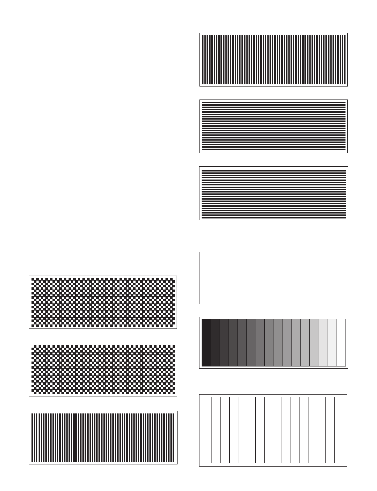
i. Black-and-white pattern in 1 dot interval
iv. Reversed pattern of pattern iii.
v. Horizontal stripe pattern in 1 dot interval
vi. Reversed pattern of pattern v.
vii. "H" pattern (80 digits × 35 lines) In the 35th line, only 78 digits
of "H" are displayed.
(The actual display range is 25 lines. Scroll for 10 lines to
check.)
HHHHHHHHHHHHHHHHHHHHHHHHHHHHHHHHHHHHHHHHHHHHHHHHHHHHHHHHHHHHHHHHHHHHHHHHHHH
HHHHHHHHHHHHHHHHHHHHHHHHHHHHHHHHHHHHHHHHHHHHHHHHHHHHHHHHHHHHHHHHHHHHHHHHHHH
HHHHHHHHHHHHHHHHHHHHHHHHHHHHHHHHHHHHHHHHHHHHHHHHHHHHHHHHHHHHHHHHHHHHHHHHHHH
HHHHHHHHHHHHHHHHHHHHHHHHHHHHHHHHHHHHHHHHHHHHHHHHHHHHHHHHHHHHHHHHHHHHHHHHHHH
HHHHHHHHHHHHHHHHHHHHHHHHHHHHHHHHHHHHHHHHHHHHHHHHHHHHHHHHHHHHHHHHHHHHHHHHHHH
HHHHHHHHHHHHHHHHHHHHHHHHHHHHHHHHHHHHHHHHHHHHHHHHHHHHHHHHHHHHHHHHHHHHHHHHHHH
HHHHHHHHHHHHHHHHHHHHHHHHHHHHHHHHHHHHHHHHHHHHHHHHHHHHHHHHHHHHHHHHHHHHHHHHHHH
HHHHHHHHHHHHHHHHHHHHHHHHHHHHHHHHHHHHHHHHHHHHHHHHHHHHHHHHHHHHHHHHHHHHHHHHHHH
HHHHHHHHHHHHHHHHHHHHHHHHHHHHHHHHHHHHHHHHHHHHHHHHHHHHHHHHHHHHHHHHHHHHHHHHHHH
HHHHHHHHHHHHHHHHHHHHHHHHHHHHHHHHHHHHHHHHHHHHHHHHHHHHHHHHHHHHHHHHHHHHHHHHHHH
HHHHHHHHHHHHHHHHHHHHHHHHHHHHHHHHHHHHHHHHHHHHHHHHHHHHHHHHHHHHHHHHHHHHHHHHHH
ii. Reversed pattern of pattern i.
iii. Vertical stripe pattern in 1 dot interval
4 – 10
viii. Gradation pattern from black to white in 16 gradations
ix. All white pattern
x. Color bar (16 colors)
Color bars of 16 colors are displayed.
Black
Blue
Green
Cyan
Red
Brown
White
Magenta
Gray
Light green
Light blue
Light cyan
Light red
Light magenta
Light yellow
Light white
Page 27
xi. Color pattern (256 colors)
Color pattern of 256 colors is displayed. The displayed colors
are the default pallet.
Arrange RAMDAC register No. 0 ∼ 255 from the upper left.
xii. Backlight OFF
The backlight is turned off without turning off the display.
xiii. Backlight ON
2 Terminating method
Press the space bar or Esc key to terminate and return to the
Serviceman’s diagnostics menu.
3-13. Magnetic Card Reader Diagnostics
This test program reads the magnetic card based on the ISO7811/1-5
standard and displays the data.
Pressing the Esc key returns to the service diagnostics menu.
1) Magnetic Card Reader Check
1 Checking content
The test program reads tracks 1 and 2 of the magnetic card (UKOG6718RCZZ) based on the ISO7811/1 ∼ 5 standard, and displays the
data in ASCII code. There ar e tw o kinds of data patterns to be read.
TRACK 1: IATA pattern
76 character 7bit/character (Max. 79 character)
TRACK 2: ABA data pattern
28 character, 5bit/character (Max. 40 character)
To read the card data, the following setting is performed.
• Mode set
46h is set to PSC2 channel 1 mode set register. (IATA, 6bit)
74h is set to PSC2 channel 2 mode set register. (ABA, 4bit)
• Start mark set
45h is set to PSC2 channel 1 start mark register.
0Bh is set to PSC2 channel 2 start mark register.
• Interrupt reset
Dummy data is written to PSC2 channel 2 start mark register.
• Interrupt mask cancel 01h is written to PSC2 MCR mask
register to cancel mask.
In addition, setting for the PSC2 extension interruption is per-
formed.
When the card is scanned, the obtained data is written to the
FIFO buffer from the start mark to LRC in sequence. Then, the
card data is read by interrupt process.
After reading data, the FIFO buffer is reset.
2 Display
The above display is made when the card (UKOG6718RCZZ) is
passed through the MCR. In case of an error, the error code is
displayed as follows:
Magnetic Card Reader Check
TRACK 1 : BUFFER EMPTY
TRACK 1 : MCR ERROR
TRACK 2 : BUFFER EMPTY
TRACK 2 : MCR ERROR
Displayed when TRACK1 EMPTY CODE is returned.
Displayed when TRACK1 ERROR CODE is returned.
Displayed when TRACK2 EMPTY CODE is returned.
Displayed when TRACK2 ERROR CODE is returned.
3 Terminating method
Press the Esc key to terminate the test and return to the
Serviceman’s diagnostics menu.
3-14. System Switch Diagnostics
The system switch information of the main PWB is displayed.
Pressing the Esc key returns to the serviceman diagnostics menu.
1) System Switch
Checking content
1
The system switch reads I/O address 7F0H every 10ms to display
the value of bit 0 ∼ 7. The relati onshi p betwee n the bit and SW is
as shown in the table below.
Bit76543210
7F0H SW8 SW7 SW1 SW2 SW3 SW4 SW5 SW6
2 Display
System Switch Diagnostics
SW1 SW2 SW3 SW4 SW5 SW6 SW7 SW8
XXXXXXXX
Each SW data is displayed at X. If bit data is "1," the display is
"OFF". If bit data is "0," the display is "ON".
3 Terminating method
Press the Esc key to terminate the test and return to the
Serviceman’s diagnstics menu.
3-15. Drawer Diagnostics
The drawer open and sensor test are executed.
The following menu is displayed. The highlighted cursor is moved by
the cursor keys (UP ↑ and DOWN ↓) of the AT keyboard. Move the
cursor to the desired item, and press the Enter key to execute the
selected diagnostics program. When the selected diagnostics program is completed, the display returns to the menu screen. Pressing
the Esc key returns to the service diagnostics menu.
Drawer Diagnostics
Drawer 1 Check
Drawer 2 Check
MCR (Magnetic Card Reader) Check
TRACK1:
SHARP TEST CARD 0123456789ABCDEFGHIJKLMNOPQRSTUVWXYZ0123456789 UKOG-6718RCZZ
TRACK2:
0123456789012345678901234567
1) Drawer 1 check
Checking content
1
The drawer 1 solenoid is turned on and the drawer open sensor
value is sensed at every 100ms and the state is displayed.
When Drawer 1 and Drawer 2 are connected, "CLOSE" is displayed only when both the drawers are closed.
4 – 11
Page 28
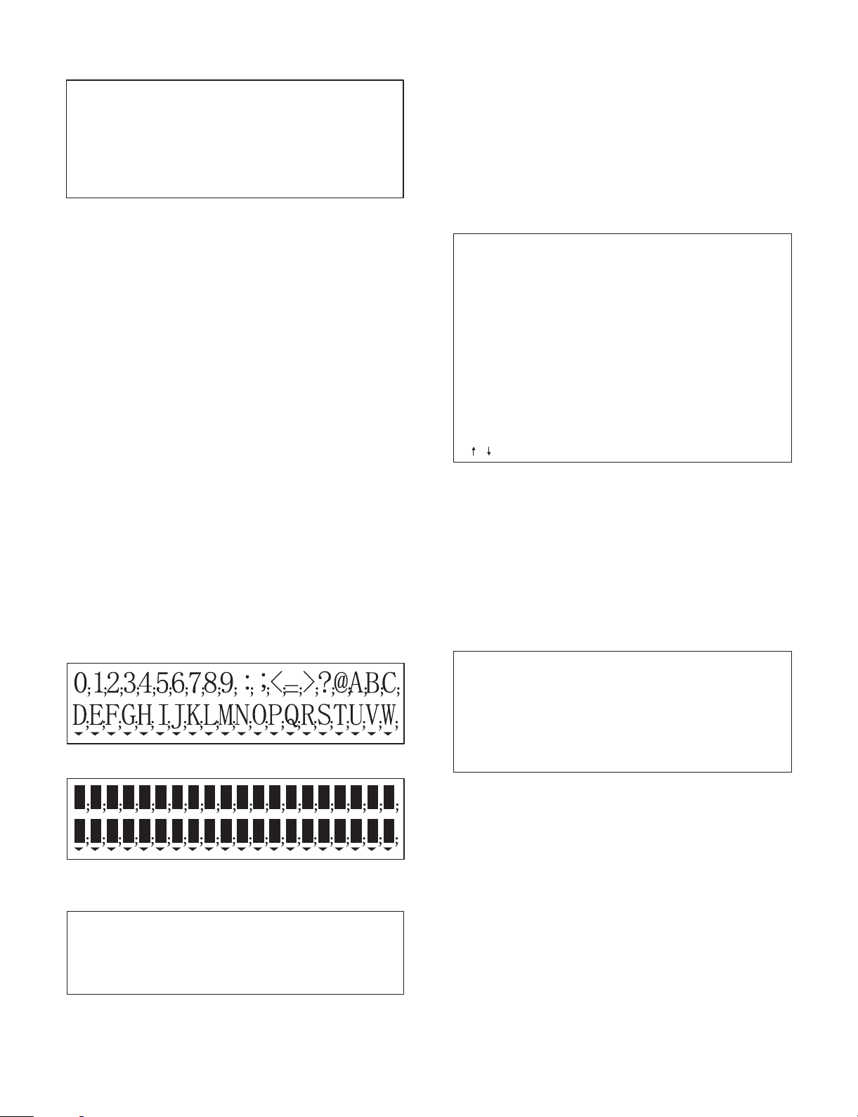
2 Display
Drawer 1 Check
Drawer Open Sensor : OPEN (or CLOSE)
3 Terminating method
Press the Esc key to terminate the test and return to the Drawer
diagnostics menu.
Pressing the ESC again will return to the serviceman’s diagnostics
menu.
2) Drawer 2 Check
1 Checking content
Drawer 2 solenoid is turned on and the drawer open sensor value
is sensed at every 100ms and the state is displayed.
When Drawer 1 and Drawer 2 are connected, "CLOSE" is displayed only when both the drawers are closed.
2 Display
Same as Drawer 1.
3 Terminating method
Same as Drawer 1.
3-16. Option Display Diagnostics
The option display includes a microprocessor inside that allows communication with the host by RS232 conforming interface.
PSC2 UART4 is used on the main body side.
Communication conditions are as follows:
• Data length: 8 bit
• Parity (Yes/No): No
• Baud rate: 9600bps
1 Checking content
The test patterns are displayed in the sequence shown below.
Pressing the space bar moves to the next pattern.
i. The following test patterns are displayed.
3-17. IDE I/F & Hard Disk Diagnostics
The hard disk is tested and the information stored in the hard disk is
displayed.
The following tests are executed.
• Read test: Seek (sequential, random) test, read only (target
cylinder, target sector), and dump test
• Write test: Write verify test (target cylinder, target sector), and
batch test.
• Other functions: Drive status display, controller check, error log -
ging area (error information) display, and error information display
Test screen (service repair only)
Hard Disk Drive Diagnostics
READ MODE TEST
Drive status display
Sequential seek test
Random seek test
Seek&Read test
Target Sector Read test
HD Dump test
Error LOGGING Information Display
Disk Controller Check test
WRITE MODE TEST
Seek&Write/Read-Verify test
Target Sector Write/Read-Verify test
HD Patch test
ERROR LOGGING AREA CLEAR
Error Table Display
, : Move ENTER : Selet ESC : Exit
On the above screen, select the desired test item with ↑ (UP) and ↓
(DOWN) keys and press the Enter key to execute the test. Pressing
the Esc key returns to the initial menu.
[READ MODE TEST]
1) Drive Status display
1 Checking content
The hard disk drive standard values (Memory capacity, Number of
cylinders. Number of heads, and Number of sectors) are displayed.
2 Display
Drive Status display
hard disk drive information
Drive Type : xxxxxx
Capacity : xxxxMB
Cylinder Number : xxx
Head number : xx
Sector number : xx
ii. The test pattern with all digits ON is displayed.
iii. All OFF
2 Display
Pole Display Check
3 Terminating method
Press the Esc key to turn off FD display and terminate the test and
return to the Option display diagnostics menu and the test is
terminated.
Press any key to exit.
Drive type: Hard disk drive name
Capacity: Hard disk memory capacity
Cylinder number: Max. cylinder number
Head number: Max. head number
Sector number: Max. sector number
3 Terminating method
Press any key to terminate the test and return to the menu screen
in the previous (1).
2) Sequential Seek Test
[Test conditions setting]
• Cylinder Range [0 ∼ inmost cylinder]
The cylinder range to be tested is set.
• Retry Count [0 ∼ 4]
Retry count in case of an error is set.
• Error Stop/Continue/1 Pass
Selection is made among Error Stop/Continue/1 Pass in case of an
error.
4 – 12
Page 29
• Test Start ? [Yes/No]
Selection is made to execute the test or not.
1 Checking content
In the cylinder range set above, the sequential seek is executed
for every 1 track. When the seek test in the set range is completed
(in the direction of 0 → inmost cylinder), it is counted as 1 pass. In
case of an error during the above test, a retry is repeated up to
the set number of retries. Every time an error occurs by executing
retry up to the retry number and error logging is performed. Logging is made for HD and DRAM.
When an "Error stop" is set in the test conditions setting, and an
error occurs during the above test, the error display is made and
the test is stopped. Press the space bar to resume the test.
When "Continue" is set, even if an error occurs, the error display
is made but the test is not stopped.
When "1 Pass" is set, a series of tests is made only once and the
test is stopped.
2 Display
Sequential Seek test execution screen
Sequential Seek test
@Cylinder range ?
[000 XXX] = 000-XXX
(XXX is displayed by checking the
inmost cylinder.)
@Retry count ?
[0 4] = 0
@[Errorstop continue 1pass]
@Test Start ? [Yes No]
Pass count = XXXXX
Test Point = CCC
ESC : Exit SPACE : Stop or Start
(Cylinder)
Select the desired items at the position of @. (@ is not displayed
on the screen.)
On the above screen, when the pass count is counted up (when
the point is counted up to the upper limit set in the cylinder range
setting, the pass count is counted up by 1.), and if the error
counter of all error items are not counted up (remaining as
00000), the test is OK.
When the space bar is pressed during the test, the test is inter-
rupted.
When the space bar is pressed during interruption of the test, the
test is started.
3 Terminating method
Press the Esc key during execution of the test or during interruption of the test to terminate the test and return to the above menu
screen.
3) Random Seek Test
[Test condition setting]
Same as the above sequential read.
However, execution of the test by 1 Pass means execution of random
seek through the set cylinder range.
1 Checking content
The random seek is executed for every one track in the cylinder
range set previously.
When the seek test is completed in the set range, it is counted as
1 pass.
In case of an error during the above test, a retry is repeated up to
the set number of retries. Every time an error occurs a retry is
performed up to the set number of retries and, error logging is
made. Logging is made for HD and DRAM.
When the "Error Stop" is set in the test condition setting, and an
error occurs during the above test, the error display is shown and
the test is interrupted. Press the space key to resume the test.
When the "Continue" is set, even if an error occurs, the error
display is made but the test is not stopped.
When "1 Pass" is set, a series of tests is made only once and the
test is stopped.
Error Kinds
Drive not ready XXXX
Bad controller XXXX
Compare error XXXX
Details of error are displayed.
2 Display
Same as the above sequential read, however the following contents are different.
The test Point is changed at random in the range of 000 ∼ XXX
(cylinder range set value).
Each point is tested once, and the pass count is added by one
with XXX times.
3 Terminating method
Press the Esc key during execution of the test or during interruption of the test to terminate the test and return to the above menu
screen.
4) Seek & Read Test
[Test condition setting]
Same as the above sequential read. The following setting is additionally required.
• Sector count [0 ∼ final sector]
The sector range to be tested is set.
1 Checking content
The sequential read for every one track is executed in the cylinder
range and the sector range set above. (in the direction of 0 →
inmost cylinder)
When the read test is completed in the set range, it is counted as
1 pass.
Before seeking, however, seek is made the previous cylinder and
the following cylinder.
(Head movement)
When track N is read, the head moves as follows:
0 cylinder
S-1
The previous
cylinder
1
S
Cylinder to be tested
N-1 N-1
N
2
4
Next
At 2 and 4, read is executed.
In case of an error during the above test, a retry is repeated up to
the set number of retries. Every time an error occurs a retry is
performed up to the set number of retries and, error logging is
made. Logging is made for HD and DRAM.
When the "Error Stop" is set in the test condition setting, and an
error occurs during the above test, the error display is shown and
the test is interrupted. Press the space key to resume the test.
When the "Continue" is set, even if an error occurs, the error
display is made but the test is not stopped.
When "1 Pass" is set, a series of tests is made only once and the
test is stopped.
2 Display
Seek & Read test
@Cylinder range ?
[000 XXX] = 000-XXX
(XXX is displayed by checking the
inmost cylinder.)
@Sector count ?
[0 XX] = XX
(XXX is displayed by checking the
inmost cylinder.)
@Retry count ?
[0 4] = 0
@[Errorstop continue 1pass]
@Test Start ? [Yes No]
Pass count = XXXXX
Test Point = CCC : HH : SS
ESC : Exit SPACE : Stop or Start
Select the desired items at the position of @. (@ is not displayed
on the screen.)
(Cylinder: head; sector)
S+1
The next
cylinder
3
Error Kinds
Drive not ready XXXX
Bad controller XXXX
Compare error XXXX
Details of error are displayed.
Inmost
cylinder
4 – 13
Page 30
(On the above screen, the thick figures are selected, and the thick
figure values are selected.)
On the above screen, when the pass count is counted up (when
point is counted up to the upper limit set in the cylinder range
setting, the pass count is counted up by 1.), and if the error
counter of all error items are not counted up (remaining as
00000), the test is OK.
3 Terminating method
The methods to interrupt, resume, and terminate the test are the
same as (2) Sequential read.
5) Target Sector Read Test
[Test conditions setting]
• Cylinder range [0 ∼ inmost cylinder]
The cylinder range to be tested is set.
• Head count [0 ∼ final head]
The head umber to be tested is set.
• Sector count [0 ∼ final sector]
The sector number to be tested is set.
• Retry count [0 ∼ 4]
Retry number incase of an error is set.
• Error stop/Continue/1 Pass
Selection is made among Error Stop/Continue/1 Pass in case
of an error.
• Test start ? [Yes/No]
Selection is made between Yes/No of test start.
1 Checking content
A read is made for the cylinder range, the head number, and the
sector number areas set in the above.
When the read test is completed in the set range, it is counted as
1 pass.
In case of an error during the above test, a retry is repeated up to
the set number of retries. Every time when an error occurs a retry
is performed up to the set number of retries and, error logging is
made. Logging is made for HD and DRAM.
When the "Error Stop" is set in the test condition setting, and an
error occurs during the above test, the error display is shown and
the test is interrupted. Press the space key to resume the test.
When the "Continue" is set, even if an error occurs, the error
display is made but the test is not stopped.
When "1 Pass" is set, a series of tests is made only once and the
test is stopped.
2 Display
Target Sector Read test
@Cylinder range ?
[000 XXX] = 000-XXX
(XXX is displayed by checking the
inmost cylinder.)
@Head count ?
[0 XX] = 0
XX is displayed by checking the
(
final head.)
@Sector count ?
[0 XX] = XX
XX 8s displayed by checking the
(
max. sector.)
@Retry count ?
[0 4] = 0
@[Errorstop continue 1pass]
@Test Start ? [Yes No]
Pass count = XXXXX
Test Point = CCC : HH : SS
ESC : Exit SPACE : Stop or Start
(Cylinder: head; sector)
Select the desired items at the position of @. (@ is not displayed
on the screen.)
(On the above screen, the thick figures are selected, and the thick
figure values are selected.)
On the above screen, when the pass count is counted up (when
point is counted up to the upper limit set in the cylinder range
setting, the pass count is counted up by 1.), and if the error
counter of all error items are not counted up (remaining as
00000), the test is OK.
Error Kinds
Drive not ready XXXX
Bad controller XXXX
Compare error XXXX
Details of error are displayed.
3 Terminating method
The methods to interrupt, resume, and terminate the test are
same as (2) Sequential read.
6) HD Dump Test
[Test conditions setting]
• Cylinder No. [0 ∼ inmost cylinder]
A certain cylinder No. to be displayed is set.
• Head No. [0 ∼ final head]
A certain head No. to be displayed is set.
• Sector No. [1 ∼ final sector]
A certain sector No. to be displayed is set.
1 Checking content
The sector set in the above is displayed on the screen in the unit
of 256byte.
Hex data and ASCII characters are displayed.
By key operation, the following 256 byte data or previous 256byte
data can be displayed.
2 Display
HD Dump test
@Physical address ? [CCC. HH. SS] = 000. 00. 01
The first hslf sector
000 : HHHH......HHHH-HHHH......HHHH : AAA......AA
(100)
010 : HHHH......HHHH-HHHH......HHHH : AAA......AA
(110) :
020 : HHHH......HHHH-HHHH......HHHH : AAA......AA
(120) :
:
0F0 : HHHH......HHHH-HHHH......HHHH : AAA......AA
(1F0) :
PGDN : forward PGUP : back SPACE : Start ESC : Exit
The physical address is set at the position of @. (On the above
screen, the thick value is set.)
On the above screen, the first-half 256 byte at 000 cylinder, 00
head, and 01 sector is displayed.
Press the page down key to display the second-half 256 byte.
(When the page down key is pressed on the above screen, the
second-half 256byte at 000 cylinder, 00 head, and 01 sector is
displayed.)
Press the page up key to display the first-half 256byte.
3 Terminating method
Press the Esc key to return to the menu screen of previous (1).
7) Error Information Display
1 Checking content
Error information stored in the inmost area of the HDD is displayed.
When the hard disk test is executed, error information stored in
the error information storing area is displayed.
The inmost cylinder, 0 head, and 1 sector ∼ 6 sector are read to
be displayed.
2 Display
Error Logging information Display
Error
No.
001
002
003
004
005
006
007
YY/MM/DD
99 / 03 / 01
HH : MM : SS
10 : 30 : 00
ESC : Exit ENTER : Next
Every time the Enter key is pressed, the next page error information is displayed.
:
Cyl
No.
100
Hed
No.
03
Sec
No.
01
Error
Content
XXXXXXX
4 – 14
Page 31

[Descriptions on the above screen]
Error No. ———— Error information register No. (001 ∼)
(This is not an error code.)
YY/MM/DD ——— Year/Month/Day
HH:MM:SS ——— Hour/Minute/Second
Cylinder ———— Cylinder No.
Head No. ———— Head No.
Sec No. ————— Sector No.
Error Content —— Error code is converted into error content
and displayed.
3 Terminating method
Press the Esc key to return to the menu screen.
8) Controller check test
1 Checking content
The diagnostic command included in the F-ROM is executed to
perform hard disk controller check.
2 Display
Disk Dontroller Check test
@[Errorstop Continue 1pass]
@Test Start ? [Yes No]
Pass count = XXXXX
Controller ..... Checking
(Test for 1 pass)
The write is made in the direction of 0 → inmost cylinder.
The read/verify check is made in the direction of 0 → inmost
cylinder.
The write is made in the direction of inmost cylinder → 0.
The read/verify check is made in the direction of inmost cylinder
→ 0.
When writing data, write different data from the original stored
data.
Before writing or reading, the head is moved to the previous or the
following cylinder.
(Head movement)
When track N is read, the head moves as follows. (The head arm
is deflected back and forth.)
In the direction of 0 → inmost cylinder
0 cylinder
The previous
cylinder
1
Cylinder to be tested
N-1 N+1N
2
4
Next
The next
cylinder
3
Inmost
cylinder
ESC : Exit SPACE : Stop or Start
If the section blinks and the pass count is counted up, the
test is OK.
When the space bar is pressed during the test, the test is interrupted.
When the space key is pressed during interruption of the test, the
test is resumed.
3 Terminating method
When the Esc key is pressed during the test or test interruption,
the test is terminated and the display returns to the menu screen.
[Write mode test]
(Note) When the following test is executed, the HDD data is
destroyed.
The display shown before executing write mode test
When executed, Data on hard disk will be destroyed.
Password ? [*****]
ESC : Exit
Before executing the write mode test, "When executed, Data on
hard disk will be destroyed." is displayed.
Password entry is urged. Only when the correct password is
entered, does the display go to the next one.
The correct password is "sharp" or "SHARP" in 5 digits. When
typing the correct password, the content is not displayed but "*" is
displayed.
9) Seek & Write/Read-Verify Test
[Test conditions setting]
Similar to the above 4). Cylinder range setting is 000 ↔ inmost
cylinder 2.
1 Checking content
For all the cylinder range and the sector range set in the above,
the worst pattern data is written sequentially for every one track.
Then, the read/verify check is made for every one track.
The number of the read/verify check is one.
Note message
Writing is made at 2.
Reading is made at 2 and 4.
In the direction of 0 ← inmost cylinder
0 cylinder
S-1
The previous
cylinder
3
S
Cylinder to be tested
N-1 N-1
N
2
4
Next
S+1
The next
cylinder
1
Writing is made at 2.
Reading is made at 2. and 4.
(Worst pattern data)
There are two kinds of worst data: B6DBH and 6DB6.
In case of an error during the above test, a retry is repeated up to
the set number of retries. Every time an error occurs a retry is
performed up to the set number of retries and, error logging is
made. Logging is made for HD and DRAM.
When the "Error Stop" is set in the test condition setting, if an error
occurs during the above test, the error display is shown and the
test is interrupted. Press the space key to resume the test.
When the "Continue" is set, even if an error occurs, the error
display is made but the test is not stopped.
When "1 Pass" is set, a series of tests is made only once.
2 Display
Same as the previous (4). The following two points are different.
* Cylinder range ?
[000 ↔ XXX] (XXX is inmost cylinder 2.)
* Test mode: is displayed.
When data writing, WRITE is displayed in . When data
reading, READ is displayed.
3 Terminating method
Same as (4).
Inmost
cylinder
4 – 15
Page 32

10) Target Sector Write/Read-verify Test
[Test conditions setting]
Similar to the previous 5). Cylinder range setting is 000 ↔ (Final
cylinder 2).
1 Checking content
For the cylinder range, the head number, and the sector number
area set in the above, write/read/verify is made.
When the write/read test is completed in the set range, it is
counted as 1 pass.
In case of an error during the above test, a retry is repeated up to
the set number of retries. Every time an error occurs a retry is
performed up to the set number of retries and, error logging is
made. Logging is made for HD and DRAM.
When the "Error Stop" is set in the test condition setting, if an error
occurs during the above test, the error display is shown and the
test is interrupted. Press the space key to resume the test.
When the "Continue" is set, even if an error occurs, the error
display is made but the test is not stopped.
When "1 Pass" is set, a series of tests is made only once.
2 Display
Same as the previous (6). The following two points are different.
* Cylinder range ?
[000 ↔ XXX] (XXX is inmost cylinder 2.)
* Test mode: is displayed.
When data writing, WRITE is displayed in . When data
reading, READ is displayed.
3 Terminating method
Same as 5).
11) HD Patch Test (Utility)
[Test conditions setting]
Similar to the previous 6). The cylinder range setting is 000 ↔ (Final
cylinder 2).
1 Checking content
The sector set in the above is displayed on the screen in the unit
of 256byte.
Hex data and ASCII characters are displayed.
By key operation, the following 256 byte data or previous 256byte
data can be displayed.
After changing data on the screen, data is written to the selected
set position.
2 Display
Similar to the previous 6). Data in the HDD can be patched.
Patching is made as follows:
To patch data in the HD, change data on the screen.
(Move the cursor with ↑, ↓, ←, →, keys and enter data with 0 ∼ F
key.
Then select "Yes" in "Up data ? [Yes/No]" and press Enter key.
(Move with ← key.)
With the above procedure, patch is made.
3 Terminating method
Same as 6).
12) Error Logging Area Clear
Checking content
1
The last cylinder area in the HD is cleared with 00H.
(Error logging area: last cylinder, all sectors of 0 head)
The areas to be cleared with 00H is the last cylinder and all the
sectors of 0 head.
2 Display
Error Logging Area Clear
@Test Start ? [Yes No]
, : Move ESC : Exit ENTER : Select
ESC : Exit SPACE : Retry
At first No is highlighted.
Guidance before execution of the test
Guidance after execution of the test
Select "Yes" at position @ (move with ← key) and press the Enter
key to execute the test.
When the test is executed once, the mode enters the key waiting
mode. After executing the test, press the space key to execute
again.
3 Terminating method
Press the Esc key to return to the menu screen.
13) Error table display
When an error occurs during the above test, error information is
stored in the DRAM and the content is displayed.
If there is no error, OK or NO ERROR is displayed.
14) Supplemental items
Error information is stored up to 44 items in the sequence of occurrence from when the function is selected. If the item number exceeds
44, the error information is not stored any more.
15) Error content
The following error content is error information directly obtained from
the HDD controller.
[Error code and meaning]
Error code Error message
0
1
OK (This message is displayed when the test is
normally completed.)
Drive not ready (HDD is not ready. STATUS REG bit
6 : 0)
Bad controller (HDD controller abnormality, diag
2
status error STATUS REG bits : 1 or DIAG STATUS
>= 2)
3
4
5
6
7
8
9
10
11
Track 000 Error (TRACK 000 cannot be found with
RESTORE command. ERROR REG bit 1 : 1)
Seek Error (A seek error occurs. After STATUS
COMMAND is executed, STATUS REG bit 4 : 0)
ID not Found (ID field is not detected. ERROR REG
bit 4 : 0)
Data Address Mark not Found (Data Address Mark
is not found. ERROR REG bit 0 : 1)
Bad Block Detect (BAD block mark is stored in the
ID field of request sector. ERROR REG bit 7 : 1)
Uncorrectable error (An uncorrectable read error
occurs. ERROR REG bit 6 : 1)
Others error (The other error STATUS REG bit 0 : 1,
and ERROR REG : 0)
Time out error (Time out occurs when making
access to HDD.)
Compare error (The written data and the read data
are not the same.)
16) Error information storing area
1 Error information storing area for diagnostics
1 sector ∼ 6 sector of 0 head of the last cylinder is used.
Used in the following format from the head of each sector.
(Error information format for every sector)
1 + 46 × 11 = 507byte is used in one sector.
4 – 16
Page 33

Last cylinder
Head of 0 head, 1 sector
2nd sector - 6th sector are the same.
4 Terminating testing
When the screen displays the following message, remove the FD
and press any key.
Counter
BIN
Error
code
BIN BIN BIN BIN BIN BCD BCD BCD BCD BCD BCD
[1byte 0~46]
Cylinder
(L) (H)
Head Sector
Year
Month
Day
Hour Minute
3-18. FDD Diagnostics
This is a test program that checks floppy disk drives.
(Do not use this program after performing a D-RAM test.)
1) FDD Check
1 Description
A test file is opened on a floppy disk and data (256 bytes) of 00h FFh is written four times on the disk before read and verification
are performed.
2 Display
After making sure the screen looks like this, insert a formatted FD
(W/R-TEST disk) into the drive and press any key.
Please insert W/R-TEST disk to drive A:
Data in the disk A: will be destroyed.
Note: The hatched drive name is [A:] or [B:].
W/R-TEST disk: Formatted FD (Turn off write-protection)
The screen looks like this during testing.
FDD Write/Read & Compare Check
3 Error
When an error occurs, the following message appears on screen.
Warning
Second
Please out W/R-TEST disk from drive A:
Note: The hatched area is the drive name [A:] or [B:].
3-19. Fan & LCD ON/OFF Diagnostics
1) Fan & LCD ON/OFF Check
1 Checking content
The CPU, the fan, the exhaust fan and the LCD are turned
ON/OFF.
When this menu is selected, the following display is shown.
FAN&LCD ON/OFF Diagnostics
HIT ANY KEY
When any key is pressed, "1" is written to bit 4 of PSC2 general
use I/O port HIOP. At that time, the CPU fan and the exhaust fan
are stopped and the LCD and the backlight are turned off.
When any key is pressed under this state, or if there is no key
input for 10 sec, the display automatically returns to the main
menu and the test is terminated.
When the system exits this diagnostic job, "0" is written to HIOP
bit 4.
3-20. Power Hold Diagnastics
1) Power Hold Check
1 Checking content
Two types of states such as power hold and power switch are
displayed.
Power Hold Diagnostics
Power Hold : ON (or OFF)
Power Switch : ON (or OFF)
When pressing the space key, bit 5 of PSC2’s general I/O port
HIOP is inverted, and power hold is switched between ON and
OFF.
In addition, bit 1 of PSC2’s general port HIOP is read at every
200ms. Power Switch: OFF is displayed when this bit is "0", and
Power Switch: ON is displayed when this bit is "1".
**********
********** FDD ERROR !!! **********
Drive not ready
Note: An error message appears at the hatched area
Error message Description
Drive not ready No FD in drive
Verify error Write data is different from Read data
Write protect error Disk is write-protected.
General failure FD is not formatted or others
No space left on device No disk space available
Other than those message, some MS-DOS error message may be
displayed.
4 – 17
Page 34

CHAPTER 5. CIRCUIT DESCRIPTION
1.
1-1. CPU
Pentium Processor: A80502CSLM66133SY028
• External Bus Interface: 66MHz
• L1 cache: 8K Code & 8K Data (Writeback) cache
• 64-Bit Data Bus
1-2. Chipset
FireStar Plus: 82C700U3.2
• PCI Bus:
• DRAM controller
(FPM, EDO or SDRAM): FPM or EDO supported
• ISA Bus: AT Clock = 8.33MHz
• Bus Mastering IDE: Primary IDE supported, Not Secondary
• Thermal Management: Not used
• Unified Memory Management (UMA):
• DMA controller: 8237A × 2
• Interval Timer: 8254
• Interrupt controller: 8259 × 2
1-3. PS/2 Keyboard Controller
KBC: M38802M270
• Full keyboard control
• Mouse control: Not used
• Matrix Key control: Not used
1-4. Graphic Controller
VGAC: MN89305
• XGA compatible
• LCD (640 × 480 × 256/64k color; 800 × 600 × 256/64k color; 024 ×
768 × 256 color) control
• Host intrface: PCI/ISA/I386/I486/VL interface (Used
for PCI interfce)
• DRAM interface: 4M DRAM (16-bit) × 1or2, 16M DRAM
(16-bit) × 1or2
• Vcc=3.3V only
1-5. Super I/O Controller
M5113A2
• FDC: Disable
• Serial Port: 16C550 compatible with Infrared × 2
• Parallel Port: used for LPT1
1-6. System Controller 2
PSC2: LZ9AM22
• BIOS ROM Bank Control: Fixed 2banks
• Mask ROM Bank Control: Fixed 256banks
• Flash ROM Bank Control: Max. 384banks
• PS-RAM Bank Control: Max. 192banks
• UART × 5: COM 5ch
• Clocked Serial I/O × 2: CKDC VII I/F (Not used)
• Mode Switch Sense: 16bits (Not used)
• Clerk Switch Sense: 16bits (Not used)
• MCR I/F: 2track
• Drawer I/F: 2drawers
1-7. Memory
• L2 cache: None
• System Memory: DRAM Standard = 1M × 16b EDO
Asym 60ns Vcc = 3.3V × 4chip (8MB)
Option = 144pin S.O.DIMM socket
× 1 (8MB/16MB/32MB)
• BIOS ROM: 512K × 8b (512KB) Flash ROM
Vcc = 5.0V
• DOS ROM: 1M × 16b (2MB) Mask ROM
Vcc = 5.0V
• Flash ROM Disk: Standard = 1M × 16b (2MB)
Vcc = 5.0V
Option = 2M × 16b (4MB)
• PS-RAM Disk: Standard = 512K × 8b × 2chip (1MB)
Vcc = 3.3V
Option = 512K × 8b × 4chip (2MB)
• Video RAM: 256K × 16b × 2chip (1MB)
Vcc = 3.3V
1-8. Analog Touch Panel
• Controller: N010-0559-V021
• RS-232C I/F (2400/4800/9600bps):
used for 9600bps
• Resolution: 1024 × 1024
1-9. LCD
• Color LCD: 10.4" DSTN 640 × 480 × 256color
1-10. System Switch
• DIP Switch: 8circuits
• Jumper Switch: Not used
• 0Ω Register: Not used
1-11. Serial Ports
• Serial 1 (Used for COM1): Ci/+5V switchable – DSUB9 with FIFO
(by Super I/O)
• Serial 2 (Used for COM2): Ci/+5V switchable – DSUB9 with FIFO
(by Super I/O)
• Serial 3
(Used for COM3/5):
• Serial 4
(Used for COM4/6):
SG/+5V Pattern-cut & Jumper – RJ45
without FIFO (by PSC2)
– RJ45 without FIFO (by PSC2)
• Serial 5: Used for Built-in printer – TTL level in-
terface
• Serial 6: Used for Customer VFD control –
RJ45(for UP-P20DP) or 7pin-CN(for
UP-I20DP)
• Serial 7: Used for Touch panel control – TTL
level interface
1-12. Power Supply Unit
• Input = AC100 - 120V, 50/60Hz
1-13. Vacuum Fluorescent Display Unit:
202MD11AB (used Pole display unit:
UP-P20DP/i20DP)
• VFD = 20 Digits × 2 Lines, 5 × 7dots with; (Period & Comma) + 20
w
• Microcontroller with Character Generator
• RS-232C I/F (RXD/DSR/DTR,4800/9600/19200/38400bps):
used for 9600bps
• Power: +5VDC/1A
• Auto indicator blinking: When power is turn on, automatically
blink the indicator of 1st digit.
5 – 1
Page 35

2. Block Diagram
Power
Supply
VGA PCB
Video RAM
1MB
CCFT
Inveter
LCD
Analog
Touch Panel
+5V
+12V
-12V
GND
25.175MHz
VGAC
MN89305
Buffer
TCP PCB
TPC
N010-0559-V021
8MHz
Main PCB
Pentium
14.318MHz
CG
MK1492-04R
32.768kHz
Serial7
HA
HD
ctrl
AD
ctrl
AD
PCI Bus
PS/2 KBC
M38802
M270
7.37MHz
PSC2
FireStar Plus
82C700U3.2
SA
Dctrl
SD
Dctrl
SA
SD
SD
MA
MD
RAS/CAS
32.768kHz
RTC
bq3285ESS
24MHz
Super I/O
M5113A2
Buzzer
EIDE
EDO DRAM
144pin
S.O.DIMM
3.3V DC-DC
Convetor
Serial1
Serial2
Parallel1
2.5" HDD
PS/2
Keyboard
3.5" FDD
UP-H14FD
COM1
COM2
LPT1
COM3/5
COM4/6
UP-T80BP
UP-P20DP
UP-I20DP
Drawer
MCR
System SW
Serial3
Serial4
Serial5
Serial6
Driver
ISA Bus
BIOS
ROM
512kB
DOS
ROM
2MB
Std.
PS-RAM Disk
1MB
Opt.
PS-RAM Disk
2MB
ISA
slot
Std.
F-ROM Disk
2MB
Opt.
F-ROM Disk
4MB
ER-A8RS
Ethernet
5 – 2
Page 36

3. Memory Map
Main Memory(System)
0000000
0800000
1000000
1800000
EDO DRAM
Standard
8MB
FPM/EDO DRAM
Option
8Byte SOD
8MB
FPM/EDO DRAM
Option
8Byte SOD
16MB
FPM/EDO DRAM
Option
8Byte SOD
32MB
A0000
C0000
C8000
VGA RAM
128KB
VGA BIOS
32KB
UMB
124KB
NOTE:
When the system installer is started, the System
BIOS ROM uses addresses from C0000h to
CAFFFh. Use caution not to let addresses contend
with each other when using an ISA option boards
equipped with BIOS ROM.
27FFFFF
E8000
EC000
F0000
FFFFF
ROM Disk 16KB
RAM Disk 16KB
System BIOS
64KB
M-ROM(Bank0-255)
F-ROM(Bank512-895)
PS-RAM(Bank0-191)
5 – 3
Page 37

4. I/O Address Map
4-1. PC specification
Address Legacy ISA I/O
00-0F DMA ch0-3 control
10- 1F (System)
20- 21 Master 8259 Interrupt control
22- 24 Chipset Configuration
40- 43 Timer control
48- 4B (Timer control)
50-52 (System)
60- 6F Keyboard/Mouse control
70- 7F RTC/CMOS RAM Index/Data
80- 8F DMA Page Register
90- 9F System Port A Register (PS/2 port)
A0-A1 Slave 8259 Interrupt control
C0-DE DMA ch4-7 control
F0- F1 (Coprocessor busy clear/reset)
102 65550(VGAC) Global Enable Register
110-16F
170-177 Secondary IDE control
180-19F POS I/O
1A0-1EF
1F0-1F7 Primary IDE control
200-26F
278-27F [Parallel Port 2 (LPT2) control]
280-2DF
2E8-2EF COM4 control
2F0-2F7
2F8-2FF COM2 control
300-36F
378-37F Parallel Port 1 (LPT1) control
380-38F
398 Super I/O Configuration Port
3A0-3AF
3BC-3BF [Parallel Port 3 (LPT3) control]
3C0-3DF EGA/VGA control
3E0-3E4 PCIC PCMCIA controllers
3E5 [BIOS ROM Write Control]
3E8-3EF COM3 control
3F0-3F7 FD/HD control
3F8-3FF COM1 control
400-40A
40B EISA DMA Extended Mode control
410-4EF
4D6 EISA DMA Extended Mode control
4D7-57F
580-59F POS I/O
5A0-7EF
7F0-7F1 PSC Special System Register
7F2-7FF
800-97F
980-99F POS I/O
9A0-A78
A79 [(PnP ISA Auto Configuration Port)]
A7A-BFF
C00-CF7
CF8-CFF PCI Configuration
D00-D7F
D80-D9F Reserved [POS I/O]
DA0-FFF
4-2. POS specification
Address POS I/O
180-189 Extended Interrupt control F
18A Drawer control F
18B-18F Timer Counter control F
190-191 CSIO1 (CKDC) control Reserved
192-193 CSIO2 (CKDC) control Reserved
194 BIOS Bank control F
195 ROM & RAM Disk Base Address F
196-197 Interrupt Status Read F
198-199 Mask/Flash ROM Bank control F
19A-19B PS-RAM Bank control F
19C-19D Mode Switch Reserved
19E-19F Clerk Switch Reserved
580-585 MCR control F
588 General Purpose I/O F
590-597 COM5 (Serial3) control F
598-59F COM6 (Serial4) control F
980-987 Serial5 (Built-in Printer) F
988-98F Serial6 (CU.VFD) control F
990-997 Serial7 (Touch Panel) control F
D80-D8F [Option]
D90-D9F [Option]
5. DMA Channel Mapping
DMA Channel Legacy ISA DMA function
0 ISA Expansion
1—
2 Floppy Disk Controller
3 ECP parallel port on LPT1
4 [Cascade]
5—
6—
7—
UP-5300
U/A
5 – 4
Page 38

6. IRQ
6-1. IRQ Mapping list
Controller1
8259
IRQ0 System timer Timer Timer Timer
IRQ1 Keyboard KBC KBC KBC
IRQ2 PIC cascade (Cascade) (Cascade) ✕
IRQ3
IRQ4
IRQ5 (LPT2) ISA ISA LPT2†
IRQ6 FDC FDC FDC FDC
IRQ7 LPT1 LPT1 LPT1 LPT1
† = ER-A8RS(Serial 2ch & Parallel 1ch) may be used.
[ ] = This function is used with 0ohm Resistor, etc.
Controller2
8259
IRQ8 RTC/CMOS RTC/CMOS RTC/COMS RTC/CMOS
IRQ9 — IRQx IRQx IRQx
IRQ10 (COM4) ISA/Serial4 Serial4/3/7/ISA COM4†
IRQ11 (COM3) ISA/Serial3 Serial3/4/7/ISA COM3†
IRQ12 Mouse ISA/[KBC] ISA/[KBC] SRN/Ethernet
IRQ13 Coprocessor ✕✕✕
IRQ14 Primary IDE HDC HDC HDC
IRQ15 Secondary IDE Serial7 Serial7/3/4/IRQx Touch Panel
Fixed ISA
Power On
Default
COM2 Serial2 Serial2 COM2
COM4 ✕/Serial4 ✕/Serial4 ✕
COM1 Serial1 Serial1 COM1
COM3 ✕/Serial3 ✕/Serial3 ✕
Extended Interrupt On-Board POS Device
Default
IRQx0 MCR (UP-E12MR2)
IRQx1 Serial5 [Built-in Printer] UP-T80BP
IRQx2 Serial6 [VFD] UP-P20DP/I20DP
IRQx3 POS Key (Not used)
IRQx4 CSIO1 I/F (Not used)
IRQx5 CSIO2 I/F (Not used)
IRQx6 FROM Busy
IRQx7 POFF
IRQx8 SINT0
IRQx9 Reserved [Mode Switch] (Not used)
IRQx10 TC0OVF
IRQx11 TC0CMP
IRQx12 TC1CMP
IRQx13 Serial4 (COM6)
IRQx14 Serial3 (COM5)
IRQx15 Clerk Switch (Not used)
Available Device
UP-5x00
Recommended
5 – 5
Page 39

6-2. IRQ Block Chart 6-3 IRQ Switch
Pentium
FireStar
IRQ9
IRQ15
IRQ3
IRQ4
IRQ10
IRQ11
IRQ5
IRQ6
IRQ7
IRQ12
IRQ1
IRQ8#
IRQ14
PIRQ9
PIRQ15
PIRQ3
PIRQ4
PIRQ10
PIRQ11
PSC2
+5V
+5V
0
+5V
IRQ9
IRQ15
Mask n
IRQn
IRQ3
IRQ4
IRQ10
IRQ11
10K
IRQ5
1K
10K
10K
KBC
KIRQ12
IRQ1
IDE CON
DIRQ
2.7K
+5V
+5V
10K
10K
10K
ISA Slot
IRQ9
IRQ15
IRQ3
IRQ4
IRQ10
IRQ11
IRQ5
IRQ6
IRQ7
IRQ12
IRQ14
+5V
10K
0
+5V
0
2.7K
+5V
0
2.7K
+5V
1
3
1K
Super I/O
SICF(IRQ9)
IRQ10
IRQ11
IRQ3
IRQ4
IRQ5
10K
IRQ6
IRQ7
+5V
10K
RTC
IRQ8#
=Not used
Riser board (parts side)
IRQ11 IRQ10
M
(3)
S1 = IRQ10: S(1) = ON (Connect IRQ10 to the ISA Slot.)
S2 = IRQ11: S(1) = ON (Connect IRQ11 to the ISA Slot.)
S
(1)M(3)
S2
M(3) = OFF (Connect IRQ10 to GND, not to the ISA
M(3) = OFF (Connect IRQ11 to GND, not to the
S
(1)
S1
Slot.)
ISASlot.)
7. CPU
7-1. Introduction
Intel’s Pentium Processor (A80502CSLM66133SY028) is used.
Pentium Processor Bus Frequency Selection
Core Frequency
(max)
100MHz 66MHz 2/3 1 1 UP-5300 Setting
Setting 1 = 10kohm Pull up (Vcc3)
0 = 0ohm Grounding
MicroClock MK1492-04R Power-up Input Setting
Pin # Name Internal Resistor Setting Function
5 OE Mid-level Default All Clock Outputs Enabled
15 CPUS# Pull up Default
16 PCISTP# Pull up Default HOST = 66.66MHz
24 FS Pull up Default
27 CSSS Pull up Default Power Down Mode = All Clocks On
19 DS Pull up Default HOST7,8 Tristated
21 SEL0 Pull up Default 48M/14.3M = 48.0MHz
22 LE Pull up Pull down EMI Control ON
25 SEL1 Mid-level Default F1 = 14.318MHz
28 PEN Mid-level Default Pin25 = PCI, Pin24=PCIF
The external pull down resistor is 10kohm.
External Bus
Frequency (max)
Bus/Core
Ratio
BF1
(Y33)
5 – 6
BF0
(Y35)
Selection
Page 40

MicroClock MK1492-04R Clock Output
Pin
Name Condition
#
5 14.3 14.318MHz for FireStar
8 EHOST1 Early CPU Clock for FireStar
10 HOST2 CPU Clock for Pentium
12 HOST3 Not used (Host Output Clock)
13 HOST4 Not used (Host Output Clock)
18 HOST5,7 Not used (Host Output Clock)
19 HOST6,8 Not used (Host Output Clock)
21 48M/14.3M Not used (48.0MHz Clock)
22 PCIF Not used (PCI Clock)
24 PCI Not used (PCI Clock)
25 PCI Not used (PCI Clock)
27 PCI PCI Clock for FireStar
28 F1 Not used (14.318MHz Clock)
7-2. Pin assignments
4
6
8
10
12
2
1
3
5
7
9
AM
AN
AK
AH
AG
AE
AD
AC
AB
AA
INC
NC
AL
INC
AP#
AJ
BREQ
VSS
VCC2
AF
VSS
VCC2
VSS
VCC2
VSS
VCC2
Z
VSS
Y
VCC2
X
VSS
W
VCC2
V
VSS
U
VCC2
T
VSS
S
VCC2
R
VSS
Q
VCC2
P
VSS
N
VCC2
M
VSS
L
VCC2
K
VSS
J
VCC2
H
VSS
G
VCC2
F
DP6
E
D54
D
D50
C
INC
B
INC
A
INC
FLUSH#
BUSCHK#
D46
D44
DP4
VCC2
VSS
VSS
BE0#
A20M#
BE1#
D42
D40
D39 D37 D35 D33
D38
VSS
VSS
INC
EADS#
WR#
PWT
HITM#
D/C#
HIT#
HLDA
ADS#
LOCK#
SMIACT#
PCD A27
PCHK#
NCNCAPCHK#
NC
PRDY
HOLD
WB/ WT#
NC
BOFF#
NA#
NC
BRDY#
KEN#
EWBE#
AHOLD
INV
CACHE#
MI/O#
BP3
BP2
PM1BP1
FERR#
PM0BP0
IERR#
DP7
D63
D62
D60
D61
D59
D58
D57
D56
D53
D55
D51
DP5
D49
D52
D48
D45
D47
D43
VSS
D41 VCC2 VCC2 VCC2 VCC2 VCC2
INC
123456789101112131415
11
VCC2
BE2#
D36
14
13
15
VCC2
VCC2
VSS
VSS
BE4#
BE8#
BE3#
BE5#
PENTIUM PROCESSOR
WITH VOLTAGE REDUCTION
D34
D32
VSS
VSS
16
17
19
VSS
BE7#
VCC2
VSS
SCYC
CLKNCRESET
R
VCC2
VSS
20
21
VCC3
A20
22
VSS
A19
18
23
VCC3
A18
24
VSS
A17
25
VCC3
A16
26
VSS
A15
27
VCC3
A14
28
VSS
A13
29
31
30
VCC3
A10
VSS
A12A9A11A5A7
TECHNOLOGY
PIN SIDE VIEW
DP3 D30 D28 D26 D23 D19 DP1 D12D7D6D6DP0
D31
D29
VSS
VSS
VSS
VCC2 VCC3 VCC3
16 1718192021
D27
VSS
222324252627282930313233343536
DP2
D24
D21
D25
VSS
VSS
VSS
VCC3 VCC3 VCC3 D22 D18 D15 NC
VCC3
D17
D20
33
35
32
34
A6
NC
A8
A4
A29A3A28
A31
A25
A26
A24
A21
A23
INTRNCVSS
NMI
RS#
SMI#
INIT
IGNNE#
PEN#
BF0NCBF1
NC
STPCLK#NCVSS
VCC3
VSS
VCC3
NCNCNC
TRST#
TMSNCVSS
TDO
TDI
TCK
VCC3D0NC
NCNCD2
D3D5D1D4VCC3
D14
D10
D16
D13
A30
A22
VSS
VSS
VSS
VSS
VSS
VSS
VSS
VSS
VSS
D11
36
37
VSS
VSS
VSS
VCC3
VCC3
VCC3
VCC3
VCC3
VCC3
VCC3
VCC3
VCC3
VCC3
VCC3
VCC3
VCC3
D9
37
AN
AM
AL
AK
AJ
AH
AG
AF
AE
AD
AC
AB
AA
Z
Y
X
W
V
U
T
S
R
Q
P
N
M
L
K
J
H
G
F
E
D
C
B
A
5 – 7
Page 41

7-3. Pin description
Table 4. Quick Pin Reference
Symbol Type Name and Function
A20M# I When the address bit 20 mask pin is asserted, the Pentium processor emulates the address wrap around at 1 Mbyte
which occurs on the 8086. When A20M# is asserted, the processor masks physical address bit 20 (A20) before
performing a lookup to the internal caches or driving a memory cycle on the bus. The effect of A20M# is undefined in
protected mode. A20M# must be asserted only when the processor is in real mode.
A31-A3 I/O As outputs, the address lines of the processor along with the byte enables define the physical area of memory or I/O
accessed. The external system drives the inquire address to the processor on A31-A5.
ADS# O The address status indicates that a new valid bus cycle is currently being driven by the processor.
AHOLD I In response to the assertion of address hold, the processor will stop driving the address lines (A31-A3), and AP in the
next clock. The rest of the bus will remain active so data can be returned or driven for previously issued bus cycles.
AP I/O Address parity is driven by the processor with even parity information on all processor generated cycles in the same
clock that the address is driven. Even parity must be driven back to the processor during inquire cycles on this pin in
the same clock as EADS# to ensure that correct parity check status is indicated.
APCHK# O The address parity check status pin is asserted two clocks after EADS# is sampled active if the processor has detected
a parity error on the address bus during inquire cycles. APCHK# will remain active for one clock each time a parity
error is detected.
BE7#-BE5#
BE4#-BE0#
BF [1:0] I Bus Frequency determines the bus-to-core ratio. BF [1:0] is sampled at RESET, and cannot be changed until another
BOFF# I The backoff input is used to abort all outstanding bus cycles that have not yet completed. In response to BOFF#, the
BP [3:2]
PM/BP [1:0]
BRDY# I The burst ready input indicates that the external system has presented valid data on the data pins in response to a
BREQ O The bus request output indicates to the extemal system that the processor has internally generated a bus request. This
BUSCHK# I The bus check input allows the system to signal an unsuccessful completion of a bus cycle. If this pin is sampled
CACHE# O For processor-initiated cycles, the cache pin indicates internal cacheability of the cycle (if a read), and indicates a burst
CLK I The clock input provides the fundamental timing for the processor. Its frequency is the operating frequency of the
D/C# O The data/code output is one of the primary bus cycle definition pins. It is driven valid in the same clock as the ADS#
D63-D0 I/O These are the 64 data lines for the processor. Lines D7-D0 define the least significant byte of the data bus; Lines D63-
DP7-DP0 I/O These are the data parity pins for the processor. There is one for each byte of the data bus. They are driven by the
EADS# I This signal indicates that a valid external address has been driven onto the processor address pins to be used for an
EWBE# I The external write buffer empty input, when inactive (high), indicates that a write cycle is pending in the extemal
FERR# O The floating point error pin is driven active when an unmasked floating point error occurs. FERR# is similar to the
O
The byte enable pins are used to determine which bytes must be written to extemal memory, or which bytes were
I/O
requested by the CPU for the current cycle. The byte enables are driven in the same clock as the address lines (A31-
3).
non-warm (1 ms) assertion of RESET. Additionally, BF [1:0] must not change values while RESET is active.
processor will float all pins normally floated during bus hold in the next clock. The processor remains in bus hold until
BOFF# is negated, at which time the Pentium processor restarts the aborted bus cycle(s) in their entirety.
O The breakpoint pins (BP3-0) correspond to the debug registers, DR3-DR0. These pins extemally indicate a breakpoint
match when the debug registers are programmed to test for breakpoint matches.
BP1 and BP0 are multiplexed with the performance monitoring pins (PM1 and PM0). The PB1 and PB0 bits in the
Debug Mode Control Register determine if the pins are configured as breakpoint or performance monitoring pins. The
pins come out of RESET configured for performance monitoring.
read or that the external system has accepted the processor data in response to a write request. This signal is
sampled in the T2, T12 and T2P bus states.
signal is always driven whether or not the processor is driving its bus.
active, the processor will latch the address and control signals in the machine check registers. If, in addition, the MCE
bit in CR4 is set, the processor will vector to the machine check exception.
writeback cycle (if a write). If this pin is driven inactive during a read cycle, the processor will not cache the returned
data, regardless of the state of the KEN# pin. This pin is also used to determine the cycle length (number of transfers
in the cycle).
processor external bus and require TTL levels. All external timing parameters except TDI, TDO, TMS, TRST# and
PICD0-1 are specified with respect to the rising edge of CLK.
NOTE:
It is recommended that CLK begin 150 ms after Vcc reaches its proper operating level. This recommendation is only to
assure the long term reliability of the device.
signal is asserted. D/C# distinguishes between data and code or special cycles.
D56 define the most significant byte of the data bus. When the CPU is driving the data lines, they are driven during the
T2, T12 or T2P clocks for that cycle. During reads, the CPU samples the data bus when BRDY# is returned.
processor with even parity information on writes in the same clock as write data. Even parity information must be
driven back to the Pentium processor with voltage reduction technology on these pins in the same clock as the data to
ensure that the correct parity check status is indicated by the processor. DP7 applies to D63-D56; DP0 applies to D7-
D0.
inquire cycle.
system. When the processor generates a write and EWBE# is sampled inactive, the processor will hold off all
subsequent writes to all E-or M-state lines in the data cache until all write cycles have completed, as indicated by
EWBE# being active.
ERROR# pin on the Intel387™ math coprocessor. FERR# is included for compatibility with systems using DOS-type
floating point error reporting.
5 – 8
Page 42

Symbol Type Name and Function
FLUSH# I When asserted, the cache flush input forces the processor to write back all modified lines in the data cache and
invalidate its internal caches. A Flush Acknowledge special cycle will be generated by the processor indicating
completion of the writeback and invalidation.
NOTE:
If FLUSH# is sampled low when RESET transitions from high to low, tristate test mode is entered.
HIT# O The hit indication is driven to reflect the outcome of an inquire cycle. If an inquire cycle hits a valid line in either the
data or instruction cache, this pin is asserted two clocks after EADS# is sampled asserted. If the inquire cycle misses
the cache, this pin is negated two clocks after EADS#. This pin changes its value only as a result of an inquire cycle
and retains its value between the cycles.
HITM# O The hit to a modified line output is driven to reflect the outcome of an inquire cycle. It is asserted after inquire cycles
which resulted in a hit to a modified line in the data cache. It is used to inhibit another bus master from accessing the
data until the line is completely written back.
HLDA O The bus hold acknowledge pin goes active in response to a hold request driven to the processor on the HOLD pin. It
indicates that the processor has floated most of the output pins and relinquished the bus to another local bus master.
When leaving bus hold, HLDA will be driven inactive and the processor will resume driving the bus. If the processor
has a bus cycle pending, it will be driven in the same clock that HLDA is de-asserted.
HOLD I In response to the bus hold request, the processor will float most of its output and input/output pins and assert HLDA
after completing all outstanding bus cycles. The processor will maintain its bus in this state until HOLD is de-asserted.
HOLD is not recognized during LOCK cycles. The processor will recognize HOLD during reset.
IERR# O The internal error pin is used to indicate internal parity errors. If a parity error occurs on a read from an internal array,
IGNNE# I This is the ignore numeric error input. This pin has no effect when the NE bit in CR0 is set to 1. When the CR0.NE bit
INIT I The processor initialization input pin forces the processor to begin execution in a known state. The processor state
INTR I An active maskable interrupt input indicates that an external interrupt has been generated. If the IF bit in the EFLAGS
INV I The invalidation input determines the final cache line state (S or I) in case of an inquire cycle hit. It is sampled together
KEN# I The cache enable pin is used to determine whether the current cycle is cacheable or not and is consequently used to
LOCK# O The bus lock pin indicates that the current bus cycle is locked. The processor will not allow a bus hold when LOCK# is
M/IO# O The memory/input-output is one of the primary bus cycle definition pins. It is driven valid in the same clock as the
NA# I An active next address input indicates that the external memory system is ready to accept a new bus cycle although all
NMI I The non-maskable interrupt request signal indicates that an extemal non-maskable interrupt has been generated.
PCD O The page cache disable pin reflects the state of the PCD bit in CR3; Page Directory Entry or Page Table Entry. The
PCHK# O The parity check output indicates the result of a parity check on a data read. It is driven with parity status two clocks
PEN# I The parity enable input (along with CR4.MCE) determines whether a machine check exception will be taken as a result
PM/BP[1:0] O These pins function as part of the performance monitoring feature.
the processor will assert the IERR# pin for one clock and then shutdown.
is 0, and the IGNNE# pin is asserted, the processor will ignore any pending unmasked numeric exception and continue
executing floating-point instructions for the entire duration that this pin is asserted. When the CR0.NE bit is 0, IGNNE#
is not asserted a pending unmasked numeric exception exists (SW.ES = 1), and the floating-point instruction is one of
FINIT, FCLEX, FSTENV, FSAVE, FSTSW, FSTCW, FENI, FDISI, or FSETPM, the processor will execute the
instruction in spite of the pending exception. When the CR0.NE bit is 0, IGNNE# is not asserted, a pending unmasked
numeric exception exists (SW.ES = 1), and the floating-point instruction is one other than FINIT, FCLEX, FSTENV,
FSAVE, FSTSW, FSTCW, FENI, FDISI, or FSETPM, the processor will stop execution and wait for an external
interrupt.
after INIT is the same as the state after RESET except that the internal caches, write buffers, and floating point
registers retain the values they had prior to INIT. INIT may NOT be used in lieu of RESET after power up.
If INIT is sampled high when RESET transitions from high to low, the processor will perform built-in self test prior to the
start of program execution.
register is set, the processor will generate two locked interrupt acknowledge bus cycles and vector to an interrupt
handler after the current instruction execution is completed. INTR must remain active until the first interrupt
acknowledge cycle is generated to assure that the interrupt is recognized.
with the address for the inquire cycle in the clock EADS# is sampled active.
determine cycle length. When the processor generates a cycle that can be cached (CACHE# asserted) and KEN# is
active, the cycle will be transformed into a burst line fill cycle.
asserted (but AHOLD and BOFF# are allowed). LOCK# goes active in the first clock of the first locked bus cycle and
goes inactive after the BRDY# is returned for the last locked bus cycle. LOCK# is guaranteed to be de-asserted for at
least one clock between back-to-back locked cycles.
ADS# signal is asserted. M/IO# distinguishes between memory and I/O cycles.
data transfers for the current cycle have not yet completed. The processor will issue ADS# for a pending cycle two
clocks after NA# is asserted. The processor supports up to two outstanding bus cycles.
purpose of PCD is to provide an extemal cacheability indication on a page-by page basis.
after BRDY# is returned. PCHK# remains low one clock for each clock in which a parity error was detected. Parity is
checked only for the bytes on which valid data is returned.
of a data parity error on a read cycle. If this pin is sampled active in the clock, a data parity error is detected. The
processor will latch the address and control signals of the cycle with the parity error in the machine check registers. If,
in addition, the machine check enable bit in CR4 is set to "1", the processor will vector to the machine check exception
before the beginning of the next instruction.
The breakpoint 1-0 pins are multiplexed with the performance monitoring 1-0 pins. The PB1 and PB0 bits in the Debug
Mode Control Register determine if the pins are configured as breakpoint or performance monitoring pins. The pins
come out of RESET configured for performance monitoring.
5 – 9
Page 43

Symbol Type Name and Function
PRDY O The probe ready output pin indicates that the processor has stopped normal execution in response to the R/S# pin
going active or Probe Mode being entered.
PWT O The page write-through pin reflects the state of the PWT bit in CR3, the page directory entry, or the page table entry.
The PWT pin is used to provide and extemal writeback indication on a page-by-page basis.
R/S# I The run/stop input is an asynchronous, edge-sensitive interrupt used to stop the normal execution of the processor and
place it into an idle state. A high to low transition on the R/S# pin will interrupt the processor and cause it to stop
execution at the next instruction boundary.
RESET I RESET forces the processor to begin execution at a known state. All the processor internal caches will by invalidated
SCYC O The split cycle output is asserted during misaligned LOCKed transfers to indicate that more than two cycles will be
SMI# I The system management interrupt causes a system management interrupt request to be latched internally. When the
SMIACT# O An active system management interrupt active output indicates that the processor is operating in System Management
STPCLK# I Assertion of the stop clock input signifies a request to stop the internal clock of the Pentium processor with voltage
TCK I The testability clock input provides the clocking function for the processor boundary scan in accordance with the IEEE
TDI I The test data input is a serial input for the test logic. TAP instructions and data are shifted into the processor on the
TDO O The test data output is a serial output of the test logic. TAP instructions and data are shifted out of the processor on the
TMS I The value of the test mode select input signal sampled at the rising edge of TCK controls the sequence of TAP
TRST# I When asserted, the test reset input allows the TAP controller to be asynchronously initialized.
Vcc2 I These pins are the 2.9V (3.1V for 150 MHz) power inputs to the Pentium processor with voltage reduction technology.
Vcc3 I These pins are 3.3V power inputs to the Pentium processor with voltage reduction technology.
Vss I These pins are the ground inputs to the Pentium processor with voltage reduction technology.
W/R# O Write/read is one of the primary bus cycle definition pins. It is driven valid in the same clock as the ADS# signal is
WB/WT# I The writeback/writethrough input allows a data cache line to be defined as writeback or writethrough on a line-by-line
upon the RESET. Modified lines in the data cache are not written back. FLUSH# and INIT are sampled when RESET
transitions from high to low to determine if tristate test mode will be entered or if BIST will be run.
locked together. This signal is defined for locked cycles only. It is undefined for cycles which are locked.
latched SMI# is recognized on an instruction boundary, the processor enters System Management Mode.
Mode.
reduction technology thereby causing the core to consume less power. When the CPU recognizes STPCLK#, the
processor will stop execution ont eh next instruction boundary, unless superseded by a higher priority interrupt, and
generate a Stop Grant Acknowledge cycle. When STPCLK# is asserted, the processor will still respond to extemal
snoop requests.
Boundary Scan interface (Standard 1149.1). It is used to clock state information and data into and out of the processor
during boundary scan.
TDI pin on the rising edge of TCK when the TAP controller is in an appropriate state.
TDO pin on TCK’s falling edge when the TAP controller is in an appropriate state.
controller state changes.
asserted. W/R# distinguishes between write and read cycles.
basis. As a result, it determines whether a cache line is initially in the S or E state in the data cache.
8. Chipset
8-1. Introduction
OPTi’s FireStar Plus (82C700U3.2) is used.
FireSter Strap Options
Pin No. Pin Name Internally at Reset Setting Function
N25 RTCRD# Pull low Pull high (Vcc5) PCICLK1 Enable
N26 RTCWR# Pull low Pull low PCICLK2 Disable
J24 ROMCS# Pull low Pull low PCICLK3-5 Disable
J26 KBDCS# Pull low Pull low
AF5 INTR Pull high Pull high PCIVCC = 3.3V
AD5 NMI Pull high Pull high DRAMVCC = 3.3V
AC6 IGERR# Pull low Pull low ISAVCC = 5.0V
H24 DBEW# Pull low Pull low PPWR = Normal mode
R5 BOFF# Pull low Pull low PPWR0# Selected
N24 RTCAS Pull high Pull low Normal decode ISA mode
R3 A20M# Pull high Pull high (Vcc3)
AB14 PCICLK0 Pull low Pull low No MCACHE support
B7 RSVD Pull low Pull low CPUVCC = 3.3V
The internal resister is about 50 kohm.
The external resister is 10 kohm.
5 – 10
Page 44

8-2. Pin assignments
1234567891011121314 15 16 17 18 19 20 21 22 23 24 25 26
A
HD48
HD49
HD50
HD52
HD55
HD59
SDCKE*
SD
TAG4
TAG-
CAS3#
CAS7#
MA1
MA5
MA9
MD61
MD56
MD52
MD47
MD42
MD38
MD33
MD32
MD29
MD28
CAS#
B
H46D
HD47
HD51
HD53
HD56
HD60
RSVD
TAG7
TAG3
WE#
CAS0#
CAS4#
RAS2#
MA2
MA6
MA10
MD60
MD55
MD51
MD46
MD41
MD37
MD25
MD24
MD22
MD21
MD20
MD19
A
B
C
D
E
F
G
H
J
K
L
M
N
P
R
T
U
V
HD43
HD39
HD35
HD30
HD26
HD21
HD16
HD12
HD7
HD3
GWE#
CDOE#
CPU-
RST
FERR#
SMI-
ACT#
BE4#
HD44
HD40
HD36
HD31
HD27
HD22
HD17
HD13
HD8
HD4
HD0
ADV#
KEN#
CACHE
LOCK#
BE5#
HD45
HD41
HD37
HD32
HD28
HD23
HD18
HD14
HD9
HD5
HD1
CACS#
A20M#
D/C#
AHOLD
BE6#
HD54
HD42
HD38
HD33
HD29
HD24
HD19
HD15
HD10
HD6
HD2
BWE#
HITM#
EADS#
NA#
BE7#
HD57
HD58
OSC_
14MHZ
HD34
VCC
_CPU
HD25
HD20
VCC
_CORE
HD11
CPU-
CLKIN
GND
ADSC#
BOFF#
VCC
_CPU
BRDY#
ADS#
HD61
HD62
HD63
GND
GND
GND
OSC32
SD
RAS#
5VREF
TAG6
TAG5
VCC
_CPU
TAG2
TAG1
TAG0
CAS1#
CAS2#
DWE#
Key :
CAS5#
RAS3#
MA3
MA7
MA11
CAS6#
MA0
MA4
MA8
MD63
VCC
RAS0#
RAS1#
GND
_DRAM
GND
MD62
GND
Top View
Ground
Power
Multiplexed Signal - Refer to Table 3-2
MD59
MD58
MD57
MD54
MD53
VCC
_DRAM
MD50
MD49
MD48
MD45
MD44
HD43
MD40
MD39
VCC
_DRAM
MD36
MD35
HD34
GND
GND
GND
MD31
MD30
RAS4#
MD5
MD0
DACK
_CORE
DACK
6#/F#
DACK
0#/A#
VCC
_ISA
AEN
SA1
GND
SA10
SA15
VCC
_ISA
SMWR#
MD27
MD23
MD26
MD14
MD10
MD11
MD6
MD7
MD1
MD2
SPKR
DBEW#DDRQ0 PWR
OUT
DACK
DACK
7#/G#
CS#
DACK
DACK
1#/B#
2#/C#
DRQ
DRQ
3/D
5/E
TC
DRQ
0/A
SA0
RTC
AS
SA5
SA4
SA9
SA8
SA14
SA13
SA19
SA18
SA23
SA22
MD17
MD18
MD15
MD16
MD12
MD13
MD8
MD9
MD3
MD4
GD
RFSH# KBD
CS#
DACK
DACK
3#/D#
5#/E#
DRQ
DRQ
6/F
7/G
DRQ
DRQ
1/B
2/C
RTC
RTC
RD#
WR#
SA3
SA2
SA7
SA6
SA12
SA11
SA17
SA16
SA21
SA20
C
D
E
F
G
H
J
K
L
M
N
P
R
T
U
V
W
BE0#
BE1#
BE2#
BE3#
VCC
_CPU
Y
HA6
HA5
HA4
HA3
M/IO#
AA
HA10
HA9
HA8
HA7
W/R#
GND
AB
HA14
HA13
HA12
HA11
TMS
PCI
VCC
AD26
FRAME
VCC
CLKIN
_PCI
AC
HA17
HA16
HA15
HA27
HA31
IGERR#
AD30
AD
HA19
HA18
HA24
HA28
NMI
CPU-
AD29
INIT
AE
HA20
HA22
HA25
HA29
SMI#
STP
AD28
CLK#
AF
HA21
HA23
HA26
HA30
INTR
AD31
AD27
1 2 3 4 5 6 7 8 9 1011121314151617181920212223242526
AD25
AD24
AD23
AD22
#
AD21
AD20
AD19
AD18
_PCI
AD17
AD16
AD15
AD14
IRDY#
AD13
AD12
AD11
AD10
TRDY#
AD9
AD8
AD7
AD6
GND
GND
AD5
AD4
AD3
AD2
GND
PCI
CLK0
AD1
AD0
C/BE3#
C/BE2#
GNT2#
C/BE1#
C/BE0#
PLOCK
#
DEVSEL#
VCC
_PCI
STOP#
GNT0#
REQ2#
CLK
RUN#
GNT1#
CPAR
SERR#
PERR#
REQ0#
REQ1#
GNT3#
REQ3#
IRQ
SER
IRQ1
VCC
_CORE
IRQ
3/A
IRQ
4/B
IRQ
5/C
IRQ
6/D
CMD#
SEL#/
ATB#
IRQ
7/E
IRQ6#
IRQ
9/F
GND
5VREF
IRQ
11/H
IRQ12
IRQ14
IRQ15
BALE
VCC
_ISA
ATCLK
IRQ
10/G
SD15
SD14
SD13
SD12
IO16#
XD3
XD7
MWR#
PPWRL
SD11
SD10
SD9
M16#
XD2
XD6
IOR#
RESET
#
SD2
SD8
SD7
Note: *In FireStar ACPI pin A7 becomes SDCKE, where as in the non~ACPI version it is reserved. However, in both versions pin A7 is still
used as part of the input address for NAND tree test mode.
SBHE#
XD1
XD5
IOW#
RST
DRV
SD1
SD4
SD6
SMRD#
XD0
XD4
IOCH-
RDY
MRD#
SD0
SD3
SD5
W
Y
AA
AB
AC
AD
AE
AF
5 – 11
Page 45

8-3. Pin description
8-3-1. CPU Interface Signals Set
Signal Name Pin No.
Host Data Bus
HD[63:0] Refer to
Table 3-2
CPU Address
HA[31:3] Refer to
Table 3-2
BE[7:0]# V4:V1,
W4:W1
NMI AD5 O
Strap option
pin, refer to
Table 3-7
INTR AF5 O
Strap option
pin, refer to
Table 3-7
FERR# T1 I Floating Point Coprocessor Error: This input causes two
IGERR# AC6 I/O
Strap option
pin, refer to
Table 3-7
CPU Control/Status
CPUINIT AD6 O CPU Initialize: a shutdown cycle or a low-to-high transition of I/O
M/IO# Y5 I Memory/Input-Output: M/IO#, D/C#, and W/R# define CPU bus
D/C# T3 I Data/Control: D/C#, M/IO#, and W/R# define CPU bus cycles. (See
W/R# AA5 I/O
INV O
ADS3 V5 I Address Strobe: The CPU asserts ADS# to indicate that a new bus
BRDY# U5 O
Signal Type
(Drive)
I/O
(4mA)
I/O
(4mA)
I Byte Enables 7 through 0: Selects the active byte lanes on
(4mA)
(4mA)
(4mA)
(4mA)
(4mA)
(4mA)
Selected By Signal Description
Host Data Bus Lines 63 through 0: Provides a 64-bit data path to
the CPU.
Host Address Bus Lines 31 through 3: HA[31:3] are the address
lines of the CPU bus. HA[31:3] are connected to CPU lines A[31:3].
Along with the byte enable signals, HA[31:3] define the physical area
of memory or I/O being accessed.
During CPU cycles, the HA[31:3] lines are inputs. They are used for
address decoding and second level cache tag lookup sequences.
During inquire cycles, the HA[31:5] lines are outputs to the CPU to
snoop the first level cache tags. They also are outputs to the L2
cache.
HD[63:0].
Non-Maskable Interrupt: This signal is activated when a parity error
from a local memory read is detected or when the IOCHK# signal
from the ISA bus is asserted and the corresponding control bit in Port
B is also enabled.
Interrupt Request: INTR is driven to signal the CPU that an interrupt
request is pending and needs to be serviced. The interrupt controller
must be programmed following a reset to ensure that INTR is at a
known state.
operations to occur. IRQ13 is triggered and IGERR# is enabled. An
I/O write to Port F0h will set IGERR# low when FERR# is low.
Ignore Coprocessor Error: Normally high, IGERR# will go low after
FERR# goes low and an I/O write to Port 0F0h occurs. When FERR#
goes high, IGERR# is driven high.
Port 092h bit 0 will trigger CPUINIT. If keyboard emulation is enabled
(default), a CPUINIT will be generated when a Port 064h write cycle
with data FEh is decoded. If keyboard emulation has been disabled,
then this signal will be triggered when it sees the KBRST from the
keyboard.
cycles. Interrupt acknowledge cycles are forwarded to the PCI bus as
PCI interrupt acknowledge cycles. All I/O cycles and any memory
cycles that are not directed to memory controlled by the DRAM
interface are forwarded to PCI.
M/IO# definition above.)
Cycle
Multiplexed
Write/Read: W/R#, D/C#, and M/IO# define CPU bus cycles. (See
M/IO# definition above.)
Invalidate: Pin AA5 also serves as an output signal and is used as
INV for L1 cache during an inquire cycle.
cycle is beginning. ADS# is driven active in the same clock as the
address, byte enables, and cycle definition signals.
ADS# has an internal pull-up resistor that is disabled when the
system is in the Suspend mode.
Burst Ready: BRDY# indicates that the system has responded in
one of three ways:
1) Valid data has been placed on the CPU data bus in response to a
read,
2) CPU write data has been accepted by the system, or
3) the system has responded to a special cycle.
5 – 12
Page 46

Signal Name Pin No.
NA# U4 O
KEN# R2 O
EADS# T4 O
WB/WT# Writeback/Write-Through: Pin T4 is also used to control writeback
HITM# R4 I Hit Modified: Indicates that the CPU has had a hit on modified line in
CACHE# T2 I Cacheability: This input is connected to the CACHE# pin of the
AHOLD U3 O
LOCK# U2 I CPU Bus Lock: The processor asserts LOCK# to indicate the
BOFF# R5 O
Strap option
pin, refer to
Table 3-7
CPURST R1 O
RSMRST SYSCFG
Host Power Control
SMI# AE5 O
SMIACT# U1 I System Management Interrupt Active: The CPU asserts SMIACT#
STPCLK# AE6 O
L2 Cache Control
CDOE# P1 O
CACS# P3 O
DIRTY I/O
BWE# P4 O
GWE# N1 O
TAG0 E9 I/O
TAG1 D9 I/O
TAG2 C9 I/O
Signal Type
(Drive)
(4mA)
(4mA)
(4mA)
(4mA)
(4mA)
(4mA)
(4mA)
(4mA)
(4mA)
(4mA)
(4mA)
(4mA)
(4mA)
(4mA)
(4mA)
(4mA)
Selected By Signal Description
Next Address: This signal is connected to the CPU’s NA# pin to
request pipelined addressing for local memory cycle. FireStar asserts
NA# for one clock when the system is ready to accept a new address
from the CPU, even if all data transfers for the current cycle have not
completed.
Cache Enable: This pin is connected to the KEN# input of the CPU
and is used to determine whether the current cycle is cacheable.
Cycle
Multiplexed
(Always) CPU Reset: This signal generates a hard reset to the CPU whenever
ADh[5] = 1
PCIDV1
80h = 00h
See SYSCFG
16h[7,5] bit
descriptions on
page 266
SYSCFG
19h[7] = 0
SYSCFG
11h[3] = 0
SYSCFG
00h[5] = 0
11h[3] = 0
SYSCFG
00h[5] = 0
11h[3] = 0
External Address Strobe: This output indicates that a valid address
has been driven onto the CPU address bus by an external device.
This address will be used to perform an internal cache inquiry cycle
when the CPU samples EADS# active.
or write-though policy for the primary cache during CPU cycles.
its internal cache during an inquire cycle. It is used to prepare for
writeback.
CPU. It goes active during a CPU initiated cycle to indicate when, an
internal cacheable read cycle or a burst writeback cycle, occurs.
Address Hold: This signal is used to tristate the CPU address bus
for internal cache snooping.
current bus cycle is locked. It is used to generate PLOCK# for the
PCI bus.
LOCK# has an internal pull-down resistor that is engaged when
HLDA is active.
Back-off: This pin is connected to the BOFF# input of the CPU.
the PWRGD input goes active.
Resume Reset: Generates a hard reset to the CPU on resuming
from Suspend mode.
System Management Interrupt: This signal is used to request
System Management Mode (SMM) operation.
in response to the SMI# signal to indicate that it is operating in
System Management Mode (SMM).
Stop Clock: This signal is connected to the STPCLK# input of the
CPU. It causes the CPU to get into the STPGENT# state.
Cache Output Enable: This signal is connected to the output
enables of the SRAMs of the L2 cache in both banks to enable data
read.
Cache Chip Select: This pin is connected to the chip selects of the
SRAMs in the L2 cache to enable data read/write operations. If not
used, the CS# lines of the cache should be tied low.
Tag Dirty Bit: This separate dirty bit allows the tag data to be 8 bits
wide instead of 7.
DIRTY is a 5.0V tolerant input, even when its power plane is
connected to 3.3V as long as the 5VREF pins of FireStar are
connected to +5.0V.
Byte Write Enable: Write command to L2 cache indicating that only
bytes selected by BE[7:0]# will be written.
Global Write Enable: Write command to L2 cache indicating that all
bytes will be written.
Tag RAM Data Bit 0: This input signal becomes an output whenever
TAGWE# is activated to write a new tag to the Tag RAM.
Tag RAM Data Bit 1: This input signal becomes an output whenever
TAGWE# is activated to write a new tag to the Tag RAM.
Tag RAM Data Bit 2: This input signal becomes an output whenever
TAGWE# is activated to write a new tag to the Tag RAM.
5 – 13
Page 47

Signal Name Pin No.
TAG3 B9 I/O
TAG4 A9 I/O
TAG5 D8 I/O
TAG6 C8 I/O
TAG7 B8 I/O
TAGWE# A10 O
ADSC# P5 O
ADV# P2 O
Signal Type
(Drive)
(4mA)
(4mA)
(4mA)
(4mA)
(4mA)
(4mA)
(4mA)
(4mA)
Selected By Signal Description
SYSCFG
00h[5] = 0
11h[3] = 0
SYSCFG
11[3] = 0
SYSCFG
11h[3] = 0
SYSCFG
11h[3] = 0
SYSCFG
11h[3] = 0
PCIDV1
81h = 00h
PCIDV1
82h = 00h
PCIDV1
83h = 00h
Tag RAM Data Bit3: This input signal becomes an output whenever
TAGWE# is activated to write a new tag to the Tag RAM.
Tag RAM Data Bit 4: This input signal becomes an output whenever
TAGWE# is activated to write a new tag to the Tag RAM.
Tag RAM Data Bit 5: This input signal becomes an output whenever
TAGWE# is activated to write a new tag to the Tag RAM.
Tag RAM Data Bit 6: This input signal becomes an output whenever
TAGWE# is activated to write a new tag to the Tag RAM.
Tag RAM Data Bit 7: This input signal becomes an output whenever
TAGWE# is activated to write a new tag to the Tag RAM.
Tag RAM Write Enable: This control strobe is used to update the
Tag RAM with the valid tag of the new cache line that replaces the
current one during external cache read miss cycles.
Controller Address Strobe: For a synchronous L2 cache operation,
this pin is connected to the ADSC# input of the synchronous SRAMs.
Advance Output: For synchronous cache L2 operation, this pin
becomes the advance output and is connected to the ADV# input of
the synchronous SRAMs.
8-3-2. DRAM and PCI Interface Signal Set
Signal Name Pin No.
DRAM Interface
RAS0#m E12 E12 O
SDCS0# SDRAM Chip Select Line 0: Each SDCS# output corresponds to a
RAS1# E13 O
SDCS1# SDRAM Chip Select Line 1: Refer to SDCS0# description.
RAS2# B12 O
SDCS2# SDRAM Chip Select Line 2: Refer to SDCS0# description.
RAS3# C12 O
SDCS3# SDRAM Chip Select Line 3: Refer to SDCS0# description.
RAS4# E22 O
MA12 SYSCFG
CAS[7:0]# A12,
D11,
C11,
B11,
A11,
SDDQM[7:0]# SDRAM Data Mask Control Bits 7 through 0: During SDRAM read
SDCAS# A8 O SDRAM Column Address Strobe (primary copy): This output is
D10,
C10,
B10
Signal Type
(Drive)
(8/12mA)
(8/12mA)
(8/12mA)
(8/12mA)
(8/12mA)
O
(8mA)
Selected By Signal Description
Cycle
Multiplexed
Cycle
Multiplexed if
PCIDV1
85h = 00h
Cycle
Multiplexed if
PCIDV1
84h = 00h
Cycle
Multiplexed
SYSCFG
19h[3] = 1
19h[3] = 1
PCIDV1
53h[6:5] = 10
Cycle
Multiplexed
Row Address Strobe 0: Each RAS# signal corresponds to a unique
DRAM bank. Depending on the kind of DRAM modules being used,
this signal may or may not need to be buffered externally. This signal,
however, should be connected to the corresponding DRAM RAS#
line through a damping resistor.
unique SDRAM Bank. When active, the SDRAM will accept the
command from FireStar. These outputs must be connected to the
SDRAM banks through a damping resistor.
Row Address Strobe 1: Refer to RAS0# signal description.
Row Address Strobe 2: Refer to RAS0# signal description.
Row Address Strobe 3: Refer to RAS0# signal description.
Row Address Strobe 4 (primary copy): Refer to RAS0# signal
description.
Memory Address Bus Line 12
Column Address Strobe Lines 7 through 0 (primary copies): The
CAS[7:0]# outputs correspond to the eight bytes for each DRAM
bank. Each DRAM bank has a 64-bit data bus. These signals are
typically connected directly to the DRAM’s CAS# inputs through a
damping resistor.
cycles, these outputs control whether the DRAM output buffers are
driven on the MD bus or not.
During SDRAM write cycles, these outputs control whether or not MD
data will be written into the memory device.
part of the SDRAM command combination. This pin should be
connected to the SDRAM through a damping resistor.
5 – 14
Page 48

Signal Name Pin No.
SDRAS# D7 O SDAM Row Address Strobe (primary copy): This output is part of
DWE# E10 O
SDWE# SDRAM Write Enable: This output is the write enable signal for
MA[11:0] Refer to
Table 3-2
MD[63:32] Refer to
Table 3-2
MD[31:0] Refer to
Table 3-2
PCI Bus Interface
AD[31:0] Refer to
Table 3-2
C/BE[3:0]# AE14,
AF14,
AC15,
AD15
CPAR AC17 I/O
FRAME# AB9 I/O
IRDY# AB11 I/O
TRDY# AB12 I/O
DEVSEL# AF15 I/O
STOP# AC16 I/O
PLOCK# AE15 I/O
Signal Type
(Drive)
(8mA)
O
(8/12mA)
I/O
(4mA)
I/O
(4mA)
I/O
(PCI)
I/O
(PCI)
(PCI)
(PCI)
(PCI)
(PCI)
(PCI)
(PCI)
(PCI)
Selected By Signal Description
the SDRAM command combination. This pin should be connected to
the SDRAM through a damping resistor.
Cycle
Multiplexed
DRAM Write Enable (primary copy): This signal is the common
write enable for all 64 bits of DRAM if either fast page mode or EDO
DRAMs are used. This signal can be buffered externally before
connection to the WE# input of the DRAMs.
SDRAM.
Memory Address Bus Lines 11 through 0: Multiplexed row/column
address lines to the DRAMs. Depending on the kind of DRAM
modules being used, these signals may or may not need to be
buffered externally. MA12 is optionally available instead of RAS3# or
RAS4#.
Higher Order Memory Data Bus: These pins are connected directly
to the higher order DRAM data bus.
Lower Order Memory Data Bus: These pins are connected directly
to the lower order DRAM data bus.
PCI Address an Data: AD[31:0] are bidirectional address and data
lines for the PCI bus. The AD[31:0] signals sample or drive the
address and data on the PCI bus.
PCI Bus Command and Byte Enables: During the address phase
of a transaction, C/BE[3:0]# define the PCI command. During the
data phase, C/BE[3:0]# are used as the PCI byte enables. The PCI
commands indicate the current cycle type, and the PCI byte enables
indicate which byte lanes carry meaningful data. FireStar drives
C/BE# as an initiator of a PCI bus cycle and monitors C/BE[3:0]# as
a target.
Calculated Parity Signal: PAR is "even" parity and is calculated on
36 bits - AD[31:0] plus C/BE[3:0]#. PAR is generated for address and
data phases and is only guaranteed to be valid on the PCI clock after
the corresponding address or data phase.
Cycle Frame: FRAME# is driven by the current bus master to
indicate the beginni ng and duration of an access. FR AME# is
asserted to indicate that a bus transaction is beginning. FRAME# is
an input when FireStar is the target and an output when it is the
initiator.
Initiator Ready: IRDY# indicates FireStar’s ability, as an initiator, to
complete the current data phase of the transaction. It is used in
conjunction with TRDY#. A data phase is completed on each clock
that both IRDY# and TRDY# are sampled asserted. IRDY# is an
input to when FireStar is the target and an output when it is the
initiator.
Target Ready: TRDY# indicates FireStar’s ability to complete the
current data phase of the transaction. It is used in conjunction with
IRDY#. A data phase is completed on each clock that TRDY# and
IRDY# are both sampled asserted. TRDY# is an input when FireStar
is the initiator and an output when it is the target.
Device Select: FireStar asserts DEVSEL# to claim a PCI
transaction. As an output, FireStar asserts DEVSEL# when it
samples configuration cycles to the configuration registers. FireStar
also asserts DEVSEL# when an internal IPC address is decoded.
As an input, DEVSEL# indicates the response to a transaction. If no
slave claims the cycle, FireStar will assert DEVSEL# to terminate the
cycle.
Stop: STOP# indicates that FireStar, as a targent, is requesting a
master to sotp the current transaction. As a master, STOP# causes
FireStar to stop the current transaction. STOP# is an output when
FireStar is a target and an input when it is the initiator.
PCI Lock: PLOCK# is used to indicate an atomic operation that may
require multiple transactions to complete. When PLOCK# is asserted,
non-exclusive transactions may proceed to an address that is not
currently locked. Control of PLOCK# is obtained under its own
protocol in conjunction with PGNT#.
5 – 15
Page 49

Signal Name Pin No.
SERR# AD17 I/O
PERR# AE17 I/O
PCICLKIN AB6 I PCI Clock Input: Master PCI clock input on the CPU power plane.
PIO6 AF16 I/O
REQ0# AF17 I PCI Bus Request 0: REQ# is used by PCI bus masters to request
GNT0# AD16 O
PIO7 AB18 I/O
PCICLK0 AB14 O
Strap option
pin, refer to
Table 3-7
PCICLK1 AB17 O
REQ2# AB16 I PCIDV1
GNT2# AB15 O
REQ3# AD18 I PCI Bus Request 3: REQ# is used by PCI bus masters to request
GNT3# AC18 O
Signal Type
(Drive)
(PCI)
(4mA)
(PCI)
(PCI)
(4mA)
(PCI)
(4mA)
(PCI)
(PCI)
Selected By Signal Description
System Error: SERR# can be pulsed active by any PCI device that
detects a system error condition. Upon sampling SERR# active,
FireStar generates a non-maskable interrupt (NMI) to the 3.3V
Pentium CPU.
Party Error: PERR# may be pulsed by any agent that detects a
parity error during an address phase, or by the master or by the
selected target during any data phase in which the AD[31:0] lines are
inputs. Upon sampling PERR# active, FireStar generates a nonmaskable interrupt (NMI) to the 3.3V Pentium CPU.
PCICLKIN is a 5.0V tolerant input, even when its power plane is
connected to 3.3V as long as the 5VREF pins of FireStar are
connected to +5.0V.
PCIDV1
86h ≠ 00h
PCIDV1
87h ≠ 00h
RTCRD# strap
option
88h = 00h
Default PCI Bus Grant 2: GNT# is returned to PCI bus masters asserting
Programmable Input/Output 6: See Section 3.3, "Programmable
I/O Pins"
control of the bus.
PCI Bus Grant 0: GNT# is returned to PCI bus masters asserting
REQ#, when the bus becomes available.
Programmable Input/Output 7: See Section 3.3, "Programmable
I/O Pins", on page 33 for more details.
PCI Clock Output 0: This PCI clock output is always available.
PCI Clock Output 1
PCI Bus Request 2: REQ# is used by PCI bus masters to request
control of the bus.
REQ#, when the bus becomes available.
control of the bus.
PCI Bus Grant 3: GNT# is returned to PCI bus masters asserting
REQ#, when the bus becomes available.
8-3-3. IDE Interface Signal Set
Signal Name Pin No.
Bus Master IDE Interface
DBEW# H24
Strap option
pin, refer to
Table 3-7
DDRQ0 H25 I/O
Clock and Reset Interface
RESET# AC24 O
PWRGD H26 I Power Good: This input reflects the "wired-OR" status of the external
OSC_14MHZ E5 I Timer Oscillator Clock: This is the main clock used by the internal
Signal Type
(Drive)
O
(4mA)
(4mA)
(8mA)
Selected By Signal Description
Default Drive W Buffer Control
PCIDV1
89h=00h
Drive Cable A DMA Request
System Reset: When asserted, this signal resets the CPU. RESET#
is asserted in response to a PWRGD only and is guaranteed to be
active for 1ms such that CLK and VCC are stable.
If RSTDRV is programmed to toggle in Suspend (via SYSCFG
40h[0]), so will RESET# since RESET# is derived from RSTDRV.
reset switch and the power good status from the power supply.
8254 timers. It is connected to a 14.31818MHz oscillator.
OSC_14MHz is a 5.0V tolerant input, even when its power plane is
connected to 3.3.V as long as the 5VREF pins of FireStar are
connected to +5.0V.
5 – 16
Page 50

Signal Name Pin No.
OSC32 C7 I 32KHz Clock: This signal is used as a 32KHz clock input. It is used
CPUCLKIN M5 I Feedback input to Circuitry: This input clock must be equivalent to,
Signal Type
(Drive)
Selected By Signal Description
for power management and is usually the only active clock when the
system is in Suspend mode.
OSC32 is a 5.0V tolerant input, even when its power plane is
connected to 3.3.V as long as the 5VREF pins of FireStar are
connected to +5.0V.
and in phase with, the clock going to the CPU.
Note: This is a CMOS-level input and therefore it is imperative that
the rise time on this signal is less than or equal to 2.5ns.
8-3-4. ISA Interface Signal Set
Signal Name Pin No.
Interrupt Controller Interface
IRQ1 AF18 I PCIDV1
IRQA/IRQ3 AC19 I Programmable Interrupt Request A/IRQ3: This input defaults to
IRQB/IRQ4 AD19 I Programmable Interrupt Request B/IRQ4: This input defaults to
IRQC/IRQ5 AE19 I Programmable Interrupt Request C/IRQ5: This input defaults to
IRQD/IRQ6 AF19 I Programmable Interrupt Request D/IRQ6: This input defaults to
IRQC/IRQ7 AD20 I Programmable Interrupt Request E/IRQ7: This input defaults to
IRQ8# AE20 I PCIDV1
IRQF/IRQ9 AF20 I Programmable Interrupt Request F/IRQ9: This input defaults to
IRQG/IRQ10 AB22 I Programmable Interrupt Request G/IRQ10: This input defaults to
IRQH/IRQ11 AC21 I Programmable Interrupt Request H/IRQ11: This input defaults to
IRQ12 AD21 I PCIDV1
IRQ14 AE21 I PCIDV1
IRQ15 AF21 I PCIDV1
IRQSER AE18 I/O PCIDV1
Signal Type
(Drive)
Selected By Signal Description
8Ah = 00h
8Bh = 00h
8Ch = 00h
8Dh = 00h
BBh[0] = 0
BAh[0] = 0
Interrupt Request 1: Normally connected to the keyboard controller.
IRQ1 is a 5.0V tolerant input, even when its power plane is
connected to 3.3.V as long as the 5VREF pins of FireStar are
connected to +5.0V.
IRQ3, however, it can be programmed to route onto any ISA or PCI
interrupt through PCIDV1 B0h.
IRQA/IRQ3 is a 5.0V tolerant input, even when its power plane is
connected to 3.3.V as long as the 5VREF pins of FireStar are
connected to +5.0V.
IRQ4, however, it can be programmed to route onto any ISA or PCI
interrupt through PCIDV1 B1h.
IRQB/ITQ4 is a 5.0V tolerant input, even when its power plane is
connected to 3.3.V as long as the 5VREF pins of FireStar are
connected to +5.0V.
IRQ5, however, it can be programmed to route onto any ISA or PCI
interrupt through PCIDV1 B2h.
IRQC/IRQ5 is a 5.0V tolerant input, even when its power plane is
connected to 3.3.V as long as the 5VREF pins of FireStar are
connected to +5.0V.
IRQ6, however, it can be programmed to route onto any ISA or PCI
interrupt through PCIDV1 B3h.
IRQD/IRQ6 is a 5.0V tolerant input, even when its power plane is
connected to 3.3.V as long as the 5VREF pins of FireStar are
connected to +5.0V.
IRQ7, however, it can be programmed to route onto any ISA or PCI
interrupt through PCIDV1 B4h.
Interrupt Request 8: Normally connected to the RTC alarm output.
IRQ9, however, it can be programmed to route onto any ISA or PCI
interrupt through PCIDV1 B5h.
IRQ10, however, it can be programmed to route onto any ISA or PCI
interrupt through PCIDV1 B6h.
IRQ11, however, it can be programmed to route onto any ISA or PCI
interrupt through PCIDV1 B7h.
Interrupt Request 12: Normally connected to the mouse interrupt
from the keyboard controller.
Interrupt Request 14: Normally connected to the primary IDE
channel.
Interrupt Request 15: Normally connected to the secondary IDE
channel.
Serial interrupt Request: Bidirectional interrupt line for Compaq
style of serial IRQs.
5 – 17
Page 51

Signal Name Pin No.
ISA DMA Arbiter Interface
DRQA/DRQ0 M24 I PCIDV1
DRQB/DRQ1 M25 I PCIDV1
DRQC/DRQ2 M26 I PCIDV1
DRQD/DRQ3 L23 I PCIDV
DRQE/DRQ5 L24 I PCIDV1
DRQF/DRQ6 M25 I PCIDV1
DRQG/DRQ7 L26 I PCIDV1
DACKA#/DACK0# K22 O Programmable DMA Acknowledge A/DACK0#: DACK# is used to
PPWR4 PCIDV1
DACKB#/DACK1# K23 O Programmable DMA Acknowledge B/DACK1#: DACK# is used to
DACKC#/DACK2# K24 O Programmable DMA Acknowledge C/DACK2#: DACK# is used to
DACKD#/DACK3# K25 O Programmable DMA Acknowledge D/DACK3#: DACK# is used to
DACKE#/DACK5# K26 O Programmable DMA Acknowledge E/DACK5#: DACK# is used to
DACKE#/DACK6# J22 O Programmable DMA Acknowledge F/DACK6#: DACK# is used to
DACKG#/DACK7# J23 O Programmable DMA Acknowledge G/DACK7#: DACK# is used to
Compact ISA Interface
PIO15 AC25 I/O
SD[15:0] Refer to
Table 3-2
MAD[15:0] Multiplexed Address/Data Bus: Used during CISA cycles.
Signal Type
(Drive)
(4mA)
I/O
(8nA)
Selected By Signal Description
Programmable DMA Request A/DRQ0: The DRQ is used to
99h = 00h
9Ah = 00h
9Bh = 00h
9Ch = 00h
9Dh = 00h
9Eh = 00h
9Fh = 00h
C0h[2:0] = 100
PCIDV1
8Fh ≠ 00h
Cycle
Multiplexed
request DMA service from the DMA controller.
This input defaults to DRQ0, however, it can be programmed to route
onto any internal DRQ by programming PCIDV1 C0h[2:0].
Programmable DMA Request B/DRQ1: The DRQ is used to
request DMA service from the DMA controller.
This input defaults to DRQ1, however, it can be programmed to route
onto any internal DRQ by programming PCIDV1 C0h[6:4].
Programmable DMA Request C/DRQ2: The DRQ is used to
request DMA service from the DMA controller.
This input defaults to DRQ0, however, it can be programmed to route
onto any internal DRQ by programming PCIDV1 C1h[2:0].
Programmable DMA Request D/DRQ3: The DRQ is used to
request DMA service from the DMA controller.
This input defaults to DRQ3, however, it can be programmed to route
onto any internal DRQ by programming PCIDV1 C1h[6:4].
Programmable DMA Request E/DRQ5: The DRQ is used to
request DMA service from the DMA controller.
This input defaults to DRQ5, however, it can be programmed to route
onto any internal DRQ by programming PCIDV1 C2h[6:4].
Programmable DMA Request F/DRQ6: The DRQ is used to request
DMA service from the DMA controller.
This input defaults to DRQ6, however, it can be programmed to route
onto any internal DRQ by programming PCIDV1 C3h[2:0].
Programmable DMA Request G/DRQ6: The DRQ is used to
request DMA service from the DMA controller.
This input defaults to DRQ7, however, it can be programmed to route
onto any internal DRQ by programming PCIDV1 C3h[6:4].
acknowledge DRQ to allow DMA transfer.
This input defaults to DACK0#, however, it can be programmed to
route onto any internal DACK# by programming PCIDV1 C0h[2:0].
Peripheral power control Line 4: Peripheral power control lines 0
through 15 are latch outputs used to control external devices.
acknowledge DRQ to allow DMA transfer.
This input defaults to DACK1#, however, it can be programmed to
route onto any internal DACK# by programming PCIDV1 C0h[6:4].
acknowledge DRQ to allow DMA transfer.
This input defaults to DACK2#, however, it can be programmed to
route onto any internal DACK# by programming PCIDV1 C1h[2:0].
acknowledge DRQ to allow DMA transfer.
This input defaults to DACK3#, however, it can be programmed to
route onto any internal DACK# by programming PCIDV1 C1h[6:4].
acknowledge DRQ to allow DMA transfer.
This input defaults to DACK5#, however, it can be programmed to
route onto any internal DACK# by programming PCIDV1 C2h[6:4].
acknowledge DRQ to allow DMA transfer.
This input defaults to DACK6#, however, it can be programmed to
route onto any internal DACK# by programming PCIDV1 C3h[2:0].
acknowledge DRQ to allow DMA transfer.
This input defaults to DACK7#, however, it can be programmed to
route onto any internal DACK# by programming PCIDV1 C3h[6:4].
Programmable Input/Output 15: See Section 3.3, "Programmable
I/O Pins", on page 33 for more details.
System Data Bus: SD[15:0] provides the 16-bit data path for devices
residing on the ISA bus.
5 – 18
Page 52

Signal Name Pin No.
PIO14 AC20 I/O
CMD# AB20 O
DIRTY I/O
ATCLK AA22 O
IOCHRDY AB26 I/O
BALE W22 O
ISA Bus Interface
MRD# AC26 I/O
MWR# AB23 I/O
IOR# AB24 I/O
IOW# AB25 I/O
SMRD# W26 I/O
SMWR# V22 I/O
AEN M22 I/O PCIDV1
IO16# W23 I/O PCIDV1
M16# W24 I/O PCIDV1
Signal Type
(Drive)
(4mA)
(4mA)
(4mA)
(8mA)
(8mA)
(8mA)
(8mA)
(8mA)
(8mA)
(8mA)
(8mA)
(8mA)
Selected By Signal Description
PCIDV1
8Eh ≠ 00h
SYSCFG
16h[7, 5]
PCIDV1
95h = 00h
PCIDV1
96h = 00h
C2h [1] = 0
92h = 00h
93h = 00h
Programmable Input/Output 14: See Section 3.3, "Programmable
I/O Pins", on page 33 for more details.
Command: Dedicated CISA output used to signal a data transfer
command.
Tag Dirty Bit: This dirty bit allows the tag data to be 8 bit wide
instead of 7.
ISA Bus Clock: This signal is derived from an internal division of
PCICLK. It is used to sample and drive all ISA synchronous signals.
PCIDV1 47h[5:4] sets the ATCLK:
00 = PCICLK+4 10 = PCICLK+2
01 = PCICLK+3 11 = PCICLK
The ATCLK is also used to demultiplex and sample externally
multiplexed inputs. During Suspend, it is possible to output 32KHz on
this pin, or drive it low.
I/O Channel Ready: Resources on the ISA bus deassert IOCHRDY
to indicate that wait states are required IOCHRDY to indicate that
wait states are required to complete the cycle. IOCHRDY is an input
when FireStar owns the ISA bus and is an output when an external
ISA bus master owns the ISA bus. IOCHRDY is automatically
tristated in Suspend.
Bus Address Latch Enable: BALE is an active high signal asserted
to indicate that the address, AEN, and SBHE# signal lines are valid.
BALE remains asserted throughout ISA master and DMA cycles.
Memory Read: MRD# is the command to a memory slave that it may
drive data onto the ISA data bus. MRD# is an output when FireStar is
a master on the ISA bus. MRD# is an input when an ISA master,
other than FireStar, owns the ISA bus.
Memory Write: MWR# is the command to a memory slave that it
may latch data from the ISA data bus. MWR# is an output when the
FireStar owns the ISA bus. MWR# is an input when an ISA master,
other than FireStar, owns the ISA bus.
I/O Read: IOR# is the command to an ISA I/O slave device that the
slave may drive data on to the ISA data bus (SD[15:0]). The I/O slave
device must hold the data valid until after IOR# is negated. IOR# is
an output when FireStar owns the ISA bus. ISA# is an input when an
external ISA master owns the ISA bus.
I/O Write: IOW# is the command to an ISA I/O slave device that the
slave may drive latch data from the ISA data bus (SD[15:0]). IOR# is
an output when FireStar owns the ISA bus. IOW# is an input when an
external ISA master owns the ISA bus.
System Memory Read: FireStar asserts SMRD# to request a
memory slave to provide data. If the access is below the 1MB range
(00000000h-000FFFFFh) during DMA compatible, IPC master, or
ISA master cycles, FireStar asserts SMRD.
System Memory Write: FireStar asserts SMWR# to request a
memory slave to accept data from the data lines. If the access is
below the 1MB range (00000000h-000FFFFFh) during DMA
compatible, IPC master, or ISA master cycles, FireStar asserts
SMWR#.
Address Enable: AEN is asserted during DMA cycles to prevent I/O
slaves from misinterpreting DMA cycles as valid I/O cycles. When
asserted, AEN indicates to an I/O resource on the ISA bus that a
DMA transfer is occurring. This signal is asserted also during refresh
cycles. AEN is driven low upon reset.
16-Bit I/O Chip Select: This signal is driven by I/O devices on the
ISA bus to indicate that they support 16-bit I/O bus cycles.
16-Bit Memory Chip Select: ISA slaves that are 16-bit memory
devices drive this signal low. MEMCS16# is an input when FireStar
owns the ISA bus. FireStar drives this signal low during ISA master to
PCI memory cycles.
5 – 19
Page 53

Signal Name Pin No.
RFSH# J25 I/O PCIDV1
SBHE# W25 I/O PCDIDV1
TC M23 I/O PCIDV1
XD7 AA23 I/O
IDE_DCS3# DCS3 Control for Primary IDE Channel
XD6 AA24 I/O
IDE_DCS1# DCS1 Control for Primary IDE Channel
XD5 AA25 I/O
IDE_DDACK# DMA Acknowledge for Primary IDE Channel
XD4 AA26 I/O
IDE_DA2 Address Bit 2 for Primary IDE Channel
XD3 Y23 I/O
IDE_DA1 Address Bit 1 for Primary IDE Channel
XD2 Y24 I/O
IDE_DA0 Address Bit 0 for Primary IDE Channel
XD1 Y25 I/O
IDE_DRD# Drive Read Control for Primary IDE Channel
XD0 Y26 I/O
IDE_DWR# Drive Write Control for Primary IDE Channel
Note: XD[7:0] can be strapped to be dedicated IDE lines via the RTCAS:A20M# strap option and PCIDV1 75h[6] = 1
SA[23:20] V23:V26 I/O
SA[19:18] U23:U24 I/O
SA[17:16] U25:U26 I/O
SA[15:0] I/O
External Real-Time Clock Interface
RTCAS N24 O
RTCRD# N25 O
RTCWR# N26 O
Power Management Unit Interface
PPWR0# AC23 I/O BOFF# strap
Signal Type
(Drive)
(8mA)
(8mA)
(8mA)
(8mA)
(8mA)
(8mA)
(8mA)
(8mA)
(8mA)
(8mA)
(8mA)
(8mA)
(4mA)
(4mA)
(4mA)
Selected By Signal Description
C2h[0] = 0
94h = 00h
C2h [2] = 0
Cycle
Multiplexed
(See Note)
Cycle
Multiplexed
(See Note)
Cycle
Multiplexed
(See Note)
Cycle
Multiplexed
(See Note)
Cycle
Multiplexed
(See Note)
Cycle
Multiplexed
(See Note)
Cycle
Multiplexed
(See Note)
Cycle
Multiplexed
(See Note)
PCIDV1
91h-90h = 00h
option
Refresh: As an output, this signal is used to inform FireStar to
refresh the local DRAM.
During normal operation, a low pulse is generated every 15µs to
indicate to FireStar that the DRAM is to be refreshed if PCIDV1
64h[0] = 0.
During Suspend, if normal DRAM is used, the 32KHZ input to the
FireStar is routed out on this pin so that it may perform DRAM refresh.
An option to continuously drive this signal low during Suspend is also
provided. The internal pull-up on this pin is disengaged in Suspend.
System Byte High Enable: When asserted, SBHE# indicates that a
byte is being transferred on the upper byte (SD[15:8]) of the data
bus. SBHE# is negated during refresh cycles. SBHE# is an output
when FireStar owns the ISA bus.
Terminal Count
XD Bus Line 7: ISA status signal.
XD Bus Line 6: ISA status signal.
XD Bus Line 5: ISA status signal.
XD Bus Line 4: ISA status signal.
XD Bus Line 3: ISA status signal.
XD Bus Line 2: ISA status signal.
XD Bus Line 1: ISA status signal.
XD Bus Line 0: ISA status signal.
System Address Bus Lines 23 through 20: The SA[23:0] signals
on FireStar provide the address for memory and I/O accesses on the
ISA bus. The address are outputs when FireStar owns the ISA bus
and are inputs when an external ISA master owns the ISA bus.
System Address Bus Lines 19 and 18
System Address Bus Lines 17 and 16
System Address Bus Lines 15 through 0
Real-Time Clock Address Strobe: This signal is connected to the
address strobe of the real-time clock.
Real-Time Clock Read: This pin is used to drive the read signal of
the real-time clock.
Real-Time Clock Write: This pin is used to drive the write signal of
the real-time clock.
Peripheral Power Control Line 0#
5 – 20
Page 54

Signal Name Pin No.
Miscellaneous
A20M# R3 O
ROMCS# J24 O
SPKROUT H23 I/O
KBDCS# J26 O
Signal Type
(Drive)
(4mA)
(4mA)
(8mA)
(8mA)
Selected By Signal Description
Address Bit 20 Mask: This pin is an output and generates the
A20M# output by trapping GATEA20 commands to the keyboard or
to Port 092h. The CPUINIT signal to the CPU is generated whenever
it senses reset commands to Port 060h/064h, or a Port 092h write
command with bit 0 set high.
When keyboard emulation is disabled, FireStar traps only Port 092h
GATEA20 commands and accepts the GATEA20 input from the
keyboard controller, which os sent out as A20M# to the CPU.
PCIDV1
52h[2] = 0
97h = 00h
4Fh[1] = 0
Default PCIDV1
98h = 00h
BIOS ROM Chip Select: This output goes active on both reads and
writes to the ROM area to support flash ROM. For flash ROM
support, writes to ROM can be supported by appropriately setting
PCIDV1 47h[7].
Speaker Data: This pin is used to drive the system board speaker.
This signal is a function of the Timer-0 Counter-2 and Port 061h bit 1.
Can use CISA Protocol to gang several.
Keyboard Chip Select: Used to decode accesses to the keyboard
controller.
8-3-5 Test Mode Selection Pins
Signal Name Pin No.
RSVD B7 I/O (4mA) Reserved: This pin is reserved for possible additional functionality on
Strap option
pin for future
2.5V CPU
interface,
refer to Table
3-7
RSVD A7 I/O (4mA) Reserved in FireStar: An input for the ATE Test Mode selection
TMS AB5 I/O Test Mode Select: An input for the ATE Test Mode selection
Signal Type
(Drive)
Selected By Signal Description
future revisions of FireStar. However, it is used as an input for the
ATE Test Mode selection address. See TMS (pin AB5) description.
address. See TMS (Pin AB5) description.
address.
AB5 B7 A7 Mode
0 X X Normal operation (default)
1 0 0 Tristate all pins
1 0 1 NAND tree test
1 1 0 Reserved for factory test
1 1 1 Reserved for Factory test
8-3-6 Power and Ground Pins
Signal Name Pin No. Signal Type Signal Description
GND AA6, AA13,
AA14, AA21,
AB13, E14,
F6, F13, F14,
F21, N5, N6,
N21, P6,
P21, P22
VCC_ISA L22, U22, Y22 P ISA Bus Power Plane: 3.3V or 5.0V
VCC_CPU E8, G5, T5,
W5
VCC_CORE AB19, H22,
K5,
VCC_DRAM E11, E17,
E20
VCC_PCI AB7, AB10,
AB16
5VREF AB21, E7 P 5.0V Reference: Connect to 5.0V is available in the system. Connect to 3.3V for an all
G Ground Connections
P CPU Bus Power Plane: 3.3V (and 2.5V in future 2.5V CPU interface revision)
P FireStar Core power Plane: 3.3V only
P Memory Power Plane: 3.3V or 5.0V
P PCI Bus Power Plane: 3.3V or 5.0V
3.3V design.
5 – 21
Page 55

9. PS/2 Keyboard Contr oller
9-1. Introduction
9-2. Pin assignments
The keyboard and mouse are controlled using Mitsubishi Electric’s
M38802M270.
No PS/2 type mouse can be used for UP-5300 because IRQ12 is not
48 P00
47 P01
46 P02
45 P03
44 P04
43 P05
42 P06
41 P07
40 P10
39 P11
38 P12
37 P13
36 P14
35 P15
34 P16
connected. In addition, A20M# of M38802M2 is not used because
Firestar’s A20M# is used.
P37
P36
P35
P34
P33
P32
P31
P30
VCC
P61/CNTR0
P60/INT5/OBF2
DQ7
DQ6
DQ5
DQ4
DQ3
49
50
51
52
53
54
55
56
57
58
59
60
61
62
63
64
M38802M2-XXXFP
M38802M2-XXXHP
1DQ2
2DQ1
3DQ04W5R6S7A0
8P53/SRDY
9P52/SCLK
10P51/TXD
11P50/RXD
33 P17
32
31
30
29
28
27
26
25
24
23
22
21
20
19
18
17 P42/INT1
12P47/INT4
13P46/INT3
14P45/IBF/OBF0
15P44/OBF1
16P43/INT2
9-3. Pin description
Pin Name Features
Vcc, Vss Power input Impresses Vcc with 2.7 to 5.5V, and Vss with 0V.
CNVss CNVss Pin controlling the operation mode of chip.
Connect this pin to Vss.
RESET Reset input Pin for the reset input of active "L".
XIN Clock input Pin for the I/O of clock generator. Connect a ceramic resonator or crystal oscillator between XIN and
XOUT Clock output
XOUT.
When using external clock, connect a clock generator to XIN and open XOUT.
A feedback resistor is incorporated.
P00 ∼ P07 I/O port P0 8-bit I/O port.
P10 ∼ P17 I/O port P1
I/O can be specified in bits using a program.
When resetting, these ports go into input mode.
CMOS input level is used, and the form of output is CMOS 3-state.
P20 ∼ P27 I/O port P2 8-bit I/O port with the same feature as P0.
CMOS input level is used, and the form of output is CMOS 3-state.
The 4 bits of P24 to P27 can output large current for driving LED’s.
P30 ∼ P37 I/O port P3 8-bit I/O port with the same feature as P0.
CMOS input level is used, and the form of output
Key input (key on wakeup interrupt input) pin
Comparator input pin
is CMOS 3-state.
Whether to use any internal pull up resister or not
can be selected using a program.
P40 I/O port P4 8 bits I/O port with almost the same feature as P0.
P41/INT0,
P42/INT1,
P43/INT2
P44/OBF0,
P45/IBF/
Input level can be switched between CMOS and
TTL, and the form of output can be switched
between CMOS 3-state and N-channel open drain.
Pin level can be inputted regardless of the setting
of input port or output port.
Interrupt input pin
Data bus buffering pin
OBF1
P46/INT3,
Interrupt input pin
P47/INT4
P50/R× D,
P51/T× D,
P52/SCLK,
I/O port P5 4-bit I/O port with almost the same feature as P0.
CMOS input level is used, and the form of output
is CMOS 3-state.
Serial I/O pin
P53/SRDY
P60/INT5/
OBF2
P61/CNTR0 Timer X pin
I/O port P6 2-bit I/O port with almost the same feature as P0.
CMOS input level is used, and the form of output
is CMOS 3-state.
Interrupt input pin
Data bus buffering pin
Features other than port
P20
P21
P22
P23
P24
P25
P26
P27
VSS
XOUT
XIN
P40
P40/INT0
RESET
CNVSS
5 – 22
Page 56

Pin Name Features
A0,
S,
Input port Control bus for the host CPU.
Input level can be switched between CMOS and TTL.
E/R,
R/W/W
DQ0 ∼ DQ7 I/O port 8-bit data bus for the host CPU.
Input level can be switched between CMOS and TTL.
9-4. Functional block diagram
Clock Input Clock Output
XIN XOUT
30 31
VSS
32
Data Bus
VCC
Features other than port
Reset Input
RESET
1
27
CN VSS
26
PCH
P0(8)
CPU
A
X
Y
S
PCL
PS
Comparator Key-On-Wakeup
P4(8)
21 22 23 24 25 28 29
Host Type Setting
Clock Generator
P6(2)
INT5
2 3
(n) I/O Port P6 I/O Port P5 I/O Port P4 I/O Port P3
4 5 6 7 8 9
DQ0~DQ7
RAM
System Bus
Interface
10 11
12
13 14 15
WRS A0
ROM
P5(4)
16 17 18 19
10. Video Subsys tem
10-1. Introduction
UP-5300 adapts the VGA controller (MN89305) to allow the following
type of LCD panel.
LM10V33 (640 × 480 XRGB DSTN 256 color)
The display data format of the MN89305 is 16 bpp. In the 16-bpp
format Data in memory directly becomes R, G and B data, and makes
it possible to select between the R(5)+G(6)+B(5) and R(5)+G(5)+B(5)
formulation. For the area of less than 6bits, 5-bit data is positioned to
the 5 higher-order bits. This data is output passing through the gray
scale engine block and half frame control block to the LCD.
UP-5300 connects a PCI bus as the interface, and uses 2 chips of
EDO DRAM configured in 256K × 16 as graphic memory so that the
total capacity is 1M bytes.
Setting H = 10kohm Pull up (Vcc3)
L = 10kohm Internal pull down
On the MN89305, it is possible to select up to three kinds of initializa-
tion parameters of the LCD panel on the VGA BIOS. When the panel
described above is to be used, the following settings must be required.
Expansion terminal setting
Setting = 10kohm Pull up (Vcc3)
(L) = 100kohm Internal pull down
MA9-6: not used (100kohm Internal pull down)
Timer 1 (8)
Timer 2 (8)
Timer X (8)
P1(8)
42 43 44 45 46 47 4833
I/O Port P1 I/O Port P0
P0(8)
49
50 51 52 53 54 55 5641
INT0
INT4
Prescaler 12 (8)
Prescaler X (8)
CNTR0
~
P3(8)
58 59 60 61 62 63 6420
P2(8)
34 35 36 37 38 39 4057
I/O Port P2
Host Type MA2 MA1 MA0 Selection
PCI H L L UP-5300 Setting
Panel Type MA5 MA4 MA3 Selection
LCD Color Dual Scan (L) (L) (L) UP-5300 Setting
5 – 23
Page 57

10-2. Pin assignments
VREF5
DEVSEL#
STOP#
TRDY#
PAR
VSS
VDD
PLLVDD
PLLVSS
PLLTEST
VSS
VDD
MA0
MA1
MA2
MA3
MA4
MA5
MA6
MA7
MA8
MA9
RAS#
CAS0#
CAS1#
CAS2#
CAS3#
WE#
EXTCLK
MD0
MD1
MD2
MD3
MD4
MD5
MD6
MINTEST
XO
XIN
VSS
VDD
RST
C/BE3#
C/BE2#
C/BE1#
C/BE0#
CLK
FRAME#
IDSEL
BIOSCS#
TEST2
TEST1
TEST0
IRDY#
AD31
AD30
AD29
AD28
AD27
AD26
AD25
AD24
AD23
AD22
VSS
AD21
AD20
VDD
AD19
AD18
AD17
AD16
1
144
143
142
141
140
139
138
137
136
135
134
133
132
131
130
129
128
127
126
125
124
123
122
121
120
119
118
117
116
115
2
3
4
5
6
7
8
9
10
11
12
13
14
15
16
17
18
19
20
21
22
23
24
25
26
27
28
29
30
31
32
33
34
35
36
3738394041424344454647484950515253545556575859606162636465666768697071
MN89305
TOP VIEW
114
113
112
111
110
109
72
108
107
106
105
104
103
102
101
100
99
98
97
96
95
94
93
92
91
90
89
88
87
86
85
84
83
82
81
80
79
78
77
76
75
74
73
MD7
VSS
VDD
MD8
MD9
MD10
MD11
MD12
MD13
MD14
MD15
MD16
MD17
MD18
MD19
MD20
MD21
MD22
MD23
MD24
MD25
MD26
MD27
MD28
MD29
MD30
MD31
VDD
VSS
BACKON
LOGICON
LCDON
LD0
LD1
LD2
LD3
AD15
AD14
AD13
AD12
AD11
AD10
VSS
AD9
AD8
VDD
AD7
AD6
AD5
AD4
AD3
AD2
AD1
AD0
Figure 2-1: Pin Diagram
5 – 24
VSS
VDD
SCK
DISPFPLP
UD7
UD6
UD5
UD4
UD3
UD2
UD1
UD0
LD7
LD6
LD5
LD4
Page 58

10-3. Pin description
10-3-1. PCI bus-related pins
Pin name I/O Level Function
CLK I 5VTTL PCI Clock
PCI bus synchronization clock. Possible to input up to 33MHz.
AD[31:0] I/O 5VTTL Address Data Bus
Time shared PCI bus address or data bus
C/BE[3:0]# I 5VTTL Command/Byte Enable
In the address phase, it represents memory access, I/O access, configuration access and read/write
command.
In the data phase, it functions as the byte enable signal.
PAR I/O 5VTTL Bus Parity
Parity input, and parity output for the read command
FRAME# I 5VTTL Cycle Frame
The period during which data is transferred. The transfer cycle starts when input is low and is terminated by
the next transfer data of high input.
IRDY# I 5VTTL Initiator Ready
One data phase ends in a cycle where both IRDY# and TRDY# are LOW simultaneously.
TRDY# O Target Ready
One data phase ends in a cycle where both IRDY# and TRDY# are LOW simultaneously.
STOP# O Stop
This signal is output when this LSI aborts the data transfer being currently executed.
IDSEL I 5VTTL Initialization Device Select
The chip select signal of configuration register. The configuration register can be accessed when this signal
is high.
It is recommended to connect the AD24 to AD31 when the AD signal is used as IDSEL.
DEVSEL# O Device Select
LOW is output when the request for accessing the LSI is detected.
BIOSCS# O BIOS Chip Select
LOW is output when access to VIDEO BIOS is accepted.
10-3-2. Memory access-related pins
Pin name I/O Level Function
MA[9:0] I/O CMOS Memory Address
Address for display memory
It becomes input mode when resetting. MA[2:0] determines the host type of the chip.
MA[9:3] is taken into the internal latch as data about the expansion terminal monitor register.
RAS# O RAS Address Strobe
This output is the strobe signal for low address latch.
CASO# O Lower CAS Address Strobe for RAMO
This output is the strobe signal for RAMO’s lower byte column address.
CAS1# O Upper CAS Address Strobe for RAMO
This output is the strobe signal for RAMO’s upper byte column address.
CAS2# O Lower CAS Address Strobe for RAM1
This output is the strobe signal for RAM1’s lower byte column address.
CAS3# O Lower CAS Address Strobe for RAM1
This output is the strobe signal for RAM1’s upper byte column address.
WE# O Write Enable
This output is the data write signal.
MD[31:0] I/O CMOS Memory Data bus
This is DRAM memory data. Can be switched to the 16-bit bus by changing the register setting.
This data bus is also used for reading the video BIOS through PCI bus connection.
MD[15:0] and MD[23:16] correspond to the BIOS ROM address and BIOS ROM data input, respectively.
10-3-3. LCD-related pins
Pin name I/O Level Function
BACKON I/O CMOS Back Light On
This output is the signal which requests lighting of the back light.
LOW: Off
HIGH: On
This terminal can also be used as a general-purpose I/O port.
In the external RAMDAC mode, this terminal outputs the register WR signal to RAMDAC.
5 – 25
Page 59

Pin name I/O Level Function
LCDON I/O COMS LCD Driving Power Supply On
This output is the signal which requests turning-on of the power supply for driving the LCD panel on.
LOW: Off
HIGH: On
This terminal can also be used as a general-purpose I/O port.
In the external RAMDAC mode, this terminal outputs the register address Bit0 to RAMDAC.
LOGICON I/O CMOS LCD Logic Power Supply On
This output is the signal which requests turning on of the logic power supply for the LCD panel.
LOW: Off
HIGH: On
This terminal can also be used as a general-purpose I/O port.
In the external RAMDAC mode, this terminal outputs the register address Bit1 to RAMDAC.
LP O Latch Pulse
This output is the pulse which indicates the 1-line data latch timing of the STNLCD panel. For the TFTLCD
panel and in the external RAMDAC mode, it indicates a horizontal synchronizing signal.
FP O Frame Pulse
This output is the pulse which indicates the frame start of the STNLCD panel. For the TFTLCD panel and in
the external RAMDAC mode, it indicates a vertical. synchronizing signal.
DISP O Display Enable
This output is the signal which enables the LCD to display. It is used as the blanking signal in the external
RAMDAC mode and as the display enable signal for the TFTLCD panel.
SCK O Shift Clock
This output is the data shift clock to the STNLCD panel. The dot clock is output for the TFTLCD panel and in
the external RAMDAC mode.
UD[7:0]
LD[7:0]
O Upper/Lower Data 7:0
This is data for outputting display data.
In the external RAMDAC mode, LD[7:0] is display data while UD[7:0] is write data line to the RAMDAC
register
10-3-4. Chip settings
Pin name I/O Level Function
RESET/RST I 5VTTL RESET(ISA)/RST(386, 486, PCI)
The chip is reset to the initial state when this input is at high. This reset signal controls the phase of the clock
when the host is in the 386 mode. Remember that this terminal is positive logic.
MA[2:0] I CMOS HOST Type
MA[2:0] remains in the input mode during setting. In the input mode, it is used as the terminal that sets the
host type to be connected.
Settings other than given below are prohibited.
MA[2:0] Host Type
0 0 0 ISA
0 0 1 386SX
0 1 0 386DX
0 1 1 486
1 0 0 PCI
XIN/XO I/O CMOS Clock In/Out
This is the clock I/O of the chip. Connect a crystal resonator. This is used for the display clock. The refresh
rate of the LCD panel is determined by the input frequency of this pin.
The input frequency must be from 4MHZ to 30MHz.
EXTCLK I CMOS EXTERNAL MCLK
Input from this terminal is used as an MCLK instead of the oscillation of the built-in PLL. If the oscillation
starts when the reset is active, the PLL automatically becomes disable and the signal from this terminal is
used as the MCLK. Input the signal at a higher clock frequency than XIN and within the range from 35MHz
to 65MHz. Secure it to VDD or VSS when not used.
MINTEST I COMOS TEST
TEST[2:0] I 5VTTL Secure the MINTEST pin to VSS.
Secure to VSS for operation. (PCI mode only)
PLLTEST I/O Terminal for testing PLL. Secure to VSS for operation.
5 – 26
Page 60

10-3-5. Power Supply
Pin name I/O Level Function
VDD Digital system power supply
terminal (3.3V system)
VSS Digital system power supply
terminal (GND)
PLL VDD PLL analog system power supply
terminal (3.3 V system)
PLL VSS PLL analog system power supply
terminal (GND)
VREF5 Power supply terminal for 5V
input terminal (4.75 V to 5.25 V)
10-4. Functional block diagram
PCI/ISA/386/486
HOST I/F
WRITE
FIFO
GRAPHICS
READ
FIFO
BitBLT
PATBLT
STRING
EXTEND
CRTC/LCDC
MEMORY ACCESS ARBITRATOR
EDO/FastPage DRAMs
MEMORY I/F
HALF FRAME
CONTROL
GRAY SCALE
ENGINE
RAM
ATT
PSCONV
VIDEO FIFO
LCD I/F
PLL
SEQUENCER
TFT
SSTN/DSTN
11. Super I/O
11-1. Introduction
The FDC, serial port COM1 and COM2, and parallel port LPT1 are
controlled by ALi’s M5113A2.
M5113 Hardware Setting Configuration
Pin
No.
23 DRQA/S1CF1 1 UART1
24 PINTR3/S1 CF0 1
93 DTR2J/S2CF1 1 UART2
91 RTS2J/S2CF0 1
81 RTS1J/PFF1 1 LPT
79 TXD1/PCF0 0
94 DRV2/ADRxJ/
83 DTR1J/ECPEN0 1
89 TXD2/FDCCF 0 Floppy disk state
26 IRRX2/FACF 1
25 IRTX2/CFG2 1 Configuration port 398h
Setting 1 = Pull up (Vcc5)
11-2. Pin assignments
NCSJ/DRATE0
DRQA/SICF1
DACKA/PADCF
Pin Name Setting Function
I/O address = 3F8h (COM1)
I/O address = 2F8h (COM2)
I/O address = 378h (LPT1)
0 Parallel Port Mode
PINTR2/ECPEN1
Enhanced Parallel Port
FDC disable, config port 398h
(Internal pull up)
0 = Pull down
IOCHRDY
PDIR/IRQIN
DRQB
A10
DACKB
VSS
ADRxJ/PINTR2
DTR2J
CTS2J
RTS2J
DSR2J
TXD2
MTR0J
DS1J
DS0J
VSS
DIRJ
STEPJ
WDATAJ
HDSEL
INDEXJ
TRK0J
WRTRRTJ
RDATAJ
DSKCHGJ
UR1IRQB
X2/CLK2
UR2IRQB
PINTR3
IRRX2
1DENSEL
100
5MTR1J
10WGATEJ
15VCC
20X1/CLK1
25IRTX2
A0
A1
30A2
31
95
90
ALi
M5113
35TC
40FINTR
RXD2
DCD2J
RI2J
45IOWJ
DCD1J
RI1J
85
DTR1J
CTS1J
RTS1J
80 DSR1J
81
75 ERRORJ
70 PD1
65 PD5
60 PE
55 D6
51 D3
50D2
TXD1
RXD
STROBEJ
AUTOFDJ
INITJ
SLCTINJ
VCC
PD0
PD2
PD3
VSS
PD4
PD6
PD7
ACKJ
BUSY
SLCT
PWRGD
RESET
D7
D5
D4
FDRQ
5 – 27
A3A4A5
A6
DACKJ
A7A8A9
PINTR1
UR2IRQA
UR1IRQA
IORJ
D0
D1
VSS
AEN
Page 61

11-3. Pin description
A low represents a logic 0 (0V nominal) and a high represents a logic 1 (+2.4V nominal).
Name Number Type Description
HOST Processor Interface
D0-D7 48-51, 53-56 I/O24 Data bus. This connection is used by the host microprocessor to transmit data to and from the M5113.
These pins are in a high impedance state when not in the output mode.
IORJ 44 I I/O Read. This active low signal is issued by the host microprocessor to indicate a read operation.
IOWJ 45 I I/O Write. This active low signal is issued by the host microprocessor to indicate a write operation.
AEN 46 I Address Enable. This active high signal indicates DMA operations on the host data bus.
A0-A9 27, 29-34,
41-43
DACKA/
PADCF
FDRQ 52 O24 FDC DMA request. This active high output is the DMA request for byte transfers of data to the host.
DACKJ 36 I DMA acknowledge. This active low input acknowledging the request for a DMA transfer of data. This
TC 35 I Terminal Count. This signal indicates to the M5113 that data transfer is complete. TC is only accepted
UR1IRQA 38 O24 Primary Serial Port Interrupt. UR1IRQA is a source of PSP interrupt. Externally, it should be
UR2IRQA 37 O24 Secondary Serial Port Interrupt. UR2IRQA is a source of SSP interrupt. Externally, it should be
FINTR 40 O24 FDC Interrupt Request. This interrupt from the Floppy Disk Controller is enabled/disabled via bit 3 of
PINTR1 39 O24 Parallel Port Interrupt Request. This request from the Parallel Port is enabled/disabled via bit 4 of the
RESET 57 IS Reset. This active high signal resets the M5113 and must be valid for 500 ns minimum. In M5113, the
Floppy Disk Interface
RDATAJ 16 IS Read Disk Data. The active-low, raw data read from the disk is connected here. Each falling edge
WGATEJ 10 O36 Write Gate. This active-low, high-drive output enables the write circuity of the selected disk drive. This
WDATAJ 9 O36 Write Data. This active low output is a write-precompensated serial data to be written onto the selected
HDSELJ 11 O36 Head Select. This active low output determines which disk drive head is active. Low = Head 0, high
DIRJ 7 O36 Direction. This active low output determines the direction of the head movement (low = step-in, high =
STEPJ 8 O36 Step. This active low output produces a pulse at a software-programmable rate to move the head
DSKCHGJ 17 IS Disk Change. This disk interface input indicates when the disk drive door has been opened. This
DS0J,
DS1J
IRQIN/
PDIR
A10 97 I This pin is the A10 address input.
MTR0J,
MTR1J
DACKB 96 I This signal is the Parallel port DMA acknowledge input.
DRQB 98 O24 In ECP mode, this is the Parallel Port DMA Request output active high signal.
DENSEL 1 O36 Density select. This signal indicates whether a low (250/300 kbps) or high (500 kbps) data rate has
28 I DMA Acknowledge. An active low input signal acknowledging the request for a DMA transfer of data
4, 3 O36 Drive Select 0,1. Active low, output signal selects drives 0-1.
99 I
2, 5 O36 Motor on 0, 1. These active-low output select motor drives 0-1.
I I/O Address. These bits determine the I/O address to be accessed during IORJ and IOWJ cycles.
between the host and the printer port. This input enables the DMA read or write internally.
This active high signal is read and latched during reset active.
This signal is cleared on the last byte of the data transfer by the DACKJ signal going low (or by IORJ
going low if DACKJ was already low as in demand mode).
input enables the DMA read or write internally.
when DACKJ or PDACKJ is low. In AT, TC is active high and in PS/2 mode, TC is active low.
connected to IRQ4 on PC/AT.
connected to IRQ3 on PC/AT.
the Digital Output Register (DOR).
Parallel Port Control Register. If EPP or ECP mode is enabled, this output is pulsed low, then released
to allow sharing of interrupts.
falling edge of reset latches the jumper configuration. The jumper select lines must be valid 50 ns prior
this edge.
represents a flux transition of the encoded data.
signal prevents glitches during power-up and power-down. This signal prevents writing to the disk when
power is cycled.
disk drive. Each falling edge causes a flux change on the media.
(open) = Head 1.
step-out). During the write of read modes, this output is high.
during a seek operation.
active-low signal is read from bit D7 of address xx7h.
This pin is a multi-function pin. This pin can be used as IRQIN to steer an interrupt signal from external
O4
device onto either UR1IRQB (Pin 18) or UR21RQB (Pin 22).
This pin is PDIR when used to indicate the direction of the Parallel port data bus. 0 = output/write, 1 =
input/read.
been selected. This is determined by the DENSEL bits in Configuration register 5.
5 – 28
Page 62

Name Number Type Description
WRTPRTJ 14 IS Write Protected. This active-low Schmitt Trigger input senses from the disk drive that a disk is write-
TRK0J 13 IS Track 00. This active low Schmitt Trigger input senses from the disk drive that the head is positioned
INDEXJ 12 IS Index. This active low Schmitt Trigger input senses form the disk drive that the head is positioned over
UR1IRQB 18 O24 Serial Port Interrupt Request. Alternate IRQ output from UART1, refer to CR0 bit 6.
NCSJ
DRATE0
Serial Port Interface
RXD1,
RXD2
TXD1,
PCF0
RTS1J
RCF1
RTS2J
S2CF0
DTR1J
ECPEN0
DTR2J
S2CF1
FXD2
FDCCF
CTS1J
CTS2J
DSR1J
DSR2J
DCD1J,
DCD2J
RI1J, RI2J 84, 86 I Ring Indicator. This active low input is for primary and secondary serial ports. Handshake signal which
19 I
O24
78, 88 I Receive Data. Receiver serial data input.
79 O4
I
81 O4
I
91 O4
I
83 O4
I
93 O4
I
89 O4
I
82, 92 I Clear to Send. This active low input for primary and secondary serial ports. Handshake signal which
80, 90 I Data Set Ready. This active low input is for primary and secondary serial ports. Handshake signal
85, 87 I Data Carrier Detect. This active low input is for primary and secondary serial ports. Handshake signal
protected. Any write command is ignored.
over the outermost track.
the beginning of a track, as marked by an index hole.
NCSJ. This pin is used as an input for an external decoder circuit which is used to qualify address lines
above all. If this pin is logically ORed with A11-A15, then it can qualify as 16-bit full decoder. If this
function is not used, this pin must be connected to ground.
As an output function, this pin reflects the bit 0 of the data rate register.
Transmit Data. Transmitter serial data output from Primary Serial Port.
Parallel Port configuration control 0. During reset active, this input signal is read and latched to
define the address of the Parallel port.
Request to send. Active low Request to send output for Primary Serial port. Handshake output signal
notifies modem that the UART is ready to transmit data. This signal can be programmed by writing to
bit 1 of Modem Control Register (MCR). The hardware reset will clear the RTSJ signal to inactive mode
(high). Forced inactive during loop mode operation.
Parallel port configuration control 1. During reset active, this input is read and latched to define the
address of the Parallel port.
Request to send. This active low output for Secondary Serial Port. Handshake output signal notifies
modem that the UART is ready to transmit data. This signal can be programmed by writing to bit 1 of
Modem Control Register (MCR). The hardware reset will clear the RTSJ signal to inactive mode (high).
Forced inactive during loop mode operation.
Secondary serial port configuration control 0. During reset active, this input is read and latched to
define the address of the Secondary serial port.
Data Terminal Ready. This is an active low output for primary serial port. Handshake output signal
signifies modem that the UART is ready to establish data communication link. This signal can be
programmed by writing to bit 0 of Modem Control Register (MCR). The hardware reset will clear the
DTRJ signal to inactive during loop mode operation.
Enhanced parallel port mode seject. Read and latched during reset active.
Data Terminal Ready. This active low output is for secondary serial port. Handshake output signal
notifies modem that the UART is ready to establish data communication link. This signal can be
programmed by writing to bit 0 of Modem Control Register (MCR). The hardware reset will clear the
DTRJ signal to inactive mode (high). Forced inactive during loop mode operation.
Secondary serial port configuration control 1. When active, this input is read and latched to define
the address of the Secondary Serial port.
Transmitter Serial Data output from Secondary Serial Port.
Floppy Disk Configuration. This input is read and latched during Reset to enable/disable the Floppy
Disk Controller.
notifies the UART that the modem is ready to receive data. The CPU can monitor the status of CTSJ
signal by reading bit 4 Modem status Register (MSR). A CTSJ signal state change from low to high
after the last MSR read will set MSR bit 0 to a 1. If bit 3 of Interrupt Enable Register is set, the interrupt
is generated when CTSJ changes state. The CTSJ signal has no effect on the transmitter. Note: Bit 4 of
MSR is the complement of CTSJ.
which notifies the UART that the modem is ready to establish the communication link. The CPU can
monitor the status of DSRJ signal by reading bit 5 of Modem Status Register (MSR). A DSRJ signal
state changes from low to high after the last MSR read sets MSR bit 1 to a 1. If bit 3 of Interrupt Enable
Register is set, the interrupt is generated when DSRJ changes state.
Note: Bit 5 of MSR is the complement of DSRJ.
which notifies the UART that carrier signal is detected by the modem. The CPU can monitor the status
of DCDJ signal by reading bit 7 of Modem Status Register (MSR). A DCDJ signal state changes from
low to high after the last MSR read will set MSR bit 3 to a 1. If bit 3 of Interrupt Enable Register is set,
the Interrupt is generated when DCDJ changes state. Note: bit 7 of MSR is the complement of DCDJ.
notifies the UART that the telephone ring signal is detected by the modem. The CPU can monitor the
status of RIJ signal by reading bit 6 of Modem Status Register (MSR). An RIJ signal state change from,
low to high after the last MSR read will set MSR bit 2 to a 1. If bit 3 of Interrupt Enable Register is set,
the interrupt is generated when RIJ changes state. Note, bit 6 of MSR is the complement of RIJ.
5 – 29
Page 63

Name Number Type Description
DRV2
ADRxJ
TR2
ECPEN1
SLCTINJ 73 O20 Printer select input. This active low signal selects the printer. This is the complement of bit 3 of the
INITJ 74 O20 Initiate Output. This active low signal is bit 2 of the printer control register. This is used to initiate the
AUTOFDJ 76 O20 Autofeed Output. This active low output causes the printer to automatically feed one line after each
STROBEJ 77 O20 Strobe Output. This active low pulse is used to strobe the printer data into the printer. This output
BUSY 61 I Busy. This signal indicates the status of the printer. A high indicates the printer is busy and not ready to
ACKJ 62 I Acknowledge. This active low output from the printer indicates it has received the data and is ready to
PE 60 I Paper End. This signal indicates that the printer is out of paper. Bit 5 of the Printer Status Register
LCT 59 I Printer Selected Status. This active high output from the printer indicates that it has power on. Bit 4 of
ERRORJ 75 I Error. This active low signal indicates an error condition at the printer.
PD0-PD7 71-68, 66-63 I/O20 Port Data. This bi-directional parallel data bus is used to transfer information between CPU and
IOCHRDY 100 OD24 IOCHRDY. In EPP mode, this pin is pulled low to extend the read/write command.
DRQA/
SICF1
PINTR3/
SICF0
IRTX2
CFG2
IRRX2
FACF
UR2IRQB 22 O24 Serial Port Interrupt Request. Alternate IRQ output from UART2, refer to CR0 bit 5.
Miscellaneous
PWRGD 58 I Power Good. This input signal indicates that the power is valid. For device operation, PWRGD must be
X1/CLK1 20 ICLK Clock 1. This external connection for a parallel resonant 24 MHz crystal. ACMOS compatible oscillator
X2/CLK2 21 OCLK Clock 2. This is a 24 MHz crystal. If an external clock is used, this pin should not be connected. This
Vcc 15, 72 P Power. +5 Volt supply pin.
Vss 6, 47, 67, 95 P Ground pins.
94 I
O24
O24
I
23 O24
I
24 O24
I
25 O4
I
26 I Alternate IR Receive input.
Drive 2. In PS/2 mode, this input indicates whether a second drive is connected: this signal should be
low if a second drive is connected. This status is reflected in a read of Status Register A.
Optional I/O port address decode output. Defaults to tri-state after power-up.
This pin has 30 µA internal pull-up. This interrupt from the parallel port enabled/disabled via bit 4 of the
Parallel Port Control Register. Refer to Configuration Registers CRC for more information.
Enhanced parallel port mode select. Read and latched during reset active.
Printer Control Register.
printer when low.
line is printed. This signal is the complement of bit 1 of the Printer Control Register.
signal is the complement of bit 0 of the Printer Control Register.
receive new data. Bit 7 of the Printer Status Register is the complement of the BUSY input.
accept new data. Bit 6 of the Printer Status Register reads the ACKJ input.
reads the PE input.
the Printer Status Register reads the SLCT input.
peripherals.
DMA Request. Alternate DMA request output for parallel port. Refer to CR5 bit 3.
Primary Serial Configuration 1. Read and latched during reset active to select the address of the
Primary Serial Port.
Parallel Port Interrupt Request. Alternate IRQ output from Parallel Port. Refer to CR0 bit 4 for more
information.
Primary Serial Configuration 0. Read and latched during reset active to define the address of the
Primary Serial Port.
Alternate IR Transmit output.
This pin is read and latched during reset active to select the hardware configuration port. This pin is
internal pull high. If it is low during reset, the hardware configuration port defaults to 3F1h. If it is high
during reset, the hardware configuration port defaults to 398h.
Floppy Disk Address Control. This signal is read and latched during reset active.
active.
is required if crystal is not used.
pin should not be used to drive any other drivers.
5 – 30
Page 64

Type Descriptions:
I Input TTL compatible
IS Input with Schmitt Trigger
I/O20 Input/Output with 16 mA sink @ 0.4 V, source 16 mA @ 2.4 V
I/O24 Input/Output with 24 mA sink @ 0.4 V, source 12mA @ 2.4 V
I/O36 Input/Output with 36 mA sink @ 0.4 V, source 8 mA @ 2.4 V
ICLK CLK input at 24 MHz
OCLK CLK output at 24 MHz
O4 Output with 4 mA @ 0.4 V, source 4 mA @ 2.4 V
O16 Output with 16 mA sink @ 0.4 V, source 8 mA @ 2.4 V
O20 Output with 16 mA sink @ 0.4 V, source 16 mA @ 2.4 V
O24 Output with 24 mA sink @ 0.4 V, source 12 mA @ 2.4 V
O36 Output with 36 mA sink @ 0.4 V, source 8 mA @ 2.4 V
OD24 Open drain outputs, sinks 24 mA @ 0.4 V
OD36 Open drain outputs, sinks 36 mA @ 0.4 V
11-4. Functional block diagram
PWRGD
IORJ
IOWJ
AEN
A0-A9
A0-A7
FDRQ
DACKJ
PINTR3
TC
UR2IRQB
UR2IRQA
UR1IRQB
UR1IRQA
PINTR1
PINTR2
FINTR
RESET
DFRQA
DRQB
DACKA
DACKB
A10
IOCHRDY
Host
CPU
Interface
Power
Management
ADDRESS BUS
CONTROL BUS
765A
Compatible
Floppy Disk
Controller
Core
DATA BUS
Configuration
Registers
WDATA
WCLOCK
RCLOCK
RDATA
Data
Separator
with Write
Precompensa
tion
Multi-Mode
Parallel
Port/FDC
MUX
16C550
Compatible
Senal Port 1
with
Infrared
16C550
Compatible
Senal Port 2
with
Infrared
PD0-7
BUSY,SLCT,PE,
ERRORJ,ACKJ
STROBEJ,SLCTINJ,
INITJ,AUTOFDJ
TXD1(IRTX),CTS1J,
RTS1J
RXD1(IRRX)
DSR1J,DCD1J,
RI1J,DTR1J
TXD2,CTS2J,
RTS2J,IRTX2
RXD2,IRRX2
DSR2J,DCD2J,
RI2J,DTR2J
SERIAL
CLOCK
Clock Gen
CLK1 CLK2
INDEXJ
TRK0J
DSKCHGJ
WRPRTJ
WGATEJ
DENSEL
DIRJ
STEPJ
DRATE0
DRATE1
HDSELJ
DS0,1J
MTR0,1J
5 – 31
WDATAJ,RDATAJ
Page 65

12. System Controller 2
12-1. PSC2 Feature Outline
Sharp’s LZ9A10000 is used as the PSC2, controlling the devices
connected to the ISA bus.
BIOS ROM control
MASK ROM control
ROM and RAM disk control
The PSC2 internally expands dedicated interrupts to allow ISA inter-
rupts to be assigned.
Incorporated DOS convertible UART2 channel
Incorporated UART2 channel for VFD I/F
Incorporated UART1 channel for touch panel
Incorporated 2 channels of MCR I/F
Incorporated 4 channels of drawer I/F
Incorporated 2 channels of CKDC I/F
Incorporated mode key I/F and clerk key I/F
Supported input ports of system SW
Incorporated 2 channels of 8-bit timer counter
Decoded output of super I/O upper address
Reset control
12-2. Memory Control
12-2-1. BIOS ROM Control
Up to 512K bytes of flash ROM memory with 16-bit configuration can
be used as BIOS ROM. The interface is designed to be connected to
the ISA bus.
The PSC2 outputs address A18 signal to the BIOS ROM. So when
setting the BIOS ROM area to C0000H to FFFFFH using a chip set,
this area can be accessed in 256K bytes.
12-2-2. MASK ROM Control
Up to 4M bytes of mask ROM memory with 16-bit configuration can
be used as mask ROM. The interface is designed to be connected to
the ISA bus. The specifications of decoding is as the following table,
so MROMCS# signal is generated.
12-2-3. FLASH ROM Control
Up to 8M bytes of flash ROM memory with 16-bit configuration can be
used as flash ROM. The interface is designed to be connected to the
ISA bus.
FROS0# area:
Bank base address + 000000H to 003FFFH Bank 200H to 27FH
FROS1# area:
Bank base address + 000000H to 003FFFH Bank 280H to 2FFH
FROS2# area:
Bank base address + 000000H to 003FFFH Bank 300H to 37FH
FROS3# area:
Bank base address + 000000H to 003FFFH Bank 380H to 3FFH
12-2-4. RAM Disk Control
Up to 8M bytes of PS RAM with 16-bit configuration can be controlled
as a RAM disk. The interface is designed to be connected to the ISA
bus.
PRAS0 area:
Bank base address + 004000H to 007FFFH Bank 000H to 03FH
PRAS1 area:
Bank base address + 004000H to 007FFFH Bank 040H to 07FH
PRAS2 area:
Bank base address + 004000H to 007FFFH Bank 080H to 0BFH
PRAS3 area:
Bank base address + 004000H to 007FFFH Bank 000H to 1FFH
The refresh control of pseudo SRAM is performed as follows:
Use a refresh cycle to disable the decode output to the pseudo
SRAM during the refresh cycle, and output a refresh signal with the
speed of about 135ns from the PSC2 to OE#/RFSH# of the pseudo
SRAM. So the pseudo SRAM can be refreshed automatically without
taking the arbitration with other bus masters into consideration.
After power off (POFF#="0") is detected, if the power down of DC 5V
(PWRGOOD="0") is detected or 200ms elapsed, PWRGD signal is
automatically set to "0" by hardware. Applications must be completely
shunted before the PSC2 automatically shutdowns. When resetting
using the software, enabling the shutdown enable bit (bit 0 of special
system register 1) allows hardware reset. After enabling this bit, the
pseudo SRAM goes in self refresh cycle with synchronized with the
refresh cycle. After powering up again and REFRESH signal is outputted and stable, disable the shutdown enable bit. Then the pseudo
SRAM is refreshed in automatic refresh mode.
12-2-5. BIOS Bank Control
This is a register to set banks in 512K bytes of BIOS ROM. Data set
in the BBR0 is outputted from BA18.
12-2-6. Bank Base Address Control
This is a register to set the base address of the ROM and RAM disk
bank.
12-2-7. Mask/Flash ROM Bank Control
This is a register to set the bank address of the mask/flash ROM.
When bank base address + 0000H to 3FFFH is used as a bank,
ROBA8-0 is outputted to BA8-0. ROBA9-7 is used to generate the CS
signal of the mask/flash ROM.
12-2-8. PS RAM Bank Control
This is a register to set the bank address of PS RAM. The bank base
address + 4000H to 7FFFH is used as a bank. RABA8-0 is outputted
to BA8-0. ROBA8-6 is used to generate the CS signal of PS RAM.
12-3. I/O Control
12-3-1. Special System Register
The special system register has a input port reading setup data defining the system configuration of hardware and software, offset register
setting a base address to relocatably place each internal register of
the PSC2 on the I/O space, COM decode control register, and shutdown register.
This special system register uses fixed I/O address ranging from
07F0H to 07F1H. This address is in the area used by the FDC,
however this address is non-selected address of super I/O. So systems using the PSC2 are limited to a system in which address 07F0H
to 07F1H is not selected as an address decoded by the FDC, or a
system which uses the super I/O chip.
12-3-2. Interrupt Expansion and Assign Control
The interrupt control lines on the ISA bus used in the PSC2 are 6
lines: IRQ3, IRQ4, IRQ9, IRQ10, IRQ11, and IRQ15.
Each interrupt control line is outputted by taking OR between signals
on the ISA bus and the interrupt signal in the PSC2. UART2 can be
assigned to IRQ2, and UART1 can be assigned to IRQ4. PC-X dedicated interrupt (IRQX) can be assigned to IRQ9. UART1, 2, and 5
can be assigned to IRQ10 and 11. UART1/2 and IRQX can be assigned to IRQ15.
IRQX is a signal generated by taking OR among interrupt control from
the POS dedicated device.
Assignment to each IRQ is controlled according to the setting of
interrupt assign register 0 and 1 (IAR0 and 1).
5 – 32
Page 66

The PSC2 internal interrupt expansion consists of a maskable interrupt source register (ISR), which is the source of interface OR-composed from each interrupt input, interrupt mask register (IMR) controlling the mask control , status read level register (SRL) reading the
status of input which is not masked, status read register (SRR) reading edges, and status clear register (SCR) generating edges for the
next interrupt.
INT EVENT
SRL
LEVEL EDGE
FF
SCR
MASKABLE
IMR
SRR
OR GATE
IRQ9/15
ISR
DATA BUS
SCKF is outputted to SCK pin without the logic changed and preset to
"1" by RESET. The serial data is in the form of LSB first. SCKF
operates with synchronized with SCK, and the operation speed
depends on the speed of CPU because the shift operation needs to
clear and set SCKF by software control for each bit.
STH is shifted in by the rising of SCK, and shifted out by the falling of
SCK. The shift-in and shift-out have a margin to the delay of line
because of 1/2 bit of phase difference.
SDRCS
STH
(SERIAL INPUT)
DATA BUS
SCKFCS
RESET
8 BIT SHIFT REG.
D
CK
OUTPUT
F/F
SCKF
Q
CL
HTS
(SERIAL OUTPUT)
HTS
(SHIFT CLOCK)
IBM-PC’s 8259 is programmed based on rising edges and incorporates edge generators on the rear step of each interrupt handling of
level input. Edges are generated based on the output of OR-composition when performing dummy writing to the SCR.
The steps generating an edge for general interrupts are as follows:
1) Read the ISR.
2) Check the factor of interrupt.
3) Perform the handling of interrupt for each factor.
4) Write clear the corresponding SCR bit to generate the following
edge.
Read in interrupt disable state and clear the corresponding bit to
"1" to write.
5) Return from the interrupt handling.
12-3-3. RS232 Interface
2 UARTs (8250) for RS232 are incorporated in the PSC2 as a Mega
Macro Function. UART1 and 2 are decoded as follows by the setting
of bit 7 of the SSR0 register.
Bit 7: CMOS (decode control of UART1 and 2)
SW7=1: DOS compatible COM3/COM4 mode (initial value)
COM3: 3E8H to 3EFH (8-byte address)
COM4: 2E8H to 2EFH (8-byte address)
SW7=0: Unique decode mode
Unique: PSC2+410H (16-byte address)
i.e. UART1 unit: PSC2+(410-417H)
UART2 unit: PSC2+(418-41FH)
The assignment of interrupt can be freely defined using system SW6
of special system register 0 and the assign register.
The hardware configuration conforms to the RS232 of AT specifications.
12-3-4. Drawer Interface
The I/O port driving the drawer solenoid is composed of the internal
gates of PSC2.
When power off (ACL signal = "0") is detected, each output port is
preset and the driving of the drawer solenoid is immediately stopped.
The driving time of the drawer solenoid is automatically set to 45ms
by the hardware timer control after turning each drive port ON.
12-3-5. CKDC Interface
As previously defined, the CKDC interface, is 2 sets of 8-bit serial
interface is incorporated in the PSC2. This interface is composed of
an 8-bit parallel-in/parallel-out shift register and a SCKF register for
generating shift clock. Also CKDCRES1/2 signals (reset of CKDC)
and SHEN1/2# signals (shift enable signal) must be prepared as
CKDC interface. However SHEN1/2# are used in the PSC2 as dedicated signal pins inputting interrupt events.
12-3-6. Timer Counter
The PSC2 incorporates 2 8-bit hardware free run counters necessary
to control dedicated devices. This 8-bit counter can be read or written
as TCNT register 0 and 1, counted up by input clock. This input clock
is selected using CLOCK SELECT (2 bits respectively) of the TCR
register. When TCNT0 is equal to the value of timer compare constant register (TCC0), compare match signal can be generated and a
maskable interrupt can be generated. Also when TCNT1 is equal to
TCC1, compare match signal can be generated and a maskable
interrupt can be generated. When the TCNT0 overflows, an overflow
signal can be generated and a maskable interrupt can be generated.
Types of internal timer interrupt
IS14: TINT0# (timer compare match interrupt 0)
IS13: TINT1# (timer compare match interrupt 1)
IS12: TOINT# (timer overflow interrupt)
CLOCK
DATA BUS
CKS
CKS
INTERUPT
DATA BUS
CLOCK
CLOCK SELECT
MATCH0
CONTOROL
LOGIC
MATCH1
CLOCK SELECT
COMPARE MATCH
OVF
COMPARE MATCH
TCC0
TCNT0
8BIT COMPARE
TCC1
TCNT1
8BIT COMPARE
12-3-7. MCR Interface
This interface has 2 channels containing 96 bytes of FIFO respectively. Read data are stored in the FIFO. Each channel functions independently, so the 2 channels can be read simultaneously.
Description of Read Operation
1) The MCR interface goes into the status of waiting for reading a
card after the following settings are performed by the main CPU.
• Setting a mode: Sets a mode corresponding to the standard of
the handled card (JBA/ABA/IATA).
• Setting a start mark: Sets a start mark corresponding to the
standard of the card.
• Resetting the interrupt: Resets the interrupt because no card
can be read when any interrupt is active.
5 – 33
Page 67

2) After a card is scanned, the MCR interface changes serial data of
the MCR to parallel data. Changed data is written in the FIFO
buffer at every character in order from the start mark to the LRC.
The FIFO buffer has the capacity of 96 bytes, and the number of
characters in a card corresponding to each standard is as follows:
JBA (JIS II type): 72 characters maximum (8 bits a character)
ABA (MEGA MACRO FUNCTION II type second track): 40
characters maximum (5 bits a character)
IATA (JIS I type first track): 79 characters maximum (7 bits a
character)
The 2 FIFOs are prepared independently to 2 channels of interface. These FIFOs can be read simultaneously when connected
to a MCR corresponding to JBA/ABA or IATA/ABA.
3) When a card has been scanned, interrupts for the MCR interface
are activated.
4) The main CPU reads taken card data from the FIFO buffer in the
interrupt handling. The main CPU can read the data using IN
command of 0WAIT.
Even after the LCR which is the last character of a card was read,
10 to 20 characters of "0" remains in the FIFO buffers. So it is
necessary to reset the FIFO before read enabling the next card
after reading the LCR of the last data.
12-4. Pin assignment
FROS2#
FROS3#
FROMRP#
FROMWP#
IS6#
GND
TEST1
TEST2
TEST3
TEST4
TEST5
CDV
VFDOFF#
FANON
PWRGOOD
PSCRO
PSCRI
POFF#
GND
GND
NC
NC
5) This MCR interface does not read the next card until interrupts are
reset by the main CPU.
12-3-8. VFD Interface
The PSC2 has 2 UARTs (8250) as Mega Macro Function.
PSC+80XH is used as the I/O address for this interface. Only TXD
and DTR are outputted as UART signals from the PSC2.
UART3: PSC2+(800-807H)
UART4: PSC2+(808-80FH)
12-3-9. Analog Touch Panel Interface
The PSC2 has a UART (8250) as Mega Macro Function. PSC+81XH
is used as the I/O address for this interface. TXD, RXD, DTR, and
CTS are inputted and outputted as UART signals from the PSC2.
UART5: PSC2+(810-817H)
12-3-10. General Purpose I/O Port
A 6-bit I/O port used for general purposes is configured in the PSC.
12-3-11. Mode Key Control and Clerk Key Control
(NotUsed)
PIRQ3
PIRQ4
PIRQ9
PIRQ10
PIRQ11
PIRQ15
PWRGD
GND
VDD
PRAS0
PRAS1
PRAS2
PRAS3
PSREF
BA18
GND
BA8
BA7
BA6
BA5
BA4
BA3
BA2
BA1
BA0
VDD
GND
MROS#
FROS0#
FROS1#
Y737I
GND
Y737O
GND
IS3#
IS4#
KRES1
HTS1
STH1
SCK1
GND
HOP2
HOP1
HIP2
HIP1
HIP0
SW0
SW1
SW2
SW3
SW4
SW5
SW6
SW7
GND
VDD
TXD3
RXD3
DTR3#
DSR3#
RTS3#
CTS3#
DCD3#
RI3#
GND
TXD4
RXD4
DTR4#
DSR4#
RTS4#
DTS4#
DCD4#
RI4#
GND
VDD
TXD2
RXD2
DTR2#
DSR2#
RTS2#
CTS2#
NC
2
3
4
5
6
7
8
9
10
11
12
13
14
15
16
17
18
19
20
21
22
23
24
25
26
27
28
29
30
31
32
33
34
35
36
37
38
39
40
41
42
43
44
45
46
47
48
49
50
51
52
53
PSC2
LZ9AM22
807978777675747372717069686766656463626160595857565554
99989796959493929190898887868584838281
156
GND
155
SA23
SA22
154
SA21
153
SA20
152
SA19
151
SA18
150
SA17
148
SA16
148
GND
147
SA15
146
SA14
145
SA13
144
SA12
143
SA11
142
SA10
141
SA9
140
GND
139
SA8
138
SA7
137
SA6
136
SA5
135
SA4
134
SA3
133
SA2
132
GND
131
VDD
130
SA1
129
SA0
128
SD7
127
SD6
126
SD5
125
SD4
124
SD3
123
SD2
122
SD1
121
SD0
120
GND
119
IRQ15
118
IRQ11
117
IRQ10
116
IRQ9
115
IRQ4
114
IRQ3
113
REFRESH#
112
RESETDRV
111
VDD
110
GND
109
MCS16#
108
IOW#
107
IOR#
106
MEMW#
105
104
103
102
101
100
157
158
159
160
161
162
163
164
165
166
167
168
169
170
171
172
173
174
175
176
177
178
179
180
181
182
183
184
185
186
187
188
189
190
191
192
193
194
195
196
197
198
199
200
201
202
203
204
205
206
207
208
1
RI2#
DCD2#
GND
TXD
RXD1
DTR1#
DSR1#
CTS1#
RTS1#
RI1#
DCD1#
GND
IS53
KRES2
HTS2
DR0
GND
STH2
SCK2
VDD
GND
CLS2
CLS1
RDD1
TXD5
RXD5
RCP2
RCP1
RDD2
SIOCS#
DTR5#
DSR5#
CTS5#
RTS5#
DS
DR3
DR2
DR1
RI5#
DCD5#
GND
ST2
ST1
ST0
ST3
AEN
GND
GND
BALE
CFSR
MODR
MEMR#
5 – 34
Page 68

12-5. Pin description
Pin
I/O Signal name Function
No.
1NC
2 I Y737I SERAMIC RESONATOR CLOCK
INPUT
3 GND
4 O Y737O SERAMIC RESONATOR CLOCK
OUTPUT
5 GND
6 I IS3# STD CKDC INTERRUPT REQUEST
(KIRQ1#)
7 I IS4# STD CKDC SHIFT ENABLE (SHEN1#)
8 O KRES1 STD CKDC RESET
9 O HTS1 STD CKDC HOST TO SUB
10 I STH1 STD CKDC SUB TO HOST
11 O SCK1 STD CKDC CLOCK
12 GND
13 O HOP2 GENERAL-PURPOSE OUTPUT
PORT 2
14 O HOP1 GENERAL-PURPOSE OUTPUT
PORT 1
15 I HIP2 GENERAL-PURPOSE INPUT PORT 2
16 I HIP1 GENERAL-PURPOSE INPUT PORT 1
17 I HIP0 GENERAL-PURPOSE INPUT PORT 0
18 I SW0 DIP SWITCH 0
19 I SW1 DIP SWITCH 1
20 I SW2 DIP SWITCH 2
21 I SW3 DIP SWITCH 3
22 I SW4 DIP SWITCH 4
23 I SW5 DIP SWITCH 5
24 I SW6 DIP SWITCH 6
25 I SW7 DIP SWITCH 7
26 GND
27 VDD
28 O TXD3 RS-232 FRONT VFD TXD
29 I RXD3 RS-232 FRONT VFD RXD
30 O DTR3# RS-232 FRONT VFD DTR
31 I DSR3# RS-232 FRONT VFD DSR
32 O RTS3# RS-232 FRONT VFD RTS
33 I CTS3# RS-232 FRONT VFD CTS
34 I DCD3# RS-232 FRONT VFD DCD
35 I RI3# RS-232 FRONT VFD RI
36 GND
37 I TXD4 RS-232 CUSTOMER VFD TXD
38 I RXD4 RS-232 CUSTOMER VFD RXD
39 O DTR4# RS-232 CUSTOMER VFD DTR
40 I DSR4# RS-232 CUSTOMER VFD DSR
41 O RTS4# RS-232 CUSTOMER VFD RTS
42 I CTS4# RS-232 CUSTOMER VFD CTS
43 I DCD4# RS-232 CUSTOMER VFD DCD
44 I RI4# RS-232 CUSTOMER VFD RI
45 GND
46 VDD
47 O TXD2 RS-232 COM4/6 TXD
48 I RXD2 RS-232 COM4/6 RXD
49 O DTR2# RS-232 COM4/6 DTR
50 I DSR2# RS-232 COM4/6 DSR
5 – 35
Pin
I/O Signal name Function
No.
51 O RTS2# RS-232 COM4/6 RTS
52 I CTS2# RS-232 COM4/6 CTS
53 I DCD2# RS-232 COM4/6 DCD
54 I RI2# RS-232 COM4/6 RI
55 GND
56 O TXD1 RS-232 COM3/5 TXD
57 I RXD1 RS-232 COM3/5 RXD
58 O DTR1# RS-232 COM3/5 DTR
59 I DSR1# RS-232 COM3/5 DSR
60 O RTS1# RS-232 COM3/5 RTS
61 I CTS1# RS-232 COM3/5 CTS
62 I DCD1# RS-232 COM3/5 DCD
63 I RI1# RS-232 COM3/5 RI
64 GND
65 I IS5# OPT CKDC SHIFT ENABLE (SHEN2#)
66 O KRES2 OPT CKDC RESET
67 O HTS2 OPT CKDC HOST TO SUB
68 I STH2 OPT CKDC SUB TO HOST
69 O SCK2 OPT CKDC CLOCK
70 GND
71 O DR0 DRAWER DRIVE 0
72 O DR1 DRAWER DRIVE 1
73 O DR2 DRAWER DRIVE 2
74 O DR3 DRAWER DRIVE 3
75 I DS DRAWER OPEN SENSOR
76 I CLS1 MCR CARD LOADING SIGNAL 1
77 I RDD1 MCR READ DATA 1
78 VDD
79 GND
80 I RCP1 MCR READ CLOCK PULS 1
81 I CLS2 MCR CARD LOADING SIGNAL 2
82 I RDD2 MCR READ DATA 2
83 I RCP2 MCR READ CLOCK PULS 2
84 O SIOCS# SUPER I/O A15-A11 DECODE
85 O TXD5 RS-232 TUCH PANEL TXD
86 I RXD5 RS-232 TUCH PANEL RXD
87 O DTR5# RS-232 TUCH PANEL DTR
88 I DSR5# RS-232 TUCH PANEL DSR
89 O RTS5# RS-232 TUCH PANEL RTS
90 I CTS5# RS-232 TUCH PANEL CTS
91 I DCD5# RS-232 TUCH PANEL DCD
92 I RI5# RS-232 TUCH PANEL RI
93 GND
94 O ST0 MODE KEY/CLERK KEY STROBE 0
95 O ST1 MODE KEY/CLERK KEY STROBE 1
96 O ST2 MODE KEY/CLERK KEY STROBE 2
97 O ST3 MODE KEY/CLERK KEY STROBE 3
98 I MODR MODE KEY RETURN
99 I CFSR CLERK KEY RETURN
100 GND
101 I BALE ISA BUS ADDRESS LATCH ENABLE
from CPU
102 I AEN ISA ADDRESS ENABLE from CPU
103 I MEMR# ISA MEMORY READ COMMAND
from CPU
104 GND
Page 69

Pin
I/O Signal name Function
No.
105 I MEMW# ISA MEMORY WRITE COMMAND
from CPU
106 I IOR# ISA I/O READ COMMAND from CPU
107 I IOW# ISA I/O WRITE COMMAND from CPU
108 O MCS16# MEMORY CHIP SELECT 16 to CPU
109 GND
110 VDD
111 I RESETDRV ISA SYSTEM RESET from CPU
112 I REFRESH# ISA D-RAM REFRESH from CPU
113 I IRQ3 ISA INTERRUPT REQUEST 3 from
ISA
114 I IRQ4 ISA INTERRUPT REQUEST 4 from
ISA
115 I IRQ9 ISA INTERRUPT REQUEST 9 from
ISA
116 I IRQ10 ISA INTERRUPT REQUEST 10 from
117 I IRQ11 ISA INTERRUPT REQUEST 11 from
118 I IRQ15 ISA INTERRUPT REQUEST 15 from
119 GND
120 I/O SD0 ISA BUS D0
121 I/O SD1 ISA BUS D1
122 I/O SD2 ISA BUS D2
123 I/O SD3 ISA BUS D3
124 I/O SD4 ISA BUS D4
125 I/O SD5 ISA BUS D5
126 I/O SD6 ISA BUS D6
127 I/O SD7 ISA BUS D7
128 I SA0 ISA BUS SA0
129 I SA1 ISA BUS SA1
130 VDD
131 GND
132 I SA2 ISA BUS SA2
133 I SA3 ISA BUS SA3
134 I SA4 ISA BUS SA4
135 I SA5 ISA BUS SA5
136 I SA6 ISA BUS SA6
137 I SA7 ISA BUS SA7
138 I SA8 ISA BUS SA8
139 GND
140 I SA9 ISA BUS SA9
141 I SA10 ISA BUS SA10
142 I SA11 ISA BUS SA11
143 I SA12 ISA BUS SA12
144 I SA13 ISA BUS SA13
145 I SA14 ISA BUS SA14
146 I SA15 ISA BUS SA15
147 GND
148 I SA16 ISA BUS SA16
149 I SA17 ISA BUS SA17
150 I SA18 ISA BUS SA18
151 I SA19 ISA BUS SA19
152 I SA20 ISA BUS SA20
153 I SA21 ISA BUS SA21
154 I SA22 ISA BUS SA22
ISA
ISA
ISA
5 – 36
Pin
I/O Signal name Function
No.
155 I SA23 ISA BUS SA23
156 GND
157 O PIRQ3 INTERRUPT REQUEST 3 to CPU
158 O PIRQ4 INTERRUPT REQUEST 4 to CPU
159 O PIRQ9 INTERRUPT REQUEST 8 to CPU
160 O PIRQ10 INTERRUPT REQUEST 10 to CPU
161 O PIRQ11 INTERRUPT REQUEST 11 to CPU
162 O PIRQ15 INTERRUPT REQUEST 15 to CPU
163 O PWRGD POWER GOOD to CPU
164 GND
165 VDD
166 O PRAS0 STD PS RAM WORD CHIP SELECT 0
167 O PRAS1 OPT PS-RAM WORD CHIP SELECT 1
168 O PRAS2 OPT PS RAM WORD CHIP SELECT 2
169 O PRAS3 OPT PS RAM WORD CHIP SELECT 3
170 O PSREF PS RAM READ/REFRESH
171 O BA18 BIOS ROM BASE ADDRESS 18
172 GND
173 O BA8 BANK ADDRESS 8
174 O BA7 BANK ADDRESS 7
175 O BA6 BANK ADDRESS 6
176 O BA5 BANK ADDRESS 5
177 O BA4 BANK ADDRESS 4
178 O BA3 BANK ADDRESS 3
179 O BA2 BANK ADDRESS 2
180 O BA1 BANK ADDRESS 1
181 O BA0 BANK ADDRESS 0
182 VDD
183 GND
184 O MROS# MASK ROM CHIP SELECT
185 O FROS0# STD FLASH ROM CHIP SELECT
186 O FROS1# OPT FLASH ROM 1 CHIP SELECT
187 O FROS2# OPT FLASH ROM 2 CHIP SELECT
188 O FROS3# OPT FLASH ROM 3 CHIP SELECT
189 O FROMRP# FLASH ROM RESET/POWER DOWN
190 O FROMWP# FLASH ROM WRITE PROTECT
191 I IS6# FLASH ROM READY/BUSY-
(FROMBY#)
192 GND
193 I TEST1 TEST PIN 1
194 I TEST2 TEST PIN 2
195 I TEST3 TEST PIN 3
196 I TEST4 TEST PIN 4
197 I TEST5 TEST PIN 5
198 I CDV TEST PIN CDV (1:NORMAL 0:TEST)
199 O VFDOFF# VFD OFF
200 O FANON FAN ON/STANDBY INDICATOR ON201 I PWRGOOD 5V POWER GOOD
202 O PSCRO TEST RESET OUT
203 I PSCRI TEST RESET IN
204 I POFF# ACL INPUT from PS UNIT
205 GND
206 GND
207 NC
208 NC
Page 70

13. System switch
13-1. DIP Switch
The PSC2 simply reads switched signals from the DIP switch as
hardware. The meaning of DIP switch wholly depends on the
software.
ON
1234567 8
ON
OFF
DSW-8
Function
Serial 3 & 4
decode mode
: Default setting
OFF
(value=1)
COM3 &
COM4
ON (value=0)
COM5 &
COM6
CBR (CAS before RAS refresh)
Row × Column: 12 × 8 (asymmetric)
Bank 0
14-2. Option Memory
144-pin small outline DIMM
Size: 8/16/32/MB
3.3V single power source (±0.3V)
Access time: 60ns (Maximum)
EDO page mode
Refresh: 15us
CBR (CAS before RAS refresh)
Bank 1
DSW-7
Function
COM3 &
COM4 IRQ
assign
(Serial 3 & 4)
DSW-6
Function
CMOS
Initialize
DSW-5
DSW-4
Drive C:, D: & E: Setting
DriveC:DriveD:Drive
HDD — —
HDD
PS
RAM
Flash
ROMPSRAM
DSW-3
Function
Boot Drive Drive A: Drive C:
DSW-2
Function
Drive A:
Device
DSW-1
Function
Floppy Disk
Controller
14. System Memory
14-1. Standard Memory
1,048,576 words × 16 bits DRAM
3.3V single power source (±0.3V)
Access time: 60ns (Maximum)
EDO page mode
Refresh: 4096 cycles/64ms (15.62us)
OFF
(value=1)
COM3 =
IRQ11
COM4 =
IRQ10
OFF
(value=1)
Not Initialize Initialize
E:
(value=0)ON(value=0)
PS
Flash
RAM
ROMON(value=0)
Flash
HDD
ROM
(value=1)ON(value=0)
HDD
(value=1)
OFF
(value=1)
OFF
(value=1)
Mask ROM FDD
OFF
(value=1)
Not Exit Exit
ON (value=0)
COM3 =
IRQ4
COM4 =
IRQ3
ON (value=0)
DSW-4 DSW-5
ON
OFF
(value=1)
OFF
OFF
OFF
(value=1)
ON (value=0)
ON (value=0)
ON (value=0)
15. BIOS ROM
15-1. Outline
Sharp’s LH28F004SUT-NC80
Composed of erase blocks divided into 16KB even blocks
5V single power source (write, erase, and read)
512K words × 8 bits
40-pin TSOP (TYPE1) 4M bits flash ROM
BIOS ROM area: C0000h to FFFFFh
Bank switch between BIOS area and installer area
15-2. Bank Switch
Banks are switched by issuing address signal BA18 from the PSC2.
16. DOS ROM
16-1. Outline
Sharp’s LH535VC
2M words × 16 bits
Access time: 120ns (Maximum)
5V single power source
48-pin TSOP 16M bits mask ROM
Relocatable bank base address: C0000h, C8000h, D0000h,
D8000h, E0000h, and E8000h
Bank switch of 16KB blocks: Bank 0 to 255
16-2. Bank Base Address
Address signals are inputted from the ISA bus to determine the ROM
disk area to be accessed.
This ROM disk area is base address + (0000h-3FFFh) with the size of
16KB.
16-3. Bank Switch
For ROM bank 0 to 255, chip select and bank switch are performed
by issuing address signal BA0-7 and chip select signal MR0# from
the PSC2.
17. Flash ROM Disk
17-1. Outline
Sharp’s LH28F016SUT-10
Composed of erase blocks divided into 64KB even blocks
5V single power source (write, erase, and read)
1M words × 16 bits
56-pin TSOP 16M bits flash ROM
Relocatable bank base address: C0000h, C8000h, D0000h,
D8000h, E0000h, and E8000h
Bank switch of 16KB block: Bank 512 to 895
5 – 37
Page 71

17-2. Bank Base Address
The ROM disk area to be accessed is determined by inputting address signals from the ISA bus.
The ROM disk area is base address + (0000h-3FFFh) with the size of
16KB.
17-3. Bank Switch
For ROM bank 512 to 895, chip select and bank switch are performed
by issuing address signal BA0-6 and chip select signal FROS#0-2
from the PSC2.
18. PS RAM Disk
18-1. Outline
Toshiba’s TC51V8512AF-12
3V single power source
512K words × 8 bits
32-pin TSOP 4M bits pseudo static RAM
Relocatable bank base address: C0000h, C8000h, D0000h,
D8000h, E0000h, and E8000h
Bank switch of 16KB block: Bank 0 to 191
Refresh: 2048 cycles/32ms (15.625us)
18-2. Bank Base Address
The RAM disk area to be accessed is determined by inputting address signals from the ISA bus.
The RAM disk area is base address + (4000h-7FFFh) with the size of
16KB.
18-3. Bank Switch
Chip select and bank switch are performed by issuing address signal
BA0-5 and chip select signal PRAS#0-2 from the PSC2.
19. Analog Touch Panel
19-1. Outline
The analog touch panel is controlled by Fujitsu’s control IC N0100559-V021, and the CPU issues commands to this panel through
serial interface.
Light load input type
Communication mode: Full duplex communication mode, serial inter-
face
Transmission rate: 9600 bps
Data transmission method: asynchronous start-stop synchronization
Signal level: TTL level
Data format: Binary
Bit form: Start bit (1) + data bit (8) + stop bit (1), non-parity
Interface signal: RXD/TXD
Sampling speed: 100pps maximum
20. Reset circui t
20-1. Block diagram
7F1h
PSC2
PWRGOOD
PWRGD
POFF#
RESETDRV
RSTDR RSTDRV#
S
Q
D
CK
Q
R
PWRGD
POFF#
PWRGOOD
P/S unit
5V
Voltage
Detector
PHOL
PHSN
300ms
200ms
ACL
SDEN
The RESETDRV in the PSC2 resets the ISA device in the PSC2.
The PHOLD is a control signal turning ON/OFF of AC input by the
software. The PHSNS is a sense signal.
20-2. Timing Chart
PWGOOD
(200ms)
ACL
SDEN
RESET#
RSTDR
300ms
(A)
300ms
(A)
(A) Power cut: SSR1 07F1h[1]=0 is set.
(B) Power off: SSR1 07F1h[1]=0 is set.
Power supply is assured only for 50ms from the falling of ACL, setting
SSR1 07F1h[1]=0 must be performed within 50ms from the falling of
ACL. When this operation is not performed and the power supply is
active, the PSC2 sets SSR1 07F1h[1]=0 at 200ms after the falling of
ACL.
20-3. Control of Power ON/OFF and Register
Sensing State of AC SW
General purpose port (PSC+408h)=588h
HIOP b7 b6 b5 b4 b3 b2 b1 b0
Read 0 0 PHOLD SLEEP 0 0 PHSNS MLOCK
Write 0 0 PHOLD SLEEP 0 0 0 0
Bit 7-6: Not used.
Bit 5: AC power supply hold signal
PHOLD="0": Power is turned off when the AC switch is set
OFF.
PHOLD="1": Power continues to be supplied even when
The initial value of PHOLD is "0". To prohibit power off by
the manual operation of the AC switch, set PHOLD to "1".
When not prohibiting power off by the manual operation of
the AC switch, set PHOLD to "0".
the AC switch is set OFF.
200ms
FireStar
PWRGD
RESET#
CPURST
RESET
Pentium
PWRGD
5 – 38
Page 72

PHOLD is designed in order to protect power off by the
manual operation of the AC switch, so this signal is not
effective for the stop of power supply due to power cut etc.
Bit 4: SLEEP=0 Operation Mode The power fan turns and the
power source of LCD back
light is connected.
SLEEP=1 Sleep Mode The power fan stops and the
power source of LCD back light is
disconnected.
Note:
* UP-5300 must be always used under SLEEP=0.
Bit 3-2: Not used.
Bit 1: Register sensing the status of AC switch
PHSNS="0": The AC switch is turned OFF.
PHSNS="1": The AC switch is turned ON.
Bit 0: UP-5300 is not used (whether the CPU cooler motor is
locked or not is sensed).
(MLOCK=0: The motor is running.)
(MLOCK=1: The motor is not running.)
20-4. Shutdown Control
The power switch of UP-5300 is used to switch the ON state and
stand-by state of terminal.
When starting up the terminal, the power switch is necessary to be
set ON. When the power switch is set to the position of stand-by
mode, the power source unit stops automatically. If HOP1 pin of the
PSC2 is held (PHOLD=1) by the software, the power source unit
continues to run until the software releases this holding.
If the software can not control shutdown, turning ON the shutdown
switch on the side panel can force stand-by mode to be released.
However, when the power switch is set ON, turning ON the shutdown
switch does not stop the power source unit.
21. Vacuum Fluorescent Display (VFD)
21-1. UP-P20DP/I20DP
21-2. Outline
Content of display: 5 × 7 dots (20 digits × 2 lines) + period + comma
+ é
PSC2 internal UART4 is used as COM8.
(RS-232C level I/F, serial, 8 bits, non-parity, 1 stop-bit, 9600 bps, and
RXD/DSR/DTR)
When powering on, the é mark blinks automatically.
21-3. VFD Control
The UART4 incorporated in the PSC2 as Mega Macro Function is
used. The I/O address of this interface is PSC2+(808h-80Fh)=988h98Fh.
21-4. Connector Specifications
RJ45 (for UP-P20DP)
Pin No. Signal Function I/O
1 +5V +5V —
2 ER Data terminal Ready O
3 SD Send Data O
4 SG Signal Ground —
5 SG Signal Ground —
6 (NC) (Not Connected)
7 DR Data set Ready I
8 +5V +5V O
Connector (for UP-I20DP)
Pin No. Signal Function I/O
1 SG Signal Ground —
2 SG Signal Ground —
3 SD Send Data O
4 ER Data terminal Ready O
5 DR Data set Ready I
6 +5V +5V —
7 +5V +5V —
21-5. Cautions
UP-P20DP and UP-I20DP can not be used simultaneously with installed on the same system because of their power capacity.
22. Drawer
22-1. Outline
ER-03DW and ER-04DW, supports 2 channels but only one drive is
supported at a time.
The time in which the drawer is driven by the PSC2 is 45ms.
Time elapsed since the drawer is driven by the PSC2 until DS signal
becomes active (sense active time) is 200ms.
Drive shutdown feature depending on detecting power cut in the
PSC2.
22-2. Drawer Control
22-3. Timing Chart
Solenoid ON
DR0-DR1
DS
45ms Max.200ms
Detection
Delay
Drawer Open
Completed
Drawer manually
close
Max.50usMax.50us
23. Magnetic Card Reader (MCR)
23-1. Outline
UP-E12MR2 is the suggested MCR.
UP-E12MR2 supports 2 channels of MCR interface. These 2 chan-
nels can be read simultaneously.
96 bytes of FIFO is incorporated in each channel.
23-2. Card Read Operation
1) The MCR interface goes into the status of waiting for reading a
card after the following settings are performed by the main CPU.
(1) Setting a mode:
Sets a mode corresponding to the standard of the handled
card (JBA/ABA/IATA).
(2) Setting a start mark:
Sets a start mark corresponding to the standard of the card.
(3) Resetting the interrupt:
Resets the interrupt because no card can be read when any
interrupt is active.
2) After a card is scanned, the MCR interface changes serial data of
the MCR to parallel data. Changed data is written in the FIFO
buffer at every character in order from the start mark to the LRC.
The FIFO buffer has the capacity of 96 bytes, and the number of
characters in a card corresponding to each standard is as follows:
JBA (JIS 2 type): 72 characters maximum (8 bits a character)
ABA (JIS 2 type second track): 40 characters maximum (5
bits a character)
5 – 39
Page 73

IATA (JIS 1 type first track): 79 characters maximum (7 bits a
character)
2 FIFOs are prepared independently to 2 channels of interface.
These FIFOs can be read simultaneously when connected to a
MCR supporting JBA/ABA or IATA/ABA.
3) When a card has been scanned, interrupts for the MCR interface
are activated.
4) The main CPU reads card data from the FIFO buffer in the interrupt handling. The main CPU can read the data using IN command of 0WAIT.
Even after the LCR which is the last character of a card was read,
10 to 20 characters of "0" remains in the FIFO buffers. So it is
necessary to reset the FIFO before read enabling the next card
after reading the LCR of the last data.
5) This MCR interface does not read the next card until interrupts are
reset by the main CPU.
24. Serial Port
24-1. Outline
D-SUB 9-pin connector COM1 and COM2 are equipped.
2 channels of RJ45 Connector COM port are equipped.
COM3 and COM4 or original I/O address (COM5 and COM6) can be
selected as the 2 channels of RJ45 COM port.
In order to supply +5V power, CI signal and +5V power supply of
COM1 and COM2 can be switched.
Main PWB
(2) COM3/5
RJ45
Pin No. Signal Function I/O
1 RS Request to Send O
2 ER Data terminal Ready O
3 SD Send Data O
4 SG/(+5V) Signal Ground/(+5V) —
5 SG Signal Ground —
6 RD Receive Data I
7 DR Data set Ready I
8 CS Clear to Send I
Note: +5V can be supplied to pin 4 by switching with a 0Ω resister
(By default, pin 4 is used as SG).
(3) COM4/6
RJ45
Pin No. Signal Function I/O
1 RS Request to Send O
2 ER Data terminal Ready O
3 SD Send Data O
4 SG Signal Ground —
5 SG Signal Ground —
6 RD Receive Data I
7 DR Data set Ready I
8 CS Clear to Send I
24-2. Connector Specifications
(1) COM1 & COM2
D-SUB9
Pin No. Signal Function I/O
1 CD Data Carrier Detect I
2 RD Receive Data I
3 SD Send Data O
4 ER Data Terminal Ready O
5 SG Signal Ground —
6 DR Data set Ready I
7 RS Request to Send O
8 CS Clear to Send I
9 CI/+5V Ring Indicate/+5V I/—
5 – 40
Page 74

CHAPTER 6. BIOS SETUP UTILITY
1. Outline
In the Up-5300, there is an utility that rewrites minimum required
setup information at the system bootup which resides in ROM-BIOS.
Setup data is undefined at the first system startup, so setup must be
done Basically, system operation can be done just by doing initial
setting in setup.
Also, the BIOS in UP-5300 automatically detects memory size / HDD,
which makes no need for running setup again after changing
hardware (expanding memory, changing HDD, etc).
2. Starting Proced ure
There are 2 ways of starting setup, changing system SW and connecting PS/2 type full keyboard. Setup started by each procedure will
be as follows.
Procedure for running setup Setup contents
Start with system SW • Setup data initialization
Start with full keyboard • Setup data initialization
• Running setup in menu format
1) Starting setup by changing system SW
Setup data initialization will be processed when system is started with
system SW (DSW-6) turned on.
Following shows the flow of this procedure.
START
Turn OFF
the power switch
Change the system SW
(DSW-6) to ON position
Turn ON
the power switch
Buzzer beeps 3 times
ON
1234567 8
DSW-6
Function CMOS initialize
OFF(value=1)
ON(value=0)
Not initialize
Initialize
ON
OFF
2) Starting setup with full keyboard
Starting and operating setup with full keyboard will require PS/2 type
full keyboard. Only the num-pad is used to enter setup.
Procedure for starting setup is as follows.
1 Start the system.
2 Press the following keys according to the type setup desired while
SETUP Available message appears on screen.
• Do setup initialization
On num-pad, press 9 and period at same time.
Buzzer will beep twice.
• Starting setup in menu format
On num-pad, press 7 and period at same time.
After 1 long beep, menu will be displayed.
3 The system will reset automatically after setup is terminated.
3. Setup Outline in Menu Format
The setup in menu format is not required during normal operation.
Use only when checking the contents of setup during maintenance, or
modifying setup contents required due to system operation.
1) Key assignments
Following num-pad keys are used during operation of setup in menu
format.
Key used Functions
5 Display help
3 (Pg Dn) Change setting (reverse)
9 (Pg Up) Change setting (forward)
7 (Home) Initialize all category displayed
1 (End) Return to previous value
8 (↑) Change category (up)
2 (↓) Change category (down)
4 (←) Change menu (left)
6 (→) Change menu (right)
. (Del) Select submenu, confirm, execute
0 (Ins) End, return from submenu
Setup in menu format displays key assignment described in lower 2
lines. There is a case that [Continue] and [OK] is displayed while help
and in some settings. In this case, press arbitrary key to go to next
step. Press period when [Press Enter] is displayed.
4. Menu Tree
Setup menu tree is as follows.
Message displays
notifying
initialization
complete
Turn OFF
the power switch
Change the system SW
(DSW-6) to OFF
position
END
"CMOS Initialize Complete PleaseRestart." Message displays
Setup data initialization complete
6 – 1
[MENU] [SUB MENU] [CATEGORY]
Main
IDE aDAPTER 0 Master
IDE aDAPTER 0 Slave
Exut
Syatem Time
Syatem Data
Discard Change & Exit
Save Change & Exit
Get Default Value
Load Previous Values
Save Change
Page 75

5. Setup Contents in Each Category
[System Time] / [System Date]
• Configuration for Time / Date in battery backup RTC. Arbitrary
Time / Date can be configured.
• If RTC data is undefined, clock is initialized to time 00:00:00 and
date 1997-10-01
[IDE Adapter 0 Master] / [IDE Adapter 1 Master]
• Configures HDD type.
• IDE Adapter 0 Master is [Auto], IDE Adapter 1 Master is [None]
used for operation.
For connecting second HDD, set IDE Adapter 1 Master to [Auto].
By setting to Auto, default size of HDD is automatically detected at
BIOS bootup.
6. BIOS message on system star tu p
1) Message on system startup
PhoenixVIEW 4.0.1 VGA-Compatible BIOS -9903 Rev
MEI MN89305 SVGA Contoroler
Copyright (C) 1984-1998 Phoenix Technologies Ltd.
All Rights Reserved
Phoenix NoteBIOS 4.0.7
Copyright 1985-1998 Phoenix Technologies Ltd., All Rights Reserved
SHARP POS Terminal Firmware Version 1.0A
0000640K System RAM Passed
0007168K Extended RAM Passed
Fixed Disk 0: Identified
(1): Sign on message
(2): Message when conventional memory check completes without
any errors.
(3): Message when extended memory check completes without any
errors.
2) Error message displayed when setup resumes
Following messages are displayed under 4 and below each message, "Setup available" is displayed showing starting setup enabled.
Message Error meaning
System battery is dead –
Replace and run SETUP
System CMOS checksum bad –
run SETUP
Real time clock error Configuration in RTC is invalid.
Backup cannot be done by
lithium battery.
Data in CMOS RAM is
corrupted
1
2
3
4
• Message displayed by Extended RAM test (position 3)
Message Error meaning
nnnn K Extended RAM
Failed at offset:nnnn
Failing Bits:nnnn Bit missing error occured by memory
W/R error occured in extended
memory at displayed address
test
• Message displayed by CPU cache test (position below 3)
Message Error meaning
System cache error –
Cache disabled
Error occured during cash test and
disabled cash
• Message displayed by device test (position below 3)
Message Error meaning
System timer error Timer chip (8254) error
Keyboard controller error Error occured during KBC test
Keyboard error Error occured during full keyboard
Diskette drive A error FDD error
Incorrect Drive A type –
run SETUP
Failure Fixed Disk HDD error
Missing or Invalid NV
RAM token
connection test
Floppy Disk is not operating normally
R/W error occured in CMOS RAM
• Message displayed by parity error from bus (position undefined)
Message Error meaning
Parity Check 1 Parity error (NMI) occured from
system bus
Parity Check 2 Parity error (NMI) occured from ISA
* NOTE
[Message displayed during OS bootup]
Operating system not found
bus
• Boot drive does not exist or OS is not written.
• Make so that OS can be booted and restart the system.
3) Error message displayed when hardware is
unusual
Following messages are displayed if hardware is unusual. Following
table shows meaning of error messages displayed on different positions.
• Message outputted by system RAM test (position 2 )
Message Error meaning
Nnnn K System RAM
Failed at offset:nnnn
nnnn K Shadow RAM
Failed at offset:nnnn
Failing Bits:nnnn Bit missing error occured by memory
W/R error occured in conventional
memory at displayed address
W/R error occured in Shadow RAM at
displayed address
test
6 – 2
Page 76

CHAPTER 7. ABOUT UTILITY
SOFTW ARE AND OTHERS
Two types of UP-5300’s utility software are provided by Sharp: one is
used on UP-5300, and the other one is used on a PC (personal
computer).
Function:
At shipment of UP-5300, the touch panel position has already been
adjusted.
To adjust it, use the touch pen of K-PDA (Keyboard enhanced Personal Digital Assistant).
PARTS CODE PARTS NAME MODEL
CPENP1004PCN5 Touch Pen K-PDA ZR-xxxx series
1. Utility software used on UP-5300
No. Software name File name
1 SYSTEM INSTALLER Sysins.exe (in Mask ROM
disk)
Outline:
The system installer executes automatically on UP-5300 boot up by
setting system SW-3 to boot from MROM Disk. It immediately waits
for receiving data from host, and processes install by communication
command from PC side’s installer.
Also, the keyboard operations are not usually required, but by connecting keyboard and operating as needed, communication
parameters (COM port / communication baud rate, etc) can be set up.
Furthermore, after system installer is terminated, DOS command can
be executed by going back to the command prompt. Ex: When HD is
connected, execute FDisk / Format and install to HD.
Function:
Following operation can be done.
1. Install POS application and related data files to FROM Disk,
PSRAM Disk received from PC connected with RS-232.
2. Connect UP-5300 which is already installed and UP-5300 not
installed with RS-232 and copy contents of installed machine to
other machine.
3. For optional function, operation such as changing communication
configuration, modifying AUTOEXEC.BAT / CONFIG.SYS inside
FROM / PSRAM Disk can be done.
2. Utility software used on PC (Personal
Computer)
No. Software name File name
1 APPLICATION INSTALL PROGRAM
(FOR MS-DOS)
Outline:
POS installer is used to remotely install to the FROM / PSRAM disk
on UP-5300 connected by RS-232.
Function:
Following operations can be done.
1. Remote installation of the POS application and related data files
into the F ROM Disk , PSR AM D isk on th e UP-53 00 conn ect ed v ia
RS-232 cable.
Notice : When installing, contents of the FROM Disk and the
PSRAM Disk is erased.
No. Software name File name
2 APPLICATION INSTALL PROGRAM
(FOR Windows95)
APLDDOS
APLDWIN
No. Software name File name
2 Printer LOGO IMAGE LOADING UTILITY Logo LDUP
Outline:
The printer logo loading utility reads logo image file (Monochrome
BMP file) and loads it against ER-01PU or UP-T80BP. To use this
utility, the POS device driver must be installed first.
Logo image is written into Flash ROM in the printer.
Loading logo image from application is needed only when changing
logo image.
Function:
Loads a logo image to the ER-01PU or UP-T80BP connected to the
UP-5300. Also, test printing can be done.
Image file to be loaded is a monochrome bitmap file.
Image data size must be smaller or equal to below list.
ER-01PU UP-T80BP
Width (fixed) 360 dot 576 dot
Height(variable, max) 160 dot 240 dot
NOTE: At the ER-01PU, only the receipt side printer can print out
the logo data.
No. Software name File name
3 TOUCH PANEL CALIBRATION UTILITY
PROGRAM
CALDSRP
Outline:
The touch panel calibration utility is used to position the bottom pressing point of touch panel device and to align the LCDs display area.
The adjustment value returned from this utility is saved in EEPROM
inside touch panel controller. This will save the data even if the power
is shut down.
7 – 1
Page 77

12345678
CHAPTER8. CIRCUIT DIAGRAM
1 . M A IN P W B
1 -1 . P C (1 /6 -6 /6 ) (1 /2 0 - 6 /2 0 )
1-1-1. C PU
H A [3 ..3 1 ]
D
1 8
C232
C233
C219
C216
C206
C207
HD [0..63]
HA3
2 7
HA4
3 6
HA5
4 5
HA6
1 8
HA7
2 7
HA8
3 6
HA9
4 5
HA10
1 8
HA11
2 7
HA12
3 6
HA13
4 5
HA14
1 8
HA15
2 7
HA16
3 6
HA17
4 5
HA18
1 8
HA19
2 7
HA20
3 6
HA21
4 5
HA22
1 8
HA23
2 7
HA24
3 6
HA25
4 5
HA26
1 8
HA27
2 7
HA28
3 6
HA29
4 5
HA30
HA31
R179 33
C235
C237
C231
C215
C205
C196
V2A
1000p
V2B
1000p
V2C
1000p
V2D
1000p
V2E
1000p
V2F
1000p
C236
10u
0.1u
C238
0.1u
10u
C230
10u
0.1u
C214
10u
0.1u
C204
0.1u
10u
C197
10u
0.1u
BR30
33x4
BR31
33x4
BR32
33x4
BR33
33x4
BR28
33x4
BR27
33x4
BR26
33x4
VCC2VCC3
1 3
FB38
2
1 3
FB39
2
C
FB137
C16
C29
FB146
FB147
100u/10V
FB144
POSCAPx2
FB145
FB142
FB143
FB140
FB141
FB138
FB139
FB136
BLM 21x12
C38
220uF/6.3V SS
B
A
HD0
HD1
HD2
HD3
HD4
HD5
HD6
HD7
HD8
HD9
HD10
HD11
HD12
HD13
HD14
HD15
HD16
HD17
HD18
HD19
HD20
HD21
HD22
HD23
HD24
HD25
HD26
HD27
HD28
HD29
HD30
HD31
HD32
HD33
HD34
HD35
HD36
HD37
HD38
HD39
HD40
HD41
HD42
HD43
HD44
HD45
HD46
HD47
HD48
HD49
HD50
HD51
HD52
HD53
HD54
HD55
HD56
HD57
HD58
HD59
HD60
HD61
HD62
HD63
AL35
AM34
AK32
AN33
AL33
AM32
AK30
AN31
AL31
AL29
AK28
AL27
AK26
AL25
AK24
AL23
AK22
AL21
AF34
AH36
AE33
AG35
AJ35
AH34
AG33
AK36
AK34
AM36
AJ33
(1 /6 ) (1 /2 0 )
R199
(N .C .)
BR48
10k
10kx4
VCC3VCC5VCC3
R200
22k
A20M #
ADS#
AHOLD
B E # [0 ..7 ]
1 8
2 7
3 6
4 5
1 8
2 7
3 6
4 5
BR 29 10kx4
C195
100p
R177
10k
0
0
IC 33C
8
0
74HC32
0
VCC3
BR34
10kx4
BOFF#
BRDY#
CACHE#
D/C#
VCC3
1 8
2 7
3 6
4 5
10k
EADS#
FERR #
HITM#
IG N N E #
KEN#
LO CK #
M /IO #
NA#
SMI#
SMIAC T#
W/R#
CPUCLK
STPCLK#
IC 33B
6
R182
R181 27
74HC32
R183 27
R/S#
IC 33D
TDO TMS
11
74HC32
BR 35 10kx4
4 5
3 6
VCC3
2 7
1 8
10kx4
R195
10k
R201
0
VCC3
VCC3
R198
10k
RESET
IN IT
9
10
SMIAC T#
R203
0
(N .C .)
VCC3
VCC3
4
5
0
0
12
13
IC 1 14:V CC 3 7:G N D
R184
VCC3
C194
10p
1
2
C253
39p
3
R189 27
R196 27
VCC3
BLM21 X 4
27
FB131
FB134
FB130
FB135
1
2
1
4
7
(N .C .)
C252
39p
IC 33A
1
2
74HC32
R180
CN12
1
3
5
7
9
11
13
15
17
19
104068-1
C217
10u
R215 33
R216 33
1
2
C254
39p
1
2
C255
39p
10k
2
4
6
8
10
12
14
16
18
20
R218
33
V3A
C239
C240
1000p
0.1u
C218
0.1u
C208
0.1u
C222
C213
V3B
1000p
V3C
1000p
D
C
IN IT
IN T R
R217
NMI
33
CPURST
B
VCC3
R185
10k
TDIPRDY
TCK
TRST#
A
V2A V2B V2C V2D V2E V2F V3CV3BV3A
A
A
A
A
A
A
A
A
A
A
A
A
A
A
A
A
G
J
L
N
Q
S
U
0
0
1
1
1
1
0
7
9
1
3
5
7
1
V
V
V
V
V
V
A3
A4
A5
A6
A7
A8
A9
A10
A11
A12
A13
A14
A15
A16
A17
A18
A19
A20
A21
A22
A23
A24
A25
A26
A27
A28
A29
A30
A31
K34
D0
G35
D1
J35
D2
G33
D3
F36
D4
F34
D5
E35
D6
E33
D7
D34
D8
C37
D9
C35
D10
B36
D11
D32
D12
B34
D13
C33
D14
A35
D15
B32
D16
C31
D17
A33
D18
D28
D19
B30
D20
C29
D21
A31
D22
D26
D23
C27
D24
C23
D25
D24
D26
C21
D27
D22
D28
C19
D29
D20
D30
C17
D31
C15
D32
D16
D33
C13
D34
D14
D35
C11
D36
D12
D37
C09
D38
D10
D39
D08
D40
A05
D41
E09
D42
B04
D43
D06
D44
C05
D45
E07
D46
C03
D47
D04
D48
E05
D49
D02
D50
F04
D51
E03
D52
G05
D53
E01
D54
G03
D55
H04
D56
J03
D57
J05
D58
K04
D59
L05
D60
L03
D61
M04
D62
N03
D63
V
C
C
C
C
C
C
C
C
C
C
C
C
C
C
2
2
2
2
2
2
2
V
V
V
V
V
V
V
S
S
S
S
S
S
S
S
S
S
S
S
S
S
B
B
B
B
B
B
B
0
0
1
1
1
1
1
6
8
0
2
4
6
8
W
0
0
0
0
0
0
0
1
1
1
1
1
1
1
V
V
V
V
V
V
V
C
C
C
C
C
C
C
C
C
C
C
C
C
C
2
2
2
2
2
2
2
V
V
V
V
V
V
V
S
S
S
S
S
S
S
S
S
S
S
S
S
S
B
B
B
B
B
H
H
2
2
2
2
2
0
3
0
2
4
6
8
2
6
N
A
A
A
A
A
A
E
G
J
L
L
N
Q
Y
A
C
E
G
N
N
N
N
N
1
1
2
2
2
2
2
0
0
0
0
0
0
1
1
1
1
1
1
1
1
1
1
9
3
5
7
9
V
V
V
V
V
V
V
V
V
V
V
C
C
C
C
C
C
C
C
C
C
C
C
C
C
C
C
C
C
C
C
C
C
2
2
2
2
2
2
2
2
2
2
2
3
9
1
3
5
7
9
7
V
V
V
V
V
V
V
C
C
C
C
C
C
C
C
C
C
C
C
C
C
3
3
3
3
3
3
3
S
3
3
3
3
3
3
3
7
7
3
7
7
7
7
V
V
V
V
V
V
V
C
C
C
C
C
C
C
C
C
C
C
C
C
C
3
3
3
3
3
3
3
Pentium P rocessor
V
V
V
V
V
V
V
V
V
V
V
V
V
V
V
V
V
V
V
V
V
V
V
V
S
S
S
S
S
S
S
S
S
S
S
S
S
S
S
S
S
S
S
S
S
S
S
S
S
S
S
K
K
M
0
3
0
2
6
2
S
M
P
P
R
R
T
T
3
0
3
0
3
0
3
6
2
6
2
6
2
6
S
S
S
S
S
S
S
S
U
V
V
X
X
Z
Z
3
0
3
0
3
0
3
5
2
6
2
6
2
6
V
S
S
S
S
S
S
S
S
S
S
S
S
S
S
A
A
A
A
A
A
A
B
0
2
A
B
D
D
F
F
H
J
3
0
3
0
3
0
3
6
2
6
2
6
2
7
EADS#
FERR #
HITM#
KEN#
NA#
SMI#
SMIAC T#
IG N N E #
A
A
A
A
A
A
A
A
C
T
U
U
W
Y
A
3
3
3
3
3
3
3
7
4
3
7
7
7
7
V
V
V
V
V
V
V
C
C
C
C
C
C
C
C
C
C
C
C
C
C
3
3
3
3
3
3
3
V
V
V
V
V
V
V
S
S
S
S
S
S
S
S
S
S
S
S
S
S
A
A
A
A
A
A
A
L
M
M
M
M
M
M
3
0
1
1
1
1
1
7
8
0
2
4
6
8
R191
A
E
G
N
N
N
N
N
3
3
2
2
2
2
2
7
7
1
3
5
7
9
V
V
V
V
V
V
V
C
C
C
C
C
C
C
C
C
C
C
C
C
C
3
3
3
3
3
3
3
V
V
V
V
V
V
V
S
S
S
S
S
S
A
A
M
M
2
2
0
2
R193 10k
R194 10k
R197 10k
R202 10k
R190 10k
R192 10k
R186 10k
V
S
S
S
S
S
S
S
S
S
S
A
A
A
A
A
M
M
M
M
N
2
2
2
3
3
4
6
8
0
7
10k
A
0
3
A
A
A
E
B
E
E
E
J
J
0
1
2
2
1
1
2
5
1
7
1
9
V
V
V
V
V
V
C
C
C
C
C
C
C
C
C
C
C
C
3
3
3
3
3
3
V
V
V
V
V
V
V
S
S
V
S
S
S
S
S
S
S
S
S
S
S
S
S
S
E
E
E
E
E
E
A
1
1
A
1
1
2
2
3
J
J
3
9
3
9
1
0
0
7
9
VCC3
E
J
1
2
2
7
5
9
N
N
V
C
C
C
C
3
V
V
V
V
V
V
S
S
S
S
S
S
S
S
S
S
S
S
A
A
A
A
A
A
J
J
J
J
J
J
1
1
2
2
2
3
3
7
1
5
7
1
A
A
J
1
5
N
C
A
A
N
N
J
0
0
2
1
3
3
V
V
N
C
C
C
C
C
5
5
IN T R /L IN T 0
N M I/L IN T 1
N
N
N
C
C
C
A
S
W
3
3
3
7
3
3
I
N
N
N
N
N
N
C
C
C
C
C
C
A
R
S
W
A
N
3
3
3
L
3
4
5
5
1
5
9
A20M #
AHOLD
APCHK#
ADSC#
BRDYC#
BOFF#
BRDY#
BUSCHK#
CACHE#
CPUTYP
EADS#
EW BE#
FERR #
FLUSH#
FRCMC#
HITM#
IERR#
IG N E E #
LO CK #
M /IO #
PCHK#
PM0/BP0
PM1/BP1
RESET
SMIAC T#
TRST#
WB/WT#
PICCLK
PICD0
PICD1
STPCLK#
PBGNT#
PBRE0#
PHIT#
PHITM#
I
I
N
N
C
C
A
C
N
0
0
1
5
ADS#
BE0#
BE1#
BE2#
BE3#
BE4#
BE5#
BE6#
BE7#
BREQ
D/C#
D/P#
HIT#
HLDA
HOLD
IN IT
KEN#
PEN#
PRDY
R/S#
SCYC
SMI#
W/R#
A
L
0
1
IC 4 0
AK08
A20M #
AJ05
ADS#
V04
AHOLD
AK02
AE05
AM02
AL09
AK10
AL11
AK12
AL13
AK14
AL15
AK16
Y03
Z04
S03
S05
X04
AJ01
AL07
U03
Q35
AK04
AE35
D36
D30
C25
D18
C07
F06
F02
N05
AM04
W03
Q05
AN07
Y35
AK06
AL05
AJ03
AB04
P04
AA35
AA33
AD34
U05
W05
AH04
T04
Y05
AC33
AG05
AF04
Z34
Q03
R04
AC05
AL03
AC35
AK20
AL17
AB34
AG03
M34
N35
N33
P34
Q33
AM06
AA05
H34
J33
L35
Y33
X34
AK18
V34
AD04
AE03
AA03
AC03
AP
BE#0
BE#1
BE#2
BE#3
BE#4
BE#5
BE#6
BE#7
BRDYC#
BOFF#
BRDY#
BUSCHK#
CACHE#
CPUTYP
D/C#
BR47
1 8
2 7
3 6
4 5
EADS#
EW BE#
FERR #
FLUSH#
FRCMC#
HITM#
HOLD
IG N N E #
IN IT
IN T R
IN V
KEN#
LO CK #
M /IO #
NA#
NMI
PEN#
PRDY
R/S#
RESET
SMI#
SMIAC T#
TCK
TDI
TDO
TM S
TRST#
W\R#
R212 10k
R213 750
R214 750
BF0
BF1
CPUCLK
STPCLK#
R204
0
AP
BP2
BP3
DP0
DP1
DP2
DP3
DP4
DP5
DP6
DP7
IN V
NA#
PCD
PW T
TCK
TDI
TDO
TM S
BF0
BF1
CLK
87654
8 – 1 8 – 2
3
21
Page 78

1-1-2. C H IP S ET
D
C
LO CK #
CACHE#
HITM#
ADS#
D/C#
W/R#
M/IO#
FERR#
SMIAC T#
PW RG D
FS32K
FS14M
FSCLK
PCICLK
B
C249,C247,C 248
VCC3
A
H D [0 ..6 3 ]
CPU
In te rfa c e
B E # [0 ..7 ]
H A [3 ..3 1 ]
VFS5
R188
10K
R
T
C
R
D
#
82C700 S trap Select
RTCRD#=1
PC IC LK1 O utput
BOFF#
BRDY#
AHOLD
KEN#
EADS#
IG N N E #
SMI#
NMI
IN T R
A20M #
NA#
STPCLK#
CPURST
IN IT
RSTDRV#
10pF*3
VCC3
DW E#
DRAM
In te rfa c e
RAS#[0..2]
CAS#[0..7]
M D [0 ..6 3 ]
M A [0 ..1 1 ]
10Kx4
VCC3
1827364
R
E
Q
3
#
BR45
H D [0 ..6 3 ]
B E # [0 ..7 ]
H A [3 ..3 1 ]
5
P
T
L
M
O
S
C
1
K
#
BOFF#
LO CK #
BRDY#
AHOLD
CACHE#
HITM#
KEN#
EADS#
ADS#
D/C#
W/R#
M/IO#
FERR#
IG N N E #
SMI#
SMIAC T#
NMI
IN T R
A20M #
NA#
STPCLK#
CPURST
IN IT
RSTDRV#
PW RG D
FS32K
FS14M
FSCLK
PCICLK
111
C250,C251
10pF*2
22 2
(N .C .)
10K
DW E#
RAS#[0..2]
CAS#[0..7]
M D [0 ..6 3 ]
M A [0 ..1 1 ]
BR25
10Kx4
R178
10K
1 8
2 7
3 6
4 5
1 8
2 7
3 6
4 5
BR44
10Kx4
H
2
K
E
2
5
8
V
V
V
C
C
C
C
C
C
|
|
|
C
C
C
O
P
P
R
U
U
E
M
M
M
D
D
D
5
5
5
4
5
6
D
C
B
1
1
1
7
7
7
M
M
M
D
D
D
5
5
5
3
4
5
C202
1u
VFSC VFSD VFS5
E
E
G
T
W
1
1
5
5
5
1
7
V
V
V
V
V
C
C
C
C
C
C
C
C
C
C
|
|
|
|
|
C
C
D
D
D
P
P
R
R
R
U
U
A
A
A
M
M
M
M
M
M
M
M
M
D
D
D
D
D
D
5
5
5
6
6
6
7
8
9
0
1
2
A
E
D
C
B
A
1
1
1
1
1
1
7
6
6
6
6
6
M
M
M
M
M
M
D
D
D
D
D
D
5
5
5
6
5
6
6
7
8
1
9
0
VFSA
C200
1000p
A
A
L
U
E
2
0
V
C
C
|
P
C
I
M
D
6
3
E
D
1
1
5
5
M
M
D
D
6
6
2
3
Y
A
B
B
2
2
2
B
1
1
2
2
2
7
0
6
V
V
V
V
V
5
C
C
C
C
C
V
C
C
C
C
C
R
|
|
|
|
|
E
I
I
I
P
P
F
S
S
S
C
C
A
A
A
I
I
M
M
M
M
M
M
M
A
A
A
A
A
A
A
0
1
2
3
4
5
6
D
A
B
C
D
A
1
1
1
1
1
1
2
3
3
3
3
4
M
M
M
M
M
M
A
A
A
A
A
A
5
4
3
2
1
0
C190
1u
1000p
H
H
H
H
H
H
H
H
H
H
H
H
H
H
H
H
H
H
H
H
H
H
D
D
D
D
D
D
5
4
3
2
1
0
N
N
N
M
M
M
2
3
4
1
2
3
H
H
H
H
H
H
D
D
D
D
D
D
0
1
2
3
4
V4
BE#7
V3
BE#6
V2
BE#5
V1
BE#4
W4
BE#3
W3
BE#2
W2
BE#1
W1
BE#0
AC5
HA31
AF4
HA30
AE4
HA29
AD4
HA28
AC4
HA27
AF3
HA26
AE3
HA25
AD3
HA24
AF2
HA23
AE2
HA22
AF1
HA21
AE1
HA20
AD1
HA19
AD2
HA18
AC1
HA17
AC2
HA16
AC3
HA15
AB1
HA14
AB2
HA13
AB3
HA12
AB4
HA11
AA1
HA10
AA2
HA9
AA3
HA8
AA4
HA7
Y1
HA6
Y2
HA5
Y3
HA4
Y4
HA3
R5
U2
U5
U3
T2
R4
R2
T4
V5
T3
AA5
Y5
T1
AC6
AE5
U1
AD5
AF5
R3
U4
AE6
R1
AD6
AC24
H26
C7
E5
M5
AB6
P1
TM S1
RAS#2
RAS#1
RAS#0
P3
N1
P4
P2
P5
A10
B8
C8
D8
A9
B9
C9
D9
E9
E22
C12
AB5
E10
B12
E13
E12
1
1
2
2
R187
5
BE7#
BE6#
BE5#
BE4#
BE3#
BE2#
BE1#
BE0#
HA31
HA30
HA29
HA28
HA27
HA26
HA25
HA24
HA23
HA22
HA21
HA20
HA19
HA18
HA17
HA16
HA15
HA14
HA13
HA12
HA11
HA10
HA9
HA8
HA7
HA6
HA5
HA4
HA3
BOFF#
LO CK #
BRDY#
AHOLD
CACHE#
HITM#
KEN#
EADS#
ADS#
D/C#
W/R#
M/IO#
FERR#
IG E R R #
SMI#
SMIAC T#
NMI
IN T R
A20M #
NA#
STPCLK#
CPURST/RSM RST
CPUINIT
RESET#
PW RG D
32KH Z
14M H Z
CPUCLK
PCICLK
CDOE#/PIO0
CACS#/DIRTY
GW E#/RAS5#
BW E#/RAS4#
ADV#/PIO 3
ADSC#/PIO2
T A G W E # /P IO 1
TAG7/C ASX7#
TAG6/C ASX6#
TAG5/C ASX5#
TAG4/C ASX4#
TAG3/C ASX3#/SBOFF#
TAG2/C ASX2#/START#
TAG1/C ASX1#/START#
TAG0/C ASX0#
RSV/RAS4#
RAS3#/M A12
RSV/TMS
DW E#
C
RAS2#
A
S
RAS1#
0
RAS0#
#
B
1
0
C
A
S
#
0
BR37
4 5
3 6
2 7
1 8
10Kx4
D
D
D
D
D
D
D
1
1
1
9
8
7
6
2
1
0
M
L
L
L
L
L
K
4
1
2
3
4
5
1
H
H
H
H
H
H
H
D
D
D
D
D
D
D
6
7
8
9
1
1
1
0
1
2
C
C
C
C
C
C
C
A
A
A
A
A
A
A
S
S
S
S
S
S
S
7
6
5
4
3
2
1
#
#
#
#
#
#
#
A
D
C
B
A
D
C
1
1
1
1
1
1
1
2
1
1
1
1
0
0
C
C
C
C
C
C
C
A
A
A
A
A
A
A
S
S
S
S
S
S
S
#
#
#
#
#
#
#
1
2
3
4
5
6
7
RTCAS
RTCWR#
ROMCS#
KBDCS#
D
D
D
D
D
D
D
1
1
1
1
1
1
1
9
8
7
6
5
4
3
K
K
K
J
J
J
J
2
3
4
1
2
3
H
D
1
3
4
H
H
H
H
H
H
D
D
D
D
D
D
1
1
1
1
1
1
4
5
6
7
8
9
M
M
M
M
M
M
D
D
D
D
D
D
0
1
2
3
4
5
G
G
G
G
G
F
2
2
2
2
2
2
2
3
4
5
6
2
M
M
M
M
M
M
D
D
D
D
D
D
0
1
2
3
4
5
H
D
2
0
M
D
6
D
2
0
J
5
F
2
3
M
D
6
VCC3
H
D
2
1
M
D
7
H
D
D
2
2
1
2
H
H
1
2
H
D
2
2
M
D
8
F
F
2
2
4
5
M
M
D
D
8
7
H
H
H
D
D
D
2
2
2
5
4
3
H
H
H
3
4
5
H
H
H
H
D
D
D
D
2
2
2
2
3
4
5
6
M
M
M
M
D
D
D
D
1
1
1
9
0
1
2
F
E
E
2
2
2
6
3
4
M
M
M
D
D
D
1
9
1
0
1
4 5
3 6
2 7
1 8
H
D
2
6
G
1
E
2
5
M
D
1
2
H
H
H
H
H
H
H
D
D
D
D
D
D
D
3
3
3
2
3
2
2
3
2
1
9
0
8
7
G
G
G
F
F
F
F
2
3
4
1
2
3
H
D
2
7
M
D
1
3
4
H
H
H
H
H
H
D
D
D
D
D
D
2
2
3
3
3
3
8
9
0
1
2
3
M
M
M
M
M
M
D
D
D
D
D
D
1
1
1
1
1
1
4
5
6
7
8
9
E
D
D
D
C
C
B
2
2
2
2
2
2
2
6
4
5
6
5
6
6
M
M
M
M
M
M
M
D
D
D
D
D
D
D
1
1
1
1
1
1
1
3
4
5
6
7
8
9
BR22
NMI
DBEW #
PCICLK0
10Kx4
H
H
H
H
H
H
H
D
D
D
D
D
D
D
4
3
3
3
3
3
3
0
9
8
7
6
5
4
F
E
E
E
E
D
D
5
1
2
3
4
1
2
H
H
H
H
H
H
H
D
D
D
D
D
D
D
3
3
3
3
3
3
4
4
5
6
7
8
9
0
M
M
M
M
M
M
M
D
D
D
D
D
D
D
2
2
2
2
2
2
2
0
1
2
3
4
5
6
A
B
A
C
B
A
D
2
2
2
2
2
2
2
6
5
5
4
4
4
3
M
M
M
M
M
M
M
D
D
D
D
D
D
D
2
2
2
2
2
2
2
2
3
4
0
1
5
6
VCC3
H
H
H
H
H
H
H
D
D
4
4
2
1
D
D
3
4
H
H
D
D
4
4
1
2
D
D
D
D
D
D
D
4
4
4
4
4
4
4
9
8
7
6
5
4
3
C
C
C
B
B
A
A
1
2
3
1
2
1
2
H
H
H
H
H
H
H
D
D
D
D
D
D
D
4
4
4
4
4
4
4
3
4
5
6
7
8
9
D
D
D
D
D
D
D
5
5
5
5
5
5
5
6
5
4
3
2
1
0
A
B
A
B
C
B
A
3
3
4
4
4
5
5
H
H
H
H
H
H
H
D
D
D
D
D
D
D
5
5
5
5
5
5
5
0
1
2
3
4
6
5
D
D
D
D
D
D
D
6
6
6
6
5
5
5
3
2
1
0
9
8
7
A
D
C
6
5
5
H
H
H
H
D
D
D
D
6
5
5
5
0
9
8
7
A
B
1
E
D
C
B
9
6
6
6
6
V
V
H
H
H
C
C
D
D
D
C
C
6
6
6
|
|
3
2
1
C
C
O
O
R
R
E
E
AT Core Logic
FireS tar(82C 700)
432-P in B G A
M
M
M
M
M
M
M
M
M
M
M
M
M
M
M
M
M
M
M
M
M
M
M
M
M
M
M
D
4
6
B
1
9
C246
D
4
7
10uF
M
D
D
D
D
D
D
4
4
5
5
5
5
8
9
0
1
2
3
A
E
D
C
B
A
1
1
1
1
1
1
9
8
8
8
8
8
M
M
M
M
M
M
D
D
D
D
D
D
4
4
4
5
5
5
7
8
9
0
1
2
C184
1
2
1000p
D
D
D
D
D
D
D
D
D
D
D
D
D
D
D
D
D
D
D
2
2
2
3
3
3
3
3
3
3
3
3
7
8
9
0
1
2
C
B
A
D
C
2
2
2
2
2
3
3
3
2
2
M
M
M
M
M
M
D
D
D
D
D
D
2
2
2
3
3
3
7
8
9
0
1
2
BLM21 X 4
3
3
4
5
6
7
8
9
B
A
E
D
C
B
A
2
2
2
2
2
2
2
2
2
1
1
1
1
1
M
M
M
M
M
M
M
D
D
D
D
D
D
D
3
3
3
3
3
3
3
3
4
5
6
7
8
9
FB126
FB127
FB125
FB128
D
4
4
4
4
4
4
4
0
1
2
3
4
5
6
D
C
B
A
E
D
C
2
2
2
2
1
1
1
0
0
0
0
9
9
9
M
M
M
M
M
M
D
D
D
D
D
D
4
4
4
4
4
4
0
1
2
3
4
5
C198
10u
VFSA VFSB
H
H
H
H
H
H
H
H
H
H
H
H
H
H
H
H
R205
10K
S
A
0
A
B
2
E
1
7
5
T
V
D
R
O
E
F
M
M
M
M
A
A
A
A
1
7
8
9
0
B
C
D
A
1
1
1
1
4
4
4
5
M
M
M
M
A
A
A
A
9
8
7
6
C192
N
A
B
A
D
2
8
7
7
7
3
T
T
T
S
C
D
M
A
K
I
S
0
/
/
/
S
S
I
D
D
D
C
R
E
A
A
1
S
S
|
#
#
D
D
0
M
A
G
G
G
1
N
N
N
1
D
D
D
B
C
A
A
A
1
1
A
A
A
5
5
6
1
1
4
3
M
M
A
A
1
1
1
0
C201
1u
S
S
S
S
S
S
S
A
A
A
A
A
A
A
7
6
5
4
3
2
1
N
P
P
P
P
R
R
2
2
2
2
2
2
2
2
6
5
4
3
6
5
S
S
S
S
S
S
S
A
A
A
A
A
A
A
1
2
3
4
5
6
7
/
/
/
/
/
/
/
I
I
I
I
I
I
I
D
D
D
D
D
D
D
E
E
E
E
E
E
E
1
1
1
1
1
1
1
|
|
|
|
|
|
|
D
D
D
D
D
D
D
D
D
D
D
D
D
D
1
2
3
4
5
6
7
G
G
G
G
G
G
G
N
N
N
N
N
N
N
D
D
D
D
D
D
D
F
F
F
F
E
A
A
2
1
1
6
1
B
A
1
4
3
4
1
2
3
1
C182
1000p
S
S
S
S
S
S
S
A
A
A
A
A
A
A
1
1
1
1
1
9
8
4
3
2
1
0
R
R
R
T
T
T
T
2
2
2
2
2
2
2
4
3
2
6
5
4
S
A
8
/
I
D
E
1
|
D
D
8
G
N
D
3
S
S
S
S
S
S
A
A
A
A
A
A
9
1
1
1
1
1
/
0
1
2
3
4
I
/
/
/
/
/
D
I
I
I
I
I
E
D
D
D
D
D
1
E
E
E
E
E
|
1
1
1
1
1
D
|
|
|
|
|
D
D
D
D
D
D
9
D
D
D
D
D
1
1
1
1
1
0
1
2
3
4
G
G
G
G
G
N
N
N
N
N
D
D
D
D
D
P
P
P
N
N
N
2
2
6
2
6
5
2
1
1
C183
1u
87654
12345678
(2 /6 ) (2 /2 0 )
SA[0..23]
S D [0 ..1 5 ]
S
S
S
S
S
S
S
S
S
A
A
A
A
1
1
1
1
8
7
6
5
T
U
U
U
2
2
2
2
2
6
5
4
S
S
S
S
A
A
A
A
1
1
1
1
5
6
7
8
/
/
/
/
I
P
P
P
D
I
I
P
E
O
O
W
1
1
1
R
|
6
7
8
D
D
1
5
A
A
A
A
D
D
D
D
0
1
2
3
A
A
A
A
D
C
F
E
1
1
1
1
4
4
3
3
A
A
A
A
D
D
D
D
0
1
2
3
D
D
A
A
A
A
A
0
1
2
2
2
2
1
3
2
1
0
9
A
A
D
U
2
3
S
A
1
9
/
P
P
W
R
9
A
D
4
A
D
1
3
A
D
4
D
V
V
V
V
2
2
2
2
2
2
6
5
6
5
4
3
S
S
S
S
S
S
D
D
A
A
A
A
0
1
2
2
2
2
0
1
2
3
/
/
/
/
P
P
P
P
P
P
P
P
W
W
W
W
R
R
R
R
0
1
2
3
A
A
A
A
A
A
A
D
D
D
D
D
D
D
1
1
5
6
7
8
9
0
1
A
A
A
A
A
A
A
C
F
E
D
C
F
E
1
1
1
1
1
1
1
3
2
2
2
2
1
1
A
A
A
A
A
A
A
D
D
D
D
D
D
D
1
5
6
7
8
9
1
0
1
VFS5VFSB VFSC VFSD
C203
1000p
S
S
S
S
S
S
S
S
S
D
D
D
D
D
D
D
2
3
4
5
6
7
8
A
A
A
A
A
A
A
D
E
E
F
F
F
E
2
2
2
2
2
2
2
4
6
5
6
5
4
S
D
2
A
D
1
2
4
S
S
S
S
S
S
D
D
D
D
D
D
3
4
5
6
7
8
A
A
A
A
A
A
D
D
D
D
D
D
1
1
1
1
1
1
3
4
5
6
7
8
A
A
A
A
A
A
A
D
C
F
E
D
C
F
1
1
1
1
1
1
9
1
1
0
0
0
0
A
A
A
A
A
A
A
D
D
D
D
D
D
D
1
1
1
1
1
1
1
8
7
6
5
4
3
2
C191
C199
0.1u
10u
3
S
S
S
S
S
S
S
D
D
D
D
D
D
D
1
1
1
1
1
9
1
5
4
3
2
1
0
A
A
A
A
A
A
A
F
E
D
F
E
D
C
2
2
2
2
2
2
2
3
3
3
2
2
2
2
S
S
S
S
S
S
S
D
D
D
D
D
D
D
9
1
1
1
1
1
1
0
1
2
3
4
5
PIO31/DRQG/DRQ7
PIO30/D R Q F/DR Q 6
PIO 29/DRQE/DRQ5
PIO28/D R Q D /D R Q 3
PIO27/D R Q C /D R Q 2
PIO 26/DRQB/DRQ1
PIO 25/DRQA/DRQ0
P IO 1 3 /IR Q 1 4
P IO 1 2 /IR Q 1 2
IR Q H /IR Q 1 1
IR Q G /IR Q 1 0
P IO 1 1 /IR Q 8 #
IDE1_DACK#/DW R#/DBEW #
XD5/D DAK#
PIO9/DDRQ 0
SMW R#/PIO 22
SMR D#/PIO21
R S T D R V /P IO 1 5
SEL#/ATB#/PIO14
RF SH #/P P W R 12
PPW RO #/PPW RL
ID E 1 _ D A 0 /R T C A S
ID E 1 _ D A 1 /R T C R D #
ID E 1 _ D A 2 /R T C W R #
PIO23/KBDC S#+ROMC S#
DRD#/PIO24/KBDCS#
PPW R10/TC
PIO20/SBHE#
PCICLK5/BALE
ID E 1 _ D C S 3 # /M R D #
ID E 1 _ D C S 1 # /M W R #
ID E 1 _ D R D # /IO R #
ID E _ D W R # /IO W #
PPW R11/AEN
PIO18/IO16#
PIO19/M 16#
PC IC LK 4/A TC LK
PIO6/CLKRUN#
SOUT#/IRQSER
RE Q 2#/P IO 8
RE Q 1#/P IO 7
UM AREQ#/REQ 3#
UMAGNT#/G NT3#
CMD#/PCICLK3
G NT 1#/P C IC LK1
G NT 2#/P C IC LK2
A
A
A
A
A
A
A
D
1
9
A
D
1
9
FB129
A
D
D
D
D
D
D
D
2
2
2
2
2
2
2
0
1
2
3
4
5
6
A
A
A
A
A
A
A
E
D
C
F
E
D
C
9
9
9
8
8
8
8
A
A
A
A
A
A
A
D
D
D
D
D
D
D
2
2
2
2
2
2
2
6
5
4
3
2
1
0
VCC5
BLM21
IS A
In te rfa c e
DACK7#
DACK6#
DACK5#
DACK3#
DACK2#
DACK1#
DACK0#
S IN # /IR Q 1 5
IR Q F /IR Q 9
IR Q E /IR Q 7
IR Q D /IR Q 6
IR Q C /IR Q 5
IR Q B /IR Q 4
IR Q A /IR Q 3
P IO 1 0 /IR Q 1
XD 7/D C S 3#
XD 6/D C S 1#
XD4/D A2
XD3/D A1
XD2/D A0
XD1/DRD#
XD0/D W R#
SPKOUT
IO CHRDY
FRAME#
IR D Y #
TRDY#
DEVSEL#
STOP#
CPAR
SERR#
PERR#
REQ0#
GNT0#
PLOCK#
PCICLK0
C/BE3#
C/BE2#
C/BE1#
C/BE0#
A
A
A
D
D
D
2
2
2
7
8
9
A
A
A
B
F
E
8
7
7
A
A
D
D
2
2
8
7
IC 3 2
J23
DACK#7
J22
DACK#6
K26
DACK#5
K25
DACK#3
K24
DACK#2
K23
DACK#1
K22
DACK#0
L26
DRQ7
L25
DRQ6
L24
DRQ5
L23
DRQ3
M26
DRQ2
M25
DRQ1
M24
DRQ0
AF21
PIRQ15
AE21
IR Q 1 4
AD21
IR Q 1 2
AC21
PIRQ11
AB22
PIRQ10
AF20
PIRQ9
AE20
IR Q 8 #
AD20
IR Q 7
AF19
IR Q 6
AE19
PIRQ5
AD19
PIRQ4
AC19
PIRQ3
AF18
IR Q 1
H24
DBEW #
AA23
DCS3#
AA24
DCS1#
AA25
DDAK#
AA26
DA2
Y23
DA1
Y24
DA0
Y25
DRD#
Y26
DW R#
H25
DDRQ
V22
SMW R#
W26
SMR D#
AC25
AC20
J25
FAN#
AC23
H23
SPKR
N24
RTCAS
N25
RTCRD#
N26
RTCWR#
J24
ROMCS#
J26
KBDCS#
M23
TC
W25
SBHE#
AB26
IO CHRDY
W22
BALE
AC26
MEMR#
AB23
MEMW#
AB24
IO R #
AB25
IO W #
M22
AEN
W23
IO C S 1 6 #
W24
M E M CS 16#
AA22
AB9
FRAME#
AB11
IR D Y #
AB12
TRDY#
AF15
DEVSEL#
AC16
STOP#
AC17
CPAR
AD17
SERR#
AE17
PERR#
AF17
REQ0#
AD16
AF16
AE18
AE16
AB18
AE15
PLOCK#
AD18
REQ3#
AC18
AB20
AB17
AB15
AB14
AE14
C/BE#3
AF14
C/BE#2
AC15
C/BE#1
AD15
C/BE#0
A
A
D
D
3
3
0
1
82C700
A
A
A
D
C
F
7
7
6
A
A
A
D
D
D
3
3
2
1
0
9
FB124
SYSCLK
BLM21
PCICLK0
C /B E # [0 ..3 ]
P C I In te rfa c e
A D [0 ..3 1 ]
DA C K#[0..7]
DACK#4
D R Q [0 ..7 ]
DRQ4
VCC3
NOW S#
MSTR#
CHCK#
R10
22
21
PCICLK1
SA[0..23]
S D [0 ..1 5 ]
DA C K#[0..7]
C /B E # [0 ..3 ]
A D [0 ..3 1 ]
D R Q [0 ..7 ]
RTCRD#
RTCWR#
ROMCS#
KBDCS#
M E M CS 16#
SYSCLK
FRAME#
DEVSEL#
PCICLK1
PIRQ15
IR Q 1 4
IR Q 1 2
PIRQ11
PIRQ10
PIRQ9
IR Q 8 #
PIRQ5
PIRQ4
PIRQ3
DBEW #
DCS3#
DCS1#
DDAK#
DRD#
DW R#
SMW R#
SMR D#
RFSH#
SPKR
RTCAS
SBHE#
IO CHRDY
BALE
MEMR#
MEMW#
IO R #
IO W #
IO C S 1 6 #
IR D Y #
TRDY#
STOP#
CPAR
SERR#
PERR#
NOW S#
MSTR#
CHCK#
IR Q 7
IR Q 6
IR Q 1
DA2
DA1
DA0
DDRQ
TC
AEN
D
C
B
A
8 – 3 8 – 4
Page 79

12345678
1-1-3. S Y STE M M EM O RY
D
M D [0 ..6 3 ]
M A [0 ..1 1 ]
C
R A S # [0 ..2 ]
DW E#
C A S # [0 ..7 ]
B
VCC3
BFS 3580A0
M D [0 ..6 3 ]
M A [0 ..1 1 ]
R A S # [0 ..2 ]
C A S # [0 ..7 ]
FB37
C21
10u
4 5
MA11 RMA11
3 6
MA10
2 7
MA9
1 8
MA8
4 5
MA7
3 6
MA6
2 7
MA5
1 8
MA4
4 5
MA3
3 6
MA2
2 7
MA1
1 8
MA0
BR43
1 8
RAS#0
2 7
RAS#1
3 6
RAS#2 RRAS#2
4 5
DW E#
CAS#7 R CAS#7
CAS#6
CAS#5
CAS#4
CAS#3
CAS#2
CAS#1
CAS#0
C22
1000p
BR 41 22x4
4 5
3 6
2 7
1 8
4 5
3 6
2 7
1 8
BR 39 22x4
VDRAM
22x4
RCAS#6
RCAS#5
RCAS#4
RCAS#3
RCAS#2
RCAS#1
RCAS#0
RMA10
RMA9
RMA8
RMA7
RMA6
RMA5
RMA4
RMA3
RMA2
RMA1
RMA0
DW E#
RRAS#0
RRAS#1
M D [0 ..6 3 ] M D [0 ..6 3 ]
RM A[0..11] R M A[0..11]
BR40
22x4
BR46
22x4
BR42
22x4
RRAS#[0..2]
RCAS#[0..7]
RDW E#
RRAS#[0..2]
RCAS#[0..7]
RDW E#
MD0
MD1
MD2
MD3
MD4
MD5
MD6
MD7
MD8
MD9
MD10
MD11
MD12
MD13
MD14
MD15
RRAS#0
RCAS#0
RCAS#1
RRAS#0
RCAS#1
RCAS#0
MD32
MD33
MD34
MD35
MD36
MD37
MD38
MD39
MD40
MD41
MD42
MD43
MD44
MD45
MD46
MD47
RRAS#0
RCAS#4
RCAS#5
RRAS#0
RCAS#5
RCAS#4
IC 3 6
2
I/O 0
3
I/O 1
4
I/O 2
5
I/O 3
7
I/O 4
8
I/O 5
9
I/O 6
10
I/O 7
41
I/O 8
42
I/O 9
43
I/O 1 0
44
I/O 1 1
46
I/O 1 2
47
I/O 1 3
48
I/O 1 4
49
I/O 1 5
14
NC
38
NC
37
NC
13
NC
36
NC
18
RAS-
34
UCAS-
35
LCA S-
17
WE-
33
OE-
HM 51W 16165
IC 3 5
2
I/O 0
3
I/O 1
4
I/O 2
5
I/O 3
7
I/O 4
8
I/O 5
9
I/O 6
10
I/O 7
41
I/O 8
42
I/O 9
43
I/O 1 0
44
I/O 1 1
46
I/O 1 2
47
I/O 1 3
48
I/O 1 4
49
I/O 1 5
14
NC
38
NC
37
NC
13
NC
36
NC
18
RAS-
34
UCAS-
35
LCA S-
17
WE-
33
OE-
HM 51W 16165
A11
A10
VCC
VCC
VCC
VCC
NC
NC
NC
NC
VSS
VSS
VSS
VSS
A11
A10
VCC
VCC
VCC
VCC
NC
NC
NC
NC
VSS
VSS
VSS
VSS
A0
A1
A2
A3
A4
A5
A6
A7
A8
A9
A0
A1
A2
A3
A4
A5
A6
A7
A8
A9
RRAS#[0..2]
RCAS#[0..7]
(3 /6 ) (3 /2 0 )
D
M D [0 ..6 3 ]
RM A[0..11]
19
RMA8
20
RMA9
21
RMA0
22
RMA1
23
RMA2
24
RMA3
27
RMA4
28
RMA5
29
RMA6
30
RMA7
31
RMA10
32
RMA11
1
6
12
25
11
15
16
40
26
39
45
50
19
20
21
22
23
24
27
28
29
30
31
32
1
6
12
25
11
15
16
40
26
39
45
50
RMA8
RMA9
RMA0
RMA1
RMA2
RMA3
RMA4
RMA5
RMA6
RMA7
RMA10
RMA11
C228
0.1u
C229
0.1u
VDRAM
VDRAM
1000p
C211
1000p
C212
MD16
MD17
MD18
MD19
MD20
MD21
MD22
MD23
MD24
MD25
MD26
MD27
MD28
MD29
MD30
MD31
RRAS#0
RCAS#2
RCAS#3
RRAS#0
RCAS#3
RCAS#2
MD48
MD49
MD50
MD51
MD52
MD53
MD54
MD55
MD56
MD57
MD58
MD59
MD60
MD61
MD62
MD63
RRAS#0
RCAS#6
RCAS#7
RRAS#0
RCAS#7
RCAS#6
IC 3 7
2
I/O 0
3
I/O 1
4
I/O 2
5
I/O 3
7
I/O 4
8
I/O 5
9
I/O 6
10
I/O 7
41
I/O 8
42
I/O 9
43
I/O 1 0
44
I/O 1 1
46
I/O 1 2
47
I/O 1 3
48
I/O 1 4
49
I/O 1 5
14
NC
38
NC
37
NC
13
NC
36
NC
18
RAS-
34
UCAS-
35
LCA S-
17
WE-
33
OE-
HM 51W 16165
IC 3 8
2
I/O 0
3
I/O 1
4
I/O 2
5
I/O 3
7
I/O 4
8
I/O 5
9
I/O 6
10
I/O 7
41
I/O 8
42
I/O 9
43
I/O 1 0
44
I/O 1 1
46
I/O 1 2
47
I/O 1 3
48
I/O 1 4
49
I/O 1 5
14
NC
38
NC
37
NC
13
NC
36
NC
18
RAS-
34
UCAS-
35
LCA S-
17
WE-
33
OE-
HM 51W 16165
19
A11
A10
VCC
VCC
VCC
VCC
VSS
VSS
VSS
VSS
A11
A10
VCC
VCC
VCC
VCC
VSS
VSS
VSS
VSS
RMA8
20
RMA9
21
RMA0
A0
22
RMA1
A1
23
RMA2
A2
24
RMA3
A3
27
RMA4
A4
28
RMA5
A5
29
RMA6
A6
30
RMA7
A7
31
RMA10
A8
32
RMA11
A9
1
6
12
25
11
NC
15
NC
16
NC
40
NC
26
39
45
50
19
20
21
A0
22
A1
23
A2
24
A3
27
A4
28
A5
29
A6
30
A7
31
A8
32
A9
1
6
12
25
11
NC
15
NC
16
NC
40
NC
26
39
45
50
RMA8
RMA9
RMA0
RMA1
RMA2
RMA3
RMA4
RMA5
RMA6
RMA7
RMA10
RMA11
C227
0.1u
C226
0.1u
VDRAM
VDRAM
C210
1000p
C209
1000p
VDRAM
C234
10u
RMA11
RMA10
RMA9
RMA8
RMA7
RMA6
RMA5
RMA4
RMA3
RMA2
RMA1
RMA0
RRAS#2
RRAS#1
RCAS#7
RCAS#6
RCAS#5
RCAS#4
RCAS#3
RCAS#2
RCAS#1
RCAS#0
RDW E#
112
110
106
111
109
105
104
103
34
32
30
33
31
29
11
12
27
28
45
46
63
64
81
82
101
102
113
114
129
130
143
144
71
69
118
116
26
24
117
115
25
23
67
73
142
141
77
78
79
80
1
2
21
22
35
36
55
56
75
76
91
92
107
108
119
120
139
140
CN13
A13
A12
A11
A10
A9
A8
A7
A6
A5
A4
A3
A2
A1
A0
VCC
VCC
VCC
VCC
VCC
VCC
VCC
VCC
VCC
VCC
VCC
VCC
VCC
VCC
VCC
VCC
VCC
VCC
RAS2#
RAS0#
CAS7#
CAS6#
CAS5#
CAS4#
CAS3#
CAS2#
CAS1#
CAS0#
WE#
OE#
SCL
SDA
NC
NC
NC
NC
GND
GND
GND
GND
GND
GND
GND
GND
GND
GND
GND
GND
GND
GND
GND
GND
GND
GND
54026-1440
144pin S .O .DIMM
(M O L E X )
138
D63
D62
D61
D60
D59
D58
D57
D56
D55
D54
D53
D52
D51
D50
D49
D48
D47
D46
D45
D44
D43
D42
D41
D40
D39
D38
D37
D36
D35
D34
D33
D32
D31
D30
D29
D28
D27
D26
D25
D24
D23
D22
D21
D20
D19
D18
D17
D16
D15
D14
D13
D12
D11
D10
D9
D8
D7
D6
D5
D4
D3
D2
D1
D0
NC
NC
NC
NC
NC
NC
NC
NC
NC
NC
NC
NC
MD63
136
MD62
134
MD61
132
MD60
128
MD59
126
MD58
124
MD57
122
MD56
100
MD55
98
MD54
96
MD53
94
MD52
90
MD51
88
MD50
86
MD49
84
MD48
54
MD47
52
MD46
50
MD45
48
MD44
44
MD43
42
MD42
40
MD41
38
MD40
20
MD39
18
MD38
16
MD37
14
MD36
10
MD35
8
MD34
6
MD33
4
MD32
137
MD31
135
MD30
133
MD29
131
MD28
127
MD27
125
MD26
123
MD25
121
MD24
99
MD23
97
MD22
95
MD21
93
MD20
89
MD19
87
MD18
85
MD17
83
MD16
53
MD15
51
MD14
49
MD13
47
MD12
43
MD11
41
MD10
39
MD9
37
MD8
19
MD7
17
MD6
15
MD5
13
MD4
9
MD3
7
MD2
5
MD1
3
MD0
57
58
59
60
61
62
65
66
68
70
72
74
C
B
A
87654
3
21
A
8 – 5 8 – 6
Page 80

12345678
1-1-4. KBC & IDE I/F
D
IO W #
IO R #
IR Q 1 2
IR Q 1
KBDCS#
RSTDRV#
C
SYSCLK
IO W #
IO R #
IR Q 1 2
IR Q 1
KBDCS#
RSTDRV#
R 156
33
VCC5
R 157
10k
R 153
BR15
47Kx4
C 144
330p
VCC5
1827364
0
(4 /6 ) (4 /2 0 )
C 148
C 157
C 149
C 156
C 152
C 155
47px6
C 154
C 117
C 138
C 139
47pX8
C 137
52030-1 210
47px4
CN10
1
2
3
4
5
6
7
8
9
10
11
12
VCC5
1827364
D
PVCC5
IF 1 0 0
IC P - S 1 .0
5
BR14
10Kx4
1
1
FB123
F
B
BLM21F 1
FB121
F
B
BLM21
FB114
1
2
F
B
BLM21
2
FB122
2
B
BLM21
2
FB1
BF D3580R 2F
1
2
F
B
C 116
0.1u
CN2
16
15
14
13
12
11
10
9
8
7
6
5
470
4
470
3
2
52030-1 610
1
MOLEX
C
SW 1#
SW 2#
SW 3#
SW 4#
SW 5#
SW 6#
SW 7#
SW 8#
RSTSW#
VKB
MCK
MDT
KDT
KCK
GND
GND
R 121 47 0
R 119 47 0
R 110 47 0
R3 470
R5 470
R 112 47 0
R 117
R4
R6 0
C3
0.1u
C 151
KSTB0
KSTB1
KSTB2
KSTB3
KSTB4
KSTB5
KRTN4
KRTN3
KRTN2
KRTN1
KRTN0
MSCLK
MSDATA
KBDATA
KBCLK
C 153
C 159
C 158
KEY Controller
VCC5
5
DQ7
DQ6
DQ5
DQ4
DQ3
DQ2
DQ1
DQ0
P23
P21
P53
P51
P22
P52
P50
P20
P61
WE#
RD#
A0
P45
P44
P60
CS#
RES#
XIN
XOUT
7
V
C
C
C
N
V
S
S
1
8
60
SD7
61
SD6
62
5
SD5
SD4
SD3
SD2
SD1
SD0
SA2
63
64
1
2
3
29
31
8
10
30
9
11
32
58
4
5
7
14
15
59
6
19
22
23
V
S
S
2
4
P00
P01
P02
P03
P04
P05
P06
P07
P10
P11
P12
P13
P14
P15
P16
P17
P37
P36
P35
P34
P33
P32
P31
P30
P27
P26
P25
P24
P41
P40
P43
P42
P47
P46
M 38802M 2
64pin TQ FP
IC 1 7
48
47
46
45
44
43
42
41
40
39
38
37
36
35
34
33
49
50
51
52
53
54
55
56
25
26
27
28
20
21
16
17
12
13
BR21
BR20
5
22kx4
1827364
5
IC 2 9 C
74LS125
BR24
1
0
22kx4
1827364
CN108
A3E-44PA-2DSA
5
RSTDRV#
SD7
SD6
SD5
SD4
SD3
SD2
SD1
SD0
DRQ
DW R#
DRD#
DRDY
DDAK#
DIRQ
DA1
DA0
DCS1#
VCCIDE
DCS3#
DA2
1
3
5
7
9
11
13
15
17
19
21
23
25
27
29
31
33
35
37
39
41
43
ID E
2
SD8
4
SD9
6
SD10
8
SD11
10
SD12
12
SD13
14
SD14
16
SD15
18
20
22
24
26
28
30
32
34
DA2
36
DCS3#
38
40
42
44
S D [0 ..1 5 ]
S D [0 ..1 5 ]
1000p
C 150
VCC5
D 108
1SS 353
1
C 142
BZ1
SMX06
C15
10u/16V
VCC5
C 189
C 145
0.1u
0.1u
0.1u
C 132
C 126
0.1u
B
12
Q 102
DTC114YK
2 3
1000p
IC 1 6 F
0
SPKR
C 133
0.1u
0.1u
C 173
C 161
0.1u
13
0
74H C04
VCC5
C13
0.1u
A
IC 2 9 D
74LS125
9 8
12 11
1
3
IC 1 6 B
0
3
0
4
74H C04
VCC5
22kx4
C12
10u
1827364
B
DW R#
DRD#
DDAK#
DA1
DA0
DCS1#
DA2
DCS3#
DDRQ
IO CHRDY
DBEW#
IR Q 1 4
DDRQ
IO CHRDY
IR Q 1 4
IC 2 9 A
74LS125
1
2 3
A
IC 2 9 B
74LS125
5 6
4
87654
8 – 7 8 – 8
3
21
Page 81

12345678
1-1-5. VGA CONNECTOR
D
C /B E # [0 ..3 ]
A D [0 ..3 1 ]
C
VCC3
IRDY#
DEVSEL#
CPAR
B
SERR#
1827364
5
BR38
10kx4
FAN O N
TXD 7
PCIC LK1
VCC3
VCC5
C/BE#3
C/BE#1
AD31
AD29
AD27
AD25
AD23
AD21
AD19
AD17
AD15
AD13
AD11
AD9
AD7
AD5
AD3
AD1
OSC32K
PCIC LK1
IRDY#
DEVSEL#
CPAR
SERR#
VCC3
FAN O N
TXD 7
VR2-1
+12V
1827364
C
C
/
/
B
B
E
E
#
#
0
1
C
/
B
E
#
2
5
BR49
10kx4
C
/
B
E
#
3
53489-0809
CN11
1
2
3
4
5
6
7
8
9
10
11
12
13
14
15
16
17
18
19
20
21
22
23
24
25
26
27
28
29
30
31
32
33
34
35
36
37
38
39
40
(5 /6 ) (5 /2 0 )
D
41
42
43
44
45
46
47
48
49
50
51
52
53
54
55
56
57
58
59
60
61
62
63
64
65
66
67
68
69
70
71
72
73
74
75
76
77
78
79
80
VCC5
C/BE#2
C/BE#0
AD30
AD28
AD26
AD24
AD22
AD20
AD18
AD16
AD14
AD12
AD10
AD8
AD6
AD4
AD2
AD0
OSC14M
FRA M E#
TRDY#
STOP#
PERR#
RSTDRV#
VCC3
VCO N
RXD7
VR2-2
+12V
VCC3
1827364
RXD7
5
BR36
10kx4
RSTDRV#
FRA M E#
TRDY#
STOP#
PERR#
VR1
20k VR
R207
0
VCC3
VCC5
R22
FB133
1
1
F
BLM21
FB132
F
BLM21
R208
22k
VR2
20k VR
R209
8.2k
2
B
1
1
C225
C224
2
2
10u
0.1u
1
C220
2
0.1u
1
C223
2
1000p
2
B
1
C221
2
1000p
C18
18pF
15pF
C28
22p
C27
22p
X5
32.768K H z
10M
M A-406 14.3181M H z
R20
1M
R21
10k
10k
X4
0
R210
R211
IC 3 4 A
1 2
4069
R9 10M C20
R12 470KC19
2
3
6
7
16
15
1
20
26
9
14
IC 3 9
XI
XO
SDCLK
SDATA
PCISTP#
CPUS#
VDD
48M /14M (SEL0)
VDD
VDD
VDD_HOST1,2
VDD_HOST3,4
M K 1492-04
3
HOST6,8(DS)
PCI(CSSS)
PCI(SEL1)
IC 3 4 B
4069
14.3(O E)
F1(P EN )
EHO ST1
HOST5,7
PCI(FS)
PCIF(LE)
4
HOST2
HOST3
HOST4
GND
GND
GND
GND
27pF
R19 33
5
28
8
10
12
13
18
19
27
25
24
22
21
4
11
17
23
R11
47
R13
47
OSC32K
1
2
10p
R14
10k
FS32K
C26
10p
1
C24
2
OSC14M
R18 33
R17 33
R15 33
1
C25
2
10p
R16 33
1
C23
100p
2
FS14M
FSC LK
CPUCLK
PCIC LK
C
B
A
87654
IC 3 4 C
5 6
4069
IC 3 4 D
9 8
4069
IC 3 4 E
11
10
4069
IC 3 4 F
4069
12
3
21
13
A
8 – 9 8 – 10
Page 82

D
C
B
A
12345678
(6 /6 ) (6 /2 0 )
2 1
VCC2
150u/6.3V O S(SL)
C31
VCC5
VRAM
1u
C179
IC 2 7
TP1
R166
10K
RCL#
24
20
BC
VCC
AD6
AD7
10
11
2
21
X1
RCL#
AD0
AD1
AD2
AD3
AD4
AD5
4
5
6
7
8
9
TP2
X3
32.768kHz
C14
100u/10V O S
RTC
VCC5
0.1u
C242
R23
1/2W 0.033 F
5
V+
1,2,3
6
CS
EXT 7OUT
3
X2
DS
R/W #
AS
17
15
14
12
23
22
16
GND
SQW
GND
EXTRAM
MOT
IN T #
RST#
CS#
BQ 3285E SS
24pin S SO P
1
19
18
13
C32
R24
L3 39uH
R25 140KF
12
Q 7 S i9430
5,6
7,8
4
2
1
FB
150KF
D1
SFPB72
150u/6.3V O S(SL)
3
SD7
SD6
SD5
SD4
SD3
SD2
SD1
VCC5
SD0
10K
R165
RSTDRV#
IR Q 8 #
RTCRD#
RTCAS
RTCW R#
IR Q 8 #
RTCRD#
RTCW R#
RTCAS
REF
IC 4 1
4
C35
SHDN
GND
MAX1651
3
8
0.1u
8 7 6 5 4
1-1-6. R TC
D
C
B
A
8 – 11
Page 83

12345678
1-2. ISA STANDARD (1/4 - 4/4) (7/20 - 10/20)
1-2-1. S U PE R I/O
JR100
1
2
D
C
SIO CS#
CSTCV24.00M XO HL1
B
DACK#1
DRQ1
DACK#1
3
0(12)
DACK#3
X2
R 148
3.3k
VCC5
IR Q 5
PIRQ 5
DAK#3
DRQ3
IR Q 1 0
IR Q 1 1
R 149
VCC5
D
S
R
2
J
A
7
R 134
9
0
T
X
D
2
/
I
R
T
X
A
8
4
1
R 137
1k
8
9
4
2
1k
8
8
8
7
R
D
X
C
D
D
2
2
/
J
I
R
R
X
I
O
R
A
J
9
4
4
4
3
8
8
8
8
8
2
5
4
6
3
C
D
R
R
D
R
T
C
T
T
T
T
S
D
1
2
R
S
1
1
J
J
1
1
J
J
J
J
I
O
A
G
W
E
D
D
D
N
J
N
2
1
0
D
4
4
4
4
4
5
6
9
8
7
R 124
1k
DTR2#
CTS2#
RTS2#
DSR2#
TXD 2
RXD2
DCD2#
RI2#
DCD1#
RI1#
DTR1#
CTS1#
RTS1#
8
1
DSR1J
TXD 1
RXD1
STROBEJ
AU TO FD J
ERRJ
IN IT J
SLCTIN J
VCC
PD0
PD1
PD2
PD3
GND
PD4
PD5
PD6
PD7
ACKJ
BUSY
PE
SLCT
PW RGD
RST
D7
D6
D5
D4
FDRQ
D3
5
0
IC 1 5
80
79
78
77
76
75
74
73
72
71
70
69
68
67
66
65
64
63
62
61
60
59
58
57
56
55
54
53
52
51
M 5113 A2
R 122
1k
VCC5
DTR2#
CTS2#
RTS2#
DSR2#
TXD 2
RXD2
DCD2#
RI2#
DCD1#
RI1#
DTR1#
CTS1#
RTS1#
DSR1#
TXD 1
RXD1
PP0
PP1
PP2
PP3
PP4
PP5
PP6
PP7
SD7
SD6
SD5
SD4
SD3
DSR1#
RXD1
PSTROB#
PAU TOFD #
PERROR#
PINIT#
PSLCTIN #
PP0
PP1
PP2
PP3
PP4
PP5
PP6
PP7
PACK#
PBUSY
PPE
PSLCT
RSTDRV
R 132
1k
R 129
1k
SIO CS#
1k
R 151
1k
RPM
MTR0#
DRV0#
DIR
STEP#
W D ATA#
W G ATE#
HDSEL
IND EX#
TRK 0#
WRTPRT#
RDATA#
DSKCHG#
R 125
1k
R 154
1k
IOCHRDY
VCC5
SICF
CFG2
FAC F
SA0
SA1
SA2
1
2
3
4
5
6
7
8
9
10
11
12
13
14
15
16
17
18
19
20
21
22
23
24
25
26
27
28
29
30
SA10
IOCHRDY
DRVDEN0
MTR0J
DRV1J
DRV0J
MTR1J
GND
DIR
STEPJ
W DATAJ
W G ATEJ
HDSELJ
IND EXJ
TRO J
WRTPRTJ
VCC
RDATAJ
DSKCHG
S IR Q 1 /IR Q 1 0
NCS
CLK24
CLK2
IR Q 1 1 /U R 2 IR Q B
DRQ1/SICF1
P IN T R 3 /IR Q 9 /S IC
IR T X 2 /C F G 2
IRRX2/FACF
A0
DACK1/PADCF
A1
A2
1
9
0
9
0
D
I
I
R
R
O
Q
Q
C
3
I
H
N
R
/
D
P
Y
D
I
R
A
A
A
3
4
5
3
3
1
2
9
9
9
7
8
A
D
1
A
0
C
K
3
J
T
A
C
6
3
3
3
4
9
9
9
6
3
5
9
9
4
2
3
1
5
I
C
D
R
G
R
T
T
T
N
Q
S
R
S
D
5
2
2
2
/
J
J
J
P
I
N
T
R
2
/
A
D
R
D
A
C
I
I
I
I
K
R
R
R
R
2
Q
Q
Q
Q
J
7
6
3
4
3
3
4
3
3
6
9
0
7
8
SA [0..11]
S D [0 ..7 ]
VCC5
VCC5
C 135
0.1u
R 128
1k
PW RGD
DRQ2
R 131
(1 k )
SA [0..11]
S D [0 ..7 ]
(N .C .)
TXD 1
(1 /4 ) (7 /2 0 )
D
C
B
SA3
SA4
SA5
SA6
TC
DACK#2
IR Q 3
IR Q 4
IR Q 7
IR Q 6
A
IO R #
IO W #
AEN
87654
TC
DACK#2
IR Q 3
IR Q 4
IR Q 7
IR Q 6
SA7
SA8
SA9
IO R #
IO W #
AEN
SD0
SD1
SD2
A
3
21
8 – 12 8 – 13
Page 84

D
C
B
A
12345678
(2 /4 ) (8 /2 0 )
C37
L4
68uH
1
VCC
2
RPM
C163
47uF/10V .O S
1000p
2 1
13579
2468101214161820222426
CN 110
FDD CN
11131517192123
25
5597-26C P B
MOLEX
C172
1000p
R162 22
C165
1000p
1kx4
BR9
5
C164
1000p
C167
1000p
C166
1000p
VCC5
VCC5
6
7
8
5
6
7
8
BR12
1kx4
R140
123456789101112131415
CN6
4
3
2
1
4
3
2
1
1K
53047-1510
MOLEX
123456789
CN4
10
53047-1010
3
MOLEX
R159
1k
R164
1k
R160
1k
R161
1k
R163
1k
VCC
DIR
INDEX#
DRV0#
DSKCH G#
TRK0#
MTR0#
STEP#
WRTPRT#
RDATA#
W DATA#
W G ATE#
C171
1000p
PP1
PP3
PP5
PP0
PP2
PP4
C174
470p
C176
470p
C178
470p
C170
1000p
HDSEL
PP6
PP[0..7]
PSTROB#
PINIT#
PAU TO FD#
PP[0..7]
PSLCTIN#
PP7
PPE
PACK#
PBUSY
PERROR#
22
R107
PSLCT
8 7 6 5 4
1-2-2. FDD & PARALELL I/F
D
C
B
A
8 – 14
Page 85

12345678
1-2-3. S E R IA L 1 & 2
D
C
RI1#
TXD 1
RXD1
DTR1#
DSR1#
RTS1#
CTS1#
DCD1#
RI1#
TXD 1
RXD1
DTR1#
DSR1#
RTS1#
CTS1#
DCD1#
2
IC 1 4 A
75189
IC 1 4 B
75189
1
C123
VCC5
0.1u
3
2
5
4
7
6
9
5
4
3
IC 8
116
14
15
12
13
10
11
-1 2V
8
M C 145406
6
C131
330p
C129
330p
C115
C106
C120
C121
C105
220p
220p
220p
220p
220p
PVCC5
FB 105 B LM 31
1
FB 8 BLM 31
1
FB 7 BLM 31+12V
1
FB 9 BLM 31
1
FB11 B LM 31
1
FB12 B LM 31
1
FB13 B LM 31
1
FB 6 BLM 31
1
2
F
B
2
F
B
2
F
B
2
F
B
2
F
B
2
F
B
2
F
B
2
F
B
m iniSM D 020-2
PF1
(3 /4 ) (9 /2 0 )
2 1
CI1
SD1
RD1
ER1
DR1
RS1
CS1
CD1
SSS312
S2
D
CN104
5
GND
9
CI1
4
ER1
8
CS1
3
SD1
RS1
RD1
DR1
CD1
7
2
6
1
D-SUB 9PIN
CONNECTOR
SERIAL1 CN
C
PVCC5
C109
0.1u
C127
330p
C128
330p
C118
C104
C103
C108
C130
220p
220p
220p
220p
220p
FB 112 B LM 31
1
FB 100 B LM 31
1
FB15 B LM 31
1
FB18 B LM 31
1
FB14 B LM 31
1
FB16 B LM 31
1
FB17 B LM 31
1
FB10 B LM 31
1
2
F
B
2
F
B
2
F
B
2
F
B
2
F
B
2
F
B
2
F
B
2
F
B
9
RI2#
RI2#
8
B
IC 2
116
14
15
12
13
10
11
8
M C 145406
TXD 2
RXD2
DTR2#
DSR2#
RTS2#
CTS2#
TXD 2
RXD2
DTR2#
DSR2#
RTS2#
CTS2#
+12V
-1 2V
A
DCD2#
DCD2#
11
IC 1 4 C
75189
IC 1 4 D
75189
10
VCC5
3
2
5
4
7
6
9
1
2
13
m iniSM D 020-2
PF2
2 1
CI2
S1
SSS312
B
SD2
RD2
ER2
DR2
RS2
CS2
GND
CI2
ER2
CS2
SD2
RS2
RD2
DR2
CD2
5
9
4
8
3
7
2
6
1
D-SUB 9PIN
CONNECTOR
CN103
SERIAL2 CN
A
CD2
87654
8 – 15 8 – 16
3
21
Page 86

12345678
D
C
B
A
1-2-4. S LO T
IC 3 0 C
74LS125
9 8
(4 /4 ) (1 0 /2 0 )
IC 3 0 D
74LS125
12 11
1
0
DRQ2
IO W #
IO R #
D
D
D
D
R
R
R
R
Q
Q
Q
Q
7
0
5
6
1827364
BR19
10kx4
5
R118
10k
RSTDRV#
RFSH#
1
3
IR Q 9
DRQ3
DRQ1
IR Q 7
IR Q 6
IR Q 5
IR Q 4
IR Q 3
IR Q 1 0
IR Q 1 1
IR Q 1 2
IR Q 1 5
IR Q 1 4
VCC5
R147
R127
R120
10k
R144
R143
10kx2
VCC5
R155
NOW S#
R135
10kx4
R133
VCC5
10k
VCC3
R173
10k
IC 2 0 C
5 6
74HC04
DACK#3
DACK#1
SYSCLK
DACK#2
10k
(N .C .)
10k
DACK#0
DACK#5
DACK#6
DACK#7
VCC3
TC
BALE
MEMCS16#
IO C S 16#
DRQ0
DRQ5
DRQ6
DRQ7
MSTR#
R145
R7
SM W R#
SM RD#
R171
IC 3 0 B
IC 3 0 A
74LS125
2 3
1
RSTDRV
IR Q 9
DRQ2
SM W R#
SM RD#
IO W #
IO R #
DACK#3
DRQ3
DACK#1
DRQ1
RFSH#
SYSCLK
IR Q 7
IR Q 6
IR Q 5
IR Q 4
IR Q 3
DACK#2
TC
BALE
VCC5
R123
MEMCS16#
IO C S 16#
IR Q 1 0
IR Q 1 1
IR Q 1 2
IR Q 1 5
IR Q 1 4
DACK#0
DRQ0
DACK#5
DRQ5
DACK#6
DRQ6
DACK#7
DRQ7
MSTR#
1k
VFAN
R170
-1 2V
+12V
VFAN
VCC5
R176
1k
1k
VCC5
1k
51
52
53
54
55
56
57
58
59
60
61
62
63
64
65
66
67
68
69
70
71
72
73
74
75
76
77
78
79
80
81
82
83
84
85
86
87
88
89
90
91
92
93
94
95
96
97
98
99
100
RSTDRV
CN8
B1
B2
B3
B4
B5
B6
B7
B8
B9
B10
B11
B12
B13
B14
B15
B16
B17
B18
B19
B20
B21
B22
B23
B24
B25
B26
B27
B28
B29
B30
B31
D1
D2
D3
D4
D5
D6
D7
D8
D9
D10
D11
D12
D13
D14
D15
D16
D17
D18
F1
8800-100-170S K EL
A10
A11
A12
A13
A14
A15
A16
A17
A18
A19
A20
A21
A22
A23
A24
A25
A26
A27
A28
A29
A30
A31
C10
C11
C12
C13
C14
C15
C16
C17
C18
1
A1
2
A2
3
A3
4
A4
5
A5
6
A6
7
A7
8
A8
9
A9
10
11
12
13
14
15
16
17
18
19
20
21
22
23
24
25
26
27
28
29
30
31
32
C1
33
C2
34
C3
35
C4
36
C5
37
C6
38
C7
39
C8
40
C9
41
42
43
44
45
46
47
48
49
50
E1
IOCHCK#
SD7
SD6
SD5
SD4
SD3
SD2
SD1
SD0
SA19
SA18
SA17
SA16
SA15
SA14
SA13
SA12
SA11
SA10
SA9
SA8
SA7
SA6
SA5
SA4
SA3
SA2
SA1
SA0
SBHE#
SA23
SA22
SA21
SA20
SA19
SA18
SA17
SD8
SD9
SD10
SD11
SD12
SD13
SD14
SD15
MLOCK
VCC5
R175
1k
SD [0..15]
IOCHRDY
AEN
C136
1000p
SA[0..19]
SA[17..23]
MEMR#
MEMW #
C181
330p
R169
10k
SD [0..15]
R174
10k
VCC5
74LS125
5 6
4
SD [0..15]
R158
1k
C168
220p
SA[0..19]
SBHE#
SA[17..23]
VCC5
R168
10k
MEMR#
MEMW #
SD [0..15]
MLOCK
VCC5
VCC3
R172
10k
IOCHRDY
AEN
CHCK#
SD [0..15]
SD [0..15]
BR17
10kx4
BR23
10kx4
VCC5
VCC5
1827364
S
S
D
D
6
7
1827364
S
S
D
D
1
1
4
5
D
5
5
BR16
10kx4
1827364
S
S
S
S
S
S
D
D
D
D
D
D
0
1
2
3
5
4
C
B
5
5
BR18
10kx4
1827364
S
S
S
S
S
S
D
D
D
D
D
D
8
9
1
1
1
1
0
1
3
2
A
87654
8 – 17 8 – 18
3
21
Page 87

12345678
1-3. P O S D E V IC E (1/9 - 9/9) (11/20 - 19/20)
1-3-1. P S C 2
D
VCC5
CFSR
1
X1
7.37M
2
BALE
AEN
MEMR#
MEMW #
IO R #
IO W #
MEMCS16#
RSTDRV
2
RFSH#
IR Q 3
IR Q 4
IR Q 9
IR Q 1 0
IR Q 1 1
IR Q 1 5
PW R GO O D
Q 100
DTC124G KA
RSTSW #
FAN O N
C
S D [0 ..7 ]
S A [0 ..2 3 ]
B
A
ACL#
ACL#
PHO LD
RSTSW #
R116
10k
3
1
ACL#
SD0
SD1
SD2
SD3
SD4
SD5
SD6
SD7
SA0
SA1
SA2
SA3
SA4
SA5
SA6
SA7
SA8
SA9
SA10
SA11
SA12
SA13
SA14
SA15
SA16
SA17
SA18
SA19
SA20
SA21
SA22
SA23
VCC5
3
VCC5
R141
1M
R136
1k
R113
10k
2
4
101
102
103
105
106
107
108
111
112
113
114
115
116
117
118
199
200
201
202
203
204
120
121
122
123
124
125
126
127
128
129
132
133
134
135
136
137
138
140
141
142
143
144
145
146
148
149
150
151
152
DS
CLS1
RDD1
RCP1
CLS2
RDD2
RCP2
DR0
DR1
SIO CS#
ST0
ST1
ST2
ST3
Y737I
Y737O
BALE
AEN
MEMR#
MEMW #
IO R #
IO W #
M C S 16#
RESETDRV
REFRESH#
IR Q 3
IR Q 4
IR Q 9
IR Q 1 0
IR Q 1 1
IR Q 1 5
VFD O FF#
FAN O N
PW R GO O D
PSCRO
PSCRI
PO FF#
SD0
SD1
SD2
SD3
SD4
SD5
SD6
SD7
SA0
SA1
SA2
SA3
SA4
SA5
SA6
SA7
SA8
SA9
SA10
SA11
SA12
SA13
SA14
SA15
SA16
SA17
SA18
SA19
SA20
Q 101
DTC114YK
1827364
(1 /9 ) (1 1 /2 0 )
5
BR5
10kx4
SW 8#
SW 7#
SW 1#
SW 2#
SW 3#
SW 4#
SW 5#
SW 6#
D
C
B
A
RXD7
CTS4#
DSR4#
RXD4
to T o u c h P a n e l I/F
VCC5
R167
10k
VCC5
BR6
10kx4
PW R GD
PIRQ 15
PIRQ 11
PIRQ 10
PIRQ 9
PIRQ 4
PIRQ 3
MLOCK
PHSNS
FRO M BY#
B A [0 ..8 ]
VCC5
5
1827364
TXD 7
DSR6#
DTR6#
VCC5
BR7
10kx4
1827364
1
1
1
1
6
8
5
2
V
V
D
D
D
D
S
S
A
A
2
2
1
2
1
1
5
5
3
4
2 3
1
3
0
V
V
D
D
D
D
S
A
2
3
1
5
5
IC 2 0 B
4
74HC04
2
4
7
1
7
6
8
0
V
V
V
D
D
D
D
D
D
N
N
N
C
C
C
1
2
1
0
0
4
7
VCC5
9
9
9
9
6
7
8
9
S
S
M
C
T
T
O
F
2
3
D
S
R
R
G
G
G
N
N
N
N
C
D
D
D
2
1
0
3
5
2
8
3
8
8
9
9
3
4
4
5
R
S
S
S
C
I
T
T
P
O
0
1
2
C
S
#
G
G
G
G
G
N
N
N
N
N
D
D
D
D
D
2
3
4
5
6
6
6
5
5
4
R138
10k
7
7
8
8
8
6
7
0
1
2
C
R
R
C
R
L
D
C
L
D
S
D
P
S
D
1
1
1
2
2
G
G
G
G
G
N
N
N
N
N
D
D
D
D
D
7
7
9
1
1
0
9
3
0
0
0
9
7
7
7
7
2
3
4
5
D
D
D
D
R
R
R
S
1
2
3
G
G
G
G
G
N
N
N
N
N
D
D
D
D
D
1
1
1
1
1
1
3
3
4
5
9
1
9
7
6
9
9
9
7
0
1
2
1
C
D
R
D
T
C
I
R
S
D
5
0
5
5
#
#
#
G
G
G
G
G
N
N
N
N
N
D
D
D
D
D
1
1
1
1
2
6
7
8
9
0
4
2
3
2
5
BR10
10kx4
VCC5
5
8
8
8
8
6
7
8
9
R
D
D
R
X
T
S
T
D
R
R
S
5
5
5
5
#
#
#
T
T
E
E
G
S
S
N
T
T
D
1
2
2
1
1
0
9
9
6
3
4
VCC5
5
1827364
4
4
4
4
4
8
5
T
X
D
5
T
E
S
T
3
1
9
5
0
1
2
3
4
D
R
C
D
R
S
T
T
C
I
R
S
S
D
4
4
4
4
4
#
#
#
#
#
T
T
E
E
H
S
S
C
O
T
T
D
P
4
5
V
2
1
1
1
1
9
9
9
3
6
7
8
3
3
8
9
R
D
X
T
D
R
4
4
#
H
H
O
I
P
P
1
2
1
1
4
5
R126 10k
R130 10k
3
3
3
3
3
4
5
7
C
D
R
T
T
C
I
X
S
D
3
D
3
3
#
4
#
#
P
P
H
H
I
I
I
I
R
R
P
P
Q
Q
1
0
3
4
1
1
1
1
6
7
5
5
7
8
2
2
3
3
3
8
9
0
1
2
T
R
D
D
R
X
X
T
S
T
D
D
R
R
S
3
3
3
3
3
#
#
P
P
P
I
P
I
I
P
R
W
R
R
I
Q
R
Q
Q
R
1
G
1
1
Q
5
D
1
0
9
1
1
1
1
1
6
6
6
6
5
2
3
1
0
9
5
5
3
4
D
R
C
I
D
2
2
#
#
FRO M W P#
I
I
S
S
3
4
#
#
6
7
5
2
C
T
S
2
#
RTS2#
DSR2#
DTR2#
RXD2
TXD 2
RI1#
DCD1#
CTS1#
RTS1#
DSR1#
DTR1#
RXD1
TXD 1
IS 6 #
FRO M P#
FRO S 3#
FRO S 2#
FRO S 1#
FRO S 0#
MROS#
BA18
PSREF#
PRAS3#
PRAS2#
PRAS1#
PRAS0#
IS 5 #
KRES2
HTS2
STH2
SCK2
SCK1
STH1
HTS1
K
R
E
S
1
8
VCC5
BA0
BA1
BA2
BA3
BA4
BA5
BA6
BA7
BA8
SW 7
SW 6
SW 5
SW 4
SW 3
SW 2
SW 1
SW 0
51
50
49
48
47
63
62
61
60
59
58
57
56
191
190
189
188
187
186
185
184
181
180
179
178
177
176
175
174
173
171
170
169
168
167
166
65
66
67
68
69
25
24
23
22
21
20
19
18
11
10
9
IC 9
PSC
TXD 6
RTS5#
DTR5#
TXD 5
BR8
1 8
2 7
3 6
4 5
10kx4
RTS3#
DTR3#
TXD 3
BA0
BA1
BA2
BA3
BA4
BA5
BA6
BA7
BR11
1 8
2 7
3 6
4 5
10kx4
CTS5#
DSR5#
RXD5
CTS3#
DSR3#
RXD3
to V F D I/F
to B u ilt-In P r in te r I/F
VCC5
RTS4#
DTR4#
TXD 4
FRO M W P#
FRO M RP #
FRO S 2#
FRO S 1#
FRO S 0#
MROS#
BA18
PSREF#
PRAS2
PRAS1
PRAS0
R114 10k
R115 10k
VCC5
87654
8 – 19 8 – 20
3
21
Page 88

12345678
1-3-2. B IO S / D O S / R O M DISK
D
B A [0 ..6 ]
S A [0 ..1 7 ]
S D [0 ..1 5 ]
MEMR#
MEMW #
FRO M W P#
FRO M RP #
FRO M BY#
C
ROM CS#
B
MROS#
BA18
SA0
SA1
SA2
SA3
SA4
SA5
SA6
SA7
SA8
SA9
SA10
SA11
SA12
SA13
SA14
SA15
SA16
SA17
BA18
ROM CS#
BIO SRD#
MEMW #
FRO M RP #
FRO M BY#
21
20
19
18
17
16
15
14
8
7
36
6
5
4
3
2
1
40
13
22
24
9
10
12
IC 28(Socket)
A0
A1
A2
A3
A4
A5
A6
A7
A8
A9
A10
A11
A12
A13
A14
A15
A16
A17
A18
CE#
OE#
WE#
RP#
RY/BY#
LH 28F004SU T
DQ0
DQ1
DQ2
DQ3
DQ4
DQ5
DQ6
DQ7
VPP
VCC
VCC
GND
GND
(2 /9 ) (1 2 /2 0 )
D
25
SD0
26
SD1
27
SD2
28
SD3
32
SD4
33
SD5
34
SD6
35
SD7
29
NC
37
NC
38
NC
VCC5
11
30
31
C 177
23
39
0.1u
1 3
JR 1
0(12)
VCC5
VCC5
2
MROS#MEMR#
BIO SRD#
ROM CS#
SA1
SA2
SA3
SA4
SA5
SA6
SA7
SA8
SA9
SA10
SA11
SA12
SA13
BA0
BA1
BA2
BA3
BA4
BA5
BA6
BA7
3
23
22
21
20
19
18
17
16
10
9
8
7
6
5
4
3
2
15
14
11
13
1
24
27
IC 2 6
A0
A1
A2
A3
A4
A5
A6
A7
A8
A9
A10
A11
A12
A13
A14
D 15/A -1
A15
A16
A17
A18
A19
A20
BYTE
CE
OE
LH 53V32500T
IC 21A
7
2
1
1
4
74HC32
28
30
32
34
39
41
43
45
29
31
33
35
40
42
44
46
37
38
12
25
26
36
47
48
IC 20A
74HC04
1
SD0
SD1
SD2
SD3
SD4
SD5
SD6
SD7
SD8
SD9
SD10
SD11
SD12
SD13
SD14
SD15
VCC5
R 150
10K
C 180
0.1u
VCC5
FRO S0#
VCC5
SA0 SD0
SA1
SA2
SA3
SA4
SA5
SA6
SA7
SA8
SA9
SA10
SA11
SA12
SA13
BA0
BA1
BA2
BA3
BA4
BA5
BA6
FRO S 0#
MEMR#
MEMW #
FRO M W P#
FRO M RP #
FRO M BY#
C 160
0.1u
D0
D1
D2
D3
D4
D5
D6
D7
D8
D9
D10
D11
D12
D13
D14
VCC
VCC
GND
GND
GND
GND
GND
GND
2
IC 2 5
32
A0
28
A1
27
A2
26
A3
25
A4
24
A5
23
A6
22
A7
20
A8
19
A9
18
A10
17
A11
13
A12
12
A13
11
A14
10
A15
8
A16
7
A17
6
A18
5
A19
4
A20
14
CE0
2
CE1
54
OE
55
WE
56
WP
16
RP
53
RY/BY
31
BYTE
1
3/5
21
GND
42
GND
48
GND
LH 28F016S U T
(IC 197-5606-2000)
(S o c k e t)
DQ0
DQ1
DQ2
DQ3
DQ4
DQ5
DQ6
DQ7
DQ8
DQ9
DQ10
DQ11
DQ12
DQ13
DQ14
DQ15
VPP
VCC
VCC
VCC
33
35
SD1
38
SD2
40
SD3
44
SD4
46
SD5
49
SD6
51
SD7
34
SD8
36
SD9
39
SD10
41
SD11
45
SD12
47
SD13
50
SD14
52
SD15
3
NC
29
NC
30
NC
VCC5
15
9
37
43
C
B
VCC5
IC 21B
0
5
8
4
0
74HC32
11
EPRO M O E#
OB#
6
EPRO M O E#
OB#
A
87654
IC 21C
0
0
74HC32
0
0
9
10
12
13
74HC32
IC 21D
MEMR#
OB#
IC 20E
IC 20D
74HC04
10
9 8
12
11
74HC04
IC 20F
13
74HC04
A
3
21
8 – 21 8 – 22
Page 89

12345678
1-3-3. RAM DISK
D
BA[0..8]
C
B
A
SA [0..17]
S D [0 ..1 5 ]
4
5
9
10
12
13
MEMW #
PRAS0
PW R GO O D
IC 2 3 B
74HC08
IC 2 3 C
74HC08
IC 2 3 D
74HC08
(3 /9 ) (1 3 /2 0 )
D
SA [0..17]
S D [0 ..1 5 ]
BA[0..8]
VCC5 VCC5
CN5B
1
2
3
4
5
6
7
8
9
10
11
12
13
14
15
16
17
18
19
20
21
22
23
24
25
26
27
28
29
30
31
32
33
34
35
36
37
38
39
40
41
42
43
44
45
46
47
48
49
50
51
52
53
54
55
56
57
58
59
60
61
62
63
64
65
66
67
68
69
70
71
72
DIMM144PB
C
B
A
VRAM
VRAM
VBAT
VBAT
IC 2 2 D
74HC00
100p x 8
74HC00
74HC00
CN5A
1
2
3
FROM BY#
FRO M W P#
FRO M R P#
FRO S2#
FRO S1#
MROS#
BA18
6
8
11
EPROMOE#
AEN
OB#
IO W #
MEMR#
RSTDRV
FROM BY#
FRO M W P#
FRO M R P#
FRO S2#
FRO S1#
MROS#
BA0
BA1
BA2
BA3
BA4
BA5
BA6
PRAS2#
PRAS1#
BA18
PRFSH#
PRAS2#
PRAS1#
SA17
SA16
SA15
SA14
SA13
SA12
SA11
SA10
SA9
SA8
SA7
SA6
SA5
SA4
SA3
SA2
SA1
SA0
SD15
SD14
SD13
SD12
SD11
SD10
SD9
SD8
SD7
SD6
SD5
SD4
SD3
SD2
SD1
SD0
EPROMOE#
AEN
OB#
IO W #
MEMR#
MEMW #
RSTDRV
4
5
6
7
8
9
10
11
12
13
14
15
16
17
18
19
20
21
22
23
24
25
26
27
28
29
30
31
32
33
34
35
36
37
38
39
40
41
42
43
44
45
46
47
48
49
50
51
52
53
54
55
56
57
58
59
60
61
62
63
64
65
66
67
68
69
70
71
72
DIMM144PA
FROM BY#
FRO M W P#
FRO M R P#
FRO S2#
FRO S1#
MROS#
BA0
BA1
BA2
BA3
BA4
BA5
BA6
PRAS2#
PRAS1#
BA18
PRFSH#
PRAS2#
PRAS1#
SA17
SA16
SA15
SA14
SA13
SA12
SA11
SA10
SA9
SA8
SA7
SA6
SA5
SA4
SA3
SA2
SA1
SA0
SD15
SD14
SD13
SD12
SD11
SD10
SD9
SD8
SD7
SD6
SD5
SD4
SD3
SD2
SD1
SD0
EPROMOE#
AEN
OB#
IO W #
MEMR#
MEMW #
RSTDRV
VRAM
IC 2 3 A
10u/16V
5267-02A X
C7
VBAT
CN16
1
2
MLX
100p x 8
74HC08
C36
SA1
SA2
SA3
SA4
SA5
SA6
SA7
SA8
SA9
SA10
SA11
SA12
SA13
BA0
BA1
BA2
BA3
BA4
BA5
PRAS0#
C143
100p
PRFSH#
3
PRFSH#
IC 4 2
RX5RE
2
VIN
C243
0.1u
PRFSH#
C140
VOU T
3
VBAT
G
N
1
D
IC 1 9
VBAT
12
11
10
9
8
7
6
5
27
26
23
25
4
28
3
31
2
30
1
22
24
29
74HC00
A0
A1
A2
A3
A4
A5
A6
A7
A8
A9
A10
A11
A12
A13
A14
A15
A16
A17
A18
CE
OE/RFSH
R/W
TC 51V8512A FT
3
D2
SFPB54
SA1
SA2
SA3
SA4
SA5
SA6
SA7
SA8
SA9
SA10
SA11
SA12
SA13
BA0
BA1
BA2
BA3
BA4
BA5
PRAS0#
PRFSH#
IC 2 2 A
1
2
VCC5
6
8
11
D0
D1
D2
D3
D4
D5
D6
D7
VCC
GND
PSREF#
13
14
15
17
18
19
20
21
32
16
VBAT
SD0
SD1
SD2
SD3
SD4
SD5
SD6
SD7
C146
0.1u
10u/10V O S
1
2
R27
1/2W 12
R26
1/2W 12
100p
C244
0.1u
12
11
10
9
8
7
6
5
27
26
23
25
4
28
3
31
2
30
1
22
24
29
PRAS2
PRAS1
IC 1 8
A0
A1
A2
A3
A4
A5
A6
A7
A8
A9
A10
A11
A12
A13
A14
A15
A16
A17
A18
CE
OE/RFSH
R/W
TC 51V8512A FT
C245
1u
VCC
GND
13
D0
D1
D2
D3
D4
D5
D6
D7
SD8
14
SD9
15
SD10
17
SD11
18
SD12
19
SD13
20
SD14
21
SD15
32
C147
0.1u
16
IC 2 2 B
4
5
IC 2 2 C
9
10
12
13
87654
8 – 23 8 – 24
3
21
Page 90

D
C
B
A
1234567
SD3
GND
RS3
ER3
ER3
SERIAL3 C N
RD3
DR3
CS3
DR3
PVCC5
8
TM 11R -3C-88
2
J1
1 3
RS3
CS3
C N101
SD4
RD4
12345678
(4 /9 ) (1 4 /2 0 )
C N102
SD3
RD3
1234567
RS4
ER4
SD4
GND
ER4
SERIAL4 C N
8
TM 11R -3C-88
RD4
DR4
CS4
GND
2 1
DR4
CS4
RS4
3
FB102
FB108
BLM31
FB111
BLM31
FB103
FB104
BLM31
BLM31
FB101
BLM31
BLM31
FB22
FB19
BLM31
FB23
BLM31
FB21
BLM31
FB24
BLM31
FB20
BLM31
BLM31
220p
C 112
C 114
0.1u
VCC5
3 2 5 4 7 6 9
IC 3
14
15
1 1 6
+12V
TXD 2
RXD2
220p
C 111
12
13
10
11
-12V
CTS2#
RTS2#
DSR2#
DTR2#
220p
C 110
C 119
0.1u
VCC5
M C 145406
8
220p
C 102
3 2 5 4 7 6 9
IC 4
14
15
1 1 6
+12V
TXD 3
RXD3
220p
C 101
12
13
10
11
-12V
DTR3#
DSR3#
RTS3#
CTS3#
220p
C 100
M C 145406
8
8 7 6 5 4
RXD3
DSR3#
TXD 3
1-3-4. S E R IA L 3 & 4
DTR3#
CTS3#
RTS3#
RXD4
DSR4#
TXD 4
DTR4#
CTS4#
RTS4#
D
C
B
A
8 – 25
Page 91

D
C
B
A
12345678
(5 /9 ) (1 5 /2 0 )
SERIAL5 C N
VCC5
123456789
C N 109
10
M LX 53014-1010
2 1
RD5
SD5
ER5
GND
DR5
VRAM
RS5
CS5
3
2
B
F
FB36
BR13
10kx4
4
5
3
6
2
7
1
8
1
C 175
2
B
F
BLM31
FB35
1
100p
2
B
F
BLM31
FB34
1
2
B
F
BLM31
FB33
1
C 169
2
B
F
BLM31
FB32
1
100p
2
B
F
BLM31
FB31
BLM31
1
100p
C 162
IC 24B
IC 24A
3 4
0
0
74VH C 04
1 214 7
74VH C 04
RXD5
TXD 5
DTR5#
IC 24D
IC 24C
9 8 0 0
74VH C 04
5
0
0
6
74VH C 04
DSR5#
RTS5#
IC 24F
IC 24E
13 12 0 0
74VH C 04
0
0
11
10
74VH C 04
CTS5#
8 7 6 5 4
1-3-5. BUILT-IN PRINTER I/F
D
C
B
A
8 – 26
Page 92

D
C
B
A
POLE CN
REAR C N
12345678
PVCC5
1234567
CN1
M O LEX 53014-0710
SD6
ER6
DR6
1234567
C N 107
(6 /9 ) (1 6 /2 0 )
PVCC5
SD6
DR6
8
HIROSE
TM 11R-3C-88
2 1
SD6
2
B
F
FB 120
1
ER6 ER 6
2
B
F
BLM31
FB 119
1
DR6
2
B
F
BLM31
FB 113
BLM31
1
3
VCC5
R 104
3.3k
R 105 100k
R 106
1.2k
220p
C 122
C 124
0.1u
3
2 5 4
IC 7
14
15
1 1 6
+12V
TXD 6
7
6
9
M C 145406
12
13
10
11
8
-12V
DSR6#
DTR6#
8 7 6 5 4
1-3-6. V FD I/F
D
TXD 6
C
DSR6#
DTR6#
B
A
8 – 27
Page 93

D
C
B
A
12345678
1234567891011
CN3
12
(7 /9 ) (1 7 /2 0 )
GIL-G-12P-S3T2-E
VCC5
2 1
/X 7
2
B
F
BLM31
FB107
1
2 3
1
IC 6 A
/S 7
/X 6 W M F C N
2
B
F
BLM31
FB106
1
5 6
4
74LS125
/S 6
1234567
CN14
IC 6 B
CLERK CN
/X 5
2
B
F
FB110
BLM31
1
9 8
1
0
74LS125
/S 5
IC 6 C
8
M LX 53014-0810
/X 4
2
B
F
FB109
BLM31
1
12 11
1
3
74LS125
/S 4
IC 6 D
/X 3
2
B
F
FB116
BLM31
1
2 3
1
74LS125
/S 3
IC 1 2 A
/X 2
2
B
F
FB115
BLM31
1
5 6
4
74LS125
/S 2
IC 1 2 B
74LS125
/X 1
2
B
F
FB118
BLM31
1
9 8
1
0
IC 1 2 C
/S 1
/X 0
2
B
F
FB117
BLM31
1
12 11
1
3
74LS125
/S 0
D100
R108
4.7k
VCC5
1 4P IN --- V C C 5
IC 1 2 D
74LS125
* IC 6 /IC 1 2 : 7 P IN --- G N D
1SS 353
3
/S [0 ..9 ]
/S 0
/S 1
/S 2
/S 3
Y015Y114Y213Y312Y411Y510Y6 9Y7
A
IC 1 1
1B 2C 3G1 6
VCC5
ST0
ST1
ST2
/C 0
/C 1
/C 2
/C 3
/C 4
/C 5
/C 6
X7
D104
D105
D103
1SS 353
D106
D101
D102
D107
/S 0
/S 1
/S 2
/S 3
/S 4
/S 5
/S 6
/S 4
/S 5
/S 6
/S 7
7
G2A
G2B
74HC 138
4
5
ST3
VCC5
C125
0.1u
IC 1 3 A
8
VCC5
R111
3.3k
R109
2.2k
VCC5
3
2
4
1
KIA393
+5V
+5V
ST0
ST1
ST2
ST3
CFSR
GND
C6
1-3-7. CLERK SW I/F (Not used)
D
C
VCC5
10u/10V OS
ST0
GND
8 7 6 5 4
CFSR
ST1
ST2
ST3
B
A
8 – 28
Page 94

D
C
B
A
12345678
(8 /9 ) (1 8 /2 0 )
(for 4069)
VCC 5
VDD
VSS
CLS1
IC 5 A
1 2
RDD1
4069
IC 5 B
3 4
RCP1
4069
IC 5 C
5 6
CLS2
4069
IC 5 D
9 8
RDD2
4069
IC 5 E
11 10
RCP2
4069
IC 5 F
4069
13 12
2 1
3
BR1
10kx4
1 8
2 7
BR2
4.7 kx4
4
5
3
6
2
7
1
8
2
3
1
4
VCC 5
BR4
4.7 kx2
3 6
2
B
F
BR3
10kx2
4 5
1 4
2 3
2
BLM31
B
F
FB30
1
2
B
F
1
FB29 B LM 31
2
B
F
FB28 BLM 31
1
RCP2#
8
5045-0810
8 7 6 5 4
PVCC5
MCR CN
BLM31
FB25
1234567
C N 100
1
FB27 B LM 31
2
BLM31
B
F
1
FB26
2
B
F
1
RDD2#
CLS2#
RCP1#
RDD1#
CLS1#
1-3-8. M C R I/F
D
C
B
A
8 – 29
Page 95

D
C
B
A
12345678
|lin k
|a tc l.s c h
|cle rk.sch
|cpu.sch
|d ra m .s c h
|fdd_para.sch
|key_ide.sch
|m crif.sch
|pow er.sch
|p rtif.s c h
|psc2 .sch
|psram .sch
|ro m .s c h
|rs3_4.sch
|rtc .s c h
|superio.sch
|v fd if.sc h
|rs1_2.sch
|s lo t.s c h
|vgacon.sch
(9 /9 ) (1 9 /2 0 )
2 1
12V
DRW CN0
123
C N 106
FB3
FB2
C 66663
C 66663
VCC5
5045-03A
C2
0.1u
DRSN S0
3
1
IC 1 A
4AC 16
2
R1
6.8k
1
Q1
D TA 144EK
23
1
Q2
D TC 114Y K
-12V
DRW CN1
123
C N 105
5045-03A
C1
0.1u
C 66663
VCC5
DRSN S1
5
10
IC 1 B
4AC 16
4
R2
6.8k
1
Q3
D TA 144EK
23
1
Q4
D TC 114Y K
-12V
FB4
DS
R 102
47k
C 107
1000p
1k
R 100
R 101
2.7k
FB5
C 66663
3
23
DR0
23
DR1
DRSN S0
DRSN S1
8 7 6 5 4
1-3-9. DRAW ER I/F
D
C
B
8 – 30
A
Page 96

D
123
2
3
12345678
CN7
M LX 53014-0310
VFAN
MLOCK 1
CN9
M LX 53014-0310
C
PVCC5
ACL#
F1
3.15A /125V
B
VCC3
0.1u
C 193
C17
L2
3.5uH
C11
VRAM
10u/10V OS
0.1u
C9
220u/6.3V O S
A
2 1
3
VFAN
PHO LD
PHSNS
Q 104
2SJ187
12V
SGD
R 206
10k
12V -12V
CN15
VCC5
123456789
101112
VCC5
R8
1/2W 0.025
L1
10uH /3A
Q6
SI9410D Y
5,6,7,8
2,3
5,6
4
0.1u
C 187
D 110
D 109
SFPB72
2,3
7,8
4
Q5
SI9410DY
C 186
0.33u
VCC5
D TC 114YK
1
Q 103
23
PWRGOOD FANO N
1
C 141
1
IC 1 0
2
3
1SS 322
14LX15
G IL-G-12P-S 3T2-E
C34
100u/10V OS (S L)
VCC5
C 241
0.1u
C 113
0.1u
R 152
1.5k
2
C4
47u/25V
C5
RX5VTXXC
0.1u
C30
47u/25V
47u/25V
C33
47u/25V
VCC5
16
DH
BST
1
1
V
L
1
0
V
+
/S H D N
6
0.1u
C10 C185
C8
22u/35V x2
12
13
DL
2
9
3
CSH8CSL
GND4REF
PGN D
/SKIP
5
SYN
C
IC 3 1
M A X797
7
F
B
SS
1
C 188
0.01u
1-4. P O W E R (1/1) (20/20)
8 7 6 5 4
12V
D
C
-12V
8 – 31
B
A
Page 97

2 . V G A P W B (1 /1 )
D
VCC5 VCC51
C/BE#3
C/BE#1 C /BE#0
AD31 AD30
AD29 AD28
AD27 AD26
AD25 AD24
AD23 AD22
AD21 AD20
AD19 AD18
AD17 AD16
AD15 AD14
AD13 AD12
AD11 AD10
AD9 AD8
AD7 AD6
AD5 AD4
AD3 AD2
C
B
A
AD1 AD0
O SC 32K O SC 14M
PCICLK1
IR D Y # T R D Y #
DEVSEL# STOP#
CPAR PERR#
SERR#
VCC3 VCC3
FANO N
TXD7 RXD7
VR2-1 VR2-2
+12V +12V
RSTDRV#
4
5
9
10
CN 300
2
3
4
5
6
7
8
9
10
11
12
13
14
15
16
17
18
19
20
21
22
23
24
25
26
27
28
29
30
31
32
33
34
35
36
37
38
39
40
52775-0809
IC 304B
74HC T00
IC 304C
74HC T00
12
13
41
42
43
44
45
46
47
48
49
50
51
52
53
54
55
56
57
58
59
60
61
62
63
64
65
66
67
68
69
70
71
72
73
74
75
76
77
78
79
80
IC 304D
74HC T00
6
8
C/BE#2
FRAME#
RSTDRV#
VCON
RST#
11
VCC3
MAD5 MAD4 MAD3
1 0 K 1 0 K - T F T
- - - D S T N
VCC5
FB309
BLM31
C303
10u
VCC3
VCC5
FB301
BLM31
FB310
BLM31
1000p
R403
1k
R404
18k
R400
33k
C409
0.1u
C401
C /B E # [0 ..3 ]
A D [0 ..3 1 ]
RSTDRV
PCICLK1
C302
10u
12345678
VCC3VCC3
R407 10k
5
BR300
22kx4
(N .C .)
1827364
IC 305
7
C/BE#3
C/BE#2
C/BE#1
C/BE#0
AD31
AD30
AD29
AD28
AD27
AD26
AD25
AD24
AD23
AD22
AD21
AD20
AD19
AD18
AD17
AD16
AD15
AD14
AD13
AD12
AD11
AD10
AD9
AD8
AD7
AD6
AD5
AD4
AD3
AD2
AD1
AD0
C405
C404
AD17
47p
X300
47p
25.175M H z
FRAME#
IR D Y #
TRD Y#
DEVSEL#
STOP#
CPAR
R405
33
C400
0.1u
VVGA3
C406
1000p
C407
0.1u
C402
C403
0.1u
1000p
C/BE3#
8
C/BE2#
9
C/BE1#
10
C/BE0#
19
AD31
20
AD30
21
AD29
22
AD28
23
AD27
24
AD26
25
AD25
26
AD24
27
AD23
28
AD22
30
AD21
31
AD20
33
AD19
34
AD18
35
AD17
36
AD16
37
AD15
38
AD14
39
AD13
40
AD12
41
AD11
42
AD10
44
AD09
45
AD08
47
AD07
48
AD06
49
AD05
50
AD04
51
AD03
52
AD02
53
AD01
54
AD00
13
IDSEL
12
FRAME#
18
IR D Y #
141
TRD Y#
143
DEVSEL#
142
STOP#
140
PAR
6
RST
11
CLK
116
EXTCLK
2
XO
3
XIN
14
BIOSCS#
15
TEST2
16
TEST1
17
TEST0
1
MINTEST
135
PLLTEST
144
VREF5
5
VDD
32
VDD
46
VDD
56
VDD
81
VDD
106
VDD
133
VDD
138
VDD
4
VSS
29
VSS
43
VSS
55
VSS
80
VSS
107
VSS
134
VSS
139
VSS
137
PLLVD D
136
PLLVSS
M N89305
R406 10k
R408
R409 10k
R401 10k
R402 10k
123
MA9
124
MA8
125
MA7
126
MA6
127
MA5
128
MA4
129
MA3
130
MA2
131
MA1
132
MA0
82
MD31
83
MD30
84
MD29
85
MD28
86
MD27
87
MD26
88
MD25
89
MD24
90
MD23
91
MD22
92
MD21
93
MD20
94
MD19
95
MD18
96
MD17
97
MD16
98
MD15
99
MD14
100
MD13
101
MD12
102
MD11
103
MD10
104
MD9
105
MD8
108
MD7
109
MD6
110
MD5
111
MD4
112
MD3
113
MD2
114
MD1
115
MD0
117
WE#
118
CAS3#
119
CAS2#
120
CAS1#
121
CAS0#
122
RAS#
79
BACKON
LCDON
DISP
78
77
61
UD7
62
UD6
63
UD5
64
UD4
65
UD3
66
UD2
67
UD1
68
UD0
69
LD7
70
LD6
71
LD5
72
LD4
73
LD3
74
LD2
75
LD1
76
LD0
60
LP
59
FP
58
57
SCK
LO GICO N
DA5
DA4
10k
DA3
DA2
DA1
DA0
BR304
33x4
4 5
3 6
2 7
1 8
4 5
3 6
2 7
1 8
BR 303 33x4
MD31
MD30
MD29
MD28
MD27
MD26
MD25
MD24
MD23
MD22
MD21
MD20
MD19
MD18
MD17
MD16
MD15
MD14
MD13
MD12
MD11
MD10
MD9
MD8
MD7
MD6
MD5
MD4
MD3
MD2
MD1
MD0
BR 302 33x4
MA8 DA8
ENABKL
LO GICO N
UD7
UD6
UD5
UD4
UD3
UD2
UD1
UD0
LD7
LD6
LD5
LD4
LD3
LD2
LD1
LD0
PHS
PVS
DP
SCK
BR301
33x4
UD7
UD6
UD5
UD4
UD3
UD2
UD1
UD0
LD7
LD6
LD5
LD4
LD3
LD2
LD1
LD0
PHS
PVS
DP
SCK
D A [0 ..8 ]
D
MD[0..31]
IC 301
26
DA8
A8
25
DA8MA8
DA7
DA6
DA5
DA4
DA3
DA2
DA1
DA0
DA7
A7
24
DA6
A6
23
DA5
A5
22
DA4
A4
19
DA3
A3
18
DA2
A2
17
DA1
A1
16
DA0
A0
VVGA3 VVGA3
1
VCC
6
VCC
20
VCC
11
NC
12
C410
0.1u
15
30
21
35
40
NC
NC
NC
GND
GND
GND
M 5M 4V4265T-6
44pin TS OP
4MB EDO DRAM
RAS#
LCA S#
UCAS#
D15
D14
D13
D12
D11
D10
OE#
WE#
39
MD31
38
MD30
37
MD29
36
MD28
34
MD27
33
MD26
32
MD25
D9
31
MD24
D8
10
MD23
D7
9
MD22
D6
8
MD21
D5
7
MD20
D4
5
MD19
D3
4
MD18
D2
3
MD17
D1
2
MD16
D0
27
13
VGW E#
14
VGRAS#
29
VGCAS#2
28
VGCAS#3
C408
0.1u
IC 300
26
DA8
A8
25
DA7
A7
24
DA6
A6
23
DA5
A5
22
DA4
A4
19
DA3
A3
18
DA2
A2
17
DA1
A1
16
DA0
A0
1
VCC
6
VCC
20
VCC
11
NC
12
NC
15
NC
30
NC
21
GND
35
GND
40
GND
M 5M 4V4265T-6
44pin TS OP
4MB EDO DRAM
RAS#
LCA S#
UCAS#
D15
D14
D13
D12
D11
D10
OE#
WE#
39
MD15
38
MD14
37
MD13
36
MD12
34
MD11
33
MD10
32
MD9
D9
31
MD8
D8
10
MD7
D7
9
MD6
D6
8
MD5
D5
7
MD4
D4
5
MD3
D3
4
MD2
D2
3
MD1
D1
2
MD0
D0
27
13
VGW E#
14
VGRAS#
29
VGCAS#0
28
VGCAS#1
C
IC 303C
9
IC 303A
74HC T08
IC 303B
74HC T08
IC 304A
74HC T00
IF 3 0 0
ICP-S1.0
10
12
13
3
6
R300
330k
3
4 5
VGW E#
3 6
VGCAS#3
2 7
VGCAS#2
1 8
VGCAS#1
4 5
VGCAS#0
3 6
VGRAS#
2 7
1 8
FANO N
IC 306
2
1A1
4
1A2
6
1A3
8
1A4
11
2A1
13
2A2
15
2A3
17
2A4
1
G1#
19
G2#
10
GND
74HC T244
IC 302
2
1A1
4
1A2
6
1A3
8
1A4
11
2A1
13
2A2
15
2A3
17
2A4
1
G1#
19
G2#
10
GND
74HC T244
IC 307
2
1A1
4
1A2
6
1A3
8
1A4
11
2A1
13
2A2
15
2A3
17
2A4
1
G1#
19
G2#
10
GND
74HC T244
18
1Y1
16
1Y2
14
1Y3
12
1Y4
9
2Y1
7
2Y2
5
2Y3
3
2Y4
20
VCC
18
1Y1
16
1Y2
14
1Y3
12
1Y4
9
2Y1
7
2Y2
5
2Y3
3
2Y4
20
VCC
18
1Y1
16
1Y2
14
1Y3
12
1Y4
9
2Y1
7
2Y2
5
2Y3
3
2Y4
20
VCC
FB307
18
27
36
45
FB303
45
36
27
18
VCC5
FB300
18
27
36
45
FB302
45
36
27
18
VCC5
FB308
18
27
36
45
AC A3216M 4-120x5
VCC5
DU7
DU6
DU5
DU4
DU3
DU2
DU1
DU0
47px8
C415
C416 C 417 C418 C 426 C425
DL7
DL6
DL5
DL4
DL3
DL2
DL1
DL0
47px8
C419
C420
LP
YD
DISP
XCK
C424
C421 C422 C430 C 429 C428
47px4
C412
C411 C 413
C423
C427
C414
RSTDRV#
1
2
4
5
VCC5
1
2
74HC T08
IC 303D
74HC T08
8
11
BKLT
Q300
2SJ187
SD
G
C301
1u
FB304
FB305
FB306
BLM 21x3
C300
0.1u
+12V+12V
RST#
TXD7
RXD7
LCDON1
DL4
DL5
YD
DL6
LP
DL7
XCK
DL0
VCON
DL1
DL2
DISP
DL3
DU3
DU4
DU2
DU5
DU1
DU0
DU6
DU7
BKLT
VR2-1
VR2-2
VCC5
00 6229 640 003 800
CN 400
B
1
2
3
4
5
6
7
8
9
10
11
12
13
14
15
16
17
18
19
20
21
22
23
24
25
26
27
28
29
30
31
32
33
34
35
36
37
38
39
40
A
87654
8 – 32 8 – 33
3
21
Page 98

3. RISER PW B (1/1)
12345678
D
CN3
1
AT0
AT1
AT2
AT3
AT4
AT5
AT6
AT7
AT8
AT9
AT10
AT11
AT12
AT13
AT14
AT15
C
B
AT16
AT17
AT18
AT19
AT20
AT21
AT22
AT23
AT24
AT25
AT26
AT27
AT28
AT29
AT30
C0
C1
C2
C3
C4
C5
C6
C7
C8
C9
C10
C11
C12
C13
C14
C15
C16
C17
A1
2
A2
3
A3
4
A4
5
A5
6
A6
7
A7
8
A8
9
A9
10
A10
11
A11
12
A12
13
A13
14
A14
15
A15
16
A16
17
A17
18
A18
19
A19
20
A20
21
A21
22
A22
23
A23
24
A24
25
A25
26
A26
27
A27
28
A28
29
A29
30
A30
31
A31
32
C1
33
C2
34
C3
35
C4
36
C5
37
C6
38
C7
39
C8
40
C9
41
C10
42
C11
43
C12
44
C13
45
C14
46
C15
47
C16
48
C17
49
C18
B10
B11
B12
B13
B14
B15
B16
B17
B18
B19
B20
B21
B22
B23
B24
B25
B26
B27
B28
B29
B30
B31
D10
D11
D12
D13
D14
D15
D16
D17
D18
B1
B2
B3
B4
B5
B6
B7
B8
B9
D1
D2
D3
D4
D5
D6
D7
D8
D9
-1 2 V
C3
R 104
IR Q 1 5
22uF/35V
R 105
IR Q 9
IR Q 4
IR Q 3
R 101 0
R 102 0
R 103 0
R 106
2.7K
X3
R 107 0
VCC
B0
B1
B2
B3
B4
B5
B6
B7
B8
B9
B10
B11
B12
B13
B14
B15
B16
B17
B18
B19
B20
B21
B22
B23
B24
B25
B26
B27
B28
B29
B30
D0
D1
D2
D3
D4
D5
D6
D7
D8
D9
D10
D11
D12
D13
D14
D15
D16
D17
B0
B1
B2
B3
B4
B5
B6
B7
B8
B9
B10
B11
B12
B13
B14
B15
B16
B17
B18
B19
B20
B21
B22
B23
B24
B25
B26
B27
B28
B29
B30
D0
D1
D2
D3
D4
D5
D6
D7
D8
D9
D10
D11
D12
D13
D14
D15
D16
D17
C 104
C 105
C 106
C 107
C 108
C 102
100P
B23
B24
B3
D5
D2
D3
C 103
1
2
100P
2
2
100P
R 109
R 110
R 111
R 112
S1
S2
1
1
2
100P
1
2
100P
VCC5
R 113
R 114
10K
10K
1
2
2
100P
10Kx4
N.U
S(1)
M(3)
S(1)
M(3)
CN1
50
GND
51
RESETDRV
52
+5V
53
IR Q 9
54
-5 V
55
DRQ2
56
-1 2 V
57
-0 W S
58
+12V
59
GND
60
-SMEMW
61
-SMEMR
62
-IO W
63
-IO R
64
-D ACK3
65
DRQ3
66
-D ACK1
67
DRQ1
68
-R EFRESH
69
SYSCLK
70
IR Q 7
71
IR Q 6
72
IR Q 5
73
IR Q 4
74
IR Q 3
75
-D ACK2
76
TC
77
BALE
78
+5V
79
OSC
80
GND
81
-M E M C S 1 6
82
-IO C S 1 6
83
IR Q 1 0
84
IR Q 1 1
85
IR Q 1 2
86
IR Q 1 5
87
IR Q 1 4
88
-D ACK0
89
DRQ0
90
-D ACK5
91
DRQ5
92
-D ACK6
93
DRQ6
94
-D ACK7
95
DRQ7
96
+5V
97
-M ASTER
98
GND
C ON AT 98B
-IOCHC K
IOCHRDY
-SBH E
-M E M R
-M E M W
SD7
SD6
SD5
SD4
SD3
SD2
SD1
SD0
AEN
SA19
SA18
SA17
SA16
SA15
SA14
SA13
SA12
SA11
SA10
SA9
SA8
SA7
SA6
SA5
SA4
SA3
SA2
SA1
SA0
LA23
LA22
LA21
LA20
LA19
LA18
LA17
SD08
SD09
SD10
SD11
SD12
SD13
SD14
SD15
1
AT0
2
AT1
3
AT2
4
AT3
5
AT4
AT5
6
7
AT6
8
AT7
9
AT8
AT9
10
11
AT10
12
AT11
13
AT12
14
AT13
15
AT14
16
AT15
17
AT16
18
AT17
19
AT18
20
AT19
21
AT20
22
AT21
23
AT22
AT23
24
25
AT24
26
AT25
27
AT26
28
AT27
29
AT28
30
AT29
31
AT30
C0
32
33
C1
34
C2
35
C3
36
C4
37
C5
38
C6
39
C7
40
C8
41
C9
42
C10
43
C11
44
C12
45
C13
46
C14
47
C15
48
C16
49
C17
AT0
AT1
AT2
AT3
AT4
AT5
AT6
AT7
AT8
AT9
AT10
AT11
AT12
AT13
AT14
AT15
AT16
AT17
AT18
AT19
AT20
AT21
AT22
AT23
AT24
AT25
AT26
AT27
AT28
AT29
AT30
C0
C1
C2
C3
C4
C5
C6
C7
C8
C9
C10
C11
C12
C13
C14
C15
C16
C17
CN2
1
-IOCHC K
2
SD7
SD6
SD5
SD4
SD3
SD2
SD1
SD0
IOCHRDY
AEN
SA19
SA18
SA17
SA16
SA15
SA14
SA13
SA12
SA11
SA10
SA9
SA8
SA7
SA6
SA5
SA4
SA3
SA2
SA1
SA0
-SBH E
LA23
LA22
LA21
LA20
LA19
LA18
LA17
-M E M R
-M E M W
SD08
SD09
SD10
SD11
SD12
SD13
SD14
SD15
C ON AT 98B
RESETDRV
-SMEMW
-SMEMR
-D ACK3
-D ACK1
-R EFRESH
SYSCLK
-D ACK2
-M E M C S 1 6
-IO C S 1 6
IR Q 1 0
IR Q 1 1
IR Q 1 2
IR Q 1 5
IR Q 1 4
-D ACK0
-D ACK5
-D ACK6
-D ACK7
-M ASTER
3
4
5
6
7
8
9
10
11
12
13
14
15
16
17
18
19
20
21
22
23
24
25
26
27
28
29
30
31
32
33
34
35
36
37
38
39
40
41
42
43
44
45
46
47
48
49
GND
+5V
IR Q 9
-5 V
DRQ2
-1 2 V
-0 W S
+12V
GND
-IO W
-IO R
DRQ3
DRQ1
IR Q 7
IR Q 6
IR Q 5
IR Q 4
IR Q 3
BALE
+5V
OSC
GND
DRQ0
DRQ5
DRQ6
DRQ7
+5V
GND
50
B0
51
B1
52
B2
53
B3
54
B4
B5
55
56
B6
57
B7
58
B8
B9
59
60
B10
61
B11
62
B12
63
B13
64
B14
65
B15
66
B16
67
B17
68
B18
69
B19
70
B20
71
B21
72
B22
B23
73
74
B24
75
B25
76
TC
B26
77
B27
78
B28
79
B29
80
B30
D0
81
82
D1
83
D2
84
D3
85
D4
86
D5
87
D6
88
D7
89
D8
90
D9
91
D10
92
D11
93
D12
94
D13
95
D14
96
D15
97
D16
98
D17
1
2
100P
VCC5
C 109
1
2
100P
1
2
VCC
51
52
53
54
55
56
57
58
59
60
61
62
63
64
65
66
67
68
69
70
71
72
73
74
75
76
77
78
79
80
81
82
83
84
85
86
87
88
89
90
91
92
93
94
95
96
97
98
99
D
C
B
C 110
C 111
C 112
C 113
C 114
C 115
C 116
2
1
100P
1
2
C 117
1
2
100P
A
(N .C .)
CN4
1
2
3
C 101
0.1uF
MLOCK
VFAN
50
E1
ISA CN (100)
100
F1
R 108
2.7K
C2
22uF/35V
C1
22uF/35V
100P
1
2
100P
1
2
100P
2
1
100P
1
2
100P
1
2
100P
A
87654
3
21
8 – 34 8 – 35
Page 99

4. TOUCH PANEL CONTROL PW B (1/1) & SW ITCH PW B (1/1)
1 TO UCH PANEL CONTROL PW B
12345678
D
C
B
A
CN1
15
14
13
12
11
10
9
8
7
6
5
4
3
2
1
00 6200 157 012 800
(T O M A IN )
CN5
40
39
38
37
36
35
34
33
32
31
30
29
28
27
26
25
24
23
22
21
20
19
18
17
16
15
14
13
12
11
10
9
8
7
6
5
4
3
2
1
00 6229 040 002 800
VCC
U
R
A
L
B
D
C
T/PRESTPR XD
TPTXD
TPC KI
YD
LP
XCK
VCO N
LC DO N 1
DISP
IN V_+12V
BKLT
VR2-1
VR2-2
DL4
DL5
DL6
DL7
DL0
DL1
DL2
DL3
DU3
DU4
DU2
DU5
DU1
DU0
DU6
DU7
VIN
D3
1SS353
C
D2
1SS353
B
A
VIN
D131SS 353X 4
R
L
U
D
D12 D8 D14 D4
VIN
D7
1SS353
D6
1SS353
VIN
D11
1SS353
D10
1SS353
D9
D1 D5
1SS 353X 4
R5
R6
R4
R7
10K X4
(N .C .)
CN2
XCK
1
2
53015-0210
CN3
1
2
3
4
5
6
7
8
9
10
11
12
13
14
15
16
17
18
19
20
21
22
23
24
25
26
27
28
29
30
M LX 52437-3091
CN4
1
2
3
4
5
53015-0510
to LCD RELAY PW B
to IN V E R T O R P W BBKLT
PJ1
DL4
DL5
DL6
DL7
DL0
DL1
DL2
DL3
DU3
DU4
DU2
DU5
DU1
DU0
DU6
DU7
IN V_+12V
VR2-1
VR2-2
GND
YD
LP
GND
PR1
XCK1
VCO N
LC D O N 1
DISP
GND
PR0
GND
GND
AVCC
R3
20K
AVCC
AVCC
R2
1K
C eram ic C . 0.1uF
AVSS
C2
4700pF
8.2K
1000pF
X1
8M H z
VCC
VCCD
C14
R10
R9
R8
10KX3
3300pFX 2
C15
C16
TPC KI
VCCD
C9
0.1uF
C8
0.1uF
C28
18pF
C27
18pF
33uF/16V
33uF/16V
2 1
2 1
AVSS
AVCC
AVSS
2 SW ITCH PW B
IC 1
1
NC
4
SK
5
DI
DO
CS
S-29390AFJA
1
2
TEST
6
3
VCCD
T/PRES-
TPTXD
TPR XD
++
C11
+
C10
VSS
CN3*
16
15
14
13
12
11
10
9
8
7
6
5
4
3
2
1
52030-1610
MOLEX
2
VCC
8
7
GND
C13
33uF/16V
(N .C .)
C12
O S C .1 50uF/6.3V S L
VKB
MCK
MDT
KDT
KCK
GND
TC S 7567-01-401
1
SW 1#
2
SW 2#
3
SW 3#
4
SW 4#
5
SW 5#
6
SW 6#
7
SW 7#
8
SW 8#
RSTSW #
VCCD
VSS
4
6
2
1
5
3
C7
0.1uF
CN4*
HOSIDEN
S2*
DPS-8E
M ATSUKYU
S1*
JIP1236A
D
C
B
9
7
8
16
15
14
13
12
11
10
9
A
Q1
DTA124EKA
Q5
DTA124EKA
Q4
D TC124T KA
AVSS
Q3
DTA124EKA
Q2
D TC 124TK A
C4 C5
AVSS
R1
C1
680pF
AVSS
VSS
VCC
C25
1800pFX 4
FB4
0
FB2
0
C3 C6
VCC
VSS
C26
O S C . 10uF/10V
IC 2
42
*PSW 0
32
*PSW 1
31
PSW 2
30
*PSW
29
PSW 4
4
EM SR1
5
EM SR2
6
EM SR3
7
EM SR4
15
*P IN T
3
PM SR
64
OS0
63
OS1
14
CSEL
2
S/*P
20
MOD0
21
MOD1
M B89635R
AVCC
VIN
VCCD
LQ H 3C xx34
VIN
C24
C eram ic C . 0.1uF
L1
FB5
BLM31
FB1
BLM31
FB3
BLM31
ERO M CK
ERO M SO
ERO M SI
ERO M CS
*R X IN T
*R S T
RXD
TXD
UCKI
UCKO
VCC
VSS
VSS
AVCC
AVR
AVSS
18
17
54
53
52
50
19
16
55
57
58
59
56
49
24
11
12
13
22
XO
23
XI
87654
8 – 36 8 – 37
3
21
Page 100

D
12345
12345678
CN502A
53015-0510
GND
+12V
VR2-1
VR2-2
SHUTDOWN-
GNDLGNDP
C
F601A
IC P 0 .5
C502A
22uF/16V
+
R603A
2.2K
B
A
2 1
R604A
2.2K
L501A
100uH
Q602A
D2391
C601A
10 6
51 234
T501A
841TN -1157
0.082uF/100V
Q601A
D2391
3
C501A
2.2uF/50V
+
220K
R602A
R601A
100K
C503A
10uF/16V OS
+
C103
1000pF
12KF
R501A
16
15
14
VSW
BULB
C504A
22pF/3.15KV
PGND
ICCFL
IC 501A
1
2
3VC 4
13
BAT
DIO
D601A
11
12
VIN
ROYER
AGND
6
5NC 7NC 8
REF
SHDN
SFPB54
10
D602A
SFPB54
NC 9NC
LT1184
1uF/16V
C602A
R502A
4.7K
VLOW
123
VHIGH
4
MITSUMI
NOT USED
M 60-04-30-134P
MONO
B
A
8 7 6 5 4
VLOW
VHIGH
123
CN501A
BHR-03VS-1
5. INVERTER PW B (1/1)
D
COLOR
C
8 – 38
 Loading...