

S16MD01/S16MD02/S26MD01/S26MD02
S16MD01/S16MD02
S26MD01/S26MD02
■ Features
1. Compact 8-pin dual-in-line package type
2. RMS ON-state current IT: 0.6Arms
3. Built-in zero-cross circuit
(S16MD02/ S26MD02
4. High repetitive peak OFF-state voltage
S16MD01/ S16MD02 V
S26MD01/ S26MD02 V
5. Isolation voltage between input and output
(V
: 4,000Vrms
iso
6. Recognized by UL, file No. E94758
7. Approved by CSA No. LR63705
■ Applications
1. Oil fan heaters
2. Microwave ovens
3. Refrigerators
■ Model Line-ups
No built-in zero-
cross circuit
Built-in zero-
cross circuit
)
: MIN. 400V
DRM
: MIN. 600V
DRM
)
For 100V lines
S16MD01
S16MD02 S26MD02
For 200V lines
S26MD01
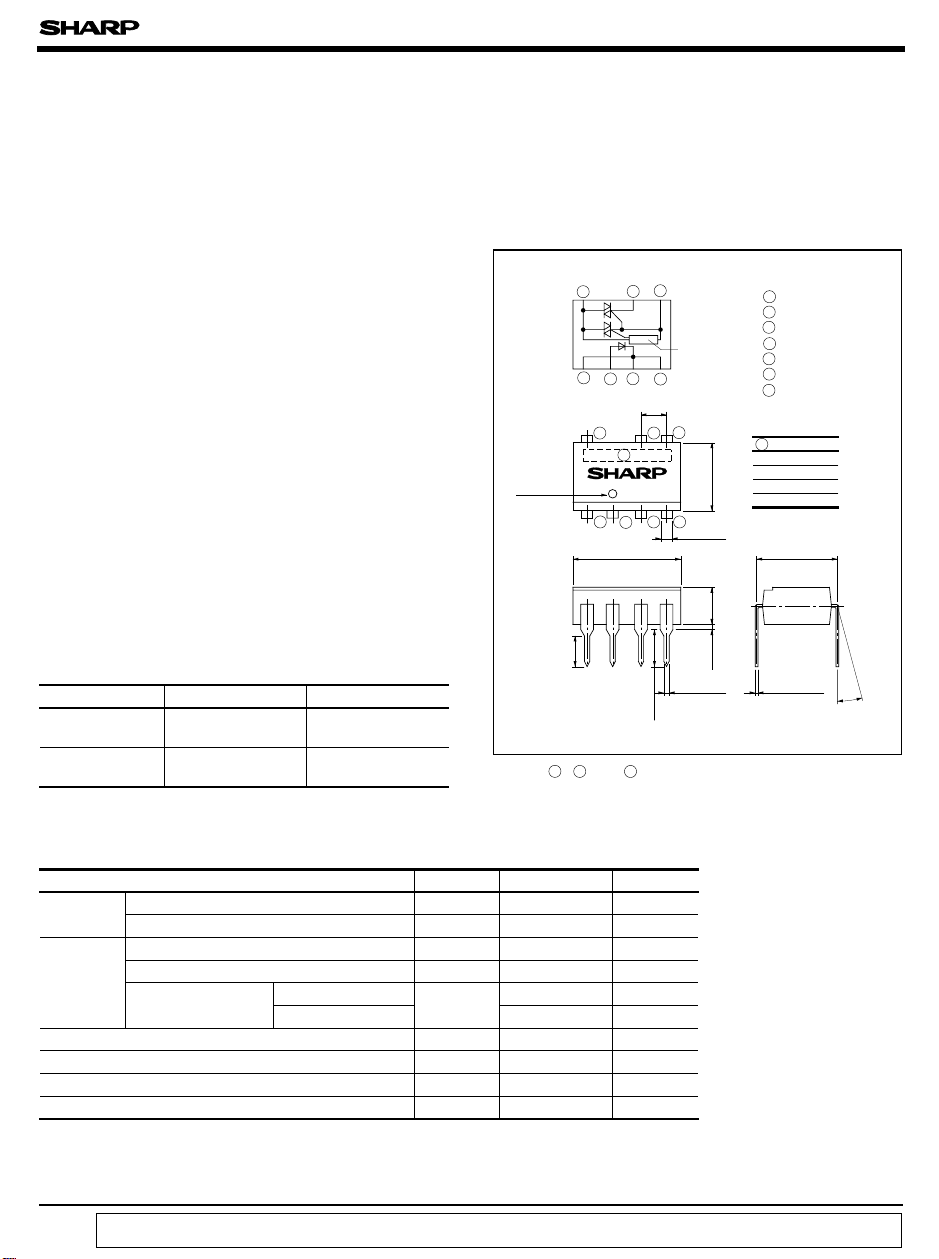
8-Pin DIP Type SSR for Low
Power Control
■ Outline Dimensions
Internal connection Diagram
568
❈
Zero-cross
2.54
±
circuit
±
0.25
568
0.5
±
6.5
±
0.3
1.2
0.5
0.5
±
3.5
TYP.
0.5
±
0.1
0.5
0.5
±
3.4
1234
Anode
mark
1A234
9.66
0.5
±
3.1
❈ Zero-cross circuit for S16MD02 and S26MD02
Terminal 1 , 3 and 4 are common ones of cathode.
To radiate the heat, solder all of the lead pins
on the pattern of PWB.
(
Unit : mm
1 Cathode
2 Anode
3 Cathode
4 Cathode
5 G
6 T
1
8 T
2
A(Model No.
S16MD01
S16MD02
S26MD01
S26MD02
±
0.3
7.62
±
0.1
0.26
θ : 0 to 13˚
)
)
θ
■ Absolute Maximum Ratings
Parameter
Input
Forward current
Reverse voltage
RMS ON-state current
*1
Output
*2
Isolation voltage
Peak one cycle surge current
Repetitive peak OFFstate voltage
S16MD01 /S16MD02
S26MD01 /S26MD02
Operating temperature
Storage temperature
*3
Soldering temperature
*1 50Hz sine wave
*2 AC for 1 minute, 40 to 60%RH, f= 60Hz
*3 For 10 seconds
“ In the absence of confirmation by device specification sheets, SHARP takes no responsibility for any defects that occur in equipment using any of SHARP's devices, shown in catalogs,
data books, etc. Contact SHARP in order to obtain the latest version of the device specification sheets before using any SHARP's device.”
Symbol Rating Unit
I
F
V
R
I
T
I
surge
V
DRM
V
iso
T
opr
T
stg
T
sol
4 000
- 25 to + 80 ˚C
- 40 to + 125 ˚C
(
Ta = 25˚C
50 mA
6V
0.6
6A
400 V
600 V
260 ˚C
)
A
rms
V
rms
S16MD01/S16MD02/S26MD01/S26MD02
■ Electrical Characteristics
Parameter Symbol
Input
Output
Transfer
characteristics
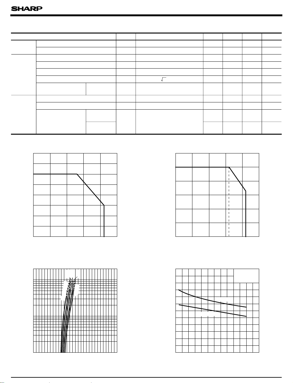
Fig. 1 RMS ON-state Current vs.
Fig. 3 Forward Current vs.
Forward voltage V
Reverse current I
Repetitive peak OFF-state current
ON-state voltage V
Holding current I
Critical rate of rise of OFF-state voltage
Zero-cross voltage
Minimum trigger current I
Isolation resistance R
Turn-on time
Ambient Temperature
0.8
0.7
)
0.6
Arms
(
F
0.5
0.4
0.3
0.2
RMS ON-state current I
0.1
0
- 25 0 25 50 75 100
Forward Voltage
200
100
)
50
mA
(
F
20
10
5
Forward current I
2
Ambient temperature Ta (˚C
=-
a
T
25˚C
50˚C
40
25˚C
25˚C
-
0˚C
S16MD02
S26MD02
S16MD01
S26MD01
S16MD02
S26MD02
80
)
= 20mA - 1.2 1.4 V
I
F
F
=3V - - 10 µA
V
R
R
I
V
DRM
DRM
= 0.6A - - 3.0 V
I
T
T
=6V - - 25 mA
V
D
H
V
dV/dt
Vox
DRM
Resistance load
= 15mA
I
F
V
= 6V, RL= 100 Ω - - 10 mA
D
FT
DC500V, 40 to 60 %RH
ISO
V
= 6V, RL= 100 Ω
D
t
on
= 20mA
I
F
(
Ta= 25˚C
Conditions MIN. TYP. MAX. Unit
= Rated - - 100 µA
=(1/ )• Rated
2
100 - - V/µ s
- - 35 V
10
11
5x10
10
- Ω
- - 100 µ s
--50µs
Fig. 2 Forward Current vs.
Ambient Temperature
60
50
)
mA
(
40
F
30
20
Forward current I
10
0
- 25 0 25 75 100
Ambient temperature T
55 80
50
)
(˚C
a
Fig. 4 Minimum Trigger Current vs.
Ambient Temperature
(
S16MD01/S16MD02
12
)
10
mA
(
FT
8
6
4
Minimum trigger current I
2
S16MD02
S16MD01
)
=6V
V
D
= 100Ω
R
L
)
1
0 0.5 1.0 1.5 2.0 2.5 3.0
Forward voltage VF (V
)
0
- 30 0 20 40 60 80 100
Ambient temperature Ta (˚C
)

S16MD01/S16MD02/S26MD01/S26MD02
Fig. 5 Minimum Trigger Current vs.
Ambient Temperature
12
)
10
mA
(
FT
8
6
4
Minimum trigger current I
2
0
- 30 0 20 40 60 80 100
(
S26MD01/ S26MD02
S26MD01
S26MD02
Ambient temperature Ta (˚C
V
D
= 100 Ω
R
L
)
=6V
Fig. 7 Relative Holding Current vs.
Ambient Temperature
100%
x
)
25˚C
(
H
/ I
)
t˚C
(
H
3
10
2
10
V
D
=6V
Fig. 6 ON-state Voltage vs.
)
Ambient Temperature
1.4
1.3
)
V
(
1.2
T
1.1
1.0
ON-state voltage V
0.9
0.8
- 30 0 20 40 60 80 100
Ambient temperature T
a
(˚C
I
T
)
= 0.6A
Fig. 8 ON-state Current vs.
ON-state Voltage
1.2
I
= 20mA
F
T
= 25˚C
a
1.0
)
mA
0.8
(
T
0.6
0.4
ON-state current I
0.2
1
10
- 30 0 20 40 60 80 100 0 0.5 1.0 1.5
Relative holding current I
Ambient temperature T
a
(˚C
)
0
ON-state voltage VT (V
)
Fig. 9 Turn-on Time vs. Forward Current Fig.10 Turn-on Time vs. Forward Current
100
)
50
µ s
(
40
on
30
20
Turn-ON time t
10
10 20 30 40 50
Forward current I
(
S16MD01
VD=6V
R
T
(mA
F
)
= 100Ω
L
= 25˚C
a
100
)
200
)
100
ms
(
on
50
40
Turn-ON time t
30
20
10 20 30 5040 100
Forward current I
(
S26MD01
V
R
T
(mA
F
D
L
a
)
=6V
= 100Ω
= 25˚C
)

S16MD01/S16MD02/S26MD01/S26MD02
Fig.11 Turn-on Time vs. Forward Current
(
20
)
10
µ s
(
on
5
4
Turn-on time t
3
2
10 20 30 40 50 100
S16MD02/S26MD02
Forward current IF (mA
VD=6V
R
= 100Ω
L
T
= 25˚C
a
)
■ Basic Operation Circuit
R
+ V
CC
V
I
1
D
Tr1
2
8
1
SSR
3
6
)
Load
AC 100V (S16MD01/S16MD02
Z
S
AC 200V (S26MD01/S26MD02
ZS: Surge absorption circuit
Fig.12 Zero-cross Voltage vs.
Ambient Temperature
Load : R
I
= 15mA
F
25
)
V
(
OX
20
Zero-cross voltage V
15
- 30 0 20 40 60 80 100
)
)
(
S16MD02/S26MD02
Ambient temperature T
a
(˚C
)
)
AC supply voltage
Input signal
Load current
(
for resistance load
)
(1)
DC Drive
(2)
Pulse Drive
(3)
Phase Control
Notes 1) If large amount of surge is loaded onto VCC or the driver circuit, add a diode D1 between terminal 2
and 3 to prevent reverse bias from being applied to the infrared LED.
2) Be sure to install a surge absorption circuit.
An appropriate circuit must be chosen according to the load (for CR, choose its constant). This must be
carefully done especially for an inductive load.
3) For phase control, adjust such that the load current immediately after the input signal is applied will be
more than 30mA.
■ Precautions for Use
1) All pins must be soldered since they are also used as heat sinks (heat radiation fins). In
designing, consider the heat radiation from the mounted SSR.
2) For higher radiation efficiency that allows wider thermal margin, secure a wider round
pattern for Pin No.8 when designing mounting pattern. The rounded part of Pin No.5 (gate
must be as small as possible. Pulling the gate pattern around increases the change of being
affected by external noise.
3) As for other general cautions, refer to the chapter“Precautions for Use”
)
 Loading...