

S11MS7
S11MS7
High Speed/ High Noiseresistance Type Phototriac
Coupler
■ Features
1. High speed (ton: MAX. 15 µ s
2. High noise resistance
(dV
: MIN. 500V/ µs
/dt
3. Low trigger current (IFT: MAX. 5mA
4. Mini-flat package type
5. Recognized by UL, file No.E64380
)
)
■ Applications
1. For triggering medium/high power triac
5.3
±
+0.2
-
0.3
0.7
(
Unit : mm
456
+ 0.4
0.5
-
0.2
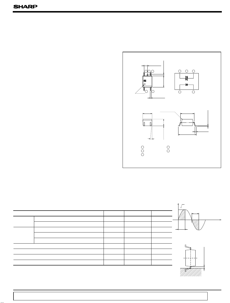
■ Outline Dimensions
±
0.25
1.27
6
)
Anode
mark
45
S11MS
7
13
0.4
±
0.3
3.6
6˚
1 Anode
3 Cathode
4 Anode/
cathode
±
0.1
Input side
Internal connection
diagram
MAX.
0.6
0.2
±
4.4
13
C0.4
0.2
±
2.6
0.1
±
7.0
0.1
5 No external connection
6 Anode/
cathode
0.05
±
)
0.2
θ
■ Absolute Maximum Ratings
Parameter Symbol Rating Unit
Input
Output
Forward current I
Reverse voltage V
∗1
RMS ON-state current I
Peak one cycle surge current I
Repetitive peak OFF-state voltage V
*2
Isolation voltage V
Operating temperature T
Storage temperature T
∗3
Soldering temperature T
F
R
T
0.6 50Hz Sine Wave
surge
DRM
iso
opr
stg
sol
(
Ta = 25˚C
50 mA
6V
0.05
()
400 V
2 500
- 30 to +100
- 40 to +125
)
I
T
(A)
0
A
rms
θ
A
Soldering area
V
rms
˚C
˚C
260 ˚C
2 • I
1
, θ2<= 90˚
1
T
θ
2
180˚
90˚ 360˚
0.2mm or more
∗1 The definition of conduction angle θ of effective on current It should be
as shown in the right drawing.
∗2 40 to 60%RH, AC for 1 minute, f= 60Hz
∗3 For 10 seconds
“ In the absence of confirmation by device specification sheets, SHARP takes no responsibility for any defects that occur in equipment using any of SHARP's devices, shown in catalogs,
data books, etc. Contact SHARP in order to obtain the latest version of the device specification sheets before using any SHARP's device.”
θ
S11MS7
■ Electro-optical Characteristics
Parameter Symbol MIN. TYP. MAX. Unit
Input
Output
Transfer
characteristics
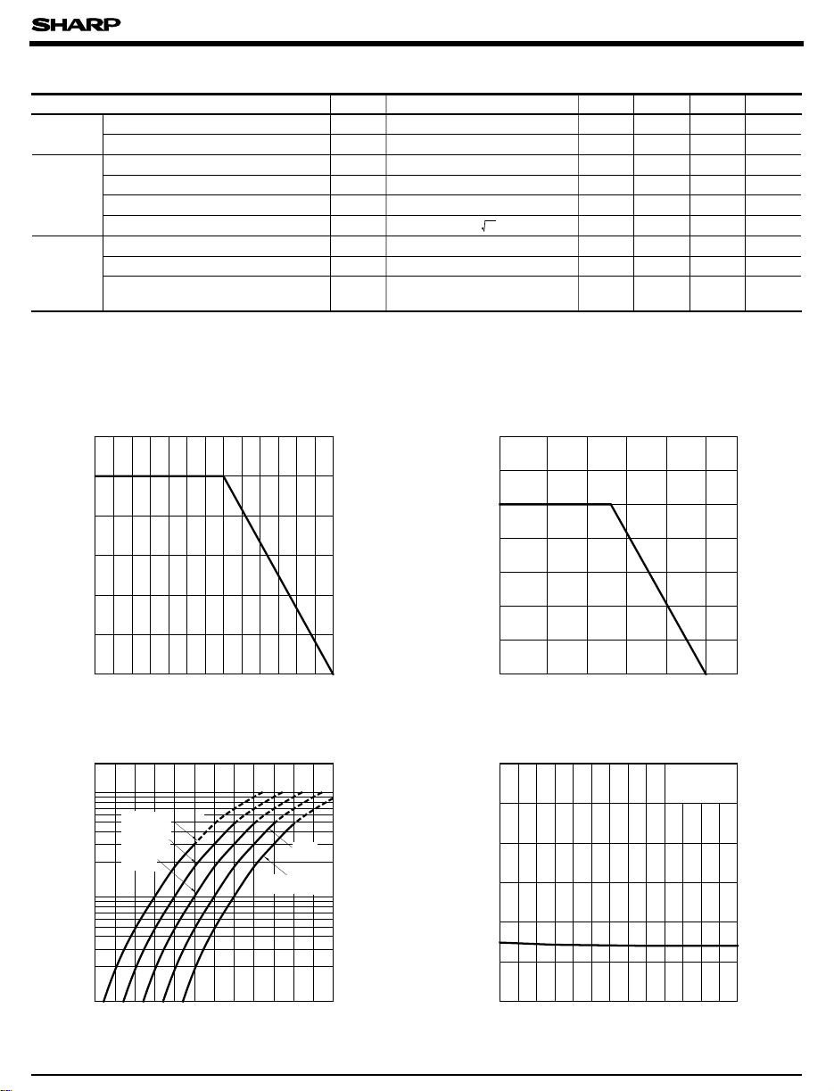
Fig. 1 RMS ON-state Current vs.
Ambient Temperature
Fig. 3 Forward Current vs. Forward Voltage
Forward voltage V
Reverse current I
Repetitive peak OFF-state current
ON-state voltage
Holding current I
Critical rate of rise of OFF-state voltage
Minimum trigger current I
Isolation resistance R
Turn-on time t
60
)
50
rms
mA
(
40
T
30
20
RMS ON-state current I
10
0
-
30 0 50 100
Ambient temperature Ta (˚C
100
50
)
mA
(
F
Forward current I
T
= 75˚C
a
50˚C
20
10
25˚C
5
2
)
0˚C
- 25˚C
F
R
I
DRM
V
T
H
dV/dt
FT
ISO
on
Conditions
= 20mA
I
F
=3V
V
R
= Rated
V
DRM
= 0.05A
I
T
=6V
V
D
V
=(1/ )• Rated
DRM
V
D
2
= 6V, RL= 100Ω
DC = 500V, 40 to 60% RH
VD= 6V, RL= 100Ω ,
= 20mA
I
F
- 1.2 1.4 V
--10µA
--1µA
- 1.3 2.5 V
- 0.5 3.5 mA
500 - - V/µs
--5mA
5x101010
− 10 15 µs
Fig. 2 Forward Current vs.
Ambient Temperature
70
60
)
50
mA
(
F
40
30
20
Forward current I
10
0
-
30
0 25 50 75 100
Ambient temperature T
Fig. 4 Minimum Trigger Current vs.
Ambient Temperature
12
)
10
mA
(
FT
8
6
4
Minimum trigger current I
2
(
Ta= 25˚C
11
- Ω
125
)
(˚C
a
V
=6V
D
R
= 100Ω
L
)
1
0.9
1.0 1.1 1.2 1.3 1.4 1.5
Forward voltage VF (V
0
-
)
30
Ambient temperature Ta (˚C
100500
)

S11MS7
Fig. 5 Relative Repetitive Peak OFF-state
Voltage vs. Ambient Temperature
1.3
)
1.2
= 25˚C
j
1.1
T
(
DRM
1.0
/V
)
a
=T
0.9
j
T
(
0.8
DRM
Relative repetitive peak OFF-state voltage
V
0.7
-
30 0 20406080100
Ambient temperature Ta (˚C
)
Fig. 7 Holding Current vs.
Ambient Temperature
)
mA
(
H
10
1
VD=6V
Fig. 6 ON-state Voltage vs.
Ambient Temperature
2.0
I
= 50mA
T
1.8
)
V
1.6
(
T
1.4
1.2
ON-state voltage V
1.0
0.8
-
30 0 20 100
Ambient temperature Ta (˚C
40 60 80
)
Fig. 8 Repetitive Peak OFF-state Current vs
OFF-state Voltage
- 9
)
(
A
DRM
10
-10
10
Ta= 25˚C
Holding current I
0.1
-
30 100
Ambient temperature T
Fig. 9 Relative Repetitive Peak OFF-state
Current vs. Ambient Temperature
2
10
500
)
(˚C
a
Fig.10 ON-state Current vs.
)
10
= 25˚C
J
T
(
1
DRM
/I
)
a
=T
J
T
-1
(
10
DRM
I
Relative repetitive peak OFF-state current
-2
10
-
30 0 100
●
Please refer to the chapter “Precautions for Use”(Page 78 to 93).
Ambient temperature Ta (˚C
50
)
Repetitive peak OFF-state current I
-11
10
100 200 300 400 500 600
OFF-state voltage V
ON-state Voltage
100
(V
D
IF= 20mA
T
= 25˚C
a
)
mA
(
T
50
ON-state current I
0
0 1.0 2.0
ON-state voltage V
(V
T
)
)
 Loading...