

Sharp S101DH2, S101DH1, S201DH1, S201DH2 Datasheet
16-Pin DIP Type SSR for Low
S101DH1/S101DH2
Power Control
S201DH1/S201DH2
S101DH1/S101DH2/S201DH1/S201DH2
■ Features
1. Compact
(16-pin dual-in-line package type
)
2. High output current
(RMS ON-state current I
: 1.5A
T
3. Built-in zero-cross circuit
(S101DH2/ S201DH2
)
4. Recognised by UL, file No. E94758
5. Approved by CSA, No. LR63705
■ Applications
1. Air conditioners
2. Microwave ovens
3. Home appliances
■ Model Line-ups
No built-in
zero-cross circuit
Built-in zero-cross
circuit
For 100V lines For 200V lines
S101DH1 S201DH1
S101DH2 S201DH2
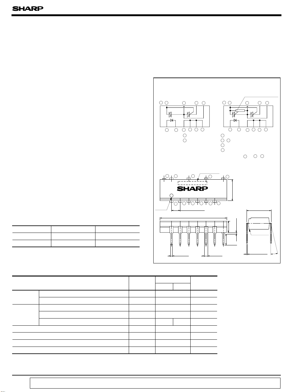
■ Outline Dimensions
Internal connection diagram
S101DH1/S201DH1
16
)
rms
15
2 3 4567
(
Note) To radiate the heat, solder the lead pins
on the pattern of the PWB without using a socket such
that there is no open pin left.
16
15
Anode
234567
mark
0.5
11
13
2 Anode
3 Cathode
13
±
0.25
2.54
19.82
±
0.1
9
Model No.
±
0.5
16
15
11
T
13
9
,
15
Gate
16
NC
11
9
±
0.3
1.2
(
Unit : mm
S101DH2/S201DH2
Zero-cross circuit
11
13
2 3 4567
1
T
2
,
4
to
7
0.5
±
6.5
7.62
0.5
TYP.
±
0.5
3.5
0.5
±
3.4
Epoxy resin
0.26
θ: 0 to 13˚
)
9
9
±
0.3
±
0.1
θ
■ Absolute Maximum Ratings
Parameter
Input
Output
Forward current
Reverse current
RMS ON-state current
Peak one cycle surge
current
Repetitive peak OFFstate voltage
*1
Isolation voltage
Operating temperature
Storage temperature
Soldering temperature
*1 AC for 1 minute, 40 to 60%RH, f=60H
“ In the absence of confirmation by device specification sheets, SHARP takes no responsibility for any defects that occur in equipment using any of SHARP's devices, shown in catalogs,
data books, etc. Contact SHARP in order to obtain the latest version of the device specification sheets before using any SHARP's device.”
Z
Symbol
I
F
V
R
I
T
I
surge
V
DRM
V
iso
T
opr
T
stg
T
sol
Rating
S101DH1/
S101DH2
15 (50HZ, sine wave)A
400 600 V
4,000 V
- 25 to + 85 ˚C
- 40 to + 125 ˚C
260 (For 10 seconds)˚C
(
Ta= 25˚C
S201DH1/
S201DH2
50 mA
6V
1.5 A
)
Unit
rms
rms
S101DH1/S101DH2/S201DH1/S201DH2
■ Electrical Characteristics
Parameter
Input
Output
Transfer
characte
ristics
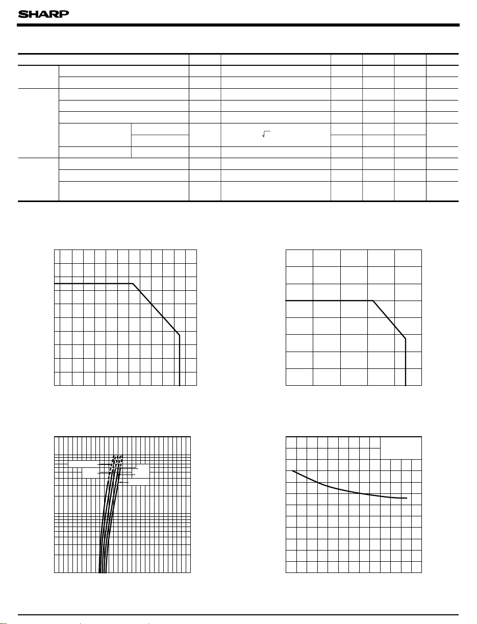
Fig. 1 RMS ON-state Current vs.
Fig. 3 Forward Current vs. Forward Voltage
Forward voltage
Reverse current
Repetitive peak OFF-state current
ON-state voltage
Holding current
Critical rate of rise
of 0FF-state voltage
Zero-cross voltage
Minimum trigger current
Isolation resistance
Turn-on time
Ambient Temperature
2.0
1.8
1.6
)
1.4
Arms
(
T
1.2
1.0
0.8
0.6
0.4
RMS ON-state current I
0.2
0
-
-
25-10
200
100
)
50
mA
(
F
20
10
5
Forward current I
2
01020304050607080
20
Ambient temperature Ta (˚C
Ta= 75˚C
50˚C
-
S101DH1/S101DH2
S201DH1/S201DH2
S101DH2/S201DH2
)
0˚C
25˚C
25˚C
90
Symbol
V
F
I
R
I
DRM
V
T
I
H
dV/dt
V
OX
I
FT
R
ISO
t
on
100
Conditions
= 20mA
I
F
=3V
V
R
= Rated
V
DRM
I
= 1.5A
T
=6V
V
D
V
DRM
Resistance load, I
V
D
2
= 1/ • Rated
F
= 6V, RL= 100Ω
= 15mA
DC500V, 40 to 60%RH
= 6V, RL= 100Ω
V
D
= 20mA
I
F
Fig. 2 Forward Current vs. Ambient
Temperature
80
70
)
60
mA
(
50
F
40
30
Forward current I
20
10
0
- 25 0 25 50 75 100
Fig. 4 Minimum Trigger Current vs.
Ambient Temperature (Typical Value
12
)
10
mA
(
FT
8
6
4
Minimum trigger current I
2
(
MIN. TYP. MAX. Unit
- 1.2 1.4 V
--10µA
- - 100 µ A
- - 1.7 V
- - 25 mA
200 - 100 - -
- - 35 V
--
10
5x10
10
--
Ambient temperature Ta (˚C
11
85
)
(
S101DH1
VD=6V
R
= 100Ω
L
10 mA
- Ω
100
Ta =25˚C
V/µ s
µ s
)
)
)
1
0.50 1.0 1.5 2.0 2.5 3.0
Forward voltage VF (V
0
)
- 30 0 20 40 60 80 100
Ambient temperature Ta (˚C
)
 Loading...