

Page 1
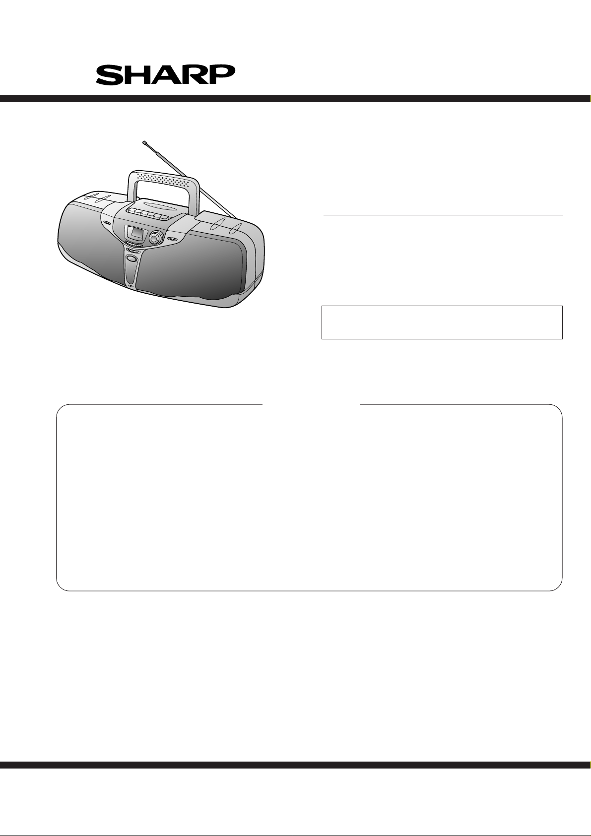
QT-80W
SERVICE MANUAL
No. S4129QT80W///
STEREO RADIO CASSETTE RECORDER
MODEL
• In the interests of user-safety the set should be restored to its
original condition and only parts identical to those specified should
be used.
QT-80W
CONTENTS
Page
SPECIFICATIONS ............................................................................................................................................................. 2
VOLTAGE SELECTION..................................................................................................................................................... 2
AC POWER SUPPLY CORD AND AC PLUG ADAPTOR ................................................................................................. 2
NAMES OF PARTS ........................................................................................................................................................... 3
HOW TO SET THE POINT "0" ON TUNER DIAL MEMORY............................................................................................. 3
DISASSEMBLY.................................................................................................................................................................. 4
REMOVING AND REINSTALLING THE MAIN PARTS..................................................................................................... 5
ADJUSTMENT ................................................................................................................................................................... 7
SCHEMATIC DIAGRAM .................................................................................................................................................. 10
WIRING SIDE OF P.W.BOARD....................................................................................................................................... 12
NOTES ON SCHEMATIC DIAGRAM .............................................................................................................................. 14
TYPES OF TRANSISTOR ............................................................................................................................................... 14
VOLTAGE ........................................................................................................................................................................ 14
PARTS GUIDE/EXPLODED VIEW
SHARP CORPORATION
This document has been published to be used
for after sales service only.
The contents are subject to change without notice.
Page 2
QT-80W
FOR A COMPLETE DESCRIPTION OF THE OPERATION OF THIS UNIT, PLEASE REFER
TO THE OPERATION MANUAL.
General
Power source
Power consumption
Output power
Speakers
Output terminal
Input terminals
Dimensions
Weight
Radio
Frequency range
Tape recorder
Frequency response
Signal/noise ratio
Wow and flutter
Motor
Bias system
Erase system
SPECIFICATIONS
AC 110-127/220-240 V, 50/60 Hz
DC 12 V [“D” size (UM/SUM-1, R20 or HP-2) battery x 8]
20 W
MPO: 18 W (9 W + 9 W) (AC operation, 10 % T.H.D)
RMS: 10 W (5 W + 5 W) (DC operation, 10 % T.H.D)
8 cm (3-1/8”) full range speaker x 4
Headphones: 16-50 ohms (recommended: 32 ohms)
Mixing microphone: 600 ohms
Line input: 350 mV/47 kohms
Width: 520 mm (20-1/2”)
Height: 191 mm (7-1/2”)
Depth: 216 mm (8-1/2”)
4.2 kg (9.3 lbs.) without batteries
FM: 88 - 108 MHz
SW1: 2.3 - 7.3 MHz
SW2: 7.3 - 22 MHz
MW: 526.5 - 1,606.5 kHz
60 - 12,000 Hz (Normal tape)
40 dB
0.3 % (WRMS)
DC 9 V electric governor
AC bias
Magnet erase
Specifications for this model are subject to change without prior notice.
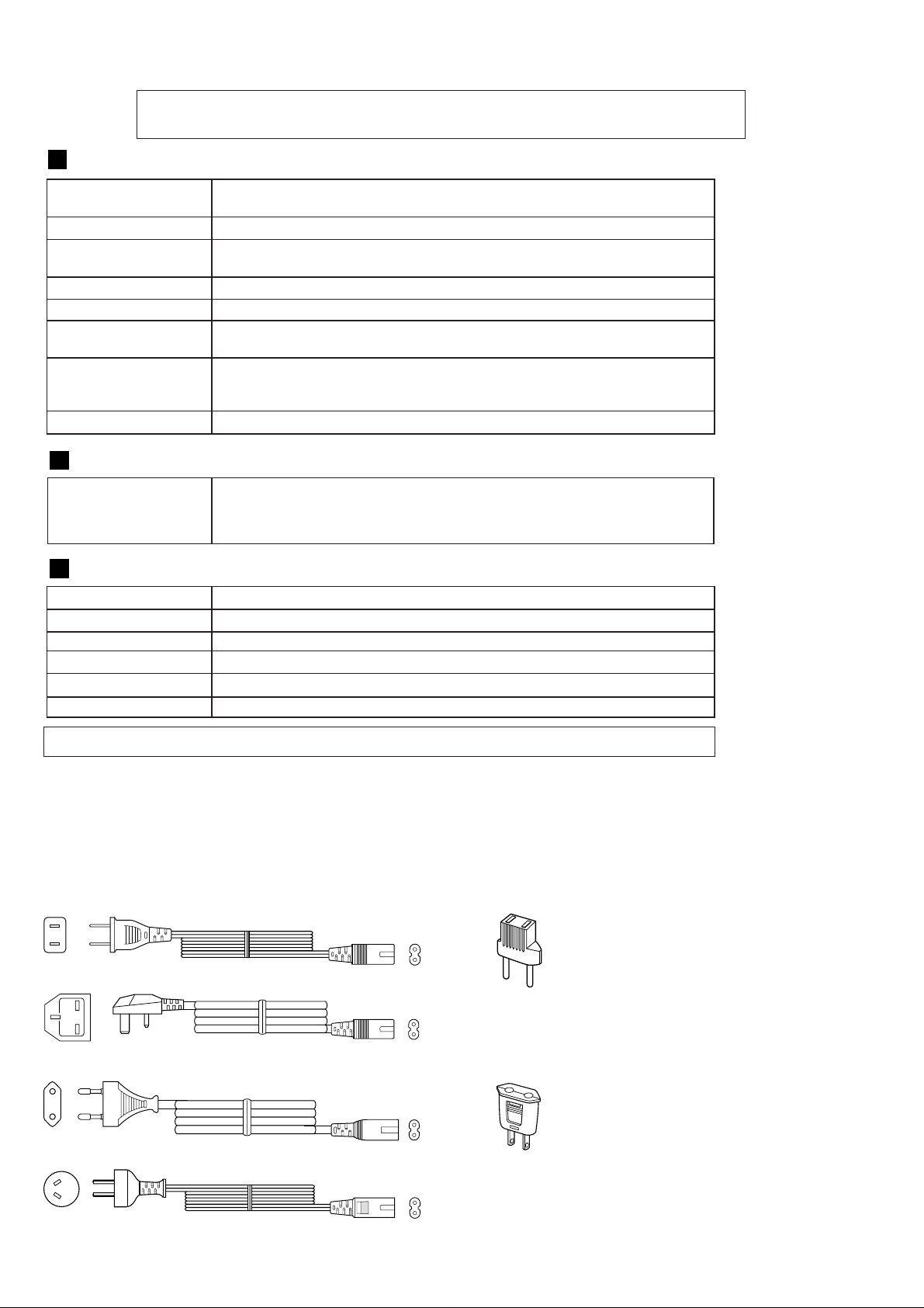
VOLTAGE SELECTION
Before operating the unit on mains, check the preset voltage. If the voltage is different from your local voltage, adjust the voltage
as follows. Slide the selector with a screwdriver to the appropriate voltage number. (AC 110 - 127 V or AC 220 - 240 V)
AC POWER SUPPLY CORD AND AC PLUG ADAPTOR
92L3404-074001
QACCB0012AW00
QACCE0007AW00
QACCL0002AW00/QACCL0008AW00
QPLGA0003AWZZ
QPLGA0004AWZZ
– 2 –
Page 3
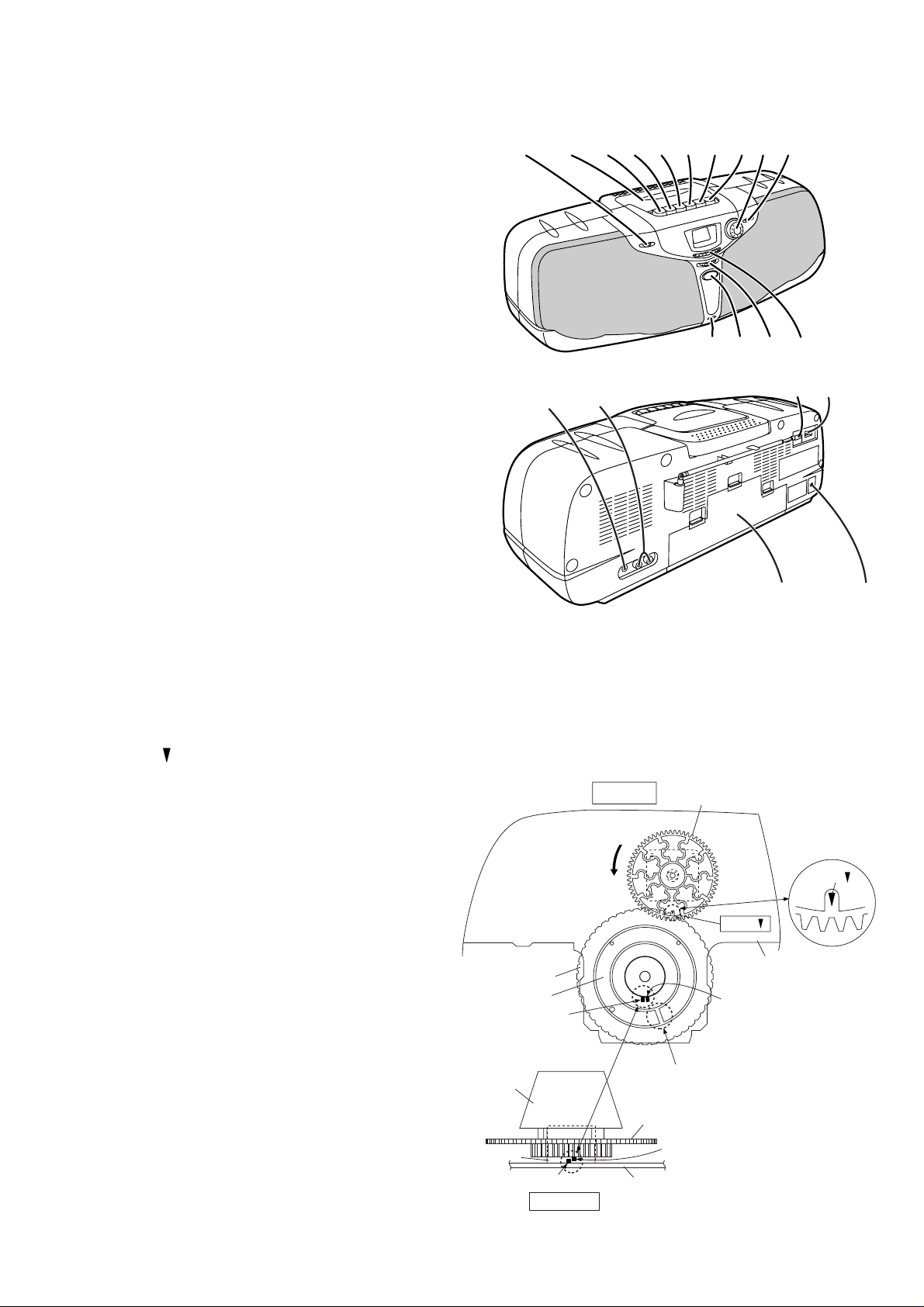
NAMES OF PARTS
QT-80W
01. Function/Beat Cancel Switch
02. Cassette Compartment
03. Record Button
04. Play Button
05. Rewind Button
06. Fast Forward Button
07. Stop/Eject Button
08. Pause Button
09. Volume Control
10. Band Selector
11. Built-in Microphone
12. Extra Bass Button
13. Fine Tuning Control
14. Tuning Control
15. Mixing Microphone Socket
16. Line Input Sockets
17. AC Voltage Selector
18. AC Input Socket
19. Battery Compartment
20. Headphone Socket
12345678910
15
11 12 13
16
14
17
18
HOW TO SET THE POINT "0" ON TUNER DIAL MEMORY
1. Remove the front cabinet and main PWB. (Refer to page 4,
of disassembly section.)
2. Turn the gear dial in the arrowed direction until it stops so
that the " " mark comes to the front of main PWB.
3. When the tuning knob is set at 2, adjust it from above so that
its "0" point rib comes to the right of "0" point rib of the dial
drum when you face the unit.
4. Check the tuning display label by turning the tuning knob.
The frequency band will be FM 88 - 108 MHz when the dial
is turned counter-clockwise.
5. Reassemble the front cabinet.
Tuning Knob
Dial Drum
Dial Drum “0”
Point Rib
Top Side
2
19
Gear Dial
Mark “ ”
Main PWB Front Side
Tuning Knob “ 0 ” Point Rib
20
Mark “ ”
Dial Drum
Tuning Knob
Bracket
Dial Drum “0” Point Rib
– 3 –
Front Side
“0” Point of Tuning Display
3
Tuning Knob
Tuning Knob “0” Point Rib
Main PWB
Figure 3
Page 4
QT-80W
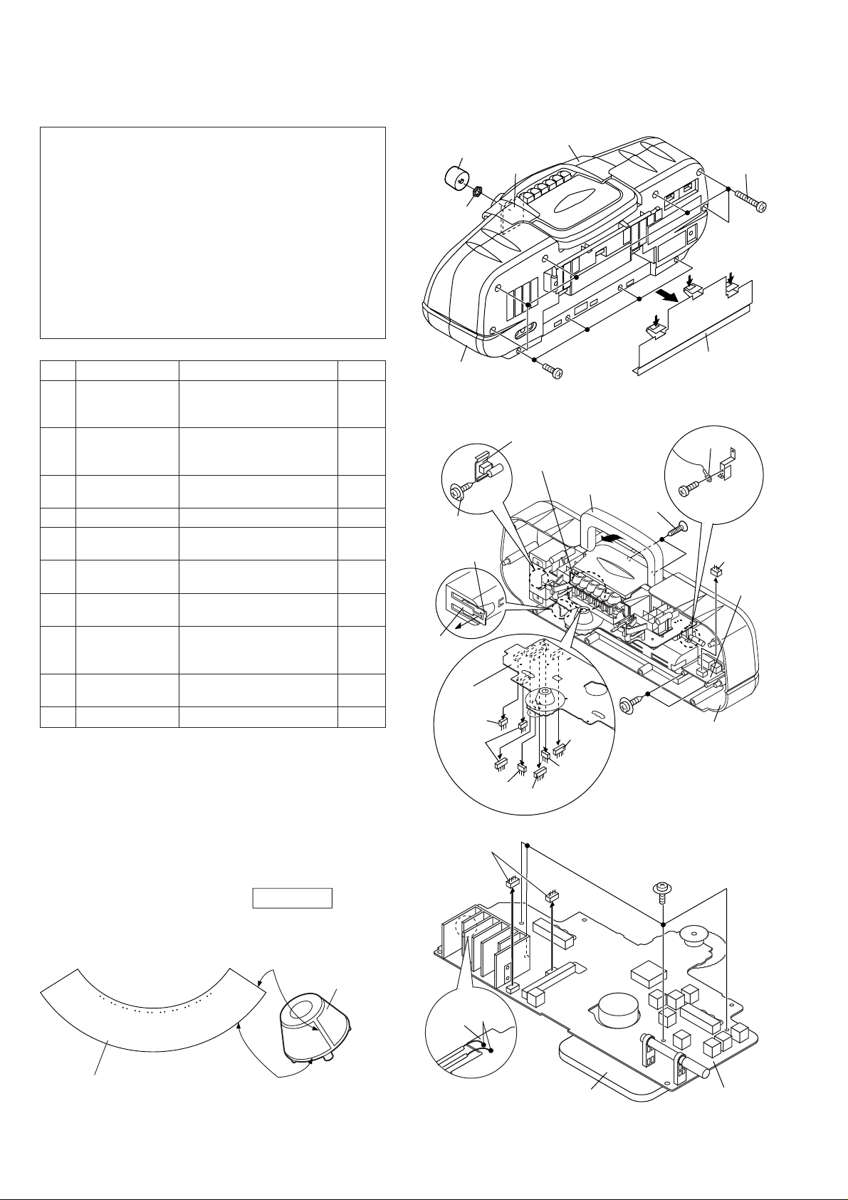
DISASSEMBLY
Caution on Disassembly
Follow the below-mentioned notes when disassembling the
unit and reassembling it, to keep it safe and ensure excellent
performance:
1. Take cassette tape out of the unit.
2. Be sure to remove the power supply plug from the wall
outlet before starting to disassemble the unit.
3. Take off nylon bands or wire holders where they need to
be removed when disassembling the unit. After servicing
the unit, be sure to rearrange the leads where they were
before disassembling.
4. Take sufficient care on static electricity of integrated
circuits and other circuits when servicing.
STEP REMOVAL PROCEDURE FIGURE
1 Rear Cabinet 1. Battery Lid............ (A1) x1 4-1
2. Screw ................... (A2) x6
3. Screw ................... (A3) x4
2 Front Cabinet 1. Knob..................... (B1) x1 4-1
2. Nut........................ (B2) x1
3. Socket .................. (B3) x3 4-2
3 Jack PWB 1. Socket ..................(C1) x2 4-2
2. Screw ...................(C2) x2
4 Volume PWB 1. Socket ..................(D1) x1 4-2
5 Battery PWB 1. Socket .................. (E1) x1 4-2
2. Hook..................... (E2) x1
6 Headphones PWB 1. Socket .................. (F1) x1 4-2
2. Screw ................... (F2) x1
7 Main PWB with 1. Screw ...................(G1) x2 4-2
Tape Mechanism 2. Screw ...................(G2) x1
8 Main PWB 1. Socket ..................(H1) x2 4-3
2. Screw ...................(H2) x4
3. Solder................... (H3) x2
9 Tape Mechanism 1. Open the cassette holder. 5-1
2. Screw ....................(J1) x4
10 X-BASS PWB 1. Screw ................... (K1) x3 5-2
(B1)x1
(B2)x1
Rear Cabinet
(F2)x1
ø4x10mm
Battery PWB
(E2)x1
Main PWB
(C1)x1
(B3)x2
Front Cabinet
Volume
PWB
(A3)x4
ø3x12mm
Figure 4-1
Headphones PWB
Tape Mechanism
Handle
(D1)x1
(G1)x2
ø3x12mm
(C2)x2
ø4x14mm
(A2)x6
ø3x30mm
(A1)x1
Lug Wire
(G2)x1
ø3x8mm
(B3)x1
Jack
PWB
Rear
Cabinet
How to attach the tuning display label
(See Fig. 4-4.)
Reference
1. Start Stick Label Matching
With Base Line
Base Line
10
108
1600
9
22.0
7.3
19.0
1400
6.0
104
1200
5.0
15.0
8
7
6
5
100
1000
800
4.0
12.0
Tuning Display Label
96
4
3.2
10.0
700
0
1
88
2
3
540
92
2.3
7.3
600
2.6
8.5
2. This Line Must Be
Stick Matching
Figure 4-4
Dial Drum
– 4 –
Main
PWB
(C1)x1
(F1)x1
(H1)x2
(H3)x2
Tape Mechanism
(E1)x1
Figure 4-2
(H2)x4
ø3x10mm
Main PWB
Figure 4-3
Page 5
QT-80W
Tape Mechanism
Stop/Eject Button
Push
Cassette
Holder
Open
(J1)x4
ø3x10mm
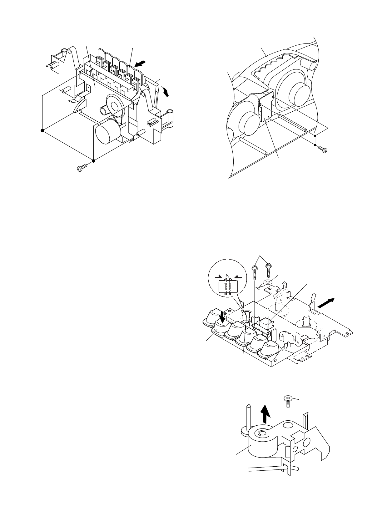
REMOVING AND REINSTALLING THE MAIN PARTS
TAPE MECHANISM SECTION
Perform steps 1 to 9 of the disassembly method to remove the
tape mechanism. (See page 4.)
Front Cabinet
X-BASS
Figure 5-2Figure 5-1
(K1)x3
ø2.6x8mm
PWB
How to remove the record / playback and erase
heads (See Fig. 5-3.)
1. Remove the screws (A1) x 2 pcs., to remove the record/
playback head.
2. Remove the hooks (A2) x 2 pcs., toward the center position
as shown in Fig. 5-3. and then extract the erase head
upward.
Note:
After replacing the heads and performing the azimuth
adjustment, be sure to apply screwlock.
How to remove the pinch roller (See Fig. 5-4.)
1. Remove the screw (B1) x 1 pc., and remove the pinch roller
upwards.
Push
PLAY
Button
Hook
(A2)x2
Erase Head
(A1)x2
ø2x7mm
Lug Wire
Record/Playback
Head
Figure 5-3
(B1)x1
ø1.5x2.5mm
– 5 –
Pinch Roller
Figure 5-4
Page 6
QT-80W
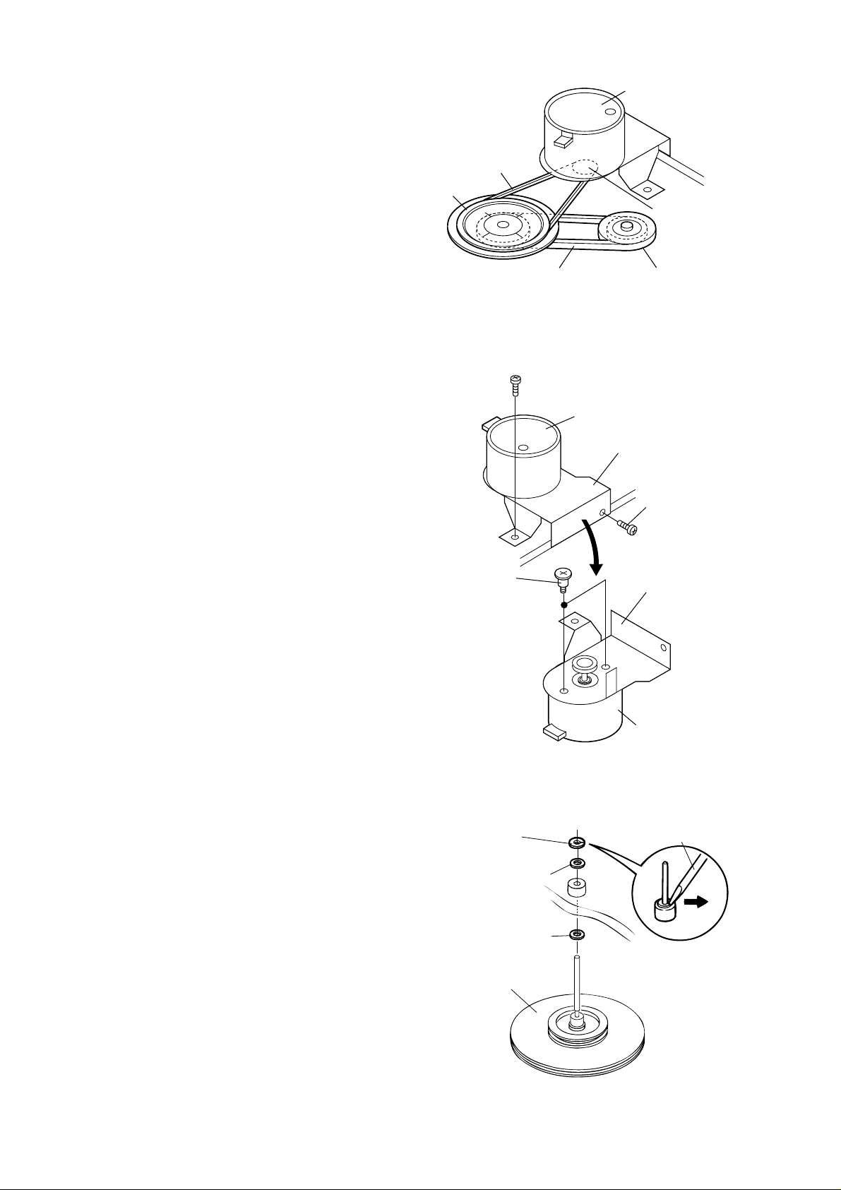
How to remove the belts (See Fig. 6-1.)
1. Remove the main belt (C1) x 1 pc., from the motor pulley.
2. Remove the FF/REW belt (C2) x 1 pc., from the REW/FF
roller.
3. Put on the belts in the reverse order of removal.
Note:
When putting on the belt, ascertain that the belt is not twisted,
and clean it.
How to remove the motor
(See Fig. 6-2.)
1. Remove the main belt. (See Fig. 6-1.)
2. Remove the screws (D1) x 2 pcs., to remove the motor
bracket.
3. Remove the screws (D2) x 2 pcs., to remove the motor.
Note:
When mounting the motor, pay attention to the motor bracket
angle.
Main Belt
(C1)x1
Flywheel
FF/REW Belt
(C2)x1
Figure 6-1
(D1)x1
ø2x4mm
Motor
Motor
Motor Pulley
REW/FF
Roller
Motor Bracket
(D1)x1
ø2x4mm
How to remove the flywheel (See Fig. 6-3.)
1. Remove the belt. (See Fig. 6-1.)
2. Remove the stop washer (E1) x 1 pc., with a small precision
screwdriver to extract the flywheel from the capstan metal.
Note:
When the stop washer is deformed or damaged, replace it
with a new one.
(D2)x2
ø2.6x1.6mm
Special Screw
(E1)x 1
Stop Washer
Washer
Washer
Flywheel
Motor Bracket
Motor
Figure 6-2
Driver
How to reinstall the parts
Install each part in the reverse order of the removal with care.
Figure 6-3
– 6 –
Page 7

ADJUSTMENT
TUNER SECTION
fL: Low-range frequency
fH: High-range frequency
FM Section
Step
1 FM IF: (1) FM IF sweep Inject the IF Signal are taken Adjust T106, T108 (1) Band SW in FM.
2 FM BAND (1) FM RF sweep Inject the RF Same as step 1 Adjust P.V.C. (TC1) Same as step 1
3 FM BAND Same as step 2 Same as step 2 Same as step 1 Adjust L103 to get Tune P.V.C. to low
4 Repeat step 2, 3 until no further improvement can be made.
5 FM TRACKING Same as step 2 Same as step 2 Same as step 1 Adjust P.V.C. (TC2) to Tune P.V.C. to
6 FM TRACKING Same as step 2 Same as step 2 Same as step 1 Adjust L102 to get MAX. Tune P.V.C. to
7 Repeat step 5, 6 and then step 2, 3, 5, 6 until no further improvement can be made.
Alignment
Frequency
10.7 MHz generator sweep signal out from point TP3 and repeat to get (2) VOL. & TONE
(T108) (2) Alignment through 300 pF best "S" curve with control in MIN.
FM oscilloscope capacitor to point center at 10.7 MHz position
DETECTION: (3) Power supply TP2 (3) Tune P.V.C. to
(T106) high end
COVERAGE fH: generator signal directly to get MAX. output
108.2 MHz (2) Alignment point TP1
COVERAGE fL: MAX. output end
87.4 MHz
fH: 106 MHz get MAX. output 106 MHz
fL: 90 MHz output 90 MHz
Test Equipment
oscilloscope
(3) Power supply
Signal-in
Signal-out
Adjust
QT-80W
Remark
FM Stereo Section
Step
1 VCO: 75 kHz (1) Frequency counter Inject MONO Through test Adjust VR102 let (1) FM and stereo
Alignment
Frequency
Test Equipment
(2) Power supply signal at 98 MHz circuit as Fig 7. Frequency counter position
(3) FM Signal directly to point value: 76 K ± 200 Hz. (2) Tune radio to
generator TP1 and ground 98 MHz
Pin 13 of IC102
Signal-in Signal-out
Pin 21 of IC102
Adjust
Remark
D
G
FET 2SK212
(or other 2SK type FET)
10pF
S
1M ohm
0.1
F
To frequency
counter
10K ohm
Figure 7
– 7 –
Page 8

QT-80W
MW Section
Step
1 MW IF: 455 kHz (1) AM IF sweep Let the MW ANT Take out the signal Adjust T107 get MAX. (1) Band SW in MW
2 MW (1) MW sweep Same as step 1 Same as step 1 Adjust P.V.C. (TC3) Same as step 1
3 MW BAND Same as step 2 Same as step 1 Same as step 1 Adjust T103 to get Tune P.V.C. to low
4 Repeat step 2, 3 until no further improvement can be made.
5 MW BAND Same as step 2 Same as step 1 Same as step 1 Adjust P.V.C. (TC4) Tune P.V.C. to
6 MW TRACKING Same as step 2 Same as step 1 Same as step 1 Adjust L109 get MAX. Tune P.V.C. to
7 Repeat step 5, 6 and then step 2, 3, 5,6 until no further improvement can be made.
Alignment
Test Equipment
Signal-in
Signal-out Adjust
Frequency
generator with coil close to the from point TP4 output at 455 kHz position
loop antenna generator ANT. (2) VOL. control in MIN.
(2) Alignment position
oscilloscope (3) Tune P.V.C. to
(3) Power supply high end
TRACKING fH: generator with get MAX. output at
1,650 kHz antenna 1,650 kHz
(2) Alignment
oscilloscope
(3) Power supply
COVERAGE fL: MAX. output at 515 kHz end
515 kHz
COVERAGE fH: get MAX. output at 1.400 kHz
1,400 kHz 1,400 kHz
fL: 600 kHz output at 600 kHz 600 kHz
Remark
SW1 Section
Step
1 SW1 BAND (1) SW1 sweep Let the MW ANT Take out the signal Adjust CT102 get MAX. (1) Band SW in SW1
2 SW1 BAND Same as step 1 Same as step 1 Same as step 1 Adjust T104 get MAX. Tune P.V.C. to low
3 Repeat step 1, 2 until no further improvement can be made.
4 SW1 Same as step 1 Same as step 1 Same as step 1 Adjust CT104 get MAX. Tune P.V.C. to 6 MHz
5 SW1 Same as step 1 Same as step 1 Same as step 1 Adjust T101 get MAX. Tune P.V.C. to
6 Repeat step 4, 5 and then step 1, 2, 4, 5 until no further improvement can be made.
Alignment
Test Equipment
Signal-in Signal-out Adjust Remark
Frequency
COVERAGE fH: generator with coil close to the from point TP4 output at 7.4 MHz position
7.4 MHz antenna generator ANT. (2) VOL. control in MIN.
(2) Alignment point TP1 position
oscilloscope (3) Tune P.V.C. to
(3) Power supply high end
COVERAGE fL: output at 2.25 MHz end
2.25MHz
TRACKING fH: output at 6 MHz
6 MHz
TRACKING fL: output at 2.6 MHz 2.6 MHz
2.6 MHz
SW2 Section
Step
1 SW2 BAND (1) SW2 sweep Inject the RF Take out the signal Adjust CT101 get MAX. (1) Band SW in SW2
2 SW2 BAND Same as step 1 Same as step 1 Same as step 1 Adjust T105 get MAX. Tune P.V.C. to low
3 Repeat step 1, 2 until no further improvement can be made.
4 SW2 Same as step 1 Same as step 1 Same as step 1 Adjust CT103 get MAX. Tune P.V.C. to
5 SW2 Same as step 1 Same as step 1 Same as step 1 Adjust T102 get MAX. Tune P.V.C. to
6 Repeat step 4, 5 and then step 1, 2, 4, 5 until no further improvement can be made.
Alignment
Frequency
COVERAGE fH: generator signal directly to from point TP4 output at 22.5 MHz position
22.5 MHz (2) Alignment point TP1 (2) VOL. control in MIN.
Test Equipment Signal-in
Signal-out
Adjust
Remark
oscilloscope position
(3) Power supply (3) Tune P.V.C. to
high end
COVERAGE fL: output at 7.2 MHz end
7.2 MHz
TRACKING fH: output at 19 MHz 19 MHz
19 MHz
TRACKING fL: output at 8.5 MHz 8.5 MHz
8.5 MHz
– 8 –
Page 9

Erase Head
Head fixing
screw
Record/
Playback
Head
Tape Mechanism
MAIN PWB
QT-80W
MW BAR ANTENNA
MW
TRACKING fL
ROD
ANTENNA
L109
FM
DETECTION
T103
CT102
T104
T105
VCO
VR102
T106
MW BAND
COVERAGE fL
fH
SW1 BAND
COVERAGE
fL
fL
CT101
fH
TP3
13
17
18
21
24
TP4
SW1
TRACKING
SW2 BAND
COVERAGE
12
IC102
1
TP1
fH
fL
MW IF
T107
CT104
T102
T108
FM IF
T101
CT103
fH
SW2
TRACKING
fL
TP2
IC101
9
8
L103
TC1
TC3
MW
TRACKING fH
fL
FM BAND
COVERAGE
fH
1
TC2
TC4
TUNER P.V.C.
BIAS
OSCILLATION
TP5
IC201
L102
fL
fH
MW BAND
COVERAGE fH
T201
C216
FM
TRACKING
S201
RECORD/PLAYBACK
MECHANISM SECTION
Step
1 Head Playback test tape Connect VTVM and oscilloscope to Head fixing screw Adjust to get MAX.
2 Bias Frequency Record position Connect frequency counter to TP5 and Adjust T201 80 kHz ± 1 kHz
3 Beat cancel Record position Same as step 3 S201 from playback 75 kHz ± 0.5 kHz
BIAS
OSCILLATION
TP5
Item
adjustment MTT-113 6.3 kHz speaker output (see Fig 9-3.) audio output
adjustment ground (Bias Oscillation)
T201
C216
IC201
S201
REC
Condition
1
2
3
4
CON504
M601
TAPE
MOTOR
CON201
1
2
3
4
RECORD/PLAYBACK
PLAY
BACK
CN201
Figure 9-1 ADJUSTMENT POINTS
TAPE Section
Connection Adjust
SW601
TAPE MAIN
4
3
2
1
CN504
1
2
3
4
RECORD/
PLAYBACK HEAD
TAPE
Output
to record
MAIN PWB
ERASE HEAD
Figure 9-2 ADJUSTMENT POINTS
Figure 9-3
– 9 –
Page 10

QT-80W
A
B
C
D
E
F
G
H
ROD
ANTENNA
JK201
MIXING
MICROPHONE
MIC
BUILT-IN
MICROPHONE
JK301
LINE INPUT
RECORD/
PLAYBACK
HEAD
L-CH
TAPE
R-CH
ERASE HEAD
SELECTOR
TP1
S101-C
VD101
1S2638
C116
0.02
C117
0.02
R108
22K
VR101
100K(B)
FINE TUNING
CON203
CN203
2
L-CH
R-CH
S101
BAND
FM
MW
SW1
SW2
R106
100K
R107
100K
C115
R109
22K
JACK
PWB-A2
R240
1K
R234
4.7K
2
C227
11
10/16
GND
4
4
3
3
2
2
1
1
CN201
CON201
RECORD/PLAYBACK
BP101
BAND PASS
FILTER
88-108MHz
1
S101
BAND
SELECTOR
S101-F
VC4
S101-D
5P
VC3
SELECTOR
R
S201-C
P
R
S201-H
P
S201
2
5
1
3
1
S101
BAND
C101
0.001
3
FM
MW
SW1
SW2
FM
MW
SW1
SW2
CN202
5
4
3
2
1
3
2
1
CN301
0.0022(ML)
R212
18K
C212
0.0022(ML)
C223
100P
22P(CH)
L102
FM RF
C102
0.001
C111
300P
C113
1500P
C114
0.0047
CON202
5
4
3
2
1
3
GND
2
1
CON301
C211
R211
18K
R250
18K
TP5
Q208
2SC945
1
C106
C141
10P
CT104
10P
CT103
10P
C112
5P
CT102
10P
CT101
10P
C118
0.22
SWITCHING
R242
10K
R301
R303
10K
C216
0.0027
2
C104
R122
10
R124
Q204
SS8550
10K
RPR
RECORD/
PLAYBACK
RPR
OSCILLATION
R254
10K
3
0.001
TC4
33K
S201
R253
10K
IC101
FM FRONT END
LA1186N
4
5
C143
0.1
D103
TC2
VC2
1N4148
C103
10/16
L109
MW BAR ANTENNA
T101
SW1 ANTENNA
T102
SW2 ANTENNA
TC3
T103
MW OSCILLATION
T104
SW1 OSCILLATION
T105
SW2 OSCILLATION
C235
47/16
C270
10/16
C231
1/50
C230
1.8K
R233
0.01(ML)
R302
2.2K
R304
2.2K
S201-E
S201-D
P
C201
0.0015(ML)
S201-A
S201-B
P
T201
C251
0.018
(ML)
BIAS
0.0068(ML)
FM(MONO)/BEAT
TAPE(STAND-BY)
6789
TP2
T108
FM IF
C139
0.02
R110
100
R111
47
R112
47
C119
0.22
R237
4.7K
R256
680K
Q207
2SC945
MIXING MIC
PRE AMP.
C209
0.001(ML)
IC201
BA3313L
R202
3.9K
C204
C202
47/16
0.0015(ML)
150
R204
R201
3.9K
120K
R231
BIAS OSC.
R225
3DA8050
22K
C220
C219
0.022
LINE
S301-E
FM(ST)
BEAT CANCEL
L103
TC1
L102
TC2
R102
33
S101
BAND
SELECTOR
FM
MW
SW1
SW2
C121
0.22
FM
MW
SW1
SW2
SELECTOR
R241
330
C233
39K
R215
OUT1
2 3 4
1
5.6K
R208
C206
0.022(ML)
Q201
(ML)
S301
FUNCTION/
C107
15P
(CH)
R101
47
S101-E
S101-A
S101
BAND
1/50
R222
C210
0.001
ALC
C213
L103
10/16
22K
+B
fH
C120
(ML)
NF1
47/16
C218
47/16
R247
fL
fH
fL
FM OSC.
C258
330P
C208
0.47/50
220
FM BAND
COVERAGE
FM
TRACKING
C108
20P
(CH)
C138
220/16
CF101
10.7MHz
FM IF
22K
R223
R217
330K
R218
330K
39K
R216
IN1
N.C.
5
C259
0.0027
470K
R213
C207
0.47/50
R105
fL
T103
MW BAND
COVERAGE
fH
TC4
fL
L100
MW
TRACKING
fH
TC3
C109
R103
5P
220K
C142
0.02
TC1
VC1
0.22
C137
T106
FM
100
DETECTION
C145
100/16
24
AM
FM IF
1
1
2
PLAYBACK/RECORD
PRE AMP. & CONTROL
GND
6 7
C214
220/16
P
S201-G
R
R224
10
21
23
22
STB
OSC
AM RF
AM MIX
2 3 4 5 6
3
0.02
C123
T107
MW IF
CF102
AM IF
C122
0.02
+B
22K
22K
R243
R244
IC201
BA3313L
FILTER
VCC
IN2
GND
8
9
R214
100
1/50
C257
C260
0.0027
C215
0.022(ML)
R232
120K
R209
1K
P
S201-I
R
S201
RECORD/
PLAYBACK
+VCC
AGC
10
C261
330P
R210
C110
0.02
R121
AM IF
C124
1
S301-B
+B
R207
R219
27K
1K
3.9K
22/16
CT102
T104
T101
CT104
R104
820K
C136
0.0047
(ML)
2.7K
R120
TP4
IC102
FM DET
LA1805
7
C125
0.015(ML)
C126
0.015
3
2
TAPE(STAND-BY)
FM(ST)
FM(MONO)/BEAT
LINE
S301
FUNCTION/
BEAT CANCEL
NF2
OUT2
12
11
D201
1N4148-T72
C203
R251
47/16
5.6K
R203
150
R220
27K
C518
fL
fH
fL
fH
C135
TP3
0.0082(ML)
17181920
DET
OUT
AM IN
GNDGND
8 9 10 11
(ML)
1/50
C127
R113
R114
2.2K
R116
2.2K
18K
S201-F
3DA8050
+B
0.1
C516
220/16
SW1 BAND
COVERAGE
SW1
TRACKING
S301
FUNCTION/
BEAT CANCEL
R118
100K
470P
C134
C133
3.3/50
C132
15
16
IN
MPX
IF AD
L-CH
R-CH
1/50
C128
10K
R115
R
S201
P
RECORD/PLAYBACK
Q501
T105
CT101
T102
CT103
S301-F
R119
C131
1500P
3.3/50
13
14
FM IF DET./
VCO
MO/ST
MW/SW MIXER
N.C.
AM/
FM
12
SW2
SW1
R117
10
MW
FM
1/50
C129
10K
LINE
FM(MONO)/
BEAT
FM(ST)
TAPE
(STAND-BY)
FM(MONO)/BEAT
FM(ST)
TAPE(STAND-BY)
+B
R501
560
ZD501
TZX8V2 C
fL
SW2 BAND
COVERAGE
fH
fL
SW2
TRACKING
fH
LINE
FM(MONO)/BEAT
FM(ST)
TAPE(STAND-BY)
VR102
10K(B)
VCO
15K
IC102
LA1805
S101-B
S101
BAND
SELECTOR
R123
100
S301-C
S301
FUNCTION/
BEAT CANCEL
C303
0.047(ML)
C304
0.047(ML)
LINE
S301-D
S301
FUNCTION/
BEAT CANCEL
SW601
TAPE MAIN
PLAY
M
M601
TAPE
MOTOR
+9V
+B
3
2
1
4
3
2
1
CON302
CN504
• NOTES ON SCHEMATIC DIAGRAM can be found on page 14.
1
2
34 5
Figure 10 SCHEMATIC DIAGRAM (1/2)
– 10 –
6
Page 11

78 9101112
1
5
3
FM IF
MIX
RF AMP
22
RNG.
23
OSC
24
LEVEL DET
AM IF
GND
6
IC BLOCK DIAGRAM
12
17
POST
AMP.
MUTING
TUNING
INDIC.
DRIVE
16
19
8
20
2
DCT
DET
AGC
4
IC101: LA1186N
VRE1
RF
1 2
MIX
3
4
QT-80W
Vcc
OUT 1
33K
47µ
47µ
NF 1
IN 1
GND
IN 2
NF 2
1
150K
3
5
7
9
11
IC201: BA3313L
ST. BY
6
5
240
4
7
100µ
9
240
8
33K
44K
ALC
150K
0.1µ
1
3
2
44K
11
10
12
IC401: BA5415A
GND
1000µ
1000µ
47µ
47µ
0.1µ
ALC
2
4
N.C.
6
GND(SUB)
8
VCC
10
FILTER
12
OUT 2
VCC
1000µ
RL
RL
FM
AM
15 14
11
13
PILOT DET
PHASE DET
DECODER
18
9
TNG.
VCO
IC102: LA1805
10
7
STEREO
INDIC.
DRIVE
FF
STEREO
SW
21
Vcc
FF
FF
BUTTER
REG
5
7
6
OSC
8
9
R221
220
R305
4.7K
R307
3.9K
S302-A
ON
OFF
3
1
S302
X-BASS
OFF
ON
S302-B
3
2
1
CN302
X-BASS PWB-A5
3.9K
R310
R308
4.7K
4
3
2
1
CON504
X-BASS
CONTROL
Q303
2SC945
C256
1000/16
R306
6.8K
R309
6.8K
R326
22K
X-BASS
CONTROL
D401
1N4148-T72
MOTOR
CONTROL
3DA8050
C514
100/16
R325
22K
R322
C310
Q401
4.7K
0.15(ML)
C312
0.15(ML)
4.7K
R321
Q304
2SC945
+B
R410
560
ZD401
TZX10V C
R317
10K
C305
1/50
C309
0.0015(ML)
C311
0.0015
(ML)
C306
1/50
C415
FM SIGNAL
MW/SW1/SW2 SIGNAL
R314
2.2K
C308
R311
1/50
330K
Q301
R318
10K
100/16
C301
220P
6
2
4
5
7
1
3
Q404
SS8550
R432
D403
6
2
4
CON303
5
7
1
3
CN303
C302
220P
R431
1K
D404
1N4148
2SC945
6
R312
330K
22K
1N4148
R313
470
VOLUME
CONTROL
VR301-A
VR301
50K(B)
VOLUME
VR301-B
3
VOLUME PWB-A4
C307
1/50
R315
2.2K
Q302
VOLUME
2SC945
CONTROL
R316
470
R409
REGULATOR
2.2
Q405
SS8550
R433
FUNCTION/
1K
BEAT CANCEL
FM(MONO)/BEAT
FM(ST)
TAPE(STAND-BY)
R434
S301
LINE
22K
+B
+B
S301-A
PLAYBACK SIGNAL
RECORD SIGNAL
MAIN PWB-A1
R423
47K
STAND-BY
C401
R401
1K
R402
1K
+B
C512
3300/16
1/50
C403
47/16
C416
100/16
C402
1/50
C404
47/16
+12V DC
0.1
C511
R403
R405
220
R406
220
R404
33K
+B
C417
6
33K
C420
1000P
5
4
7
IC401
9
8
C419
1000P
IC401
BA5415A
POWER AMP.
+B
0.02
C501
D501
1N4004S
0.02
C502
D502
1N4004S
0.1
12
D503
D504
1
11
10
1N4004S
1N4004S
3
2
C503
C504
0.02
0.02
C405
0.1
R413
R414
C407
47/16
3.3
3.3
C408
47/16
C406
0.1(ML)
0.1
F501
T2A L 250V
C413
470/16
C409
1000/16
C411
C412
0.1(ML)
C410
1000/16
+B
+B
+B
CON503
4
4
3
3
2
2
1
1
CON501
55
4
4
3
3
2
2
1
1
CON502
22
+B
1
1
T501
POWER
TRANSFORMER
CN503
HEADPHONES
PWB-A3
CN501
5
R408
150
1
BATTERY
PWB-A6
BATTERIES
DC 12 V [ "D" SIZE
(UM/SUM-1, R20 or
HP-2)BATTERY x 8 ]
CON601
BATTERY (+12V)
SW501
VOLTAGE
SELECTOR
AC 220-240 V
AC 110-127 V
0V
AC INPUT SOCKET
AC 110-127 V/220-240 V,
R407
150
50/60 Hz
SO501
SP503
6 OHM
R-CH
SPEAKERS
SP504
6 OHM
SP501
6 OHM
L-CH
SPEAKERS
SP502
6 OHM
AC POWER
SUPPLY CORD
AC 110-127 V/
220-240 V,
50/60 Hz
JK401
HEADPHONES
Figure 11 SCHEMATIC DIAGRAM (2/2)
– 11 –
Page 12

QT-80W
A
B
C
D
E
F
G
H
L109
MW BAR ANTENNA
ROD
ANTENNA(228)
M601
TAPE MOTOR
(241-5)
BK
RD
OR
BL
SW601
TAPE MAIN
(241-6)
GY
ERASE
HEAD
(241-4)
RECORD/
PLAYBACK
HEAD(241-3)
RD
WH
GY
TAPE
BK
PLAYBACK
BK
RD
OR
BL
BK
WH
BK
RD
BK
(233)
(239)
S201
RECORD/
CN504
1
2
3
4
CN201
1
2
3
4
GND
C218
C219
C251
C514
1
CON504
R254
R214
D201
R203
T201
234
R247
R225
E
Q401
B
R253
B
Q208
C220
C
EC
C216
R410
ZD401
C134
C129
C126
C125
C203
Q201
TP5
GHI
C415
C518
R116
R114
C
B
E
C223
R207
R224
VR102
C133
C207
R251
R232
F
VCO
C128
C260
C205
R211
C211
S201
C516
ZD501
C416
C261
E
R120
C135
R119
R118
R104
R115
C257
12
11
C259
R213
D
R501
R405
C402
1
2
3
4
5
6
7
8
IC401
9
10
11
12
C408
C119
C120
C121
R201
C201
C417
C406
R113
C214
R250
1
E
Q501
D502
C136
C137
C131
C132
C127
3579
R202
C213
234
CON201
C
B
C405
C407
C419
R406
C412
D504
CON502
T106
IC102
C124
R123
C258
246810
1
C202
C212
C403
C511
C504
C145
TP4
TP3
CF102
R103
IC201
C208
R204
C311
C312
D401
C401
R403
C420
C502
12
C503
T2A L 250V
T103
51012
3
2
1
C110
R212
ABC
C413
R414
F501
R208
R404
R402
R110
R121
R219
C206
C411
C112
C111
R105
C138
24201513
1
C122
TP2
R209
R210
R231
R216
REC.
CON303
R321
R401
R322
R423
R413
D503
CF101
C123
C204
C210
PLAY
BACK
C404
C409
CON501
T104
R124
R111
R117
23
1
T107
C142
D103
9
8
7
6
5
4
IC101
3
2
1
C101
C256
R220
1234567
D404
R433
C410
C512
CON503
Q405
D501
E
B
C
C501
CT102
R101
TP1
T108
R102
C104
C209
12345
R434
R112
C143
R221
R215
C309
C310
C113
S101
AD
B
C
C109
L103
C102
R122
L102
S301
A
B
C
D403
4321
C
B
E
Q404
E
F
T101
C139
R241
R242
D
E
F
R432
C106
C114
C107
R314
R315
T105
C118
CT101
S101
BAND SELECTOR
CT104
CT103
C103
C108
TC1
VC1
VC3
VC4
TC2
VC2
BP101
132
C235
R237
C270
B
C
E
Q204
R222
Q303
C308
R313
C307
R312
S301
FUNCTION/
BEAT CANCEL
R302
R304
R303
R301
123
CON301
R435
R256
C301
Q302
C306
R310
C141
TC3
TC4
Q207
E
C
B
B
C
E
Q301
E
C
B
C
B
R308
C304
CON302
T102
C233
R318
R317
Q304
B
C
E
R223
E
R316
C302
C303
321
STAND-BY
A
B
BEAT
CANCEL
C231
C305
R311
R307
R309
ON
C230
R218
R306
FM
MW
SW1
SW2
MAIN PWB-A1
R109
C115
R233
CON202
1
2
3
4
5
R217
R243
R244
R326
R325
R305
TAPE
FM(ST)
FM(MONO)
LINE
S101
BAND
SELECTOR
R107
R106
S301
FUNCTION/
BEAT CANCEL
C117
C116
VR101
FINE
TUNING
R108
VD101
1
2
34 5
6
Figure 12 WIRING OF P.W.BOARD (1/2)
– 12 –
Page 13

MIC
BUILT-IN
MICROPHONE
QT-80W
COLOR TABLE
BROWN
BR
RED
JK201
CN202
RD
5
BK
4
WH
3
WH
2
WH
1
CN203
CN301
BK
1
WH
2
WH
3
PK
2
WH
1
BK
WH
5
1
CON203
1
2
3
1
R234
C227
R240
JK201
MIXING
MICROPHONE
L-CH
JK301
LINE INPUT
R-CH
RD(R)
OR
YL
GR
BL
VL
GY
WH(W)
BK
PK
ORANGE
YELLOW
GREEN
BLUE
VIOLET
GRAY
WHITE
BLACK
PINK
SP502
RD
BK
SP501
L-CH
SPEAKERS
CN302
CN303
BK
7
RD
6
BK
5
BR
4
WH
3
YL
2
BL
1
X-BASS PWB-A5
WH
1
PK
2
WH
3
JACK PWB-A2
VOLUME PWB-A4
VR301
7
VOLUME
VR301-A
1
VR301-B
1
S302
3
X-BASS
OFF
AB
ON
AC POWER
SUPPLY CORD
AC 110-127 V/
AC 220-240 V,
50/60 Hz
CN503
1
2
3
4
SO501
AC INPUT
SOCKET
AC 110-127 V/
AC 220-240 V,
50/60 Hz
RD
RD
RD
BK
RD
BK
BK
RD
BK
RD
VOLTAGE SELECTOR
AC 220 V-240 V AC 110 V-127 V
BK
RD
RD
WH
BL
T501
POWER
TRANSFORMER
YL
YL
BK
RD
BL
SW501
BK
SP504
SP503
WH
R-CH
SPEAKERS
(231)
(230)
CN501
HEADPHONES
PWB-A3
BK
RD
BATTERY PWB-A6
WH
1
1
WH
2
WH
3
WH
4
WH
5
5
R408
JK401
R407
JK401
HEADPHONES
CON601
1
2
RD
BK
BATTERIES
DC 12 V [ "D" size
(UM/SUM-1,R20 or HP2)
battery x 8 ]
78 9101112
Figure 13 WIRING OF P.W.BOARD (2/2)
– 13 –
Page 14

QT-80W
NOTES ON SCHEMATIC DIAGRAM
• Resistor:
To differentiate the units of resistors, such symbol as K and
M are used: the symbol K means 1000 ohm and the symbol
M means 1000 kohm and the resistor without any symbol is
ohm-type resistor. Besides, the one with “Fusible” is a fuse
type.
• Capacitor:
To indicate the unit of capacitor, a symbol P is used: this
symbol P means pico-farad and the unit of the capacitor
without such a symbol is microfarad. As to electrolytic
capacitor, the expression “capacitance/withstand voltage”
is used.
(CH), (TH), (RH), (UJ): Temperature compensation
(ML): Mylar type
(P.P.): Polypropylene type
• Schematic diagram and Wiring Side of P.W.Board for this
model are subject to change for improvement without prior
notice.
• Parts marked with “ ” ( ) are important for
maintaining the safety of the set. Be sure to replace these
parts with specified ones for maintaining the safety and
performance of the set.
• The indicated voltage in each section is the one measured by
Digital Multimeter between such a section and the chassis
with no signal given.
REF. NO
S101 BAND SELECTOR FM—MW—SW1—SW2
S201 RECORD/PLAYBACK REC—P.B.
S301 FUNCTION/ LINE
S302 X-BASS OFF—ON
SW501 VOLTAGE SELECTOR AC 220-240 V—
SW601 TAPE MAIN OFF—ON
DESCRIPTION
BEAT CANCEL
POSITION
AC 110-127 V
TYPES OF TRANSISTOR
FRONT
VIEW
ECB
2SC945
3DA8550
SS8550
FRONT
VIEW
EBC
3DA8050
IC101: LA1186N [FM]
Pin No.
Voltage
IC102: LA1805 [FM]
Pin No.
Voltage
Pin No.
Voltage
IC102: LA1805 [MW/SW1/SW2]
Pin No.
Voltage
Pin No
Voltage
IC201: BA3313L [PLAYBACK]
Pin No.
Voltage
IC201: BA3313L [RECORD]
Pin No.
Voltage
1 2 3 4 5 6 7 8 9
0.9V 1.5V 5.3V 0V 0V 5.3V 0V 4.7V 5.3V
1 2 3 4 5 6 7 8 9 10 11 12
1.5V 1.5V 5.5V 2.2V 1.5V 0V 0V 0V 2V 2V 4.8V 0.8V
13 14 15 16 17 18 19 20 21 22 23 24
1.1V 1.5V 1.5V 1.2V 2.3V 0.22V 0.12V 5.5V 5.5V 0V 1.6V 0.8V
1 2 3 4 5 6 7 8 9 10 11 12
1.55V 1.55V 6.7V 0.8V 1.55V 0V 0V 0V 2V 2V 6.5V 0.8V
13 14 15 16 17 18 19 20 21 22 23 24
0V 1.65V 1.1V 1.2V 1.65V 0.8V 0.55V 6.7V 6.5V 1.6V 1.6V 1.6V
1 2 3 4 5 6 7 8 9 10 11 12
2.7V 0.25V 6.6V 0V 6.9V 0V 0V 0V 0V 5.2V 0V 3V
1 2 3 4 5 6 7 8 9 10 11 12
2.8V 0.26V 6.4V 0V 6.8V 0V 0V 0V 0V 0.265V 0V 3V
VOLTAGE
Q201: 3DA8050
Pin No.
Voltage
Q204: SS8550
Pin No.
Voltage
Q207: 2SC945
Pin No.
Voltage
Q301: 2SC945
Pin No.
Voltage
Q302: 2SC945
Pin No.
Voltage
Q303: 2SC945
Pin No.
Voltage
1 2 3
E: 7V B: 6.7V C:7.6V
1 2 3
E:7.5V C:7.5V B: 0V
1 2 3
E: 0V C:3.5V B:0.5V
1 2 3
E: 0V C:4V B:0.7V
1 2 3
E: 0V C:4V B:0.7V
1 2 3
E: 0V C: 0V B: 5V
IC401: BA5415A [FULL POWER]
Pin No.
Voltage
Q404: SS8550
Pin No.
Voltage
1 2 3 4 5 6 7 8 9 10 11 12
13V 7.7V 13V 0.6V 5V 5.2V 13V 0V 0.6V 13V 7.8V 0V
1 2 3
E: 15V C: 15V B: 0V
Q405: SS8550
Pin No.
Voltage
1 2 3
E: 15V C: 15V B: 15V
– 14 –
Q501: 3DA8050
Pin No.
Voltage
1 2 3
E:7.5V C: 15V B:8.2V
Q304: 2SC945
Pin No.
Voltage
1 2 3
E: 0V C: 0V B: 5V
Page 15

PARTS GUIDE
STEREO RADIO CASSETTE RECORDER
QT-80W
“HOW TO ORDER REPLACEMENT PARTS”
To have your order filled promptly and correctly, please furnish the
following information.
1. MODEL NUMBER 2. REF. No.
3. PART NO. 4. DESCRIPTION
MARK: SPARE PARTS-DELIVERY SECTION
MODEL
For U.S.A. only
Contact your nearest SHARP Parts Distributor to order.
For location of SHARP Parts Distributor,
Please call Toll-Free;
1-800-BE-SHARP
QT-80W
Explanation of capacitors/resistors parts codes
Capacitors
VCC ....................... Ceramic type
VCK........................ Ceramic type
VCT........................ Semiconductor type
VC • • MF ............... Cylindrical type (without lead wire)
VC • • MN............... Cylindrical type (without lead wire)
VC • • TV................ Square type (without lead wire)
VC • • TQ ............... Square type (without lead wire)
VC • • CY ............... Square type (without lead wire)
VC • • CZ ............... Square type (without lead wire)
VC • • • • • • • • • J .. The 13th character represents capacity difference.
("J" ±5%, "K" ±10%, "M" ±20%, "N" ±30%,
"C" ±0.25 pF, "D" ±0.5 pF, "Z" +80-20%.)
If there are no indications for the electrolytic capacitors, error is ±20%.
NOTE:
Parts marked with “ ” are important for maintaining the safety of the set.
Be sure to replace parts with specified ones for maintaining the safety and performance of the set.
Resistors
VRD ....................... Carbon-film type
VRS........................ Carbon-film type
VRN ....................... Metal-film type
VR • • MF ............... Cylindrical type (without lead wire)
VR • • MN............... Cylindrical type (without lead wire)
VR • • TV................ Square type (without lead wire)
VR • • TQ ............... Square type (without lead wire)
VR • • CY ............... Square type (without lead wire)
VR • • CZ ............... Square type (without lead wire)
VR • • • • • • • • • J .. The 13th character represents error.
("J" ±5%, "F" ±1%, "D" ±0.5%.)
If there are no indications for other parts, the resistors are ±5%
carbon-film type.
Page 16

QT-80W
NO.
PARTS CODE
PRICE
RANK
DESCRIPTION
INTEGRATED CIRCUITS
IC101 VHILA1186N/-1 J AE FM Front End,LA1186N
IC102 VHILA1805//-1 J AM
IC201 92L2301-461001 J Playback/Record Pre Amp.&
IC401 92L2301-455001 J Power Amp.,BA5415A
FM IF Det./MW/SW Mixer,LA1805
Control,BA3313L
TRANSISTORS
Q201 92L2103-109001 J Silicon,NPN,3DA8050
Q204 92L2101-025001 J Silicon,PNP,SS8550
Q207,208 92L2103-032001 J Silicon,NPN,2SC945
Q301~304 92L2103-032001 J Silicon,NPN,2SC945
Q401 92L2103-109001 J Silicon,NPN,3DA8050
Q404 92L2101-025001 J Silicon,PNP,SS8550
Q405 92L2101-025001 J Silicon,PNP,SS8550
Q501 92L2103-109001 J Silicon,NPN,3DA8050
DIODES
D103 VHD1N4148//-1 J AA Silicon,1N4148
D201 92L2501-010001 J Silicon,1N4148-T72
D401 92L2501-010001 J Silicon,1N4148-T72
D403,404 VHD1N4148//-1 J AA Silicon,1N4148
D501~504 VHD1N4004S/-1 J AB Silicon,1N4004S
VD101 92L2507-001001 J Silicon,1S2658
ZD401 92L2504-003001 J Zener,10V,TZX10V C
ZD501 92L2504-003019 J Zener,8.2V,TZX8V2 C
FILTERS
BP101 92L4401-008001 J Band Pass Filter
CF101 RFILF0072AFZZ J AG FM IF,10.7 MHz
CF102 92L4403-011001 J AM IF
TRANSFORMER
1 T501 92L5102-109001 J Power
COILS
L102 92L1107-009001 J FM RF
L103 92L1107-007001 J FM Oscillation
L109 92L7602-001001 J MW Bar Antenna
T101 92L1111-025001 J SW1 Antenna
T102 92L1104-092001 J SW2 Antenna
T103 92L1104-091001 J MW Oscillation
T104 92L1104-090001 J SW1 Oscillation
T105 92L1104-089001 J SW2 Oscillation
T106 92L1104-024001 J FM Detection
T107 92L1104-094001 J MW IF
T108 92L1104-038001 J FM IF,10.70 MHz
T201 92L1104-093001 J Bias Oscillation
VARIABLE RESISTORS
VR101 92L1701-052001 J 100 kohm (B),Semi-VR
VR102 92L1601-001001 J 10 kohm (B),Semi-VR [VCO]
VR301 92L1701-049001 J 50 kohms (B)×2 [Volume]
[Fine Tuning]
VARIABLE CAPACITORS
CT101~104 92L1341-007001 J Trimmer,10 pF
VC1~4 92L1340-003001 J Variable Capacitor with Trimmer
(TC1~4)
CAPACITORS
C101,102 VCCSPA1HL102J J AA 0.001 µF,50V
C103 VCEAZA1CW106M J AC 10 µF,16V,Electrolytic
C104 VCCSPA1HL102J J AA 0.001 µF,50V
C106 VCCCPA1HH220J J AA 22 pF (CH),50V
C107 VCCCPA1HH150J J AA 15 pF (CH),50V
C108 VCCCPA1HH200J J AA 20 pF (CH),50V
C109 VCCSPA1HL5R0D J AA 5 pF,50V
C110 VCKYPA1HF203Z J 0.02 µF,50V
NO. PARTS CODE
C111 VCCSPA1HL301K J 300 pF,50V
C112 VCCSPA1HL5R0D J AA 5 pF,50V
C113 VCTYPA1HB152K J 1500 pF,50V
C114 VCKYPA1HF472Z J 0.0047 µF,50V
C115 VCCSPA1HL5R0D J AA 5 pF,50V
C116,117 VCKYPA1HF203Z J 0.02 µF,50V
C118,119 VCKYPA1CF224Z J 0.22 µF,16V
C120 VCEAZA1CW106M J AC 10 µF,16V,Electrolytic
C121 VCKYPA1CF224Z J 0.22 µF,16V
C122 92L1321-002005 J 0.02 µF,50V
C123 VCKYPA1HF203Z J 0.02 µF,50V
C124 VCEAZA1CW226M J AC 22 µF,16V,Electrolytic
C125,126 VCQYKA1HM153K J AB 0.015 µF,50V,Mylar
C127~129 VCEAZA1HW105M J AB 1 µF,50V,Electrolytic
C131 VCTYPA1HB152K J 1500 pF,50V
C132,133 VCEAZA1HW335M J AB 3.3 µF,50V,Electrolytic
C134 VCTYPA1HB471K J 470 pF,50V
C135 VCQYKA1HM822K J AA 0.0082 µF,50V,Mylar
C136 VCTYPA1HM472K J 4700 pF,50V
C137 VCKYPA1CF224Z J 0.22 µF,16V
C138 VCEAZA1CW227M J AC 220 µF,16V,Electrolytic
C139 VCKYPA1HF203Z J 0.02 µF,50V
C141 VCCCPA1HH100J J AA 10 pF (CH),50V
C142 VCKYPA1HF203Z J 0.02 µF,50V
C143 VCKYPA1HF104Z J 0.1 µF,50V
C145 VCEAZA1CW107M J AC 100 µF,16V,Electrolytic
C201,202 VCQYKA1HM152K J AB 0.0015 µF,50V,Mylar
C203,204 VCEAZA1CW476M J AB 47 µF,16V,Electrolytic
C205,206 VCQYKA1HM223K J AB 0.022 µF,50V,Mylar
C207,208 VCEAZA1HW474M J AB 0.47 µF,50V,Electrolytic
C209,210 VCQYKA1HM102K J AA 0.001 µF,50V,Mylar
C211,212 VCQYKA1HM222K J AA 0.0022 µF,50V,Mylar
C213 VCEAZA1CW476M J AB 47 µF,16V,Electrolytic
C214 VCEAZA1CW227M J AC 220 µF,16V,Electrolytic
C216 92L1331-005013 J 0.0027 µF,100V
C218 VCEAZA1CW476M J AB 47 µF,16V,Electrolytic
C219 VCQYKA1HM223K J AB 0.022 µF,50V,Mylar
C220 VCQYKA1HM682K J AA 0.0068 µF,50V,Mylar
C223 VCCCPA1HH101J J AA 100 pF (CH),50V
C227 VCEAZA1CW106M J AC 10 µF,16V,Electrolytic
C230 VCQYKA1HM103K J AA 0.01 µF,50V,Mylar
C231 VCEAZA1HW105M J AB 1 µF,50V,Electrolytic
C233 VCEAZA1HW105M J AB 1 µF,50V,Electrolytic
C235 VCEAZA1CW476M J AB 47 µF,16V,Electrolytic
C251 VCQYKA1HM183K J AB 0.018 µF,50V,Mylar
C256 VCEAZA1CW108M J 1000 µF,16V,Electrolytic
C257 VCEAZA1HW105M J AB 1 µF,50V,Electrolytic
C258 92L1321-001096 J 330 pF,50V
C259,260 92L1331-001023 J 0.0027 µF,100V
C261 92L1321-001096 J 330 pF,50V
C270 VCEAZA1CW106M J AC 10 µF,16V,Electrolytic
C301,302 92L1321-001016 J 220 pF,50V
C303,304 VCQYKA1HM473K J AB 0.047 µF,50V,Mylar
C305~308 VCEAZA1HW105M J AB 1 µF,50V,Electrolytic
C309 VCQYKA1HM152K J AB 0.0015 µF,100V,Mylar
C310 VCQYKA1HM154K J AB 0.15 µF,100V,Mylar
C311 VCQYKA1HM152K J AB 0.0015 µF,50V,Mylar
C312 VCQYKA1HM154K J AB 0.15 µF,100V,Mylar
C401,402 VCEAZA1HW105M J AB 1 µF,50V,Electrolytic
C403,404 VCEAZA1CW476M J AB 47 µF,16V,Electrolytic
C405,406 VCKYPA1HF104Z J 0.1 µF,50V
C407,408 VCEAZA1CW476M J AB 47 µF,16V,Electrolytic
C409,410 92L1301-041012 J 1000 µF,16V,Electrolytic
C411,412 VCQYKA1HM104K J AB 0.1 µF,50V,Mylar
C413 VCEAZA1CW477M J AC 470 µF,16V,Electrolytic
C415,416 VCEAZA1CW107M J AC 100 µF,16V,Electrolytic
C417 VCKYPA1HF104Z J 0.1 µF,50V
C419,420 VCTYPA1HB102K J AA 1000 pF,50V
C501~504 VCKYPA1HF203Z J 0.02 µF,50V
C511 VCKYPA1HF104Z J 0.1 µF,50V
C512 92L1301-041025 J 3300 µF,16V,Electrolytic
C514 VCEAZA1CW107M J AC 100 µF,16V,Electrolytic
C516 VCEAZA1CW227M J AC 220 µF,16V,Electrolytic
C518 VCKYPA1HF104Z J 0.1 µF,50V
PRICE
RANK
DESCRIPTION
RESISTORS
R101 VRD-ST2CD470J J AA 47 ohms,1/6W
R102 VRD-ST2CD330J J AA 33 ohms,1/6W
R103 VRD-ST2CD224J J AA 220 kohms,1/6W
R104 VRD-ST2CD824J J AA 820 kohms,1/6W
R105 VRD-ST2CD101J J AA 100 ohm,1/6W
– 1 –
Page 17

QT-80W
NO. PARTS CODE
R106,107 VRD-ST2CD104J J AA 100 kohm,1/6W
R108,109 VRD-ST2CD223J J AA 22 kohms,1/6W
R110 VRD-ST2CD101J J AA 100 ohm,1/6W
R111,112 VRD-ST2CD470J J AA 47 ohms,1/6W
R113 VRD-ST2CD103J J AA 10 kohm,1/6W
R114 VRD-ST2CD223J J AA 22 kohms,1/6W
R115 VRD-ST2CD103J J AA 10 kohm,1/6W
R116 VRD-ST2CD223J J AA 22 kohms,1/6W
R117 VRD-ST2CD100J J AA 10 ohm,1/6W
R118 VRD-ST2CD104J J AA 100 kohm,1/6W
R119 VRD-ST2CD153J J AA 15 kohms,1/6W
R120 VRD-ST2CD272J J AA 2.7 kohms,1/6W
R121 VRD-ST2CD392J J AA 3.9 kohms,1/6W
R122 VRD-ST2CD100J J AA 10 ohm,1/6W
R123 VRD-ST2CD101J J AA 100 ohm,1/6W
R124 VRD-ST2CD333J J AA 33 kohms,1/6W
R201,202 VRD-ST2CD392J J AA 3.9 kohms,1/6W
R203,204 VRD-ST2CD151J J AA 150 ohms,1/6W
R207,208 VRD-ST2CD562J J AA 5.6 kohms,1/6W
R209,210 VRD-ST2CD102J J AA 1 kohm,1/6W
R211,212 VRD-ST2CD183J J AA 18 kohms,1/6W
R213 VRD-ST2CD474J J AA 470 kohms,1/6W
R214 VRD-ST2CD331J J AA 330 ohms,1/6W
R215,216 VRD-ST2CD393J J AA 39 kohms,1/6W
R217,218 VRD-ST2CD334J J AA 330 kohms,1/6W
R219,220 VRD-ST2CD273J J AA 27 kohms,1/6W
R221 VRD-ST2CD221J J AA 220 ohms,1/6W
R222,223 VRD-ST2CD223J J AA 22 kohms,1/6W
R224 VRD-ST2CD100J J AA 10 ohm,1/6W
R225 VRD-ST2CD223J J AA 22 kohms,1/6W
R231,232 VRD-ST2CD124J J AA 120 kohms,1/6W
R233 VRD-ST2CD182J J AA 1.8 kohms,1/6W
R234 VRD-ST2CD472J J AA 4.7 kohms,1/6W
R237 VRD-ST2CD472J J AA 4.7 kohms,1/6W
R240 VRD-ST2CD102J J AA 1 kohm,1/6W
R241 VRD-ST2CD331J J AA 330 ohms,1/6W
R242 VRD-ST2CD103J J AA 10 kohm,1/6W
R243,244 VRD-ST2CD223J J AA 22 kohms,1/6W
R247 VRD-ST2CD221J J AA 220 ohms,1/6W
R250,251 VRD-ST2CD183J J AA 18 kohms,1/6W
R253,254 VRD-ST2CD103J J AA 10 kohm,1/6W
R256 VRD-ST2CD684J J AA 680 kohms,1/6W
R301 VRD-ST2CD103J J AA 10 kohm,1/6W
R302 VRD-ST2CD222J J AA 2.2 kohms,1/6W
R303 VRD-ST2CD103J J AA 10 kohm,1/6W
R304 VRD-ST2CD222J J AA 2.2 kohms,1/6W
R305 VRD-ST2CD472J J AA 4.7 kohms,1/6W
R306 VRD-ST2CD682J J AA 6.8 kohms,1/6W
R307 VRD-ST2CD392J J AA 3.9 kohms,1/6W
R308 VRD-ST2CD472J J AA 4.7 kohms,1/6W
R309 VRD-ST2CD682J J AA 6.8 kohms,1/6W
R310 VRD-ST2CD392J J AA 3.9 kohms,1/6W
R311,312 VRD-ST2CD334J J AA 330 kohms,1/6W
R313 VRD-ST2CD471J J AA 470 ohms,1/6W
R314,315 VRD-ST2CD222J J AA 2.2 kohms,1/6W
R316 VRD-ST2CD471J J AA 470 ohms,1/6W
R317,318 VRD-ST2CD103J J AA 10 kohm,1/6W
R321,322 VRD-ST2CD472J J AA 4.7 kohms,1/6W
R325,326 VRD-ST2CD223J J AA 22 kohms,1/6W
R401,402 VRD-ST2CD183J J AA 18 kohms,1/6W
R403,404 VRD-ST2CD333J J AA 33 kohms,1/6W
R405,406 VRD-ST2CD221J J AA 220 ohms,1/6W
R407,408 VRD-ST2EE151J J AA 150 ohms,1/4W
R409 VRD-ST2CD2R2J J AA 2.2 ohms,1/4W
R410 VRD-ST2CD561J J AA 560 ohms,1/6W
R413,414 VRD-ST2EE3R3J J AA 3.3 ohms,1/4W
R423 VRD-ST2CD473J J AA 47 kohms,1/6W
R432,433 VRD-ST2CD102J J AA 1 kohm,1/6W
R434 VRD-ST2CD223J J AA 22 kohms,1/6W
R501 VRD-ST2CD561J J AA 560 ohms,1/6W
PRICE
RANK
DESCRIPTION
OTHER CIRCUITRY PARTS
CN201 92L3421-773001 J Connector Ass’y,4Pin
CN202 92L3421-776001 J Connector Ass’y,5Pin
CN203 92L3421-775001 J Connector Ass’y,2Pin
CN301 92L3421-799001 J Connector Ass’y,3Pin
CN302 92L3421-777001 J Connector Ass’y,3Pin
CN303 92L3421-780001 J Connector Ass’y,7Pin
CN501 92L3421-778001 J Connector Ass’y,5Pin
CN503 92L3421-783001 J Connector Ass’y,4Pin
CN504 92L3421-774001 J Connector Ass’y,4Pin
NO.
CON201,202 92L3101-054003 J Plug,4Pin
CON203 92L3101-054001 J Plug,2Pin
CON301,302 92L3101-054002 J Plug,3Pin
CON303 92L3101-054006 J Plug,7Pin
CON501 92L3101-094004 J Plug,5Pin
CON502 92L3101-094001 J Plug,2Pin
CON503,504 92L3101-094003 J Plug,4Pin
CON601 92L3421-782001 J Connector Ass’y,2Pin
1 F501 92L5301-021001 J Fuse,T2A L 250V
JK201 92L3202-013001 J Jack,Mixing Microphone
JK301 92L3201-073001 J Jack,Line Input
JK401 92L3202-024001 J Jack,Headphones
M601(241-5) 92L02103007B-0 J Motor with Pulley [Tape]
MIC 92L7201-002001 J Built-in Microphone
S101 92L4103-022001 J Switch,Slide Type[Band Selector]
S201 92L4104-013001 J Switch,Push Type
S301 92L4103-022001 J Switch,Slide Type
S302 92L4104-002001 J Switch,Push Type [X-BASS]
1 SO501 92L3204-016001 J AC Input Socket
SP501~504 92L4801-083001 J Speaker
1 SW501 92L4106-011001 J Switch,Slide Type
SW601(241-6) 92L4110-007001 J Switch,Leaf Type [Tape Main]
PRICE
RANK
[Record/Playback]
[Function/Beat Cancel]
[Voltage Selector]
DESCRIPTIONPARTS CODE
CABINET PARTS
201 92L799QT800101 J Front Cabinet Ass’y
202 92L799QT800301 J Rear Cabinet Ass’y
202- 1 92L202QT800101 J Rear Cabinet
202- 2 92L236QT800101 J Plate,Battery Cover
203 92L799QT800501 J Top Panel Ass’y
203- 1 92L201QT800101 J Top Panel
203- 2 92L286QT800101 J Name Plate,SHARP
204 92L799QT800601 J Dial Drum Ass’y
204- 1 92L242QT800101 J Dial Drum
204- 2 92L579QT800101 J Label,Frequency Range
205 92L210QT800101 J Cover,Battery
206 92L211QT800101 J Cover,Cassette Holder
207 92L220QT800101 J Bracket,
208 92L226QT800101 J Bracket,Tuning Knob
209 92L227QT800101 J Bracket,Cassette Holder Cover
210 92L248QT800101 J Handle
211 92L251QT800101 J Holder,Bar Antenna
212 92L260QT800101 J Lens,Dial Tuning
213 92L270QT800101 J Knob,Tuning
214 92L270QT800201 J Knob,Fine Tuning
215 92L272QT800101 J Button,Record
216 92L272QT800201 J Button,Play
217 92L272QT800301 J Button,Rewind
218 92L272QT800401 J Button,Fast Forward
219 92L272QT800501 J Button,Stop/Eject
220 92L272QT800601 J Button,Pause
221 92L273QT800101 J Knob,Volume
222 92L273QT800201 J Button,X-BASS
223 92L278QT800101 J Knob,Band Selector
224 92L278QT800101 J Knob,Function
225 92L289QT800101 J Ring,Volume Knob
226 92L290QT800101 J Gear,Dial
227 92L430QT800101 J Heat Sink
228 92L43330616501 J Rod Antenna
229 92L471QT800101 J Spring,Cassette Holder
230 92L47423010101 J Spring,Battery,231 92L47470120101 J Spring,Battery,+
232 92L476QT800101 J Spring,Record
233 92L489QT800101 J Bracket,Rod Antenna
234 92L579QT800103 J Label,Specifications
235 92L250QT800101 J Bracket,X-BASS PWB
236 92L70338050101 J Damper Gear Ass’y
237 92L42838560501 J Bracket,Tape Mechanism
238 92L7603-002001 J Ferrite Bar
239 92L3451-000127 J Lead Wire with Lug
1 240 92L45670120101 J Holder,Fuse
241 92L7702-003001 J Tape Mechanism Ass’y
241- 1 92L02104003A-0 J Belt,REW/FF
241- 2 92L02104007A-0 J Belt,Main
241- 3 92L155-2AM J Head,Record/Playback
241- 4 92L6PA J Head,Erase
241- 5(M601) 92L02103007B-0 J Motor with Pulley [Tape]
241- 6(SW601) 92L4110-007001 J Switch,Leaf Type [Tape Main]
Tape Mechanism/Main PWB
– 2 –
Page 18

QT-80W
NO.
601 92L60026450800 J Screw,ø2.6×8mm
602 92L60030500610 J Screw,ø3×6mm
603 92L60220500410 J Screw,ø2×4mm
604 92L60620400410 J Screw,ø2×4mm
605 92L61030010810 J Screw,ø3×8mm
606 92L61030011010 J Screw,ø3×10mm
607 92L61030011210 J Screw,ø3×12mm
608 92L61030023010 J Screw,ø3×30mm
609 92L61126010800 J Screw,ø2.6×8mm
610 92L61130011210 J Screw,ø3×12mm
611 92L61226010810 J Screw,ø2.6×8mm
612 92L61230010810 J Screw,ø3×8mm
613 92L61430011010 J Screw,ø3×10mm
614 92L61530041010 J Screw,ø3×10mm
615 92L61540021410 J Screw,ø4×14mm
616 92L61540041410 J Screw,ø4×14mm
617 92L62030061070 J Screw,ø3×10mm
618 92L66090752012 J Nut,ø9×ø12×2mm
619 92L62030061070 J Screw,ø3×10mm
620 92L61440041010 J Screw,ø4×10mm
621 92L53008003008 J Washer,ø3×ø8×0.8mm
PARTS CODE
PRICE
RANK
DESCRIPTION
ACCESSORIES/PACKING PARTS
1 QACCB0012AW00 J AS AC Power Supply Cord
1 QACCE0007AW00 J AH AC Power Supply Cord
1 QACCL0002AW00 J AN AC Power Supply Cord
1 QACCL0008AW00 J AC Power Supply Cord
1 QPLGA0003AWZZ J AF Adaptor,AC Plug
1 QPLGA0004AWZZ J AF Adaptor,AC Plug
1 92L3404-074001 J AC Power Supply Cord
92L300QT800102 J Packing Add.,Left/Right
92L31020300401 J Polyethylene Bag,Accessories
92L31069420401 J Polyethylene Bag,Unit
92L510QT800101 J Packing Case
92L563184- J Label,Serial No.
92L579QT800201 J Label,Feature
92L580QT800101 J Operation Manual
92L593QT800101 J Schematic Diagram
P.W.B. ASSEMBLY (Not Replacement Item)
PWB-A1~6 92L771QT800101 J — Main/Jack/Headphones/Volume/
X-BASS/Battery
(Combined Ass’y)
– 3 –
Page 19

QT-80W
202-1
210
202-2
228
608x3
234
607
610x2
205
608x3
607
206
A
209
SO501
207
605x2
SW501
202
B
605x2
215
223
216
236
217
218
232
219
220
PWB-A3
620
229
616x2
TAPE
MECHANISM
241(241-1, 241-2,
241-3, 241-4,
241-5 (M601),
241-6 (SW601))
606x3
T501
PWB-A6
230
239
612
203
233
PWB-A2
240x2
615x2
601
621
224
C
237
D
606
602
607
231
607
614
204
204-2
204-1
226
213
604
E
613x4
203-2
SP501
SP502
F
PWB-A4
G
212
618
225
221
H
613x4
203-1
222
235
MIC
PWB-A5
611x3
SP503
201
PWB-A1
606
613x4
214
603
606x2
SP504
617x2
Silicon
Grease
613x4
609
211
606x2
IC401
227
BELT CONNECTION
Main Belt
Flywheel
FF/REW Belt
208
619x2
238
Motor
M601
REW/FF
Clutch
Note: Only the unit and consumale parts are supplied as parts supply for the Tape mechanism.
1
23456
Figure 4 CABINET EXPLODED VIEW
– 4 –
Page 20

QT-80W
COPYRIGHT © 2001 BY SHARP CORPORATION
ALL RIGHTS RESERVED.
No part of this publication may be reproduced,
stored in a retrieval system, or transmitted in
any form or by any means, electronic, mechanical,
photocopying, recording, or otherwise, without
prior written permission of the publisher.
SHARP CORPORATION
AV Systems Group
Audio Systems Division
Higashihiroshima, Hiroshima 739-0192, Japan
Printed in Japan
A0105-1213DS•HA•C
EX
 Loading...