

PC9D17
❈ Lead forming type (I type) and taping reel type
(P type) are also available. (PC9D17I/PC9D17P)
■ Features
1. Built-in 2-channel
2. High speed response
(t
, t
PHL
: TYP. 0.3µs at R
PLH L
= 1.9kΩ
3. High instantaneous common mode rejection
voltage
CM
: TYP. 1kV/µs
H
4. Standard dual-in-line package
5. Recognized by UL, file No. E64380
■ Applications
1. Electronic calculators, measuring instruments
2. Digital audio equipment
3. High speed receivers
4. Switching regulators
)
High Speed, High Common
Mode Rejection, 2-channel
OPIC Photocoupler
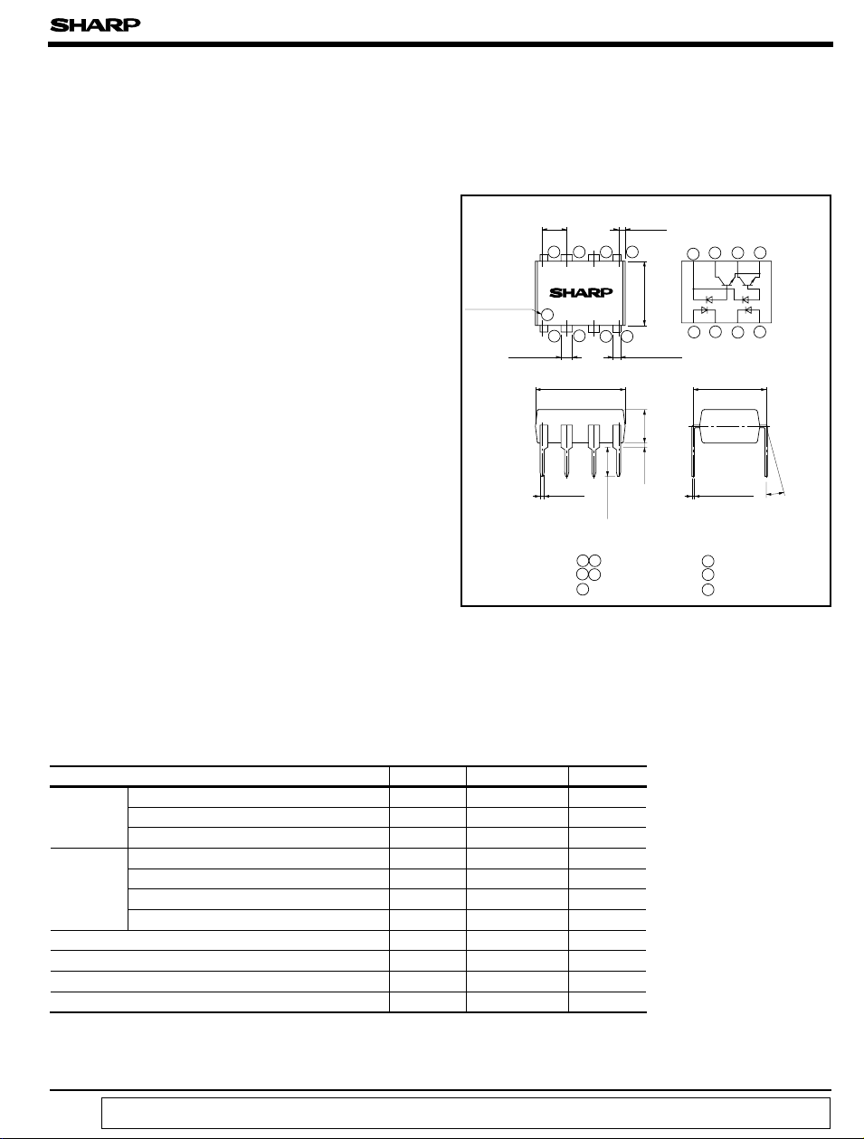
■ Outline Dimensions
2.54
Primary side mark
(
)
Sunken place
± 0.3
1.2
± 0.25
PC9D17
12 34
9.22
± 0.1
0.5
0.8
5678
0.85
± 0.5
± 0.5
3.0
± 0.2
± 0.5
6.5
± 0.3
± 0.5
3.5
TYP.
0.5
(
Internal connection
diagram
1234
± 0.3
7.62
± 0.1
0.26
θ : 0 to 13 ˚
PC9D17
Unit : mm
5678
θ
)
■ Absoulte Maximum Ratings
Parameter
*1
Forward current
Input
Output
*1 Each channel
*2 40 to 60%RH, AC for 1 minute
*3 For 10 seconds
*1
Reverse voltage
*1
Power dissipation
Supply voltage
*1
Output voltage
*1
Output current
*1
Power dissipation
*2
Isolation voltage
Operating temperature
Storage temperature
*3
Soldering temperature
1 4 Anode
2 3 Cathode
5 GND
* “OPIC ” (Optical IC) is a trademark of the SHARP Corporation.
An OPIC consists of a light-detecting element and signal processing circuit integrated onto a single chip.
(
Ta= 25˚C
)
Symbol Rating Unit
I
F
V
R
25 mA
5V
P45mW
V
V
I
P
V
T
T
T
- 0.5 to + 15 V
CC
- 0.5 to + 15 V
O
O
O
iso
- 55 to + 100 ˚C
opr
- 55 to + 125 ˚C
stg
sol
8mA
35 mW
2 500
V
rms
260 ˚C
6 V
7 V
8 V
02
01
CC
“ In the absence of confirmation by device specification sheets, SHARP takes no responsibility for any defects that occur in equipment using any of SHARP's devices, shown in catalogs,
data books, etc. Contact SHARP in order to obtain the latest version of the device specification sheets before using any SHARP's device.”
PC9D17
■ Electro-optical Characteristics
Parameter Symbol Conditions MIN. TYP. MAX. Unit
Forward voltage V
Input
Reverse current I
Terminal capacitance C
)
)
)
I
I
I
OH(1
OH(2
OH(3
Output
High level output current (1
High level output current (2
High level output current (3
Low level output voltage V
Low level supply current I
High level supply current (1
High level supply current (2
)
)
I
CCH(1
I
CCH(2
Current transfer ratio CTR
Isolation resistance R
Floating capacitance C
Transfer
charac-
teristics
“High→Low ”
propagation delay time
“Low→High ”
propagation delay time
Instantaneous common mode rejection
voltage “ High level output ”
Instantaneous common mode rejection
voltage “ Low level output ”
t
t
CM
CM
■ Recommended Operating Conditions
Parameter Symbol MIN. TYP. MAX. Unit
Forward current
Supply voltage V
Operating temperature T
I
F
CC
opr
- - 16 mA
-5-V
0 - 70 ˚C
(
Unless otherwise specified, Ta = 0 to + 70˚C
Ta= 25˚C, IF= 16mA - 1.7 1.95 V
F
Ta= 25˚C, VR=5V - - 10 µA
R
Ta= 25˚C, VF= 0, f= 1MH
t
)
Ta= 25˚C, IF= 0, VCC=VO= 5.5V
)
Ta= 25˚C, IF= 0, VCC=VO= 15V
)
IF= 0, VCC=VO= 15V - - 50 µ A
= 16mA, IO= 2.4mA, VCC= 4.5V
OLIF
= 16mA, VO= open, VCC= 15V
CCLIF
)
Ta = 25˚C, IF= 0, VO= open VCC= 15V
)
IF= 0, VO= open, VCC= 15V - 2 µA
Ta = 25˚C, IF= 16mA, VO= 0.4V, VCC= 4.5V
Ta = 25˚C, DC500V, 40 to 60% RH
ISO
Ta= 25˚C, V= 0, f = 1MH
f
Ta= 25˚C, RL= 1.9kΩ
PHL
PLH
= 16mA, VCC=5V
I
F
Ta= 25˚C, RL= 1.9kΩ
= 16mA, VCC=5V
I
F
Ta= 25˚C, IF= 0, RL= 1.9kΩ
H
VCM= 10Vp-p, VCC=5V
Ta = 25˚C, IF= 16mA, RL= 19kΩ
L
VCM= 10Vp-p, VCC=5V
Z
- 60 250 pF
Z
- 500 nA
-
--1µA
- - 0.4 V
- 400 - µ A
- 0.02 1 µA
19 - - %
5x101010
11
- 0.6 - pF
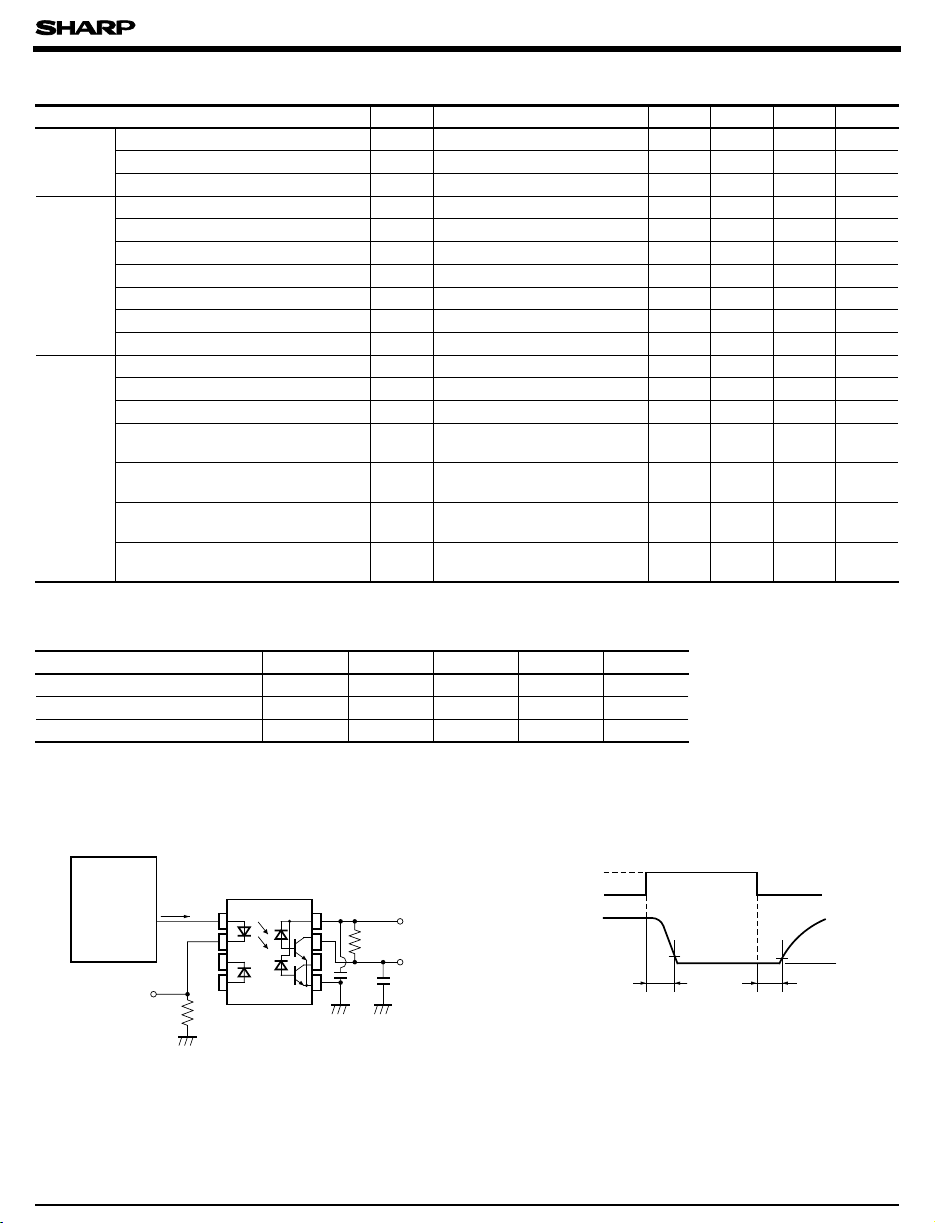
Fig. 1
- 0.3 0.8 µ s
Fig. 1
- 0.3 0.8 µ s
Fig. 2
--V/µs
1 000
Fig. 2
- 1 000
--V/µs
All typical values: at Ta= 25˚C
)
- Ω
Fig. 1 Test Circuit for Propagation Delay Time
Pulse input
Pulse width
10 µ s
I
1/10
100Ω
F
2
3
45
81
7
R
0.01
µ F
L
6
Duty ratio
I
monitor
F
C
V
CC
V
O
= 15pF
L
I
F
0
V
O
1.5V
t
PHL
t
PLH
1.5V
5V
V
OL
 Loading...