Sharp PC929 Datasheet

PC929
(
❈ TÜV
VDE 0884) approved type is also available as an option.
PC929
Shortcircuit Protector Circuit
Built-in Photocoupler Suitable
for Inverter-Driving MOS-FET/IGBT
■
Features
1. Built-in IGBT shortcircuit protector circuit
2. Built-in direct drive circuit for IGBT drive
(Peak output current ... I
3. High speed response (t
4. High isolation voltage (V
O1P, IO2P : MAX. 0.4A)
, t
: MAX. 0.5µs)
PLH
PHL
: 4000V
iso
)
rms
5. Half lead pin pitch (p=1.27 mm) package type
6. Recognized by UL, file NO. E64380
■
Application
1. IGBT control for inverter drive
■
Absolute Maximum Ratings
Parameter
*1
Forward current
Input
Reverse voltage V
Supply voltage V
O1 output current
*4
peak output current
O
1
O2 output current
*4
peak output current
O
2
Output
output voltage
O
1
*2
Power dissipation
Overcurrent detecting voltage
Overcurrent detecting current
Error signal output voltage
Error signal output current
*3
Total power dissipation
*5
Isolation voltage
Operating temperature T
Storage temperature T
Soldering temperature T
*1, 2, 3 Decrease in the ambient temperature range of the Absolute Max. Rating : Shown in Figs 1 and 2.
*4 Pulse width<=0.15µs, Duty ratio=0.01
*5 40 to 60% RH, AC for 1 minute, Ta=25˚C
(Ta=Topr unless otherwise specified)
Symbol
I
I
V
V
V
Rating Unit
I
F
R
CC
I
O1
O1P
I
O2
O2P
O1
P
O
V
C VCC
I
C
FS VCC
I
FS
P
tot
iso
opr
stg
sol
20 mA
6 (Ta=25˚C) V
35 V
0.1 A
0.4 A
0.1 A
0.4 A
35 V
500 mW
30 mA
20 mA
550 mW
4 000 Vrms
-25to +80
-55to +125
260 (for 10 sec)
V
V
˚C
˚C
˚C
■
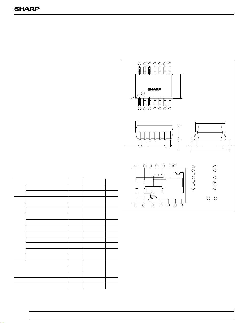
Outline Dimensions
1011121314
89
PC929
Primary
side mark
* "OPIC" (Optical IC) is a trademark of the SHARP Corporation.
An OPIC consists of a light-detecting element and signal processing circuit
integrated onto a single chip.
1234567
9.22
14-
0.6
Internal connection diagram
1234567
Interface
Constant
voltage circuit
12-
1.27
1011121314
Amp.
6.5
0.35 3.5
89
IGBT protector
circuit
0.26
1.0 1.0
1 Cathode
2 Cathode
3 Anode
4NC
5NC
6NC
7NC
Terminals 4 to 7 :
Shortcircuit in element
Operation truth table is shown on the next page.
7.62
10.0
8FS
9C
10
11
12
13
14
(Unit : mm)
GND
O
2
O
1
V
CC
GND
“In the absence of confirmation by device specification sheets, SHARP takes no responsibility for any defects that occur in equipment using any of SHARP's devices, shown in catalogs,
data books, etc. Contact SHARP in order to obtain the latest version of the device specification sheets before using any SHARP's device.”

PC929
Electro-optical Characteristics (1)
■
(Ta=Topr unless otherwise specified)
Parameter Symbol Conditions MIN. TYP. MAX. Unit
Forward voltage
Reverse current I
Input
V
V
Terminal capacitance C
Operating supply voltage
O1 low level output voltage
O
high level output voltage
2
O
low level output voltage
2
Output
O leak current
High level supply current I
Low level supply current I
*7
"Low→High"
threshold input current
V
V
V
V
V
CCH
CCL
I
FLH
Isolation resistance R
"Low→High" propagation delay time
"High→Low" propagation delay time
t
PLH
t
PHL
Rise time t
Response time
Instantaneous common mode rejection
voltage "Output : High level"
Transfer characteristics
Instantaneous common mode rejection
voltage "Output : Low level"
*6 When measuring output and transfer characteristics, connect a bypass capacitor (0.01µ F or more) between V 13 and GND 14 near the device.
*7 I represents forward current when output goes from "Low" to "High".
FLH
*8 FS=OPEN, V =0V
C
Fall time t
CM
CM
Ta= 25˚C, IF= 10mA - 1.6 1.75 V -
F1
Ta= 25˚C, IF= 0.2mA 1.2 1.5 - V -
F2
Ta= 25˚C, VR=5V - - 10 µA-
R
Ta= 25˚C, V= 0, f= 1kHz - 30 250 pF -
t
Ta= - 10 to 60˚C 15 - 30 V
CC
V
= 12V, V
O1L
O2H
O2L
O1L
CC1
I
= 0.1A, IF= 5mA
O1
V
CC=VO1
I
= 5mA
F
VCC=VO1= 24V, IO2= 0.1A, IF= 0mA
Ta= 25˚C, VCC=VO1= 35V, IF= 0mA
Ta= 25˚C, VCC=VO1= 24V, IF= 5mA
VCC=VO1= 24V, IF= 5mA
Ta= 25˚C, VCC=VO1= 24V, IF= 0mA
VCC=VO1= 24V, IF= 0mA
Ta= 25˚C, VCC=VO1= 24V
VCC=VO1= 24V
Ta= 25˚C, DC500V, 40 to60% RH
ISO
Ta= 25˚C, VCC=VO1= 24V
RG=47Ω, CG= 3 000pF, IF= 5mA
r
f
Ta= 25˚C, VCC=VO1= 24V, IF= 5mA
H
L
= 600V(peak), ∆ V
V
CM
Ta= 25˚C, VCC=VO1= 24V, IF= 0mA
= 600V(peak), ∆ V
V
CM
- 15 - 24 V
= - 12V
CC2
= 24V, IO2= - 0.1A
- 0.2 0.4 V
*8
20 22 - V
*8
- 1.2 2.0 V
*8
- - 500 µ A
*8
-1017mA
*8
- - 19 mA
*8
-1118mA
*8
- - 20 mA
*8
0.3 1.5 3.0 mA
*8
0.2 - 5.0 mA
*8
5x10101x10
11
- 0.3 0.5 µs
- 0.3 0.5 µs
- 0.2 0.5 µs
*8
- 0.2 0.5 µs
O2H
O2L
= 2.0V
= 2.0V
CC
- 1 500
*8
1 500
*8
--V/µs
--V/µs
Measuring
circuit
-
(1)
(2)
(3)
(4)
(
)
6
(5)
--Ω
(8)
(
)
7
Truth Table
■
Input
ON
OFF
Output FS OutputC Input/Output
O
2
Low level High level High level
High level Low level Low level
Low level Low level High level
High level Low level High level
For protective operation
 Loading...