

Page 1
PC-1251
SHARP
SERVICE MANUAL
MODEL
CODE:
PC-12
PC
O
OZPC1251
-1250
///
E
51
1.
PRODUCTS
2. SPECIFICA
3. BLOCK DIAGRAM . . .
4. CPU
5. LCD DRI
6. SER VICE PR
7. SCHEMATICS 10
8. PARTS SIGNAL LAYOUT CHART
9. PARTS
*
Differen
Program da
-t:<
CE-125 option
Microcassette tape recorder
thermal
ce
dot pr
INTERNAL BLOCK DIAGRAM AND PIN/SI
VE CIRCUIT
GUIDE AND PARTS LIST
between PC 1 2
ta
area
of the PC-1251 is
:
inter is in
OUTLIN
TIO
N
ECAUTIONS
50 and PC 1251:
is
available as an external me
corporate
d as the output
E
. . . . . . . . . . . . . . . . . . . . . . . .
AND TIMINGS . . . .
. . . . . . . . . . . . . . . . .
larger by 2048
bytes.
devi
. . . . . . . . . .
mory device and 2
ce.
. .
. . . . . . . .
GNAL DESC
. .
. . . .
. .
.
.
. . .
. . .
. .
. .
3
RIPTION
. . . . . . . . . . .
. . . . . . . . . . . . . . . . 9
4-digit
. .
. . . 7
. .
4
11
1
2
SHARP
CORPORATION
Page 2
1
.
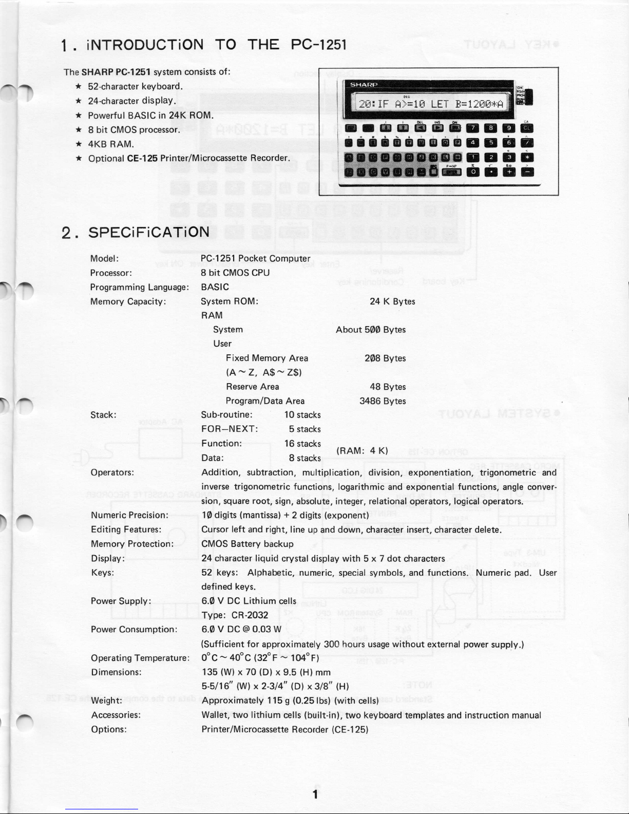
iNTRODUCTiON TO
The
SHARP PC-1251
*
52-character keyboard.
*
24-character
*
Powerful BASIC in 24K ROM.
*
8 bit
CMOS processor.
*
4KB
RAM
*
Optional CE-125
system consists of:
display
.
.
Printer/Microcassette Recorder.
THE
2. SPECiFiCATiON
Model: PC-1251 Pocket Computer
Processor: 8
Programming
Memory Capacity:
Stack
:
Operators:
Numeric Precision:
Editing Features:
Memory
Display:
Keys:
Power Supply:
Power Consumption:
Operating Temperature: 0°C ~ 40°C (32°F ~ 104°F)
Dimensions
Weight:
Accessories
Options
Language: BASIC
Protection
:
:
:
:
bit
CMOS CPU
ROM
RAM
System
User
Fixed Memory Area
(A~ Z,
Reserve Area
Program/Data Area
Sub-routine:
FOR-NEXT
Function:
Data
:
Addition,
inverse
sion, square root, sign, absolute,
10 digits (mantissa) + 2
Cursor
CMOS Battery backup
24 character
52
defined keys.
6.0 V DC
Type: CR-
6.0 V
(Sufficient for
135 (W) x 70 (D) x 9.
5-5/16
Approximately
Wallet, two
Printer/Micr
subtraction,
trigonometric functions, logarithmic and exponential functions, angle conver-
left
and right, line up and
keys: Alphabetic, numeric,
Lithium
2032
DC@0.03
11
(W) x 2-3/411(D)x3/8
ocassette Recorder
PC-1251
:
About
A$~
Z$)
10 stacks
:
liquid
lithium
5
stacks
16 stacks
8 stacks
multiplication,
digits (exponent)
crystal display
cells
W
approximately 300 hours
5 (H) mm
115 g (0.25 lbs) (with cells)
cells
(built-in), two
(RAM: 4 K)
integer, relational operators, logical
down, character insert, character
special
11
(H)
(CE-125)
24 K Bytes System
500 Bytes
208 Bytes
48 Bytes
3486 Bytes
division, exponentiation,
with
5 x 7 dot characters
symbols, and
usage
without
keyboard templates and instruction manual
functions. Numeric pad.
external power
trigonometric
operators
delete
.
supply
and
.
Use
r
. )
Page 3
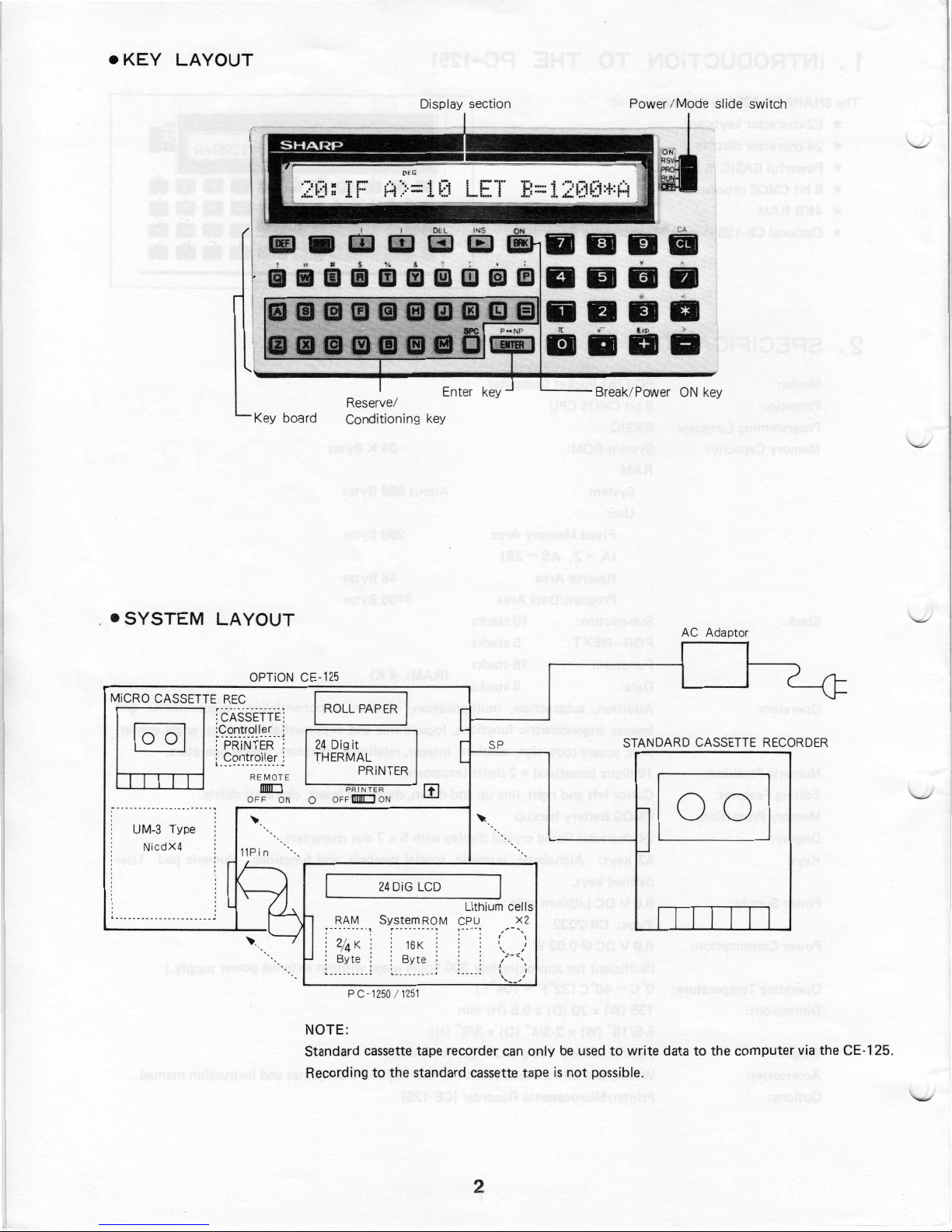
•KEY LAYOUT
Key board
Display
Reserve
/
Conditioning key
section
Power /Mode slide s
witch
.
•SYSTEM LAYOUT
O
PTiON CE-1
MiCRO C
ASS
ETTE REC
:cAssETT-E:
~ci~-~~i1:~--1
: Co
ntrol
ler
1
----
---
- - -----
REMOT
DIDO
OFF ON
UM-3 Type
NicdX4
11Pin
25
I
:
..
E
ROLL PAP
24 Dig it
THERMAL
OFF
0
: 2/4 K
: By
..
R
AM
PRINTER
PRiNTER
llilI[J
:
te
:
_
P C-1250I
ER
I
ON
24 DiG L
System
: 16K
: Byte
1251
CD
ROM CPU
:
:
NOTE:
Standard cassette tape recorder can
Recording
to
the standard cassette tape
SP
Lithium cel
/
s:
<,
I
..
__
'
X2
,,..
ls
'
only
AC
Adaptor
STANDARD C
be
used
to write
is
not
possible
.
data
ASS
ETTE RECORDE
to
the computer via the CE-
R
125
.
2
Page 4
3.
PC-1250 / PC-1251
SYSTEM
BLOCK DiAGRAM
~-G ...
T ..
. . . ....
~~
~
V
GG
,KEY M
(
51 KE
B
UZZ
. .
....
N_D
+
z~
-
V
CJ
~
-
--.
.....--1A1
Slide Switch
ER
.
.L
.r,
dT
....
....
(OPTiON) CE-125
V
GG
3'
!
__ vcc v
oc
GG
SC61860
SC618
TEST
RES
ET
- KON
I
r+ IA
s
I
B1
ATR
iX
Y+ ON KEY
c:::i
Y.~:0
Vots
C.P.U.
o
60 A02LD
-IB4 Xo
)
IY
1
Vs VM
A02
r
Xi
• . .
VA
H
D
R/W~---
¢AL>-------+.-...._--+l--~------t--
01-0s •
AO 1-3
B01-1~=
I
IBs IB1 FOu
IB5 IB
Se
SeiZ Din Dou
L':::::
3
11 V\cK BUSY
.
1')..
.
4
~
' ~
~
VGG-
A
IS
...__ _ __._..,DiS
LCD 24Dig +
VA
Vs
Vrns
SC43536LD
-
HA
C
BOs
SC
E
PAL R/
J
4 3 5
or
I
?symbols
36
W
01-
s
--+--+-_._--1-1---------,,.........----~
-
---~
DATA BUS
l
~=====l==::::;::;:=:#:======t===n=fj=~=
B03,F01
====
t
====
-3
=l==;:;:il:=:#:======t==n::::fl=fj=~
=:!==l:l:::li==J~====;==r=t==fAF~:::>~
F0
5
ROM
16KBYte
LH532916
.
F03 I
'
~
C
E
R/W
CE RAM
2KBy
HM61 1
or
CTC5517)
RAM 2Kbyte
PC1251 Only
Ao-
10.
01-8
te
6
I
)
ADDRESS BUS
CHiP E
NABL
E
'
MiCRO CASS
MiCRO CASSETTE
tape recorde
CiRCUi
M
-13H
ETTE
T
remot
e
THER
r
PCU
SC6858
MAL PRi
MTP 201-24BA
NTE
R
3
Page 5
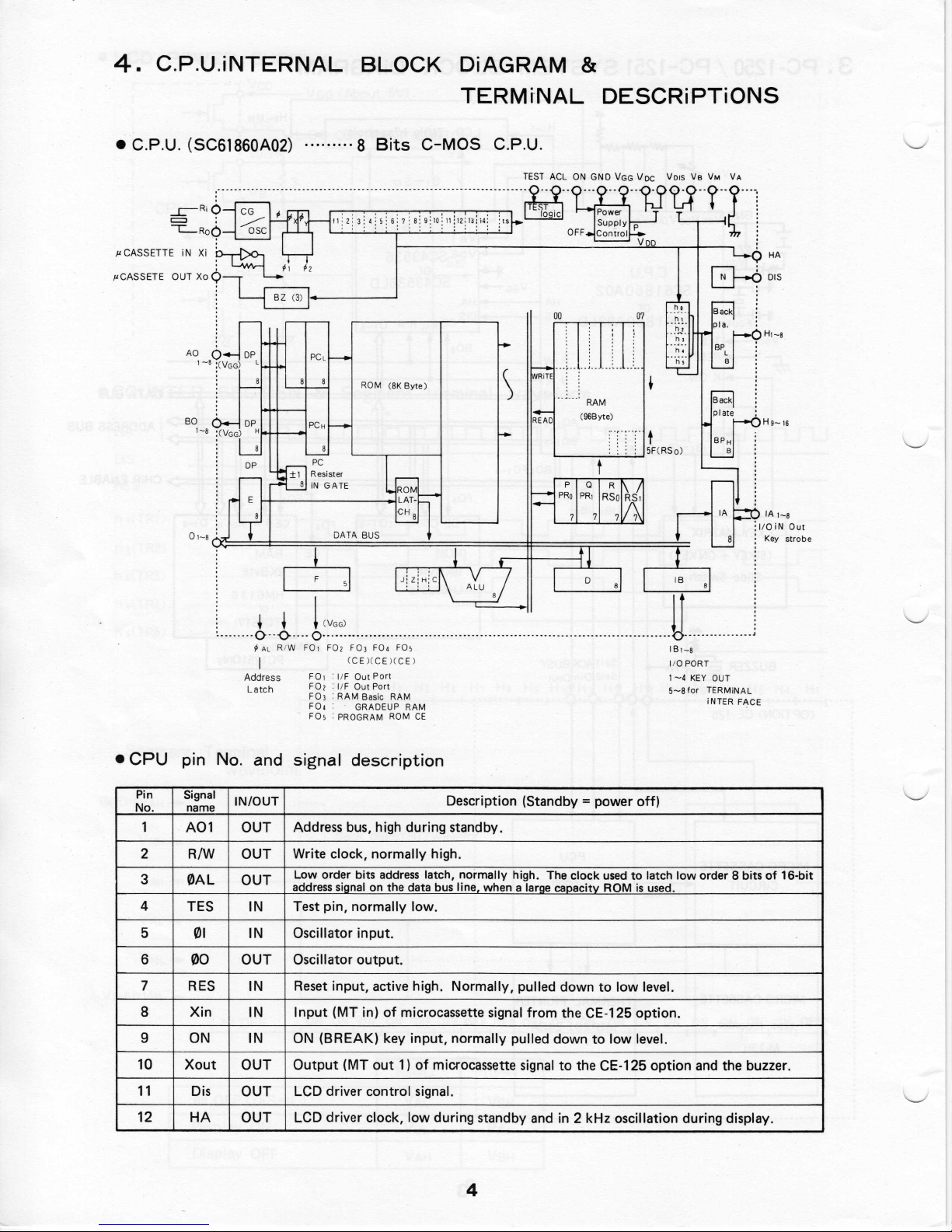
4. C.P.U.iNTERNAL
BLOCK DiAGRAM
TERMiNAL DESCRiPTiONS
&
• C.P.U.
(SC61860A02) ········· 8 Bits C-MOS C.P.U.
ROM (
BK Byte)
I
,
1
DO
07
Hg-15
I
B
•
!
•CPU pin No.
Pin Signal
No.
10
11
12
name
1
A01 OUT
2
3
4
5
6
7
8
R/W OUT
0AL
TES
01
00
RES
Xin
9 ON IN
Xout
Dis
HA
xLh:~.
¢
AL
R/W F01 F01 F03 F04 FO;
Addre
ss
Latch
and si
I
N/OUT
Address
Write clock, normally
OUT
Low order bits address latch, normally hi
address signal on the data bus line
Test pin, normally
IN
Oscillator input
IN
.
CCE)(CEJCCE)
F01 · 11F
Out
Por
F02 : !IF
FOi .
RAM
FO,
F
O; . PROGRAM ROM CE
gnal description
t
Out Port
Basic
RAM
GRAOEUP
RAM
bus, high during standby
low
.
s
Description (Standby = power
.
high
.
gh. The clock used
when a larae caoacltv ROM is
.
to
off)
latch
used.
U
181
-B
110 PORT
1-4
KEY
5-8 for
low
order 8 bits
j
OUT
TERMINAL
INTER FACE
OUT Oscillator output.
Reset input, active high.
IN
IN Input (MT in)
of
microcassette signal from the CE-125 option.
Normally, pulled down to low level.
ON (BREAK) key input, normally pulled down to low level.
OUT Output (MT out
OUT
LCD dri
ver
1)
of mi
crocassette signal to the CE-125 option and the buzzer.
control signal.
OUT LCD driver clock, low during standby and in 2 kHz oscillation during display.
of
16-bit
4
Page 6
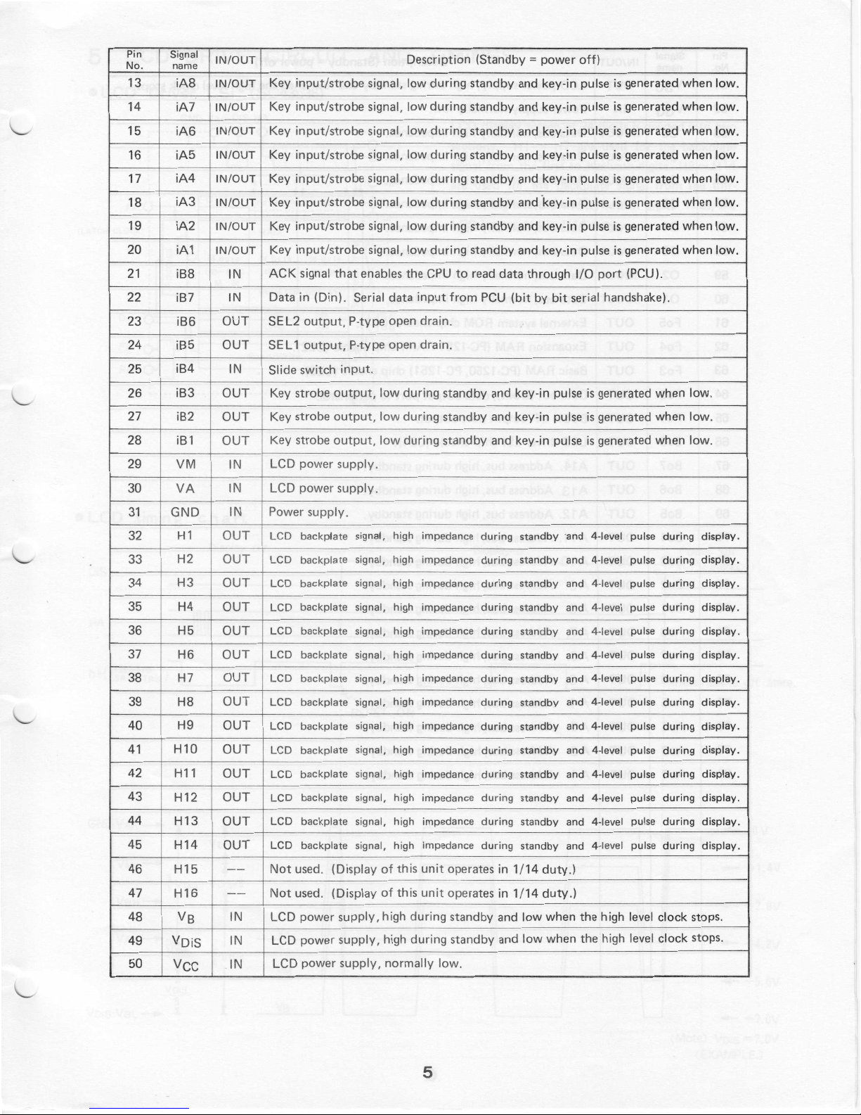
Pin
No
1
3
14
.
Si
gna
l
name
i
A8
i
A7 IN
IN/OUT
IN/OUT
/OU
T
Key input/strobe signal, l
Key
input/strobe signal, l
Description (
Standby = power
ow during standby and key-in
ow during st
andby and key-in pulse
off
)
pulse
is
genera
ted when
is
generated when
low
low
.
.
15
16 iA5
17
18
IN/
i
A6
IN/OUT
IN/OUT Key input
i
A4
i
A3
IN/OUT
OUT
Key input/strobe si
Key input
Key input/strobe
/strobe
/strobe si
gnal, low during standby and
signal , l
ow during
gnal
, l
ow duri
signal, low duri
19 iA2 IN/OUT Key input/strobe signal, low
20 iA1
21
22
23 iB6
24
25
26 iB3
27
28
29 VM IN
30
31
GND IN
32
33 H2
3
4 H3 OUT
35
36
37
38 H7 OUT
39
40
41
42
43
44
45
46 H15
47
48
49
VD i
50
IN/OUT Key input/strobe sig
iB8 IN
i
B7 IN
OUT
i
B5 OUT
iB4
OU
iB
2
OUT
iB
1
OUT
ACK
Data in
SEL2 output, P-type open drain.
S
EL 1 output, P-type open
I
N
S
lide switch input.
Key strobe output,
T
Key strobe
Key strobe
LCD power supply
L
VA
IN
CD
Powe
H1
OUT
O
H4
H
OUT
5
OUT
H6 OUT
H8 OUT
H9
H10
H 11
H12
H13
H14
OU
OU
O
OUT
OU
OU
--
H16
Vs
Vee
-
s
LC
L
UT
UT
CD
LCD
LCD
LCD
LCD
LCD
LCD
T
LCD
T
LC
LC
LCD
T
LCD
T
LCD
Not used. (D
-
Not used. (Display
L
I
N
IN
IN
CD power
LCD pow
LCD power supply,
D
D
D
nal, low duri
signal
that en
ables the CPU
(Din). Ser
ial data input fr
low
output, low
outpu
t,
low during standby and
during
during standb
.
powe
r supply
.
r supply.
back
plate
bac
kplate sign
b
ackp
late
bac
kplate
b
ackplate si
backpla
te signal,
backplate signal,
backplate
backplate
backplate
backplate signal
backplate
backplate signal, high impedance
backplate
isplay
signal
al,
signal
signal,
gnal
signal,
signal,
signal
signal
signal
high
,
hi
high
,
high
high
,
high
high
high
high
high
,
hi
,
high
,
high
,
of this
gh
gh
of this unit opera
supply, high during
er supply, high du
normally
key-in pulse
standby and key
ng
standby and key-in pulse
ng standby and -key-in pulse is
during standby and
ng
standby and key-in pulse
to re
ad
data through
om PCU
drain
.
standby and
key-in
(bit
by
bit serial handshake).
key-in pulse
y and key-in pulse
key-in pulse
i
mpedance
i
mpedance
impedance
impedance
i
mpedan
i
mpedance
imp
edance during standby and 4-l
impedance
impedanc
impedance
impedanc
impedanc
impedance du
unit op
ring stan
duri
ng standby 'and 4-
during
standby
during standby and
during standby
ce during
e
e
e
erat
tes in 1/
standby a
standby and
duri
ng
sta
duri
ng
standby
during standby and
during
standby and 4-l
during standby
during
stand
during
sta
ring
standby
es in 1/14
14
nd low when the high level clock
dby and low when the
low
.
ndby
by and 4-level pulse
ndby and 4-le
duty.
duty.)
is generate
-in pulse
is
ge nerated when
is
generat
genera
pulse
is
ge n
era
is
generated w
1/0 port
(
PCU).
is
gen
erated
is generated when
is generated when
level pulse
and 4-level
and 4-level
and 4-l
and 4-l
and 4-l
and 4-level
pulse dur
4-level pulse during display
puls
e
4-level pulse
evel pulse
evel pulse
evel pulse du
4-level pulse du
evel pulse
evel pulse
vel pulse
pulse during
)
high level cloc
d when low
low
ed wh
en low.
ted when low.
ted when low
hen low.
when
low
.
low
.
low
.
during display
ing
dis
play
during dis
during display
during display
during di
duri
during
during
during displa
ring
ring
ng
display.
display
dis
dis
display
display.
stops
play
spla
play
play.
.
k stops.
.
.
.
.
.
.
.
.
.
y.
.
.
.
y.
5
Page 7

Pin Signal
No
51
52
53
54
55
56
57
58
59
name
.
Voe
VGG
08
07
06
05
04
03
02
60 01
61
62
63
Fo5 OUT
Fo4 OUT
Fo3 OUT
IN/OUT
OUT
IN
IN/OUT
IN/OUT
IN/OUT
IN/OUT
IN/OUT
IN/OUT
IN/OUT
IN/OUT
Description (Standby = power
LCD power supply, high during st
andby and low when the high
Power supply normally low.
Data
bus, normally high
impedance
.
Data bus, normally high impedance.
Data bus, normally high
Data bus, normally high
impedance
impedance
.
.
Data bus, normally high impedance.
Data
bus, normally high
Data bus, normally hi
Data bus, normally high
impedance
gh
impedance.
impedance
.
.
External system ROM chip enable (CE1).
Expansion RAM
Basic RAM
(PC· 1251 RAM) chip enable
(PC-1250, PC-125
1)
chip enable (CE3).
(CE2)
off)
level
clock
stops
.
.
64
Fo2 OUT Data out
65 Fo1 OUT
66
67
Bo8 OUT
Bo7 OUT
68 Bo6 OUT
69 Bo5 OUT
70 Bo4 OUT
71
72
73
Bo3 OUT
Bo2 OUT
Bo1 OUT AS.
74 Ao8 OUT
75 Ao7 OUT
76 Ao6 OUT
77 Ao5 OUT
78 Ao4 OUT
79 Ao3 OUT
80
Ao2 OUT
(Dout), data
BUSH l/F output
output port
port output.
LCD driver LSI chip enable (CE4).
A 14.
Address bus, hi
A13. Address
A 12.
Address bus, hi
A 11.
Address
A 10.
Address bus, high
Address
A9.
Address
Address
A7
.
Address bus, high
A6
.
Address
A5
.
Address bus, high
A4
.
Address
A3
.
Address
A2
.
Address bus, high during standby.
A
1.
gh
during st
bus, high
duri
ng
gh
during standby
standby
bus, high during standby.
during
standby
bus, high
bus, high
bus, high during
bus, high
during
duri
ng
during
during
during
standby
standby.
standby
standby.
standby.
standby
bus, high during standby.
bus, high dur
ing standby.
to per
andby
ipheral.
.
.
.
.
.
.
.
6
Page 8

5.
LCD
DRiVE
CiRCUiT
AND
TiMiNGS
•LCD
Driver LSi
GND
1·-
- --- -9---?-
:
¢AL
~-
-
-
--·-
- - - -
V
GG
~-
l--
--
-
. .
(SC4353
DIS HA
6)
~
~
----'
--~
64 by
te
) (00-3F
)
.
-
-
-- --
64 byte
DISPLAY
S63
------------
M M
(40-7F
(
RAM FOR
-+--(-S6~2)---i-~S6~1_____,
(S63
Read/Write
· -
--·---
-
-
LCD display screen of 24 digits
Vtns
V
A
.
~
:
Qj ):
0
:
~
.
)
c
•
<l)
•
E
:
)
Ol
<l)
~
- -
-·
80P
in
sections,
signal from the first
are used for the
teenth
L
CD
H 1 - H 7
digit
to the twenty-fourth
is
operated
in
are used for the backplate
to
twelveth digits. H8 - H
backplate si
1/14
duty.
is
divided into two
gnal from
digit.
Thus, the
the
thir
14
-
• LCD timing ch a rt
Disp
lay out
bis
HA
GND-VAH
VMH-
VBH
-
f
V
DiS
l
/
I
3
-
5\
DiS
Vot;s/5
*
VAL
-
t
vo.
s
~v .
5
DIS
s
1
VM
VDis·VsL
-5-
L
- t
voi
- T
Power ott
(CPU standby)
Retains the oft . atate
~
~
'---
(Mote
)
vois
(EX
AMPLE
- av
- -1.4V
- -2.BV
-
-4.2
V
..,_ -5.6V
- -7.0V
=7.0V
.)
.
Lt:
RES
ET ON
Display
on
-
5
-
·
-
VA
VM
VB
7
Page 9

•LCD
r------
POWER
-
--l
SUPPLY
Vee
V
oe
L
VDiS
VGG (About
CD CONTRAST
6V)
CONTOL
S
1
CP
U
•COUNTER
H
A
DiS
RE
S
h 1CTR1)
h
2CTR2) -- - ----
h 3(TR3)
h 4(TR4
)
h
5(TR5)
--l
--l
SECTiSN
------------------
- -------
Vs
LC
V
M
I
1
VA
&
- - ---
--
- -
- -
---
- ---
----.
D
DRiVER
Segment
(
s
62
terminal
waveform
LJ
Segme
GND=
VAH
V
vrns=vsr
nt
Termi
-
MH -.-------------- -
_.
all OFF (DiS=L)
D
isplay
Display OFF
nal
w
aveform
- - - - -----
-
a
l l
OFF
ON
B
ack plate (H1) wavefor
ON ON ON
ON OFF OFF OFF OFF OFF
h5=0
VAL
V
BL
VAH
8
h5=1
V
BH
VA
VBH
OFF ON ON
H
ON ON ON ON
ON ON OFF
Page 10

6. SERViCE PRECAUTiONS
1.
Since it
you use
shooting purposes
is
difficult to troubleshoot the
the
service tool
chassis (LCHSS1134CCZZ) which
only. When
unit
main PWB because of chassis
is
is
repaired, replace with original chassis.
mounted
smaller in size. Install this chassis
on
top
of it, it
is
suggested
for trouble-
that
2. When
3. If
4. Consumption
5. Checking display
the
memory module PWB
could be installed slightly
to the
play in
l
ead
to
again and press
resuming
the
lithum
with good electrical
flickering display or
result.
o
Supply voltage: 5.8 V
o
Consumption
400
ON key).
45
µA
OFF key).
Be sure
before
meter
.
the
improper
operation.
battery
Be
sure
current
µA
max. when ON (after pushing of
max. when OFF (a
to
the
measurement
is
out of
alignment due
screw
holes. Since this could
operation, replace
the
ALL RESET switch befor
is
not
installed properly and
contact
damage
the battery
measurement
current
press
the
quality and adjusting
problems such as
to other
is
properly installed.
:
fter pushing of
ALL RESET swi
.
replaced it
the
PWB
parts could
the
the
tch
potentio
-
~'"''
e
:
Not
e
:
No
~
'
to
blur
at 30°.
irregular contrast
at 10°.
9
Page 11

7
.
LF-
CiRCU
81256E
s
s1 s1s s l s l s sis slsls
3 4 5 u 12113114 15
iT
(
24
I
l
Di AGRAM
Dig 5X7
DOT
islslslsl
21
?.212312412513
MATR
iX
s sis
1
~1331343514
s
1
2j43~f45146
l s l s l
Bsvmbols )
s ] s
sls !s] s s
7\4
814
9150
sl
sls l s
51
52l53154J~56l57ffi
l sl
s s l s
js l s
sJslsls
1142141 35j
s l s
ls
l
s ] s s sis
34J33l3~12 2412
sis s sis
3221211514
I
I
I
l
I
I
I
"
1
I
<!
12
II
.......
1 I
,\
b
s
SISIH ",l"I"
2 I 14 13
3
00
I
s s
sis
5 4
13
12111
-
Addre
ss Bus
Data Bus
--l
•
Segment
ti--
t
-
----
-
,---
:::::::
,.--
,,.- 0
,.--
-
---F
--1
_~~~
_.';!
.'!_
~
c
~
1
~
(
:£<
F
-
'"F
-
l
+IGND
(
-) VGG
r---
--tt-----
~
----------- .....
------------ri
I
I
I
I
I
I
j
I
I
I
'1
11'---
'------f
- ~
-
.E!_
1- ~ ~
I'--
r---
~
r--- Al
.__
T
I I
I
•
s
2K By
HM611
or
T
C5517
RA
6
te
M
A4
:T
5 20 ~{;
- F04 - F03 r---
"'AO
......
..i
Oi
~
10
~
G
ND 12
1-'i
: I
I I
~
-
-~C_!_2~1_9~
'=._Y
24.YQ.Q_
t--
A9
l----+--~1--+--v
E
l.
..IT_
0
0
:2L
1
5~
o
s
13 04
..........
-+-it--
I
I
I
I
I
I
1
1
I
ii
j
-..
---------
.....
-------
---4
...+.-t----+--it---..-------
11
- ~ -
·--
g_
I
~
-~-~
~
-----
----- ~~
--------~
..___
~
_
l
2K Byte
~
5
HM6116 1<.b,_CEE"t-.,.:.:~+--
~
~ 10
TC5517
~
..§.!!_Q
12
rrt, ..-J- - ........... --.- ...........................
or
24
...Y.QQ.
~ r++ur,
~
t----+--+-il-
~ ~
E'!!.
-
20
ffo-
RAM
-
0
0
Q?
i----+---1111
15~
'-----+------"•
~
i----+---1111 .__
1
3
..Q..1._
I---+-
-
......
-
1'---1
~
~
~
r---
~ 35
~
~
~
~
~
,____
..!2.
16K
40
L
44
I
101
~ 1~1~
~
J
-
---4t------+--
25
Byte
ROM
H532916
5
~
6 ~ ~ ~
10
-
.ss:
20 ....!..2_
~
~
~
-
15~
-
~
Page 12

(jJL) x3
VGG
V
DC
V
B
VA
SC61860A02
( SC6 I 860A02LD)
VGG
C
PU
3.3JJF
LI 220
Lithium cell
r
CR2032x2
GN
D
116K Byte
ROM
_H532916
Rese
t SW IOO
LSi
Terminal (Option
G
ND
VGG
'-+-+-+-+-<>--+-~~
1
FO I
'---+-+-+-t-+-+--~~l F02
Xout
Xin
IB
IB7
IB6 SEL2
I
B5
B
PF.12
signal name
Side
M
Tou
t2
G
ND
V
GG
Busy
0 in
MT in
MT
outl
Dout
ACK
SELi
L..------ _J
)
OPTION INTERFACE
11PIN CONNECTOR
10
Page 13

8. PARTS
&
SiGNAL POSiTiON
11
Page 14

Page 15

12
Page 16

13
Page 17

13
Page 18

P
ART
R
ANK
B
c
B
c
B B
c
c
c
c
c
c
B
B
B
c
c
c
B DiO
B
B
B
c
c
c
c
c
c
E
E
c
B
B
S
11
PiN CONNECTOR (F
RESET
F.P.C
TERMiNAL FOR
UZZ
ER
C
APACiTOR (CHiP)
CAPACiTOR (CHiP) 1
C
APACiTOR (C
CAPACiTOR 0. 1µF 12V
C
APACi
TOR 1 µF 6.3V
C
APACiTOR
PARTS NEME
SWiTCH
HiP) 0.01
3
.3µF 1 O
X'tal
VARi
ABLE
TRAN
RE
SiS
CAPACiTOR
C
APACiTO
DE 1 S1
Z
ENER Di
LSi
LSi (OR VHiSC6186
RESiSTOR (CHiP) 1 OOKD
RESiSTOR (CHiP) 1 MD
RESiSTOR (CHiP) 22!1
RE
SiS
RESiSTOR (CHiP) 56K!1
L.C.D
ME
MORY MO
MEMORY MOD
SPRi
NG
L
si
L
si
RESiSTOR
SiS
TOR (CHiP) 2SC2
TOR 20KD±5%
lOOPF 50V
0.033
R
588L2
ODE
RD6.2
SC43536
TOR (CHiP) 4.7K!1
.
DULE PWB
ULE PWB UN
)
TERMiNAL
BATTER
Y
0.1
µF
OOPE
µF
V
µF 25
E8
0A01
)
U NiT FOR PC1250
(L5,L6)
81
2
V
iT FOR PC1251
NE
No.
43 QCNW-1236CCZZ
-
~
66
-
'---
~
PARTS CODE
QCNCW1306CC1B
QCNTM1051CCZZ
QTANZ1289CCZZ
RALMB1030CCZZ
RC-CZ1021CCN1
RC-CZ1035CCN1
RC-CZ1037CCN1
RC-CZlOOOQCZZ
RC-SZ1007CCZZ
RC-SZ1021CCZZ
RCRSZ1046CCZZ
RVR-Z2400QCZZ
RH-i
X1012CCNl
RR-KZ1050CCN1
VCKYPU1HB101K
VCTYPU1EX333M
VHDDS1588L2
VHERD 6. 2E8 /-1
VHiSC43536
VH i SC6 l 860A02
VRS-TP2BD104J
VRS-TP2BD105J
VRS-TP2BD220J
VRS-TP2BD472J
VRS-TP2BD563J
VVLLF8126E
DUNTK6915CCZZ
DUNTK6917CCZZ
MSPRC1207CCZZ
VHiLH532916
VHiTC5517AF
/-
1
/-
-
PRiC
RANK
AK
AB
A
C
A
B
AD
AB
A
A
AB
AF
AC
A
A
A
AA
AA
AB
-
1
A
D
AC
A
X
BE
AA
AA
AA
AA
A
A
l
A
Y
AB
l
-
AZ
1
BE
W
E
MARK
N
B
B
N
E
N
F
C
N
N
N
N
N
-g'D
OvtvTk
- 'q
1
7cc
~
R<t.
15
.MJZM
Ao 1)
p
(.
l l-
c; 0 ..4
Page 19

•PARTS GUDE
16
Page 20

SHARP CORPORATION
Industrial Instruments Group
Reliability & Quality Control
Yamatokoriyama, Nara
December. 1982
639-11,
Printed
Department
Japan
in
Japan
(Y)
 Loading...