

Sharp MZ-8BI03,MZ-8BI04 Service Manual
)
SHARP
SERVICE
MANUAL
PDSMX81013-MZ
ft'
In
Ill.
In
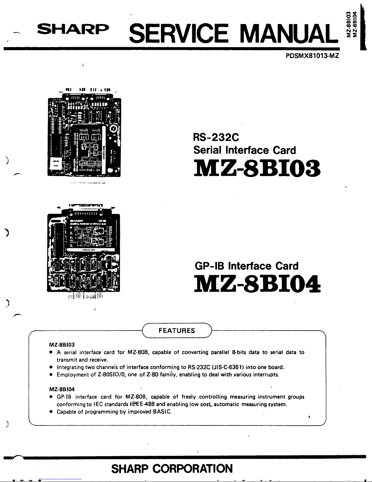
RS-232C
Serial Interface Card
MZ-SBI03
, "
•.•• " ...... , .... ~ ..
~I
.......
GP-IB Interface Card
MZ-SBI04
FEATURES
MZ·8BI03
•
A
serial
interface card
for
MZ·80B. capable
of
converting parallel 8-bits data
to
serial data
to
transmit
and
receive.
• Integrating
two
channeis
of
interface conforming
to
RS·232C (JIS·C·6361)
into
one board.
• Employment
of
Z·80SI0/0.
one
of
Z·80 famiiy, enabling
to
deal
with
various interrupts.
MZ·8BI04
• GP·IB
interface card
for
MZ·80B, capable
of
freely controlling measuring instrument groups
conforming
to I EC
standards
~
~E-488
and enabling
low
cost, automatic measuring system.
•
Capable
of
programming
by
improved BASIC .
~~
..................................................................
..
SHARP
CORPORATION
~-------Contents--------
MZ·8BI03
Specifications.................................................
1
General information
.................................•...•.......
2
Description
of
circuit
...............................•............
3
Troubleshooting. . . . . . . . . . . . . . . . . . . . . . . . . . . . . . . .
• . . . . . . . . . . • . .
..
8
Test program
..................................................
10
PWB
and
circuit
diagram
..........................................
15
MZ-BBI04 Specifications
.................................................
18
Description
of
circuit
................................•....•••...•
19
Troubleshooting
..............................•.....•........•..
23
PWB
and
circuit
diagram
........................•..•.•....•.......
27
Packing method
........................
'
................•.•....•...••....
30
Replacement parts list
...........................................•.....••..
31
MZ:..8BI03:.SPECIFICATIONS
,~,~,
Item
Communication me'thod
Standard
Control
LSI
Number
of
channels
20mA current loop
Baud
rate
Number
of
baud
rates
Character length
Parity
bit
Stop
bit
Mode
Interrupt
Port
address
Operating temperature
Storage temperature
Specifications
Asynchronous
In compliance
with
EIA
RS·232C
Z·80SIO/0
2 (Channel A and Channel B)
Changeover
is
allowed
for
orie channel (Channel
B)
Can
be
set
independently
for
the
two
channels (Manual setting using switch)
10(75,110,
150,300,600,
1200,
1800,2400,4800,
9600 baud)
5,
6, 7
or
8 bits (Selection
by
software)
Odd, none
or
even
.
1,
1
Y.
or
2
Either terminal mode
or
modem mode
can
be
selected
for
ellch channel
(through the
use
of
jumper chip).
Z·80 vector
interrupt
can
be
used.
,
..
Manual setting
with
switch
O°C-
50°C
-25°C-
80°C
(Note) The above·mentioned specifications may be changed ir, the future
for
improvement
of
the product.
<.
f
" '
r
"
)
)
• Introduction
Ther~
are
two
methods
of
data communication between
computer
and external equipment: S-bit parallel and
bit
serial.
The serial interface card MZ-SBI03 (hereinafter referred
to
as "interface
~ard")
permits data communication by the
bit
serial method. This interface card
is
manufactured in accordance with EIA RS-232C (the Electronic Industries
Association RS-232t::), and used for data communication with
other
equipment having interface based
on
RS-232C.
•
Functions
of
this
interface
card
The interface card has
the
following functions.
1.
One card has
two
channels, each
of
which
is
capable
of
transmitting/receiving data independently.
2.
One
of
the
ten baud rates can be selected by operating
the
switch
on
the
card. Baud rates can be set independently
for
the
two
channels.
3.
Output
connector signals
to
external equipment can be
in
either terminal mode
or
modem mode through the
operation
of
the
jumper chip.
4. This interface card can be used as
20mA current loop for one channel.
•
Applications
Equipped with
the
above-mentioned functions,
the
interface card has a variety
of
applications. Some applications
of
this very versatile serial interface card are shown below.
1.
Data communication between computers on telephone line via acoustic couplers
2. Printer
3.
Plotter
4. Digitizer
5.
Color display
6.
Card reader
7. Magnetic tape equipment
.
\
•
2
)
.~
)
•
n
3::
~
N
n
c
~
;+
I
D
....
~
~
TxDB
./
Current
~
0
ex»
RS-232CI
Loop
~
&.
e
ca
RxDB
Drive
~
Current Loop
Cl)
Select
3
0
DTRB
CA)
Co"",,'
••
' q
-)
Mode
Channel B
Select
Connector
C
(J-2)
v
m
RS-232C
~
en
~
Drive
/
0
Rml
I
..
CTSB
:D
..
-
DCDB
I (J-1)
"
....
-
H~~'Cb
0
furt
H
Z
Add'~~
Address -
Bus
Select
TxDA
.
',"~
.
:-
W
0
Circuit
..
RxDA
"
RS-232C
Mode
Channel A
• '.""',.1-,.
RTSA
Drive
Select
Connector
0
-
CTSA
DTRA I
(J-3)
I:D
0
DCDA
c:
-
+5V~
['m
~
Power
Chlnnel A
.~;~";
Supply
BR2
Baud Rate Setting
(SW-21
Blud
Rate
t',
Circuit
v..;..#
-12V
Oscillltion
f~";
Circuit
Channel B
.:\
BR1
14
Baud Rate Setting
(SW-31
.
'C
r·._
-
-
-
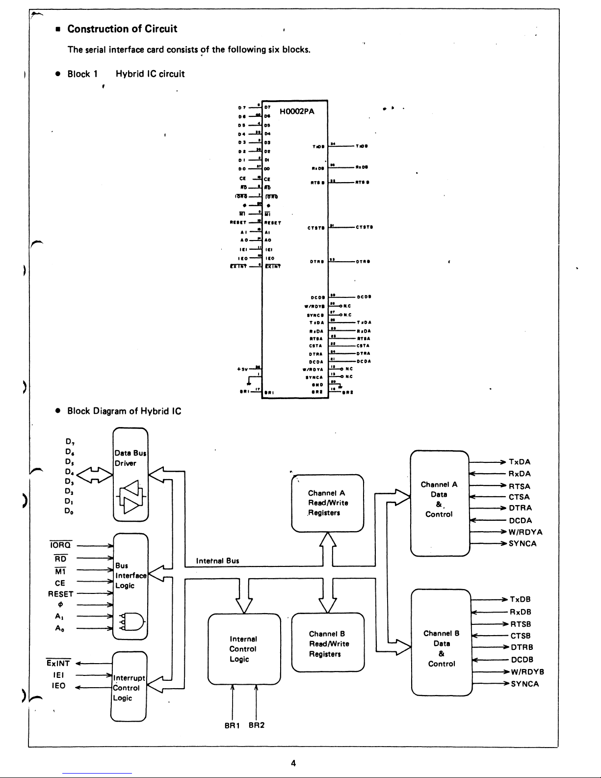
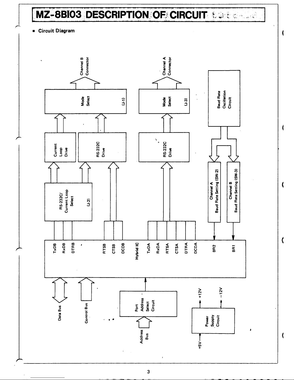
• Construction
of
Circuit
The
serial
interface
card
consists
?f
the following six blocks.
• Block
1
Hybrid
IC
circuit
D'
D'
HOOO2PA
01
D.
D'
D'
.
..,.
01
D'
00
IhO'
Cl
It"
•
1111
.1JII1i
rntI
• •
In
1t11'T
CTITI
A'
r
AD
'1'
'1'
'10
.10
DTItI
..
rnn
• RT1il
DCDI
••
.,.0
....
N.C
IY"CI
..
N.C
,.DA
H
••
0&
..
It'l.
CITA
DT
••
DCD"
+.v
.,,,oYA
'''''CA
)
IND
U.
U.
•
••
•
Block Diagram
of
Hybrid IC
0,
D.
Data BUI
0,
Driver
<:>
~
..
0
Channel A
Read/Writa
.Reglsters
D.
0,
)
O
2
D.
Do
lr
Bus
fG:
Intetnal Bus
Interface
Logic
U
U
D
Channel B
Internal
Read/Write
Control
Registers
Logic
IORO
RD
Ml
CE
RESET
~
A.
AD
ExlNT
~
I!"terrupt
Control
"-r--
Logic
IEI
IEO
)
I
BRl
BR2
4
•
•
.
..,
.
....
"TI'
C'I'I
DT.'
DCOI
'IDA
'hO&
ItTI"
CSTA
0'"''
DCO'
~
~
Channel A
Data
&
Control
Channel B
Data
&
Control
TxDA
RxDA
RTSA
CTSA
DTRA
DCDA
W/RDYA
SYNCA
TxDB
RxDB
RTSB
CTSB
DTRB
DCDB
W/RDYB
SYNCA
• Block 2
Port
Address
Select Circuit
147
A.
A'
144
145
142
SW-I
LS2&'h2
le4
5.51\"6
RA I
+5V
..
I.
I
e4
I
e4
le4
le5
le
5
CE
.SV
• Block 3
Baud
Rate
Oscillation
and
Setting Circuit
R~OK
10
REiE'f
.SV'-~""'+'"
B
II
I
.••
JI
....
+'V
___
---='.::j4
..
IC
I
MCI4411
ICl
RH·iX0297PAZZ
(MC144ll)
PIN
ASSIGNMENT
(Top View)
24
2
23
3
22
4
21
20
6
19
18
8
17
9
16
10
15
11
14
12
13
Rite
Sllect A 23
RI.I
Select 8
22
Cryltlljn 21
•
"
Cryltl1o..n:
20
R.Mt
10
sw-z
IBI
5
IC3,4
RH·iX0190PAZZ
(SN74LS266N)
PIN
ASSIGNMENT
(Top View)
1A2
BLOCK DIAGRAM
I
.1
Divide ...
Rill
Select
LotiC
(
(
c
c
Fl
11
f2
2
F3
16
F4
3
F5
15
f6
4
F7
5
F8
7
F9
e
Fl0
8
Fll
14
f12
13
FI3
C
11
F14
18 F16
19
F16
)
)
)
)
)
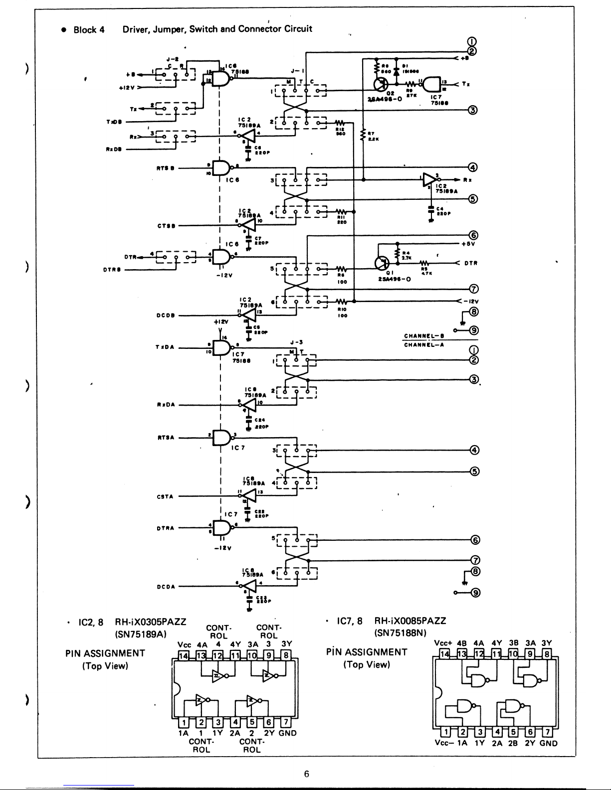
• Block 4
,
Driver, Jumper, Switch and Connector Circuit
./-1
L..
__
~
...
~.sf
1
+IIV"
TIDI
____
-.J
Ic2
, 751
..
"
It.
01
1
,....---...,
'<1
It.~
t
_000
~-iI--+-...:cO)(.~c:
I
..
o~
ItTlI
----=.~~..,..I'-----
...
-Y.:,
CTII
I
I
i
.~~~.;..-.
__
...
I
C1
.
IC'
l··o'
--,
-~
.,.
-
.
..
'.0
••
2.'111
+1
T.
6
+IIV
OTIt~-9-~'
•
'--r-...J
,--
-
OTltl
____
-.I
'
51
on
••
u •
-...,
-IIV
IC2
..
--'
..
'OO
DCDI
------c~1<
..
-'1----
...
~
"I'A
.10
100
+IZV
Cl
./-1
I··""
T
.DA
__
-:..,:
...
...
-
....
-IIV
r!>
CH"NNEL-I
~
CHANNEL-A
:.
~~II
I
r~-M
'L""1
ICI
,.. -:...,---------------
....
7511
..
21 , '
~
L._,
__
•
It.OA
----_.....c~;.c:-
...
.10
___
...
•
I
ca.
ItTIA
__
--It!.l~
:I;
••
01'
~C
7
I"
-
'1--
.... ' ___________
~~
:
~t::f-j------------------~@
I
~i~IIA
4r~1
:
~'.
L._ , __
•
I
,.
c
••
DTltA
___
.~.~II::
'"
..
01'
~
'[~
:
~'is~1A
'L_
j==~...,-,---------------r®
8
DCDA
-----....:.·OM~.
-
~
Iml'
CSTA
• IC2, 8 RH·iX0305PAZZ
(SN75189A)
CONT·
ROL
•
IC7,8
RH·iX0085PAZZ
(SN75188N)
PIN ASSIGNMENT
(Top View)
4A
4
4V
1
11
5
PiN ASSIGNMENT
(Top View)
Vcc+
48
1
38
1A
1
1V
CONT·
ROL
2A
2
2V
GND
CONT·
Vcc-
1A 1V
2A
28
2V
GND
ROL
6
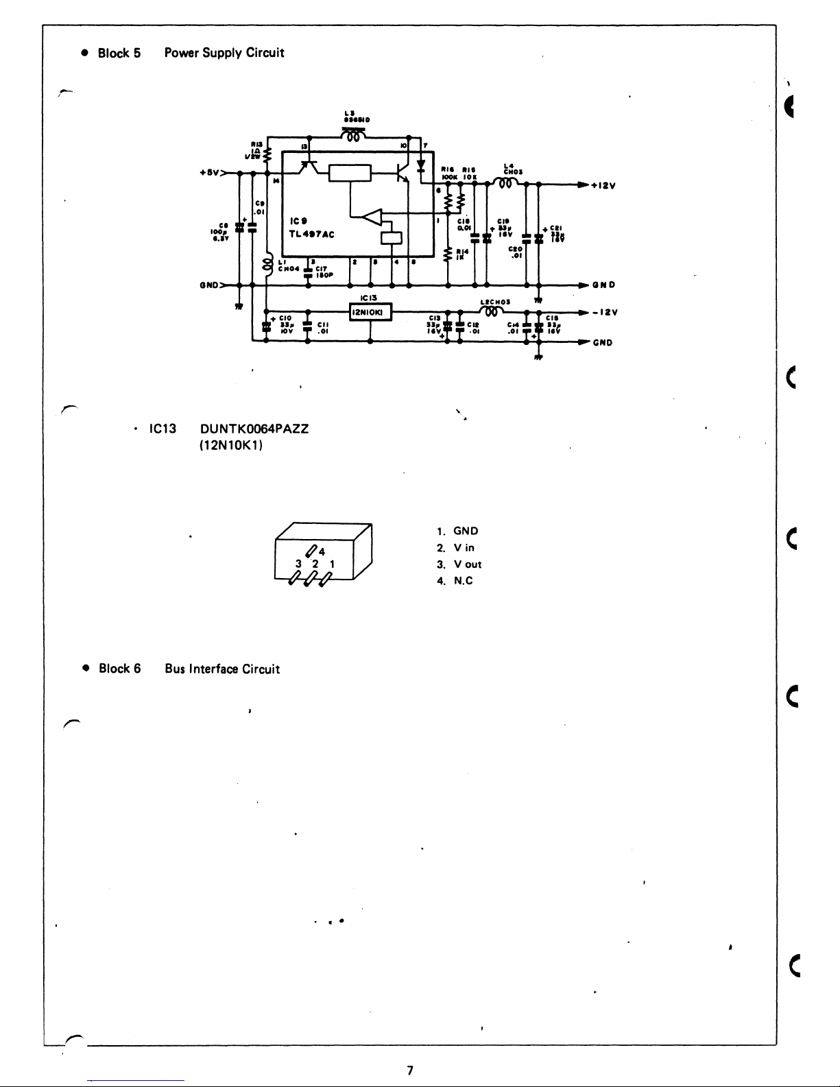
• Block 5
r
.
• Block 6
Power Supply Circuit
+
IV
ce
I~/.
aND
IC13
DUNTK0064PAZZ
(12N10K1)
LI
eH'"
~
LA1---V
Bus
Interface Circuit
.
..
+IIV
aND
cia
-IIV
U~
GND
,
1.
GND
2.
Vi"
3.
V out
4 .
N.C
~------------------------------------------------------------------------~
7
c
(
c
c
c
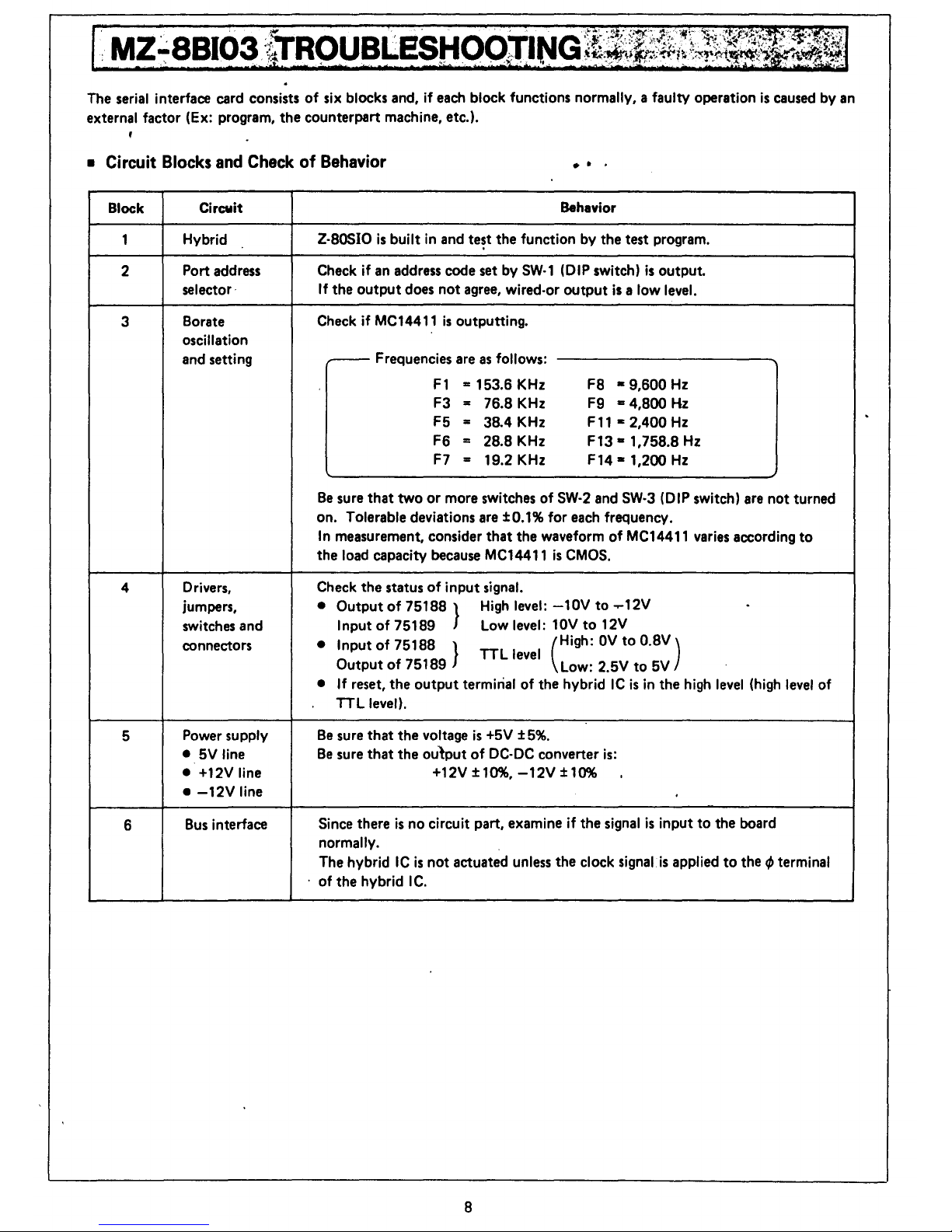
The
serial
interface card consists
of
six blocks and,
if
each
block functions normally, a faulty operation
is
caused
by
an
external factor (Ex: program, the counterpart machine, etc.) •
• Circuit Blocks and Check
of
Behavior
..
.
Block Circuit
Behavior
1
Hybrid
Z-80SIO
is
built
in
and
te~t
the function by the test program.
2
Port
address
Check
if
an
address
code
set
by
SW-1
(DIP switch)
is
output.
selector·
If
the
output
does
not
agree,
wired-or
output
is a low
level.
3
Borate
Check
if
MC14411
is
outputting.
oscillation
and
setting
r--
Frequencies
are
as
follows:
F1
.. 153.6 KHz
F8
• 9,600 Hz
F3
..
76.8 KHz F9
..
4,800 Hz
F5
..
38.4 KHz
F11
.. 2,400 Hz
F6
..
28.8 KHz
F13·
1,758.8
Hz
F7
..
19.2 KHz
F14·
1,200
Hz
Be
sure
that
two
or
more switches
of
SW-2
and
SW-3
(DIP switch)
are
not
turned
on.
Tolerable deviations
are
±0.1%
for
each
frequency.
In measurement, consider that the waveform
of
MC14411
varies
according
to
the load capacity
because
MC14411
is
CMOS.
4
Drivers,
Check the status
of
input
signal.
jumpers,
•
Output
of
75188 }
High
level:
-10V
to
....
12V
-
switches and
Input
of
75189
Low
level: 10V
to
12V
connectors
•
Input
of
75188 }
Ci9h:
OV
to
0.8V)
TTL
level
Output
of
75189
Low: 2.5V
to
5V
•
If
reset,
the
output
terminal
of
the hybrid
IC
is
in the high
level
(high
level
of
TTL
level).
5
Power supply
Be
sure
that the voltage
is
+5V ±
5%.
•
5V
line
Be
sure
that the
oulput
of
DC-DC converter
is:
• +12V line
+12V ±lO%,
-12V
±10%
0
•
-12V
line
6
Bus
interface
Since there
is
no circuit part, examine
if
the
signal
is
input
to
the board
normally.
The hybrid IC
is
not
actuated
unless
the clock signal
is
applied
to
the
q,
terminal
of
the hybrid I
C.
8
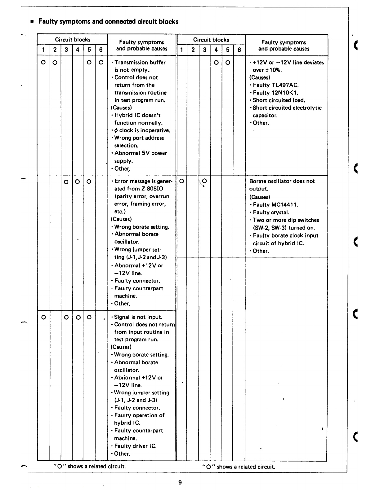
• Faulty
symptoms
and
connected
circuit
blocks
Circuit blocks
Faulty symptoms
Circuit blocks
Faulty 'symptoms
1
2
3 4 5
6
and
probable
causes
1
2 3 4 5
6
and
probable
causes
c
0
0
0 0
o Transmission buffer
0 0
o +12V or
-12V
line deviates
is
not
empty. over ±10%.
o Control
does
not
(Causes)
return from the o Faulty TL497 AC.
transmission routine
o Faulty 12N10K1.
in test program run.
o Short circuited load.
(Causes)
o Short circuited electrolytic
o Hybrid
IC
doesn't
capacitor .
function normally.
• Other.
o!p
clock
is
inoperative.
o Wrong port
address
selection.
• Abnormal
5V
power
supply.
o
Othe~.
(
0
0
0
o Error
message
is
gener-
0
,0
Borate oscillator
does
not
ated
from
Z·80SIO
•
output.
(parity error, overrun
(Causes)
error, framing error,
o Faulty MC14411.
etc.)
o Faulty crystal.
(Causes)
o Two or more
dip
switches
o Wrong borate setting.
(SW-2,
SW-3)
turned
on.
o Abnormal borate
o Faulty borate clock input
.
oscillator.
circuit
of
hybrid
IC.
o Wrong jumper
set-
o Other.
(
ting (J-1,J-2
and
J-3)
o Abnormal +12V
or
-12V
line.
o Faulty connector.
o Faulty counterpart
machine.
o Other.
0 0
0
0
•
• Signal
is
not input. c
-.
o Control
does
not return
from input routine in
test program run.
(Causes)
o Wrong borate setting.
o Abnormal borate
oscillator.
o Abnormal +12V
or
-12V
line.
o Wrong jumper setting
(J-1,
J-2
and
J-3)
,
o Faulty connector.
o Faulty opel'1ltion
of
hybrid
IC.
o FaUlty counterpart
,
machine.
(
• Faulty driver
IC.
o Other.
..
0"
shows
a related circuit.
..
0"
shows
a related circuit .
9
 Loading...