

Page 1
SHARP
SERVICE
MANUAL
PDSMX81014-MZ
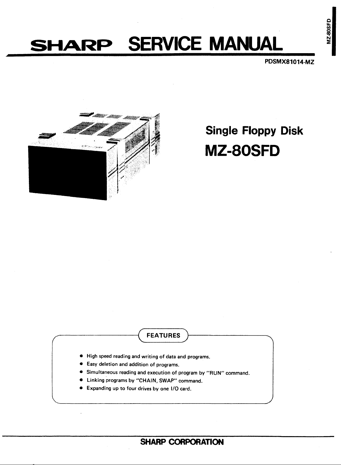
Single Floppy Disk
MZ-80SFD
FEATURES
• High
•
• Simultaneous reading and execution
•
• Expanding up
speed
reading and
Easy
deletion and additionofprograms.
Linking
programsby"CHAIN,
to
writingofdata and programs.
four
drivesbyone
SWAP"
SHARP
of
programby"RUN"
command.
I/O
card.
command.
CORPORATION
Page 2
------------Contents--------~'\
Specifications 1
of
Constitution
Operational principle
Inspection and replacement
Trouble shooting guide
Power supply
Circuit diagram and printed wiring board 15
Packing method . . . . . . . . . . . . . . . . . . . . . . . . . . . . . . . . . . . . . . . . . . . . . . . . .
Disassembled views ' . . . . . . . . . . . . . . . . ...21
Replacement parts list . . . . . . . . . . . . . . . . . . . . . . . . . . . . . . . . . . . . . . . . . . . . .
single floppy 1
of
floppy disk " 2
of
section.
disk drive main parts . . . . . . . . . . . . . . . . . . . . . . . . .
. . . . . . . . . . . . . . . . . . . . . . . . . . . . . . . . . . . . . . . . . . . . .
..
..
..
..
11
13
20
23
6
Page 3
II
r$PE.qlf1t"iiO~$
I ·General specification.
(a
humidity
out
prior
such
partially
Specification
maximumoffour
(freeofmoisture condensation)
notice
cases,
items mentioned above may be
different
drives)
for
product improvement. In
from
the product.
to
change
--_.
--
---
---
with-
---_._-
------
--
Item
--
-----
AC
220V
AC
240V ±
DC 12V
DC5V
-
-
± 10%, 50Hz
10%.
50Hz
Daisy-chain system
5.25-inch both-sides flexible disk
Double
Soft
280K
140K
AC
AC
30W
5
20
Approx.
4
or
single density
sectored
bytes/driveat16 sectors/track (double density)
bytes/drive at 16 sectors/track (single density)
220V
± 10%, 50Hz
240V
± 10%, 50Hz
to
25°C in temperature
to
80% in
165 (W) x 102 (H) x 323 (D) mm
kg
* Specifications and design subject
1
>------
-----------------------
1----
• Power supply section specifications
Drive-to-drive connection
Recording medium
Recording
Numberoftracks 70 tracks
Sector
Formatted capacity
Power supply
Power Consumption
----
~._-----~---_._--
Operating conditions
External dimensions
Weight
Item Specification
Input
Output
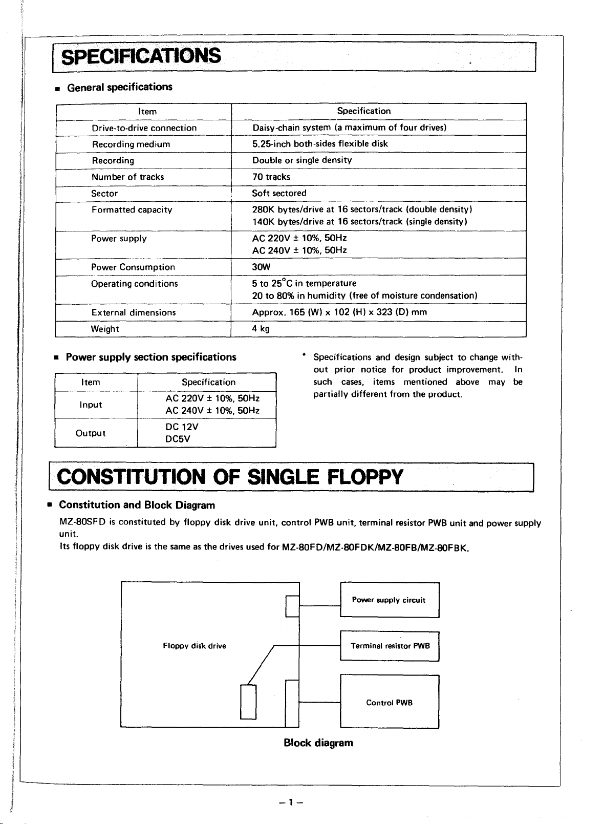
{CONSTITUTION
• Constitution and Block Diagram
MZ-80SFDisconstitutedbyfloppy
unit.
Its
floppy
disk driveisthe
sameasthe drives
Floppy
disk
OF
disk drive
drive
SINGLE
unit,
control
used
for
MZ-80FD/MZ-SOFDK/MZ-80FB/MZ.SOFBK.
[
r--
-
Block diagram
FLOPPY
PWB
unit,
terminal resistor
Power supply
Terminal resistor
Control
circuit
PWB
PWB
PWB
unit
and power supply
-1-
Page 4
_O_P_E_R_AT_I_O_NA_L_PR_I_N_CI_P_LE_O_F_F_LO_P_P_···.·y_·.····O..:....-.'
The
floppy diskisdesignedtorotate
"diskette,"
and write in dataathigh speeds
a magnetic disk storage unit,toread
the
by
bringing the
so-called
out
in
direct
magnetic head
sector of 70 tracks formed in
diskette.
contact
...........
$Kw...···
••.
>............... J
witb a specifil!d track
both
surfacesofthe
1. Fundamental block diagram
Read
Write
Write gate
Write
protect
data
Head select
data
Read circuit
Drive
select
Write circuit
Write
la,*/'
Operation
.
d'
In
Icator
/'
0'
-~~
protectr"··"
)-1
(}--:":":'..,..-----""'1'---------.
Write
./
protect
senso!",
,/
,-!lr
IndeX~-'l'--
sen_s~:JJJ'
~
Head load-
.
.,
actuator
I
--'
__
Direction •
Track
...
..,;D~r;;;;iv;.;.e;..s::.,;el;.;.e-ct--f
Head select
Motor
2. Mechanism explanation
This device consists mainly
mechanisms.
1)
Read/write head
The head
spring.
diskette easily.
Signals read
through FPC (Flexible Printed Cable)tothe
amp. circuit.
2) Carriage assembly
2 units of read/write head are
carriage. The carriageislocated with
motor
3)
Head locating mechanism
This
mechanism using stepping
ball/V -groove system.
The
type.
One pulse of
by
15
L..-
track.
is
The
and lead screw.
is
a high-precision, reliable head locating
stepping
0
, thus pushing forward
1.-..--..----,...-'
Head select Head load • •
s_t_e;..p
__
--.1,.......L--L--L..,I-
Index
00
ON
attachedtothe
head can follow
out
motorisof
step
Control
of
the
signal causes a 2-step
circuit
of
arm
head are
mounted
motor
and screw-driven
7.5°/pulse, steel
the
the
through
the
transmitted
the
head
Index
I~
Motor
1-
__
following
a leaf
motion
read
on
stepping
plate
rotation
by
one
ON
-,
of
the
,I
. .
~.
Rea1/write~"""
~d
Diskette
Motor
control
circuit
41
Diskette driving mechanism
A small-sized
employed. The
through
hub, thereby causing
spindle pulley
check
5) Head load mechanism
This
into
the
._~
•
..".
~:I:
\t==:INIJ.-1IlrJ
'.
DC
motor
motor
the
drive belt, spindle pulley and spindle
is
provided with a stroboscope
rotation interval.
is
a mechanism in which
contact
head load actuator.
with
.
the
with tacho-generator
rotation
rotationofthe
diskette. Itisoperated
is
transmitted
diskette. This
the
headisbrought
~
__
~
to
by
is
_
-2-
Page 5

6)
Write protect detection section
A luminous diode and a photo-transistor are used
to detect write
jacket. (Writing
protect
is
notchofthe diskette and
not
possible when
the
notch
covered with labeL)
Center
hole
Label area
Write
protect
notch
3. Interface
1) Interface signal
All
lines areofTTL (transistor-transistor logic).
is
(1) Input signals
of
For input signals there are 10 kinds
input lines,
allofwhich are validatlow levels. These signal
lines are terminated
resistor fittedinthe
signal voltage levels are
High
level
Low level
Invalid 2.4to5.25V
I
Valid o
I
Input impedance
a 150-ohm
IC
socketofdrive1.The
as
follows.
to
OAV
Pull-up
to5Vat
int~rated
150-ohm
at
resistor
Head
window
Description
7)
Index detection section
This section consists
phototransistor. An index hole
Index
hole
of
diskette parts
of
a luminous diode and a
of
the
diskette
detected by this sectiontodetermine the starting
point
of
a track.
8) Track00 detection section
is
A carriage position
the
When
track
9)
Control electronics section
carriage has reached the track00point,
00
signalisemitted.
The electric circuit
composed of 2 sheetsofPWB.
DC
the
control
motor
other
functions with respect
load, and
other
detected with a limit switch.
to
control each mechanism
Oneisto
control circuit. The
otheristo
circuits, say, detection and other
to
read/write, step, head
signals.
10) Diskette protect mechanism
the
Shutting
pletely set in, can give damage
shortening its life-time.
back, this mechanism has been adopted so
front door
front door, with the diskette incom-
to
the
diskette, thus
To
prevent such a draw-
that
connot
be closed if
the
diskette
improperly in.
control
the
CD
Drive select signals (0
MZ-80SFDisconnectable up
is
These signals are used
the
four drive units.
At low levels of drive select signal,
to
3)
to
4 units.
to
select a desired one of
RIW
head
is
loadedtocause the operation indicatortolight up.
Note)
The drive requires
to
switch
is
thru 4).
@ Motor
meet the position of use (Drive No. 1
ON
signal
The drive motor starts when
comes low. This signal
2 seconds after completion
to
be set with a drive select
the
signal level be-
level
becomes high about
of
all operations,
if
no operationiscommanded next. It thus inter-
the
rupts
motor, extending the service life
of
motor.
@ Direction select signal
The signal
direction
is
input.
High
Low
@Step
signal
This signal
direction designated by the direction select signal.
The operation
from low levels
is
given
to
of
RIWhead, when the
level- - .
Out
direction (to diskette
designate
the
step
portion)
level
- - -INdirection (to diskette center)
is
giventomove the
is
doneinthe
to
high levels.
RNoJ
courseofchanging
shifting
pulse
outer
headinthe
is
-3-
Page 6
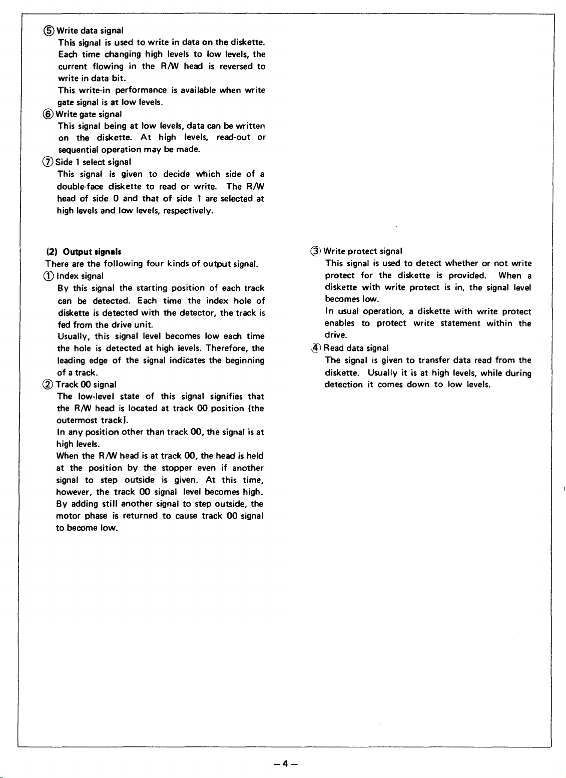
®Write data signal
is
This signal
Each time changing high levels
current flowing in
writeindata
This write-in performance
gate signal
@Write gate signal
This signal being
on
the
sequential
(j) Side 1 select signal
This signal
double-face
headofside 0 and
high levels and low levels, respectively.
usedtowriteindataonthe
the
RIW
bit.
is
isatlow levels.
at
low levels,
diskette.
operation
is
diskettetoreadorwrite. The
At
high levels, read-out
may be made.
given
to
decide which sideofa
thatofside 1 are selected
diskette.
to
low levels,
headisreversed
available when write
data
can be written
the
RIW
to
or
at
(2)
Output
There are
CD
Index signal
By
can
disketteisdetected
fed from
Usually, this signal level becomes low each time
the hole
leading edge
of
@Track00signal
The low-level state
the
outermost trackJ.
In
high levels.
When
at
signal
however,
By adding still
motor phaseisreturnedtocause track00signal
to
signals
the
following four kindsofoutput
this signal the. starting positionofeach track
be detected. Each time
with
the
drive unit.
is
detectedathigh levels. Therefore, the
of
the
signal indicates
a track.
of
RIW
headislocatedattrack00position (the
any position
the RIW headisat
the position by
to
become low.
other
than
the
step
outside
the
track00signal level becomes high.
another
signaltostep outside,
the
index hole
the
detector,
this signal signifies
track
track
00,
stopper evenifanother
is
given. At this time,
the
the
beginning
DO,
the
signalisat
the headisheld
signal.
track
that
the
of
@ Write protect signal
is
This signal
protect for the diskette
diskette with write
becomes low.
In
is
usual operation, a diskette with write protect
enables to protect write statement within
drive.
.~
Read data signal
The signal
diskette. Usually it
detection it comes
usedtodetect
protectisin,
is
giventotransfer
isathigh levels, while during
downtolow levels.
whetherornot
is
provided. When a
the
signal level
data
read from the
write
the
-4-
Page 7
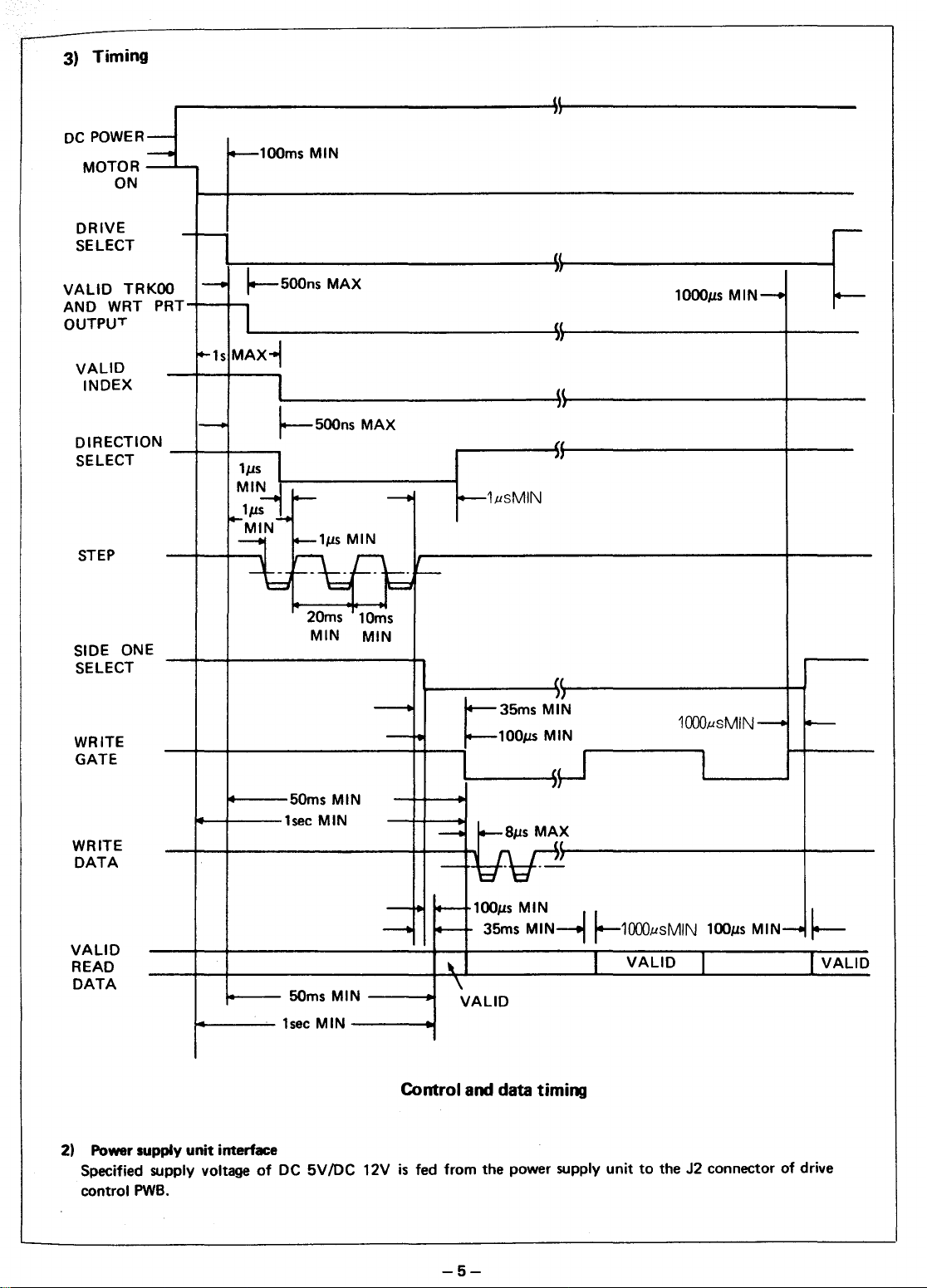
3) Timing
~\
DC
POWER
MOTOR
ON
DRIVE
SELECT
VALID
AND WRT
OUTPUT
SIDE ONE
WRITE
TR
VALID
INDEX
DIRECTIO
SELECT
STEP
SELECT
WRITE
GATE
DATA
-
-
KOO
PRT
N
-
-
--
....
1s
I-
-100ms
I--Soons
I
MAX--j
1J,Ls
MI~
1J,LS
-MIN
-
\
~
....
t:::j
MIN
MAX
~soons
~
4
1--1J,LS
-
MAX
--
MIN
'---
~~
20ms
MIN
10ms
MIN
--
-
..
SOms
MIN
1sec
MIN
~1tlsMIN
1:=35m.
100J,LS
-aJ,Ls
--
'd
~~
((
II
1/
II
u
II
{{
I}
MIN
MIN
({
II
MAX
"
II
1000J,Ls
1000tlsMIN
I
MIN-
-
1
[
-
100J,Ls
-~
if-
--1
VALID
READ
DATA
2) Power supply unit interface
Specified supply voltageofDCSV/DC 12Visfed from the power supply
control
PWB.
50ms
1sec
MIN
MIN
~
\
\
~
VALID
Control and data timing
-S-
MIN
3Sms
MIN~
100J,Ls
!--1000tlSMIN
VALID
I
unittothe J2 connectorofdrive
1
MIN-I--
I
VALID
Page 8
1. Belt
1) Inspeetion
to
see if
the
Check
Also make sure
beltisstained with
that
scratch and thinned part.
2)
Replacement
1)
Take
the
belt
off
the
the
pulley graduallybyhand.
2) For applying the belt,
motor
rotating
pulley and
the
thenonthe spindle pulley while
spindle pulley.
Note)
1.Inputtingonand
be
not
caughtbythe
2. Note
that
off
motor
thereisno
sidesofa new belt.
~
dustordirt.
there·isno
unevenness,
spindle pulley while rotating
put
the
the
belt, be careful so
belt first on
the
that
pulley flange.
difference between
Motor
pullev
Keep
belt
off
the flange.
both
2.
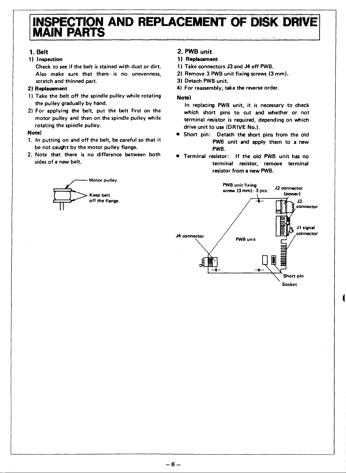
PWB
unit
1)
Replacement
1) Take connectors
2) Remove 3
3) Detach
PWB
4) For reassembly, take
Note)
In
replacing
which short pins
J3
andJ4off
PWB
unit fixing screws (3 mm).
unit.
the
reverse order.
PWB
unit, itisnecessarytocheck
to
cut
and
PWB.
whether
or
not
terminal resistorisrequired, depending on which
to
drive unit
Short
•
it
use (DRIVE No.).
pin: Detach
PWB
unit·
the
short pins from
and apply
them
to
the
a new
old
PWB.
• Terminal resistor:
If
the
old
PWB
unit
has no
terminal resistor, remove terminal
PWB.
fixing
3 pes.
,...--'0-----=--1
unit
J2
connector
(power)
J3
connector
J1
signa'
connector
J4
connector
resistor from a new
PWB
unit
screw(3mm):
PWB
Socket
-6-
Page 9

3. Index lamp assembly
1) Inspeetion
CD
Connect power sockettoconnector J2ofPWB
unit. Turn power on.
®
Make
sure
that
thereisa voltage rangeofDC1to
1.7V between
pin from power socket) and
the 11th pin from power socket), both belonging
to
connector J3.
B-11
(lower white lead of the 11th
A-11
(black lead
of
2) Replacement
CD
Remove
® Disconnect 2 lead wires
from the housingofconnector J3.
@
Cut
lamp assembly (be careful
wires), and open
@)
Take lead wires off the guide groove of carrier, and
draw
and fingers.
®
To
® Carry
left.
Index
lamp
PWB
unit (refertopage 6).
of
index lamp assembly
off the tie band fixing lead wiresofindex
nottodamage lead
the
front door.
out
the index lamp assembly with tweezers
attach, take
out
assembly
the
reverse order.
inspection, referringtodescription at
Note)
When
attaching
carrier, fit the housing and
time.
the
index lamp assemblytothe
LEDinat
the same
-0
-7-
Page 10

4.
Media guide l assembly (with write
1) Inspection
ill
Connect power sockettoconnectorJ2of
unit. Turn power on.
@ Before inserting a diskette, check
items.
a)
Write protect lamp
Make sure
to
1.7V between
13th pin from power socket) and A-13 (black
leadofthe
belongingtoconnector J3.
b) Write protect sensor
Make
to
O.5V
14th pin from power socket) and A-14 (black
leadofthe
belongingtoconnector J3.
that
thereisa voltage rangeofDC
B-13
(lower yellow leadofthe
13th pin from power socket), both
sure
that
thereisa voltage rangeofDC
between
B-14
(orange lead below the
14th pin from power socket), both
the
@ Put a write protect diskette (with write
seal being applied at the write protect notch of
diskette)inplace, and shut the
check
the
following item.
• Write protect sensor
Make
sure
that
thereisa voltage rangeofDC
2.5
to
5.25V between 8-14 and A-14
connector J3.
front
door. Then
protect
PWB
following
protect
of
sensor lamp)
1
0
2) Replacement
CD
Remove
PWB
unit (refertopage 6).
@ Open the front door.
@ Detach 4 lead wires
from the housing of connector J3.
of
media guide L assembly
@ Remove 2 media guide L assembly fixing screws
(3
mm) and take
out
the assembly.
@ To attach, take the reverse order.
® Carry
Note)
1. Attach the media guide L assembly by pushing it
2.
out
inspection, referring
left.
to
main frame stopper side and front bezel side.
Lamp and sensor cannot be individually replaced,
because they are built
assembly.
to
description at
in
the
media guide L
Push
Media
guide
L assembly fixing screw
Media
guideLassembly
Main
frame
stopper
Write
protect
Front
lamp
bezel
-8-
Page 11

5. Operation indicator
1) Inspection
CD
Connect power sockettoconnectorJ2of
PWB
unit and turn power on.
(Z;
Let drive select 0ofinterface signals beatlow
levels (make a short between J1·B terminal
and
PWB
Ground). and make short pin
circuit shorted. (Do
Note
that
the voltage range between connector
J3·B10 (red lead of
socket) and J
pin from power socektl will be
the lamp
2)
Replacement
CD
Remove
is
PWB
lit.
not
prolong this test.)
the
10th pin from power
3-A
10 (upper black leadofthe 10th
DC1to
unit (refertopage 14).
of
PWB
DSO
2V when
@ Datach 2 lead wires of operation indicator from
the
housingofconnector J3, and take lead wires
outofthe
CID
Open
@)
Remove 2 front bezel fixing screws (3 mm) and
the front bezel itself by pulling it forward.
@)
Draw
direction. Take
right.)
@ Draw
take the reverse order. .
(j) Carry
instruction.
wire holder.
the
front door.
out
the
holder 2 with tweezersinthe
out
LED
outofthe
out
inspection, referring
LED
holder. (See the sketch
LED
holder. To assemble,
to
the above
arrow
Front
bezel
LED
holder
Pull-out
direction
at
Note:
1.
Attach the
front
bezel assembly, by pushing it
to
main frame side and main frame stopper. (See the
sketch below.)
2.
Do not pull up the carrier with fingers, otherwise
excessive force
is
appliedtothe
head arm.
Main frame side
Front
bezel
Front
door
-9-
Main frame stopper
1)'
Push
Main frame side
Front
bezel
fixing
screw
Page 12

6.
Drive
11
Inspection
<!>
Connect _
"";t.
(%ll.ed
lmab
_
motor
T
....
in,
..
.01'>
PW8
assembly
__
face
mol..ON .i!lnols be
...
bel',,""
Groundl
>ocr..,
Oft.
JI·16
and
IDe
'0
cannectot
l......
run
mOlor
iNf
tIM
mol
and
n
of
a,
low ....e/s
0'
PW8
...
100
mOlor
PWB
uni,
....
,
cortl.al
PV/e
21
<D
<2>
<:p
unill
Rtplocemonl
R
....
Put
Cu.
_
d
.....
.-
off
1M
olf
tIM
mol<><
lead
PWB
""il.
bfoIl.
,iI
bind
eont.....
.....
CR.'
...
to
lR,I..10 _
I
..
fi
.....
fIWB
pogo
unit.
6,1
Iud
lk
6.1
wi
...
_,lui
of
......t
nol
..
to
prolong
<])
Pul.
@
amy
(8)
Make
•
pindl.
Note)
The
oIIiftiflll
to 1.5 pc;..M.
,his
dish".
on
hod
.ur.
pulley
,-.1
'11"
,ata
I"'"
In
p1_
load.
III.
.ppo
olwol>oplale
and
moboplate
...
10
V.._-",_
__
clme
be
.tationary.
is
...
1M I<on,
attaclled
allowflj to
_01
......
<100<.
on
be
_'
.........6.....
IIII'
""
<!>
A_
<:on1r01
ing
tID
R.m"".
13
Ootacll
'rom
@}
For
CV
Catty cu,
"".
P\W
of
""""oct
2
mml
ar>d
the
Ih.
mlin
auernbly.
3
Iud
u
J3.
met
2
DC
DC
meto,
frame.
tak.
insI>ection.
.ir........,..,.'"
10
conntlC<Of
tontrol
motor
tho
and
,,,,,er.
PWB
fixing
molD'
,.,.ttinll
t......
JJ_lrom
Unil
fixing ocrew.
OC'I'WO13mml
oontrel
ord.,.
to
....."iption
tM
1M
PWB
motor
I>ooJs.
.
unit
al
No•• l
In
.pl""I.
be
mOlJnlI~
pull.y
73
.iOA
'III'
mm"'III<Iwn
DC
mOlD'.
and mOtor pulley
abo
til.
••.
dl.tl~
.hould
be kept to
bet,veon
_10_
3f
Adju.'mon,
Q)
Alto,
Idiu"
unit
p1llely
,h.
cOmpletion
the
...
'"
,hal
Ilatio"",y
ilbl.,••
'1>0
ltroboplat.
of
i"",
th.
lbo
••
0'
molD! controf
appe_l
chock ilom
PWB
10 be
tom·
•.
Page 13

[
TROUBLE
SHOOTING
Startofdisk system
GUIDE
Yes
~--------'~
Yes
No
End
• Check by replacing several sheetsofdiskettetosee if errors occur duetofaulty diskette (data deterioration
caused by foreign matters, deformation, wear-out, damage, magnetism, etc.).
• Troubles
• Replace suspected parts
• The signal circuits of floppy disk and I/O card operate at TTL levels of
micro-computer peripheral devices for MZ-80 series
+5.25V).
• The disk drive needs a
it must be expanded.
in
disk system often cause error messages. Trace the cause from the contents of error message.
in
the disk system with normal ones. Check again the trouble section.
1)
Personal computer
2) Interface unit or expansion port
3) I/O card
4) Diskette
5)
Signal cable
6) Disk drive
RAM
areaofmore 36K bytes.Ifthe
Check repair procedure for power
supply section.
(See pages
Trace
of
to
seeifsignal levels are
13 and
14.1
the
cause from
error
message. (See page
OV,
+5V. Connect any system other than
RAM
areaofyour machineisless than 36K bytes,
the
contents
12.1
out
of the range of 0
to
+5V (max.
-11-
Page 14

• Error
chart
for disk system
Error code
[Error message]
1)
50
[NO READY] a Diskette
Drive fails
to
is
a Motor does not normally run.
a Index detection circuit
a Flat cable
a
No
is
select signal comesatdrive.
a Drive unit door (front door)
closed.
a Diskette
is
a Write operation
protect state.
1)
54
[UNFORMAT] a Head position
Drive
(off-track state)
a Head and amp. circuit are defective.
2) Diskette
a Diskette not formatted
41
[DISK DATA
ERROR]
a CRC error
a 10 field
1)
Drive
a SEEK error
a Head shift
in10field.
is
broken down.
is
Contents
be ready.
wrongly inserted.
Check item and corrective action
a Fit diskette in correctly.
a Check belt and/or drive
is
improper.
improperly fitinor
broken.
a Check index lamp, drive
a Check flat cable.
a Check floppy disk I/O card.
is
not
faulty. a Replace diskette.
is
attemptedinwrite
is
not
aligned. a
isinuse.
a Close front door.
Replace drive unit.
Replace drive unit and/or drive
a
o Initialize again, or replace diskette
a Check drive unit and diskette
Replace,ifrequired.
improper.
a Replace drive unit.
motor
PWB,
assembly.
index sensor.
PWB
unit.
2) Diskette
a CRC error
a Data field
a 10 field
in
data field.
is
broken down.
is
defective.
a Data mark detection error.
iO
Initialize again,orreplace diskette.
-12-
Page 15

!
POWER
Block DiagramofPower Supply Section
supplv
SEcnON
.---
~
'-'
AC
INPUT
'-F
WaveformofEach
..
Gl
~
I--
LL
"--
Waveformofpin@ofIC201
and
pin
(5)
..---
..
Gl
E
..
~
c
..
..
...
:......-
of
t--
'---
Part
IC301.
Rectifying
Smoothing
Circuit
'"'-
Rectifying and
Somoothing
Circuit
and
~
Waveformofpin
([j)
Transistor
Chopping
Circuit
Transistor
Chopping
Circuit
of
IC201.
Control
Circuit
1
Control
Circuit
1
Q202 collector waveform.
+12
...-<>
+5
v
G
~
v
Waveformofpin
([j)
of
IC301.
15V
/-22~s-i
40~s~
0302
collector
15~s
waveform.
40~s
I
22V
22V
24~s
4(j~s
-13-
Page 16

•
Trouble
Shooting Chart
Problem 1: No voltage appearsatany
~
Is
there AC
for U.K.I present across
C101?
220V
(240V
V~
Problem 2: +12Visnot
Is
there AC
present across
red lead
20V
the
of
n01
7
Nrl
I.-
Check
developed.
n01.
output
Check
AC
socket,
AC
switch
N~
terminal.
AC
Check
COrdi
F101,
F102
and
C101.
n01
Check
0201
~
Check IC201
Check
circuit.
appear
peripheral
~
r---
V;:
Leave R203beopen;
does
there
1Vp-p pulseatpin
No.
11ofIC201.
output
f---
and
parts.
switching
its
V~
present across
Problem 4: +5V is
Is
there AC
present across
yellow leadofT101 7
14V
the
n
L-
Is
present
V~
Is
thereDC20V
not
developed.
Check
n01.
thereDC14V
across
C2027
C302?
.--
f--
V~
No
r-t
V~
Does waveformofthe
chart
appear
collectorofQ2027
Check
Does waveform
chart
appearincollector
of
03027
in
0301.
of
~V~
the
t---
Yes
~
Check L201
C205,C209.
No
r-
Yes
Leave
R303beopen;
there
does
1Vp-p pulseatpin
No.
11ofIC301.
Check L301, C305.
and
C309, C310.
and
~
appear
Check IC301
peripheral
Check
switching circuit.
output
f--
and
parts.
its
-14-
Page 17

...
...
...
o
co
CD
"'"
0)
U'1
~
eN
~
....
I
...
U1
I
&T~~~lmA
,
I
I
&:
SWlIOI
&
C'O'
I
o.047J1neovAc
I
I
I
&f~~mA
Parts marked with " & " are
the
safetyofthe
specified ones for maintaining
mance
of
the
set.Besuretoreplace these parts with
set,
important
the
safety and perfor-
.6
TIOI
r--------,
, • I
L _
for maintaining
J
II
~:>
I
II
~>
IIOOV
I
0.-,
~>
~.Ol~
~
~>
:
..
~>
f
)c::>
I
)c:>
I
O.l,,~~OJ
RZIO
I.IIC
10
D
:
I
OJ"
~IOOV
I
:=
~
~
I !OOOJI/2SV - -
~
010'
4 SIV810 J
>
.a
~ao.
:
4.1IC
:
C~I~
010'
l
IIV8IO
rI"
II
II
If
II
II
II
"
II
II
If
II
I
II
II
II
II
II
II
II
II
II
_.J
>
RI,O
I.SIC
nr
:
:
:.~:-
VRSO'
o.,,,etS:~
'OO~~~
M04~
2.Zte
4
~
II
,
MO"
~
4.1IC
n
-
~
'U04
..
2.21C
l~
,.
I 2
RJ07
4.ne
n
II<
RIDS
IS
14
2 I
~~~~
RIll
'SK
C102.
Itl0S
411C
15
14
S
It
101
410K
It
lit
S.tte
( J
TL494CN
.f
TL494CN
.~I"¥
'00
rUOS
.!OOOJI
CIOe
IS",.
~
'I
IC201
r
0.0..,/5OV
.I~CIOS
t
~~
CSOI
sa,,/1
~
IS
IC301
e201
IS5V
V
12
~
:=
125V
IV
'I
"
I
~1tlO.
2{te
l.Ck
II
RIOt
1.71<
10
T
'00
.~
~'r.
. CS04
10
.,
J:
1t10i
2i,.1tt.
T
r
O.O,."/SOV
CIO'
2.H
0201
ArrOY
g
~
020~~)
A673C
CI04
0.00'1'
Iti0S
I.Tte
•
I
~
0301
A770Y
¥d
~
0302
ItSOS
2.11C
•
1
L.-
).
0.00'"
~
: =I
~
~
11M
V
0101
IIt"'-00412
~.
I.",
110
DIGI
I:R'''-OO412
L201
ZOOO7
roo
I
It
~
DIOS
zoom
~
I • +
V
UOO,.II.IV
Dioa
+
JI_·~I~
...
"IV
RI'I
O.'AI2W
csotVR20'
O.OI"/IOV
.1_
ItSIr
o.'AI2W
::
001"
eS05
~caoe
:
!!>D.a"IO
:=
cs
'0
tiel
;',(1.>.
...
z
•
:.
o
•
-a
o
+12V
-
-
~
JO.
V
GNO
+5V
i
..
en
c
-a
'"0
<"
n
~.
;:;.'
,...
(t:)
en
--I
...•
c::
[<!:::Ii
"
..,
K<d
a.
OS'
-
lO
.....
.,
OJ
ill)
3
Q)
::::J
;,1·
C.
~
.,
:i"
~i~):E
,...
(t:)
c.
~"
..,
.-
:i"
(Q
Z
CT
o
Q)
..,
a.
•
OJ
(il
en
~
c:
....
C"
:z
(b'
~
,..
--I
o
o
1ft
::r
OJ
::::J
a
~
~
;::+'
::r
~
o
c:
,..
"C
..,
•
-
cS"
z
..,
::::J
I)
o
,..
(=i'
~
CD
»
a:J
o
o
m
-n
G')
o
»
:rJ
'0
J:
Page 18

A B
c
o E
F
G
H
1
2
•
Power
Supply
PWB
3
4
5
6
Primary
7
8
9
10
F0410PA
Secondary
11
-16-
Page 19

A B
c D
E F
G.
H
I
J K
L M
N
o
P
1
2
• Disk Drive
HEAOO
R/W
ERASE
PWB
.~
~
I
r I
:
I I
>_'H:'g:~J4~-~A~3:::+~*'
Circuit (Reference diagram)
,J4:!:!:-A!'.!.7
,I
'T
IA
tl
J4-A6
J4-A5 3.6K
J4-A4
C2
10.u
"""-I
At
09
,,-_
05
::
D~I
Vj
D
Yr-
---1r-
[;:7t-'j---j-_
v
.'--=
r--J-;
'Lj---t"
:06
r
15
C3
~
RA GND Vee 1
17"
,,0.01"
v I C5
------,,;:04 I
~.--=:-r_-----'''13
108
I 16PIN 0 4 V
14
AS
WA
f:01B4392
1.
"J4.Al
v,
r
~
.D'
'2
116
ITp@)
+5V
A'-'-jf-----i;;>---j-..l--{;J--'""1=<
C4 R20
47~Op
330
A21
Bf2~4,7'IOO;r.P-<3=30J--k_-<6=8::>0_-i47Op
C 3
II
ffP28]'TP2AI
[!p@
R6
680
AS
C6
(TPGI
-
~+5V
r1
AN3,
4.7KL.f:,J3
,...;9~28pe::.8--c4~1:3iEE""}6"___!-___I-___I
LS04
rS'-<l~3~8//
1
.:
12 11
13
1~
~:
10 2
V
07
3E
,_-_
__
680
1
680
=.,-
AN1
RN2
7K
4.:.:.:. 3
_
2SA883
4
7K
.
..r:-'::.
3 4 -
1.#
'1
01
-+5V
1.2K
4~-
'--
1.2K
ANl
5
AN2
'K
-~6
':..JIfh,
lK
_.
6
3
4
HEAD
R/W
ERASE
1
~~
J4-B7
, "
, , f--
: :
I I
I I
(
~'"
:'6-~J4~.B~3L+~'f.',0-"__i.
, 4 Bl v
L"
J
""4,,,-Be>6,-,
1~J4,,_B,,-,,-S_+-_~_3_.6_K_j---
r-
J4-B4
J -
J
I J3.B13 7 5
4
.
A2
-
ntT
C1
-J,.
v,
L-----+---r--.-=
R2
-----'
,,),t','D:!..'!.':Oc-l-_-i3Ck-:i1~I..J
-r
8 ,
:,
ri
~:
U'fJ1S0;
'SV
,RN6
~
1
I
RN5
47K
RN3'
.7
L~'
~K>--l.!E~G~~S~~~C
R9
43
('hWl
T,
+SV
T'TP'"'
l.l..C!J
+5V
l
_,02
J.
'I'
Il11T
±
'T'
1l11T'
....
1
,AN7
I:
C13
001
G14
0
4.7K
I
. "
01p·
452
~V
r::;7,:505-I~'~'
R3
"1"2f-"'°"l'ffi
WA
WG
INS
IF
RS
C7
E 5
l000p
4-
F 6 T
L1
82{)pH
'~.·R7
430
AS
430
~
Dll
I
fEG)
(WGrl
__
~f-
+._+.
,4A
,w
LS05 9 8 1I 52
l~=J:!=~~~f=~====~==~~======t===~=~J
6 - - r 2
(PRl
"-,r--'--------+-+--
7 (EG)
-+-.1'-----
t---t------+-----==--"-'------t-----'
--t------=:'-:-----,--t------'-"-'
{WPI
(PAl
(WD)
l 9
............
:e"8~..:5'-j4~,'>_:6'_-+___,r_--2-;:c2S,,A-"8B=3."-.----------JS
?L:S04
__
CO",-+---j
38
/07
~.t====j-t--<31"-">4-:c:-r-t'2'i
·~'+--c;-<:c"-o--.-I----;7'·'_4_-S2-_-:
__
~
4S
/"
--
LS04
~
02
...
----
I B
.,
48
__
.....
:3
Pi-''-,---;--:;r==--
-=-.,J,
I ..J>15 I
_.J"j"
,,,.
STEPPING
MOTOR
J3·A5
_-fYY"L-,¢A
):>i'13,----,.,_:·~'J-"J3~-A~6~__6_-..rYY1.___l.8
~D16
I
~
'-----"<1>,!9C>::':r-r-tr--:-:::T'+.
r 1 ¢
11*f1
-=L"S:::04-=---t_L'-<.j'>--.10
:C;04
L_'.
3
r>:126
6
,
I
1
8
452_~:
;,
S
I .
~I
..
.D17
J3-A7
__
,..,.n_~
I C
~~B~~j'J!Sl----..=~·'~rJ:!'3!:'.8~7'-1-f'<rY''-~
_452
_-:
I
~
';"1
¢O
q
r;:-:
....,..,.-----
5
WRITE
PROTECT" J3-814 w
SENSOR
INEDNESOxR.----o1
S
r:-
~
Y n
t;:
I
J3-A14
I
J3-A13
J3-811 5 3
I
=J:3~-8~'~2~==
'-J3-A'2
.06~+5V
O:·=~
i5
'-----0
TRACK
SWITCH
00
I
J3-A9
I'
; 1
__
R1S
680
38
._
RN6
,50
"
..
~i:
.......
;r
I'
: L
+_''_'3q''113B12
All
680
~:.z,,>06"-----'S:.q'3Q>'6'----~4'-----..j.--__i-t31:"IC'~·
7lS14
RN?
~47K
?LSI.
10
lS14"'" j
3~
/LSOS
~
(If.~,
INDEX
--+-------·:..:.'---Il'-J-S~51-+-+1r---,
11
11 '-----I:::J---
~"
. LS05 12
r
12 L 13
~
(INDEX)
LS04
t----""l'r;s
VlS04
13
10 (WG) +5V 15 14
L~02
C"5:F~
-1m
10
, 9
3C
lSOo/
8
TOO
i A23 LS123 L .
820
l.-<=-r!.rl
r
10;;c::~;2~EJ'
'6 7
D19 LS123
~6gK
5
...
2-.:9q'
2S
8 r
399';;'1_+____i~-+____i~r---!.!(I~R'"D'.:'V~I____i~+_+-+__+-_,
"'1..505
-+5V-r-
t--=':...P"R:...'
+--+_'
'+C8
A4
47K
2 2E 4
__
____'3 v r
:::'F4.7pF
,,.l.
i
1111
03
2S860,
r----
,I
: I
..
t:
[...l
3~tO,::74'--+-+---I-t-~D
....
-.t·---I-I.,(_n)1I1+
~~4
~.~~F
i.;~F
"I
,,,
lS04
-,
I - I
.-----------'
-
D1S
,.
1_.-+12V
+12v-r-
D12
-C''!W~P:'I.l'-'2,i2"''
+5V
'-J,,3"'-B"'S'---o-~----j
'
J3·86
83
J3-
J3-81
J3·62
JfI
----:},"'-'~,~U2~AJ-~I~I~J,,'..:-2"'8'-?
IDS
13
38
'r:;
--o
+12V
I
.AI
0 MOTOR
DRIVE
I
WRITE
I
PROTECT
6
7
NO
NC
MOTOR
HEAD
SELECT
tu:C>--O---""
--A
·---·~~·__nk~81r4
ON
ONE
o
0-=-'
J3-A8
T
J3·B9
J'·16
1 Jl-4
0
..:.:--=----0
1
J'-32
..
0 ..
--r'------------
n
13
I
150 I i
1
HL
11
2'
Dj-~--;::::==I==i._.-+--+-.--.--:-:c;:---t--+--+L'
....
c_
--.
-j
H
-----------'
~
....
HI'
8
-+5V
AN6
150 1 2
,A_
,~
-"~~-1
I r I I
,
i i i
__
IRN4
41K
rs
+
__
-'4~~LS':"')/~
I,'
(PAd
l'I'~!--!l-.l",'C~'
~,-.
'--+--.
3C
"6
l
C26;J;;
-l-
11
lOOp
r~=--"'~DS~I-t=d~~~==~~j====~~===~j==~j=t=R~N~7--4~.~1K~lb~'"S~I+-t_t__j-t_-t----t_J
8 I
10
9
'MOTOR
------ -_.
sr---..
,,,)(;....
LSoy-
ON'
HM
e
6 v
-·--+-+---"-IS·T-CE"P..J
r-+-+------·------'
-_t__t_--.
__
_--=--3
'_H.'S.'
" 4
q
q,~
>-f-t-+-----------,
j
:-_++_---'9'j".§,~8'-.-r-+-----+---+::.IM::.O:.T:..0:.R-=-=D::.N:..:)+--+--+-----'
LS04
~C25
I'
PS
rD
I
y-.
+-+-'Pc:
C]--L-1.
M
"------l--+-......:L::S::04......:+--+-,,'H,,'''-SI'-----t-'
]------=--'-'---
0,01/J I (OS} 1f). 2
R15
V
+SV
11
.c
.;"f'"K-t_f---"-j5
1
01
--+-----j--t----=--='------t--t--+.----j------t--==----t
5+61
b..'0<:J.:6~--t_-+_--,-,,'P1II=I_-+_+--+---+..J
T+5V
'
(TOO~
(rpO)
+SVT,--=c-c:
R1B
I
-t-----+-------"~¢.".."
-
.......
07
,MDTOR
(TOO)
2
'-'
..!,-U3~E_\.?3'--"'J1'--"'-~
aNI
38
220
-'
J3-Bl0
J3-Al0
J3-A' I
I
IN
TRACK
MOTOR
USE LED
00
ON
45
(IDS'
(IN
IR
(IDSI"
DEX)
1
2
~9~"",
8 R
2A
38
3
J,-g
I
SIGNAL
INDEX
8
9
10
DRIVE
WRITE
WAITE
DIRECTION
STEP
SELECT
GATE
DATA
+12V
"2VRETo-="---,-----X--'-"----.------------,
SV
+
I !
o 0
,
2
3 0
Q---"-'----
1
0
0
O
b
,l.
~-
Q---='------
I 0
rD::~
Jl·lO
I
Jl-l2
Jl·14
'JI-6
---"-=--------'
Jl-24
I Jl-22
...
J"-''-·:..:18''------J-+-----------=-...:::::::-----____if-!'~D£'R.!.'_-_112~2CC'
JI-2.,0"---
I
J2-1
J2.2
J2-4
-
------t_-i!-e
..
"-~--
-+---e:
tj
+5V_~~-r_,
8 9 1
18
150t.:f---::f--c
~;~~-I----''t-''-=21---~1''-°hl
1i 0 I I
7 6 5 1
C23
..
~-----------------
+.....1-
C24
~.
+
~
J
:f--::'I'--'150 5 I
3
1
1
~~~=~~;>=j~V,~L~S~0~4
~
OSl 3 -- 1 T 4 - 1 .
RN6
DS2,
.~'~:::i¥-'J
2LG
500
2 __
I
+5V
It;o-
LS05
10
MX.
- I
as'!.
150
+SV-r-
rC;jRN4
i4.7K
'30
LSQ5
-4
e12
2 ----..l
38
9 n
ell
C18
8
LS14
C19 3
rrrr
--'--
HS
+--+--I--;2~f;;:,
~
7fJT
,------+
I
'--I---++------
--
--1
S 2
3
iWGl
_+
-+---'·E-G-'-----,,·-----------"-!WD
iSTEP)
3~~_i4~;---.L-----"~3
L
......
....
_._...:::~
'r-n-r-
38
.....
+12V
..c..:.:::c____
twO) 5 v
2
,""3C
l"'"'\.i
LS14
~
~~02
LSOO
~
RN4
......
3
L-:
4.1K
---'-q"/
~~_O_}
.+~V
:J
1
~
,/
,,=~~---;:Dt3~C
_
11
13L50
'2
07
--+SV
2
LOT-
1QOK;(r
r-=t
3
lfF'-J
4
1~~~~'o/"'3'--1-t-!_-+--+-_
~5V
2 RN4 4.7K 3 17
-
LS04 4 ""I--'-=6'----:c+ ----'11+SV -r-+5V
-
38
12~C
13
LSD
+5V
t
"S""":O-r.:
"
\..
~-'--.':q'TJp.;'2'::c--,--..J
RN3
.~'
~:Jf~.~~=~.::..::..::..:.::..J
~4.·1K
~
V LS'f4
-+5V
L
I'l
Rn
13
c---':'=:--'c~--
WS/RS
10
PR
6
..
--;",~~:!-;;--,
INDEX
15
1>0
RDY
DS
WG
'-=14
,_
EG
DR/2STE~TEP
1
RN3
a.
2SC2901
1 2
1-5
1....-...J
MB'430'
'8
20
11
~
7K
PIN.
CP
DLIRD
7
"'--.+------'
cc
GND
RM
121
b________
8
(INDEX
..
''':H<lL11---1.--_+____I, 10 38
8
18T+
9T_
7l1r-
2~OO'
I
{AOY)
.--+--+---+-+--+---'-'-"=.:..'---1----'
L_.!.'"IR"'D"-V'-I'--t
lHU
'---r_----".=-~.-----~
;---_,;9..L
5V
C15
O.Oli-!
9 I
10
R10
18K
2 10
1
.Jr.
1/11
Rll
820
15 14
LS123
-r_
10
3
-
-+5V
:*Cl0
T 1QOp
22
;;:
1;'3:.2.....
0
1-_~L...:R~~U2~A:J)--{-J
nir
'-------------------------'
9
+12V..,-L_--;=
---=-'I;C
2
R13
9.1K
7
(IDS)
(RD)
452
"l
6
LS123
'D
11
C16
22Op.
,rml-~3~gU~-'.='--1AEAD
3Dl~
........
r-""
5
2A
12
r==--r--"J3"'-",A~2---<DI
:!:-C22
1""'"
0.011i
0,--",J,,,,-3,,4,--0
r_"J"'3-"'B,,4-,,----,
-'
' 1 I
J3-A4
6
Jl·3Q
rIT1J1-3...33 0
At9
lOOK
HEAD
SOLENOID
RETURN
FR
AM
GROUND
LOAD
DATA
E
11
+5V
RET
..:::J2,,3e-
b
I
T_"______
-17-
a.olp
x 4
.------"l
+SV
niT
41K
-18-
Page 20

A
B c D
E F
G
H
1 • Disk Drive
2
3
J4
PWB
(Reference diagram)
4
5
6
7
B
",~,i,~,~",.~.~;
I
, "
Il>,•••
"c'
:
C'
",'.
,',','C'T'
~
.•..
••
"C'
o , "
-t"
• "
'-~
.......
~1:
'<';~"''i-~,~,:"
'f
;'77~'
~_... •
"I
".
...
~
..
~.
~
f)'1i
.
" '
..,
"",
'4~~~~~
•
•
•
'"
'!"
.
J
ill
to
..
•
I'
~C'
..
i
••
'"
'ti'")/-,,'it'--1'
'--
1
-'
9
10
11
Penpective View
[::=I
c=J
Parts·fitted face
Opposite side
-19-
Page 21

I
rPACKING
METHOO---------
Packing
Add.
(SPAKA0078PAZZ)
(TiNSE0040PAZZ)
Instruction
(SSAKH0021PAZZ)
l
lnstruction
AC. Cord
(OACCKOO50AFZZ)
(OACCBOOO1
Manual (English)
Manual Sack
PAZZ
.
l
Label-O------~~""-
(TLBH0002PAZZ)
Sack
(SSAKH0016PAZZ)
.....
)
for
U.K., SESA
Drive
Number
(TLABZOO29PAZZ)
(TLABZ0033PAZZ)
(TLABZ0034PAZZ)
(TLABZOO35PAZr~
Terminal Resistor / J
(RR-KZ0056PAZZ)
Label\
8)
B
Packing
Add.
(SPAKAOO79PAZZ)
Packing
(SPAKA0035PAZZ)
~
Sack
I
(SSAKH0013PAZZ)
Add.
Packing
(SPAKC0212PAZZ)
Case
Packing
Add.
(SPAKA0035PAZZ)
-20-
Page 22

REPLACEMENT PARTS LIST
To
have
NOTES:
Be
suretouse
portant
and performance
for
MODEL
PART
REF.
NO.
NO.
* * * POWER SUPPLY
OBOXOO039PAZZ
INTEGRATED CIRCUITS
IC201 }
IC301
TRANSISTORS
0201 }
0301
0202
0302
0201 }
0301
0202
0203
0302
0303
RH·iX0275PAZZ
VS2SA770·Y/·l
}
VS2SA673·C/l
VHOS2VBlO//·1
VHOERB81·004/
1
AND
DIODES
E
"HOW
your order filled promptly
1.
MODEL NAME
3.
PART NO.
regular Darts
maintilining
of
the set.
for
the
safetyofthe
securing the safety and
MZ-80SFD
DESCRIPTION
UNIT
SECTION * * *
Assembled Power Supply
(for
220V,
(Not
TL494CN
2SA770Y
2SA673C
S2VS10
ERB81-004
(or
240V)
replacement item)
VHORK14////·1l
TO
ORDER REPLACEMENT PARTS"
and
correctly.
set.Besuretoreplace these parts
CODE
please
furnish the following information.
2.
REF. NO.
4.
DESCRIPTION
reliabilityofthe set. Parts marked
REF.
NO.
PART
with
NO.
CAPACITORS
Unit
AP
AH
AC
AG
AG
""'Cl0l
&Cl02
C201
C301
C202 }
C203
C204
C304
C205
C206 }
C306
C207 }
C307
C208}
C209
C308
C302 }
C303
C305
C309 }
C310
}
RC·CZOl80PAZZ
}
RC·OZOO03PAZZ
VCEAAU1VM108M
}
VCOYKU1HM102K
VCEAAU
VCEAAU1VM336M
VCKYPU1NB104Z
VCOYKU1HM183K
VCEAAU1EM108M
VCEAAUOJM338M
VCOYKU1HM103K
1CM228M 2,200MFO,
specified ones
0.047MFD,
O.lMFO.
l,OOOMFO,35V,
O.OOlMFO,
33MFO,
O.lMFO,
0.018MFO,
l,OOOMFO,
3,300MFO,
O.OlMFO,
with"
"'"..( ) are im·
for
maintaining the safety
DESCRIPTION
260V,
100V,
50V,
16V,
35V,
12V, Ceramic
50V,
25V,
6.3V,
50V,
Film
Film
Aluminum
Film
Aluminum
Aluminum
Film
Aluminum
Aluminum
Film
CODE
AH
AB
AE
AA
AE
AS
AS
AS
AD
AF
AB
RESISTORS
R201 }
R301
R202
R203
R209
R302
R303
R309
R204
R205}
R305
R206 }
R306
R207 }
R307
R208}
R308
R210 }
R310
R211
R212 }
R312
R304
R311
VR201}
VR301
VRO·RU2EE101J
VRO·RU2EE272J
1
VRO·ST2EF222J
VRO·RU2EE473J
VRO·ST2EF472J
VRO·RU2EE472J
VRO·RU2EE474J
VRO·RU2EE332J
VRO·RU2EE
VRW·KT300Rl0K
VRO·RU2EE222J
VRO·RU2EE392J
RVR·M0010PAZZ
153J
100
ohm,
1/4W
2.7K
ohm,
1/4W
2.2K
ohm,
1/4W
47K
ohm,
1/4W
4.7K
ohm,
1/4W
4.7K
ohm,
1/4W
470K
ohm,
1/4W
3.3K
ohm,
1/4W
15K
ohm,
1/4W
0..1
ohm,
2W
2.2K
ohm,
ohm,
1/4W
1/4W
3.9K
Variable Resistor 1K
ohm
TRANSFORMER
&T101
AA
&llOl
L201}
L301
AA
MISCEllANEOUS
S0101
AA
iliSW101
AA
41"101
&Fl02
AA
AA
AA
AA
AA
AC
MISCELLANEOUS
AA
AA
CNl
AC
AND
COILS
RTRNP0069PAZl
RTRNZOOO51'AlZ
RTRNZOO07PAZZ
OS~AOOO3PAtZ
OSW-COOO3PAZZ
}
OFS.cOOOl
OFSHAOOOl
1
OSOCN0165PAZZ
2
LANGOO037PAZZ
3
PROAR0059PAZZ
* *
...
OPWB·0254PAZZ
OSOCN0166PAZZ
PAll
PAZZ
CONTROL
Power Supply Transformer
(for
220V,
240VJ
Line
COil
Choke Coil
Appliance
AC,
Fuse,T315mA
Fuse
4·Pin Socket
AC, Switch,
Radiator
PWB
Assembled
(Not
37·Pin Connecter
Flat
Inlet
Switch
Holder
with
Inlet
UNIT
SECTION
Control
replacement item)
Cable
Lead Wire
Fixing
* * *
PWB
with
Meta
unit
BK
AL
AP
AI'
AO
AD
AA
AL
AF
AK
SO
-23-
Page 23

-
-&
CD
-
-
•
~
•
\ \
\
,
,,-
--+-----
€8>-
..
------n=::.::::::;:::lp,
____________
J I
-
:;
o
c
-
]
---1--------.';
o
-
/
~.
LJ
,", ~
\ I
~
\
,
- /
,
/
/
/
,
~
_
..
_.-
~
I:
_._~~;
,
~,
".
w
o
u
en
~
>
o
W
..J
m
:i
w
-
'"
+
'"
<f
'"
-
I'
\
\
\.
,
._._.
,
~
'.
.
"
\
\
\.
\
..
\
\
\,
'.
'.
'.
"----
...
~.
,
\
'.
,
N
,
-~~.
,
, .
\,~,
'\
'\
\
",
" \ ,
.
';'"tli
~
/
/
,
,
/ /
/
/
/
,
,
,
,
/
,
,
,
/
/
,
I
,
,
,
11&-.-
lD
m
<t
en
-
o
-----.
-
..
N
-21-
LO
•
en
-22-
Page 24

PARTS LIST
REF.
NO.
CN2}
CN3
SW1
*
TERMINAL
PART
OPLGZ0115PAZZ
OSW-DOO02PAZZ
RESISTOR
DPWB-0318PAZZ
MISCELLANEOUS
CNI
DSOCN0167PAZZ
OSOCZ0019PAZZ
RR-KZOO56PAZZ
* * * DISK
95AF
141336-01
4
5
6
7
8
95AF120138-14
95AF140630-01
95AF
120151-01 Medium Guide L Ass'y BN
95AF
140640-01 Operation
95AF
130246-01
NO.
DRIVE
DESCRIPTION
37-Pin Socket
Din-Switch (4 contacts)
PWB
UNIT
SECTION *
Assembled Terminal Resistor
PWB
unit
(Not
replacement item)
14-Pin Connecter
Flat Cable
14-Pin IC Socket
Terminal Resistor
UNIT
SECTION * * *
Belt
PWB
Unit
Index Lamp Ass'y
(with
Write Protect Sensor,
Lamp)
Drive
Motor
(with
Motor
A~y
/
Indicator
Ass'y
Control
with
PWB)
CODE
BB
AQ
AW
AF
AE
BA
BL
AZ
BY
REF.
NO.
9
GCABA3500PASA
10
GCABB3500PASA
11
GCABC3500PASA
12
GCOVAOOO2PAZZ
13
GCOVAOOO3PAZZ
14 GCOVAOO16PASA
15 GLEGPOOO3PAZZ
16 GLEGPQ004PASA
17 HBDGDOOO2PAZZ
18
LHLDF0023PAZZ
19
LANGF0068PAZZ
20
LANGF0069PAZZ
21
QT
ANNOOO3PAZZ
22
LX-BZ0068PAFN
23
LX-BZOO86PASA
24
LX-BZOO75PAZZ
25
6
&
&
&'.
..
LX-WZOO03VAFE
OACCKOO5OAFZZ
QACCSOOO1'AZZ
TLABtiOQli2PAZZ
TSPCEOI)32PAZZ
TSPCEo031PAU
TiNSE0040PAZZ
DTiP-0047PAZZ
TLABZOO29PAZZ
26
TLABZOO33PAZZ
27
TLABZOO34PAZZ
28
TLABZOO35PAZZ
29
PART
NO.
•
••
OTHER SECTION
DESCRIPTION
CODE
•••
Cabinet [i. (upper)
Cabinet B
Cabinet C (rear)
Cushion
Cushion
Terminal Resistor Cover
Foot
Rubber
Badge
PWB Holder
Frame (Right)
Frame
Frame
Screw, Drive Fixing Screw
Screw, Round-head
Screw
Screw, Socket
Washer
AC.Cord
AC,
.14C.
(bottom)
Foot
(Left)
Ground
Terminal
Fixing
for
FG Terminal
(for'SE:~f
Corif
(for
C~~·
SU~;~l.
(1W$UK..~)
Flat-foot
Screw
.
Speclfteatlon~tf(Ji220V)
sPeciflc:ation
Instruction
Braided Wire
Drive Number Label
Drive Number Label
Drive Number Label
Drive Number Label
Panet
(for
Manual (English)
~V)
DRIVE
DRIVE
DRIVE
DRIVE
BF
BF
AN
AE
AB
AC
AG
AB
AN
AA
AG
AG
AK
AH
AC
AG
AA
AQ
AD
AC
..
AE
AI:
AR
AN
1
A.B
2
AB
3
AB
4
AB
-24-
 Loading...