

Page 1

,
SHARP
PDSM9S1
01
O-MZ
Personal Computer
Z-BOA
IFEATURESI
• The
MZ-80A
is a full
-fledged personal
microcomputer
equipped
with
B·blt microprocessor
(l-80)
and it can
meet
a variety
of
applications like hobbies, educations, office works, controls (of
apparatus in every industrial fieldl,
etc
.
• It
is a compact
desk-top
type,
itself a
simp
lified
unit
including CPU
board,
CRT
display,
cassette
tape
recorder
and
keyboard
all
together
.
•
The
keyboard touch
will
satisfy professional operators, and numerical
input
keys are provided.
• Speaker (3 octaves)
and
clock function are built in.
• A video
RAM
of
2K
bytes
is
provided
to
facilitate
edition
aided
by
CAT
display .
•
• Memory extensions
is
allowed
up
to
4BK bytes in the board.
• Four types of I/O cards for peripherals such as a floppy disk and printer
ean
be
added
by optional
extension
units
.
•
•
SHARP CORPORATION
,
Page 2
Contents-------------
Specifications
...............................................•....
1
Trouble shooting guide
..............................
: . . . . . . • . . . . • . .
..
3
CPU
board section
......................
. . . . • . . . . . . . . . . . . . . . . . . • .
..
4
Display section. . . . . . . . . . . . . . . . . . . . . . . . . . . . . . . . . . . . . . . . . . . . . . . . . .
..
11
Cassette tape recorder section . . . . . . . . . . . . . . . . . . . . . . . . . . . . . . . . . . . . . . . .
..
15
Power
supply
section.
. . . . . . . . . . . . . . . . . . . . .
.............
'.
. . . . . . . . . .
..
19
Circuit diagram and printed wiring board
..................................
21
Disassembled
view
.................................................
35
Packing method
....................................•.............
,
39
Replacement parts
list.
. . . . . . . . . . . . . . . . . . . . . . . . . . . . . . . . . . . . . . . . . . . .
..
40
Caution in Service
it
Maintain the safety and protecting ability
of
the apparatus
after
serVice.
it
High
voltage shall
not
be rised
to
excess voltage so as
to
prevent
this apparatus from the extra X-ray radiation.
Page 3
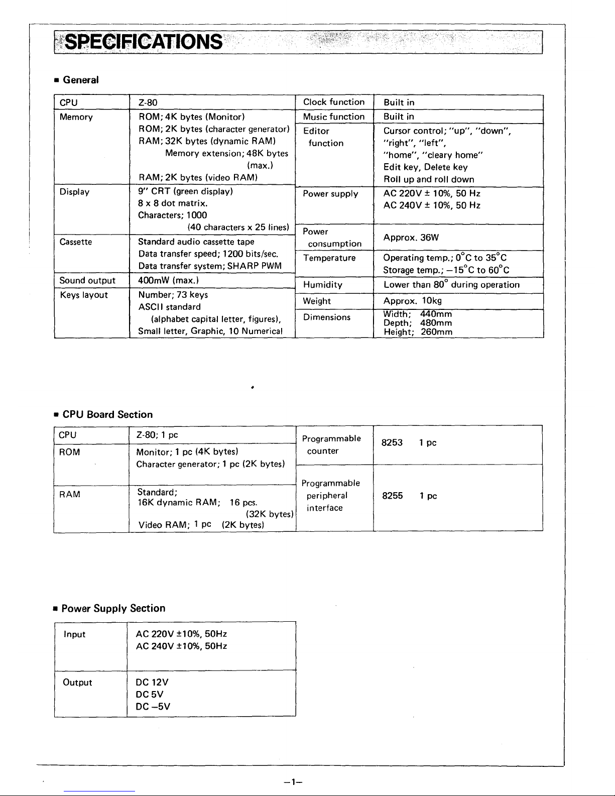
I
• General
CPU
Z-80
Clock
function
Built in
Memory
ROM; 4K bytes (Monitor) Music
function
Built
in
ROM; 2K bytes (character generator)
Editor
Cursor
control;
"up",
"down",
RAM; 32K bytes (dynamic
RAM)
function
"right",
"left",
Memory extension; 48K bytes
"home",
"cleary
home"
(max.)
Edit
key, Delete key
RAM; 2K bytes (video RAM)
Roll
up
and
roll
down
Display
9"
CRT (green display)
Power supply
AC
220V
± 10%,
50
Hz
8 x 8
dot
matrix.
AC
240V ± 10%,50
Hz
Characters;
1000
(40 characters x
25
lines)
Power
Cassette
Standard
audio
cassette tape
consumption
Approx.36W
Data transfer speed;
1200
bits/sec.
Temperature
Operating
temp.;
O°C
to
35°C
Data transfer system; SHARP
PWM
Storage
temp.;
_15°C
to
60°C
Sound
output
400mW (max.)
Humidity Lower
than
80° during operation
Keys layout Number;
73
keys
Weight
Approx. 10kg
ASCII
standard
Width;
440mm
(alphabet capital letter, figures),
Dimensions
Depth;
480mm
Small letter, Graphic, 10 Numerical
Height;
260mm
•
CPU
Board Section
CPU
Z·80; 1 pc
Programmable
8253
1
pc
ROM
Monitor; 1 pc (4K bytes)
counter
Character generator; 1 pc
(2K
bytes)
Programmable
RAM
Standard;
peripheral
8255
1 pc
16K
dynamic
RAM; 16 pcs.
interface
(32K bytes)
Video RAM; 1 pc
(2K
bytes)
• Power
Supply
Section
Input
AC 220V ±10%, 50Hz
AC
240V ±10%,
50Hz
Output
DC12V
DC5V
DC-5V
-1-
Page 4
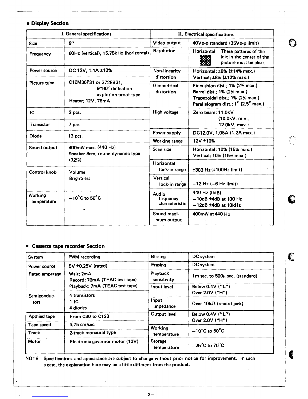
• Display Section
I. General specifications
11.
Electrical specifications
Size
9"
Video
output
4OVp-p standard (35Vp-p limit)
Frequency
60Hz (vertical), 15.7SkHz (horizontal)
Resolution
Horizontal
These patterns
of
the
11
left
in
the
center
ofthe
picture must be clear.
Power
source
DC
12V,
1.lA
±10%
Non-linearity
Horizontal;
±8%
(±14% max.)
distortion
Vertical;
±8%
(±12% max.)
Picture tube
Cl0M36P31
or
2728B31;
Geometrical Pincushion dist.;
1%
(2%
max.)
9"90°
deflection
explosion proof type
distortion Barrel dist.; 1
%
(2%
max.)
Trapezoidal dist.;
1%
(2%
max.)
Heater; 12V. 7SmA
Parallelogram dist.; 10 (2.So max.)
IC
2 pes.
High
voltage
Zero beam; 11.0kV
(10.0kV, min.,
Transistor 7 pes.
12.0kV, max.)
Diode 13 pes.
Power supply
DC12.0V, 1.0SA (1.2A max.)
Working range
12V ±10%
Sound
output
400mW max. (440
Hz)
Scan size Horizontal; 10% (lS% max.)
Speaker
Bem,
round dynamic type
Vertical; 10% (lS% max.)
(320)
Horizontal
Control knob Volume
lock-in range
±300
Hz
(±100Hz limit)
Brightness
Vertical
lock-in
raniJe
-12
Hz
(-6
Hz
limit)
Working
Audio
440
Hz
(OdB)
-10°C
to
SOOC
friquency
-lOdB
±4dB
at
100
Hz
temperature
characteristic
-12dB
±4dB
at
10kHz
.
Sound maxi-
400mW
at
440
Hz
mum
output
• Cassette tape recorder Section
System
PWM
recording
Biasing
DC
system
Power source
SV
±0.25V (rated)
Erasing
DC
system
Rated amperage
Wait; 2mA
Playback
1 m sec.
to
SOO/-l
sec. (standard)
Record;
70mA (TEAC test tape)
sensitivity
Playback; 7mA (TEAC test tape)
Input level
Below 0.4V
("l")
Semiconduc·
4 transistors
Over 2.0V ("H")
tors
1
IC
Input
Over
10kll
(record jack)
4 diodes
impedance
Applied tape
From C30
to
C120
Output
level
Below
O.4V
("l")
Over 2.0V
("H")
Tape speed
4.7S cm/sec.
Working
-10°C
to
SOoC
Track
2-track monaural
type
temperature
Motor Electronic governor motor (12V)
Storage
-2SoC
to
70°C
temperature
NOTE
Specifications and appearance are subject
to
change
without
prior notice for improvement.
In
such
a case,
the
explanation here may be a little different from
the
product.
-2-
Page 5
The machine comprises five main units, CPU board, display, cassette
tape
recorder,
keyboard,
and power supply
circuits. For a quick solution
to
most
operating difficulties, first
consult
the
chart
below
to
find which section
of
the
machine
is
subjected
to
the
trouble, and
next
to
do
the
checkings according
to
more
detailed instructions given
in
the succeeding pages.
Start
Switch
on
Yes
Yes
I
s
the
cassette
~ecorder
normal?
Yes
Yes
Yes
End
No
No
No
No
No
-3-
Check
for
the
power
supply
circuit.
Check for
the
CRT
display.
Check
for
the
cassette
recorder.
Check
for
the
keyboard.
Check
for
the
CPU
board.
Page 6
CPU BOARD SECTION
The CPU
board
is
composed
of
the
following six blocks. When it
gets
in
trouble,
first
locate
which
block
is
concerned
with
the
trouble,
and
next
try
to
check
for its
corresponding
circuits;
the
wiring
diagrams
of
every block
will be
shown
separately.
CPU
in
trouble
Display
block
No
Cassette
recorder
block
Keyboard
block
Audio
block
Clock
block
No
Gets
in
trouble
instantly
with
power
on.
No
Yes
Yes
Yes
Yes
Yes
Yes
•
Checking-methods
of
each
circuit
Check
for
video
RAM
circuit.
Check
for
IC50
(8255)
and
its
peripheral
parts.
Check
for
IC50
(8255)
and
its
peripheral
parts.
Check
for
IC47
(8253)
and
its
peripheral
parts.
Check
for
IC47
(8253)
and
its
peripheral
parts.
Memory
circuit,
Reset
circuit
and
its
peripheral
parts.
1.
By
touching
IC
insulating parts by fingers:
'.:
If
they seem
too
hot
by heat generation;
IQ.oi~"j:fefl~ctive'-IC
load
-4-
~r(~':'\
V
;~:~.'~,
'l.~/
Page 7
/
• Display Block
DO
-
Bus
driver
07
-
~
-'--
--
WR-
RD
CSD
~
/
AO
I
)
A9
Who
le reversal
1.
Sync. signal
is
not
produced.
2.
Video signal
is
not
produced.
3.
Irregular display
characters
4.
The display
is
positionally
deviated.
5.
Position
is
correct
but
characters are abnormal.
Character
h
:>
Video
signal
generator
~
Shift
register
<~/:.
L
)
BLNK
).
Sync.
signal
-
I
Video
'\/'
RAM
L--
1"1
Display
~
Oscillator
V
controller
circuit
Address
selector
~
C~D
T
Block
Diagram
of
Parts
around
Video
RAM
Vertical sync. signal: Check
for
pin @
of
IC20.
Horizontal
sync. signal: Check
for
pin00f
IC20.
Is
V·GATE
signal
for
pin @
of
IC2 high level?
Yes; IC2
No;
IC50
Is
V-BLANK
signal present at pin ®
of
IC20?
Yes; IC20
No;
IC2
Is
H-BLANK
signal present at pin
CD
of
IC20?
Yes; IC20, IC31
No;
IC2
Does pin ®
of
IC8 develop video signal?
Yes; IC8
No;
IC2, IC10, IC4
Check IC14,
1<;:20.
Check IC21, IC22, IC26, IC27, IC32,
IC33
Check IC15 and IC16.
-5-
Page 8
•
Cassette
recorder/Keyboard Block
PC1
D7
-\
PC5
PC4
PC3
-I
LO
In
'"
~
DO
Q)
u
-
~
e
RD
c
WR
-
~
Q)
.r:
PA3
Q.
-
.;:
~
Q)
"-
Q)
:0
cs
co
PAO
E
-
E
~
Al
Cl
PB7
e
-
0-
)
-
AO
RESET
PBO
r
...h
r
J,
I
1
l
I I
t-'
1)
L
Motor
controller
I"
I
I
Decoder
I
1,
I
~
I
I
I
J,
L
-------,
WRITE
READ
SENSE
I
I
I
I
I
Cassette
I
I
I
MOTOR
I
______
-.1
------1
9
~
o
I
I
I
I
I
I
I
I
Keyboard
H I
) i
A :
_______
J
Block
diagram
of
Parts
around
Cassette
recorder/Keyboard.
1.
"LOAD"
operation
is
impossible.
2.
"SAVE"
operation
is
impossible.
3.
Motor
doesn't rotate.
4.
Motor
doesn't stop.
5.
Key
input
is
ineffective.
Is
output
signal present at pin Q)
of
IC10?
Yes; IC50
No;
IC10
Is
output
signal present at pin @
of
IC50?
Yes;
ICl
0
No;
IC50
Is
voltage at pin ®
of
IC39 at
"Iow"
level?
Yes;
IC4,
01
No;
IC39, IC5
Is
voltage at pin ®
of
IC39 at
"high"
level?
Yes;
IC4,
01
No;
IC39, IC5
Check
for
IC52 and IC50.
Page 9
•
Audio/Clock
Block
RD
----;
WR---i
Programmable
counter
(8253)
"-
--------------
~-'"
------------
-------.--------~---
31.5KHz
")
_
~
Clock
function
INT
J
1/2
frequency
division
I-------C>
Audio
output
CS
----;
A1
------1
1-----<
2MHz
AO---L
____
~
WR----1
CS
------1
RD-----4
Latch
Oscillator
circuit
for
Tempo
L--,-
_____
..4
DO
Block Diagram
of
Parts
around
Audio/Clock
Block
1.
Abnormal sound
output
2.
Clock
function
is
abn·ormal.
--r,.,..,,
__________
..
___
---------
Is
output
signal present
at
pin
@
of
IC47?
Yes; IC45, IC48
No;
1C47, IC51
Is
31.5KHz
signal
input
to
pin @
of
IC47?
Yes; 1C47 (8253) and surrounding are
faulty.
No; IC20 (Check
if
8MHz
signal
is
supplied
to
pin @
of
IC20)
-7-
Page 10
~-~-~----~
~~--~---~---~
•
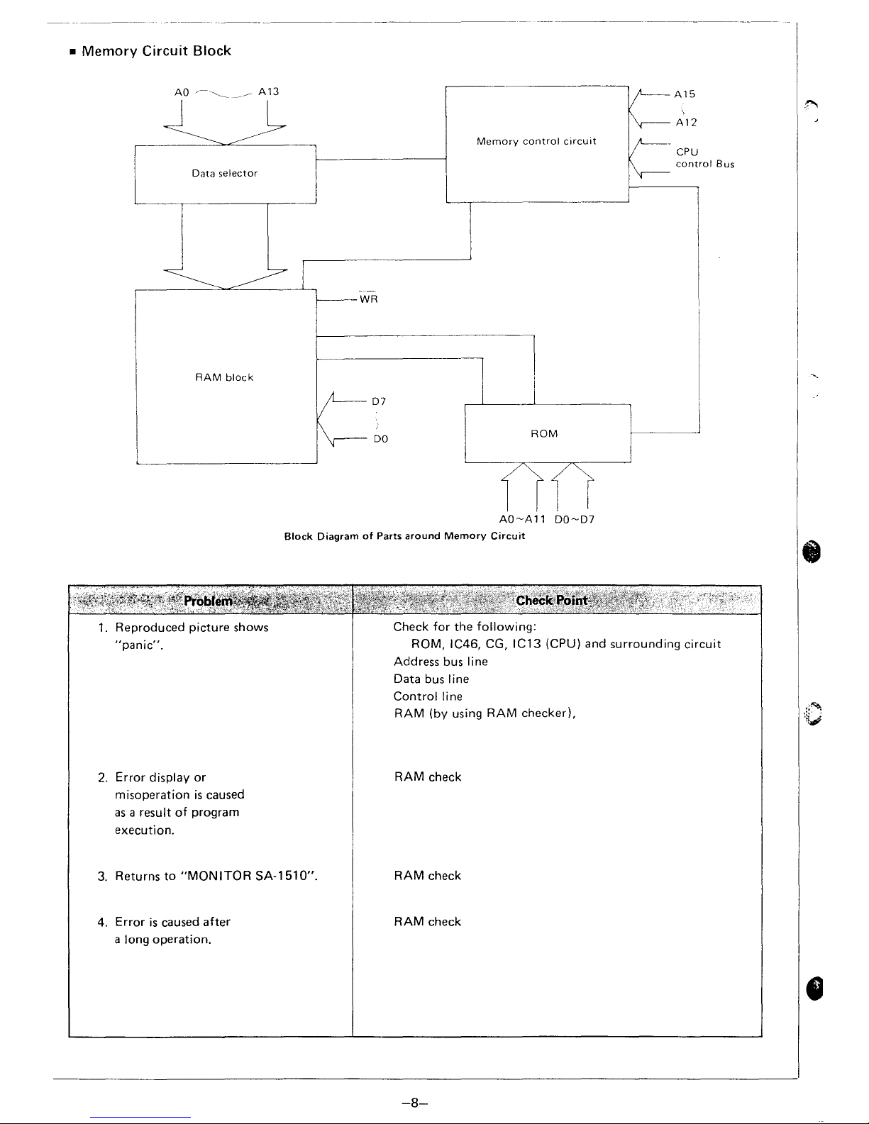
Memory
Circuit
Block
Data
selector
WR
RAM
block
07
DO
Memory
control
circuit
ROM
A15
\
A12
CPU
control
Bus
AO~All
DO~D7
Block
Diagram
of
Parts
around
Memory
Circuit
1.
Reproduced picture shows
"panic".
2.
Error display
or
misoperation
is
caused
as
a result
of
program
execution.
3.
Returns
to
"MONITOR
SA-1510".
4. Error
is
caused
after
a long operation.
Check
for
the
following:
ROM, IC46, CG,
IC13
(CPU) and surrounding
circuit
Address bus line
Data bus line
Control
line
RAM
(by using
RAM
checker),
RAM
check
RAM
check
RAM
check
~8~
Page 11
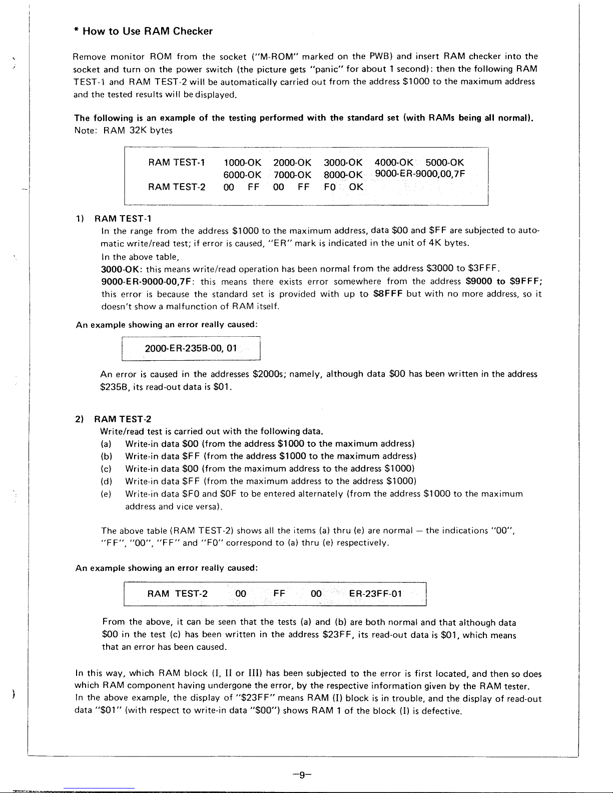
*
How
to
Use
RAM
Checker
Remove
monitor
ROM from
the
socket
("M-ROM"
marked
on
the
PWB)
and
insert
RAM
checker
into
the
socket
and
turn
on
the
power
switch (the
picture
gets
"panic"
for
about 1 second):
then
the
following
RAM
TEST-l
and
RAM TEST-2 will be
automatically
carried
out
from
the
address
$1000
to
the
maximum address
and
the
tested
results
wi
11
be displayed_
The following
is
an
example
of
the
testing
performed
with
the
standard
set
(with RAMs being all normal).
Note: RAM 32K
bytes
RAM
TEST-l
RAM
TEST-2
1) RAM
TEST-l
1000-0K
6000-0K
00
FF
2000-0K
700o-0K
00
FF
3000-0K
800o-0K
FO
OK
4000-0K
5000-0K
9000-ER-9000,00,7F
In
the
range from
the
address
$1000
to
the
maximum
address,
data
$00
and
$FF
are subjected
to
auto-
matic
write/read
test;
if
error
is
caused,
"ER"
mark
is
indicated in
the
unit
of
4K
bytes_
In
the
above table,
3000-0K:
this
means
write/read
operation
has been normal
from
the
address
$3000
to
$3F F F_
9000-ER-9000-00,7F:
this
means
there
exists
error
somewhere
from
the
address
$9000
to
$9FFF;
this
error
is
because
the
standard
set
is
provided
with
up
to
$8FFF
but
with
no
more address, so it
doesn't
show a malfunction
of
RAM
itself.
An
example
showing an
error
really caused:
200Q-E R-235B-00, 01
An
error
is
caused in
the
addresses
$2000s;
namely,
although
data
$00
has been
written
in
the
address
$235B,
its
read-out
data
is
$01.
2) RAM TEST-2
Write/read
test
is
carried
out
with
the
following
data.
(a) Write-in
data
$00
(from
the
address
$1000
to
the
maximum
address)
(b) Write-in
data
$F
F (from
the
address
$1000
to
the
maximum
address)
(c) Write-in
data
$00
(from
the
maximum
address
to
the
address
$1000)
(d) Write-in
data
$FF
(from
the
maximum
address
to
the
address
$1000)
(e) Write-in
data
$FO and
$OF
to
be
entered
alternately
(from
the
address
$1000
to
the
maximum
address
and
vice versa).
The above
table
(RAM TEST-2) shows
all
the
items (a)
thru
(e) are normal -
the
indications
"00",
"FF",
"00",
"FF"
and
"FO"
correspond
to
(a)
thru
(e) respectively.
An
example
showing an
error
really caused:
RAM
TEST-2
00
FF
00
ER-23FF-Ol
From
the
above, it can be seen
that
the
tests (a)
and
(b) are
both
normal
and
that
although
data
$00
in
the
test
(c) has been
written
in
the
address
$23F
F, its
read-out
data
is
$01,
which means
that
an
error
has been caused.
In
this way, which RAM
block
(I,
II
or
Ill)
has been
subjected
to
the
error
is
first
located,
and
then
so does
which RAM
component
having undergone
the
error,
by
the
respective
information
given by
the
RAM tester.
In
the
above example,
the
display
of
"$23FF"
means
RAM
(I)
block
is
in
trouble,
and
the
display
of
read-out
data
"$01"
(with respect
to
write-in
data
"$00")
shows RAM 1
of
the
block
(I)
is
defective.
-9-
Page 12
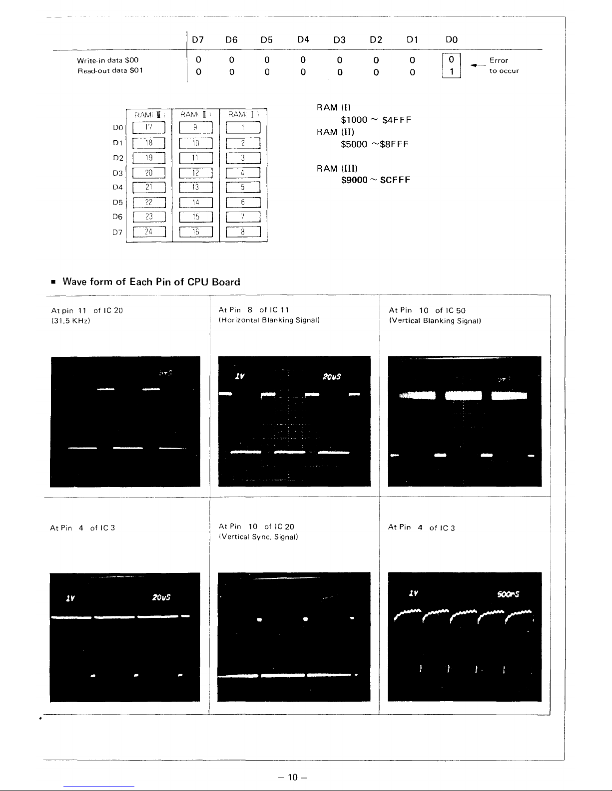
Write-in
data
$00
Read-out
data
$01
f~AM
1II.
00
01
02
03
04
05
06
07
I
I
I
I
I
I
I
I
17
I
18
I
19
I
20
I
21
I
22
I
23
I
24
I
07
06
0
0
0
0
RAM n '
RAM
I
9
I I
1
I
10
I
I
2
I
11
I
I
3
I
12
I
4
I
13
I
5
I
14
I
6
I
15
I
7
I
16
I
8
I)
I
I
I
I
I
I
I
I
-~-----~"-.~
~
-----~-
~----------
-" -_._-----
05
04
0 0
0 0
03
02
01
0
0
0
0
0
0
RAM
(I)
$1000 ~ $4FFF
RAM
(Il)
$5000
~$8FFF
RAM
(Ill)
$9000 ~ $CFFF
00
IT]
Error
--
to
occur
• Wave
form
of
Each
Pin
of CPU
Board
-------
---------~~
------~----~------------.----------------.
At
pin
11
of
le
20
(31.5
KHz)
At
Pin 4
of
le
3
At
Pin 8
of
le
11
(Horizontal
Blanking
Signal)
At
Pin
10
of
le
50
(Vertical
Blanking
Signal)
.~---~-----+----------------+---------------1
At
Pin
10
of
le
20
(Vertical
Sync.
Signal)
-
10-
At
Pin 4 of
le
3
Page 13
Write-in
d3tJ
$00
Fiead-out
data
$01
DO
01
0:)
D3
04
0
,-
,)
D6
D7
"'\iv1
ill
I
1'1
I
I
IR
I
I
1 q
I
I
?ll
I
I
:'1
I
I
??
I
L)I
I
I
I',;
]
L--
I
I
07
o
o
f
-<
~'\
~\J'I
"
1 C
TI
I
I
I
11
I
I
1?
I
I
n_~
I
1
~
I
I
I'
I
L"
I
06
o
o
"t\;\
1
I
1
I
2
I
\
I
,I
I
s
I
tl
I
I
j
I
I
I
I
I
I
I
I
I
05
o
o
04
o
o
03
02
01
o
o
RAM(l)
o
o
o
o
$1000 ~ $4FFF
RAM (Il)
$5000
~$8FFF
RAM
(Ill)
$9000 ~ $CFFF
DO
Error
--
to
occur
•
Wave
form
of
Each Pin
of
CPU Board
At
pin
11
of
IC
21)
(31,5
KH,)
At
Pin
-4
of
IC 3
- T
!
At
Pin 8 of
IC
11
(Horizontal
Blanking
Signal)
AtPin
10
oflC20
(Vertical
Sync,
Signal)
---------
----,---
------
-
----------
-----------l
I
At
Pin
10
of
IC
50
(Vertical
Blanking
Signal)
At
Pin 4 of
le
3
_________
-1-
_______________
--'--
______________
----'
-10-
Page 14
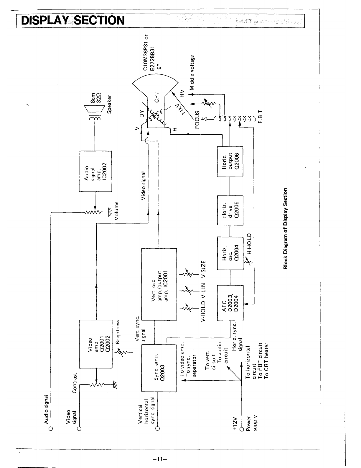
....
I
Audio
signal
Video
signal Contrast
Vertical
horizontal
sync. signal
+12V
Power
supply
Video
amp.
02001
02002
t
Beightoe"
Vert. sync.
signal
,-------------
Sync. amp.
02003
To video amp.
To sync.
separator
To
vert.
circuit
To audio
circuit
Horiz. sync.
signal
To
horizontal
circuit
To
FBT
circuit
To CRT heater
Vert.osc.
amp'/output
amp. IC2001
ttt
V-HOLD
V-LlN
V-SIZE
AFC
H
Horiz.
02003,
osc.
02004
02004
~
H-HOLO
Volume
Horiz.
drive
02005
Audio
signal
amp.
IC2002
Video signal
Horiz.
output
02006
Block Diagram
of
Display Section
)
I----~IIO
~~~
Speaker
Cl0M36P31
or
E2728B31
9"
'\'+-
HV
H~
'\
• • Middle voltage
FOCUS
F.B.T
c
-
(J)
-C
~
~
en
~
-I
-
o
z
Page 15
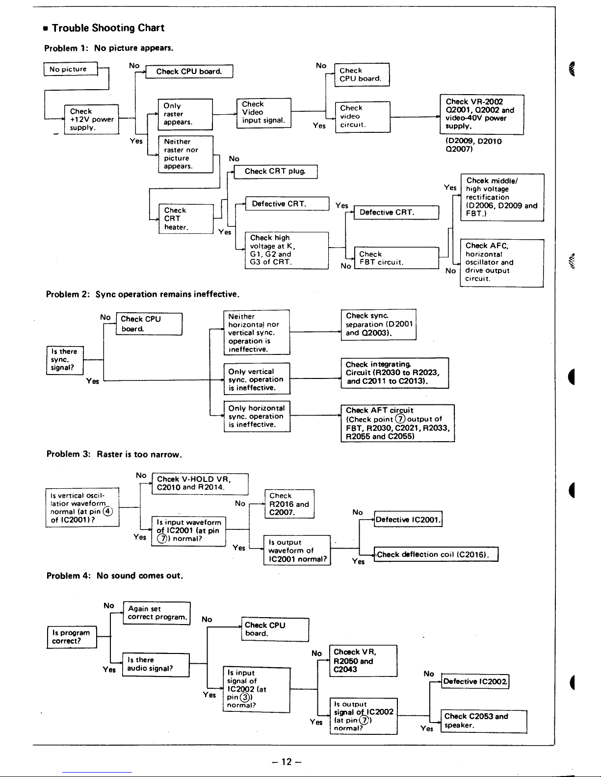
• Trouble Shooting Chart
Problem 1: No picture appears.
[
No
picture
1
Nri
Check CPU board.
I
NOl Check
I
CPU board.
Only
H Check
Check
VR-2002
YChKk
Video
Check
02001.02002
and
r
raster
+12V
power
~
input
signal.
-
video
vide0-40V
power
supply.
appears.
Yes
circuit.
supply.
- -
Yes
Neither
(02009.
02010
L..>
raster
nor
02007)
picture
No
appears.
rl
Check
CRT
plug.
I
Chcek
middle!
Yes
high voltage
J
--.j
Defective CRT.
r
rectification
Check
Yes
(02006,02009
and
ri Defective
CRT.
FBT.)
L..."
CRT
heater.
Yes
~-
Check high
voltage at
K,
r---
Check
AFC,
~
G1,
G2
and
~.
Check
horizontal
G3
of
CRT.
No
FBT
circuit.
oscillator
and
No
drive
output
circuit.
Problem 2:
Sync
operation remains ineffective.
NH
Check CPU
I
Neither
Check sync.
board.
r-"
horizontal
nor
separation
(02001
vertical sync.
and
020031.
operation is
llsthere
r
ineffective.
sync.
Check integrating.
signal?
Only
vertical
Circuit
(R2030
to
R2023.
Yes
sync.
operation
and C2011
to
C2013).
is ineffective.
Only
horizontal
Check
AFT
circuit
--10
sync. operation
(Check
point
(j)
output
of
is
ineffective.
FBT.
R2030.
C2021.
R2033.
R2055
and
C2055)
Problem 3: Raster
is
too
narrow.
N~
Chcek
V-HOLD
VR,
I Check
C2010
and
R2014.
Is vertical asci I·
latior
waveform
f----
No
~
R2016
and I
normal (at
pin
@)
C2007.
NrlDefective
IC2001.j
of
IC2001)?
Is
input
waveform
......
of
IC2001
(at
pin
-
Yes
(7))
normal?
Is
output
Yes
...........
waveform
of
IC2001 normal?
r--Y'Check
deflection
coil
(C20161.
Yes
I
Problem 4: No sound comes
out.
Again set
correct
program.
Is
there
audio
signal?
.-----.ot
Check CPU
board.
Yes
Is
input
signal
of
IC2002
(at
pin@)
normal?
-12
-
No
Yes
Chceck
VR.
R2050and
C2043
Is
output
si{Jlal
~~C2002
1---1
(at
pinl,J,)
normal?
Defective IC2002.
Check
C2053
and
speaker.
Page 16

--.-
.-
•..
_---
.~
-._._._._------_.-
..
-------~---
-~~-.-----
•
Waveforms
of
Display
Section
Video
input
signal
Video
output
signal
Video
output
signal
CD
ell
CID
+[1111[[
Jl
·+llllilll
I111111
'+~I~~~
'
..
_-
~111I~1
5ms
5ms
5ms
Sync.
input
signal
Sync.
signal
amp.
output
Vertical
sync. signa;
@
@
®
Tuu
T'l
~'-
fr-
1
r
12r
~
1V
..
-
20l"s
20l"s
2ms
Vertical
oscillator
Circuit
Vertical
output
waveform
Vertical
drive
collector
waveform
1;
@
.:l
u~
Tn
l
T
'O]LJ
IV
~
'if
t
ov
5ms
1.SV
5ms
Voltage
at
pin ® of
RH·IXOO15
Vertical
deflection
coil
voltage
waveform
Vertical
linearity
circuit
waveform
l])
ID
ltJl
-f
~
"""1\
~
/'
~
1.5Vpp
1.5Vpp
8Vpp
L I
~
t
lJ
~J
5ms
5ms
Sms
Horizontal
sync. SIgnal
waveform
AFC
waveform
FBT
waveform
@
1])
.1])
·ffl
n
1-
l
T.~
4V
7V
'LJ
I
5V
,
.-
20l"s
201l
201"5
-13-
Page 17

Horizontal
oscillator
waveform
1ll
5V
lit
OV
20~s
Horizontal
drive
collector
waveform
@'
15Vpp
1
20~s
AFC
pulse
@
T
160V
20~s
Audio
input
signal
Horizontal
oscillator
emitter
waveform
Horizontal
oscillator
output
waveform
\tT,
20
{(j.
~
5V
'"
OV
20~s
2O~s
Horizontal
output
base
waveform
Horizontal
output
pulse
5V
lM
®
20~
20~s
Middle
voltage
FBT
pulse
Video
power
supply
pulse
-----------~--------~----~~--------J
2O~s
Audio
output
waveform
-14-
ov
2O~s
The figures encircled
by
0
in
the
above
refer
to
those
of
"Wiring Diagram"
---
"Check Points
of
Waveforms".
Page 18

JLJ1Jl_
I
....
(J1
I
JlJlJL
Play
button
Power
supply
o-o0~
for
motor
~
G
0
WRITE
READ
:
I
Erase head
c
~
I
'--
..
•
Record/playback
head
Differentia-
tion
circuit
R3005
C3002,R3005
Amplifier
circuit
I
03001,03002
+5
v
-
Amp.
circuit
03003
Amp.
circuit
Limiter
circuit
IC3001
(1/2)
Block Diagram
of
Cassette Tape Recorder
TAPE
~
en
en
m
-t
-t
m
~
):>
'"tJ
m
::D
m
o
o
::D
c
m
::D
(f)
m
o
....
6
z
""
{~\
'g:
t{:
(;:
!~
"''*'"
.C~
~r..,:
§
-0.
~
ill..
Page 19

• Trouble Shooting Chart
Problem 1: Even if
the
play
button
is
pushed, neither motor
rotales nor tape moves.
Yr-1
Electronic
governor J
motor
defective.
Check
for
motor'
voltage:
see
Nri
Switch
defective J
if
there
is
+12V
t--
between
M+
and
M-.
Is voltage
at
the
switch
N~
(inter·
locked
with
the
I--
play
button)
in
high level?
Check
for
vOlt(!)
at
cheak
point
4
--<
(SENSE):
it
must
be
Yes
OV
with
switch
on and
+5V
with
switch
off.
Problem 2: Record (SAVE) operation
of
program
is
impossible.
N;1
Switch defective.
See
if
the switch SW3001
No
surely gets
in
action
1 Check
for
CPU board. I
when the record
button
I-
is
pushed.
+5V
must be
Yes
r-<
f----
No
Does there
come
present
at
check
point
N~
SW3001 defective:
@.
any signal
tr®
r-
Yes
check
point
6 ?
Is
there
any
check
for
R3002.
'-i
signal present
I--
Yes
at
the
base
of
03001.
Is there any signal
present
at
the
Yes
record/playback
head.
Problem 3: Playback (LOAD)
of
program
is
impossible,
or
error
is
caused.
Ye.:.! Make
su~e,of
the
tape-'
I 1 start POSition.
r-------~
r---------------~
Does normal
waveform
arise
at
pin
@?
No
Check
for
power
supply
+5V
of
CPU
board.
And
check
for
plug
and
cable
(6
pins).
H
Check
for
power
l--
No
supply
+5V.
I
No
Check
for
IC3001,
r-
each resistor and
SW3001.
The waveform
is
not
normal
with
much
nOises,
or
no
waveform develops.
U Check
for
1_
Yes 1 each voltage. I .
Check
for
+12V
power
supply
circuit
(for
motor
in
tape recorderl and CPU
board.
Check
for
+5V
input
voltage I
and
R3024.
Y11
Record/PlaYbackl
head defective.
f--
Poor
contact
of
SW3001.
Check
for
Q3001 and
Q3002
.
.....
Is voltage applied
to
the
No
erase
head?
Yes Doesn't
the
erase
.--
head operate because
of
SW3001
in
trouble?
output
voltage
waveform
~
Check
for
the
size
of
~
Yes
of
Q3003.
Much
noise
-16
-
Check
for
around
Q3003.
---..
Azimuth
adjustment
The voltage
of
the
record/playback
head
is
too
low.
is
improper.
Page 20

•
Waveforms
of
Cassette
Tape
Recorder
1st stage amp.
output
waveform
CD
~
\Ni'
(
'~
Lp
1
Operational amp. input waveform
@
Tt
1'1
f1
1.SVpp
~v
"
V V
v
v
~
_w.
Record input waveform
(J)
Te-
e-
-
r-
1.SVpp
1
L-
-
Head
input waveform
®
T~
i\~
\\
6Vpp
I1
/ V V
Operational amp. input waveform
Operational amp. input waveform
@
@
L
6mv~
pp
1.SV
T
OV
Operational amp.
output
waveform
Output
waveform
@
@
T
T
4Vpp
5Vpp
I
~
---.L
Record amp. waveform
Record amp. waveform
@
®
l~
r-
e-
e-
r-
T
-
e-
4.SVpp
PP)
1
~
~-
'-
"-
The figures encircled
bvOcorrespond
to
those
of
"Wiring Diagram" - "Check Points
of
Waveforms".
-17-
Page 21

• Azimuth Adjustment and Head Cleaning
* Azimuth adjustment
of
record/playback head
1.
Connect a synchroscope
to
the
collector
of
03003.
2.
Load a test tape (TEAC, 3kHz-signal recorded) and play
it
back.
3. Rotate the azimuth adjusting screw so
that
the waveform on a synchroscope will be
the
maximum.
Record/playback
head
Head cleaning
Head
azimuth
adjusting screw
Clean
the
heads, capstan and pinch roller often,
to
remove
dust
and tape residue. Foreign material
on
them
impairs the sound
quality
of
both
recording and playback.
Open the cassette holder, remove
the
tape, push
the
play
button
and clean
them
with a
soft
cloth moistened
in
alcohol.
Erase protection
To protect a cassette tape from being
accidentally erased it was designed with
two
removable tabs.lWhen
the
tabs
are removed, it
is
impossible
to
push
the
record
button.
When no cassette
is
inside
the
machine, no pushing
of
the
record
button
is
allowed, either. Nevertheless, pushing
the
button
strongly may cause a trouble.
Pinch roller
!
, Capstan
-18
-
Page 22

------------
.. -..
-
...
~----------------------------------------,
0----
Rectifying
and
ACINPUT
Smoothing
Circuit
o-~~-
Q;
E
~
c
Rectifying
and
co
t!:
Smoothing
Circuit
Block Diagram
of
Power Supply Section
• Waveforms
of
Each
Parts
Waveform
of
pin
®
Waveform
of
pin(jJ)of
IC401
0401
collector
waveform
of
IC301
and
IC401
vf\/\
11:Jl1
v
illIL
~~
f---451l5~
45115
Waveform
of
pin(lj;of
IC301
0301
collector
waveform
--------------------
------
I
IlJlf
f[lJL
~q
p~
45115
45J.L5
-19-
+12V
G
+5V
G
-5V
G
Page 23

• Trouble Shooting Chart
Problem 1:
No
voltage appears
at
any
output
terminal.
Check primary circuit which includes
the
transformer.
Problem 2:
-5V
is
not
developed.
Is
there
AC
9V
present across
the orange
lead?
Check
for
T101.
Is
there DC
10V
present across C201?
Problem 3: +12V
is
not
developed.
Is there
AC
20V
present across
C401
Check
for
FR201,
0201,
C201 and C202.
Is
there
DC-5V
present across C203?
No
No Check
for
0401,
C402,
C403
and R401.
Is
there DC
23V
present across C402?
Problem 4:
+5V
is
not
developed.
Check
for
T1 01.
Is
the waveform
at
col·
lector
of
0401
normal?
No
Check
for
IC201, R201,
C203
and C204.
Check
for
L201 and
Yes
F202.
Check
for
IC401 and
its
peripheral parts.
Check
for
0401
and
0402.
Leave
R403
be open;
does there appear
0.3VI3=P
pulse
at
pin
QJl
of
1C401?
Check
for
L401, C405
and C409.
Check
for
IC301 and
its
peripheral parts.
Is
there AC
13V
present across
C301
?
No
Check
for
0301,
C302, C303
and F301.
Check
for
0301
and
0302
switching circuit.
Is
there DC
15V
present across C302?
Is
the
waveform
at
col·
Yes
lector
of
0301
normal?
-20-
No
Leave
R303
be open:
does there appear
O,a.
Vp-p
pulse
at
pin
<U
of
1C301?
Check
for
L301, C305
and C309.
Page 24

1
2
3
4
5
7
:,
.;;-'
8
9
10
)
11
A
B
C
D
E F
G
H
,
•.
CIRGtJl-r~'DI~GRAM
.AND PRINTED
..
WII;~INGi:iBOARD
I
Notes:
The
circuit
diagram
and
printed
wiring
board
subject
to
change
without
prior
notice
.
• CPU Board Circuits (1)
..
•
.. .. .. ..
_ 0
...
.. ..
..
..
..
_ 0
...
.. c ..
...
..
..
...
o
000
000
0
.
J
,
•
~
·
~
•
N ,
·
~
,
~
•
=
~
-
,
~
•
,
..,
:~
.,~
:~
",:1
.
"'~
0
-
-'"
uV>
uV>
uV>
_.J
~
:>--
_.J
~>=-
_.J
. .
=
.
,
.
~
·
~
N
-
.
~ · ~
.
~
N
.
.
,
"
~
.
~
,
.
"
.
~
N
-
~
~ ~ ~
·
~
0;
~
~
e
. , .
N
~
.
•
,
::
,
~
: :
~
:
:
: :
:
;;
~
~
~
~
~
~
~
0
g
U
.
",0
I~
:
-.,
u'
_N
I~
li
.
I:
I~
I~
I~
'i
,;
I~
I~
li
I~
,
0
>
"
~
~
~
"
~l
~
~
~
"
&
•
=!
~L
.~
~~
I;
~~
~~~
N
•
~
·
,
"
..,
....
~
:n
to
~~
~:
uV>
_.J
,
~
-
~I
"I
"I
'I
'I
'\
"I
to
~~
N
~
I:
I~
I~
I.
I;
I~
I~
li
I~
"
!~
li
f.
>
li
J
.
J
:
~
~.
'"
0
~
.,
..
.,..,
"~,,
~-.!
::
"'
....
~I=-
,--
f
"'
....
d~
~~ ~~
uV>
uV>
.....
~!
_.J
_.J
~ t =~
'#)
f::l
~:
0
3
o
~
~
1
~~
o.
I.
NO
I:
~~
I~
I;
,
-
::
=
.~
~
~
~
~g
'=~
1=
I§
lE
~
~~
J J J
.
"
0
.
~~f.,
~
0
·
0
·
"
I~
..
'"
~Q
....
~~
....
-'"
..
..
uV>
uV>
~
_.J
---'
~~
0 u
·
.
0 u
·
.
0'g
uO
"
'1
't
°1
"
'1
'~
°1
~
·
I~>-
o~3
J
J
rJ
I~
I~
I;
I~
at
...
""""
J J J J
f_U
..
~N
·
~
.
~
0
;;
~
~
N
>
~
=
: :
:
~!r
..
'"
°
.0
~~
~
"'~
..
uo
u"
uV>
~
_
....
_.J
~
.~!
~.
.
,
~
=
~
.
:!!
:
~
·
·
&
~
~
-
! ! !
..
"J
1
·
.~
'1
;;
~
.'
1 1
~1
~1 1 ~1
f
.;~
....
-
.0
r--
NN
I~
i
I~
li
.
~
I~
~~
~
:2
.2
=
·
-
21
-
~
'8
~'1
tt
=
0
!!oS
~~
. .
I.
I~
I~
I~
j~
I~
I~
J
.1
J J
~
~
~
~
.
!
~
.
"1
01
"1
'1
,
~
,
•
.
.
~
I~
"1
~
I~
!!
Is
<t
o
co
,
N
::2:
E
.£:
0
~
M
cv;
.£:
Cl
::l
0
....
.£:
.....
Q)
C
>
L!)
+
0
.....
C.
::l
'1:l
~
"S
a...
-
J:
Page 25

N
N
I
....
...
,-
'"-
.Ji-
. ,
Icn
LS74
f-
a.
.1
..
f-~
-
IC'
':CN)
"o.
....
~
;
....
,,~,
•
IQ
~
c,
"'"
..
IM
t~OI'
~~~~t>~~~~;'
~L,~
...
~
.z.____
~~
•.
..
.,
LIDO
ICI6
LSZ411
it
ItliI
t'.:
..
.-
WI
'"'-
.r-
m
...
e
..
,
...
._o\!
n
.v
" I
Oe
0.
o.
or.
0.
Or
ICI5
2016
B
110
AI
AI A
.......
•.
c --HI, ...
i
.....
".
"
r".--t------'~·,
...
....
....
,
........
cD
..........
,'"'0"
A,A,
..
.
(H): Pulled up
to
+5V line through 3.3K ohm.
--
.-
.-
'Ic,,"
121:
O~It'
...............
~
~
'I'
Mlvl
Z
l41C~
!C20
"B14298
"
r-r
'H'
..
"
~..
.~
-
..
~
I •
e
..
.--
--to
svIlllCNI"IIO'----------------'
Ir.
......
-~
-.......".
'co,
....
l
......
~
~
....,
fm
_1~_vI
.•
,;:-to
.....
'"""
~Y.iiitiii
=lt
1_"IY'
'"
'lOO
."
,-
.'I.
.......
.v-r~
MiUii>--.l
I"
C~QM)
I~
D'
- I"
..
"
IN
I"
I"'
1",
,.n
"'71
A,
>---'I'D
.,
>---lII'D
:~
::
A.
'
••
R1t
11
CLOQ(
iiiiIt
I
Q.D
.n
try
cl
--
r
..
Bd
A•
'.
I
I..
fi
I Z
A.
1C21
fi
~
..
10'
,"
LS283
A.
11
'1
Z.
50
1C22
LS273
10,1
;;
C4
10
les!
ii
LS283
ril
r,
'"
r
MZ-80A
(2/5)
•
n
."
c:
2
a.
n
::;0
2
Q
N
-
»
CD
n
c
m
"T1
C)
:t:
l
l
I
\
r
I
[
~
,.
~
f
f
t·
('
~
I
~·.·
..
l
.~.
.>~
,".
'~"
!t
t't','
'>i&,
.~>
~{
,
:~'
Page 26

r-
1
2
__________
ADC
•
CPU
-L
____________
Board
Circuits
~
__________
(3)
~
____
~~
____
~
j)
____ ~ ____ ~ ____________
c:
_l
_____________
~
,j
__________
<l
o
CD
I
N
:::!'
_
)
10
11
3
4
6
7
8
9
5
!t
0
~
~
.,r
0
.
~.
I-o~
Crl
~~
h:
i-
r=
;-
r-=
f-
r.~
t-".:!
.-
t--
••
.-
;-
t-.
'----"
I-e'
i-----;.
1----, :
1-==
1-.=
i----,
i-.'
1--..'
~¥_=-J
a:f
: .i
. ~ . . .
I
.
.
=
.
~
...
"''''
~~
'~:~
..
.
r-
./rt
...
on
=
'"
...
~r
:
'"
u
t.
,
".
'--
r-
0
-Ir-
:
..
on
'"
..
..
:
'"
~
=
t.
O.
'--
.
0
=
~
..
~
-N
~~
,
. • .
.
.
~~
-
.,
.0
~~
'~f
la
•
li
I;
~
,-.!.
co
0
El
I
;
;
0
..
.
c--
--
--
--
--
--
f---f----
f--
I--
1--;1
-
-0
-
0
.-
.'
•
•
!
Ic~
e
.0
..
•
-
..
= 0
~
o·
· .
· :
.
•
.
•
o f----
;
-
..
•
='
•
r f----
-
'---
f---f----
f-f--
f---f---f---f----
f--
I--
f-f--
f---f---f----
f----
f--
f----
h
'----
I--;ja
'-;,Ic~
·
or
..
o'
~-!
a
0
'---
r-.
o 0
--
--
-- --
-- --
I-I--
f---f----
f--
I-- I--
a
!
f---f---- f---f---f---- f---f---- f---f---- f----
f-- f--
f---- f----
I--
f----
0
!
I-
I-I-I--
f---f----
r---
I--
l-
f----
'---
~
g
f----
f--
f-f--
I--
f---f----
I-I--
f-f--
f---f----
I--
;-.
o 0
--
--
--
--
--
--
I--
;;
0
'---
;-.
o 0
I-I-I--
I--
I-I-I-I--
I-I--
;;
!
I--
f---- f----
II-
f---f---- f----
I--
f---- f----
ll-
0
0
I-
f----
l-
I--
f---f----
f--
l-
f----
f-- f--
~
I-
--
--
--
--
--
--
--
--
--
f----
~
lll-
f----
f----
f----
o f----
f--
f---f---f---f---f----
f--
I--
~.
o 0
a
0
~
;-.
o 0
'-----
I--
I--
'--
~
--
I--
~
-
'--
a
!
f--
f---f----
f-f--
f---f----
I--
f----
I--
;;
o
I--
I-I--
I---
I-I-I-I-I-I--
~
--
--
--
f---f----
f--
f---f---f---f----
!
r-
ll-
r-
r-
r-
r-
I-
r-
I-
• f---f----
f----
tt-
f-f-f--
tt-
r-.
o 0
;;
!
0
0
:f~
E
.s::
0
~
M
M
.s::
0)
::l
0
~
.s::
.....
Cl>
.!:
>
It)
+
0
.....
C.
::l
1J
~
"5
0-
-
::I:
-23-
Page 27

~
I
fin
fill
on;
A,
..
.:m
'.
D.
..
Do
It
O.
..
D.
11
Of
..
D.
11
01
'.
Do
ICSO
82SSAC
On
iil>
"""
•
A,
..
..
OIIIT
1=-
••
o---!i
...
r
.oo
My
S1
PC.
~-V'L.I(
re.
I1
,
..
pc. I
11
PC.
PC.
.1I--'NT_.
PCI
,
0C0
fl!--Yim
IV
...
'I'
..
,I,.
_
..
....
If
...
••
,..u
...
1
..
..
,Ill
...
Mo
'A'
NO
..
,.
.,.
."
'.5O
....
~
tL
...
_IT
IC!5I
THII
...
556 T
..
OUT...,
VLT
"(J.
·
11
'o,."v
IC40
0.01
..
ICIO
.s.!!!
,
...
1':IHIIII:581
"
00
.....
•
,tllt:
.
.....
,
...
~I'
READ
ICIO
11.
I'
7",
':IHI
~l"
'"
~I'
,g:,~.
:
~
sy
I'
--+ !
~
lell
C'~
fOC\olO'
k>
I'
L.!J
0
o~
I-- LIDO
~p'
I..-
IC3.
SlNII[
MOTOR
IV
•••
LS74
::~
-~
L-....!.!
CK
I •
,
•
HAIOST
--.l
~
fO<
I
~
100'
IC'
"
...
.,.
It.
ItV
C.
-
Cl
•
..
........
RA2
,OKI'
I I
rll!
I
~
I ~ I
~
,
I
~I
~,
~,
· "
I
.1,.
r •
~
~
,
••
D
•
..
C
IC52
•
I
7414S
~
I
•
~
••
A
•
, .
~
I •
~
o I
I..-
(HI: Pulled up
to
+5V line through 3.3K ohm •
-
....
•
n
Il>
"1:J
IC47
c
1(42
8'
8253C
LSOO
,,.1'MSIC
I»
..
.
..
oun
17
a.
n
10::1
,.
,n
~.
..
'00
IHIIII"I
D •
GATU
.
..
n
D.
~
..
c
jj'
n.
....
IUK
D.
......
~
.IO
,.
..
'ATll
-
, .
'co
.'
.UT
.
,.
•.
CL
U'
,.
,
IIOOP
In
.......
Afj'
iiIi
>----"IiiII
CHHRI.'
iiW
A, ::r
.,.
It
Act
VCCC'V
ONO
12
L
IV
111.
...
'
..
~
,e"
RI?
I.'.
Do
'.,,1'
Im
...
..."
DT
.
- c:::;;.,.,r---<II.NIC
I.
I {'::.
IC41
LOO_
."
Cl)
MZ-8OA(4/5) ::t
......
~mtA.
....
Page 28

'"
~
=>
~
•
,
'"
,
••••••••••
lC
3 L
,
,
,
,
I
~
'I'
Page 29

-.
o.
~.
:1---
=
-26
-
•
Perspective View
Parts-Fitted
face
I::J
Opposite side
•
Page 30

A
B C
• CPU Board Circuits (5\
CN5
-
~
e
..
+
-
_le.
ell
'T+
e24.~.
+
~
100000lV
~
-
•
IC
Pin Assignments (New parts)
Top
View
• IC 3 RH-iX0041PAZZ
SN74123N
2Rext
7
--eOxt
.
• IC
40
RH-iX0301PAZZ
N82S 100
o
E
CN4
A
I
0,
2
O.
5
GHO
•
00
5
Or
•
GHO
7
RES£T
•
GHO
+JZV
DC
9
iilD'
10
a;
+svoc
11
.HO
12
W1I
....
15 IIli
-eVDC
,.
GNO
15
~
I.
IiIIR
17
GNO
,.
tl1m
,.
GND
20
IiliI
2 ,
ffWAiT
22
£lnIESET
,.
: PARTS
SIO£
• IC22
RH-iX0250PAZZ
SN74LS273N
so
80
70
50
CLOCK
CLEAR
ID
20
2Q
3D
30
40
40
GNO
•
IC
51
RH-iX0302PAZZ
NE556
DISCHARGE 1
T
I
CONTROL VOLTAGE 3
M
E
R
-27-
•
00
O.
GHO
O.
04
Ao
A,
AI
AS
A4
A.
...
Ar
Aa
Ao
....
AI,
All
AI>
AM
....
•
F
G
MZ-80A(5/5)
•
IC27.33
RH-iX03OOPAZZ
SN74LS283N
T
M
E
R
PUT
2
H
Page 31

I
N
ex>
I
Sound
input
Sync
Video
GND
E
+12V
...
II~
'Ha.
39f\"
IO»IIOV
+ -
02002
l~rI
,-'
~
11
47
)lIDOV -
R2004
ISK
.rt
1P\021
001
~2SCI213@
C2002
11>2002
1~()(8)
'-,.-.
ONTRjAST
.1.1
<R20loS
R2001 I 120
Q2003
2SA673<C)
47
R2013
or
2SA49!1(Y)
12V
33(1I2W)
A20Io_
o.ZK
11I2W)
02013r:
IS1555
A2017
1.511/2W)
R20S1
12
~~~21
~
I !
C2040
~~~;;2W)
47)l/IlOV
02006
R~~ig039TA
r-
....
--(l\-..c~
R2042
) K
~~2W)
R2043
331112W)
Parts marked
with"
I:>
..
are
important
for maintaining the safety
of
the set.
Be
sure
to
replace these parts
with
specified
ones
for
maintaining the safety and performance
of
the
set.
.....
-
t
•
o
iij'
'0
~
Q
rl
c:
;:.:
»
to
n
o
m
-n
G')
::x::
Page 32

A B
c D
E F
G H
1
•
Display
PWB
1
2
3
"
•
4
5
6
•
,
7
I
-
fI:WII
! 8
~
.-
...
---
• : . .
.......
"
.n
9
10
,
11
- 29 -
Page 33

A
B
• Cassette Circuit
AEC/P8
"
'~
• Cassette
PWB
c o E F
G
H
CASSETTE
TAPE
RECORDER SEC
TION
"
-3
0-
Page 34

"
~
__ A ____ ~ ____ B ____ ~ __
~C~
__ ~ __
~D~
__ ~ __
~E~
__ ~ __
~F
____ ~ __
~G~
__
L-
__
~H~
__
1
2
3
I
~I
j
I
• Key Board Circuit
(Matrix)
2
11
12
13
--
~
14
.::
..
.
~
(j
~
15
r:
..
"0
-
::5
16
17
18
• Key Board
PWB
10 keyboard strobe input terminals
3
4
5 6
7
-31-
8 9
10
----...--
Numeric Pad
12KC079A
KCCBAa.3
Page 35

I
w
N
I
4:.
SOIOI
AC
INPUT
&:'SWIIOI
1
1
I
4:.
FIOI
T630mA
4:.
CIOI
0.047~/2~OVAC
FI02
4:. T630mA
AC
OUTPUT
4:.
l.101
ZOOOi5
&:.
TIOI
FR201
D201
IC201
,------,
4.1
V03C
1
T.F
11
I
~II
I C201
RIOI
C204T
I I I I
0(
IlL
______
410~/16V
IIC
0.018_1'1II0V_l-.
--~----------------~2&~F30[
0301A770Y
Tl.6A
~
___
-'_P-"""
• I
"~+--~-t--
11
1
11
I
11
I
11
I
11
I
18
R301 l.301
100
Zoo07
CS02
1"
~30ll
RS02
CSM:":
4100~211V
4100
~/2~V
2.1IC
2100~~V
15
JI4
C306
33p/t311V
t=n+
13
112
IC301
Tl.494CN
T
11
10
III
R30lI.
2.7IC •
0502
0303
ER881-004X2
11
1
11
1
11
1
11
I
.-
CS01'"
0.11'"2V
.1"
4.1K
qiJ
lI
14
RS06
410IC
RSOII
4.11<
11
6
c3081R308
10.018~12.11<
ISOV
1L
11
1
.-
.,.
-5v
+5V
GHD
C3011
O.OI~/*,V
11
I
,!lI~9
h
FllI~.O
1
~IC;:....
_______________________
--,
11
I VR301 +12V
11
11<
11
r::o
OI
11
+ + ..-.-..-£
11
C402
- C-403
11
lIlIOO
~/lI5V
3300~
1311V
I1
1
L
_____
-.J
16
o.I~~~~T
1'-[
4.1K
15
J4
fa!-
13
112
IC401
Tl.494CN
1
2 i 14
R4011
0.0181
T
11
10
19
~R408
7L
6
2.1IC
0402
0403
ER881-004'2
.-
.,.
C40Sl •
O.OI~/IIOV
Parts marked with
"4:."
are
important
for maintaining the
safety
of
the
set.
Be
sure
to
replace these parts with specified
ones for maintaining
the
safety and performance
of
the
set.
'---+--"'---'~~
I
C40~
4.11<
150\
R4011
S.SK
n
R410
IIIK
I
n
n
VR40111<
•
..
..
i~·~:~·!.\
--
•
(f
~
..,
en
c:::
'0
'0
<"
(")
=to
2
::+.
~
..,
N
N
o
<
-
»
to
(")
o
m
"T1
G')
::J:
Page 36

w
w
I
.l!I.
SOIOI
AC
INPUT
./haWllol
I
I
I
.l!I.CIOI
0.047p/2S0VAC
L!I.
LIOI
ZOOOO
(J
.l!I.
TlOI FR201 0201
.l!I.
FIOI
,-----,
4.7
V03C
I ,
T r:
11
I
T soomA
C20lI.+
IOO,lIev
-
R201
C204:;:
IK
0.0181' /BOV
L301
Z0007
+
J.f~
J+
.L!I.
C303 _
FI02
4700
~/2BV
C304T
C3DS
T500mA
.OQIJI/IBOV
2700~
V
C30e
3
3~/13BV
~~:.
•
-P
-BV
+BV
.HO
L!I.
18
j,4
bIIr
T
10
1.
030Z
0303
ERBBI-004&Z
C30.
o.OI./aIov
AC
OUTPUT
Fl04
T315mA
L!I.
Fl03
T315mA
Parts marked with
"~"
are important for maintaining the
safety
of
the set.
Be
sure
to
replace these parts with specified
ones for maintaining the safety and performance of the set
.-
cao7T
O.I)I//Z\I
•
C407·
O.IJlIIZV
RIO.
a.lIK
2
I.
t.l
18
18
R310
lI.8K
14
13
IZ
~
13
112
IC401
TL494CN
R404
11
I
12
¥R406
..
...
5
4.7K
.....
--t--1.--
..
70K
C40:r
R40t
S.lIK
n
...
VR401
IK
R4011
O'O"¥'
4.7K
"sov
R410
IIIK
11
6 7
0401_A770Y
.".~
* l
2.7K
~~PJl~IBOV
R401.
100
!!
L401
Z0007
*
C40~:
11
6
b
1
R40ll.
2.7K
~
10
1.
7
L
2OOp//ev
0402
D403
ERB81-00412
...
-P
C408
0.011'/8dv
+12V
•
"8
~
Cl)
C
'0
'0
<"
(")
~.
;:+
~
.,
~
.$
}>
to
(")
o
m
'TI
G')
%
Page 37

.
.
-',
..
-.
---
-.--.-
~
.'
A
B
c
• Power Supply PWB
F0396PA
•
"
11
c·o,
I
I
"'
1)2
T
B30
m'"
I
"0'
TII3O"'
''
1
0
,,
0'
,
--
,0 0,
0
~~
T
,
•
0'
0'
0
•
,
S WIOI
•
rH'"
1,
,
r
~..:.,.
f
~
I:<
~
.J
,
.
I • .
"
•
•
..
<"
. -
7f
•
•
so.o.
uo
.
,_.- .
--~
.
D
0
0
.. _
....
...
-,-,.,'.
-.'".
'"
. , "
'.
. .
.
~--.~
~~",,~
..... -.--
.....
~ -.~.'-""'~"
' .
.... , ....... --' .. _--.:0.
E
• •
so.o.
0 0
0 0
SWIO'
F
Primary
(for
220V)
D
Primary
(
for
240V
)
,
~
Se
condary
(for
220V,
240V
)
G H
•
,
•
•
- 34 -
Page 38

I
w
-35-
$.=.
!
"t~'"*''''
_~~
__
...".
...
~~.o;
.....
,_
....
-...
.....
-:.-
__
..
_ •
..-_.
Page 39

Page 40

I
w
......
3
I
4
5
A
B
c
o
, .
E
F
G H
J
K
195
176
~/
"?~f':
Page 41

9
11
10
I 12 ~ I
13
14
15
16
-
·~~,
-
<)
•
Page 42

PACKING
1::MEl::H'()D~~t.'+
....
" '
~';.'
'.
,
~c.""te
T.p.
~~~~~~
________
----AC.Cord
Instruction manual
(TiNSE0038PAZZ) English
(Sometimes
not
packed in
same
case.)
Packing Add. (L)
(SPAKA0070PAZZ)
Sack
(SPAKH0031PAZZ)
-39-
(OACCK0050AFZZ)
for
SEEG
(OACCB0001PAZZ)
for
UK,
SESA
l
Sleeve
(SPAKS0078PAZZ)
Label
(for
UK,
SESA)
(TLABH0002PAZZ)
~
Packing
Add.
(R)
(SPAKA0069PAZZ)
Packing
Case
(SPAKC0189PAZZ)
Page 43

EF.
O.
REPLACEMENT PARTS LIST
NOTES:
Be
sure
to
use
regular
parts
for
securing
the
safety
and
reliability
of
the
set. Parts
marked
with"
6 .. (
)
are
impor-
tant
for
maintaining
the
safety
of
the
set. Be sure
to
replace these
parts
with
specified
ones
for
maintaining
the
safety
and
parformance
of
the
set.
MODEL
MZ-80A
PART
NO.
DESCRIPTION
CODE
REF.
NO.
PART
NO.
DESCRIPTION
CODE
***
CPU
BOARD
UNIT
SECTION
***
IC46
IC47
IC50
IC51
IC52
DPROM0028PAZZ
RH-iX0146PAZZ
RH-iX0136PAZZ
RH-iX0302PAZZ
RH-iX0217PAZZ
Monitor-ROM
(4KP-ROM2732)
BB
8253
BC
DCPU-0012PAZZ
JTEGRATED CIRCUITS
:I.
M
;51
38 J
~
1 )
24
42
3
4
;,l
8
~8
}
30
10
12 }
16
13
14
15
17
19
20
~~
}
32
22
23
27)
33
~j
31
34
35
RH·iX0145PAZZ
RH·iX0074PAZZ
RH-iX0070PAZZ
RH-iXOQ41PAZZ
RH-iX0188PAZZ
RH-iX0123PAZZ
RH-iX0129PAZZ
RH-iX0071PAZZ
RH-iX0132PAZZ
RH-iX0124PAZZ
RH-iX0090PAZZ
DPROM0029PAZZ
R
H-iX0265PAZZ
RH-iX0131
PAZZ
RH·iX0040PAZZ
RH·iX0241PAZZ
RH·iX0083PAZZ
RH·iX0250PAZZ
RH·iX0076PAZZ
RH·iX0300PAZZ
RH·iX0079PAZZ
RH·iX0242PAZZ
RH·iX0081
PAZZ
RH-iXOQ78PAZZ
~~}
RH·iX0148PAZZ
40
RH·iX0301PAZZ
::}
RH-iX0104PAZZ
45
RHiX0142PAZZ
Assembled
CPU
Board
Unit
(Not
replacement
item)
D-RAM
4116
SN74LS04N
SN74LSOON
SN74123N
SN75451N
SN74LS244N
SN74LS165N
SN74LS02N
SN7486N
SN74LS245N
CPUZ80
CG·ROM,
(2K
P-ROM
2716)
TMM
2016P
12K
S-RAM)
SN7414N
SN74121N
MB
14298
SN74LS157N
SN74LS273N
SN74LS10N
SN74LS283N
SN74LS74AN
MB14299
SN74LSl39N
SN74LS32N
SN74S157N
N82S100
SN74LS42N
SN74LS126AN
BE
AE
AE
AK
AK
AS
AO
AE
AF
AR
BF
BH
BP
AM
AG
BD
AH
AO
AE
AK
AG
BD
AL
AF
AO
BK
AH
AH
TRANSISTOR
and
DIODE
01
VS2SA505YH1A
01
VHD1S1555//1A
RESISTORS
:~3)
R24
R2
R4
}
R37
R5
R6
}
R12
R7
R14
I
R17
R20
\
VRD-SC2EF221J
VRD·SC2EF561J
VRO-SC2EF182J
VRO-SC2EF151J
VRD-SC2EF123J
R22
VRD-SC2EF332J
R26
I
R29
R32
R33
R38
R8
R9
1
R31 f
R10
:~~
}
R25
R19
R23
R30
R34
R35
R36
RA1
RA2
VR
-40-
VRD-SC2EF333J
VRD·SC2EF102J
VRO·SC2EF271
J
VRO·SC2E F 103J
VRD-SC2EF331
J
VRD·SC2EF153J
VRO-SC2EF822J
VRO-SC2EF473J
VRD-SC2EF152J
VRD·SC2EF
122J
RMPTC1020PAZZ
RMPTC1004PAZZ
RVR-M0019PAZZ
8255
NE556
SN74145N
2SA505Y
lS1555
220
ohm
1/4W
560
ohm
1/4W
1.8K
ohm
1/4W
150
ohm
1/4W
12K
ohm
1/4W
3.3K
ohm
1/4W
33K
ohm
1/4W
1 K
ohm
1/4W
270
ohm
1/4W
lOK
ohm
1/4W
330
ohm
1/4W
15K
ohm
1/4W
8.2K
ohm
1/4W
47K
ohm
1/4W
1.5K
ohm
1/4W
1.2K
ohm
1/4W
Resistor
Array
10K
ohm
x 5
Resistor
Array
10K
ohm
x 8
Variable
Resistor
68K
ohm
BA
AG
AM
AF
AA
AA
AA
AA
AA
AA
AA
AA
AA
AA
AA
AA
AA
AA
AA
AA
AA
AC
AD
AC
Page 44

REF.
NO.
PART
NO.
CAPACITORS
Cl
C13
1
C15
C37
C2
C3
(:4
C5 1
C8
J
C16
~~8
}
C24
C7
Cl0
Cll
C17
C19
C20
C22
C25
1
C30
C32
1
C36
C43
1
C46
C48
C54
l
C61
C63
C65
C67
C69
C70
C72
C74
C76
C79
C81
C83
C85
C9
1
C12 I
C21
C23 }
C40
C41
C31l
C42J
C38
C39
C47
C49
C51
C53
C62
C64
VCCCPR
lH310J
VCCSPR1H6221J
VCOYKU1HM152K
VCOYKU1HM222K
VCEAAU 1 EWl
07M
VCEAAU1CW107M
VCTYPU1B0104Z
VCEAAU1CW226Y
VCKZPR1HF222P
VCKZPRHfFl03P
VCEAAU 1 HW105Y
VCKZPR1HF102P
VCEAAU1CW106Y
VCTYPUl
E0104Z
MODEL
MZ-80A.
PARTS LIST
DESCRIPTION
l00PF.
50V,
Ceramic
220PF,
50V,
Ceramic
0.OO15MFO, 5OV,
Film
0.OO22MFO,
50V,
Film
100MFO,
25V,
Aluminum
l00MFO,
16V,
Aluminum
O.lMFO,
12V,
Ceramic
22MFO,
16V,
Aluminum
2,200PF,
50V,
Ceramic
O.OlMFO,
5OV, Ceramic
lMFO,
50V,
Aluminum
lOooPF,
50V.
Ceramic
lOMFO,
16V,Aluminum
O.lMFO,
25V,
Ceramic
CODE
REF.
NO.
C66
C68
C71
C73
PART
NO.
AA
C75
VCTYPUl
E0104Z
AA
AA
AA
AB
AB
C77
C78
C80
C82
C84
MISCELLANEOUS
X'TAL
RCRSAoo18PAZZ
CNl
OSOCZOO3QPAZZ
CN2
OPLGZoo18PAZZ
CN3
OPLGZ0006PAZZ
CN5
CN6
CN7
OPLGN0403CEZZ
OPLGZ0042PAZZ
OSOCZ0029PAZZ
OSOCZ0022PAZZ
OSOCZOOlOPAZZ
OSOCZ0011
PAZZ
OSOCZ0012PAZZ
OT
AN
LOOO5PAZZ
DESCRIPTION
0_1
MFO.
25V,
Ceramic
Crystal,
8.064MHz
34-Pin Socket
6-Pin
Terminal
(for
Display)
6-Pin Terminal
(for
Cassette)
CODE
AB
AM
AS
AD
AD
4-Pin
Terminal
(for
Power
AB
Supply)
2-Pin Terminal
(for
Reset
SW)
AD
18-PinTerminal
(for
KeyBoard)
AG
16-Pin IC Socket
AE
24-Pin IC Socket
AF
28-Pin IC Socket
AN
40-Pin IC Socket
AH
1-Pin
Tip
AA
***
DISPLAY
PWB
UNIT
SECTION ***
AB
AC
AA
AA
AB
AA
AB
AB
OPWB-0296PAZZ
INTEGRATED CIRCUITS
i2001
i2002
RH-iX0015TAZZ
RH-iX0243PAZZ
TRANSISTORS
02001
}
02005
VS2SC1213-CIA
02002
VS2SC1514-/1E
O2oo3}
VS2SA673-C/l
E
02004
02006
VS2SC681A-R1A
02007
VS2SC1213AC1A
DIODES
02001
02002
}
02006
02oo3}
02004
02005
02007
02008
}
02011
02012
02009
}
02010
02013
-41-
VH002Z7R5AI/A
RH-OX0039TAZZ
VH
0 1
N34A/II-
1
RH-O
X0062CEZZ
RH-OX0043T
AZZ
VH005Z20XI/1
A
VHOl
S1555//1 A
Assembled Display PWB
Unit
(Not
replacement
item)
IlPC1031
H,
Vertical
deflection
AN
LA4200
Sound
Amp.
AK
2SC1213
2SC1514
2SA673
2SC681A-R
2SC1213A
7.5V
Zener,
02Z75A
SI-RECT208
lN34A
RHl
SiR
60
20V
Zener
lS1555
AC
AF
AC
AM
AC
AC
AC
AB
AD
AC
AB
AA
Page 45

~EF.
~O.
PART
NO.
QESISTORS
~2001
VRD·ST2EF470J
~2oo2
RVR·M7oo3TAZZ
~2004
VRD·ST2EF153J
~2003
}
~2020
~2oo5
~2006
~2007
~2008
~2oo9
~2010
12011
VRD·ST2EF121J
VRD·ST2HF122J
RVR·MOO05VAZZ
RVR·B4011PAZZ
VRD·ST2EF224J
VRD·ST2EF472J
VRD·ST2EF473J
12027 VRD.ST2EF102J
120121
12028
~2038
,
12013 VRD·ST2HF3R3J
12014
12015
12016
12017
}
12018
12019
12021
}
!2026
:2053
VRD·ST2EF273J
RVR.M7010TAZZ
VRD·ST2Ef-122J
VRD·ST2HF
1 R5J
RVR·M7005TAZZ
VRD·ST2EF331 J
:2022
VRD·ST2EF123J
:2023 VRD·ST2EF272J
2024 VRD·ST2EF103J
'2025
RVR·M7059TAZZ
2029
VRD.S~2EF821J
2030 VRD·ST2EF822J
2031 } VRD.ST2EF682J
2032
2033}
VRD.ST2EF392J
2037
2034
VRD·ST2EF330J
2035}
VRD.ST2EF332J
2036
2039
VRD·ST2EF680J
2040 VRD·ST2EF221J
2041 VRD·ST2HF560J
2042}
VRD.ST2HF330J
2043
2044
2045
2046
2047
2050
2051
2052 }
2054
2057
W55
W60
VRD·RU2EE473J
VRD·ST2EF154J
VRD·RU2EE471J
RVR·B4009PAZZ
RVR·A0004PAZZ
VRD·ST2EF120J
VRD·ST2EF104J
VRS·PU3DB222J
VRD·ST2EF394J
APACITORS
WOl }
~039
W40
?OO2
VCEAAU1HW476M
VCCSPR1H6151J
•••
"""'_
........
_-"""""
•
".
I •
~
....
..;1.
DESCRIPTION
47
ohm
1/4W
Variable Resistor
500
ohm
15K
ohm
1/4W
120
ohm
1/4W
1.2K
ohm
1/4W
Variable Resistor
200K
ohm
Variable Resistor
250K
ohm
220K
ohm
1/4W
4.7K
ohm
1/4W
47K
ohm
1/4W
1 K
ohm
1/4W
3.3
ohm
1/2W
27K
ohm
1!4W
Variable Resistor
50K
ohm
1.2K
ohm
1!4W
1.5
ohm
1!2W
Variable Resistor
300
ohm
330
ohm
1!4W
12K
ohm
1!4W
2.7K
ohm
1!4W
10K
ohm
1!4W
Variable Resistor
20K
ohm
820
ohm
1!4W
8.2K
ohm
1!4W
6.8K
ohm
1!4W
3.9K
ohm
1!4W
33
ohm
1!4W
3.3K
ohm
1!4W
68 ohm
1!4W
.220
ohm
1/4W
56
ohm
1!2W
33 ohm
1!2W
47K
ohm
1!4W
1 50K
ohm
1!4W
470
ohm
1/4W
Variable Resistor 1 M
ohm
Variable Resistor
lOK
ohm
12
ohm
1/4W
lOOK
ohm
1!4W
2.2K
ohm
2W
390K
ohm
1!4W
47MFD.
50V.
Aluminum
150PF.
50V.
Ceramic
CODE
AA
AC
AA
AA
AA
AC
AD
AA
AA
AA
AA
AA
AA
AC
AA
AA
AC
AA
AA
AA
AA
AC
AA
AA
AA
AA
AA
AA
AA
AA
AA
AA
AA
AA
AA
AD
AE
AA
REF.
NO.
C2003
C2004
C2005
}
C2045
C2006 }
C2031
C2007
}
C2013
C2008
C2009
C2010
C2011
}
C2012
C2014
C2015
C2016
C2017
C2018
}
C2019
C2020}
C2036
C2046
C2021
C2022
C2023
}
C2030
C2024
C2025
PART
NO.
VCEAAU2EW106M
VCEAAU1CW478M
VCEAAU1CW108M
VCOYKU1HM333K
VCEAAU1EW475M
VCEAAU1AW227M
VCEAAU
1 CW226Y
VCSACUlVE105K
VCOYKU1HM332K
RC·EZOO29T
AZZ
VCEABA
1 CW226M
VCEAAU1CW228M
RC·EZ0027T
AZZ
VCOYKU1HM153K
VCEAAU
1 CW227M
VCOY
KU 1
HM683K
VCOYKU1HM223K
VCOYKU1HM103K
VCEAAU1CW107M
VCOYKUl
HM473K
C2026
VCEAAU
1 EW335M
C2027
VCOYKU1HM123J
C2028
VCOYKU1HM473J
C2029 VCCSPR1H6101K
C2032}
VCKZPR1HF103P
C2043
C2033 VCOPSC2DA683K
C2034 VCOPSC2DA333K
C2035 VCOPSC2DA
153K
C2037
VCEAAU2AW227M
C2038
VCEAAU2EW105M
C2041 }
VCOYSU2JM104K
C2042
C2044
VCEAAU1HW475M
C2047 } VCKZPR 1
HF102Z
C2050
C2048
VCTYPU1B0104Z
C2049
VCEAAU
1 EW336M
C2051
VCEAAU1CW476M
C2052
}.
VCEAAU1CW106M
C2056
C2053
C2054
C2055
VCEAAU
1 CW477M
VCKZPU2HE103P
VCOPSC2DA
104K
DESCRIPTION
10MFD.
250V.
Aluminum
4.700MFD.
16V.
Aluminum
1.000MFD.16V.Aluminum
0.033MFD.
50V.
Film
4.
7MFD.
25V.
Aluminum
220MFD.
10V.
Aluminum
22MFD.
16V.
Aluminum
lMFD.
35V.
Tantalum
0.0033MFD.
5OV.
Film
22MFD.
16V.
Aluminum
22MFD.
16V.
Aluminum
2.200MFD.
16V.
Aluminum
10MFD.
25V.
Nonpolar
Alum.
0.015MFD.
50V.
Film
220MFD.
16V.
Aluminum
O.068MFD.
50V.
Film
0.022MFD.
50V.
Film
O.OlMFD.
50V.
Film
100MFD.
16V.
Aluminum
0.047MFD.
50V.
Film
3.3MFD.
25V.
Aluminum
0.012MFD.
50V.
Film
0.047MFD.50V.
Film
100PF.
50V.
Ceramic
O.OlMFD.
50V.
Ceramic
O.068MFD.
2OOV.
Film
0.033MFD.
2OOV.
Film
0.015MFD.
200V.
Film
220MFD.
100V.
Aluminum
1
MFD.
250V.
Aluminum
0.1
MFD.
630V.
Film
4.7MFD.
50V.
Aluminum
1
.OOOPF.
50V.
Ceramic
O.lMFD.
12V.
Ceramic
33MFD.
25V.
Aluminum
4.7MFD.
16V.
Aluminum
10MFD.
16V.
Aluminum
470MFD.
16V.
Aluminum
O.OlMFD. 5OOV. Ceramic
O.lMFD.
2OOV.
Film
COil
AND
TRANSFORMERS
AA
AA
AA
AC
AA
T2001
~,
').!l
6i(
,_
L2001
L2002
RTRNZOO17TAZZ
RCi
LZ0057T
AZZ
RCiLB0031T
AZZ
MISCE
lLANEOUS
-42-
PRDAF0147TAZZ
PRDAFOl
07T
AZZ
osQcvoo
13VAZZ
H·Drive Transformer
H·line
Coil
H·Hold
Coil
Radiator
(for
IC2001)
Radiator
(for
2SC681
A·R)
CRT
Socket
CODE
AD
AH
AD
AB
AB
AB
AB
AC
AA
AC
AC
AF
AG
AB
AB
AB
AB
AB
AB
AB
AB
AB
AB
AA
AA
AB
AB
AB
AF
AC
AE
AB
AA
AB
AB
AB
AB
AC
AB
AC
AF
AG
AG
AB
AB
AF
Page 46

MODEL MZ-80A" PARTS LIST
REF.
NO.
PART
NO.
DESCRIPTION
CODE
REF.
PART
NO.
DESCRIPTION
CODE
NO.
QPLGN0207CEZZ
2·Pin Plug
(for
Speaker)
AA
C3005
}
VCQYKUl
HM102K
DSOCNOO99PAZZ
6-Pin
Socket
with
Lead
Wire
AH
C3007
0.001
MFD,
50V,
Filum
AA
QPLGN0404CEZZ
4·Pin Plug
(for
Refrection
Coil)
AB
C3009
VCEAAUl
AW226M
22MFD,
10V,
Aluminum
AB
QFSHD1002CEZZ
Fuse
Holder
AA
FOl
QFS-C2002T
AZZ
Fuse
2A
AD
MISCELLANEOUS
***
CASSETTE TAPE
PWB
UNIT
SECTION
***
SW3001 QSW·SOO15VAZZ
Slide
Switch
(2
contacts)
AG
QSOCN0078PAZZ
6-pin Socket
with
Lead Wire
AH
DPWB-0293PAZZ
Assembled
Cassette Tape PWB
Unit
(Not
replacement
item)
***
CASSETTE MECH.
UNIT
SECTION
***
INTEGRATED CIRCUIT
KMECAOO03PAZZ
Assembled
Cassette Mech.
Unit
BG
13002
RH·iXOl50PAZZ
OPAmp
LM358
AK
MISCE LLANEOUS
TRANSISTORS
102
94R00280ACTRM
Pack
Spring
AC
103
94
R00380ACTR
M
Record
Safety Lever
AC
03001
}
104
94R00480ACTRM
Spring
AB
0~04
VS2SC1815Y/1E
2SC1815Y
AB
108
94R00880ACTRM
Head Panel
AG
03002
VS2SC1627·Y·A
2SC1627Y
AD
109
94ROO980ACTRM
Head
Base
AC
03003
VS2SC1681//·1
2SC1681
AD
110
94R01080ACTRM
Spring
AB
111
94ROl180ACTRM
Head Spring
AA
DIODES
112
94R01280ACTRM
Take·up
Roller
Ass'y
AH
113
94R01380ACTRM
Spring B
AB
03001 I
117
94R01780ACTRM
Pinch
Roller
Ass'y
AG
I
VHD1S1555//1A
lS1555
AA
118
94R01880ACTRM
Pinch
Roller
Arm
Sleeve
AB
D~04
119
94R01980ACTRM
Pinch
Roller
Spring
AB
120
94R06080KCTRM
Play/Record Head
AM
RESISTORS
121
94R01680KCTRM
Erase Head
AG
122
94R02280ACTRM
Sensing Plate
(with
Cap)
AE
:~;
}
VRD·ST2EF471J
124
94R02480ACTRM
Reel Rest Ass'y
AG
470
ohm
1/4W
AA
125
94R02580ACTRM
Take·up Reel Ass'y
AK
"l3002
I VRD-ST2EFlO3J
126
94R02680ACTRM
Spring
AB
,~04
127
94R02780ACTRM
Spring
AB
,3015
10K
ohm
1/4W
AA
130
94R03080ACTRM
Supply
Reel Ass'y
AG
'1~22
131
94R03180ACTRM
FF
Idler
Arm
Ass'y
AG
'13025
j
132
94R03280ACTRM
Center Gear
AC
'13005
VRD·ST2HF470J
47
ohm
1/2W
AA
133
94R03380ACTRM
Spring
AA
'1~06
VRD·ST2EF822J
8.2K
ohm
1/4W
AA
134
94R03480ACT
RM
Main Plate Ass'y
AG
'1~07
135
94R03580ACTRM
Main Plate Spring
AA
~3011
VRD·ST2EF473J
47K
ohm
1/4W
AA
139
94R03980ACTRM
RF
Clutch
Ass'y
AN
~3008
VRD·ST2EF224J
220K
ohm
1/4W
AA
140
94R04080ACTRM
Spring
AA
~3009
VRD·ST2EF153J
15K
ohm
1/4W
AA
141
94R04180ACTRM
Spring
AB
13010
VRD·ST2EF470J
47
ohm
1/4W
AA
142
94R04280ACTRM
Flywheel Plate
AA
13012 VRD-ST2EF223J
22K
ohm
1/4W
AA
143
94R04380ACTRM
Flywheel
Holder
AE
13013
VRD-ST2E
F154J
150K
ohm
1/4W
AA
144
94R04480ACTRM
Flywheel Capstan
AN
13014
VRD·ST2EF222J
2.2K
ohm
1/4W
AA
145
94R04580ACTRM
Spring
AA
13016 }
149
94R04980ACTRM
Push
Button
Base
AF
13017
VRD·ST2EF103G
10K
ohm
(G)
1/4W
AA
150
94R05080ACTRM
Record
Button
Lever Ass'y
AF
:3019
151
94R05180ACTRM
Spring
AB
:3018
VRD-ST2EF560G
56
ohm
(G)
1/4W
AA
152
94R05280ACTRM
Spring
AC
:3020
VRD·ST2EF562G
5.6K
ohm
(G)
1/4W
AA
153
94R05380ACTRM
Play
Button
Lever Ass'y
AF
"3021
VRD·ST2EF205G
2M
ohm
(G)
1/4W
AA
154 94
R05480ACTRM
Spring
AB
3024
VRD·ST2EF102J
lK
ohm
1/4W
AA
155
94R05580ACTRM
FF
Button
Lever Ass'y
AF
156
94R05680ACTRM
RWD
Button
Lever Ass'y
AF
::APACITORS
157
94R05780ACTRM
Spring
AB
158
94R05880ACTR
M Stop
Button
Lever H
AD
3001
VCEAAU1
AW476M
47MFD,10V,Aluminum
AB
159
94R05980ACTRM
Eject
Button
Lever H
AD
3002
162
94R06280ACTRM
Spring
AB
3004
164
94R06480ACTRM
Push
Button
Actuator
Ass'y
AH
3006
VCOYKUl
HMl
04K
O.lMFD,
50V,
Filum
AB
165
94R06580ACTRM
Spring
AB
3008
166
94
R06680ACT
RM
Actuator
Shaft
B
AB
3003
VCEAAUl
AW106M
lOMFD,
10V.
Aluminum
AB
167
94R06780ACTRM
Push
Button
Lever Shaft
AD
171
94R07180ACTRM
Motor
AV
-43-
Page 47

MODEL
MZ-80A
PARTS
LIST
~EF.
'40.
72
73
74
75
76
81
82
83
87
89
90
91
92
93
94
95
96
97
98
99
PART
NO.
94R07280ACTRM
94R07380ACTRM
94
R07480ACTR M
94R06980KCTRM
94R07280KCTRM
94R08080ACTRM
94R08180ACTRM
94R08280ACTRM
94R08780ACTRM
94R08980ACTRM
94R09080ACTRM
94R00480KCTRM
94R09280ACTRM
94R09380ACTR
M
94R09480ACTRM
94Rll180ACTRM
94Rl1580ACTRM
94Rl1880ACTRM
94R12180ACTRM
94R12280ACTRM
DESCRIPTION
Motor
Pulley
Motor
Bracket
Main
Belt
Motor
Rubber
Special Screw
(s)
Counter Bracket
Counter
Counter
Belt
Leaf
Switch
Eject Slide Lever
Eject
Kick
Lever
Spring
Coller
Coller
Eject Screw
Washer
(2.1
x5xOA)
Nylon
Washer
Nylon
Washer
Washer
Washer
***
KEY
BOARD
UNIT
SECTION
***
OK EY ·OO9PAZZ
Assembled Key Board
Unit
(Not
replacement item)
I1ISCELLANEOUS
1
LANGK0340PAZZ
Key Plate
2 QSW·POO13PAZZ
Push
Switch
3 PGiDMOO10PAZZ Guide Pin
(for
Key
Top
of
SHIFT.
ENT)
~
PCUSG0011
PAZZ
Cushion
(for
Key
Top
of
SHIFT.
ENT)
5 LSTYP0002PAZZ Lever
(for
SPACE Key)
LSTYPOO03PAZZ Shaft
Holder
(for
SPACE Key)
MLEVSOOOl
PAZZ
Shaft
(for
SPACE Key)
QPWBBOOO2PAZZ
JBTN-0064PAOl
JBTN-0064PA02
JBTN-0064PA03
JBTN-0064PA04
JBTN-0064PA05
JBTN-0064PA06
JBTN-0064PA07
JBTN-0064PA08
JBTN-0064PA09
JBTN-0064PA
10
JBTN-0064PA
11
JBTN-0064PA 12
JBTN-0064P A 13
JBTN-0064PA 14
JBTN-0064PA 15
JBTN-0064PA 16
JBTN-0064PA 17
JBTN-0064PA18
JBTN-0064PA19
JBTN-0064PA20
JBTN-0064PA21
JBTN·OO64PA22
JBTN-0064PA23
JBTN-0064PA24
JBTN-0064PA25
JBTN-0064PA26
Flexible Prented
Circuit
Key
Top
DJ
CO
0 0
Key
Top
El
~ 0
:J
Key
Top
lE
@i
,)
~
Key
Top
[Ij
~
I:
:J
Key
Top
~
[ID
_ -
Key
Top
[!;
@
BJ
~F
Key
Top
L:J
[ZJ
::5
T,
Key
Top
CD
@]
ifi
:m
Key
Top
[jj ~ -
~
Key
Top
Co
&l
ILi
,..
Key
Top
El,
='
~
~
Key
Top
El
;;::;
~
~
Key
Top
II
!Si
Siil
~
Key
Top
c:J
~ ~
~
Key
Top
[]]
~
~
Cl
Key
Top
[!]CURSOR
[iJ
Key
Top
8CURSORE!i
Key
Top
EB
CJ
~
~
Key
Top
m Q
121
~
Key
Top
ill
[J]
~
Q
Key
Top
III G
[?fJ
~
Key
Top
[}]
El
I:i
bJ
Key
Top
8
IZJ
@]
~
Key
Top
rn
III
Cl
~
Key
Top
A
~
~
Key
Top
8
['j
~
CODE
AD
AF
AG
AA
AB
AG
AL
AD
AF
AD
AC
AB
AA
AA
AB
AA
AA
AA
AA
AA
AT
AE
AC
AA
AE
AC
AD
AK
AE
AE
AE
AE
AE
AE
AE
AE
AE
AE
AE
AE
AE
AE
AE
AE
AE
AE
AE
AE
AE
AE
AE
AE
AE
AE
REF.
NO.
9
10
11
12
PART
NO.
J8TN-0064PA27
JBTN.()()64PA28
JBTN-0064PA29
JBTN-0064PA30
JBTN-0064P A31
JBTN-0064PA32
J8TN-0064PA33
JBTN
-0064P
A34
JBTN-0064PA35
JBTN-0064PA36
J8TN-0064PA37
JBTN-0064PA38
J8TN-0064PA39
JBTN-0064PA40
JBTN-0064PA41
JBTN-0064PA42
JBTN·OO64PA43
JBTN-0064PA44
JBTN-0064PA45
JBTN-0064PA46
JBTN-0064PA47
JBTN-0064PA48
JBTN-0064PA49
JBTN-0064PA50
JBTN-0064PA51
J8TN-0064PA52
JBTN-0064PA53
J8TN-0064PA54
J8TN-0064PA55
J8TN-0064PA56
JBTN-0064PA57
J8TN-0064PA58
J8TN-0064P
A59
JBTN-0064P
A60
JBTN-0064PA61
JBTN-0064PA62
JBTN-0064PA63
JBTN-0064PA64
J8TN-0064PA65
J8TN-0065PAOl
JBTN-0065PA02
J8TN-0066PAO1
JBTN-0066PA02
J8TN-0067PASA
JBTN-0068PASA
J8TN-0069PASA
LSUB-OOOl
PAZZ
LX-GZ0048PAZZ
DESCRIPTION
Key
Top
Key
Top
Key
Top
Key
Top
Key
Top
Key
Top
Key
Top
Key
Top
Key
Top
Key
Top
Key
Top
Key
Top
Key
Top
Key
Top
Key
Top
Key
Top
Key
Top
Key
Top
Key
Top
C
D
E
F
G
H
I
J
K
L
M
N
o
P
Q
R
S
T
U
Key
Top
V
Key
Top
W
Key
Top
X
Key
Top
Y
Key
Top
Z
Key
Top
•
Key
Top
Key
Top
Key
Top
Key
Top
Key
Top
Key
Top
1
2
3
4
5
6
Key
Top
7
Key
Top
8
Key
Top
Key
Top
Key
Top
Key
Top
Key
Top
9
o
00
+
!lJ[]
~Ol
aB
o.
J3&J
00
;]0
G36J
~~
O~
[g~
0:1
O~
~~
Db;;
::0
~~
UE
JJUi
[]!8I
QB
X~
[lJ~
71iS1
Key
Top
BREAK
CTRL
Key
Top
GRPH
Key
Top
CLR
HOME
Key
Top
INST
DEL
Key
Top
CR
Key
Top
SHIFT
Key
Top
ENT
Key
Top
(for
Space bar)
FPC
Holder
Plate
Holder
***
POWER
SUPPLY
UNIT
SECTION
***
DBOXDOO33PAZZ Assembled Power
Supply
Unit
(for
220V)
(Not
replacement item)
DBOXD0037PAZZ
Assembled Power
Supply
Unit
(for
240V)
(Not
replacement item)
INTEGRATED
CIRCUIT
IC201
IC301
I
IC401 I
RH-iX0281
PAZZ
RH-iX0275PAZZ
IlPC7805H
TL494CN
-44-
CODE
AE
AE
AE
AE
AE
AE
AE
AE
AE
AE
AE
AE
AE
AE
AE
AE
AE
AE
AE
AE
AE
AE
AE
AE
AE
AE
AE
AE
AE
AE
AE
AE
AE
AE
AE
AE
AE
AE
AE
AD
AD
AD
AD
AG
AH
AL
AL
AP
Page 48

REF.
"
NO.
l
PART
NO.
TRANSISTORS
0301
}
0401
0302
0402
}
DIODES
D201
D301
}
D40l
~~~~
1
D402
D403
VS2SA770·Y/·l
VS2SA673-C/l
E
RH-DXoo39TAZZ
VHDS2VB10//-l
VHDERB81-D04/
RESISTORS
R201
R301
R401
R302
R303
R308
R402
R403
R408
VRD-RU2EE102J
VRD-RU2EE101J
VRD-RU2EE272J
~
R304}
VRD-ST2EF472J
; .. ' R404
;,
..
.;
R305
}
R405
VRD-RU2EE472J
R306}
VRD-RU2EE474J
R406
R309}
VRD-RU2EE332J
R409
R310
VRD-ST2EF392J
R410
VRD-RU2EE153J
VR301 }
VR401
RVR-M0010PAZZ
FR201
RR-XZ0002PAZZ
CAPACITORS
6Cl0l
}::
~C-CZ01.aOPA.
ZZ'"
6C102
.
'.'
.
.,
........ ! ..
" ..
C201
VCEAAU1CM477M
C202
VCTY
PU
1 E D 1
04Z
C203
C204
}
C308
C408
C301
C401
C302
C303
C304
C404
C305
C306
C406
C307
C407
C309
C409
}
}
t
}
}
}
VCEAAU1
AMl
07M
VCOYKU1HM183K
RC-OZ0003PAZZ
VCEAAU1
EM478M
VCOYKU1
HM102K
VCEAAU1AM228M
VCEAAUl
VM336M
VCTYPU1ND104Z
VCOYKU1
HM103K
MODEL MZ-80A
PARTS
LIST
DESCRIPTION
2SA770Y
2SA673C
V03C
S2VB10
ERB81-OO04
(or
VHDRK14////-l)
1 K
ohm
1/4W
100
ohm
1/4W
2.7K
ohm
1/4W
4.7K
ohm
1/4W
4.7K
ohm
1/4W
470K
ohm
1/4W
3.3K
ohm
1/4W
3.9K
ohm
1/4W
15K
ohm
1/4W
Variable
Resistor 1 K
ohm
Fuse Resistor
4.7
ohm
1/4W
0.047MFD,250V
470MFD,
16V,
Aluminum
0.1
MFD,
25V,
Ceramic
looMFD,
10V,
Aluminum
O.o18MFD,
5OV,
Film
O.lMFD,
looV,
Film
4,700MFD,
25V,
Aluminum
0.001
MFD,
50V,
Film
2,200MFD,
lOV,
Aluminum
33MFD,
35V,
Aluminum
O.lMFD,
12V,
Ceramic
O.OlMFD,
5OV,
Film
CODE
REF.
NO.
PART
NO.
DESCRIPTION
AH
AC
AC
AG
AG
AA
AA
AA
AA
AA
AA
AA
AA
AA
AC
AB
AH
AC
AB
AC
AB
AB
AH
AA
AE
AB
AB
AB
~:~~}
VCEAAU1VM338M
3,3OOMFD,35V,Aluminum
C405
VCEAAU1CM228M
2,2ooMFD,
16V,
Aluminum
COIL
AND
TRANSFORMER
RTRNZ0007PAZZ
Choke
Coil
RTR
NPoa65PAZZ
PoWer
Supply
TrnnSfortner
•.
6
Tl0l
.
>~'C"
-t-~\)~;·~-;,(for··220V)\-
'.:-':c·G~:~;·';;~_
RTRNP0067PAZZ.
Power
SUPply'Transfor~er
(for
240V)
MISCE
LLANEOUS
~
~~~~}
- OFS·COOO6PAZZ
6
~101'}:::
OFS.COQ02PAZZ
6Fl02C"
14
15
16
17
18
19
OSW-Coo03PAZZ
OSOCAoo04PAZZ
OFSHAOool
PAZZ
DSOCN0161
PAZZ
PRDAR0054PAZZ
PKDAR0055PAZZ
LANG00035PAZZ
LANG00036PAZZ
LBSHCOOlOPAZZ
Fuse; T
630mA
(for
220V)
Fuse, T
500mA
(for
240V).
2-Pin
Socket
Fuse
Holder
4-Pin
with
Lead
Wire
Radiator
Radiator
Switch,
Appliance
Inlet
Fixing
Metal
Radiator
Fixing
Metal
Bushing
***
OTHER
SECTION
***
20
62,.
22
23
24
25
26
27
28
29
30
31
32
33
34
35
36
37
38
40
41
-45-
RCiLH4110TAZZ
VBC10M36P311
E.
VSP0080P-16Y
A
DCABA3504PASA
GCABB8432PASA
GCABC8432PASA
MHNG-D002PAFC
LANGK0339PAZZ
LANGK0356PAZZ
MAR
Mfy10002PAZZ
HDECA0031
PAS A
LX-NZ0020PAZZ
G
LEGPoo07PASA
GLEGP0008PASA
OT
AN
N0003PAZZ
LHLDFOO22PAZZ
DTiP-D063PAZZ
PFTA-0008PASA
PFT
A-0009PASA
JBTN-D070PASA
PCO\lPoo17PAZZ
Reflection
Coil
CRT.
(or
VBE2728B31
/1
El
Speaker
Cabinet
A
Cabinet B
Cabinet
C
Hinge
Fixing
Plate
(for
Spring
of
Cassette)
Fixing
Plate
(for
Arm)
Arm
Decoration
Plate
3mm
Nat
with
Washer
Foot
Foot
Frame
Ground
Terminal
Holder
for
CPU
Board
Tip
with
Wire
Rear
Cover
Cover
for
Power
Supply
Primary
Reset
Button
Socket
Cover
CODE
AC
AE
AO
AD
AA
AG
AR
AK
AE
AB
AC
AW
'BO.-
AO
BE
BK
AS
AF
AB
AD
AE
AA
AA
AB
AC
AK
AD
AC
AU
AF
AC
AD
Page 49

MODEL
MZ-80A
REF.
PART
NO.
DESCRIPTION
CODE
REF.
NO.
NO.
TiNSE0038PAZZ
I
nstruction
Manual
(English)
BB
49
50
6.
TSPCEOO28PAZZ
Specification
Panel
(for
220V)
AE
51
6.
TSPCEOO30PAZZ
Specification,PaQ!'1I.{for
240\£1
AE.
52
53
42
LDAi.{)Q10PAZZ
CRT
Fixing
Base
AU
54
43
LDAi.{)Q11
PAZZ
Key
Unit
Fixing
Base
A
AM
55
44
LDAi-D012PAZZ
Key
Unit
Fixing
Base B
AG
56
45
GCOVZOO08PAZZ
Smoky
Panel
AL
57
46
MSPRBOO37PAFJ
Spring
(for
Flap
of
Cassette)
AB
47
DFTACOO05PASA
Flap
(for
Cassette)
AK
48
HBDGB3002GESA
SHARP
Badge
AU
6.
OACCKOO50AFZZ
AC,
Cord
(for
SEEG)
AQ
6.
OACCBOOOl
PAZZ
AC,
Cord
(for
UK,
SESA)
AQ
6.
TLABHOO02PAZZ
Label
for
AC
Cord
AC
58
(for
UK,
SESAI',',:
PARTS
LIST
PART
NO.
MSPRBOO38PAFG
LANG
K0352PAZZ
JBTN-D058PASA
JBTN-D059PASA
JBTN-D060PASA
JBTN-D061 PAS A
JBTN-D062PASA
JBTN-D063PASA
LANGSOO13CEZZ
OSOCN0160PAZZ
OSW·POO05VAZZ
DSOCN0168PAZZ
LANG
K0341
PAZZ
MSPRTOOll
PAZZ
\.
DESCRIPTION
CODE
Spri
ng
for
Cassette
Button
AB
Display
PWB
Fixing
Metal
Cassette
Button
(EJECT)
AD
Cassette
Button
(STOP)
AD
Cassette
Button
(FFWD)
AD
Cassette
Button
(REWIND)
AD
Cassette
Button
(PLAY)
AD
Cassette
Button
(RECORD)
AD
Speaker
Holder
AB
2·Pin
with
Lead
Wire
AE
(for
Reset SW)
Reset
Switch
AD
2-Pin
with
Lead Wire
AF
(for
Speaker)
Cover
(tor
I/O
Card)
AE
CRT
Earth
Spring
AB
MZ-80AG/H
IA810920KS
I
Printed
in
Japan
C
:~
'".
 Loading...