

Page 1
-
MZ-5600A
3. BASIC OPERATION . . . . . . . . . . . . . . . . . . . . . . . . . . . . . . . . . . . . . . . . . . . . . . . . . . . . . . 5
4.
DRIVE INTERFACE . . . . . . . . . . . . . . . . . . . . . . . . . . . . . . . . . . . . . . . . . . . . . . . . . . . . . . 8
5.
ENCODER/DECODER,
DATA
SEPARATOR
............................
~
......
10
6.
MAINTENANCE
.........................................................
12
7.
EXPLANATION OF
LSI
...................................................
15
9.
PARTS GUIDE AND LIST
Page 2
..._..,
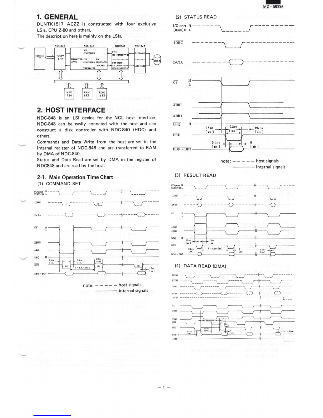
1.
GENERAL
DUNTK
1517
ACZZ
is
constructed
with
four
exclusive
LSis,
CPU
Z-80
and
others.
The description here
is
mainly
on
the LSis.
2.
HOST
INTERFACE
NDC-848
is
an
LSI
device
for
the
NCL
host interface.
NDC-848
can
be
easily conncted
with
the host
and
can
construct a disk
controller
with
NDC-840 (HOC)
and
others.
Commands
and
Data Write from the host
are
set in the
internal register
of N DC
-848
and
are
transferred
to
RAM
by
DMA
of
NDC-840.
Status
and
Data
Read
are
set
by
DMA
in the register
of
N DC848
and
are
read
by the host.
2-1. Main Operation Time Chart
(1)
COMMAND
SET
1/
0pon 11---
-,
,------
\
,------)}--
-"", ,
r-
---
(0383JH I.
\...
___
_J
~----'
~-----
IOWC
DATA
CS
ADI\0
ADRI
DRQ
H
IJoVR
UOO-UU7
---
--\
....
'.:'
.....~,------
-,\...
'~
.J~------n
-----\~
~
.Jr-
---
--
----
--c~------
--c=)------1)------c=
..
J---
----
note:
-----
host signals
-----internal
signals
- 1 -
-
MZ-5600A
(2) STATUS
READ
1/0
port
H-
----
-,
I----
---
-
--
[0380)
HL
\......
_____
...J
DATA
H
L
H
DDO~
DD7
-------,
,-------------
\_
__
_)
------
--z.-J-----
--------
25 ns
-I-~
0.31/J-:-
-1--
25 ns
[ oin ) [
1
"
[ o
in
)
0.
111
5 .... -
0
[ o
in)
[ o
in
)
r
note:
---
--
host signals
-----
internal signals
(3) RESULT READ
110
pon
ll
- - - - - - - - - -
~,
,,...
- - - -
-1~
- - -
-.
,
[0382
] H L
\.
............ /
\....
............
J
'-
.......
... J
\
...
Jr
............ - - -
....
""'\
....
...J,,...
- - - - -
-{J-
- -
.........
,L
.J,- - - - -
DATA
-----()----
-----{)--
- - - -
-H----
-{}-
-
----
(4)
DATA
READ
(DMA)
~
....
....
,\....
___
,.~
---
---""'
............
...J • .--
...........
-
--,'---
..J
r-
-----t--
"' . .._
___
F--
.............
----
'uc
Jto
......................... \ _____
/,_.
........ ---·\
...............
_, • .------,\... .............
_,
r--
Jt-
--
-------.~---
_, . .--
............
....
rnl'i:.'
------
--.\..._
..Jr------
--,'-- J
,,..------
---\
......
Jr-
-
-~-
-
-----.\...
...
J
',.....
... -----
•AT•
----
---
-c
:::>-----
-----c:::>------
----c:::>---+-------c)------
nnl
-----
------
----
-------
---------------n--
-------
-"'....
___
_
Page 3
-
MZ-5600A
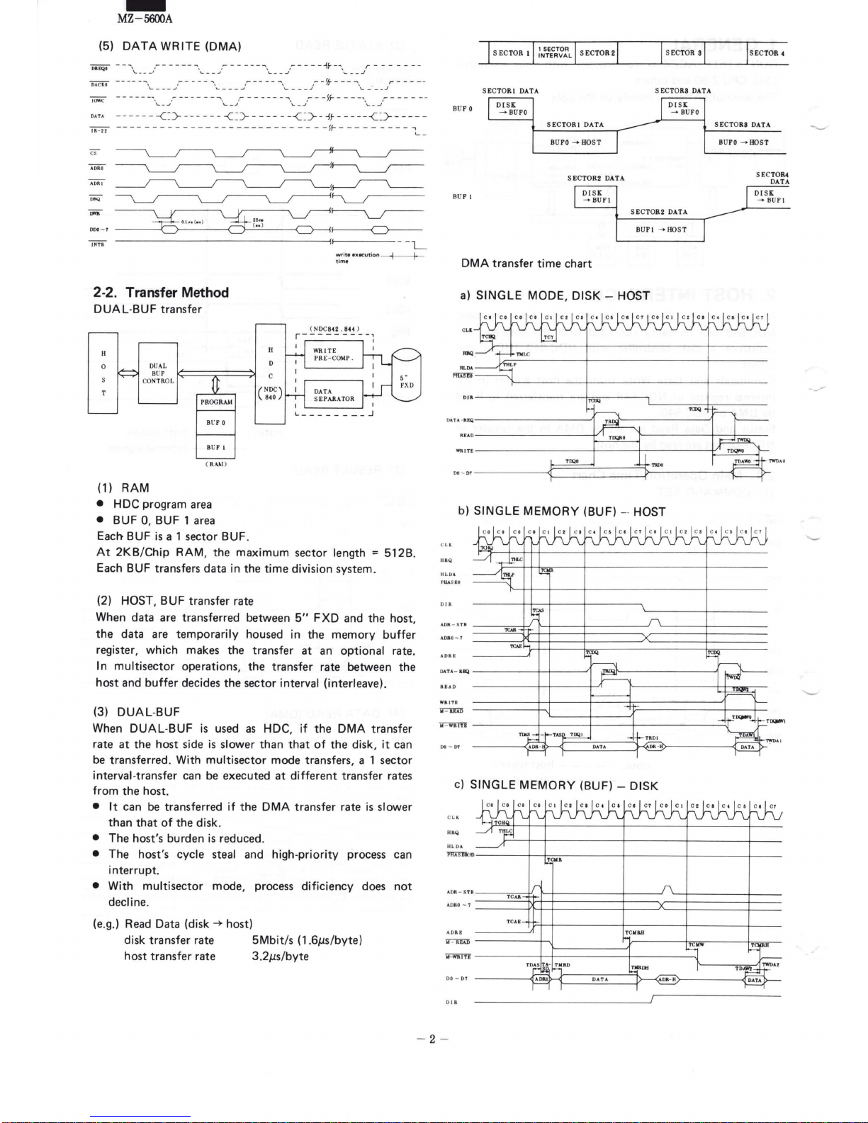
(5) DATA WRITE (DMA)
OI
UlQO --...
\ ........
_,'
..... -----...,
,....
- - -
.... --.\
__
...
_/,..
- - - -1f- --.,'-
...
...
Jr
- - - - - ......
"'i5ACi"a ----
...
...,\_---
. ./,...-
...... -'"'',
....
- - - J:
---
--
~
\
... ---
j
.....
-
~f-
-
--
'"""
·~
-·-
...
Jr -... ---
"--
....1
.....
----
- - ....... \.... .... J
......
- -
---
- .... \
...
-
J,
....
-
-jf--
- -
-
~
..........
_/.----
- -
...
DATA
-------CJ--------CJ----
-
---c:J---jf-------c:)------
~
----
---
- - -
---
--------
------ - !r---
- - -
---
;_ -
~
~
~~
~-
--.
~
~
~~--~
}~~
2-2. Transfer Method
DUAL-BUF
transfer
B
liF
I
( R All)
(1) RAM
• HDC
program
area
• BUF 0, BUF 1 area
Eac~
BUF
is
a 1
sector
BUF.
--L
wr
ite execution
-!--J.
-
ti
me
At
2KB/Chip
RAM,
the
maximum
sector
length =
5128
.
Each BUF
transfers
data
in
the
time
division
system.
(2) HOST, BUF
transfer
rate
When
data
are
transferred
between
5"
F XD
and
the
host
,
the
data
are
temporarily
housed
in
the
memory
buffer
register,
which
makes
the
transfer
at
an
optional
rate.
In
multisector
operations,
the
transfer
rate
between
the
host
and
buffer
decides
the
sector
interval (interleave).
(3) DUAL-BUF
When
DUAL
-BUF
is
used
as
HDC, if
the
DMA
transfer
rate
at
the
host
side
is
slower
than
that
of
the
disk,
it
can
be
transferred.
With
multisector
mode
transfers,
a 1
sector
interval -
transfer
can
be
executed
at
different
transfer
rates
from
the
host.
•
lt
can
be
transferred
if
the
DMA
transfer
rate
is
slower
than
that
of
the
disk .
•
The
host's
burden
is
reduced.
•
The
host's
cycle
steal
and
high-priority process
can
interrupt.
• With
multisector
mode,
process dificiency does
not
decline.
(e
.g.) Read Data
(disk~
host)
disk
transfer
rate
5Mbit/s
(1.6Ms/byte)
host
transfer
rate
3.2Ms/byte
SECTOR!
DATA
BUF 0
I
DI
SK
- au
ro
BUF I
S ECTO
R!
DATA
BUFO
~HOS
T
J
S ECTOR2 DATA
DISK
_,. BUrt
DMA
transfer
time
chart
SECTORS
DATA
I D I S K
~
BUFO
S ECTOR2
DATA
BUF I - HOS T
a)
SINGLE
MODE, DISK -
HOST
b)
SINGLE
MEMORY (BUF) -· HOST
C
L<
H
RQ
HLDA
P
W..
S£0
SEC
TOR 4
S ECTO
RB
OAT A
BUFO
-~>HOS
T
S ECTO
R4
D
ATA
DI
SK
- BUFI
ADR
-
STI=~~~~
ADI\0-1
ADA£
IlEA()
WR
ITE
ii="ifilj
c)
SINGLE
MEMORY
(BUF)-
DISK
C
LK
HRQ
HLOA
~m'-------~-+~~--------+---------~--------~
-----
Al>ft-S
TB=====~st======t=
==>
~~~====
t===
TCAR
ADRO
-1
- 2 -
Page 4
·-
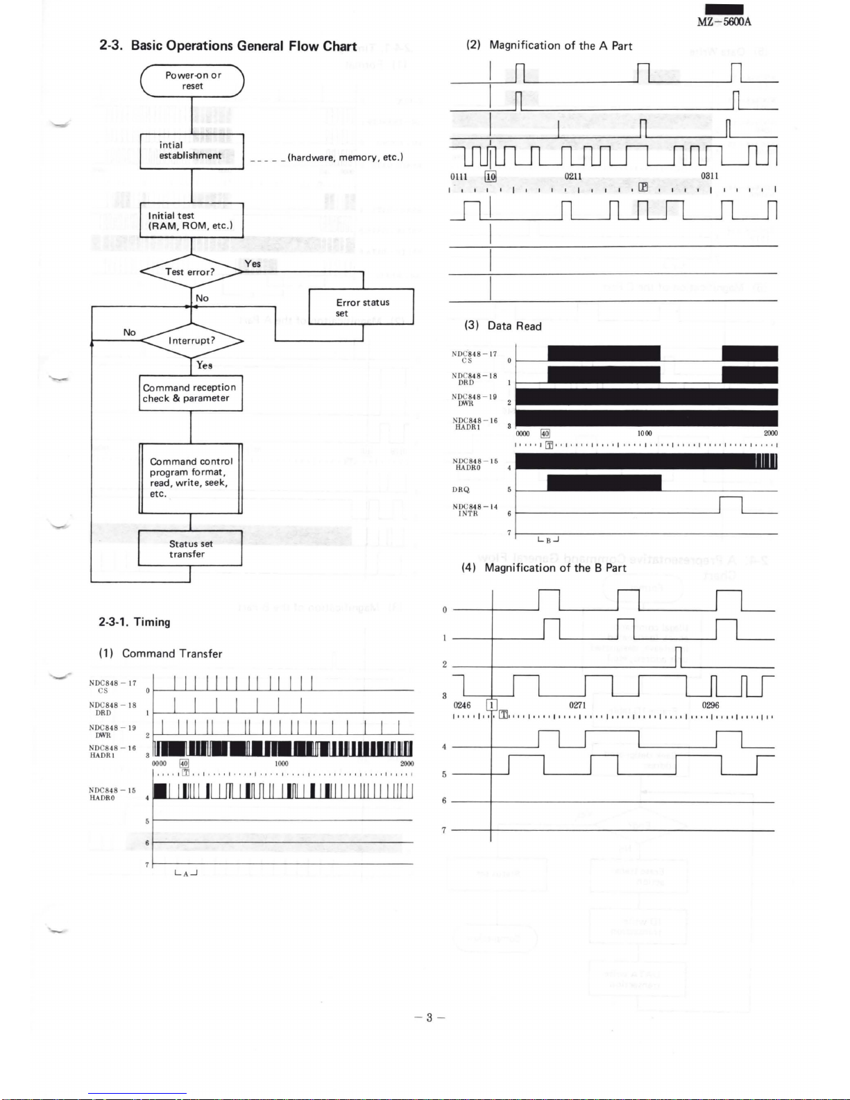
2-3. Basic Operations General Flow Chart
No
Power~n
or
reset
Command
control
program
format
,
read, write, seek,
etc
.
2-3-1.
Timing
(1) Command Transfer
NDC848-
17
CS
NDC848 - 18
DRD
NDC848 -
19
JJWR
NDC
848-
16
HADR1
NDC84
8-
15
HADRO
___
__
(hardware,
memory,
etc.}
2000
(2)
Magnification
of
the
A Part
-
MZ-5600A
.____
_
______.nL...__
_ ___,/L_
I I I I I I I I I
(3) Data
Read
NDC848 -
17
CS
NDC
848-
18
DRD
NDC848 - 19
DWI\
NDC848- 16
HADR1
I I I I
I I I I
1000
2000
I•
'''I
rl:l·· , ,
,,I,,
I'
•I
,,
''I'
I
''
I •
I'
I I I I ••
••••
'
I'
••
' I
NDC848 - 15
HADRO
DRQ
NDC848 - 14
INTR
(4)
Magnification
of
the B Part
0
--
-+--____J
3
0246
I 0271
0296
I•
I I I
,,
I I
[TI,
I I I I ' I I I I I I
••
I I I I I I I I I I I I I I I I I I I I I I I ' I I I I I I I I I I I I I I
5
6
------+-----------------------
----------------------
7
__
_,
____________
_______
___
- 3 -
Page 5
-
MZ-5600A
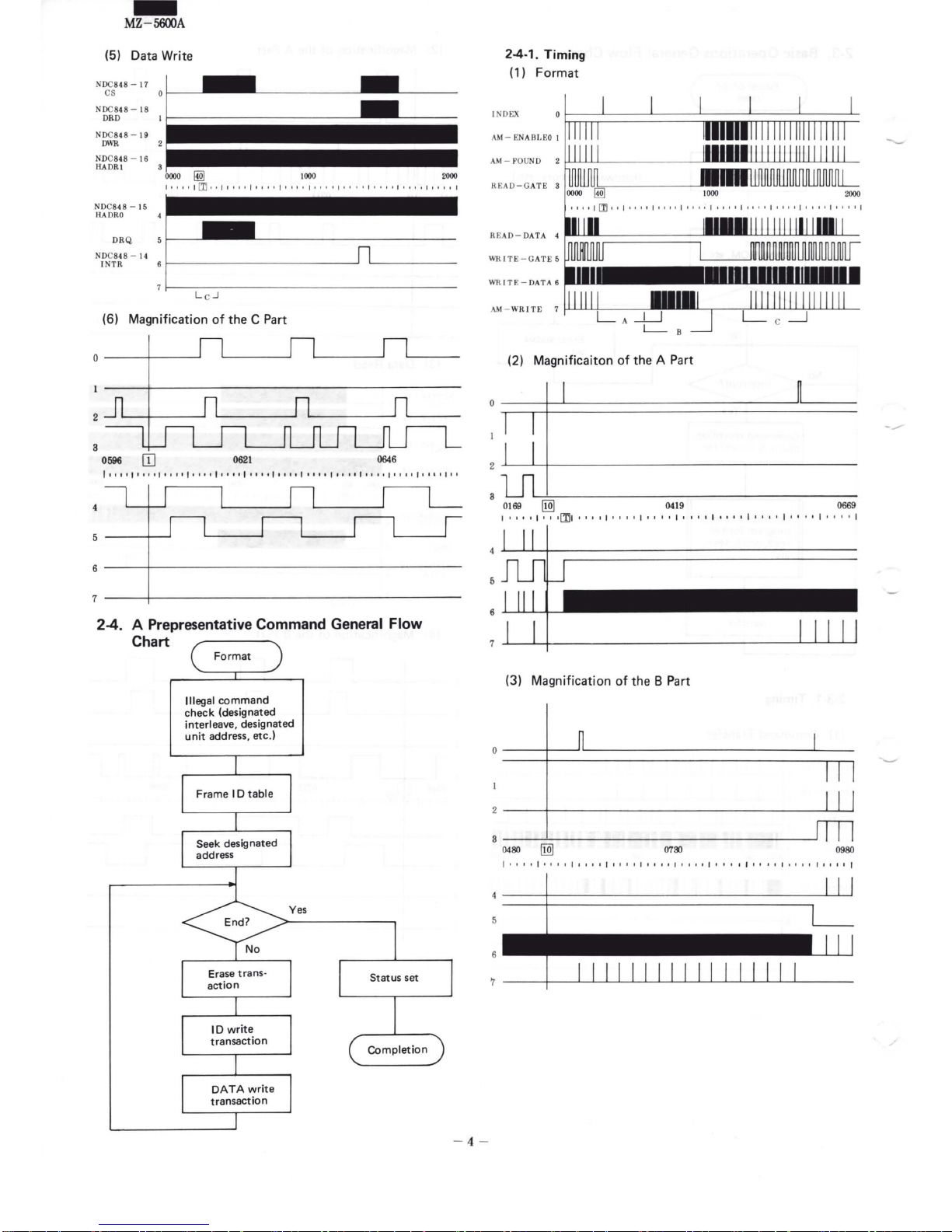
(5) Data Write
NDC848-17
CS
NDC848-18
DRD
NDC848 -
19
OWR
NDC848 -
16
HADRI
NDC848 -
15
HADRO
DRQ
NDC848 -
14
INTR
(6) Magnification
of
the C Part
2-4. A Prepresentative Command General Flow
Chart
Illegal
command
check
(desi
gnated
interleave, designated
unit address,
etc
.)
- 4 -
2-4-1. Timing
(1) Format
INDEX
AM-
ENABLEO I
AM
- FOUND
READ-G
ATE
3
READ-
DATA
4
WRITE-G
ATES
WRITE-D
ATA
6
(2) Magnificaiton
of
the A Part
2
a
0169
[!Q]
04
19 0669
I I I I I I I I
•[T}
I I I I I I I I I I I I I I I I I I I I I I I I I I I I I I I I I I I I I I I I I
5
6
7
(3) Magnification
of
the 8 Part
o---+~nL_
__
__________
____
,L_
_
Ill
2
--+-
--------------~
"
~
3--
~--------
----
----------nll
0480
[!Q]
0700
0980
I'
I I I I ' I I I I I I I I
I•
I I I I I I I I I I I I I I I I I I J I I I I
I'
I'
I I I I
11
I
Page 6
(4) Magnification
of
the
C Part
1
157
!.@]
1407
1
657
3.
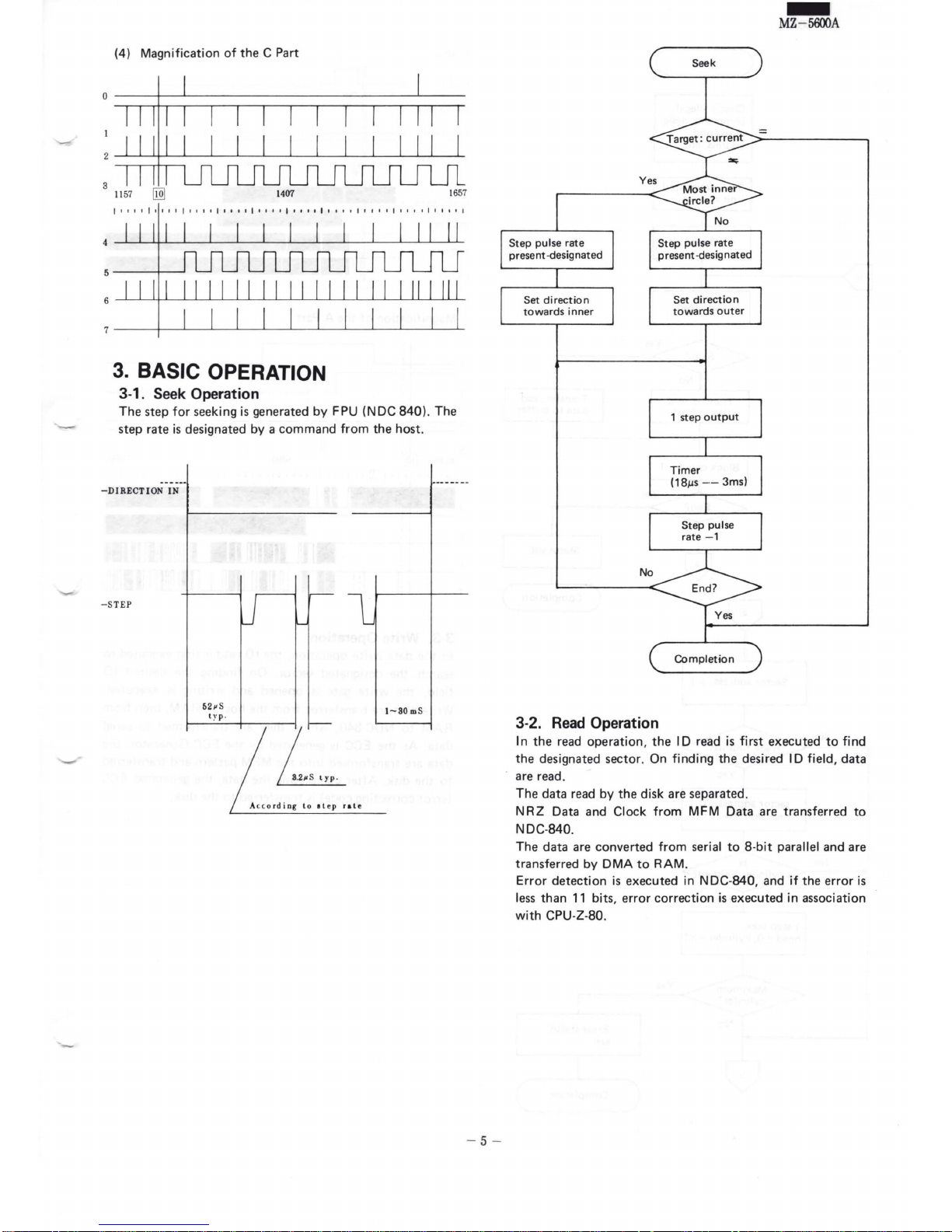
BASIC OPERATION
3-1.
Seek
Operation
The
step
for
seeking
is
generated by FPU (NDC
840).
The
step
rate is designated by a
command
from
the
host.
- DIRECTION I N
-STEP
1-80
mS
L
A
ccordi ng l o llep
rat
e
- 5 -
Seek
1
step
output
3-2.
Read
Operation
-
MZ-5600A
In
the
read
operation, the
ID read
is
first
executed
to
find
the
designated
sector
. On finding
the
desired
ID
field,
data
are read.
The
data
read by
the
disk are
separated.
NRZ
Data
and
Clock
from
MFM Data
are
transferred
to
NDC-840.
The
data
are
converted
from serial
to 8-bit
parallel
and
are
transferred
by DMA
to
RAM.
Error
detection
is
executed
in NDC-
840
, and if
the
error
is
less
than
11
bits,
error
correction
is
executed
in association
with
CPU-Z-80.
Page 7
b
-
MZ-5600A
Check
: illegal
command
, desig-
nated
unit
address, etc.
Sector
address + 1
No
No
1
step
seek
head =
0,
cylinder =
+1
Yes
- 6 -
READ
INDEX
AM-
ENABLEO I
AM-
FOlJND
READ-GA
TE 3
~
I
~
~
0000
:
rn
.. I··,. , .... , ... ,,
,,,,,,,
,,,,,,.,
..
,.,,,,,,
D
ATAO
DATA
l
L__A
___j
3
Magnification
of
the
A Part
I
I
I I
0
140
[Q]
'
0390
0640
, , . , . , ... , , m , , , , . , , , , , , , , , , , . , , , , , ,
..
, , , , , .. , , , ,
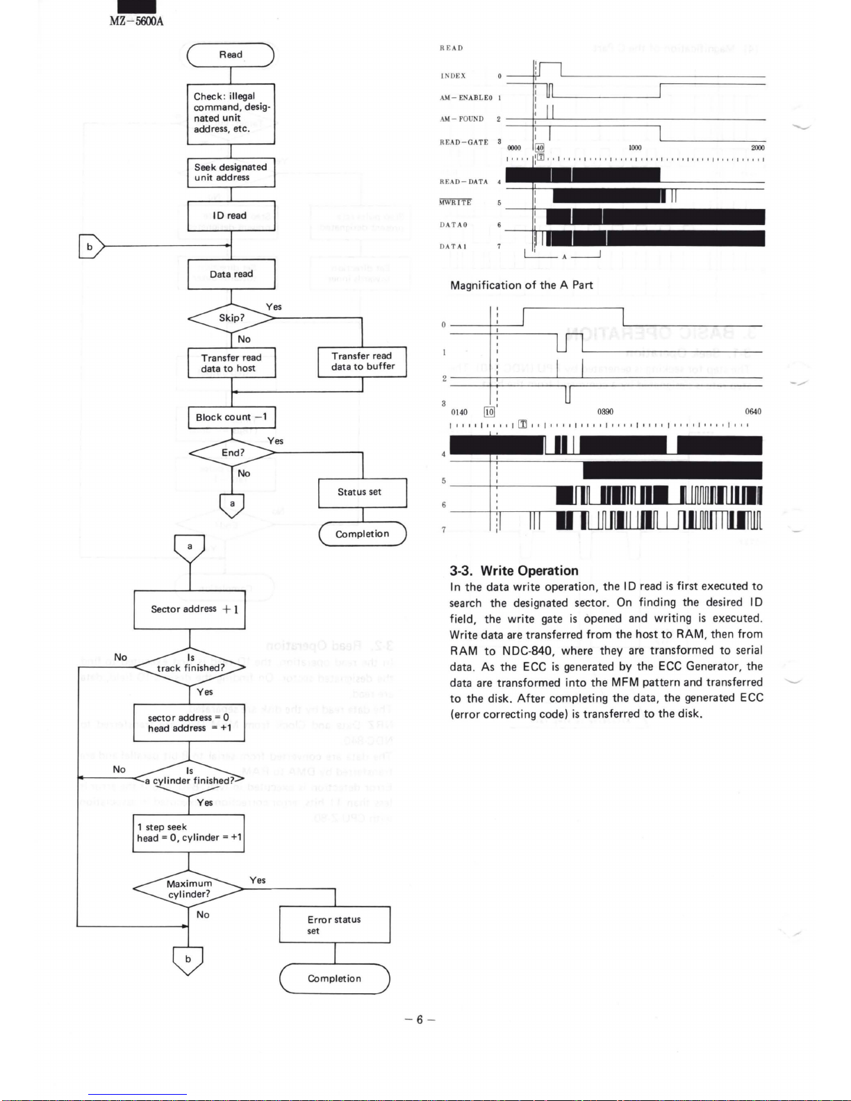
3-3. Write Operation
In
the
data
write
operation,
the
ID
read
is
first
executed
to
search
the
designated
sector
. On finding
the
desired
ID
field,
the
write
gate is
opened
and
writing
is
executed
.
Write
data
are
transferred
from
the
host
to
RAM,
then
from
RAM
to
NDC-840,
where
they
are
transformed
to
serial
data
. As
the
ECC
is
generated
by
the
ECC
Generator,
the
data
are
transformed
into
the
MFM
pattern
and
transferred
.._.,
to
the
disk.
After
completing
the
data, the
generated
ECC
(error
correcting
code)
is
transferred
to
the
disk.
Page 8
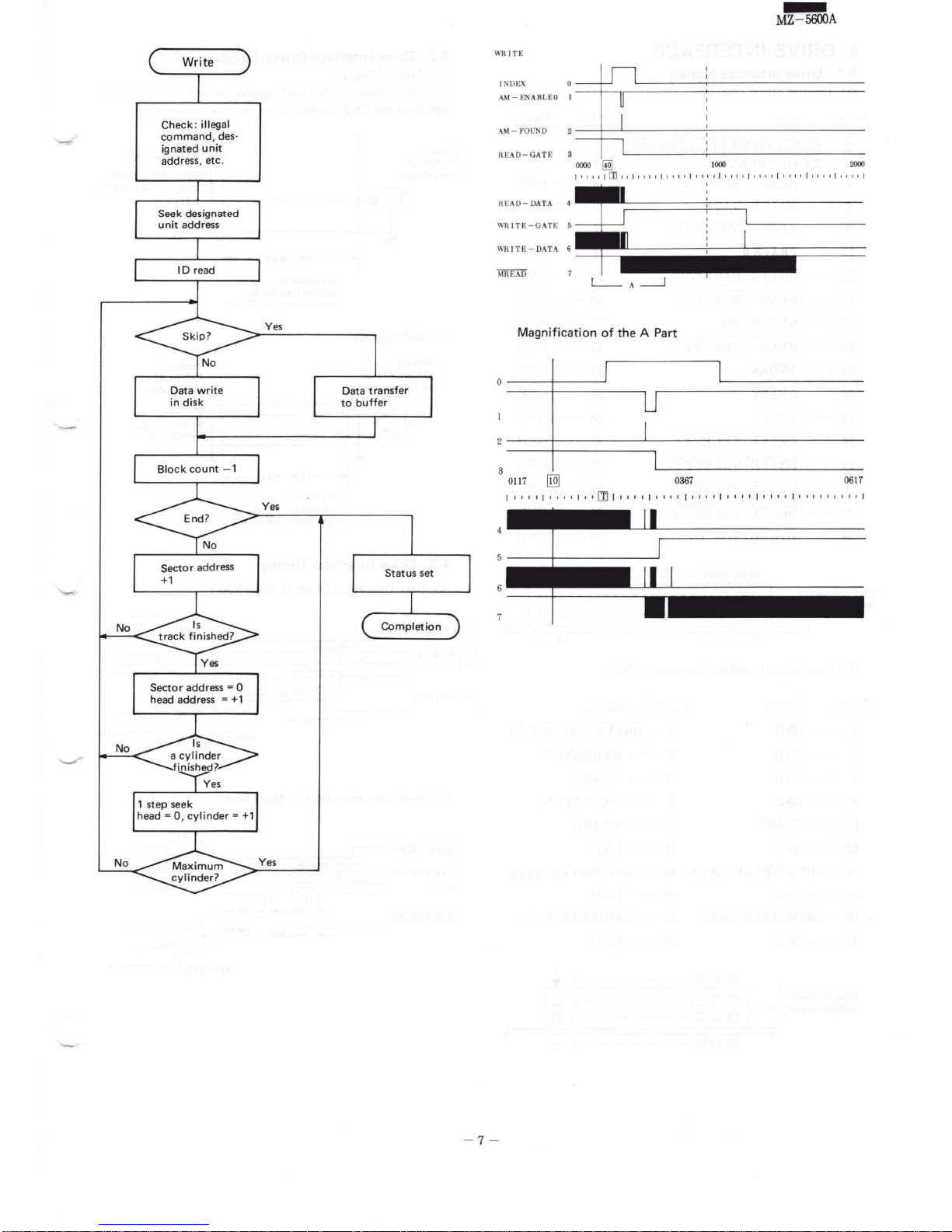
No
No
No
-
Check : illegal
command,
designated unit
address, etc.
WR
IT E
I N
DEX
AM
- ENABLEO
AM
- FOUND
RE
AD-GATE
RE
AD-
DATA
WRITE-DATA
6
-
MZ-5600A
0000
~
I
000
2000
,,,
, , r
LrJ
,,,,,,,
r,, ,,,,,,,,,
' '
,,,,,,,,
'''
I•
•' ,,,, ,,,
'
l__
A
__j
Magnification
of
the A Part
0
--t----''
I
2
--~---~'----------
3
I
0117
0367
0617
, . , .. , , , , , , . , m, , . , , , .... , . , , . ,
..
, , , . ,
..
, .. , . , ,
..
, ,
- 7 -
Page 9
-
MZ-5600A
4.
DRIVE INTERFACE
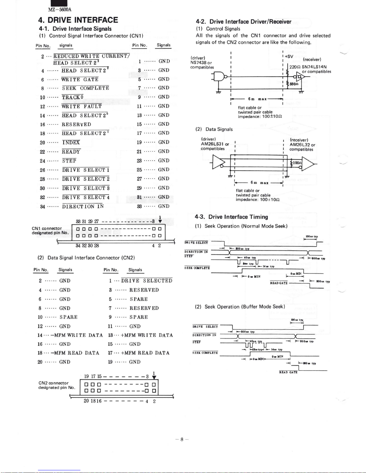
4-1. Drive Interface Signals
(1) Control Signal Interface Connector (CN1)
Pin
No.
signals Pin
No.
Signals
2 · · ·
REDUCED
WRITE
CURRENT
I
HEAD
SELECT
2
3
1
GND
GND
GND
GND
4
HEAD
SELECT2
2
3
6
8
10 ....
..
12 ...
.. .
14 .
.....
16 ......
18 ....
. .
20 ....
. .
22
....
..
24 ..... .
26
····
··
28
... ...
30 . . .
...
32 . .....
84
...
...
WRITE
GATE
SEEK
COMPLETE
TRACKO
WRITE
FAULT
HEAD
SELECT
2°
RESERVED
HEAD
SELECT
2
1
INDEX
READY
STEP
DRIVE
SELECT
1
DRIVE
SELECT
2
DRIVE
SELECT
3
DRIVE
SELECT
4
DIRECT
ION
IN
5
7
9 GND
11 ···
···
GND
13 ······ GND
15
·····
· GND
17 ·····
· GND
19
·····
· GND
21 ····· · GND
23 ·····
· GND
25
··
·· ··
GND
?:l ···
···
GND
29
···
···
GND
81 ······ GND
33
····· · GND
1
33
31
2}
'Zl
- - - - - - - • - - - - - -8
~
CN1
connector
designated
pin
No.
o o o o
--------------0
o I
0 0 0
0--------------0
0.
84
32
30
28
4 2
(2) Data Signal Interface Connector (CN2)
Pin No.
Signals
Pin No .
Signals
2 GND
1 .
..
DRIVE
SELECTED
4
GND 3
RESERVED
6 GND
5
SPARE
8 GND 7
RESERVED
10
......
SPARE
9
SPARE
12 ......
GND
11
......
GND
14
...
-MFM
WRITE
DATA
13 ... +MFM
WRITE
DATA
16
..
..
..
GND
15
.. · ..
· GND
18 ...
-MFM
READ DATA
17 ...
+MFM
READ
DATA
20 ....
..
GND
CN2 connector
designated
pin
No .
t
19
......
GND
19
17
15
- - - - - - - 3
ODD
--------o
ODD
--------0
20 1816 - - - - - - - 4 2
4-2. Drive Interface Driver/Receiver
( 1) Control Signals
All
the signals
of
the
CN1
connector and drive selected
signals
of
the CN2 connector
are
like the
following
.
I
(driver)
NS7438
or
compatibles
I +SV
I
(receiver)
I
t---
6m
max--,
I I
(2) Data Signals
(driver)
AM26LS31
or
:
compatibles
I
flat
cable
or
twisted pair cable
impedance:
100±10.n
-
I
6m
max---'
I
flat
cable
or
twisted pair cable
impedance: 100±10.n
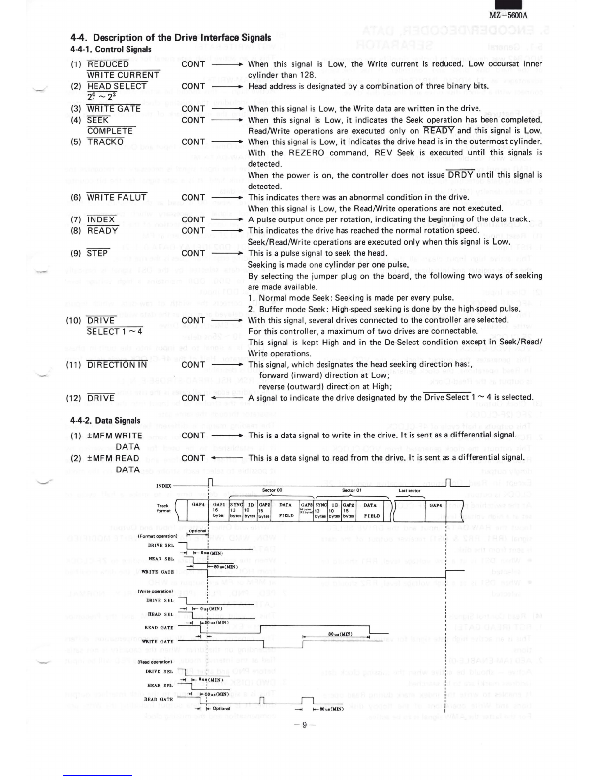
4-3. Drive Interface Timing
(1) Seek Operation (Normal Mode Seek)
(receiver)
AM26L32
or
compatibles
DRIVE
SELECT
DIRE
CTION IN
S'fEP
~
I--
IOOu trp
--~X
~
--1
-
eo
..
'"
--1
1-aoo.
,,
~----~
:-;S E""
EJ[
;;;-
OCAI=P=-:L-=:ET=E
~
IC,. 1n>
--i
-O•JoiiN
--:REA_D_G-AT-E
~In>
(2)
Seek
Operation
(Buffer
Mode Seek)
DRIVE SELECT
--l
1--IOOu
trp
DIRECTION IN
=:J~;----------,-'X'----
_
--~;.;__
......
Ouo
!n.
-l
~
lOO•
In>
UlJ-
~
.....,
~--ta-t,.poo~
t--
14u.
'"
S
EU
C<»>PLETE
____
....J
-~·~·~Joi~IN~~L------
-l
t-O•MINI--
-1
l-IDO•
In>
I
READ
GATE.__
___
_
- 8 -
-
----
Page 10
-
MZ-5600A
4-4. Description
of
the Drive Interface
Signals
4-4-1. Control Signals
( 1)
REDUCED
WRITE
CURRENT
(2)
HEAD
SELECT
2?-
2
2
(3)
WRITE GATE
(4)
SEEK
COMPLETE
(5)
TRACKO
(6)
WRITE
FALUT
(7)
INDEX
(8)
READY
(9)
STEP
(10) DRIVE
SELECT1
- 4
(11)
DIRECTIONIN
(12) DRIVE
4-4-2. Data Signals
(1)
±MFMWRITE
DATA
(2)
±MFM
READ
DATA
CONT
CONT
CONT
CONT
CONT
CONT
CONT
CONT
CONT
CONT
CONT
CONT
CONT
CONT
When
this
signal is Low,
the
Write
current
is
reduced.
Low
occursat
inner
cylinder
than 128
.
Head address
is
designated
by a combination
of
three
binary
bits.
When
this
signal
is
Low,
the
Write
data
are
written
in
the
drive.
When
this sign
al
is Low ,
it
indicates
the
Seek
operation
has
been
completed
.
Read/Write
ope
rati
ons
are
executed
only
on
READY
and
this signal
is
Low.
When this sign
al
is
Low, it indicates
the
drive head
is
in
the
outermost
cylinder.
With
the
REZERO
command, REV
Seek
is
executed
until
this
signals
is
detected
.
When
the
power is on,
the
controller
does
not
issue
DRDY
until
this
signal
is
detected.
This
indicate
s there was an
abnormal
condition
in
the
drive.
When
this
signal
is
Low,
the
Read/Write
operations
are
not
executed.
A pulse
output once
per
rotation,
indicating
the
beginning
of
the
data
track.
This
indicates the
drive has reached
the
normal
rotation
speed.
Seek/Read/Write
operations
are
executed
only
when
this
signal
is
Low.
This
is
a pulse signal
to
seek
the
head.
Seeking
is
made
one
cylinder
per
one
pulse.
By
selecting the j
umper
plug on
the
board, the
following
two
ways
of
seeking
are
made
available .
1. Normal
mode
Seek
: Seeking
is
made
per
every pulse.
2. Buffer
mode
Seek: High -
speed
seeking
is
done
by
the
high-speed pulse.
With
this
signa
l,
several drives
connected
to
the
controller
are
selected
.
For
this
controller, a
maximum
of
two
drives are
connectable
.
This signal
is kep
t High
and
in
the De-
Select
condition
except
in
Seek/Read/
Write
operat
ions.
---
This signal, which designates
the
head seeking
direction
has:,
forward
(inward)
direction
at
Low;
reverse
(outward)
direction
at
High;
A signal
to
indicat e
the
drive
designated
by
the
Drive
Select
1 - 4
is
selected
.
This
is a data
signal
to
write
in
the
drive.
lt
is
sent
as a differential signal.
This
is a data
signal
to
read
from
the
drive.
lt
is
sent
as a differential
signal.
IN
DEX
----!
'-------....,.,...-
---
----,----------.1
Sector
00
Sector
01
l
•t
aector
,-,-~--~=;~==~==~~~~~;===~~----'~~~
~~
___l____..l._~
__L____._l__l(
I Gm I (
Track
format
{Fo
i1'N
t operet ion)
1
0ptione
l~
:
DR
IT E S E L
HEAD
SEL
WR
ITE OA
TE
{W
rite
o~tion
)
DRIVE
SEL
BEAD
SEL
'
'
'
--f
.._O
.. (lUN
)
!i
--t
1-&0u•(lO
N)
--t
t-50u•OHN)
READ GA
TE
~~+
:
____
__J
WRITE OATE
__
-4-'--Tt---
----,
I
Reed
operation)
DRIVE S
EL
---,
:
-t
t-
Oua,(MJN)
IIEADSEL
~
-+1
,._50u•(W:IN
)
8
0-..
(MIN)
READ GATE
~
L..;..:
____
__.JnL. ___
..JnL
_ _ _
-t
;..._
Optional
---t
1-
80
Ul
(
)f]N
)
- 9 -
Page 11
-
MZ-5600A
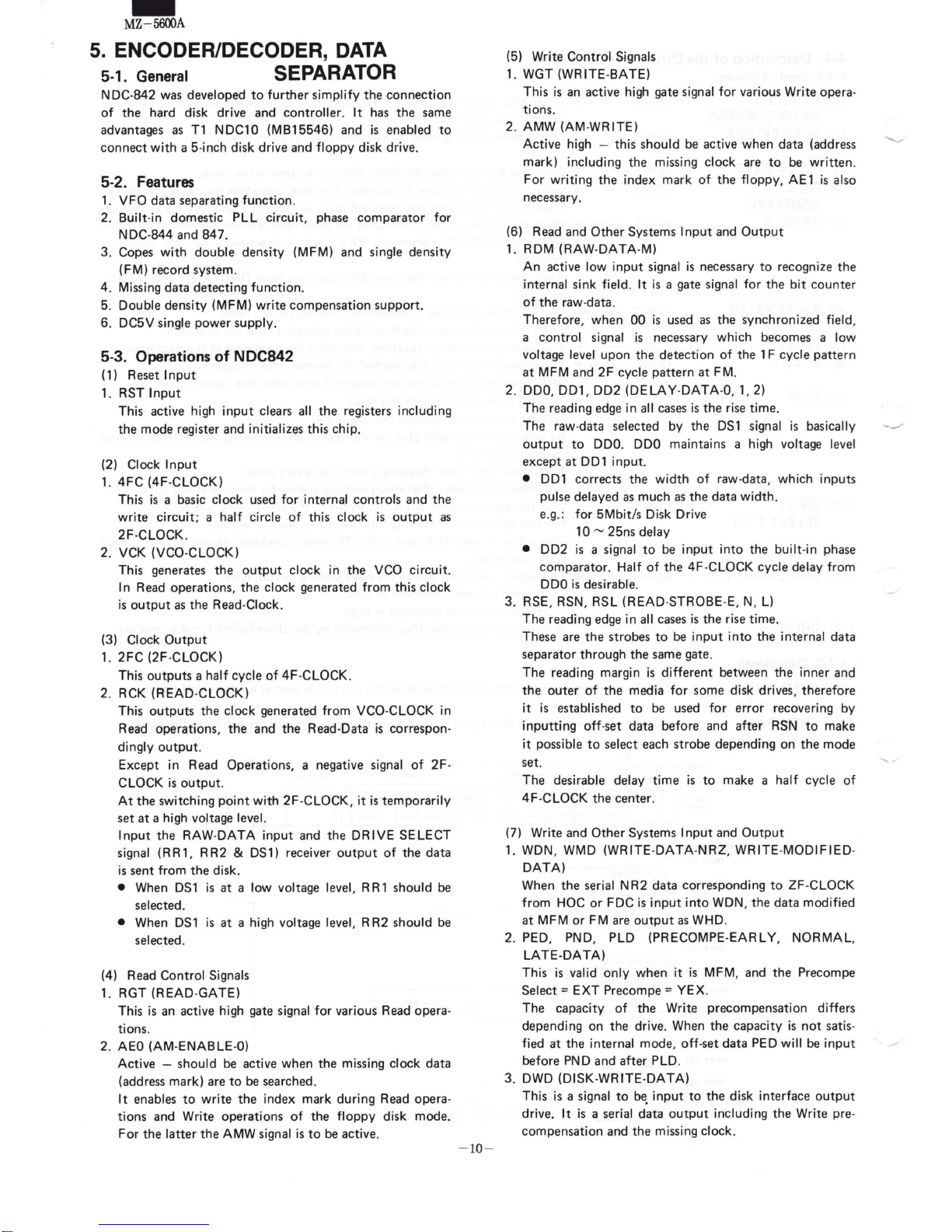
5. ENCODER/DECODER,
DATA
5-1.
General
SEPARATOR
NDC-842 was
developed
to
further
simplify
the
connection
of
the
hard
disk drive
and
controller. it
has
the
same
advantages as
T1
NDC10
(MB15546)
and
is
enabled
to
connect
with
a 5 -inch disk drive
and
floppy
disk drive.
5-2.
Features
1.
VFO
data
separating
function.
2. Built-in
domestic
PLL
circuit,
phase
comparator
for
N DC-844
and
84
7.
3.
Copes wi
th
double
density
(MFM)
and
single
density
(FM)
record
system.
4. Missing
data
detecting
function
.
5.
Double
density
(MFM)
write
compensation
support
.
6.
DC5V single
power
supply.
5-3. Operations
of
NDC842
(1) Reset
Input
1.
RST
Input
This active high
input
clears
all
the
registers including
the
mode
register and initializes
this
chip.
(2)
Clock
Input
1.
4FC
(4F-CLOCK)
This
is
a basic
clock
used
for
internal
controls
and
the
write
circuit; a half
circle
of
this
clock
is
output
as
2F-CLOCK .
2. VCK (VCO-CLOCK)
This
generates
the
output
clock
in
the
VCO
circuit
.
In Read
operations,
the
clock
generated
from
this
clock
is
output
as
the
Read-Clock.
(3) Clock
Output
1.
2FC
(2F-CLOCK)
This
outputs
a half
cycle
of
4F-CLOCK.
2. RCK (READ-CLOCK)
This
outputs
the
clock
generated
from
VCO-CLOCK in
Read
operations,
the
and
the
Read-Data
is
correspon
-
dingly
output
.
Except
in Read
Operations,
a negative signal
of
2F-
CLOCK
is
output.
At
the
switching
point
with 2F-CLOCK, it
is
temporarily
set
at
a high voltage level.
Input
the
RAW-DATA
input
and
the
DRIVE
SELECT
signal
(RR1,
RR2
& DS1) receiver
output
of
the
data
is
sent
from
the
disk.
• When
DS1
is
at
a low voltage level , R R 1
should
be
selected.
•
When
DS 1 is
at
a high voltage level, R R2
should
be
selected.
(4) Read
Control
Signals
1.
RGT
(READ-GATE)
This
is
an active high gate signal
for
various Read
opera-
tions
.
2. AEO (AM-ENABLE-D)
Active -
should
be active
when
the
missing
clock
data
(address
mark)
are
to
be
searched
.
it
enables
to
write
the
index
mark
during
Read
opera
-
tions
and
Write
operations
of
the
floppy
disk
mode.
For
the
latter
the
AMW signal
is
to
be active.
-10-
(5) Write
Control
Signals
1. WGT (WRITE -BATE)
This
is
an active high gate signal
for
various Write opera-
tions
.
2. AMW
(AM-WRITE)
Active high - this
should
be active
when
data
(address
mark)
including
the
missing
clock
are
to
be
written
.
For
writing
the
index
mark
of
the
floppy,
AE1
is
also
necessary.
(6) Read
and
Other
Systems
Input
and
Output
1. RDM (RAW-DATA-M)
An
active low
input
signal
is
necessary
to
recognize
the
internal sink field.
it
is
a gate signal
for
the
bit
counter
of
the
raw-
data
.
Therefore,
when
00
is
used
as
the
synchronized
field,
a
control
signal
is
necessary
which
becomes
a low
voltage level
upon
the
detection
of
the
1 F
cycle
pattern
at M FM
and
2 F cycle
pattern
at
FM.
2. DDO, DD1,
DD2
(DELAY-DATA-0, 1, 2)
The
reading edge in all cases
is
the
rise
time.
The
raw-data
selected
by
the
DS1
signal
is
basically
output
to
DDO. DDO
maintains
a high voltage level
except
at
DD1
input
.
• DD1
corrects
the
width
of
raw-data,
which
inputs
pulse
delayed
as
much
as
the
data width.
e.g.:
for
5Mbit/s
Disk Drive
10-
25ns
delay
•
DD2
is
a signal
to
be
input
into
the
built
-in phase
comparator.
Half
of
the 4F-CLOCK
cycle
delay
from
DDO
is
desirable.
3.
RSE, RSN , RSL (READ-STROBE-E,
N,
L)
The
reading edge in all cases
is
the
rise
time
.
These
are
the
strobes
to
be
input
into
the
internal
data
separator
through
the
same
gate.
The
reading margin
is
different
between
the
inner
and
the
outer
of
the
media
for
some
disk drives,
therefore
it
is
established
to
be used
for
error
recovering
by
inputting
off-set
data
before
and
after
RSN
to
make
it possible
to
select
each
strobe
depending
on
the
mode
set.
The
desirable delay
time
is
to
make a half
cycle
of
4F-CLOCK
the
center.
(7) Write and
Other
Systems
Input
and
Output
1. WDN, WMD (WRITE-DATA-NRZ, WRITE-
MODIFIED
DATA)
When
the
serial N R2
data
corresponding
to
ZF-CLOCK
from
HOC
or
FDC
is
input
into
WDN ,
the
data
modified
at
MFM
or
FM are
output
as WHD.
2.
PED, PND, PLD
(PRECOMPE-EARLY
, NORMAL,
LATE-DATA)
This
is
valid
only
when
it
is
MFM,
and
the
Precompe
Select=
EXT
Precompe
= YEX.
The
capacity
of
the
Write
precompensation
differs
depending
on
the
drive. When
the
capacity
is
not
satis-
fied
at
the
internal
mode,
off-set
data
PED will be
input
before
PND
and
after
PLD .
3.
DWD (DISK-WRITE-DATA)
This
is
a signal
to
b~
input
to
the
disk
interface
output
drive.
it
is
a serial
data
output
including
the
Write
pre
compensation
and
the
missing
clock
.
Page 12
(8) Write Precompensation Detecting Pattern
The precompensation
bit
pattern
is
shown below.
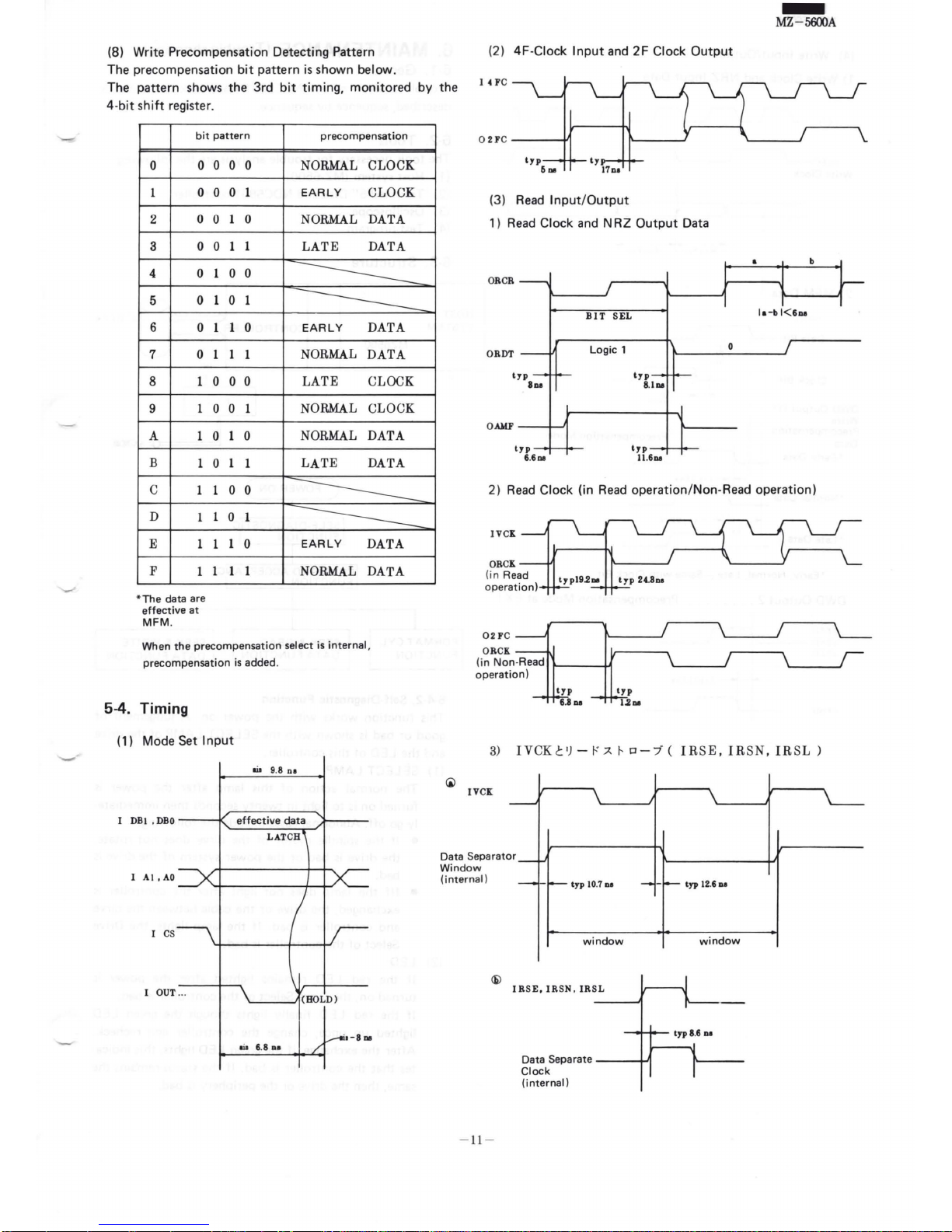
(2) 4F-Ciock
Input
and 2F Clock
Output
-
MZ-5600A
The pattern shows the 3rd
bit
timing,
monitored by the
4-
bit
shift
register.
bit
pattern
0 0
1
0
2
0
3
0
4 0
5
0
6
0
7
0
8
1
9
1
A
1
B
1
c 1
D
1
E 1
F
1
*Th
e data are
effective
at
MFM
.
0 0 0
0 0
1
0
1 0
0
1
1
1
0 0
1 0 1
1 1
0
1 1
1
0 0 0
0
0 1
0 1 0
0
1
1
1
0
0
1
0
1
1
1
0
1 1 1
precompensation
NORMAL
CLOCK
EARLY
CLOCK
NORMAL
DATA
LATE
DATA
-----
-------
EARLY
DATA
NORMAL
DATA
LATE
CLOCK
NORMAL
CLOCK
NORMAL
DATA
LATE
DATA
----
-----
EARLY
DATA
NORMAL
DATA
When
the
precompensation select is
internal,
precompensation
is
added.
5-4. Timing
(
1)
Mode Set
Input
oil 9.8
no
I
AI,
AO
I
CS
'----JI(HOLD)
·
·-8
Dl
oil 6.8
Dl
(3)
Read
Input/Output
1)
Read
Clock and N RZ
Output
Data
•
b
ORCR
~
I
v---
BIT
SEL
lo-b
I<&DO
logic
1
0
I
-
ORDT
yp-
~
lyp-
1--
8DO
8.101
OAMF
7P
lyp
&.&no
11.6no
2)
Read
Clock (in
Read
operation/Non-
Read
operation)
02
FC
~
~
r
\'----------.1/
~
ORCK
r---~
(in
Non
-Read
--+1
\.._
__
.-~/
\'----'
operation)
lyp
lyp
6.8
DO
1.2no
3)
I V
CK
c
')
-
f:
.7.
I-
o - 7 ( I R
SE
, I R S
N,
I R S L )
IVCK
--J
Data Separate
Window
(interna
l)
r_
\
lyp 10.7
Dl
window
I
RSE,
IRSN.
IRSL
--
- - lyp
12.6
DO
window
.I
\.
----if-+--
lyp 8.8 DO
-11-
Data Separate
---l..IJ
Clock
(internal)
\
I
Page 13
-
MZ-5600A
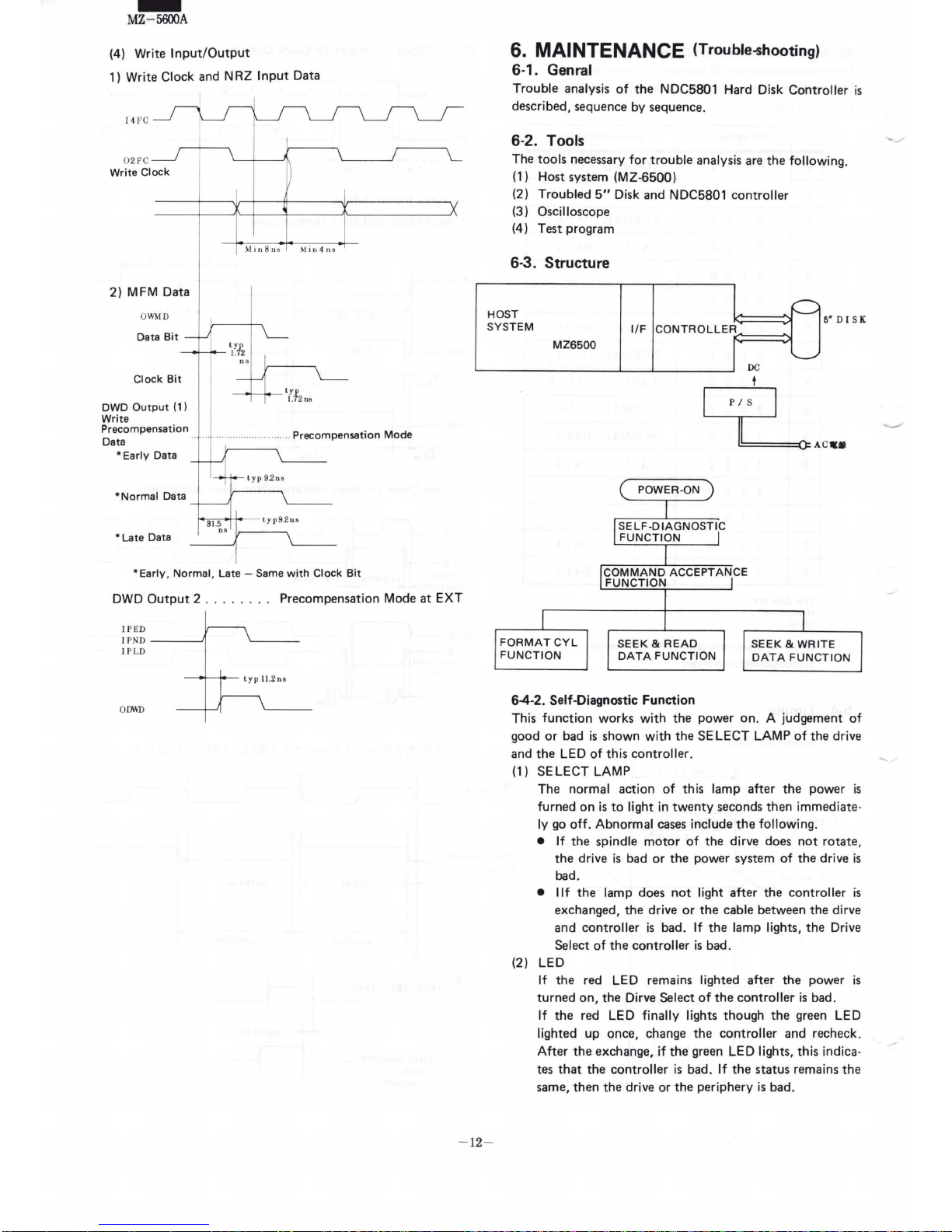
(4) Write
Input/Output
1)
Write Clock
and N RZ
Input
Data
14
FC
0
2F
C
Write Clock
2) MFM Data
OWMD
Data
Bit
Clock
Bit
DWD
Output
(1)
Write
M
in8n
::s
M
in
4 n s
Precompensation
Data
··
..................
........
..... Precompensation Mode
*Early
Data
*Normal
Data
*Late
Data
* Early,
Normal,
Late-
Same
with
Clock
Bit
DWD
Output
2 . . . . . . . . Precompensation Mode at
EXT
IPED
IPND
---..J
I
!PLO
ODWD
6.
MAINTENANCE (Trouble-ihooting)
6-1. Genral
Trouble analysis
of
the NDC5801 Hard Disk Controller
is
described, sequence by sequence.
6-2. Tools
The tools necessary
for
trouble analysis
are
the
following
.
(1) Host system (MZ-6500)
(2) Troubled
5"
Disk and NDC5801 controller
(3) Oscilloscope
(4) Test program
6-3. Structure
I
r---
HOST
r------
SYSTEM
1/F
CONTROLLER
6"
D l S K
MZ6500
I
DC
6-4-2. Self-Diagnostic Function
This
function
works
with
the power on. A judgement
of
good
or
bad
is
shown
with
the SELECT LAMP
of
the drive
and the LED
of
this controller.
(1) SELECT LAMP
The
normal action
of
this lamp after the power
is
turned on
is
to
light in
twenty
seconds
then immediate·
ly
go
off.
Abnormal
cases
include the following.
•
If
the spindle
motor
of
the dirve
does
not
rotate,
the drive
is
bad
or
the power system
of
the drive
is
bad.
•
llf
the lamp
does
not
light after the controller
is
exchanged, the drive
or
the cable between the dirve
and
controller
is
bad.
If
the lamp lights, the Drive
Select
of
the controller
is
bad.
(2) LED
If
the red LED remains lighted after the power
is
turned on, the Dirve Select
of
the controller
is
bad.
If
the red LED
finally
lights though the
green
LED
lighted up once, change the controller and recheck.
After
the exchange,
if
the
green
LED lights, this indica-
tes
that
the controller
is
bad.
If
the status remains the
same,
then the drive or the periphery
is
bad
.
-12-
Page 14

._
6-4-3.
Basic
Operations
of
the Controller
To check
if
the self-diagnosis
is
executing normally after
the
controller
is
turned on
or
reset:
( 1)
If
the red LED remains lighted after the power
is
on or
reset.
CD
Confirm
if
the MPU Z-80 39PIN
READ
signal
is
output
after
eset
.
(ID
MPU Z-80 39PIN
CLK
is
normal
or
2.5MHz.
• 26LS31 (5F)
is
bad.
• 74LS74 (5C)
is
bad
.
• NDC842 (7G)
is
bad
.
•
OSC
(6G)
is
bad. 10MHz
@
Is
the RESET signal at High?
•
TL7700
(&B) and the peripheral
circuit
are
bad
.
• RESET
from
the host and the
circuit
are
bad.
• NDC848
is
bad.
(2)
If
the red LED remains lighted after the
green
LED
lights
with
the power on
or
reset,
CD
Change
the controller and reconfirm.
•
If
the green LED lights after the change, this indicates
that
the controller
is
bad
.
•
If
the status remains the
same,
then the drive
or
the
periphery
is
bad.
6-4-4. Operation Check
with
the Self-Diagnostic Switch
(1)
Read
Test
•
RD
(SW3) switch
is
ON.
• ST (SW1)
switch
is
ON.
CD
If
the NG lamp doe
:;
not
light
unitl
15 minutes after the
switch
is
on,
•
lt
can
be
judged
that
the
Read
system
is
normal.
6-4-5. Impossibility
of
Command Acceptance
(1) Host Interface Circuits
RC
SET
Ill
.Aa
AJ
~~
'~
ts-'1!
I
;}.,
_s,lSIU_f
6\110-
~'!
11.
y
8
•
~
~J1
~
-
® The
NG
lamp lights:
-
MZ-5600A
a)
Confirm NDC847 (8G) Pin 2,
13-5V.
•
TL497
(88)
is
bad.
• Peripheral
circuit
of
TL497
is
bad.
b) Confirm NDC847 (8G) Pin
8t{).5V±2.0V
• NDC847
is
bad.
c) Confirm the REad data from the disk.
• NDC842 (7G)
is
bad.
• NDC840 (4E)
is
bad.
• NDC846 (4G)
is
bad.
•
74LS123(8H)isbad.
• 26LS32 (5E)
is
bad.
• N DC84 7 (8G)
is
bad.
d)
74LS123 (8H) Pin 12:
• Confirm Low level at 260ns+30ns.
(2) Write Test
•
RW
(SW4) switch
is
ON.
• ST (SW1)
switch
is
ON.
CD
If
the NG lamp
does
not
light
until
15 minutes after the
switch
is
on,
•
lt
can
be judged
that
both the
Read
and Write
sys-
tems
are
normal.
® The
NG
lamp lights:
a)
If
the
Read
system
is
normal,
it
can
be
judged
that
the Write system
is
abnormal.
•
NDC842 (7G)
is
bad.
• NDC840 (4E)
is
bad.
• NDC846 (4G)
is
bad.
• 74LS38 (6C)
is
bad.
• 26LS31 (5F)
is
bad.
~-
se
"''
~~
AI
Y~
wn·,
I I
~
•. , oft
w
;.~
,~~
~·
l.bo:"'
~
-:-::
~
~
lA
r11
11
VT:JJ
68
-
-
t;:JC.:rc
/1.6
AS
M
~
~
~
X1ll'Jr
~
~A
I
.1
,,_,
l:tSGf
r---
~
..,
I
...WXJIL,
·a·
7£1
18..r
CS
~
r
91.&
~rr=~
•
::zax:
~-:::
A y
F.f
~
~
I
::
~
9
..
~
All@
._.,
~
'-
.-d.K./
811
..
!If
tell!!ll
81
~
_l
~o
8
~
6A
=~
I·
/:<re~
~
817
5B
()RQ
lt
L1!l
11.1:1
INr.
88
lYNSe
~
CJ,llf.F
M
014
OIJ
()I;>
011
01.
fl
01
06
os
C><J
DJ
02
01
{)N
:m
·u
-m
A e
HD1
A'.:
:!
JA
'!:!:
~
HOJ
IPl
._HO;>
1\2
~
;;
-
~--~
c
.13
l:s'm
~Jt,
~
11
8
;;;
fll
8~
Al3
~
DtR
r:
ts;;;s
-13-
Page 15

-
MZ-5600A
(2) H t I terface LSis
os
n
r~
~5
~-
HOJ
Hr).;>
<D~
~
(~
llf]R
~
~~HA~}
(
DR.b
~
~R
...I,JD
~-
,.:K"_n
""""''""'
RMI
1~
j~.;>Kn•l
rxr
"I
r5re
r
~Ls
l
-a!:::
_8.
·~·
:RJ
[IC
~
~"-~
~
_,..,.,~<D®
..11.
NOC848
'~11
.naru
~
18
........
""A\
-
_(J;
'':!:.
?Nti~
:Bz1t>
.IJ.
31_
JJ
'•IOSII"fi'O
~
_LC
_15
NC
JtJ
NC
lM:
_/8
M:
ADI!O
~
~~
...Jii
::
..1
...,j,.,
~~
)1
~!...,
,,iiJii"l
)(i
~l
..L
~
.uf:..
p!)
lS&_
IS/
L.Y. • .,
·-;&:Q
.
.n
..-j~.:;
_TlliL
r-~~~
r-
~~
COW'MD
-~
!Si
'""'
___
;:,;;(!5
r-,...,
01"1
--
"
~~
~~~
lf""'Y"
L!.
_.2.3
~;:i
~I!
rl
~
T'
l !
~~'!
..21
~~
i
--.1
aK.-slNlr
..21
L:
..
:--.~
--
-·
~lr
IKA
fllr1
~~
UN"
~~
(3) Status 0
Read
D7
DO
l
STATUS
J
Ll
N
SELF-OIAGNOSIS
: 1
DISK
DRIVES
0:
~10MB,
1:
>10MB
DIR
INPUT
: 0 ,
OUTPUT
: 1
'----I
DRQE
: 1
DRO
: 1
ERROR
: 1
I
NTR
: 1
BUSY : 1
Q)
Status 0
is
abnormal though MPL Z-80 and the internal
circuits (NDC840- etc.)
are
operating
and
the self -
diagnosis
are
normally completed.
• NDC848 (4B)
is
bad.
• The host interface circuiti
are
bad.
®
One
byte
of
command
is
sent
but
the
next
DRO
does
not
rise.
a)
If
NDC840 (4E) Pin 1
is
High,
• NDC848
(4B)
is
bad.
b)
If
NDC840 (4B) Pin 1
is
Low,
• NDC840
(4E)
is
bad.
• The
IC
peripheral
of
MPU Z-80
is
bad.
® A command
was
transferred
but
it
does
not
start operating.
a)
If
NDC840 (4E) Pin 1 stays High,
•
N DC840
is
bad
.
• NDC848 (4B)
is
bad
.
• The host interface
circuitry
is
bad.
6-4-6.
Read
Mode
CD
The compelte
IRQ
does
not
rise
.
• The host interface NDC848 (4B)
is
bad.
-14-
129
lllmr
lJI
lfl1fnt
149
~-G>{j)
151
141
:~:
lsJ.
151
rg:
~
~
~~.-m
.~,
Q)
?~
pV.;>()
mmrQ>
• NDC840 (4E)
is
bad
(DMA).
®
lt
started operating
but
it
always
gets
an
Error.
Reconfirm ltesm:
a)
Recoefirm NDC847 (8G) Pin 2,
13-5V.
•
TL497
(8B)
is
bad
.
• The peripheral circuits
of
TL497
are
bad
.
b) Reconfirm
NDC847 (5G) Pin 8
+5V
±2.0V.
• EDC847
(8G)
is
bad.
c)
Confirm
Read
Data
from
the disk.
• NDC847 (7G)
is
bad.
• NDC840 (4E)
is
bad.
• NDC846 (4GT
is
bad.
• 74LS123 (8H)
is
bad.
@
lt
started operating
but
it
sometimes
gets
an
Error.
a)
Confirm NDC847 (8G) Pin 8 +5V ± 2.0V.
b) 74LS123 (8H) Pin 12:
• Confirm Low level at 260ns±30ns.
6-4-7. Write Mode
CD
The complete I RO does
not
rise, though the command
is
transferred.
• cd.
6-4-6CD
®
lt
always
gets
an
Error, though
it
started operating.
a)
In the
case
of
an
ID Error, refer
to
6-4-6(2)
b) Data Write Error:
• NDC842 (7G)
is
bad.
• NDC840 (4E)
is
bad.
• NDC846 (4G)
is
bad.
• 26LS31 (5F)
is
bad.
®
lt
sometimes
gets
an
Error, though
it
started operating.
a)
In the
case
of
an
ID Error, refer
to
6-4-6®
b) Data Write Error:
• cf.
6-4-7~
Page 16

7.
EXPLANATION OF LSI
7-1.
NDC840
1)GENERAL
NDC840
is
a highly integrated one-chip Hard Disk Control-
ler (HOC).
This high-speed controller
uses
a dual buffer.
A
DMA
controller
is
built
in HOC.
FEATURES
• Transfer Rate between HOC and a Hard Disk Drive
(HOD)
20
Mbits/s
• Buffer
•
DMA
Dual buffer
ava
ilable
DMA
controller in HOC
•
Transfer Rate between Host
and
HOC
DMA
dual=
2.3MB/s (max)
• Data check, Correction
CRC
or
ECC
(11
bit
burst correct ion)
• Drive
1/F
SMD
1/F
or Floppy
1/F
• Data
Bus
• Dynamic Memory
• Power Supply
8-bit timign signal bidirection
Refresh
timing
signal bidirection
+5VDC
2)
APPLICATIONS
2)-1. Main Memory Direct Transfer
H
O
MAIN~=~
~
MEMORY
Main Memory
When
a Main-Memory cycle time
can
follow
up a disk
transfer rate, data
can
be
transferred
directly
into
the
Main Memory.
(1) Main-Memory
cycle time (Byte Transfer)
10
6
0
. k T f R (b.
I )x 8 Memory Cycle Time
(J.LS)
ts
rans
er
ate
tt s
2)-2. Single-Buffer Transfer
H
0
s
T
PROGRAM
EJ
RAM
(1) RAM
HOC PROGRAM
area
*BUF =BUFFER
BUF: 1 SECTOR
or 1 TRACK
BUF
(2)
HOST, BUF Transfer Rate
-
MZ-5600A
When
data
are
transferred between the 5"
FXD
and host,
data
shall
be
accomdated temporarily in a
buffer
register.
Transfers
can
be
executed at any transfer rate.
(3) BUF
area
A
buffer
area
can
be
allocated
as
one
area
of
Main Memory ,
2)-3.
DUAL-BU
F Transfer
(1) RAM
P~M
6
(RAM)
HOC PROGRAM
area
BUF 0, BUF 1
area
Either BUF
is
a 1 SECTOR BUF.
2KB/CHIP
RAM - maximum SECTOR
length=
512 Bytes
A
buffer
transfers data in time-sharing.
(2)
HOST, BUF Transfer Rate
When
data
are
transferred between the 5" F
XD
and
host,
data
shall be accomodated temporarily in a
buffer
register.
Transfers
can
be
executed at any transfer rate.
In multisectors, transfer rates
of
the host
and
buffer
deter-
mine sector interleaves.
3)
TRANSFER
MODES
3)-1. Single Buffer
DMA
shall
be
transferred regardless
of
the disk transfer
rate.
The hardware
of
the host shall become
Japanese.
Host cycle-steal
and
prior
interruption.
In a
multi
-sector mode, process efficiency
decreases
.
(e.g
.)
READ
DATA
(DISK~
HOST)
~~!
~,\T
I
SECTOR
1 I n SECTOR interleave I
SECTOR
21
D
ATA
-15-
l:iECTOil I
DATA
S E
<.:
TOU
2 DATA
lDil:iK-BUJ-
'
l:iECTOH I
DATA
BUF-HO
S T
Sector interleaves
need
ti
me
for
buffer
- host
transfer .
l!ll:iK-BUJ-
'
SEC
TOR
2
DATA
BUJ-'
-HOl:iT
Page 17

-
MZ-5600A
3)-2. Dual Buffer
DMA shall be
transferred
regardless
of
the
disk
transfer
rate.
The
hardware
of
the
host
shall
become
Japanese
.
Host
cycle-steal and prior
interruption.
In a multi-sector
mode,
process efficiency decreases.
(e.g.) READ DATA
(DISK~
HOST)
DISK
transfer
rate 5 Mbit/s
(1.6us/Byte)
HOST
transfer
rate 3,2
J.Ls/Byte
UUF
0
tiEUTOR
IllATA
IUISK
- H
UFO
SECTO
R I DATA
BUFU - UOti'l'
tiECTO
H 2
UATA
DISK
- H
UF
I
I
tiEC1'0H4
tiE
C'I'OR3 DATA
I
UltiK
- H
UFO
SECTO
R3
DATA
SEU'
I'OR2 UATA
DUF 1- IIOS T
DUFO
-UOST
SECTO
R 4
DATA
DISK
- B
UF
I
4)
INTER
FACE
SINGNALS
D0-7
A0-2
A3-15
READ/
WRIT
E/
CS/
D
IR
DRQ/
M-READ/
M-wRITE
/
HRQ
HLDA
ADR-E
DM.EM
PHASED/
TIME-{)UT
ATN
CH
OEX
C/
CLKO
CLK I
RE
ST
/
VDD
~
E
L_
NDC
840
RD
DDO
WO
I
RC
DD7
AM.EO
AOO
AMEI
I
A02
I
DXP
A03
R
DY
I
l'LT
A 15
SK
C
RED
TRKO
WRT
SELD
CS
DIR
DD
IR
STEP
ORQ
MSTP
MR
ED
RW
C
MWR
T
HDSI
HRQ
HD
S2
HLDA
HDS3
AD
RE
HDS4
DRSI
DMEM
DRS2
DRS3
PHAS
DRS4
T I
MO
AMWT
ATN
AMFD
RO
C
HO
E
WO
SE
CR
WPRT
TAOI
TA02
C
LKO
TA03
CLKI
TA04
R
EST
svc
VDD
vss
VDD
VSS
~
READ-DATA(READ-0)
WRI
TE-DATA(WRfTE-0
)
READ-
CLK(READ
- C )
~~-ENADLEO(B-STBO
)
AM-ENA8LE1(8-STDI
)
IN
DEX( INDEX )
READY(READY )
WRITE
FAULT(FAULT)
SEEK
COMPLETE(tiEEK-END
)
TRACK
00
(ON- CLY)
DRIVE
SELECTED(
SELECTED
)
DIRECTION
/ ECC
WRITE
STEP
( SEEK
ER
J
MICRO-STEP( 89)
REDUC
E-WC
(D8
)
HEAD
SEL
2'
(DO)
HEADSEL
2' (DJ
)
HEAD SEL 2' (
82)
H
EADSEL
2'
(D3)
DRIVESEL
I (D4)
DRIVESEL2 (85
)
D
RIV
ESEL3 (D6
)
DRIVE SEL 4 (D7)
AM
WRIT
E
AM
FOUND
(AM
FOUND )
RE
AD
OATE
WRIT
E OATE
SE
CTOR
WRIT
E PROTECT
TAO
I
(
TAO
I )
TAO
2
(TAO
2)
TAO
3
(TAO
3 )
TAO
4
(TAO 4 )
( SERVO )
VSS
* Signals in parentheses are used for SMD 1/F.
-16-
4)
-1. Floppy Interface
NDC840
AM-ENABLED
AM-FOUND
NRZ-READ - DATA
READ-
GATE
READ-CLK
NRZ -WRITE - DATA
w~g~-
AM-WRITE
WRITE-GATE
HO
C
READY
WRITE-FAULT
S
EEK-COMPLETE
TRACKO
D
RIVE-
SELECTED
I NDEX
DIRECTION
STEP
REDUCE
-W-
CURRENT
HEAD-SEL
2°
H
EAD-SE
L 2
1
HEAD-
SEL
2
2
DRIVE-SEL
l
DRIVE-SEL2
DRIVE -SEL8
D
RIV
E -SEL4
4)-2.
SMD
Interface
NRZ-READ-DATA
R
EAD
- C
LK
S
ERVO
- C
LK
I
I
NDEX
I
NDC842
AM-DETECT
DATA
-
SEPARATOR
(
UFO
)
--
------
WRITE
-PRE
COMP
MFM-GEN
..----
R
E
c
E
I
V
E
R
~
r---
D
R
I
V
E
R
'--
r---
D
R
I
V
E
R
~
r-
r---
r--
f---
MFM
-READ-DATA
MFM-W
RIT
E- DATA
WRITE-GATE
WRI
TE-FAULT
SEEK-CCI\IPLETE
TRAC
KO
DR
IV
E-SELECTED
I NDEX
DIRECTION-I
STEP
REDUCE-W-CURRENT
HEAD-
SEL2o
HEAD-SEL2
1
HEAD-SEL22
DRIVE-SELl
DRIVE-SEL2
DRIVE-SEL3
OR
JVE-
SEL4
R
E
1---
R
EAD
- D
ATA
LK
C
LK
c
1---
HEAD-
C
E
1---
SERVO-
I
V
1---
I
NDEX
E
R
SECTOR
~~
I---
S EC
TOR
f---
WRIT
E -
C
LK
DATA
NRZ-WRI TE-DATA
TAG
I
TAG
2
TAG
3
UN I
'!'-SELECT-
TAG
BUS-STBO
BO
)
89
BUS-STB
J
READY
FAULT
SEEKER
WPRT
SELEC
TED
ONC
YL
AM
FOUND
HO
C
D
f---
WRITE-
R
I
f---
TAG
I
V
f---
TAG2
E
f---
TAG3
R
r--
UN
IT-
S
'--
r-
-
L
t--
D
-
A
t-
R
-
I
-
T
V
-
c
E
-R
H
f--
f--
~
~
f-f--
A
R V
f--
T
E
c
IR
.....!!._
~
,.---
D
f--
R
'--
I
f--
'--
V
f--
E
'---
R
f--
..__
r--
R
E
c
E
I
V
E
R
~
ELECT-TAG
BITO
" I
,, 2
,, 3
,, 4
,,
5
,,
6
,, 1
,,
8
,,
9
UNIT-SEL-2
0
2'
22
//
28
UN IT-R EADY
FAULT
SEEK-ERROR
WRITE-PROTE
CT
UN
IT-SELECTED
ON-CYLINDER
AM-FOUND
SPARE
Page 18

5) DESCRIPTION OF SIGNALS
5)-1. Host
1/F
Signals
(1)
DATA-BUS(DO-D7)
8-
bit
bidirectional data
bus
is
in a tristate.
Data
are
transferred between
CPU
and
the host.
(2)
READ
This active low signal
is
used
to
take parameters
such
as
data, status,
DMA
address, BYTE counter
and
mode
from
HDC.
(3) WRITE
This active low signal
is
used
to
load parameters
such
as
data,
DMA
address, BYTE counter anti mode.
(4)
CS
(CHIP SELECT)
This
is
low
signal which
makes
READ/WRITE
of
HDC
parameters
and
STATUS READ effective
and
directs
ADRO-
ADR2
from
CPU
to
HDC.
(5) DIR
(DIRECTION)
lt
indicates data-bus directions.
"H"
: HDC (DISK
or
BUF)
""*
HOST
" L" : HDC (DISK
or
BUF) +-HOST
When
DMA
channel 0
is
in execution, this signals
is
output
by the
READ/WRITE
modes
as
follows:
READ mode : H
DC
""*
HOST
WRITE
mode : HDC +-HOST
When
DMA
is
not
being executed the direction
is
HDC +-HOST.
(6)
DATA-REO
When
DMA
channel 0
is
excuted, this
output
signal
requests the host
for
data. By this signal, the host
activates
1/0 mode
and
the
DMA
controller
of
CPU
.
When
DMA
signal 0
is
designated
to
the 1/0 mode,
this
signal
makes
a handshake
with
the
Read
and
Write signals.
(7)
ADRO-
ADR2
ADRO -
ADR2
are
bidirectional. Unless
DMA
is
executed, these bits
address
internal registers. In
DMA
execution, these three bits
are
tristate signals
whi
ch
output
three lower bits
of
the 16-bits memory
address
.
(8)
ADR3-ADR15
This signal outputs 13 bits from the 2nd
to
the 7th
bit
of
Memory Address generated
by
HDC in
DMA
execution.
(9) M-
READ
(MEMORY
-READ)
This active low tristate
output
is
used
to
read
data
from
an
addressed
memory in the
DMA
read-cycle.
When a DMA
channel
is
designated the
to
the 1/0
mode, this signal
is
output
handshaking
with
READ
or
WRITE. This signal
is
also
used
as
a program load
timing in
format
programming.
(10)
M-WRITE (MEMORY-WRITE)
This active
low
tristate
output
is
used
to
write
data
into
an
addressed
memory in the
DMA
write
cycle.
When a DMA
channel
is
designated
to
ttie 1/0 mode,
this signal
is
output
by handshaking
with
READ
or
WRITE.
(11)
ADRE
This indicates
that
HDC
is
executing
DMA
and
reading
commands and
that
the
addresses
from HDC
are
effective.
-17-
-
MZ-5600A
(12) HRO
This
is
an
output
signal which requests a control over
a system bus.
(13)
HLDA
This signal answers
to
HRO and indicates
that
HDC
has
a control over a system
bus.
(14) PHASE 0
This indicates a
DMA
transfer mode.
AD
RE
= H PHASE 0 = L
HOST~
DISK
HOST -
MEMORY
(BUF)
AD
RE
= H PHASE 0 = L
t
DMA
MODE R
EG.
MEMORY
(BUF)
-DISK:
DMA
MODE
REG
.
(15) DMEM
This
signal turns "H''
with a DMA
channel termination
and
turns
"L"
by a INTER
reset
command.
(16)
CLK 0, 1 (CLOCK 0, 1)
This
is
a clock
input
signal
to
make
an
internal timing
in
HDC.
CLK 0
=
DMA
CONTROLLER
CLOCK
CLK 1 =DISK
CONTROLLER
CLOCK
(17) RESET
This
is
a synchronized
input
used
to clear
an
internal
register and
control line.
(18)
ATN
This stops
READ/WRITE.
READ/WRITE
operations
continue
until a write
gate turns
off
.
5)-2. SMD Interface
5)-2-1. Unidirectional Signals
(1)
NRZ
-READ-
DATA
This signal
is
the data
of
N RZ.
(2) READ-CLK
Synchronized
with
Read-Data, this signal
is
output
from
a disk drive when reading.
(3)
SE
RVO-CLK
This signal
is
phase
-locked
to
the data recorded on a
servo-track,
and
is
always the
output
from
a disk drive.
(4)
INDEX
A pulse generated once in a revolution which indicates
the start
of
a track.
(5)
SECTOR
This
is
a signal
used
to
get a sector
timing
when reading
data.
(6)
NRZ-WRITE-DATA
Synchronized
with
Write Clock , these
NRZ
data
are
output
to
a disk drive.
(7)
TAG 1 (CYLINDER
SELECT)
This is a strobe signal
to
select a cylinder
address
on
bus
bit
0 - 9. A disk drive
seeks
for
a cylinder
address
on a
bus
strobed
by
TAG
1.
(8)
TAG 2 (HEAD
SELECT)
This signal selects a
head
by designating
bus
bit 0-2.
(9)
TAG
3 (CONTROL SELECT)
When this signal is gated, the
following
operations
are
enabled.
a)
WRITE
GATE
(BIT
0)
This signal enables a Write operation.
b) READ
GATE
(BIT
1)
This signal enables a
Read
operation.
Page 19

-
MZ-5600A
c)
SERVO OFFSET PLUS (BIT
2)
When this signal
is
active,
it
makes an inner offset
of head from a normal on-track position.
d) SERVO OFFSET
MINUS
(BIT
3)
When this signal
is
active, it makes an outer offset
of
head from a normal on-track position.
e)
FAULT CLEAR (BIT
4)
This clears a fault status of a selected drive.
f)
AM
ENABLE (BIT
5)
• Write
When
this signal
is
active
in
an active Write
Gate, a
DC
erase area
is
written by synchroniz-
ing
with this signal.
•
Read
When this
signal
is
active
in
an active
Read
Gate,
an
Address
Mark
Found signal
is
output
after
an
Address
Mark
has
been detected.
g)
RTZ
(BIT 6)
This signal moves a head
to
Cylinder
"0",
Head
"0".
h)
DATA STROBE EARLY (BIT 7)
When this signal
is
active, data of the
PLO
Data
Separator
in
a disk drive are strobed earlier.
i) DATA STROBE
LATE
(BIT
8)
When this signal
is
active, data of the
PLO
Data
Separator
in
a disk drive are the strobed late.
(10) UNIT-SELECT-TAG
This
is
a drive-select gate signal and samples Unit-Sel
20-23.
5)-2-2. Bidirectional Signals
5)
-2-2-
1.
Output Signals
BO -B9
are latched
in
an outer latch area and
used
as
bus bit 0-9 or Unit-Sel 2° - 2
3
)
(1)
UNIT-
SEL2°
-23 (UNIT-SELECT2°
-2
3
)
This
is
a signal used
to
select a drive unit and sampled
by Unit-Select-
Tag.
(2)
BU5-BIT
0-9
This signal
has
different meanings depending on the
selection
of
TAG
1 - 3.
TAG1
TAG2 TAG3
BUS
(CYLINDER (HEAD (CONTROL
SELECT) SELECT) SELECT)
BITO
1
1
WRITE GATE
1 2 2
READ
GATE
2
4
4
SERVO
OFFSET PLUS
3
8 8
SERVO
OFFSET
MINUS
4 16
8
FAULT CLEAR
5 32
AM
ENABLE
6
64
RTZ
7 128
DATA STROBE
EARLY
8
256
DATA
STROBE
LATE
9
512
- 18-
5)
-2-2-2. Input Signals
(1)
UNIT-READY
This indicates that disks reach a rated revolution and
heads are on a recording zone. When a drive
is
in
fault, this signal shall be inhibited.
(2)
FAULT
This indicates
that
a selected drive
is
in
fault.
(3)
SEEK-ERROR
This indicates that a seek error
is
found.
(4)
WRITE-PROTECT
This indicates
that
a write-circuit of a disk drive
is
in
a status of Write Protect.
(5)
UNIT-SELECTED
This indicates that a drive designated by Unit-Select
2° - 23 and Unit-Select-Tag
is
selected.
(6)
ON-CYLINDER
This indicates
that
the heads are positioned on the
tracks.
(7)
AM-FOUND (ADDRESS
MARK
FOUND)
AM
FOUND
is
output when Read Gate and
AM
Enable are active, and a disk drive detects Address
Mark.
6) HDS STATUS
AND
REGISTER
HOC
Statsu and Register are shown below:
c
ADR
READ
WRITE
2 1
0
1
0 0 0
INTR
STATUS
RW/SEEK START
1 0 0
1
READ/WRITE
INTR
RESET
ERROR STATUS
1 0 1 0
DISK
STATUS
DMA
START
1 0
1 1
REGISTER SELECT
1 1 0 0
REGISTER
READ
REGISTER
WRITE
1 1 0 1
PC
-H
PC
-H
1
1 1 1
FPU
RESET
0
X
X X
DMA
TRANSFER
DMA
TRANSFER
The Read/Write Status and Register shall not be executed
during an
HOC
operation. However Read
is
enabled
in
a
Zero Search Command execution. To Read/Write, each
register shall be executed
by
designating a register at
Resigter
Select.
Page 20

-
D7
DO
REGISTER
SELECT
I 0 I 1/0,110,1/0,1/0,1/0,1/0,1/0 I
j. j. j. j. j. + +
0 0 0 1 0 0 0 :
UNIT
0
0 0
1 0 0 1 :
CYL-H
0
0 0
1 0 1 0 :
CYL
-L
0 0 0 0 1
1 :
HEAD
0 0 0
1
0 0
: SECTOR
0 0 0 1 1 0 1 :
MULTI
0
0 0
1 1 1 0 :
FLAG
0 0 0
1 1
1 1 :
MODE
0
0
1 0
0 0 0
'
ECCSRO~
0 0 0 0 0 1
:
ECC
SR1 READ
ONLY
0 0 0 0 0 :
ECC
SR2
0 0 1
0 0 1 :
ECC
SR3
0
1
0 0 0 0 0 :
CHO
ADR
-H
0 1 0 0 0 0 1 :
CHO
ADR
-L
0 1 0 0 0 1
0
:
CHO
BYTE-H
0
1 0
0 0
1 1
:
CHO
BYTE-L
0 1 0 0 1 0 0 :
CH1
ADR-H
0 1 0 0
0
1 :
CH1
ADR
-L
0 1 0 0 1 0 :
CH1
BYTE-H
0 1 0 0 1 1 1 :
CH1
BYTE
-L
(1) INTR STATUS
This indicates the result at the completion
of
Seek
and
Read/Write operations.
BIT
NO.
STATUS
Description
07
READY
HOC
is
ready.
06
COMMAND
INTR
INTR
0 signal.
Interruption
generated by
the
HOC command.
05
END INTR
INTR signal
to
indicate a
completion .
04
SEEK END
This indicates
an
interruption
by a
seek
completion.
03
READ/WRITE
This indicates
an
interruption
END
of
the Read/Write comple-
tion .
02
ERROR
HOC
operation
ends
up in
Error.
01 NOT
READY
Device
is
not
ready.
DO
DEVICE CHECK
This indicates reception
of
a
fault
signal.
In
a floppy drive, this
indicates that
it
was
not
able
to
detect Track 0
within
a
specified time after Restore.
(2)
ERROR STATUS
-
MZ-5600A
In a Read/Write execution, any error
are
shown in
Error Status.
BIT
Description
NO.
STATUS
07
LOST
DATA
Transfer
rates
of
CPU
and
HOC cannot
follow
a disk
drive
and
HOC
.
06
CRC
ERROR
CRC
or
ECC
Error
is
found.
05
RECORD ID is
not
found .
NOT FOUND
04
-
-
03
DRIVE
CHECK
Receives a fault
signal from
a drive.
02
NOT
READY
A drive
is
not
ready.
01 COMMAND
Read
Flag
and
Write
Flag
ERROR
are
set
at a time.
DO
FLAG
ERROR
The Flag byte
of
ID
is
encountered.
(3)
DISK STATUS
Disk Status shows a signal received from a disk drive.
BIT
SMD
1/F
FLOPPY TYPE 1/F
NO.
07
UNIT
READY
READY
06
UNIT
SELECTED
DRIVE
SELECTED
05
WRITE PROTECTED
0
04
FAULT
WRITE
FAULT
03
SEEK END
SEEK COMPLETE
02
ON
CYLINDER
TRACK
00
01
SEEK ERROR
lOAM
FOUND
DO
(AM FOUND)
DATA
AM
FOUND
(4)
ECC
SYNDROME REGISTER (32 BIT)
The following data
can
be
read
in accordance
with
Syndrome Register No.
(SRO-3)
.
D7
DO
SR O
s 7
.··----------------------------.
s 0
SRl
S
l5••----------------------------.
s 8
I
SR
2
s 2 3
.··---------------------------
SR3
S31
••---------------------------
- 19-
(5) SECTOR (8 BIT)
Accomodation register - Sector No. in Read/Write.
(6)
CYLINDER
- H, L (12 BIT)
Accommodation
register-
Cylinder No. in Read/
Write/Seek execution.
SMD
1/F
: SEEK
CYLINDER
FLOPPY TYPE 1/F : STEP (0001) H - (OFFF) H
(7) HEAD (8
BIT)
Accommodation register -
Head
No. in Read/Write.
Page 21

-
MZ-5600A
(8)
UNIT
(8 SIT)
D7
DO
FLOPPY
TYPE
SMDTYPE
DRIVE-SEL
I-
UNIT
SEL
20
DRIVE-S
EL
2-
UNIT
SE.L
21
L----
D.IUVE-SEL
3-
UNIT
SEL
22
L-----
DRIVE-S
EL
4-
UNIT
SEL
23
0 : NORMAL
STEP
I :
MICRO
STEP
0
:REDUCED-WHITE-CURRENT
OFF
I
:REDUCED-WHITE-CURRENT ON
0 :
DIRECT
ION
IN
OFf'
I :
DIRECT
ION
IN
ON
(9)
FLAG
(8
BIT)
A register
to
accomodata a flag content allocated in
ID
used
to
check ID.
(10) MODE
CD
DMA
MODE (3rd data
of
DSET and data
of
DMA
mode set)
To select
an
HOC execution mode
D7
DO
3
rd
j1
10 110 110
1
10
o
o
1;o
1;oj
DUAL/SINGLE
FDD/SMD
CHANNEL 0
CHANNEL 1
0
0 0 0
0 0 0
1
D-M
0 0 0
M-D
0 0 1
1
D-H
0 0
0
H--D
0 0
M--H
0
0
H-M
0
M-H
D-
M
0
H--M
M-
D
D :
DISK
DRIVE
M : MEMORY
(R/W
BUFFER)
H :
HOST
SYSTEM
This command selects a
DMA
transfer mode.
a)
DMA
SIGLE MODE
By using
DMA
CHO,
this mode executes data transfers interchangeably between DISK ~ MEMORY
and MEMORY<-+ HOST.
b)
DMA
DUAL
MODE
Parallel
processing:
CH 0 for
HOST-
MEMORY
CH 1 for
DISK-
MEMORY
-20-
(ID
ECC
MODE (3rd data
of
DSET)
D7
DO
ECC .:c-
1-'
: 0
CRC
.:c-
1-'
: 1
0 :
READ/WRITEMODE
:
CHECKMODE
0 0
')
t '7
t-
'£: - t: : 0 0
ECC
g
(X)=gO(X)
gi(X)
=
x32+xZl
+x21+xll+x2+1
F F
'J
t .,
1-
.:c
-
1-'
: 1
ECC
gO(.X)=xli+x2+1 , gl(.x)
==
x2I
+ 1
To
set
the
ECC
(CRC) execution mode in the
second Byte.
Read/Write Mode
To
output
Read/Write
gates
in accordance
with
the
Read/Write flags
of
the Command Code.
Check
Mode
To
not
output
Read/Write
gates
by ignoring the
Read/Write flags
of
the Command Code.
(1
1)
CHO
ADR
(16 BIT)
ADR REG.
of
DMA
CH
0 in H.L. 16 bits.
(12)
CHO
BYTE (16 BIT)
H.
L.
16-bit Regster
to
indicate
and
select a number
of
transfer bytes
of
DMA
CH
0.
(Sets
2 complements)
(13)
CH1
ADR
(16 BIT)
ADR
REG. of
DMA
CH1
1 in H.
L.
16 bits.
(14)
CH1
BYTE (12 BIT)
H.
L.
12-bits Register
to
indicate
and
select a number
of
transfer bytes
of
DMA
CH1.
(Sets
2 complements)
(15)
SEEK/RW
START
Starts HOC and excutes
an
HOC micro-program in a
specified program counter
(PC).
(16)
PC
H.L
(16 BIT)
16-bit program counter
for
an
HOC micro-program.
Program
to
be
executed shall
be
ready in
an
outer
memory before execution. (Program-execution area:
4KB/page,
within a page)
...__
(17)
MULTI
SECTOR
(8
BIT)
Selects
a sector number
to
be
excuted by a
RW
START
command, a selectable
area
shall
be
on the
same
track.
If
selected on tracks
of
more than
two,
RECORD
NOT
FOUND comes up. Sectors selected by
Multi
Sector
Reg.
shall
be
executed
with
the initial sector selected
by sector
Reg.
(e
.g.)
INDEX
___n~-------------~nL
____
__
FORMAT~~~~~~~~~~~LI~~-2~1s~
·
a~l---~~~s~~ILsa~oLis_aiLis_a2~1s_I~I_s2~1_s~al
a)
Executable
SECTOR
REG
. : 29
MUL
Tl
SECTOR : 4
b)
Record
Not
Found Error
SECTOR
REG
. 29
MUL
Tl SECTOR : 5
Page 22

7)
TIMING
CONDITIONS
7)-1. HOST
1/F
(1) Status, Register
Read
CS
A
O-A3
READ
DO-
D7
(2) Parameter, Register Write
CS
AO-A5
DO-D7
WRITE
(3) RESET
RESET-----------~
~
(4) CLK
TCY
TCC
(5)
DMA
Transfer
a)
SINGLE MODE,
DISK+---~-HOST
C
Ll
...
R LDA
PiiAffi
DATA
-It
EQ
Wli.I
TE
C
Ll
HRQ
CL K
!I RQ
-
MZ-5600A
b) SINGLE
MEMORY
(BUF)+---~-HOST
c) SINGLE
MEMORY
(BUF)+---~-DISK
7)-2. NDC846
1)
GENERAL
NDC846
is
a hard disk drive interface
for
ST506
or
com-
patible .
2) PIN ASSIGNMENTS
AND
POSITIONS
(
1)
Pin
Assignments
Pi
n
th
110
Pi n
Pinttl
11
0
P
in
Pi
ottL
11
0
P in
Pin
ltl.
110
Pi n
NAME NAME
N
AM
E
N
AM
E
I
0 i
NDEX
1 a
0
Jis-2
25
I
TNlltx
87
I
DS- 2
2
0
VC
OCL
K
14
0
iiTRTII
2 6 I
cr;m;
8 8
I
D I R
3
~
NC
I 5 0 S T E P
27
~
N C
as
I ST
EP
4 0
m
16
0
MS'I'1'
28
I VC I
40
I
1IS'I'1'
5
0
PI
I 7 0
W- GT
2 9 I F I
"
I W-GT
6 0
RWC
18 0 HS- 2
-3
ao
I
RW
C
42
I HS- 2 - 8
7
~
vue 19
'-........
GND
8 1
"-.
v
cc
<8
~
GN D
8
0 HS- 2- 0
2 0 I
1}-S EL
92
[
HS- 2 - 0
44
0 1}- S EL
9
0 HS- 2
-1
2 1
[
S
K<.:MP
98
[
HS - 2
-1
4 5 0 S
KCM
P
10
0
HS- 2- 2
22
I TRKOO
84
I HS -
2-2
46
0
TRKOO
11
NC
23
I
W-FLT
85
NC
47
0 W-
FLT
12 0 OS- I 2 4 I
RllY
86
[
OS- !
4
8
0 RDY
-21-
Page 23

-
MZ-5600A
BLOCK DIAGRAM
87
NDC
840
driver
-<}-(
NDC840
control
signal
/\-
- -
~
--
V
receiver
-,
_
_j
receiver
0
L--
1
_Y
dri----:----'
ver
V
Drive interface
ST506 or
compatible
18
3) DRIVE INTERFACE SIGNALS
(1) REDUCE WRITE
CURRENT
CONT
~
Reduces a
write
current
of
a disk drive. Active at
cy
cylinders lower than the 128 cylinder.
(2)
HEAD
SELECT
2°-2
3
CONT
~
Binary 3-
bit
output
signal
to
designate a head address .
(3)
DRIVE
SELECT
2°-2
1
CONT
~
Specifies and selects
multiple
drives.
(4)
DIRECTION
IN
CONT
~
Designates a
seek
direction
of
a head. When
low,
the
direct
ion
is
inward. When high , the direction
is
out
-
ward.
(5)
STEP
CONT
~
A pulse signal
of a head
seek
---
one
cylinder
-per-pulse
seek. A jumper
plug on a board selects a normal mode
seek
or a buffer
mode
seek
.
(6)
MICRO
STEP
CONT
~
Active
low
signal
to
designate a head movement.
(7)
WRITE
GATE
CONT
~
A drive-
write
control signal wh ich enables a data
write
in acti
ve
low.
(8)
DRIVE
SELECTED
CONT
+-
An active
low
signal
to
indicate that a drive
has
been
selected by
DRIVE
SELECT
2°-21-.
(9) SEEK COMPLETE CONT
+-
When
low,
indicates a
seek
completion .
(10)
TRACK
00
CONT
+-
When
low,
indicates
that
a head
is
positioned at the
outermost cylinder.
(11)
WRITE
FAULT
CONT
+-
When
low
, indicates
that
a drive
has
an
abnormality
and Read/Write
is
not
executed.
(12)
READY
CONT
+-
When
low,
indicates
that a drive
reaches a normal re-
volution
.
(13)
INDEX
CONT+-
A pulse per revolution indicates the start
of
a data
track .
-22-
4) COMBINED CIRCUIT OF NDC847 AND
NDC842
NDC
842
N
DC
846
IOWIU
1---28=4
2 IYCIU2
The
above shows the combined
circuit
of
NDC847
and
NDC842. NDC846
·in this
circuit
supports a
VFO
emitter
circuit.
This
circuit
proc_
esses
an
OUT input,
an
IVCK
output
by a
Clamp signal and feedbacks
to
NDC847.
7-3. NDC848
1)
GENERAL
NDC848
is
a CMOS
of
the
NCL
host interface. This low-
consumption and compact CMOS
is
in a 64-pin
flat
package. This LSI
can
be
directly
connected
to
a hard
disk
controller
(HDC840) .
2) BLOCK DIAGRAM
-
SWIN-SW7N
=====.;::
====
==::::::;=
=
~
s
E
L
~
r~
D0-07
rr===
:::::::~
~INPUTf===~==::>l
b
r--
k:::::~r:!::~=~
.,:
.,..---+-
f------1
~
~
;:;,"
S
~
,._..
....---
~
INN
E R
00~
IIDO
-IID7
~
E
k:=~~
o
L
~
'--
~
.
~~
R
~~
ll
I'
rr=-
INTR
bTil,
I
ADRO
------~_L~LL~
-L~
--
---c~
ADR I
CS
DRD
rM'R
HDRQ
DRQE
HDIR
HDEN
RSO
RS I N
TEXC
-
------l
TCRG -
---
-
--J
T~G------
-l
TC
DM
- - - -
---l
HO
ST INT E
RFA
CE
t--
------
P
SON
CON
TROL
CD
I R
C I
RCU
IT
1---
---
- IORN
r------
-
I
~
1--
------
DEM
r-
--
---
- C
OMI
!--
----
--
C
K4F
1---
-
--
- RS
TN
1-
--
---
- BDI N
t---
-----
TAG!
!----
----
TA
G2
THDM -
------{
_____
_j
lt
HR
G :
Boat Data
Requeat Enabl
e
Page 24

3) PIN ASSIGNMENTS
3)-1. Host
(1)
HDO-HD7
(Host Data Bus)
8-bit bidirectional
data
bus. Transfer lines
of
com-
mands,
status
and
Read/Write data.
- (2)
ADRO-ADR1
(Host Address)
-
-
Input pins
to
select a transfer register
and
buffer.
ADR1
ADRO
READ(DRD)
WRITE(DWR)
0
0
STATUS 0
0
1
DATA
DATA
1 0
RESULT
1
1
STATUS 1
COMMAND
(3)
CS
(Chip Select)
An
input
to
enable a DAD
input
pin,
DWR
input
pin,
HDIR
input
pin, DROE
output
pin
and
HDRO
output
pin.
(4) DAD (Data Read)
Receives a
strobe
signal which puts
status,
and
data
of
a
Status
Register
and
Output
Data Buffer,
into
8-bit
bidirectional
data
bus
HDO-HD7
.
(5)
DWR
(Data Write)
Receives a
host
signal which sets
data
and
commands
on 8-bit bidirectional
data
bus
HDO-HD7
into
an
input
data
buffer.
(6)
HDRO (Host Data Request)
When
the
Host DMA
mode
and
Host Data Request
Enable are
set
and
CS
is
at
an
"H"
level, this pin
transmits an
"H"
level signal.
(7)
DROE (Data
Request
End)
When
"H"
is
set
at
the
fourth
bit
from
LSB
of
Status
0 Register and CS
is
at
an
"H"
level, this pin
transmits
an
"H"
level signal.
(8) HDIA (Host Direction)
When
"H"
is
set
at
the
third
bit from
LSB
of
Status
0
Register
and
the
Host DMA
mode
is
set
at
an
"H"
level
of
CS,
this
pin
transmits
and
"H"
level signal.
(9)
INTA
(Interrupt)
When
"H"
is
set
at
the
second bit
from
MSB
of
Status
0 Register, this pin
transmits
an
"H"
level signal.
(10) HDEN (Host DMA
End")
Transmits an
"L"
level signal,
when
Host DMA End
is
set.
(11)
RSO
(Reset 0)
This
schmidt
trigger reset pin initializes an internal
circuit and makes an
RSTN pin
transmit
an
"L"
level
signal.
(12)
RS1N (Rest
1")
This
schmidt
trigger reset pin initializes an internal
circuit
and
makes an RSTN pin
transmit
an
"L"
level
signal.
3)-2. HOC
(1)
00-07
(Data Bus)
8-bit bidirectional
data
bus. Transfer lines
of
com-
mands,
status
and
Read/Write
data
.
-23-
-
MZ-5600A
(2)
AO-A3
(Address)
Input
pins
to
select a transfer register, buffer
and
mode.
AS
A2
A1
AO
INPUT
(INN)
OUTPUT
(OUTN)
0
0
0
0
0
0
0
0
1
0
0 0
Re..!
Switch
0 0 1
I»dA M ode
Set
0 1 0
Read
Hoat
Data
Statue 1 Set
0 1 1
Host
Data
Request
Set
1 0
0
HDC
Data
Request
Set
1 0
1
Ho~t
DMA
Eod
Reset
1 1
0
HDC
Data
Set
1 1
1
Status
0
Set
0 0
0
Abort
(3) IOGN (10 Enable*)
An
input
pin
to
enable
INN
and
OUTN
input
pins.
(4)
INN
(Input*)
Receives a
strobe
signal which
transmits
data
of
the
Switch
and
Input
Data Buffer
to
8-bit
bidirectional
data
bus
00-07
.
(5) OUTN
(Output*)
Receives a
strobe
signal which sets
data
and
status
on
8-bit bidirectional
data
bus
00-07
into
an
Output
Data Buffer
and
Status
Register. This pin also sets a
mode
and
aborts.
(6) CEXN (Channel 0
Execution*)
Receives a
strobe
signal which
transacts
data
between a
Data Buffer
and
8-bit
bidirectional
data
bus
00-07.
This pin also
transmits
an
"H"
or
"L"
signal from
IORN
and
IOWN
pins .
(7)
PSON (Phase
0*)
An
input
pin
to
enable a CEXN pin.
(8)
COlA (HOC Direction)
Designates a direction
of
data
transfer. Used
together
with
the
CEXN
and
PSON pins.
CDIR
"H"
Output
Data Buffer Data Bus
00-07
CDIR
"L"
Input Data Buffer Data Bus
00-07
(9) lOAN (10 Read*)
Transmits an
"L"
level signal,
when
COlA
is
"H"
and
Channel 0
Execution
FF
is
set. Transmits an
"H"
level
signal,
when
CDIR
is
"L".
lOAN
is
in
a high impedance
("Z"),
when
Channel 0 Execution F F
is
reset.
(10)
IOWN
(10 Write*)
Transmits an
"L"
level signal,
when
COl R
is
"L"
and
Channel 0
Execution
F F
is
set. Transmits an
"H"
level
signal,
when
COlA
is
"H".
IOWN
is
in a high impedance
("Z"),
when
Channel 0 Execution F F
is
set.
(11)
DEM
(DMA End Mark)
An
input
pin
to
enable Host DMA End .
(12)
COM
I (Command
Interrupt)
Transmits an
"H"
level signal,
when
Input
Data Buffer
receives a
command
from 8-bit bidirectional
data
bus
HDO-HD7
.
(13)
CK4F (4
Frequency
Clock)
This 10 MHZ-clock
input
pin
is
used
to
complement
a
width
of
a Bus Direction signal.
(14)
RSTN (Reset*)
Transmits an
"L"
level signal by receiving a reset signal
from
RSO
and
RS1.
Page 25

-
MZ-5600A
(15)
BDIN
(Bus
Direction*)
Transmits an
"L"
level
signal, when Status and Read
data are transferred
to
8-bit bidirectional data bus
HDO-HD7.
(16)
TAG1
An
input pin
to
set Host Data Request Enable and
reset Host
DMA
End.
(17) TAG2
An
input pin
to
set
HDC
Data Request Enable and
reset Host
DMA
End.
3)-3. Others
(1) SW1N-SW7N (Switch*)
An
input pin for user's utility .
(2) TEXC (Test
Channel 0 Execution)
This test
output
pin transmits an
"H"
level
signal,
when Channel 0 Execution F F
is
set.
(3) TCRG (Test
HDC
Data Request Enable)
This test
output
pin transmits
an
"H"
level
signal when
HDC
Data Request Enable
is
set.
(4) THRG (Test Host Data Request Enable)
This test
output
pin transmits an
"H"
level
signal when
Host Data Request
Enable
is
set.
(5)
TCDM
(Test
HDC
DMA
Mode)
This test
output
pin transmits an
"H"
level
signal when
HDC
DMA
Mode
is
set.
(6)
THDM
(Test Host
DMA
Mode)
This test
output
pin transmits
an
"H"
level
signal when
Host
DMA
Mode
is
set.
(7)
Vss
(Ground)
A ground pin.
(8)
VDD
(Power Supply)
+5V power supply pin.
(9) N.
C.
(No Contact)
Not used.
4) HOC 10 COMMANDS
4)-1.1nputs
(1)
Read Switch
A7
Address X
X
X
AO
X
0
0 0
0
L---~--~---L--~--~--~--~---J
D7
DO
Data
I I
l)
ost Data
equest
nab le
HRG)
s
W1N
W2N
W3N
W4N
W5N
W6N
W7N
s
s
s
s
s
When
this command
is
executed, data
of
the Switch
(SW1
N-SW7N) and status
of H RG
are transferred
to
8-bit bidirectional data bus DO-D7.
-
24-
(2)
Read Host Data
A7
AO
Address X X X X 0 0 0
L---~--~--~--~--~--~--L-~
D7
DO
Data
When
this command
is
executed, data and commands
of
Input Data Buffer are transferred to 8-bit bidirec-
tional
data bus DO-D7.
4)-2. Outputs
(1)
DMA
Mode Set
A7
AO
Address X X X X
0 0 0 1
L---~--L---~--~--~--~~~~
D7
DO
Data
L---------------
--
----CDM
L-
--------------------
------HDM
HDM1: Host
DMA
Mode
0: Host Program Mode
CDM1:
HDC
DMA
Mode
0:
HDC
Program Mode
This command sets a
DMA
Program Mode.
When
HDM
is
1 and
SW1 N is
"L",
a command cannot be received.
(2)
Status 1 Set
A7
AO
Address
X X X
X
0
0
0
D7
DO
Data
When
this command
is
executed, status on 8-bit
bi-
directional data
bus
DO-D7
is
set
to
Status 1 Register.
(3) Host Data Request Set
A7
AO
Address I X , X X X 0
0
When
this command
is
executed, Host Data Request
Enable F F
is
set.
(
4)
HDC
Data Request Set
(5)
A7
AO
Address I X , X X
X
0 0 0
When
this command
is
executed,
HDC
Dat Request
Enable FF
is
set.
Host
DMA
End Reset
A7
AO
Address
I
X X X X
0
0
I
When
tis command
is
executed , Host
DMA
End FF
is
set.
Page 26

(6) HDC Data
Set
A7
Address
X
D7
Data
X
AO
X X 0
0
DO
When this
command
is
executed, data
on
8-bit
bidirec-
tional
data
bus
DO-D7
are
set
to
Output
Data Esuffer.
(7)
Status 0 Set
A7
AO
Address
X X X X
0
D7
DO
Data
When this
command
is
executed, status
on
8-bit
bi-
directional
data
bus
DO-D7
is
set
to
Status
0 Register.
(8)
Abort
A7
AO
Address X
X
X
X 0
0 0
When
this
command
is
executed,
the
following Flip-
Flops
are reset :
*Channel 0 Execution
* HDC Data
Request
Enable
*Host
Data
Request
Enable
* HDC DMA Mode
*Host DMA Mode
* Host DMA End
*Command
Interrupt
7-4. NDC847
1)
GENERAL
1 )-1. Basic Concept
NDC847
is a hybrid
IC
of
an analog PLL
circuit
.
1)-2.
Features
(
1)
functions
as
data
separator
by being
combined
with
NDC10
-5
(MB1
13T1 19)
or
NDC842.
(2) has an internal linear
circuit
and
receives a digital signal.
(3)
compact
and
requires fewer parts
in
order
to
build
circuit
in
comparison
with
a circ
uit
using
discrete
parts
.
(4)
non-adjustable
and
reliable.
(5)
functions
as
data
transfer
VCO
of
ST506,
5MBit/sec.
(6) 16-pin
single-line
IC
and
mountable
as
a regular IC.
(7)
power
supply:
DC
±5V
.
-25-
1 )-3 Pin assignment
NO.
SYMBOL
1 I N 3
2
VEE
3
I N 4
4
IN 1
5
v
ue
6 I N 2
7
GND
8
TP
NO.
9
10
11
12
13
14
15
16
-
MZ-5600A
SYMBOL
KCO
KOI
L2
A
-B
C
MP
L 1
OU
T
[.....
NDC847
J
~~~~~~~~~~~~~~~~
Pin
1
NO.-+
2 3 4 5 6
7 8 9 10
11
12
13
14
15
16
Single-
16pin, 2.
54mm
pitch
1 )-4. Block Diagram
1)-4-1.
CllAAGE I'UWJ'
oUP £>--+-
-
· U
P£>--+-
-
oOW (>-f--
-
- ow'
D-f---
INIIUIIT
CAT£
I
1. Basic
Structure
Diagram
of
NCL-type
PLL Circuit
1 )-4-2.
IN
IIIIIIT
GATE
2.
Structure
of
the
connections
of
NDC847
2) OPERATIONS
N DC84 7 acts as a
data
separator
for
the
ST506
Hard Disk
Drive
Interface
by being
combined
with
an NCL
VFO
data
encoder/decoder
.
Page 27

-
MZ-5600A
7-5. NDC842
1) PIN ASSIGNMENTS AND POSITIONS
Pin
Symbol
Pin
Symbol
Pin
I I RDM
11
GND
22
2
OWM
D 12
I VCK
28
8
O
DDO
13
l P ED 2 4
4
ID
DI
14
IP
ND
25
5
I DD2
15
I P
LD
26
6
IRSE
16
OC
MP
27
7
IRSN
17
ODCH 28
8
I
RSL
18
ODCL
29
9
I R
RI
19
OCGH
80
I 0
IRR2
20 OCG L
81
----
21
vcc
2) BLOCK DIAGRAM
(1) Structure
of
the chip's Blocks
READ
I
NPUT
~--
(NDC8
42 CHI
P)
"--'----
- -.,/
Symbol
ODWD
I
DSI
I RGT
I AE O
I A
MW
IWGT
I
WDN
I 4 FC
I
RST
lOUT
----
READ
BLO
C K
IUlH
lVBO
!AI
IAO
!
CS
lOUT
WRITE
INPUT
LT--
--
,/
I
IIGT
(WIHTE
GATE)
M
ODE
OUTPU T
WRITE
BLOCK
Pi n
82
8 3
84
85
86
8 7
88
89
40
41
42
I
I .
. I
L __ _______
_j
S
ymb
ol
GND
OAMF
O
RDT
ORCK
I
CS
I AO
I AI
IDBO
I DBI
0 2
FC
VCC
READ
OUTPUT
WRITE
OUTPUT
(2) Structure
of
the
Read
Block
JVCK
( V
GQ CLOC
K)
<I
' CL
OC
K
2
f'
CLOCK
I
KDM
JKR I
IKR2
IDS
I
(
DRIVE
SE
IDD
I
!Dll2
JR
S E
IRSN
IRSL
L I )
CLOCK
SW.
•
CL
AMP
GEN.
"'""
~
DETECTOR
..
.
""1
SE
L:CT
OR
1
PHASE
CO
MP
1
DATA
SEPARATOR
1
,---
2
2
-
OCWP
(C
LAMP
)
ORCK
( R
EA1l
CLOC K)
ODDO
OCGH,OCG L
ODC
H,
ODCL
ORDT
(READ
DATA )
O.u<F
IAE 0
I
A>fW
MISSING
DETECTOR
(
AI<
- POUND)
~
(3) Structure
of
the Write Block
I<F
C
( H C L
-rG
OCK)
M !'M/
FM
-
G
ENERAT
OR
!WDN
(
WRIT
DA
DELAYED
Data
lPEU
IPND
I
PLD
IAEO
I
AMW
E
TA)
.....
L........
-
-
Ci
:::!
cj
..
z
..;
PRECOMFE
DATA
GENERATOR
" "
~
_,
"
~
~
"
,_
PRECOMI'E
<
z
_,
PATTERN
r--
DETE
CT OR
1-
M ISSING
CL
OCK
GENERATOR
-
-
~
(1) WGT:
WRITE-GATE
1-
I-
-
02FC
(2
I' C LOC K)
1--
DATA
r--
r--
SELECTOR
O!M'D
This inputs a Write-Gate signal
for
the disk. Wi
thout
thi
this signal, Warite operations cannot
be
executed.
(2) RGT :
READ-GATE
This inputs a
Read
-Gate signal
for
the disk.
Without
this signal,
Read
operations cannot
be
executed.
-26-
Page 28

(3) WON:
WRITE-DATA-NRZ
This inputs serial data at
writing
in the disk.
(4) AMW :
AM
-WRITE
This should
be
active high at
writing
data (address
mark), including missing clock.
(5) AE D: AM-ENABLE-D
Active
high; this is
input
as
a missi
ng
clock search
(address serch)
signal in
Read
-operations. This enables
a
writing
index mark in the
floppy
disk, by activating
w
ith IAMW
.
(6) R D M:
=R-=-A=w;-;:-D"A"""'T;:-;A,--
-
M.-.
If
this signal
is
at a
low
voltage level _[n address-mark
searching, this counts the
input
Raw Data, and internal
Read-conditions
will
be
satisfied.
(7) PED: PRECOMP-EARLY-
DATA
This inputs a signal
for Write procompensation and
becomes
early data at the external selection in the
mode set.
3) OPEATIONS
3)-1.
Reset
Input
1. RST (RESET)
Active high; this
clears all the registers including all the
registers
that
initialize this chip.
3)-2. Clock Input
1.
4FC
(4F-CLOCK)
A basic clock
used
for
internal control and the Write
circui
t. A half
circle
of this
is
output
as
2F-Ciock.
2. VCK (VCO-CLOCK)
This inputs
an
output
clock
of
the VCO
circuit
_ In
Read
operations, the clock generated
from
this clock
is
output
as
Read
-Clock.
3)-3. Clock Output
1. 2FC (2F -CLOCK)
This inputs a
half
circle
of
the 4F-Ciock.
2. RCK (READ-CLOCK)
In
Read
operations , the clock generated
from
the VCO
clock
is
output
synchronically
with
Read
-Data. In non-
reading, a negative
clock
of
2F-CLOCK is
output.
This
is
temporarily
set
high at the switchi
ng
point
with
2F-
CLOCK.
3)-4. Raw-Data Input
and
Drive Select
Signals
(RR1,
RR2
& DS1)
This inputs receiver
output
of
the data sent
from
the disk.
Depending on DS1, either
RR1
or
RR2
will
be
selected.
The relationship between
OS
1 and R R 1, R R2
is
the fol
low
-
ing.
DS1
RR1/RR2
Low
Level
R R 1
will
be
selected
Heigh Level
RR2
will
be
selected
The
reading
edge
of
R R 1 and R
R2
is basically the rising
time
by the disk.
- 'l:l -
3)-5.
Read
Control
Signals
1.
RGT
(READ-GATE)
-
MZ-5600A
Active high; Gate signal
for
all the
Read
operations.
2. AED
(AM-ENABLE-D)
Active high; this should
be
active when missing clock
data (address mark)
is
to
be
searched. With t his signal
and the AMW signal hish, in
Read
operations and in
Write operations at the
floppy
disk mode,
an
Index mark
is
enabled.
3)-6 Write Control
Signals
1. WGT (WRITE-
GATE)
Active high; Gate signal
for
all the Write operations.
IVCK
and
Read
Strobe (IRSE, IRSN , IRSL)
@
iVCK
___/
r -
data
separato
window
(interna
I)
cw
typ
10.7ns
___.
window
iRSE, iRSN,
iRSL
f-typ
12.6ns
window
Page 29

-
MZ-5600A
4) WRITE INPUT/OUTPUT
1) Write Clock
and
NRZ
Input
Data
14PC
mia8ae
Do4ne
2) MFM Data
OWWD
Data
Bit
Clock
Bit
Write
Precompensation -
-----Precompensation
Mode
INT
Data
•
Early
Data
•
Nromal
Data
mi
n7
n•
a.xl8oa
~-:--=--*+--
min 7 ne
81.5no
max
18oa
•
Late
Data
* Early normal, late . . . . .
..... Same
for
Clock
Bit
DMD
Output 2 ........
..
Precompensation Mode
EXT
IPED
I
PN
D
-----'1
IPLD
ODWD
\'-----
typl
1.2
no
\\....__
-28-
Page 30

I
~
I
RESET
AI
A&
A-3
A2
Aq
A~
N7
A6
As
M
lOACC
D"CI<al
IQ;jT
ioRC
RST$1.1
XA.cK
DREQll>
1 R-
22
£)15
Dl4
Dl3
£>12
PII
i>IO
oq
08
£)'7
f>6
DS
£)4
D3
1>2
{)1
D~
A36
B 35
A
35
B
21
B
12
B
Ill
B
18
A
15
8 17
A 12
6 8
szq
A
2q
B
2i
A
28
B
2'1
"
2'7
B 26
A
26
B
~I
Ag
B
24
A24
B
23
.-
A
23
B 22
A22
~r
8_A
q
I I
~1
1
l-~1
4>
2
SB I
~s245
y C4 0.
1uF
~
• t8
A
B~
3
t---7
4-
r-4
s ,
s;
"
~
7
4A
t3
1fT
Jj.. t-;T
'1
-
~q
I
!>IR
6
,..,-
~2.45
~-
S
RESET
@
CS
@
HADR1
@
HADRO
@
DWR
@
DRD
@
DRQ
®
JNTR ®
HD7
@
,.
H
D6
\
H DS
H D4
HD3
~
HD2
HDI
~
HDO@
00
.
0
-
::D
0
c:
=i
c
-
)>
C)
::D
)>
3:
~.
~
Page 31

I
2g
I
<D
tt07-
...
...
HD4~
h&J
~
lt8l
lie
I
(!)
H~~
~
-!r
1
z1 31.1slt.l7l81q
I
I
~
8~0
Rt'11
III.Q.
·~
8
7
....1...
~
.1
~
I
NDC
848
-40
I
3'1
- -
DATA7
138
0'11"116
(37
e>A~
l3b f.lltm4
l.:tt; QAT.43
~
~~
.3:3
f>II.T/41
c-..-,w..
;c;
+IV
DI\TAll1
Q.
_
""""
••
.
ST
-
~,oo
-
~
Cl>'fMANfJ
lNTI'I.
®
~
[30
32. T
'i78iifAO
Q)(S)
l~t
I I
VtJ
OoA>ITE
G)<Sfl)
~Th~
i~
NC..
"DST
. [JRQ
(i)
{liiQ.
________
_J
-.£>
<D
l.rnl
~
~
~
~
7_
~
jl
.I
q
(i)IWilti
(!)
tii\9Rl
I
m
~
.
~
~0
I
0~
I
CV
S~SEl
,
:===-,~~f-;fll==~--=-=====
=
==
===
::
0
t1R&l
>--.
·
• I
s
oJl
~--u-
-
o:2;-~
~~~-
~~~~
I -
_3
~--
~~~
~--~._~,_-r~
~
+ -
'6
--
--
~
--
L::i;:m=:]:~d-tlj~
L£]]
~
------
~
Slll1 I f)IAS. -S
r.AQT
I'U3-
-m
IK~
~Rn
+--
't
~
-
~
lcs
le'
J;}!.li !-
•.-.'
ls-tl
~
~
fl
@thiiD~T
~~
/0
.
4.2
~-""2.
4B
~
IJC
IJC
IJC
IJC
AJC
45
144.
4-'7
f4B
~0
~I
~~A~~r
5
~
7
~----------+---~----------------------
~
•..Jf>U'T
31.
oo-rPuT
~
[,1;2.
43
53
Si.
LS~
/J~
12
l.
Set+
~
l.S 123
1
,.
L1•"-
ll.f$T
~
AO!Ul
(3)@~
-
~la:~Sfl)fi)
4f>ll.
2 (jj$Xj{)
/l;-~3~
/-ff)C · 0112 G)
CII~OC
[£21
<
01-'A
EOIO
MA~K
@
1&5)
C$1~
- Pt1ASU 0
#ClK.@
TA&I@
,
TA6.2.@
)
HJTRS@
tAI'TR~SET@
wJ?Ilt
GATE.
0
·
WAI'"T@
:.
>
Page 32

I
c.>
.....
I
~
ffi
(6
6
AOR&••~•------------~~
AORI~--------------£
AOR2~•~•--------------~
~3~------------~
AOR4+•~•--------------~
~s~-------------D
~6~------------~
~7·
• m
A~8
~
:~~~:
:
ri
ADRII•
...
~
ADRI2• •
~
Affil3'"
~
~
A0RI4•
...
63
AORIS•
...
G2
@
1-llDA
2
~M
-
REA~
3
~
1v1-MTE 4
(?)®
I/
0FV'D 5
@©
1
/
~\/'vRlf
5
7
@fDCDIR•
±
81
~
~~
Am~
9
2FCLK
I
NOC
84&
4£.
(
61
DATAl'l}
16~
-.
.....,
D\TA I
~
~~2
151
_,CATA3
L5.
OATA.:t
r::;t
......
OATAS
5~
OATAG
i 54
OATA7
lc:;t
READ
DATA
~
REAOCLK
!2
RE:
AD GATf
2
AM
FOUND
l3
WRITE
DATA
ll.a
AM
ENABLE
9
~
AM
V\RITE-
1?3
WRITE
GATE
@
4dWRPT
~®g
®
~
6
TAC.2
t~8
2
S ET
\2)
@
,f1
T
AC
I
TA
G I
~
tJC
g
~
REDUCED-WRITE -
CURRENT
(4
~~
HEAD
SEL
2-&
3
HEAD
SEL2-I
Jt3
HEAD
SEL2-2
41
DRIVE
SEL.ECT
I
DISK
CTRL
DATA
~
4FCLK
lllfil
PHASE~·
14
~
®
tAITIUUSET
-
OUT
IS
~
@f:HAEAII~
£)ME.'-J I G
42
DRIVE
SELECT
2
~
OIR
IN
~J
H
SFl
2--5
STEP
®
04QEXC
17
G)
1--f(Q
I
~~IM51FP
NC
J
NC
29_
8_
®RESET
74
DRIVE
SELECTED!
-TRACK
~--------------_;.SEEK
C0MP
c
0
a 33 .
73
~~=================:~fb~E
FAULT
DISK
STATUS
DATA
.luF
r--------+--<INOEX
4
r-~~~--~=12~
-
~5~2
______
~
TPI
~.
~
Page 33

I ~ I
<D
(3)
@
EDJ@
Q)
DRVE
SH
iJ
,
S""t.
~
I&IJ
~
6.2KnX2
,---]t?
';
g_,~.
DRIVE
SELECT I
DR
IVE
SELECT2
PWC~E.1
T
LTMSJ
7B
Rl
J9Ko
~
6.2Kn.
12
~
._1
\$"'8
I' 6C 1/
Lq;l-!
l
uF
~L
5
.1
Ko
.-
cq
7h
7
438x2
W
RITE
GATE
~
CD
. .
~
---
PU2
l.S'7+
ID
8f)
:il
/2D
so
i-L
~
T
RO
11
'1{)
@g
<:N
13
DAT.
A
Q)D
s
DAT
A
LS&ot
IIJ
11
-re
LSI53
141
....
'7E.
2
8
IY
7
F;
IC~
5
1C1
4
1
C2
·
~
IC32Y
9
j(j2
CO
11
2
CI
~2C
2
1G~
I
2C
32G 15
7
'r7
13
2l?C
"
lS&
8
D-
5E
LECTE
D
44
r-
SEE
K
C8MP
4c;
NDC
846
T
RACKOO
4fi
WR
F
LT
47
RDY
48
I
Nn
FX
I
D
SEL
I
:
,:,
u s 2
in
lV
2-N
.2- 1
4G
.2-2
ll'
IN
s
:p
<H
Cl~
V
7,31
'!il
.
lu
F *
+ell
-m
19
,
43
.
~
.I
uF
t.l2
filu~~
~
~9
13
8 A
'7
El
~E
~
~
{>o-
~
DSI-
I
16
4
-D
SFL
2
17
A c 3
_q
GDR
~
-m
L5542-l
7-
R
M4.
2l:il
)r
f-W~,
..
-
~~§!
~
1
21
si
~...,I
~
Lvv
,..
IS
22
_
,1
~"1.1
~
Gvvv-
:
.l
12_3
'l
f-'wv-11
1Lv,l'y
'3
124
81
~I
~
V\.-
••
12
5
, kfvl...., I
'L....,,v
,..
''1
12
L-
--~
i_Lvv\.-
IJ
RMJ
--
-
-bi
¥
22
~
.n.
1n
1:
.~
[
l~
117
I
CN
I
-:
I
1-
f-
R
iT
12
:?/
~
-
1.3.5.7,9
f-
1
1,13
,1
5,
17
~
1
9.2
1.23,2
5
.-
:
n.
29.31
.33
7
'7
I
I
-RED..CED-
W
R
ilE
-
~R::
"-ff
- H
E!{)
-S
ELECT
2<;
- H
EA
D-
SE
LEO c-I
- HEA:)-
SEL
ECT
2
-2
=
~t~~CT
IO
N
IN
-
DR
IV
E S
ELE
CT
- I
-D
RIVE
SELE
CT
-2
-
1/vR
ITE
<;.A
TE
-
9=EK
COv
PL
E
TE
-
1RA
CKOO
-
\1'\JRITE
FA
ULT
-
REA
DY
- INDEX
GND
I
GN
O
~®
D
ISK
ST
A
lU
S DATA@
TE
G~TE@
K C8NTROL
Qt\T
A @
ET@
(
s::
~·
>
Page 34

I
~
I
\
PUl
LS74
-e-
RMS
RM5
5C
____M_
r---_f-:---.,5
2Kn
-:.~
(])
2FCLK
~p
5
ols_
l
~
i. LS32x4
li-
---:
6
·
2
Kn
l.3
T Q "
~
CPU
Z8(i!M-Rrotr7
L8
"1 -,t-.J
o'2C
8
•3J--,.tt~~ll
t'f.·"3:"~
M-
READ
->---+oo;l
R
11
tl.4
~
520
RE
A
D:E
1
'::J
.r
~e
Q)
E
Q)
D
@@
L--Tt-+-'-·....J
I
t.!.J,.:}
n
23
~
--kr;
~
3
5
" M-
WRT
I L-0 WRITE Y
~~
IAilR
26LSJI
34
rNT l/ 0 REO
t3:
I
~..d
2C
__6_
2
;~
T;o
RE
1
511
I f
~L
">----=~
i:"::'
I
11
" a •
>------:1..1..:::.~38:;:...-._,.--
•3::1
2 C y :u.
I~
2.
I
/8
WF<
1&21
®~
@
INTR
G)
HR
LS~2
L__j
10
MFM-G
3
~
,4
43
BUSR
EO
LSI25x4
RAM-V
L~4
2E>
•4
1
L~
x3
\
2
,a
I
41
BLJSACK
·~
11
--
~
A_)K f
t3j
1C
./p_'-!
____
......,.CS2
LS
~4
1"
A IRF>
-
~
LC.
. 3
_C_S_I
RS
f 1 K.n.
42
1 lhJAQ ·
~
~
. __
PU I WAIT
~
A~
1
Af/H.'
5llC
.r
b
CSO
'---=
3
'5"'l
i\JM
I
)<)
lA
Q)HL
IAA
RESET
>------
----
--~
2
RE
~T
~b
"J
rA
7
DATM
E:
Ar 0 /\OR
~
A
H.
I
-A-
Af
P 2
TL---<r----=-~.,
c Af
P.
.3
1 VC
I~
A
R4
& 1 u F
=:=
c
13
H.:.--1-',";:t
A-!:H''----1
1
12
A
~
5.22.33
GND
~+-'
r~
~~-7<---1
c
{
11
11-.1.--~A~--1
A
:£<
A
A
E @Q)(J)
E
~
(])
@·
Q)
"--1
Q)@
"-15
G>®
~.
~
Page 35

I
~
I
~
AOR~IS~------1_--~~-+----------------~~-=======~--~-------------------
~
DATA&'""'--'
7.
~:__---+-----+-
----
---~--==:J
RAM-WE>-
MEM-QE>---------f-----r-----1r~-=~<r26~26;::;4i))
---
I
~
t&Ifi
~
t)t~E
A
~
~J,I,I.L-~~-1
A I
14-l-..i-.!--'i'l-~~
A 2
1-l-UL¥-'-----?.~-!:
AJP-l---f-.!.-~~
A 4
~4o!-'
'----
~~~*-
A 5
14
I
A 6 l I
A7
As
e312C:::I
A
gl22l~
'
g
~
~~I.L~.I.-';!'-2j
,~-,;:--
--':";~
~
i
(]-
.!>[PI I
I J
P4-
r .
wt_
lr--""-'-'-
--
-
@ LEOSET J
7£>
l
NG
LID2
6.2
KJJ.
a::
~·
>
E
fl
PU2
Page 36

I
~
I
.t
t. f'Oit/r
GIJ&
!>IH"'&
q,
1..\
~.7.Ji
NOC 847
8"'
CI..CI
1
'"""
hfMpt:l
~
•.
~
-m
A•R
1
>-
----
-
1b
AE>RS
>-
-----------
-
--
]
:::~~
~
~i~~~=
==========
============================
====~~~~
_,_,.t>
-·IUA2.
"'"''lE~
IIAtl
TE
l!o\1£
A
..
IIIRITE
.3'
ltUO
6-11""1£
@AN~8
tA£11
2S
lSC4
~
NOC
842
•
11
--
-r
. '>AI l q
4!>'12
'7~
1~
....
:
0"<
w
••
,.
®
r H 0 2
i1C.
2.1<
CJ.l(.
G:X1>
33
OAMJ; AI'. J;Oi.,Wf) 0
Oll.i>T
REA£> £>"'T"' @
Sf<
13.5
OR.Clf.
7
~
~£>
Cl!(
®
2HS3i.
:•
>
Page 37

I
~
I
Ce4
~.I~F
~
rx:
.
6)
RAW
DATA
';R
S
31
~,
1
~
..
-
,j-
- .
ID
I
14
+
2_
,
17
~~)-.
:
18
,s•
i ,,. 1
I 2_
jl.!,
~
-,'n'-------.J
~
~
ce5
~.
l
u,F
~
r~~
·
1
25
LS
32
8T
1~
.
R1.2.
~
! ,1_-...J
__
--,,0
100-.JL
"
L__
_
_J
4
ki'9
~
lET
=::)sE
:
11
CN3
S
~
6 R13
h'7
~
G)
Dl SK W
DATA
G)
RAW
[)4.TA
2
_ 7r-, L
------
-'
lOOn l
L___
--+-~
)===-----------
----
------r===============d_~6
@)
DR
IVE
SELECTED
@)
HRESE T
@)DISK STATUS [)tiT,
~
49
H
IQ
@)
\V
RI TE G
.ATE
G)
DI
SK
CO
NTROL
DATA
CN(il
- 12
22
2t)
35
:)
14
t----..1!1
8
~
f--
1'----
26
--'4!-j
f--
t--
--
~
2c~
·
-
LeTL497'
I 1 + S V 34
14
(Q_j
-
CF
'""
CFI~
3
5.7
2
~
3
II---+--.-----4---.--R_!"'-~Vc.t-
4
ll.ill
c-
3 • ea;
~.
,c2!1.
In
LJ
17.1921
I c
13
AI~
2125.27
+
5V
47yl?
33~v
~
BB
1.2Ka.
~
l1'!l
23.3l.."n
-uv?n n
a_G~
~
L2
c~
C!o&'
.\Cl...'o{),n
36
~
dB
q3.9
Rib
150,;-t
4~z:
I
~Z:2
~
44A7
48.5&
22fJpF
T
GN9
~
Ull
1.3
II.V
L__
_
_j
{)
t I
OO
uH
-l
L----4---
..V
,........_
,______..
__
___,
7h
-
~V
GND
(
+MFM
W
DATA
-
MFM
WDAT
f.
.
+
MFM
R
DATA
-
MFM
R D
ATA
- DRIVE SELEC
TD
GND
I
G
ND
+
MF
~
W
DA
TA
-
MFM
W D\TA
+
MFM
R
D'IT
A
- MFM R
D'IT
A
-
WR
ITE GA
TE
+RE
S
ET
- SEEK C
OMPLETE
- T
RA
CK
&'!&
-
WRI
TE
FAUL
T
-
READY
- IN
DE
X
-
DRIVE
'3ELECTED
- R:LCE
DV\
RITE
·C
URRENT
- HEAD SFLfCT 2-
ISI
-
1-1E
AC
SEL£
CT
2- I
- H
EAD
SE
LE
CT 2-2
-
OP.
I
VE
S
ELE
CT
I
-
DRIVE
S
ELE
CT
2
-
DI
RE
C
TIO
N·IN
-
STEP
GND
QAJ£)
:I
>
Page 38

-37-
-
MZ-5600A
Page 39

-
MZ-5600A
9.
PARTS GUIDE AND LIST
[]
20MB Hard Disk Interface for MZ5600A
NO
. PARTS
CODE
PRICE
NEW
PART
DESCRIPTION
RANK MARK RANK
1
VHiSN74LS30-1
AE
B
IC
(74LS30NS)
2
VHiSN74LS00-1
AE
B
IC
(74LSOONS)
3
VHiSN74LS244N
AS
B
IC
(74LS244)
4
VHiSN74LS139N
AL
B
IC
(74LS139NS)
5
VHiSN74LS32-1
AF
B
IC
(74LS32NS}
6
VHiSN74LS125A
AG
B
IC
(74LS125ANS)
7
OCT0000310003
BE
N B
IC
(2712S - 30)(ROM)
8 0 C T 0 0 0 0 9 0 0 0 0 2
AH
N B
IC
Socket
(641267-3)
9
OCTO
0 0
03
0 0 0 0 2 B L N B
IC
(6264)(RAM)
10
VHiLH008CA3-1
AR
B
IC
LHOOSOAM)(MPU)
11
VHiSN74LS02NS
AF
B
IC
74LS02NS)
12
VHiSN74LS00-1
AE
B
IC
74LSOONS
)
13
VHiSN74LS04NS
AF
B
IC
74LS04NS)
14
0 C T 0 0 0 0 2 1 0 6 4 2
AU
N B
IC
(74LS642 1)
15
VHiSN74LS245N
AR
B
IC
(74LS245)
16
0 C T 0 0 0 0 1 4 1 0 1 0
BF
N
B
Custom L
si
(MB62H197)(NDCS4S)
17
0 C T 0 0 0 0 1 4 1 0 0 2
BX
N
B Custom
Lsi
(MB61 VH127)(NDCS40A)
18
0 C T 0 0 0 0 1 4 1 0 0 8
BF
N B Custom Lsi (
MB
111 Tl52)(NDCS46)
19 VHiS
N74LS245N
AR
B
IC
(74LS245)
20
VHiSN74LS14NS
AL
8
IC
(74LS14NS)
21
VHiSN74LS74AN
AG
8
IC
(74LS74ANS)
22
VHiAM26LS32-1
AX
8
IC
(AM26LS32ACN)
23
VH i AM2
6LS31-1
AX
8
IC
(AM26LS31CN)
24
0 C T 0 0 0 1 0 0 0 0 0 1
BA
N 8
Dsc
crystal (
DOC-20NA-10.000MHz)
25
VHiSN74LS32-1
AF
8
IC
(74LS32NS)
26
0 C T 0 0 0 0 2 2 1 0 3 8
AM
N 8
IC
(743SNS)
27
VHiSN74LS240N
AR
8
IC
(74LS240)
28
OCT0000300
/ / /
BD
N 8
IC
(TL7700CP)
29
VHiSN74LS08NS
AF
8
IC
(74LSOSNS)
30
VHiSN74LS04NS
AF
8
IC
(74LS04NS)
31
VHiSN74LS153N
AG
8
IC
(74LS153NS)
32
0 C T 0 0 0 0 1 4 1 0 0 4
BP
N 8 Custom
Lsi (M8113Tl14)(NDCS42}
33
0 C T 0 0 0 0 3 1 1 4 9 7
AW
N 8
IC
(TL497ACNS)
34
VHiSN74LS74AN
AG
8
IC
(74LS74ANS)
35
0 C T 0 0 0 0 1 4 3 0 0 9
BA
N 8
Hybrid
IC
(NPCS47)(,;... /
~
JL-ll:/)
36
VHiSN74LS123N
AL
8
IC
(74LS123NS)
37
0 C T 0 0 0 0 3 0 1 0 0 1
BD
N 8 Delay line
(DCS
05
20)
38
0 C T 0 0 0 0 5 1 1 0 1 5
AE
N
c
Capacitor GR40F104Z25
39
OCT0000511015
AE
N
c
Capacitor GR40F104Z25
40
0 C T 0 0 0 0 5 1 1 0 1 5
AE
N
c
Capacitor GR40F104Z25
41
OCT0000511015
AE
N
c
Capacitor GR40F104Z25
42
0 C T 0 0 0 0 5 1 1 0 1 5
AE
N
c
Capacitor (GR40F104Z25)
43
OCT0000511015
AE
N
c
Capacitor (GR40F104Z25)
44
0 C T 0 0 0 0 5 1 1 0 1 5
AE
N
c
Capacitor (GR40F104Z25)
45
0 C T 0 0 0 0 5 1 1 0 1 5
AE
N
c
Capacitor GR40F 1 04Z25)
46
0 C T 0 0 0 0 5 1 1 0 1 5
AE
N
c
Capacitor GR40F104Z25)
47
OCT0000511015
AE
N
c
Capacitor GR40F104Z25)
48
OCT0000511015
AE
N
c
Capacitor GR40F 1 04Z25)
49
OCT0000511015
AE
N
c
Capacitor GR40F104Z25)
50
0 C T 0 0 0 0 5 1 1 0 1 5
AE
N
c
Capacitor (GR40F104Z25)
51
0 C T 0 0 0 0 5 1 1 0 1 5
AE
N
c
Capacitor (GR40F104Z25)
52
OCT0000511015
AE
N c
Capacitor (GR40F104Z25)
53
0
CT
0 0 0 0
51
1 0 1 5
AE
N
c
Capacitor (GR40Fl04Z25)
54
OCT0000511015
AE
N
c
Capacitor (GR40F104Z25)
55
OCT0000511015
AE
N
c
Capacitor CGR40F104Z25)
56
OCT0000511015
A E N
c
Capacitor (GR40Fl04Z25)
57
OCT0000511005
AG
N
c
Capacitor (GR40CH6SOK50)
58
OCT0000511015
AE
N c
Capacitor (GR40Fl04Z25)
59
OCT0000511015
AE
N
c
Capacitor (GR40F104Z25}
60
OCT0000511015
AE
N
c
Capacitor CGR40F104Z25)
61
0 C T 0 0 0 0 5 1 1 0 1 5
AE
N
c
Capacitor (GR40F104Z25)
62
OCT0000520003
AG
N
c
Capacitor (KMA6.3VB
47)
63
OCT0000520006
AT
N
c
Capacitor
(265Ll602336M)
64
OCT0000511009
AD
N
c
Capacitor CGR40CH221J50)
65
OCT0000520003
AG
N
c
Capacitor (KMA6.3VB
47)
66
OCT0000520004
AP
N
c
Capacitor
(265Ll602106M)
67
OCT0000511020
AK
N
c
Capacitor (GR40 1F105Z50)
68
OCT0000511015
AE
N
c
Capacitor (GR40Fl04Z25}
69
OCT0000511015
AE
N
c
Capacitor
(GR40F104Z25~
70
OCT0000511015
AE
N
c
Capacitor CGR40F104Z25)
71
OCT0000511015
AE
N
c
Capacitor (GR40F104Z25)
72
OCT0000511015
AE
N c
Capacitor (GR40Fl04Z25)
73
OCT0000511015
AE
N
c
Capacitor GR40F104Z25
74
OCT0000511015
AE
N
c
Capacitor GR40F104Z25
75
OCT0000511015
AE
N
c
Capacitor GR40F104Z25
76
OCT0000511015
AE
N
c
Capacitor GR40F104Z25
77
OCT0000511015
AE
N
c
Capacitor GR40Fl04Z25)
78
OCT0000511015
AE
N
c
Capacitor
GR40F104Z25)
79
OCT0000933002
BA
N
c
Connector
HU
260P2K
S13D
80
OCT000093300
1
BD
N
c
Connector (HU 340P2D
513)
-38-
[
lB]
[
lC]
[2A]
[2B]
[2C]
[2D
[2F]
[2F]
[2G]
[2H]
l3B]
[3C]
[3D
]
[3E]
[4A]
[4C
[4E]
[4G]
[5A]
[58
]
[5
C]
[5
E]
[5F]
[6G(OSC)]
[68]
[6C]
[?A]
[78
]
[7C
]
[7D]
[7E]
[7F]
[SB]
[SD]
[SF]
[SH]
[9H]
[Cl
]
[C2
]
[C3]
LC4J
[C5]
[C6]
[C7]
[CS]
[C9]
[ClO]
[Cll]
[C12]
[C13]
C14
[C15]
-
[Cl6]
[Cl?]
[ClS]
LC20
LC21]
[C22]
[C23]
[C24]
LC25
[C26]
C27]
C2S]
C29
C30
C32]
CFl
CF2
CF3
CF4
CF5
CF6
CF7
CFS
CF9
[CFlO
[CFll
CNl
CN2
Page 40

1I1
20MB Hard Disk Interface for MZ5600A
NO.
PARTS
CODE
PRICE
NEW
PART
DESCRIPTION
RANK MARK
RANK
81
OCT0000933003
BG
N
c
Connector
(H
U
500P2
Ll3D8C)
[CN3]
82
VHDDS1588L2-1
AB
B Diode
(151588)
[D1]
83
0 C T 0 0 0 0 6 0 0 0 0 2 A F N
c
lnductor (LAL04NA4R7K)
[Ll]
84
0 C T 0 0 0 0 6 0 0 0 0 9
AN
N
c
lnductor_(TPF041
0-151
K)
[L2]
85
0 C T 0 0 0 0 6 0 1 0 0'5
AG
N
c
lnductor
CNL453232-101K)
[L3]
86
0 C T 0 0 0 0 7 2 0 0 0 1
AE
N
B
LED
(TLR123)(iff.~)
[LED1]
87
0 C T 0 0 0 0 7 2 0 0 0 2
AE
N B
LED
(TLG123A)(lJ~)
[LED2]
88
0 C T 0 0 0 0 4 1 1 0 2 9
AC
N
c
Resistor
(CRG
1/8 622J)
[R
1]
89
0 C T 0 0 0 0 4 1 1 0 3 1
AC
N
c
Resistor
CRG
1/8 393J)
[R2]
90
0 C T 0 0 0 0 4 1 1 0 2 7
AC
N
c
Resistor
(CRG
1/8 512J)
[R3]
91
0 C T 0 0 0 0 4 1 1 0 1 9
AC
N
c Resistor
(CRG
1/8 621J)
LR4J
92
0 C T 0 0 0 0 4 1 1 0 2 1
AC
N
c
Resistor
CRG
1/8 1 02J
[R5]
93
0 C T 0 0 0 0 4 1 1 0 2 9
AC
N
c
Resistor
CRG
1/8 622J
[R6]
94
0 C T 0 0 0 0 4 1 1 0 2 1
AC
N
c
Resistor
CRG
1/8 102J
[R7]
95
OCT0000411029
AC
N
c
Resistor
CRG
1/8 622J
[R8]
96
OCT0000411015
AC
N
c
Resistor
(CRG
1/8 361J
LR9]
97
0 C T 0 0 0 0 4 1 1 0 1 7
AC
N
c
Resistor
(CRG
1/8 431J)
[R10]
98
OCT0000411028
AC
N
c Resistor
(CRG
1/8 562J)
[Rll]
99
OCT0000411010
AC
N
c Resistor{CRG 1/ 8 101J)
[R12]
100
OCT0000411010
AC
N
c
Resistor
(CRG
1/ 8 101J)
[R13]
101
OCT0000411003
AP
N
c
Resistor (SN14- L3A -
10
J)
l R14]
102
0 C T 0 0 0 0 4 1 1 0 2 2
AC
N
c
Resistor
(CRG
1/8 122J)
L
R15]
103
0 C T 0 0 0 0 4 1 1 0 2 5
AC
N
c Resistor
(CRG
1/8 392J)
[ R16]
104
0 C T 0 0 0 0 4 1 1 0 2 1
AC
N
c
Resistor
(CRG
1/8 102J)
[R17]
105
0 C T 0 0 0 0 4 1 1 0 2 1
AC
N
c
Resistor
(CRG
1/8 102J)
[R18]
106
0 C T 0 0 0 0 4 1 1 0 3 0
AC
N
c
Resistor
(CRG
1/8 223J)
lR19J
107
0 C T 0 0 0 0 4 1 0 0 0 7
AG
N
c
Block resistor (C09 X l.OKO J)
[RM1]
108
0 C T 0 0 0 0 4 1 0 0 1 1
AG
N
c Block resistor (C09 X 6.2KO J)
[RM2]
109
0 C T 0 0 0 0 4 1 0 0 0 4
AG
N
c
Block resistor
(C09X2200
J)
[RM3]
llO
0 C T 0 0 0 0 4 1 0 0 0 5
AG
N
c
Block resistor (C09 X
3300
J)
[RM4]
lll
0 C T 0 0 0 0 4 1 0 0 1 1
AG
N
c
Block resistor (C09X6.2KO J)
[RM5]
ll2
0 C T 0 0 0 1 1 0 0 0 1 2
AW
N B Dip switch (KTD08)
[SW1]
ll3
0 C T 0 0 0 1 1 0 0 0 0 0
AE
N
c
Test pin (TP - 8G)
[TP1]
ll4
0 C T 0 0 0 1 1 0 0 0 0 0
AE
N
c
Test pin (TP -8G)
[TPG]
-39-
Page 41

-
MZ-5600A
SHARP
SHARP CORPORATION
Information
Systems Group
Quality & Reliability
Control
Center
Yamatokoriyama, Nara 639-11, Japan
1
986
June Printed
in
Japan
®
/
 Loading...