

Sharp MZ-5600 Service Manual
-
NZ-6600
SHARP
SERVICE
MANUAL
CODE:OOZftIZ5600Sft
l/ E
PERSONAL COMPUTER
MODEL
MZ-5600
~--------------
-------CO
NTENT
S----------------------~
1.
MZ
5600
Series Hardware Description
.......
,
........................•...
1
2. Software Configuration
................................................
6
3. MZ-5600 System Block Diagram
........................................
13
4. The
CPU and LIS Peripheral Logics
.......................
•
...........
,.
14
5.
Memory Control Logic
..•......................•....•......•.........
24
6.
I/O Decoder
Logi<;
............••....•.....•.........................•
28
7.
DMA
Interface Log;\:
......•...•.....•......•...........
•
..•..........
31
8.
MDF
Interface circuit
................................................
35
9 .
Printer Interface
...................................................
44
10
.
ATC
Real Time
Clock·
...............................................
46
11.
Programmab
le
Sound
Generator Interface
.................................
47
12.
AS-232C Interface
................................
.
..................
48
13.
Software Timer
.....................................................
51
14. Displav Interface
...........
.............
.........
.........
• .
........
54
15.
KeVboard and KeVboard Interface
......................................
76
16.
Power Circuit
......................................................
80
17. Self Cheek
.........................................................
84
18.
Terminal View of Cable
...............................................
86
19. Circuit Diagram & Parts & Posi tion
20. Parts
Lin
& Guide
SHARP CORPORATION
,
-
MZ-5600
1
..
MZ-5600 SERIES HARDWARE DESCRIPTION
1-1
System configuration
The fol/owing figure shows
the
complete system configura-
tion for
the
MZ-5600 Series system, including some peri-
pheral
devices which are
to
be marketed
in
the
near
future.
MZ1
014/1
018
Monochrome
CRT
Keyboard
MZ1K09
(Germany)
MZ1K10
(French)
MZ1K11
(English)
1-2 Specifications
1-2-1 System highlights
Device
with
RS-232C
interface
Mouse
MZ
IXlO
1)
High data processing capability achieved with a 16-bit
microprocessor.
2) Large
addressable memory space
of
5·12K~:
Standard
256KB
plus an additional 2f\6KB.
3) High-resolution color graphic display with large-capacity
video screen memory and bit-map
display.
4) One
or
two
mini-floppy disk drives, each
of
640KB are
provided as a standard feature. And
the
MZ5645
is
10
MB
Hard disk
is
standard.
5)
Powerful standard I/O system interface.
6)
Integrated sound generator.
7) CP/M86
as
the
standard operating system.
MZ1P02
Hard Disk
I/F
~Z5645~
Expansion
RAM
PWB
(256KB)
MZ1R11/MZ1R22
G 7
,r
Expansion
Unit
Cable
MZ1C33
Numeric Data
processor
MZ1M09
----18087-21
MZ1F16
MFD
VRAM
PWB
(96KB)
MZ1R09
Fig. 1
1-2-2
Model description
Model
Description
MZ-5631 Contains one
MFD
plus
256KB
of
RAM.
MZ-5641 Contains
two
MFD's
plus
256KB
of
RAM.
MZ-5645
Contains one
MFD
and one
HO
plus 256KB
RAM.
1-2-3 Specification
of
Disk
Item
HO
MFD
No,
of
side/drive 1 2
Tracks/side 673
40
Bytes/sector
512
256
Sectors/track 16 16
Total
Bytes/Drive
5513216 327680
Bytes/block
4096
2048
-1-
-
MZ-5600
'·2·4
Specifications
Table 2
Item
CPU
MEMORY
ROM
RAM
DISPLAY
I/F
,
Display scheme
Screen
configuration
by
system
soft
ware
(CPM
1111
Color
Gradation
Screen/character
configuration
Scree n contro
I
Std./Opt.
Std.
Opt.
Std.
Std.
Std.
Std.
Opt.
Opt.
Std.
Description
S086·2
(SMHz)
Meln
S087·2
(SMHz)
Numeric
data processor.
SOC49
For
keyboard
control.
IPL
16KB
(SKB x 2)
SYSTEM
256KB
VRAM
96KB
SYSTEM
256KB
Installed in
the
Expansion
Unit.
VRAM
96KB
Available
by a RAM
PWB.
Monochrome
Composite signal
I
Color
R.G.B.V.H
SYNC
Bit
map display
Resolution Resolution
Numbar
of
pages
Pages
B/W
640 x 400
2
640 x 200
6
320 x 200
12
C
640 x 400
1
640
x 200
2
320 x
200
4
8
colors (can
be
specified
for
each
dot)
8 gradations available
with
the
Available on a monochrome
t
dedicated
monitor.
monitor
(1
D13)
with a 640
x
400
matrix.
Display capacity
40
or
80
characters on
each
row.
Controlled
by
software.
The number
of
rows per screen
is
programmable.
Character cell
8x8,8x16
Superimposed
3
pages
Multi·window
4 windows
Scroll
Character scroll
Horizontal
or
vertical
direction.
Smooth scroll
Vertical
direction
only.
Reduction/
Software
control
expansion
Pa
lette featu
re
8 colors available
Background col
or
Can
be
specified
for
each
window.
8 colors
Color
priority
Planes
with
order
of
priority.
Reverse video
Reversible
for
each
window.
Boundary
color
Available on all
color
models
other
than the
640 x 400
dot
model.
-2-
...
,
Table 2
Item
Std./Opt.
Integrated
Sound
Std.
I/O interface
Centronics
I/F Std.
Clock Std. Real-time clock
MFD I/F
Std.
RS-232C Std.
A
Channel
Std.
B
Channel
Key I/F
Std.
OP
I/O I/F 256KB RAM
PWB
Opt.
HO
I/F
PWB
Opt.
Expension Unit
Opt.
Additional Mouse
Opt.
device MFD
Opt. Single drive
increment.
MFD unit
Opt.
Contains
two
drives.
Hard disk
unit
Opt.
CRT
12"
monochrome
Opt.
12"
col or display
Opt.
15"
color
display
Opt.
Printer
80
columns Opt.
1-2-5 Optional devices specifications
*
Green
monitor
MZ-1
013
Table 3
Type
High
resolution
12"
monochrome
video
monitor
for
the
MZ·56oo Series
Specifications
CRT
12
inches,
90
deg. deflection
Display
640
dots
horizontally by
400
capacity
rasters
vertically
Input signal
Composite signal
of
1 Vp-p
Supply voltage
Rated voltage
Power
*29
Watts
consumption
Outer
313(W) x 289(H) x
327(D)mm
dimensions
Weight
6.2kg
Three codes
available through a built-
in
speaker.
One channel
Backed
up
by battery.
Cepable
of
con
troll ing
up
to
4 drives.
Start-stop asynchronous/sync.
Start-stop asynchronous.
Expansion RAM
PWB.
Hard disk drive I/F
PWB.
Attached
to
keyboard.
Additional drive
to
be installed
in
the
System Unit.
External drives
10M Bytes
640 x 400
dot
matrix
640 x 400
dot
matrix
640 x 400
dot
matrix
it
Color
monitor
MZ·1
014
Table 4
-
MZ-5600
Description
For
printer
attachment.
Built-in 13
byte
RAM.
Two built-in drives
plus
two
external drives.
Programmable between
110
and
9600
bauds.
For
MZ5631
MZ5645
is
standard
For
MZ5631 only
Aveilable
with
tha
MZ·1
F16
{MZ1F10
External
M Internal
MZ-1D13
MZ-1D14
MX-1D18
MZ-1P02
Type
High
resolution color video
monitor
for
the
MZ-5600 Series
Specifications
CRT
12
inches,
90
deg. deflection
Display
640
dots
horizontally by
400
capacity rasters vertically
Video
input
Independent RGB input
of
TTL
signal
level
with positive polarity
Sync.
input
Independent H.V. sync. inputs
of
TTL
level with negative
polarity
Supply voltage
Rated voltage
Power
*63 Watts
consumption
Outer
326(W) x 288(H) x 375(D)mm
dimensions
Weight
11
kg
* Expansion
Unit
MZ-1
U07/1 U05
Table 5
Description
Used
to
install optional expansion
PWBs
or
interface
PWBs
required
to
control optional
peripheral
devices which
cannot
be controlled
with
the
interface contained
in
the
MZ-56oo
Series System Unit.
(MZ1
U05
is
4 slots and
MZ1
U07
is
5 slots.l
-3-
-
MZ-5600
* Expansion RAM
PWB
MZ-1
R22/1
R11
Table 6
Description Designed
to
be installed
in
the
expansion
Unit
to
add
256KB
of
additional
RAM
space.
(MZ1
R22
Is
used
only
SEEG)
* Expansion
VRAM
PWB
MZ-1
R09
Table
7
Description Provides
an
additional
VRAM
space
of
96KB
to
increase the
total
VRAM
area
to
192KB
for
extended graphic capabilities.
* Arithmetic and logical processor
MZ-1
M09
Table
8
Designed
to
increase
arithmetic
and logical
operation
speeds. (8087-2)
* Additional mini-floppy disk drive (MFD)
MZ-1
F16
Table 9
Description
Specifications
* Printer
Table 10
Model
MZ-1P02
Additional
mini·floppy
disk
drive
unit
for
the
MZ-5600
Series.
May be used
as
the
3rd
and
4th
drives, and
has
a
total
storage capacity
of
1280
KB.
Join
to
the
MFD
I/F
connector
on
the rear
of
the System
Unit
using the dedicated cable MZ-1C43.
(FD55F)
Drive
Thin-profile,
double,sided, double-
density
drive
(FD55F)
x 2.
PWB
I/F
PWB:
45 x 129mm
(double-sided
paper
epoxy
board)
LED
PWB: 23 x
8.5mm
(single-sided
paper
epoxy
board)
Power
Switching
+5V
(1.3A)
and
+12V
(1.3A)
supply regulator
Contained in a
metallic
housing measuring
98(W) x
16.5(H)
x87(D)mm
Cabinet
Top
and
bottom
cabinets:
Press-molded metal
Front
panel:
Molded
resin
Color:
Office
gray
Dimensions:
117.7(W) x 177.7(H)
x
331.3(D)mm
Weight:
6kg
Print
system
Max.
Character
type
print
speed
Dot
matrix
120cps
Alphanumeric,
and
impact
symbolic,
characters
printer
Color
Display
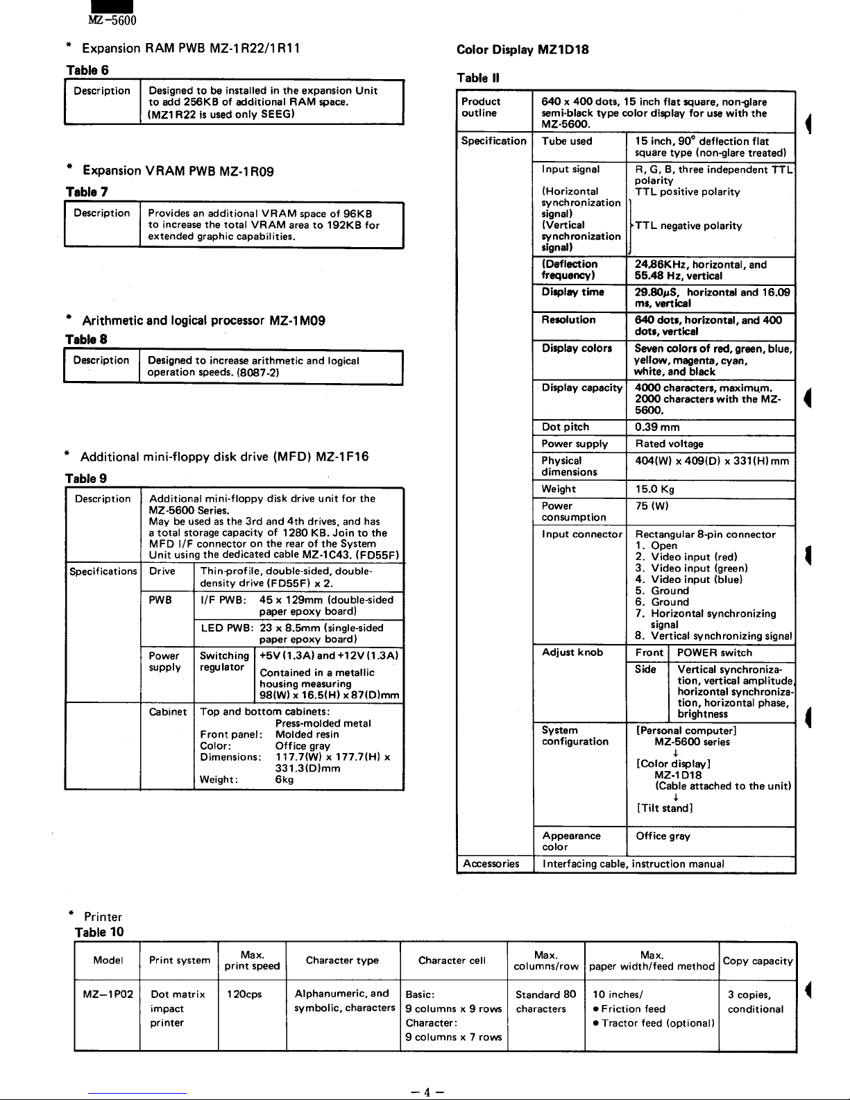
MZ1D18
Table
11
Product
640 x 400
dots,
15
inch
flat
square, non-glare
outline
semi-black
type
color
display
for
use
with
the
MZ-5600.
Specification
Tube used
15
inch,
90°
deflection
flat
square
type
(non-glare treated)
I
nput
signal
R, G, B, three independent
TTL
polarity
(Horizontal
TTL
positive
polarity
synchro.nization
}
TIL
"'9";W
pol,d",
signal)
(Vertical
synchronization
signal)
(Deflection
24.86KHz,
horizontal,
and
frequency)
55.48
Hz,
vertical
Display
time
29.8O"S,
horizontal
and
16.09
ms, vertical
Resolution
640
dots,
horizontal,
and
400
dots,
vertical
Display
colors
Seven
colors
of
red, green, blue,
yellow,
magenta, cyan,
white,
and black
Display capacity
4000
characters,
maximllm.
2000
characters
with
the
MZ-
5600.
Dot
pitch
0.39
mm
Power supply
Rated voltage
Physical
404(W) x
409(0) x 331(H)
mm
dimensions
Weight
15.0 Kg
Power
75 (W)
consumption
I
nput
connector
Rectangular
8-pin
connector
1. Open
2.
Video
input
(red)
3.
Video
input
(green)
4.
Video
input
(blue)
5.
Ground
6.
Ground
7.
Horizontal
synchronizing
signal
8.
Vertical
synchronizing signal
Adjust
knob
Front
POWER switch
Side
Vertical
synchroniza·
tion,
vertical
amplitude
horizontal
synchroniza-
tion,
horizontal
phase,
brightness
System
[Personal
computer]
configuration
MZ-56oo
series
.j.
[Color
display]
MZ-1D18
(Cable attached
to
the
unit)
.j.
[Tilt
stand]
Appearance
Office
gray
color
Accessories
I nterfacing cable,
instruction
manual
Character cell
Max. Max.
Copy capacity
columns/row
paper
width/feed
method
Basic: Standard
80
10
inches/
3 copies,
9 columns x 9 rows characters
•
Friction
feed
conditional
Character: •
Tractor
feed
(optional)
9 columns x 7 rows
-4-
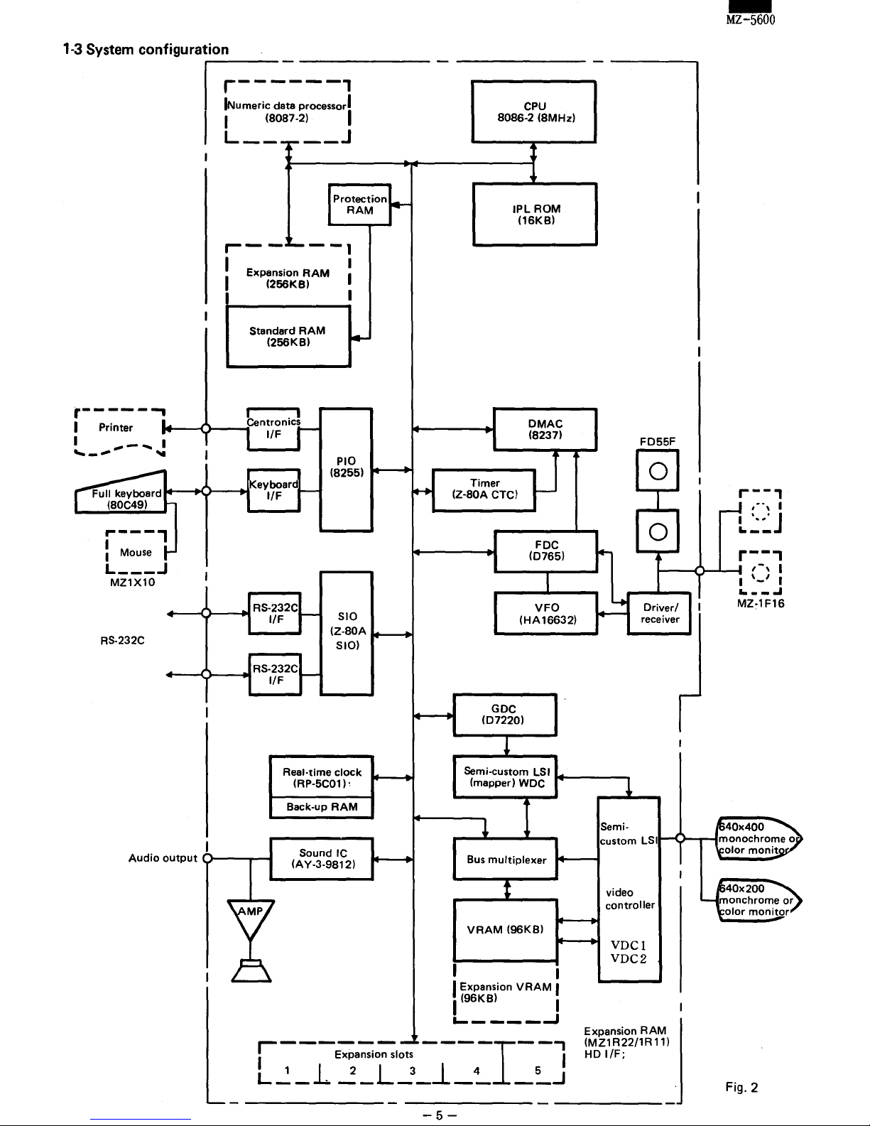
1-3
System configuration
r------,
Printer
.------
r------,
INumeric
data processorl
I (SOS7-2) I
L
____
J
Protection
RAM
r--
--1
11
Expansion
RAM
1I
(256KB)
I
Standard
RAM
(256KB)
PlO
(8255)
..--~
....
-II>O>---i~.
eyboard
IIF
,..---,
I
I Mouse
L
___
J
MZ1X10
RS-232C
+-_Q-_-""
RS-232C
IIF
+--0--"""
RS-232C
IIF
SIO
(Z-80A
....
_+I
510)
CPU
SOS6-2
(SMHz)
IPL
ROM
(16KB)
Timer
(Z-SOA CTC)
GDC
(07220)
DMAC
(8237)
FD55F
o
o
Driverl
receiver
Real-time
clock
(RP-5C01 ),
Semi-custom LSI
M-----.
(mapper) WDC
Audio
output
D---r--
....
Back-up
RAM
Sound IC
(AY-3-9812)
Bus
multiplexer
VRAM
(96KB)
I
I Expansion
VRAM
I
I
(96KB)
I
L..
____
-'
i---~a-:o::lots
----r--
1
1
1.2L3
14
5
L
__
.
__
__...L__
__.J
-5-
Semi-
custom
LSIt-O"""T-f
video
controller
VDCl
VDC2
Expansion
RAM
1
(MZ1R22/1R11)
HO
I/F;
-
MZ-5600
r--,
t
-',
I
I
•••.
J
'---
r--'
I , I
I
'-'
I
"---'
MZ:1F16
Fig. 2
-
MZ-5600
2.
SOFTWARE CONFIGURATION
1.
2.
8.
2-1
System bootstrap
It
becomes possible with
the
MZ-5600
to
bootstrap from
the
hard disk when
the
CPM.SYS or
MSOOS
is
stored
on
the
hard disk, provided
that
the
following restriction
is
applicable.
"The
system file (CPM.SYS
or
MS
DOS) can only be loaded
from
the
physical drive unit number 0 during IPL."
If
the CPM.SYS has been stored in
the
HOO,
for instance;
Disk
not
inserted in +
the drive
A.
Drive A
0
+
CPM.SYS
Drive A
0
+
MSDOS
CPM.SY
S
CPM.SY
t3
POWER
ON
Bootstrapped
with
....::..:..:......-
.......
the
CPM.SYS
from
the HDO.
POWER
Bootstrapped
with
ON
•
the
CPM.SYS
from
the
drive
A.
POWER
ON
Bootstrapped
with
..
the
MSDOS
on
the drive
A.
Thus, it becomes necessary
to
store
the
MSOOS after erasing
the
CPM.SYS on
the
HOO,
inorder
to
bootstrap
the
MSOOS
from the hard disk.
SYSTEM DISK
DEVICE
SYSTEM
DISK
640KB
MFD
0
HD
0
320KB
MFD
X
SFD
X
640KB
MFO
format
256 bytes/sector
16 sectors/track
80
tracks/side
Must be created
by
DSKMAINT.
Must be created
by
DSKMAINT.
Creation and bootstrap are
not
possible.
Creation and bootstrap are
not
possible.
2K bytes/block
128 directory entries
* Prior to
the
use
of
a fresh disk, it becomes necessary
to
format
the
disk using OSKMAINT.
2-2 CP/M-86
Logical drive map
Logical drive A
j B
C
I
D E
I
FIG
I
640KB
MFD
SFD
1
Physical drive
0
I 1 2 I
3
0
I 1 I 2 I
HD
1f
if
2
Physical drive
0
1)
Setup for above 1
or 2 is
possible using IOCNF utility
program.
2) M represents
the
memory disk.
3) N supports the
SFOO
of
the
one·sided, single denSity.
H
3
-6-
I
I
J
K I L
M N
0
HD
N.U
MD
SFD
320KB
MFD
C
1
0
0
O~3
if
if
if
4) 0 supports
MFOO·3
as
320/640
KB
MFO. For kind
of
the
disk supported, refer
to
instruction book, OSKCNV.
But drive 0 can only be read.
If
write
is
tried
to a 320
KB
disk, it
evoke-s a BOOS
error.
,
o : 0
40
: 0
40 : 2600
x:o
Cl)
Q
ID
INT
VECTOR
TABLE
CCP
11
BOOS
[9K]
Interface block
[5K]
IOCS
code
block
[27K]
---------
-
.....
--
..............
-::..
.....................
--
IOes
data
block
[SKI
Y:o
...
TPA
~lo!
.~
z:J~_---IJ
Standard CP/M-86
Fig. 3
The
above
figure provides the memory map
for
the ep/M-
86
used
on
the MZ-5600.
The
BIOS
consists
of
the following three blocks:
i) Interface block: Interfaces the
BOOS
with
loes.
ii)
loes
code
block: Control program
for
the input
output
device handler called the
Input Output Control System
(lOeS).
iii)
loes
data block: Parameter
and
work
area
used
~
for
the
loes.
The
MZ-5600 system
can
be
upgraded by using
an
IN-
STALL
command which integrates the optional
loes
module into the BIOS.
The
above
figure on the right
provides
the memory map
for
the upgraded system:
...
-
l~
-7-
Additional IOes
code
Additional IOes
data
I~
Fig.4
-
MZ-5600
OOOH
Type 0
Vector
Type 1
Vector
~~
080H
Type
32
Vector
::~
100H
Type
64
Vector
Type
80
Vector
:::=
168H
Type
90
Vector
~:::
380H
Type
224
Vector
::~
3F4H
Type
253
Vector
3F8H
Type
254
Vector
Type
255
Vector
400H
CP/M-B6 transient command
set
ASMB6: Assembler
for
the
BOB6
GENCMD: Command file production
utility
DDTB6:
ED:
PIP:
STAT:
SUBMIT:
HELP:
DSKMAINT
Dynamic debugging tool
Editor
File merge and transfer
utility
File and disk status display
utility
Batch processing
utility
Command
usage
display
utility
FORMAT
COPYDISK
COPYFILE
COPYSYS
VERIFY
*
~.
~
~
==
*
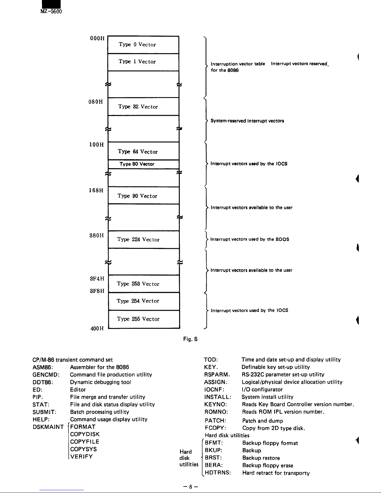
Fig. 5
Interruption vector table Interrupt vectors reserved.
for the
8086
System-reserved interrupt vectors
Interrupt vectors used
by
the IDeS
. Interrupt vectors availeble
to
the user
}
Interrupt vectors used
by
the
BOOS
Interrupt vectors available
to
the user
Interrupt vectors used
by
the IDeS
TOD:
KEY.
RSPARM.
Time and date set-up and
display
utility
Definable key set-up
utility
RS-232C parameter set-up
utility
ASSIGN: Logical/physical device allocation
utility
10CN F:
I/O
configurator
INSTALL:
System install
utility
KEYNO:
Reads
Key Board Controller version number.
ROMNO:
Reads
ROM IPL version number.
PATCH: Patch and dump
FCOPY: Copy from 2D type disk.
Hard disk
utilities
Hard BKUP: Backup
[
BFMT: Backup
floppy
format
disk
BRST: Backup restore
utilities
BE
RA: Backup
floppy
erase
HDTRNS: Hard retract
for
transporty
-8-
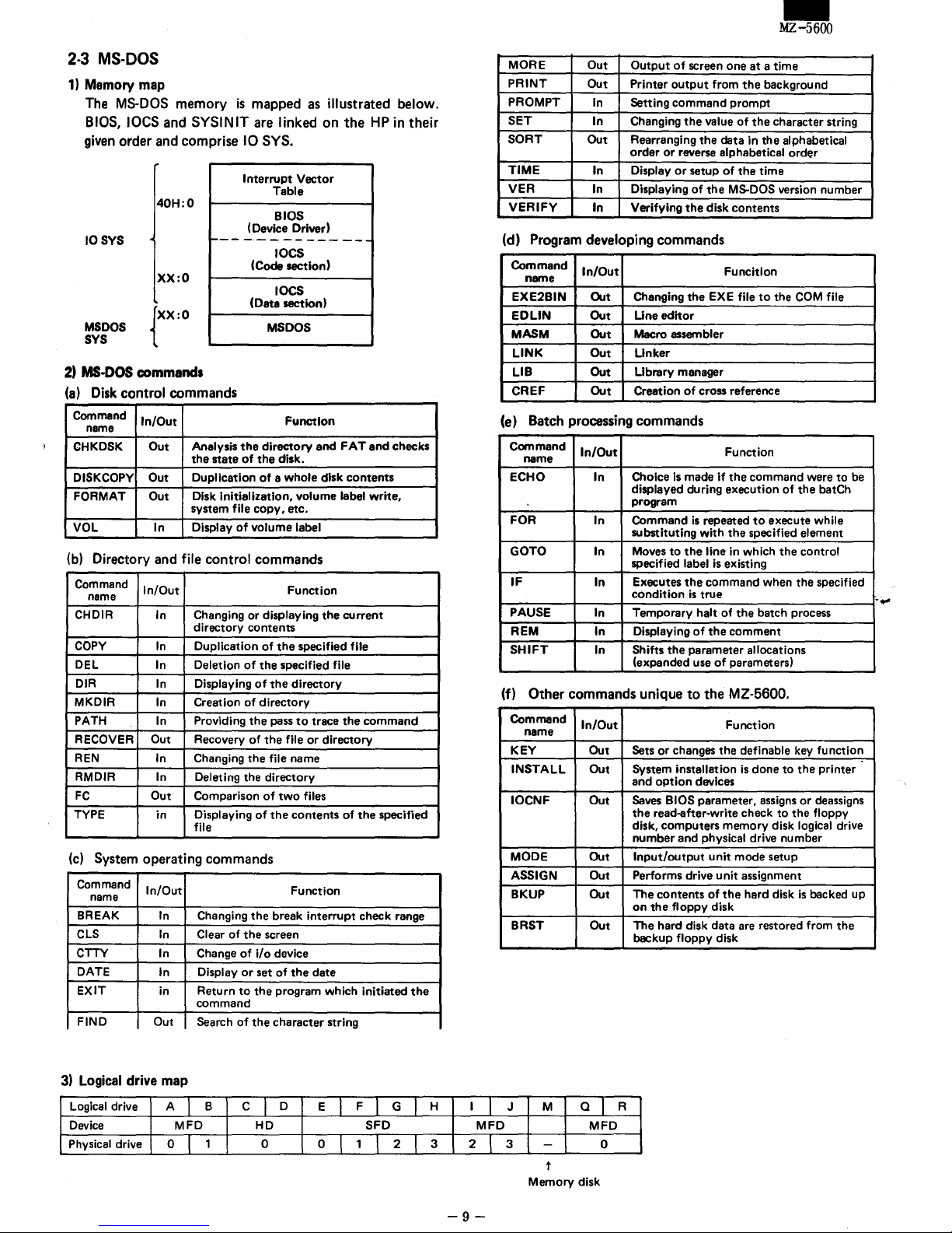
2-3
MS-DOS
1)
Memory
map
The
MS-DOS
memory
is
mapped
as
illustrated below.
BIOS,
IDeS
and
SYSINIT
are
linked on the
HP
in their
given
order
and
comprise 10 SYS.
Interrupt
Vector
Table
40H:O
BIOS
(Device Driverl
10SYS
r---
-.----
-----
IOes
(Code section)
xx:o
loeS
MSDOS
t
x
:
o
SYS
(Data section)
MSDOS
2)
MS-DOS
commands
(a)
Disk control commands
Command
In/Out
Function
name
CHKDSK
Out
Analysis
the
directory
and
FAT
and
checks
the
state
of
the
disk.
DISKCOPY Out
Duplication
of
a whole disk
contents
FORMAT Out
Disk initialization. volume label write.
system file
copy.
etc.
VOl
In
Display
of
volume label
(b)
Directory
and
file control commands
Command
In/Out Function
name
CHDIR
In
Changing or displaying
the
current
directory
contents
COpy
In
Duplication
of
the
specified file
DEL
In
Deletion
of
the
specified file
DIR
In
Displaying
of
the
directory
MKDIR
In
Creation of
directory
PATH
In
Providing
the
pass
to
trace
the
command
RECOVER Out
Recovery of
the
file
or
directory
REN
In
Changing
the
file name
RMDIR
In
Deleting
the
directory
FC
Out
Comparison
of
two
files
TYPE in Displaying
of
the
contents
of
the
specified
file
(c)
System
operating commands
Command
In/Out Function
name
BREAK
In
Changing
the
break interrupt check range
ClS
In
Clear of
the
screen
CTTY
In
Change
of
i/o
device
DATE
In
Display
or
set
of
the
date
EXIT
in
Return
to
the
program which initiated
the
command
FIND
Out
Search
of
the
character string
3)
Logical drive map
logical drive
A
I
B
CiD
E
I
F I
G I
H
Device
MFD
HD
SFD
Physical drive
o 1
1
0 0
I
1
I 2 I
3
-
MZ-5600
MORE
Out
Output
of
screen
one
at a time
PRINT
Out
Printer
output
from
the
background
PROMPT
In
Setting
command
prompt
SET
In
Changing
the
value of
the
character string
SORT
Out
Rearranging
the
data
in
the
alphabetical
order
or
reverse alphabetical order
TIME
In
Display
or
setup
of
the
time
VER
In
Displaying
of
the
MS-DOS version number
VERIFY
In
Verifying
the
disk
contents
(d) Program developing commands
Command
In/Out
Funcition
name
EXE2BIN Out
Changing
the
EXE file
to
the
COM
file
EDLlN
Out
Uneeditor
MASM
Out
Macro assembler
LINK
Out
Llnker
LIB
Out
Library manager
CREF
Out
Creation
of
cross reference
(e) Batch processing commands
Command
In/Out
Function
name
ECHO
In
Choice
Is
made if
the
command
were
to
be
displayed during execution of
the
batCh
program
FOR In Command
is
repeated
to
execute while
substituting with
the
specified element
GOTO
In
Moves
to
the
line in which
the
control
specified label
is
existing
IF
In
Executes
the
command
when
the
specified
condition
is
true
.
PAUSE
In
Temporary halt of
the
batch process
REM
In
Displaying
of
the
comment
SHIFT
In
Shifts
the
parameter allocations
(expanded use
of
parameters)
(f)
Other commands unique
to
the MZ-5600.
Command
In/Out
Function
name
KEY
Out Sets or changes
the
definable key function
INSTALL Out System installation
is
done
to
the
printer
and
option
devices
10CNF Out Saves BIOS parameter. assigns
or
deassigns
the
read-after-write check
to
the
floppy
disk.
computers
memory disk logical drive
number
and
physical drive number
MODE
Out
Input/output
unit
mode
setup
ASSIGN Out Performs drive
unit
assignment
BKUP
Out The
contents
of
the
hard disk
is
backed up
on
the
floppy disk
BRST Out The hard disk
data
are restored from
the
beckup floppy disk
I I
J M
Q I R
MFD MFD
2 I
3 -
0
t
Memory disk
-9-
-
MZ-5600
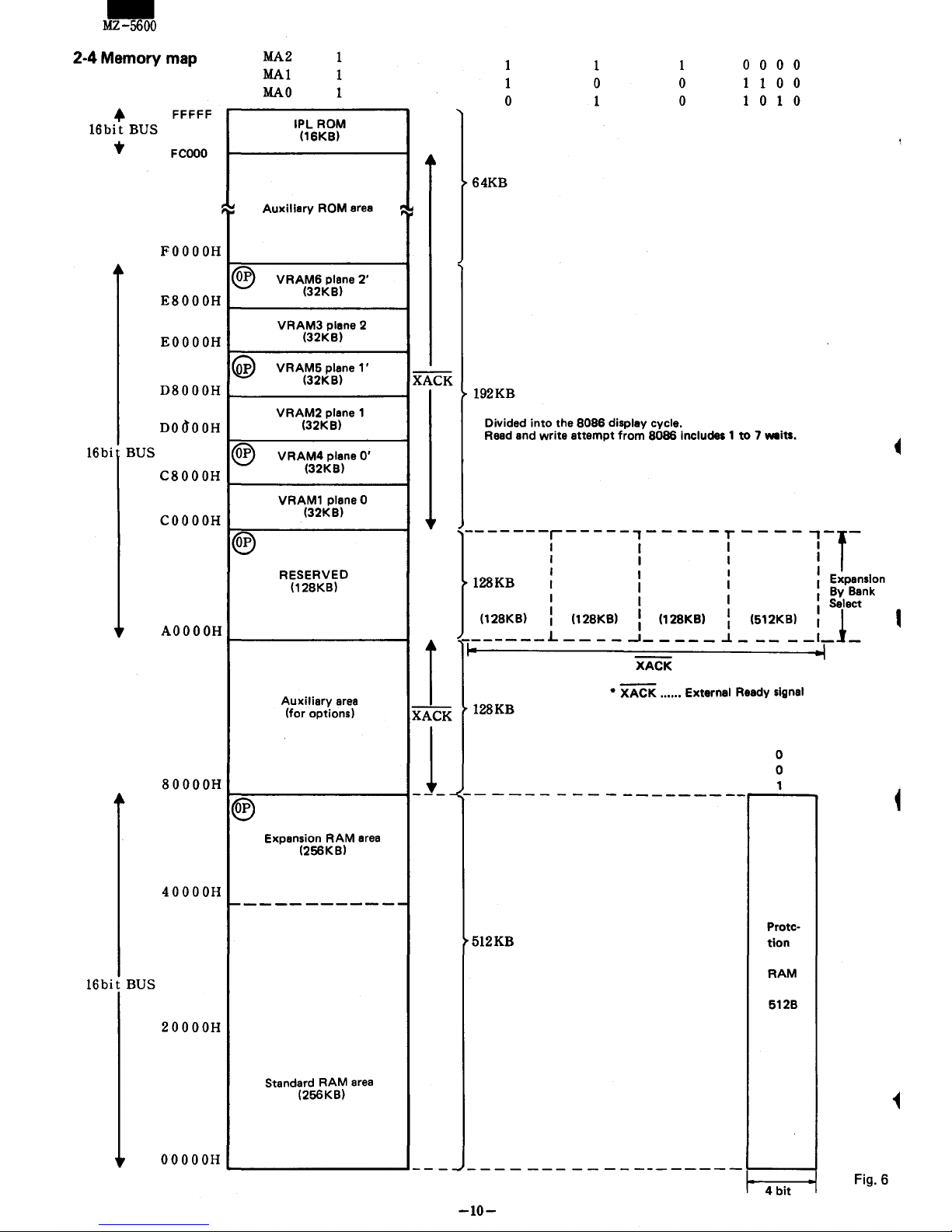
2-4 Memory map
+
16bit
BUS
...
FFFFF
FCOOO
FOOOOH
E8000H
EOOOOH
D8000H
DodoOH
16bi BUS
C8000H
COOOOH
~~
®
~
®
®
AOOOOH
80000
H
®
40000
H
MA2
MAl
MAO
1
1
1
IPL ROM
(16KB)
Auxiliary
ROM
area
VRAM6
plane
2'
(32KB)
VRAM3
plane 2
(32KB)
VRAM6
plane
l'
(32KB)
VRAM2
plane 1
(32KB)
VRAM4
plane
0'
(32KB)
VRAM1
plane 0
(32KB)
RESERVED
(128KB)
Auxiliary
area
(for options)
Expansion
RAM
area
(266KB)
,
~~
X
ACK
1
1
o
64KB
192KB
1
o
1
1
o
o
Divided
into
the 8086 display cycle.
o 0 0 0
1
100
1
010
Read
and write attempt
from
8086 Includes 1
to
7
Mits.
-------:------1-
----r ---
-1-,-
128KB
I I : : Expansion
I I By Bank
I I I : Select
(128KB)
: (128KB) : (128KB) I (612KB) I i
_______
L
____
-'
_____
...1 _____ 1 __
I-
~
XACK
•
XAcK
......
External Raady signal
1
XACK 128KB
1
~--
-
--
-----
---------r--------o.~
------------
16bit
BUS
20000
H
Standard
RAM
area
(266KB)
00000
H
512KB
Protction
RAM
612B
-
-~
---
-
---
- -
--
--------1-----1
4
bit
-10-
Fig.6
,
Set up
8086's
VOC1,
WOC
and GOC.
Fig. 7
REFRESH
START
-11-
-
MZ-5600
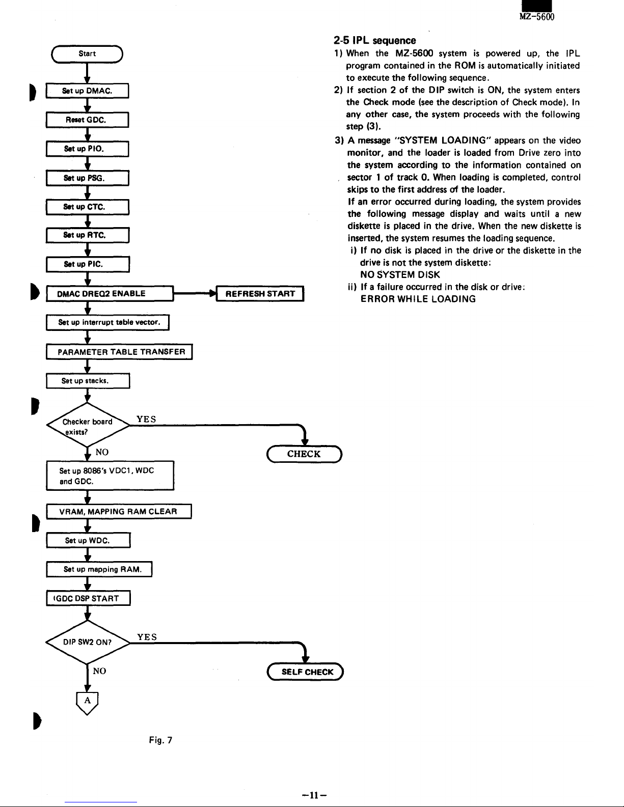
2-51PL sequence
1) When
the
MZ-5600 system
is
powered up, the
IPL
program contained
in
the
ROM
is
automatically initiated
to
execute
the
following sequence.
2)
If
section 2
of
the
DIP switch
is
ON, the system enters
the
Check mode (see
the
description
of
Check mode).
In
any
other
case,
the
system proceeds with
the
following
step
(3).
3)
A message "SYSTEM LOADING" appears on
the
video
monitor, and
the
loader
is
loaded from Drive zero into
the
system according
to
the
information contained on
sector
1
of
track
O.
When loading
is
completed, control
skips
to
the
first address
at
the
loader.
If
an error occurred during loading,
the
system provides
the
following message display and waits until a new
diskette
is
placed
in
the
drive.
When
the
new diskette
is
inserted,
the
system resumes
the
loading sequence.
i)
If
no
disk
is
placed in
the
drive
or
the
diskette
in
the
drive
is
not
the
system diskette:
NO
SYSTEM DISK
ii)
If
a failure occurred
in
the
disk
or
drive:
ERROR WHILE LOADING
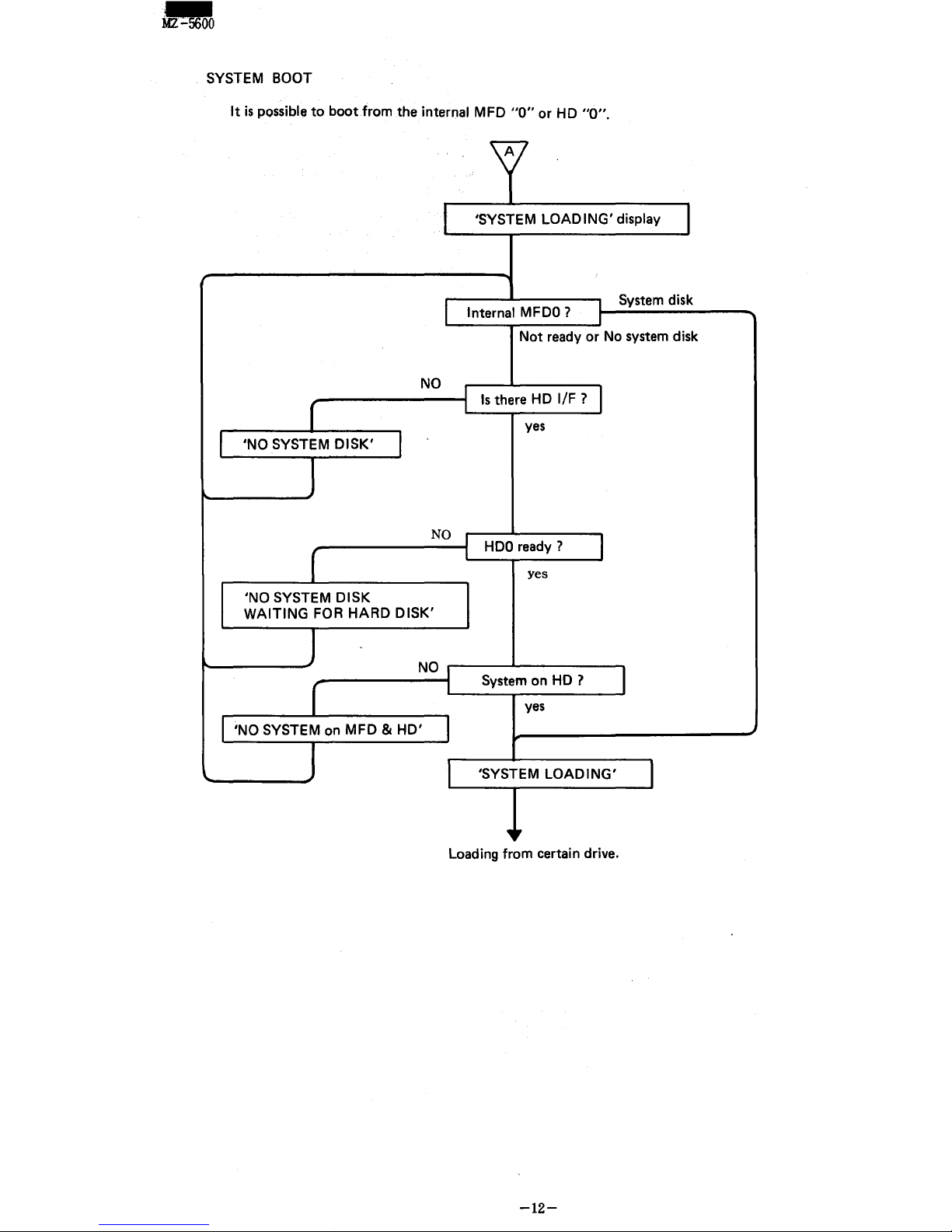
MZ-5600
SYSTEM BOOT
It
is
possible
to
boot from the internal MFD
"0"
or HD
"0".
r
I
'SYSTEM LOADING' display
I
System
disk
I
Internal
MFDO
?
I
Not
ready or No
system
disk
NO
I
Is
there HD
I/F?
I
r
I
yes
'NO SYSTEM
DISK'
I
J
NO
I
I
f
I
HDO
ready?
yes
'NO SYSTEM DISK
WAITING FOR
HARD DISK'
J
NO
I
System on HD ?
I
r
I
yes
'NO SYSTEM
on
MFD &
HD'
I
J
I
'SYSTEM LOADING'
I
~Ir
Loading from certain drive.
-12-
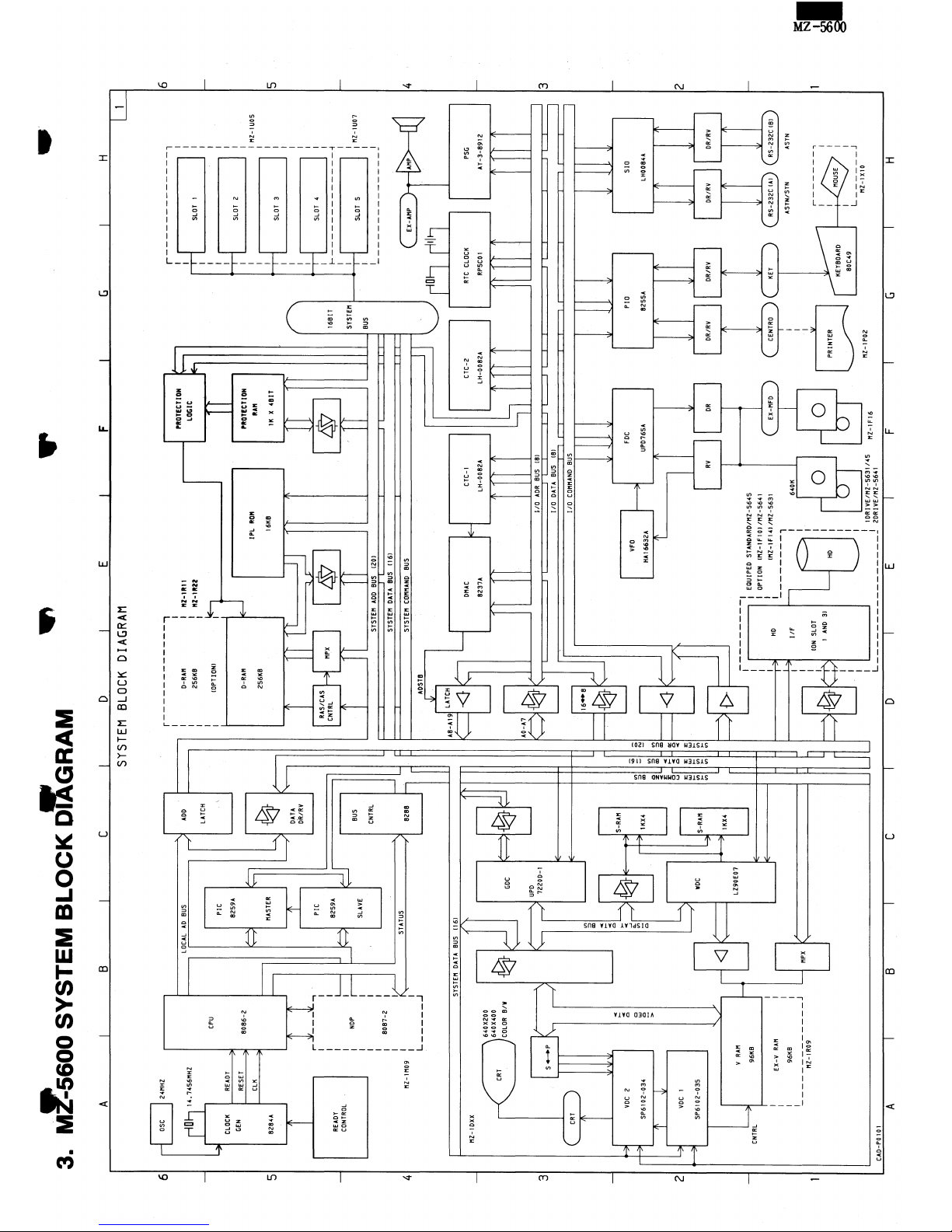
3.
M!5600
SYSTEM BLOCK
01rGRAM
~
~
-
A
I
B
I
C
I D
I E I
F
I
G
I
H
SYSTEM
BLOCK
DIAGRAM
LL
61
8"MHZ
.-----
-
4
5
-
4
-
3
14.745611HZ
•
CLOCK
GEN
8284A
T
READT
CONTROL
READY
RESET
CLK
I'1Z-11'109
I---
CPU
8086-2
h
rl--L
I
LOCAL
AD
BUS
.-----
PlC
825911
~
MASTER
PlC
NDP
I L-I
,---
~
8259"
I
SLAVE
I
I
'---
8087-2
I
K
STATUS
I
L
_____
.J
SYSTEM
DATA
BUS
1161
r
'DD
I--
LATCH
L---
~
~
~
OR/RV
L---
.---
BUS
~
CNTRL
~r
I'1Z-1DXX
t0
640X200
640X400
CRT
COLOR
B/W
~
.----
~p
~UPD
l...---
72200-1
r
I'<-
S
4-+P
,-------I
~
L---
.--
L--
~
~
t J
vac
2
SP6102-034
~~~',::
L--
L--
0;
~
m
21
-
I
:
EX-V
RAM
I
I
96KB :
,
_____________
J
I'1Z-1 R09
CAD-PO
101
A I
LS[I
LZ90E07
.--
L---.J
\inllll'l
1 KX4
~
MP'
~~,
________________
~
~
"Ir
!
IU
B
I C I
r------------.,
, I
I O-RAM I
: 256MB :
,
, (OPTION)
111-1ltl1
"Z-1
RZZ
Q-RAM
w
256MB
IPL
ROI'I
16MB
'"onCTION
.,.
I"
x "BIT
r-------------l
I I
r+l
SLDT
I i
I I
~
SlOT 2 i
I I 1'11-1
uos
, I
I I
SLOT 3 I
I
I , I
SLOT"
I
I ,
16BIT
I---~-------------l
I I
SYSTEM
I I
SLOT
5 I
MZ-1U07
'--'-Ll-j
BUS
I :
ADSTB
,£
~~H~
L--...J
SYSTEM
DATA
BUS
(16)
SYSTEM
COMAND
BUS
OMAC
8237A
VFO
HA
16632A
,
CTC-l
LH-0082A
"U
UI'.'I'.
BUS
181
1/0
COMMAND
BUS
111
FOC
UPOi65A
w:
r'
}Lm:
""".
"
......
,""
'----,:_-_-_.J
__
~
I I OPTION
lMZ-lfl01/t1Z-5641
~------;IPI
HO
1
lt1Z-lf141/MZ
5631
---------------
1II1
11
1
I-m
--------;
I
ASTN/STN
ASTN
I/f
I
: I
ION
SlOT I
[3]
1
AND
31
I
I
PRINTER
I
I
I I
L
________________
J
~~:!~~~~i=;~!:/45
MZ-1F16
MZ-1P02
D
I
E
I F I
G
I
H
6
I-
5
I-
4
3
-
2
f-
~I
•
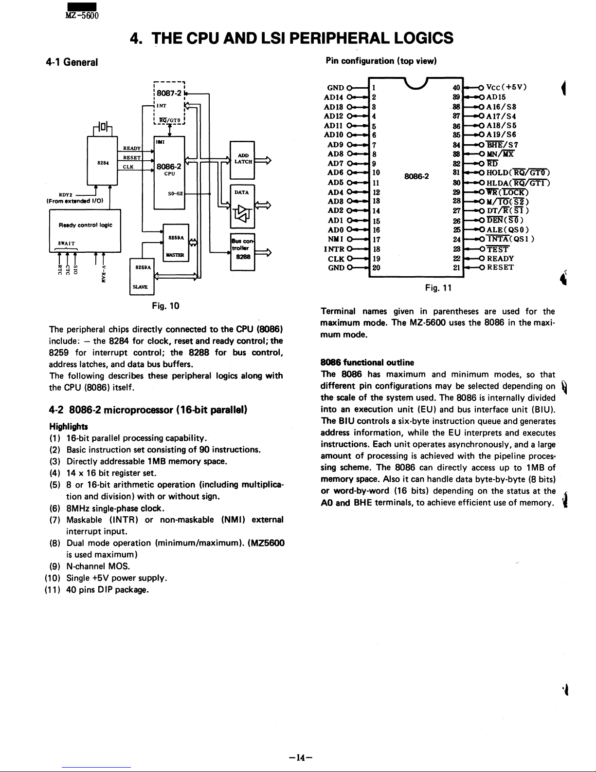
4. THE CPU
ANDLSI
PERIPHERAL LOGICS
4·'
General
[)
8284
Reedy cOntrol logic
aWA'T
READY
RESET
CLK
-----,
, ,
:8087-2
I I
"NT
...
,
CPU
SIH>2
Fig. 10
The
peripheral chips directly connected
to
the
CPU
(8086)
include: - the 8284
for
clock, reset and ready control; the
8259 for interrupt
control; the 8288
for
bus
control,
address
latches,
and
data
bus
buffers.
The
following describes
these
peripheral logics along
with
the
CPU
(8086) itself.
4·2 8086·2 microprocessor (16-bit parallel)
Highlights
(1) 16-bit parallel processing capability.
(2)
Basic
instruction
set
consisting
of
90
instructions.
(3)
Directly
addressable
1 MB memory
space.
(4)
14 x 16
bit
register
set.
(5)
8 or 16-bit arithmetic operation (including multiplication
and
division)
with
or
without
sign.
(6) 8MHz
single-phase
clock.
(7)
Maskable
(lNTR)
or
non-maskable (NMI) external
interrupt input.
(8)
Dual
mode operation (minimum/maximum). (MZ5600
is
used
maximum)
(9)
N-channel
MOS.
(10) Single +5V power supply.
(11) 40 pins DIP package.
-14-
Pin configuration
(top
view)
GND
.
Vcc(+5V)
~
ADl"
.
ADl5
AD
18
A16/S8
ADl2
AI7/S"
AD
11
A18/S5
AD
10
A19/S6
AD9
'BiIE/S7
AD8
IINIJiX
AD7
m
AD6
8086-2
HOLD(RQ/GR)
AD5
HLDA(RQ/GTI
)
AD"
lrIf('IOO()
AD8
1I/iO(Sf)
AD2
DT/1f(ST
)
ADI
IiEN(Sli)
ADO
ALE(QSO)
NIl I
INTA(QSl)
INTR
TEST
eLK
READY
GND
RESET
Fig.
11
,
Terminal
names
given in
parentheses
are
used
for
the
maximum mode. The
MZ-5600
uses
the 8086 in the maxi-
mum mode.
8086 functional outline
The 8086
has
maximum
and
minimum modes,
so
that
different pin configurations may
be
selected depending
on
~
the·
scale
of
the system
used.
The 8086
is
internally divided
into
an
execution
unit
(EU)
and
bus
interface
unit
(BIU).
The BIU controls a six-byte instruction queue
and
generates
address
information, while the
EU
interprets
and
executes
instructions.
Each
unit
operates asynchronously,
and a large
amount
of
processing
is
achieved with the pipeline
proces!,
sing
scheme.
The 8086
can
directly
access
up
to
1 MB
of
memory
space.
Also
it
can
handle data byte-by-byte (8 bits)
or
word-by-word (16 bits) depending on the status at the
AO
and
BHE terminals,
to
achieve
efficient
use
of
memory.
~
....
C1I
I
Block
diagram
~------------~
~~----------------------~--------~
Address
bus
or
bidirectionel
data bus
BHE/S7~
AD
18
AD
12
AD
11
Interrupt
acknowledge ( I
NfA)
Write
control
(n')
Read
control
Data transfer
control
Data send/receive
(DT
IR)
control
__
Data enable
DEN
Address latch enable
(ALE)
8
Address adder ( B I U )
os
(16)
ss
(16)
ES
(16)
I Segment register/
I P
(16)
Instruction
pointer
.6-byte
-'-,;..;..---f
l
instruction
>
~
0 )
Quaue
buffer
.
1
t
I
Timing
status
-------'-I------------r----...J-f------:r---:r-......:-.-j~.
and
control
'f
logic
16
16
16
1------
16
_L
J_
~
- -
--
AH
(8)
AL
(8)
BH
(8)
BL
(8)
CH
(8)
CL
(8)
DH
(8)
DL
(8,)
SP
(I6
)
BP
(I6
)
SI
(I6
)
DI
(I6
)
General-purpose
register
file
Parallel 16-bit
I logical
unit
Execution
unit
(EUI
Fig. 12
INTR
Maskable
interrupt
request
input
Non-masklble
interrupt
Reset
input
request
input
~
READY Ready
input
1---(23)
TEST
Test
input
RQ IGTO} Request grant
:3Q)
RQ
IGTI
output
(MaxI
1)
,(
HOLD)
Hold
request
input
(MinI
(HLDA)
Hold acknowledge
output
CLK
~MN/MX
~~
P--(28)S2
Clock
input
(MinI
Mode select
input
Lock
request
output
(MaxI
} Queue status
output
(MaxI
}
"'M
00""'
IM'"
;1
Pin
functions
Pins
having the
same
function in both Max. and Min.
modes.
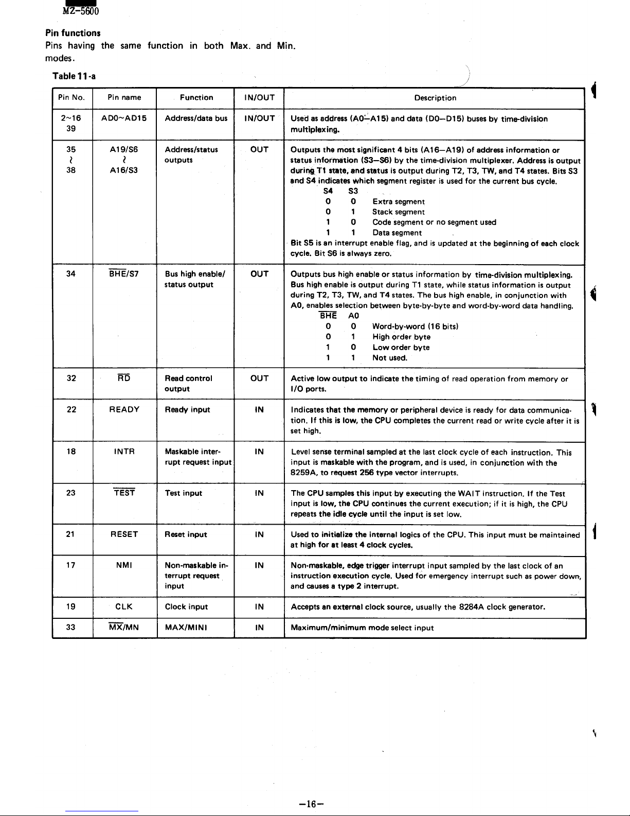
Table 11-a
)
Pin No. Pin name
Function
IN/OUT
Description
2-16
ADO-AD15
Address/data bus
IN/OUT
Used
as
address (AO:':'A
15)
and data
(00-015)
buses
by
time-division
39
multiplexing.
35
A19/56
Address/status
OUT
Outputs
the
most
significant 4 bits
(A16-A19)
of
address
information
or
l
l
outputs
status
information
(53-56)
by
the
time-division
multiplexer.
Address
is
output
38
A16/53
during
T1
state,
and
status
is
output
during
T2,
T3,
TW,
and
T4
states. Bits
53
and
54
indicates
which
segment register
is
used
for
the
current
bus cycle.
54
53
0 0
Extra
segment
0 1
5tack
segment
1
0
Code segment
or
no segment used
1 1 Data segment
Bit
55
is
an
interrupt
enable flag, and
is
updated
at
the beginning
of
each
clock
cycle.
Bit
56
is
always zero.
34
BHE/57
Bus
high enable/
OUT
Outputs
bus high enable
or
status
information
by
time-division
multiplexing.
status
output
Bus high enable
is
output
during
Tl
state,
while
status
information
is
output
during
T2,
T3, TW, and
T4
states. The bus high enable, in
conjunction
with
AO, enables selection between
byte·by-byte
and
word·by-word
data handling.
BHE
AO
0 0
Word-by-word
(16 bits)
0 1 High
order
byte
1 0
Low
order
byte
1 1
Not
used.
32
RD
Read
control
OUT
Active
low
output
to
indicate
the
timing
of
read operation
from
memory
or
output
I/O
ports.
22
READY
Ready
input
IN
Indicates
that
the
memory
or
peripheral device
is
ready
for
data communica·
tion.
If
this
is
low,
the
CPU completes
the
current
read
or
write
cycle
after
it
is
set high.
18
INTR
Maskable inter-
IN
level
sense
terminal
sampled
at
the
last
clock
cycle
of
each
instruction.
This
rupt
request
input
input
is
maskable
with
the
program, and
is
used, in
conjunction
with
the
8259A,
to
request
256
type
vector interrupts.
23
TE5T
Test
input
IN
The CPU samples
this
input
tly
executing the
WAIT
instruction.
If
the Test
input
is
low,
the
CPU continues
the
current
execution;
if it
is
high, the CPU
repeats
the
idle
cycle
until
the
input
is
set low.
21
RE5ET
Reset
input
IN
Used
to
initialize
the
internal
logics
of
the CPU. This
input
must
be maintained
at
high
for
at
least 4
clock
cycles.
17
NMI
Non-maskable in-
IN
Non-maskable, edge trigger
interrupt
input
sampled
by
the last
clock
of
an
terrupt
request
instruction
execution
cycle. Used
for
emergency
interrupt
such
as
power
down,
input
and
causes a type 2 interrupt.
-
..
19
ClK
Clock
input
IN
Accepts an external
clock
source, usually
the
8284A
clock
generator.
33
MX/MN
MAX/MINI
IN
Maximum/minimum
mode
select
input
-16-
Pin
used
for
minimum
mode.
-lIviwl".
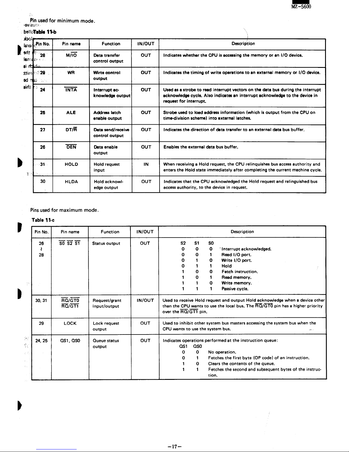
bel!oTable
11
..
b
,j:)O
l.
t:
s.
k!inNo.
Pin name
Function
1
,.
28
M/la
Deta
tra
nsfer
t
"n
ai
1
p"
ri-
,-{"
111
",':'29
ui
ad
tiff
!1
'.
, "
1
24
25
27
26
31
('
I
30
control
output
WR
Wirte
control
output
1NTA
Interrupt
ac-
knowledge
output
ALE
Address
latch
enable
output
DT/R
Deta send/receive
control
output
DEN
Data enable
output
HOLD
Hold
request
input
HLDA Hold acknowl·
edge
output
Pins
used
for
maximum mode.
Table 11·c
Pin
No.
Pin
name
Function
26
SOS251
Status
output
1
28
30,31
RQ/GTO
Request/grant
RQ/GT1
input/output
29
LOCK
Lock request
output
24,25
QS1,
QSO
Queue status
output
IN/OUT
OUT
OUT
OUT
OUT
OUT
OUT
IN
OUT
IN/OUT
OUT
IN/OUT
OUT
OUT
-
MZ-5600
Description
Indicates whether
the
CPU
is
accessing
the
memory or an
I/O
device.
Indicates
the
timing
of
write operations
to
an external memory or I/O device.
Used as a
strobe
to
read interrupt vectors
on
the
data
bus during
the
interrupt
acknowledge cycle. Also indicates an interrupt acknowledge
to
the
device
in
request
for
interrupt.
Strobe
used
to
load address information (which
is
output
from
the
CPU
on
time-division scheme)
into
external latches.
Indicates
the
direction
of
data transfer
to
an external data bus buffer.
Enables
the
external data bus buffer.
When receiving a
Hold request,
the
CPU
relinquishes bus access
authority
and
enters
the
Hold
state
immediately after completing
the
current
machine cycle.
Indicates
that
the
CPU acknowledged
the
Hold request
and
relinguished bus
access
authority,
to
the
device
in
request.
Description
S2
S1
SO
0 0 0
.
Interrupt
acknowledged.
0 0
1 Read I/O port.
0
1
0
Write I/O port.
0 1 1 Hold
1 0 0
Fetch instruction.
1
0
1 Read memory.
1 1
0
Write memory.
1 1 1
Passive
cycle.
Used
to
receive Hold request
and
output
Hold acknowledge when a device
other
than
the
CPU wants
to
use
the
local bus. The RQfGTO pin has a higher priority
over
the
RQfGT1 pin.
Used
to
inhibit
other
system bus masters accessing
the
system bus when
the
CPU
wants
to
use
the
system bus.
--
Indicates operations performed
at
the
instruction queue:
QS1
QSO
0 0
No
operation.
0
1
Fetches
the
first
byte
(OP
code) of an instruction.
1
0
Clears
the
contents of
the
queue.
1 1
Fetches
the
second and subsequent bytes of
the
instruc,
tion.
-17-
4-3 8284 clock generator and driver
Highlights
(1) Quartz-controlled oscillator with stable
output
fre-
quency.
(2) External clock input.
(3) capable
of
producing a reset signal upon power
on
when external resistors and capacitors are
ullCl_
Pin configuration
(top
view)
Clock oyne. Input
CSYNC_
...
rlpllor
..
·.loak
output
PCLK
_
Add_
..
l1li.
Input III
'IIRl"
_
RMCly
Input III
RDYI
-
'RMCIy
output
READY_
RMCly
Input
121
RDYI
-
Acid
...
_Ill.
Input
121
'DRT _
Cloak output
CLK
-
(OV)
GND
Fig.
13
Block
dlllram
_Vcc
(IV)
-XI
C/wIIII
....
'U
- XI
C/wIIII
/llllul1IJ
_'JnItP
.............
......
".'1 .........
......
_,~
CIIIII
....
......
...
Ole
. 0IIII
.....
1UIIIUt
.
~
'Ill'
,,-Input
_RBSET
"-toutput
Functional outline
The 8284
is
a clock generator and driver designed exclusive-
ly
for the 8086 processor. It contains a quartz-controlled
OICillator, frequency divider
(113)
to
create the clock
output,
frequency divider
(112)
to
produce the peripheral
~
clock outpUt (peLK), reset logic
to
synchronize with the
~
eLK, aod
ready
logic.
The
REI
Input accepts an external
.Ipl
that
I.
used
to
produce a
CPU
reset signal which
is
synchronous with 'the eLK
output,
and uses a Schmitt
-trigger circuit
In
Its
Input. A power-on reset signal can
be
procIaad
by
connecting a resistor and capacitor
to
this
mterml~
~-----------------------q«>----------------~D
F/e
EFl
Quartzcontrolled
OSC
4-4 8288 bus controller
Highlights
(1)
Outputs with a large number of fan-outs.
CKO
D
FFl
(2)
Advanced write control outputs
(AIOWC
and
AMWC)
Pin configuration
1/0 bus mode t:ontrol
input
lOB
......
C6V)
Ctock
input
eLK
......
Stlllu.input
ST
......
I
StICu'input
Frequency
divider
11/3)
SYNC
Fig.
14
Functional outline
CKO
Frequency
CKO
divider (1/2)
FF2
0
...
IInd/receiYe control
output
DT
/R
....
17
.....
MCE/"P'fiEli
Miln,,~.
e"lbl.
output/peripheral date
The 8288
is
a bus controller and driver used with the 8086
CPU
operating
in
the maximum mode. It decodes the
SO-S2
outputs from the
CPU
into command and control signals
and provides control signals for I/O devices and memory.
The 8288
is
usable
in
the multi-master configuration
in
which more than one master
CPU
is
attached
to
a single
data bus. The 8288 has
an
input pin
to
accept the control
signal
AEN
from the bus arbitor 8289.
Acktr
••
"tch
I"lble
output
ALE
....
Add,....
l".bI.
input
"'Am'..... 6
Memory
rud
control
output
lIROC'-
AdY.nc:ed
memory write control
output
AJIWC
+-
Memory write control outp,lt
~
4-
(DV)
GND
Fig.
15
D8t8
enlble
output
Comn.nd
e"_II.lnput
1/0 devic.
rud
control
output
Adwnced I/O
d",ice
writ.
control
output
I/O deviel write control
output
-18-
I
I
t
Clock Input
CLK
",
••
Input
Am
Cornrnend
.Mble
Input
CEN
I/O bul
macIt
_"'
«tput
lOB
,U'l"
:t2"!. j
PIn
functions
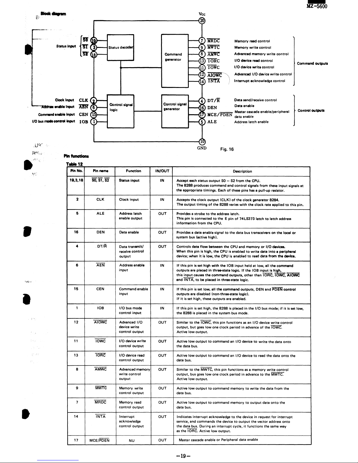
TIbIe'2
Pin
No.
19,3,18
2
S
16
4
6
15
1
12
11
13
8
9
7
14
17
Status
decoda
Control
signal
logic
Pin
name
Function
50,51,52
Status
input
ClK
Clock
input
ALE Address latch
enable
output
DEN Data enable
DT/R
Data
transmit/
receive control
output
AEN
Address enable
input
CEN
Command
enable
input
lOB
I/O
bus
mode
control
input
AIOWC Advanced I/O
device write
control
output
10WC
I/O
device
write
control
output
10RC
I/O device read
control
output
AMWC
Advanced
memory
write
control
output
MWTC
Memory write
control
output
MRDC Memory read
control
output
INTA
Interrupt
acknowledge
control
output
MCE/PDEN
NU
Vcc
MROC
MW'fC
Command
~
genarator
Memory read
control
Memory
write
control
Advanced
mamory
write
control
-
MZ-5600
lORC
I/O davice read
control
Command
outputs
IOWC
I/O device
write
control
AlOWC\
Advanced I/O device
write
control
mTA
Interrupt
acknowledge
control
DT/R
Data
send/receive
control
Data
enable
generator
DEN
/
-
__
Master cascade enable/peripheral
)lCE
PDEN
datll enable
ALE
Address latch eneble
GND
Fig. 16
IN/OUT
Description
IN
Accept
each
status
output
SO -52
from
the
CPU.
The
8288
produces
command
and
control
Signals
from
these
input
signals at
the
appropriate
timings. Each
of
these
pins
ha.
a pull-up resistor.
IN
Accepts
the
clock
output
(ClK)
of
the
clock generator
8284.
The
output
timing
of
the
8288
varies with
the
clock rate applied
to
this pin.
OUT
Provides a
strobe
to
the
address latch.
This pin
is
connected
to
the
E pin of
74lS373
latch
to
latch address
information from
the
CPU.
OUT
Provides a
data
enable signal
to
the
data
bus transceivers on
the
local
or
system bus (active high).
OUT
Controls
data
flow between
the
CPU
and
memory
or
I/O devices.
When this pin
i.
high,
the
CPU
is
enabled
to
write data
into
a peripheral
device; when it is
low,
the
CPU
is
enabled
to
read
data
from
the
device.
IN
If
this pin
is
set
high with
tha
lOB
input
held
at
low, all
the
command
outputs
are placed
in
three-.tate
logic.
If
the
lOB
input
is
high,
this
input
causes
the
command
outputs,
other
than
'i"5FiC,
10WC, AIOWC
and
INTA,
to
be pieced in
three-.tate
logic.
IN
If
this pin
is
set
low, all
the
command
outputs,
DEN
and
PO
EN
control
outputs
are disabled (non-three-state logic).
If
it
is
set high, these
outputs
are enabled.
IN
If
this pin
is
set high,
the
8288
is
placed
in
the
I/O bus
mode;
if it
is
sat low.
the
8288
is
placed
in
the
system bus mode.
OUT
Similar
to
the
10WC, this pin functions as an I/O device write
control
output,
but
goes
low
one
clock
period
in
advance
of
the
lowe.
Active
low
output.
OUT
Active low
output
to
command
an 1/0 device
to
write
the
data
onto
the
data
bus.
OUT
Active low
output
to
command
an
1/0
device
to
read
the
data
onto
the
data bus.
OUT
Similar
to
the
MWTC.
this pin functions as a memory write control
output,
bus goes low
one
clock period
in
advance
to
the
MWTC.
Active low
output.
OUT
Active low
output
to
command
memory
to
write
the
data from
the
data bus.
OUT
Active low
output
to
command
memory
to
output
data
onto
the
data bus.
OUT
Indicates
interrupt
acknowledge
to
the
device
in
request for
interrupt
service,
and
commands
the
device
to
output
the
vector address
onto
the
data
bus. Durirg an
interrupt
cycle, it functions
the
same way
as
the
10RC, Active low
output.
OUT
Master cascade enable or Peripheral data enable
-19-
-
MZ-5600
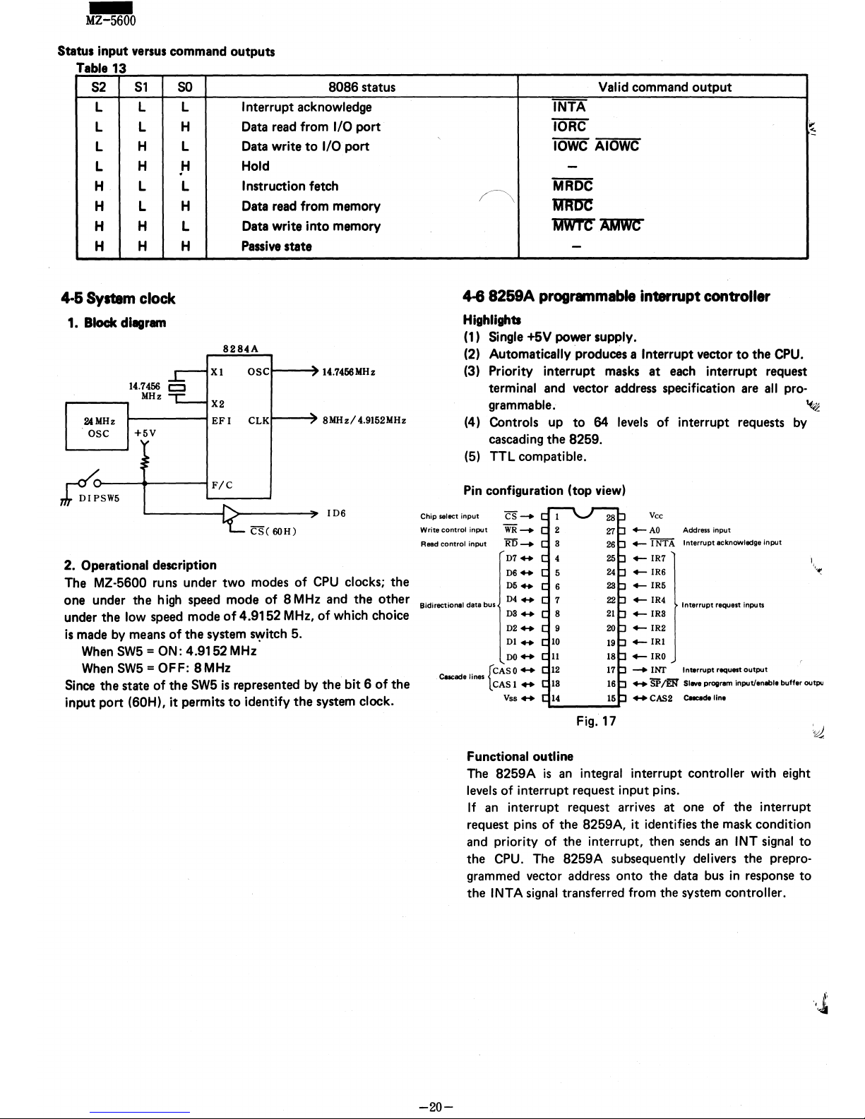
Status input versus command
outputs
Table
13
S2
S1
L
L
L L
L
H
L
H
H L
H L
H H
H H
4·5 System clock
1.
Block diagram
SO
L
H
L
H
L
H
L
H
14.7456
c:J
MHz
8086
status
Interrupt acknowledge
Data read from
I/O
port
Data write
to
I/O
port
Hold
Instruction
fetch
Data read from memory
Data write into memory
Passive state
8284A
X 1
OSCI--~
14.7456MHz
X2
24MHz
1------1
EF
1
CLKt---~
8MHz/4.9152MHz
osc
+5V
~~--~~----~F/C
J,
DIP
SW5
1...-
__
---'
106
CS(
SOH)
2. Operational description
The
MZ-5600 runs under
two
modes
of
CPU
clocks;
the
one under
the
high speed mode of 8 M
Hz
and the
other
under
the
low speed mode
of
4.9152
MHz,
of
which choice
is
made by means
of
the
system s\!"itch 5.
When
SW5
= ON: 4.9152
MHz
When
SW5
= OFF: 8MHz
Since the state of
the
SW5
is
represented by
the
bit 6
of
the
input
port
(60H), it permits
to
identify
the
system clock.
Valid command
output
INTA
10RC
10WC
AIOWC
-
i-----'-
MRDC
~
'MW'rn"
AMWc
-
4-8 8259A programmable interrupt controller
Highlights
(1) Single +5V power supply.
(2) Automatically produces a
Interrupt vector
to
the CPU.
(3) Priority interrupt masks
at
each interrupt request
terminal and vector address specification are
all
pro-
grammable.
~
(4) Controls up
to
64 levels of interrupt requests by
cascading
the
8259.
(5)
TTL compatible.
Pin configuration
(top view)
Chip
select
input
CS_
Vcc
Write
control
input
WR
-+
Read
control
input
Ri5
-+
07_
06_
05_
Bidirectional data bus
04_
03_
02_
DJ_
00-
~
CASO++
CUcade lines
CAS!
...
Vss_
Functional outline
Fig. 17
4--
AO
Address input
+-
I
NTA
Interrupt acknowledge input
4-
IR7
4-
IR6
4-
IR5
4-
IR4
4-IRa
4-IR2
_IRI
_IRO
Interrupt
request
inputs
--+
INf
Interrupt
request
output
......
SP!EFl'
Sieve program input/enable
buffer
outpu
++
CAS2
Coocadolino
The
8259A
is
an integral interrupt controller with eight
levels
of
interrupt request input pins.
-20-
If
an interrupt request arrives at one of the interrupt
request pins of the 8259A, it identifies the mask condition
and priority of the interrupt, then sends an
INT signal
to
the CPU. The 8259A subsequently delivers the preprogrammed vector address onto the data bus
in
response
to
the INTA signal transferred from the system controller.
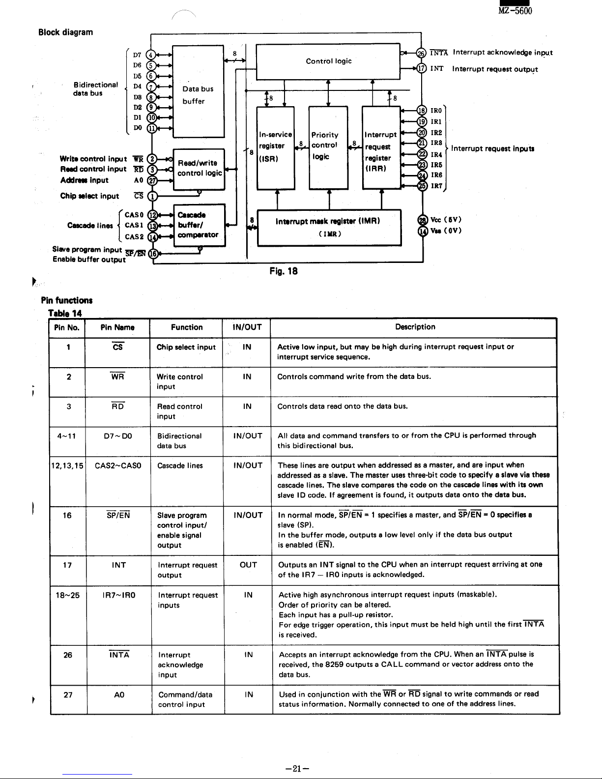
Block diagram
07
06
D5
Bidirectional
04
Data bus
dlta
bus
D8
buffer
D2
01
DO
Write
control
input
RIId
control
Input
Addretllnput
AO
Chip
.Iact
input
CS
r'"
Cascade
lines
CAS
1
CAS
2
Slavl program
input
m;;m
Enable
buffer
output
~.
Pin
functions
Tabl.14
Pin No. Pin Name
Function
1
CS
Chip
select
input
2
WR
Write
control
input
3
RD
Read
control
input
4-11
07-00
Bidirectional
data bus
12.13.15
CAS2-CASO
Cascade
lines
16 SP/EN
Slave
program
control
input/
enable signal
output
17
INT
I
nterrupt
request
output
18-25
IR7-IRO
Interrupt
request
inputs
26
iNTA
Interrupt
acknowledge
input
27
AO
Command/data
control
input
8
Control
logic
-
MZ-5600
TN'i'A
I
nterrupt
acknowledge
inl?U.t
INT
Interrupt
request
outp'!t
In-service
Priority
IRO
IRl
IR2
IRa
IR4
IR5
IR6
register
8
control
8
request
Interrupt
request Inputs
8
(lSR)
logic
register
IN/OUT
IN
IN
IN
IN/OUT
IN/OUT
IN/OUT
OUT
IN
IN
IN
(lRR)
L-_~..I"-"C!J
IRT
InterNpt m ..
k register
(lMR)
(ID)
Fig. 18
Vcc
(aY)
v
..
(OV)
Description
Active
low
input.
but
may be high
during
interrupt
request
input
or
interrupt
service sequence.
Controls command
write
from
the
data bus.
Controls data read
onto
the data bus.
All
data and command transfers
to
or
from
the
CPU
is
performed through
this bidirectional bus.
These
lines are
output
when addressed
as
a master. and are
input
when
addressed
as
a slave. The master
uses
three-bit code
to
specify a slave via these
cascade
lines. The slave compares the code on
the
cascade lines
with
its
own
slave
ID
code.
If
agreement
is
found.
it
outputs
data
onto
the
data bus.
In normal mode. SP/EN = 1 specifies a master. and SP/EN = 0 specifies a
slave (SPI.
In
the
buffer
mode.
outputs a low
level
only
if
the data bus
output
is
enabled (EN).
Outputs
an
INT
signal
to
the
CPU
when
an
interrupt
request arriving
at
one
of
the
IR7
- IRO inputs
is
acknowledged.
Active high asynchronous
interrupt
request inputs (maskablel.
Order
of
priority
can
be
altered.
Each
input
has a pull-up
resistor.
For
edge
trigger operation. this
input
must
be
held high
until
the
first
INTA
is
received.
Accepts
an
interrupt
acknowledge
from
the CPU. When
an
INTA
pulse
is
received.
the
8259
outputs a CALL
command
or
vector address
onto
the
data bus.
Used in
conjunction
with
the
WA
or
AD
signal
to
write
commands
or
read
status
information.
Normally
connected
to
one
of
the
address lines.
-21-
-
MZ-5600
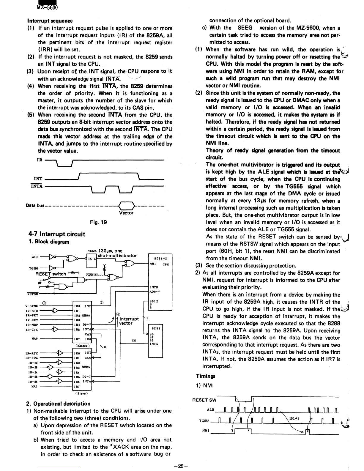
Interrupt sequence
(1)
If
an
interrupt request pulse
is
applied
to
one or more
of
the interrupt request inputs (lA) of the 8259A,
all
the pertinent bits of the interrupt request register
(I A
A)
will
be
set.
(2)
If
the interrupt request
is
not masked, the 8259 sends
an
INT signal
to
the
CPU.
(3) Upon receipt
ot
the
INT signal, the
CPU
respons
to
it
with an acknowledge signal
INTA.
(4)
When
receiving the first
'JNTA,
the
8259 determines
the order of priority. When it
is
functioning
as
a
master, it outputs the number of the slave for which
the
interrupt
was
acknowledged,
to
its
CAS
pin.
(5)
When
receiving the second
JNTA
from the
CPU,
the
8269 outputs an 8-bit
inte~rupt
vector address onto the
data bus synchronized with the second
INTA.
The
CPU
reads this vector address
at
the trailing edge
of
the
INTA, and jumps
to
the interrupt routine specified by
the vector value.
IR~
INT
____
.... '
\'----
'iNTA
------"'""'\
Data
bus-------
-----------0--------
Vector
Fig.
19
4-7 Interrupt circuit
1. Block diagram
TG666
V-SYNC
IR-SIO
IR-PRT
IR-KEY
IR-NDP
IR-CTC
!lAO
lR-RTC
IR-FOC
IR-22
IR..,28
IR-24
IR-26
IR-26
!lA
I
8086-2
NUl
CPU
.--------IINTR
,------___iADO-7
<D
CID
-""---___i
I
RO I NT!-""::""--'
--~>-___i
IRI
-----I
IR2
8269A
ill
-----lIRa
j
11
nterrupt
-----IIR4
00-71-----+
vector
---<1"">---1
IR6
INT~---+-'
CA5
SOl2
5
5
8288
50
51
CID
52
t-----""--___i
I
NT
A
--~.>_-1
IR2
-·<D---1
I
Ra
8269A
IR4
:>-----1
I
R6
00-71----
......
--~.>_-1
IR6
INT'A!E------'
------iIR7
(Slave)
2. Operational description
1)
Non-maskable interrupt
to
the
CPU
will
arise under one
of the following two (three) conditions.
a)
Upon depression of the A ESET switch located on the
front side
of
the unit.
b)
When
trjed
to
access a memory and I/O area not
existing, but limited
to
the *XACK area on the map,
in
order
to
chock an existence
of
a software bug
or
-22-
connection
of
the
optional board.
c)
With
the
SEEG version
of
the MZ-5600, when a
certain task tried
to
access
the
memory area not per-
mitted
to
access.
(1) When
the
software has run wild, the operation
is::
normally halted by turning power off
or
resetting the
~
CPU.
With this model
the
program
is
reset by
the
soft~
ware using
NMI
in
order
to
retain
the
AAM,
except for
such a wild program run that may destroy
the
NMI
vector
or
NMI
routine.
(2)
Since this unit
is
the
system
of
nonnally non-ready, the
ready signal
is
issued
to
the
CPU
or
DMAC
only when a
valid memory or
I/O
is
.accessed.
When
an
invalid
memory
or
I/O
is
accessed,
it
makes the system
as
if
halted. Therefore,
if
the ready signal has not returned
within a certain period,
the
ready signal
is
issued from
the
timeout circuit which
is
sent
to
the
CPU
on
the
NMlline.
Theory
of
ready signal generation from
the
timeout
circuit.
The one-shot multivibrator
is
triggered and its
output
,
is
kept high by
the
ALE signal which
is
issued
at
the~
start
of
the
bus cycle, when
the
CPU
is
continuing
effective access,
or
by
the
TG555 signal which
appears
at
the
last stage
of
the
DMA
cycle
or
issued
normally at every
13
f.lS
for memory refresh, when a
long internal processing such
as
multiplication
is
taken
place. But, the one-shot
l;1lultivibrator output
is
in
low
level
when an invalid memory or I/O
is
accessed
as
it
does not contain
the
ALE
or
TG555 signal.
As
the state
of
the
AESET switch can
be
sensed
by~,j
means of the
ASTSW
signal which appears on the input
port
(60H, bit 1),
the
reset
NMI
can
be
discriminated
from the timeout
NMI.
(3)
See
the section discussing protection.
2)
As
all
interrupts are controlled
by
the 8259A except for
NMI,
request for interrupt
is
informed
to
the
CPU
after
evaluating their priority .
When
there
is
an interrupt from a device by making the
I A input
of
the
8259A high, it causes the
INTA
of
the·
CPU
to
go
high,
if
the I A input
is
not masked.
If
the~
CPU
is
ready for acception of interrupt, it makes the
interrupt acknowledge cycle executed
so
that
the 8288
returns the
INTA signal
to
the 8259A. Upon receiving
INTA, the 8259A sends on the data bus the vector
corresponding to
that
interrupt request.
As
there are two
I
NT
As,
the interrupt request must
be
held until the first
INTA.
If
not, the 8259A assumes the action
as
if
IA7
is
interrupted.
Timings
1)
NMI
RESETSW
TG556
-.J'---'4-...J
NMI
___
..J
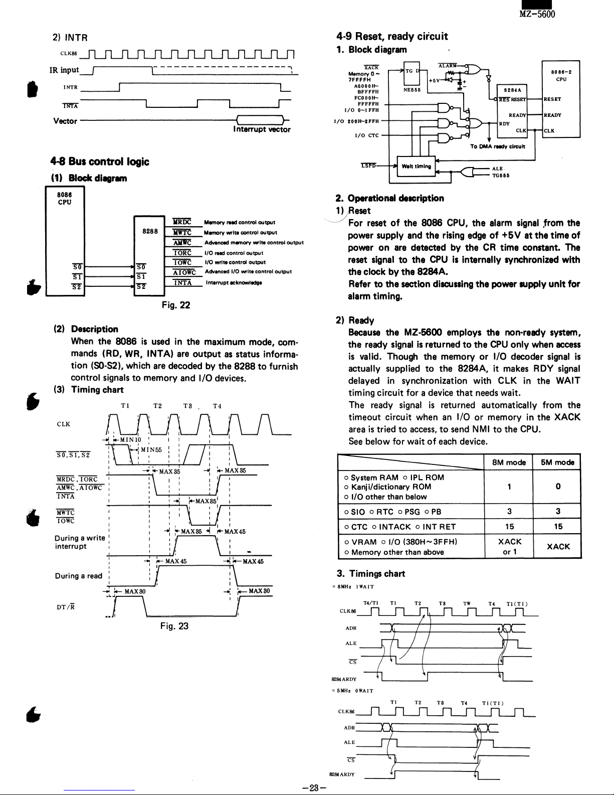
I
2)
INTR
CLK86
IR
input---.J
INTR
L
TJifI'A
L-..
__
----I'
Vector ( r
I ntarrupt vector
4-8
BUI
control logic
m Block dlllllram
808e
CPU
8288
so so
n
ST
n
n
iiROC
1iW'i'C
AIIWC
IORC
loic
AlotC
INTA
Fig. 22
Mlmary
IHd
control
output
Momory
wrIt.
_trol
output
Advtlncod mllllary wrIte control
output
1/0
IHd
control
output
I/O write control
output
Advoncod 1/0 write control
output
Interrupt
..
kn_odatt
(2) Description
When
the 8086
is
used in the maximum mode, com-
mands (RD,
WR,
INTA) are
output
as status informa-
tion
(SO-S2),
which are decoded by
the
8288
to
furnish
control signals
to
memory and I/O devices.
(3) Timing chart
eLK
During a
write
interrupt
Tl
T2
Ta
T4
I '
,
,
, '
.
____
r---t'_=!j.:J.'...,io-
MAX
851 ,.....;.'----
~
l'lJJ'
,I
: I :
I I I I
-.:
:",MAX85
-oi
"'-MAX45
If
\ :
+-----"-.~-MA~X~
~~~'~-MAX--~-
. -:-
___
:,....J/',
:;
\L--""~~
During a
read
'T"'
,....
~'n:-
MAX80
--!
fMAX80
DT/R
••
I •
Fig.
23
4-9 Reset, ready circuit
1. Block diagram
~
Memory
0-
7FFFFH
AOOOOft-
BFFFFH
FCOOOH-
FFFFFH
-+-
________
_
I/O
O-IFFH
I/O
IOOft-UPH
-4-~--;-",
I/O
CTC
-I---+-+--r-'\
-
MZ-5600
8088-2
CPU
8284A
RESET
READY READY
RDY
CLK
CLK
2. Operational description
Yoeset
, For reset
of
the
8086 CPU,
the
alarm
Signal
.from the
power
supply and
the
rising edge
of
+5V
atthe
time
of
power
on
are detectad by
the
CR
time constant. The
reset
signal
to
the
CPU
is
Internally synchronized with
the
clock by
the
8284A.
Refer
to
the
section dlscuulng
the
power supply unit for
alarm timing.
2) Ready
Because the
MZ-5600 employs the non-ready system,
the
ready signal
is
returned
to
the
CPU
only when access
is
valid. Though
the
memory
or
I/O decoder signal
is
actually supplied
to
the 8284A, it makes
RDY
signal
delayed
in
synchronization with
CLK
in
the
WAIT
timing circuit for a device
that
needs wait.
The ready
signal
is
returned automatically from the
timeout circuit when
an
I/O
or
memory
in
the
XACK
area
is
tried
to
access,
to
send
NMI
to
the
CPU.
See below for wait
of
each device.
8M mode
5M mode
o
System RAM 0 IPL ROM
o Kanji/dictionary ROM
1
0
o 1/0 other than below
oSlO
0 RTC 0
PSG 0 PB
3 3
o CTC
olNTACK 0 INT
RET
15 15
o
VRAM
0110
(380H-3FFH)
XACK
XACK
o Memory other than
above
or
1
3. Timings chart
o 8MHz 1
WAIT
HITI
Tt
T2
T8
TW
o 611Hz
aWAIT
TI
T2
Ta
T4
TI(TI)
-23-
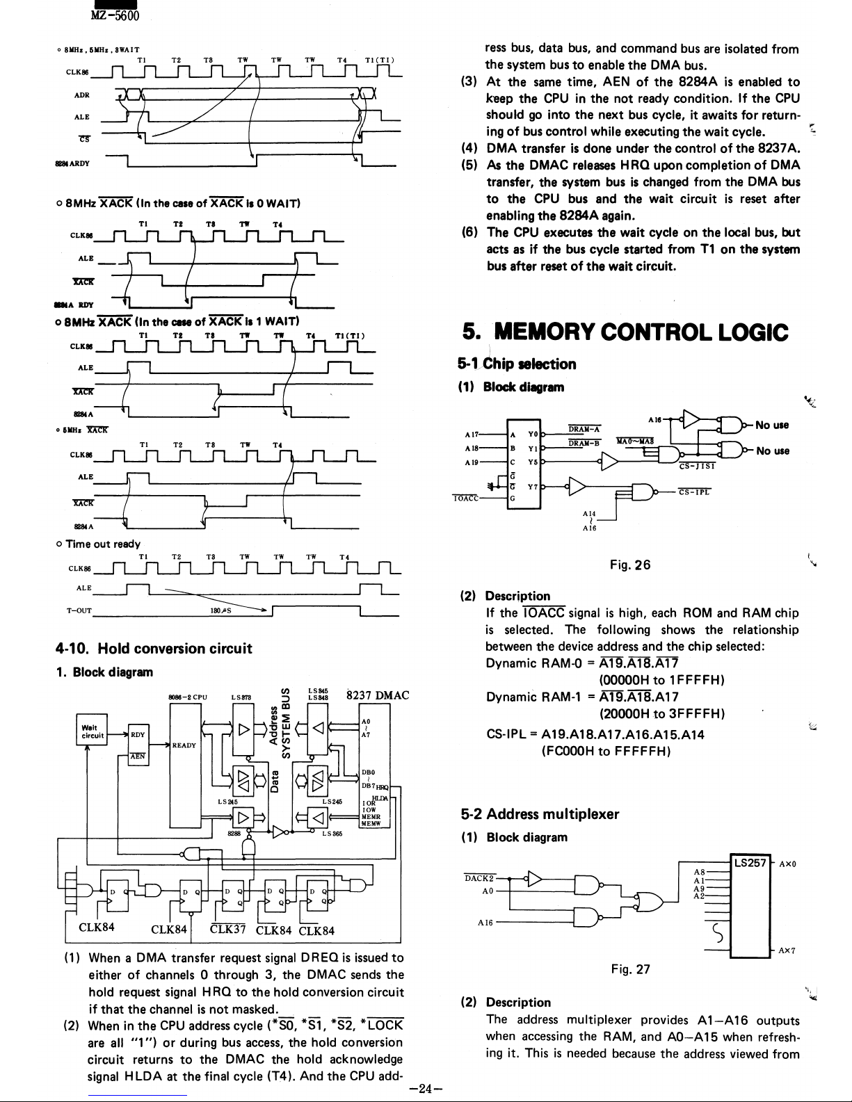
o
811H.,
611Hz.
aWAIT
Tl
CLK8B
ADR
ALE
Tt
TW TW
o 8MHz XACK (In the cell
ofXACKl1
0 WAIT)
Tl
Tt
TI
T1I
TC
=~
_"lIlY
_
o 8MHz
XACK
(In the
C8II
of
XACK
I1 1 WAIT'
Tl
TI TI
T1I T1I
TC
TI(
T
J)
~~
• IIIBI
'ltIJr
T1
T2
T8
TW
Tt
~~
o Time out ready
Tl
Tt
Ta
TW
TW TW
T4
CLK8B
ALE -I"i_==-=--==-""""'
___________
...JIL
T-OUT
_______
---s==:--::lllO:.;.I'..:.S
__
.....J
1
.......-----
.....
L--
4-10. Hold conversion circuit
1. Block diagram
8088-2
CPU LS878
LSIM/i
LS848
8237
DMAC
(1)
When a DMA
transfer request
signal
DREQ
is
issued
to
either
of
channels 0 through 3, the DMAC
sends
the
hold request signal H
RQ
to
the hold conversion circuit
if
that the channel
is
not
masked.
(2)
When
in the
CPU
address
cycle (*SO, *S1, *S2,
*LOCK
are
all
"1")
or
during
bus
access,
the hold conversion
circuit returns
to
the DMAC the hold acknowledge
signal H
LDA
at the final cycle (T4). And the
CPU
add-
-24-
ress
bus, data
bus,
and command
bus
are
isolated from
the system
bus
to
enable the
DMA
bus.
(3)
At
the
same
time, AEN
of
the 8284A
is
enabled
to
k'eep
the
CPU
in the
not
ready condition.
If
the
CPU
should go
into
the
next
bus
cycle,
it
awaits
for
return-
ing
of
bus
control while executing the
wait
cycle.
(4)
DMA
transfer
is
dona under the control
of
the 8237A.
(6)
As
the DMAC
releases
HRQ
upon completion
of
DMA
transfer, the system
bus
is
changed from the
DMA
bus
to
the
CPU
bus and the wait circuit
is
reset after
enabling the
8284A
again.
(6) The
CPU
executes the
wait
cycle on the local bus, but
acts
as
if
the
bus
cycle started from
T1
on the system
bus
after reset
of
the
wait circuit.
5.
MEMORY
CONTROL
LOGIC
5-
,lhiP
selection
(1) Block diagram
(2) DescriPtion
Fig.
26
If
the IOACC signal
is
high,
each
ROM
and
RAM chip
is
selected. The following
shows
the relationship
between the device
address
and
the chip selected:
Dynamic RAM-D
=
AfS.A
1B.A 17
(ODODOH
to 1 FFFFH)
Dynamic RAM-1 =
AfS.A18.A17
(20ODOH
to
3FFFFH)
CS·IPL = A19.A18.A17.A16.A15.A14
(FCOODH
to
FFFFFH)
5-2 Address multiplexer
(1) Block diagram
'iiACK2
AO
-t----L..-I
AI6------I
Fig.
27
(2) Description
s
LS257
AXO
AX1
L.-_-'
The
address
multiplexer provides A
1-A
16 outputs
when
accessing
the RAM, and
AO-A
15 when refresh·
ing
it.
This
is
needed
because
the
address
viewed
from
I
'10
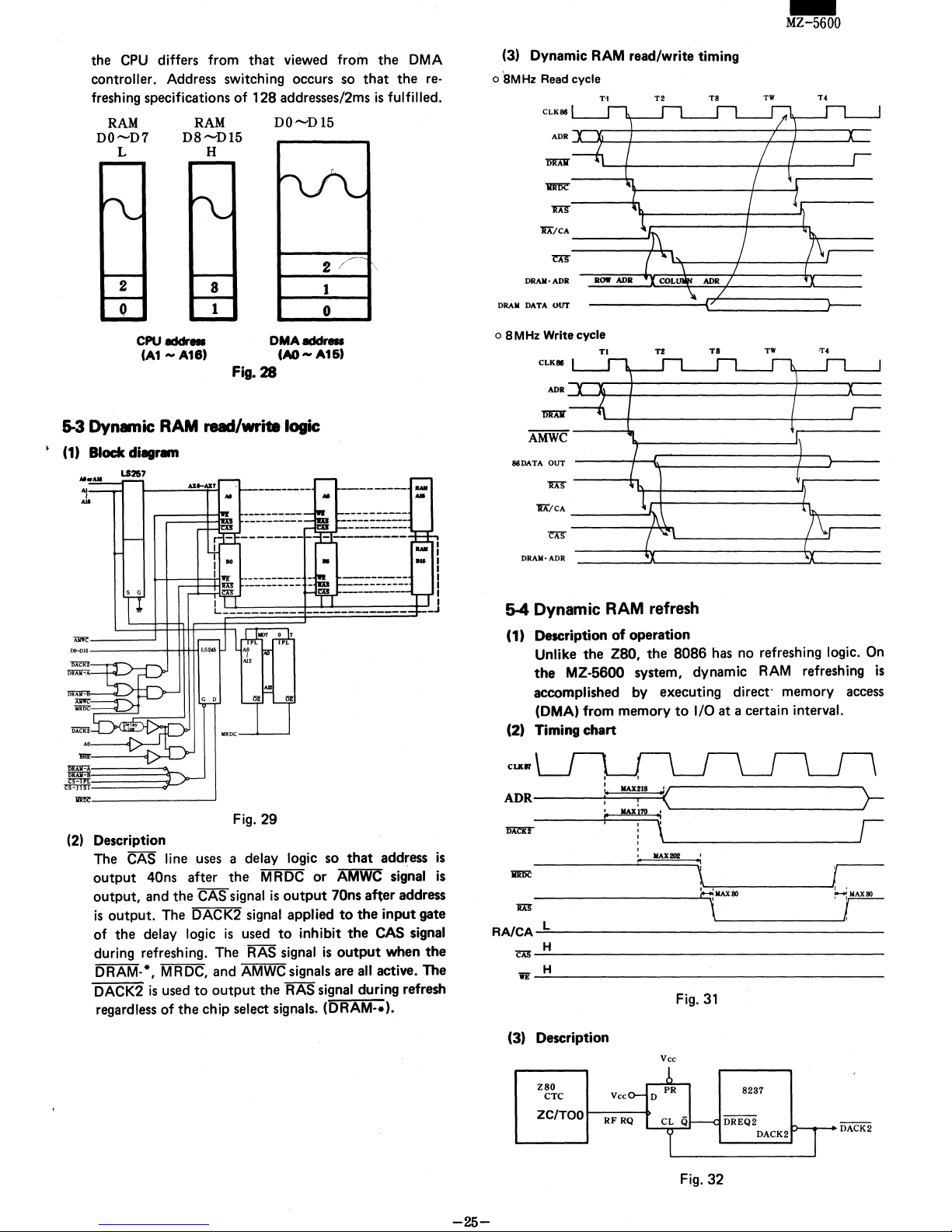
the
CPU
differs from
that
viewed from
the
DMA
controller. Address switching occurs so
that
the
re·
freshing specifications
of
128
addresses/2ms
is
fulfilled.
RAM
DO-D7
L
2
o
RAM
D8-D15
H
8
1
CPUIddr.
(A1
- A18)
DO-D15
2
1
o
OMAaddr.
(AD-
A16)
Fig. 28
5-3
Dynamic
RAM
read/write logic
• (1) Block
dieg,."
......
AI
L.S267
...
..
I
AI
All
=------'
Fig.
29
(2) Description
The
CAS line uses a delay logic so
that
address
is
output
40ns after
the
MRDC
or
AMWC
signal
is
output,
and
the
CAS
signal
is
output
70ns
atter
address
is
output.
The DACK2 signal applied
to
the
input
gate
of
the
delay logic
is
used
to
inhibit
the
CAS signal
during refreshing. The
RAS signal
is
output
when
the
BR'Ai\.1.
*,
M R
DC,
and
AMWC
signals are all active. The
DACK2
is
used
to
output
the
RAS signal during refresh
regardless
of
the
chip select signals. (DRAM-.).
-25-
-
MZ-5600
(3) Dynamic RAM read/write timing
o 'SMHz
Read
cycle
T2
TB
TW
CLK86
ADR~~
__ ~ ______________
~L-~
____
~~
RA/CA
-------.....11
DRAM·ADR
DRAM
DATA
OUT
o
8MHz
Write cycle
CLKIIII
~R-A~~~
__________________
-+
______ ~ __
86DATA
OUT
1!A/CA
____
.....I)
DRAM·ADR
5-4 Dynamic RAM refresh
(1) Description
of
operation
Unlike
the
Z80,
the
8086
has no refreshing logic. On
the
MZ-5600 system, dynamic
RAM
refreshing
is
accomplished by executing direct· memory access
(DMA) from memory
to
I/O
at
a certain interval.
(2) Timing
chart
CutrT
ADR
---~~~.\
~
_
______
~I·==~==l=ro~'~--------------------~
r;;ren-
\ r
IIAX202
iiiliC
RE
L
\~---'-
-------------------~~~~
~~
RA/CA
~
H
WE
H
(3) Description
Z80
CTC
Vcc
ZC/TOO
r--RF-R-Q~
Vcc
PR
D
Fig.
31
CL
Q
Fig.
32
8237
DACK2
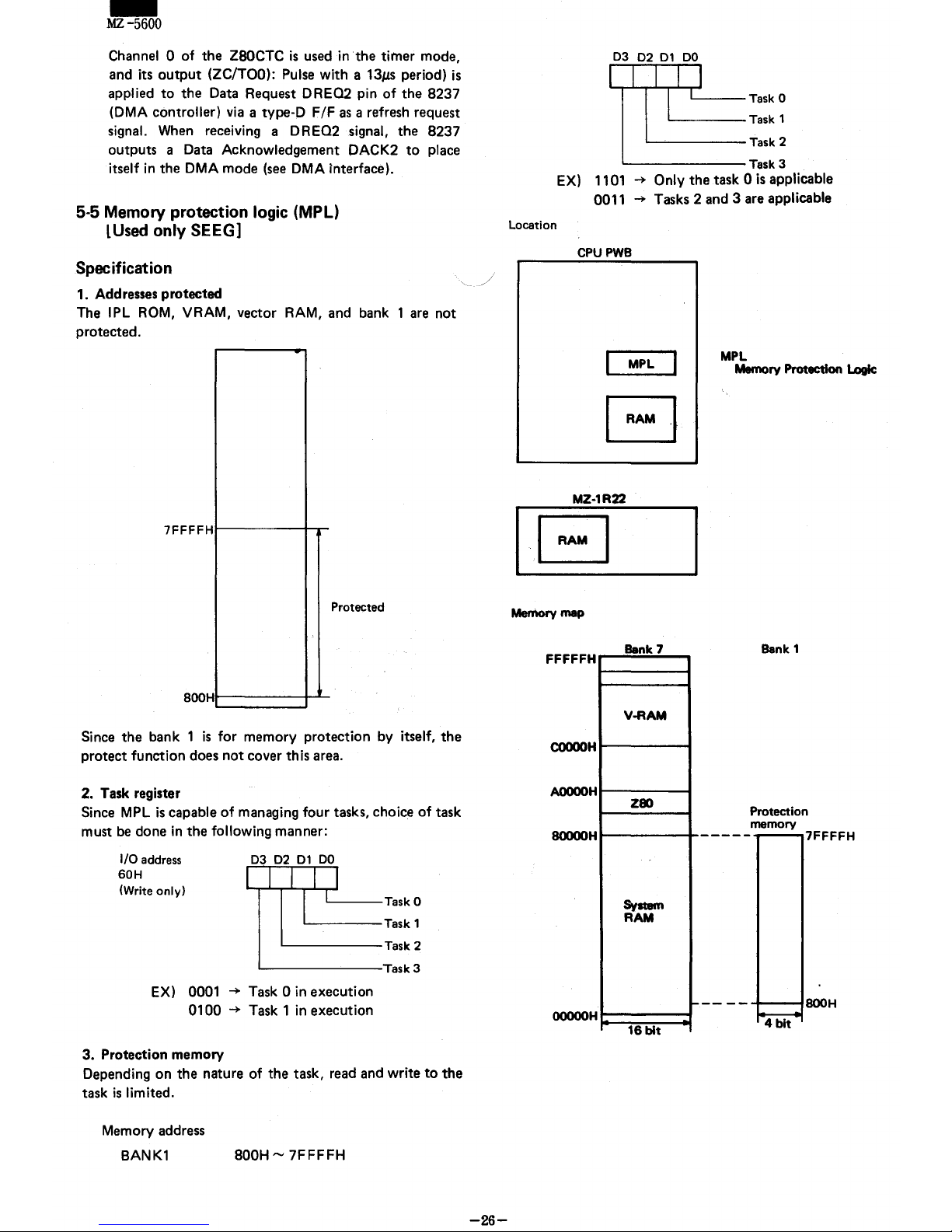
-
MZ-5600
Channel 0 of
the
lBOCTC
is
used
in
the
timer mode,
and its
output
(lC/TOO): Pulse with a
13J,tS
period)
is
applied
to
the
Data Request DREQ2 pin
of
the
8237
(DMA controller)
via
a type-D
F/F
as
a refresh request
signal. When receiving a DREQ2 signal,
the
8237
outputs
a Data Acknowledgement DACK2
to
place
itself
in
the
DMA
mode (see
DMA
interface)_
5-5 Memory protection logic (MPL)
LUsed
only SEEG]
Specification
1. Addresses protected
The
IPL
ROM,
VRAM, vector RAM, and bank 1 are not
protected.
7FFFFH~------~~
Protected
800HIr---------f-L.
Since
the
bank 1
is
for memory protection by itself,
the
protect
function does
not
cover this area.
2. Task register
Since
MPL
is
capable
of
managing four tasks, choice
of
task
must be done
in
the
following manner:
I/O address
60H
(Write only)
03
02
01
DO
I I I I I
I
IL.-----Task
0
'-------Task
1
L------Task
2
'--------------Task
3
EX)
0001 ~ Task 0
in
execution
01
00 ~ Task 1
in
execution
3.
Protection memory
Depending
on
the
nature of
the
task, read and write
to
the
task
is
limited.
Memory address
BANK1
800H -
7FFFFH
-26-
03
02
01
DO
I I I I I
l
'----Task 0
'------Task
1
'-------Task
2
'--------------
Task 3
EX)
11
01 ~ Only
the
task 0
is
applicable
0011
~
Tasks 2 and 3 are applicable
Location
CPUPWB
MPL
MZ-1R22
II~
Memory
map
Bank 7
FFFFFH
V-RAM
COOOOH
AOOOOH
zao
SOOOOH
System
RAM
OOOOOH
16
bit
r
MPL
Memory
ProtectIon
l...ogIc
Bank 1
Protection
memory
..,.--..,7
F F F F H
-t---tSOOH
~

Block Diagram
of
Memory Protection
ADO
l
AD19
8088
CPU
NUl
COMMAND
8237
DMAC
r-
______________
~ADD
CAS
RAS
SYSTEM
RAM
(S12KB)
CRTL
I-----......ct
>-----'
-
MZ-5600
DD
~--r-r-----------,n
~~~~n
r7----RESET
SW
L..-
________
-{
-...Jp---Timer
MPL
operation
When
four tasks are operated simultaneously in
the
time
shared mode, every task
is
allocated
to
the
system
RAM
area (512
KB,
max.).
If
a task should
try
to
access
the
system
RAM
beyond
the
limit,
not
only
the
RAM
is pro-
tected, but also
the
condition
is
sensed and informed
to
the
CPU
with
NMI.
Since the currently operating task is
set
in
the
task
register
(output on
ilo address
60H),
the
task information should
be
set by
the
OS
each time
the
task changes.
One word (4 bits)
of
the
protection memory corresponds
to
one kilobytes
of
the system
RAM,
which
is
used
to
indicate
the system
RAM
area
the
task can
access.
To
enable
the
use
of
the 1 KB
area
of
54400H through
547FFH
for
the
tasks
1 and 2 and
to
disable tasks 0 and
3,
for
instance.
"1001"
has
to
be set
in
the
protect memory.
MPL
does
not
func-
tion
at
power on and when
"0"
is
set in
the
task register.
Shown next
is
the
procedure
to
set
up
the
protection
memory area.
Theory
of
memory protection
For instance,
the
protection
RAM
area 10000H
of
the
bank
1 contains
"1010"
to
enable
the 1 KB
area
of
the
system
RAM
1000H - 103FFH for access by tasks 0
and
2.
If
the
system
RAM
area
of
1000H -
103FFH
is tried
to
-~-
RAM
C1K
x4)
I/O
Task 3
~ection
Logic
read
or
write during
the
execution
of
the task 1 with
"0010"
in
the
task register,
the
data
"1010"
is
sent from
the
protection
RAM.
Then,
the
protection data
"1010"
is
Ored
with
"0010"
of
the
task register by
the
protection
logic. Since
the
result would not be
"0000"
but
"0010",
it
prohibits
CAS signal from
the
system
RAM.
For the
dynamic RAM.
the
same cycle
as
the
RAS
only fresh
is
executed. which in consequence disables
to
read or write
to
the
RAM.
At
the
same time,
the
NMI
is
issued
to
the
CPU
with
the
CAS inhibit signal.
The reason why CAS
is
prohibited for protection
of
the
memory
is
that
it
is
not
practically possible
to
use a
high
speed
protection
RAM
and
the
protection logic which are
required
to
disable
the
read
or
write command using the
address information.
WAVEFORMS
·1:
The protection data are sampled
at
a high
to
low transi·
tion
of
the
command and
the
contents of the task
register
is
operated and CASINH
is
forced active
if
required. CAS would
not
go active
as
long
as
CASINH
is active.
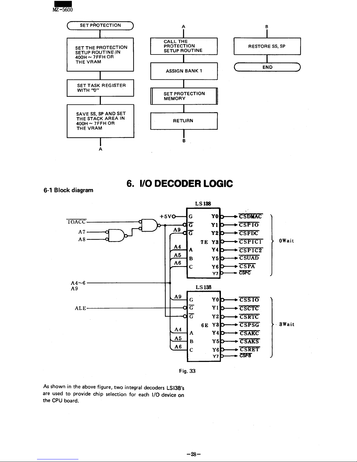
-
MZ-5600
SET
PRoTECTION
A
I ,
I
CALL
THE
SET
THE
PROT~CTION
SETUP
ROUTINE\IN
PROTECTION
SETUP
ROUTINE
400H ~ 7FFH
OR
THE
VRAM
I
I
ASSIGN
BANK
1
SET
TASK
REGISTER I
WITH
"0"
SET PROTECTION
I
MEMORY
SAVE
SS,
SP
AND
SET
I
THE
STACK
AREA
IN
400H ~ 7FFH
OR
RETURN
THE
VRAM
I
I
B
A
6.
I/O DeCODER LOGIC
6-1
Block diagram
LSI88
+5Vo--
G
YO
~
IOACC
J'
G
YI
~
A~
G
A7
Y2
~
~
A8
7E
YS
~
A
Y4
~
B
Y5
I"'"
AS
-
C
YS
Y7
A4-S
A9
LSI38
A9
G
YO
ALE
l'
G
YI
....
l'
G
Y2
....
SE
YS
....
A4
A
Y4'"
A5
B
Y5
....
AS
C
YSlo..
-
Y7
Fig.
33
As
shown in the above figure,
two
integral decoders LS138's
are used
to
provide
chip
selection
for
each
I/O
device
on
the
CPU
board.
-28-
B
I
RESTORE
SS,
SP
1
END
)
~
CSDMA!
c
CSPIO
CSFOC
CSPIC
1
OWait
CSPIC
2
CSUAD
CSPA
BJ5C
CSSIO
CSCTC
CSRTC
CSPSG
.
SWait
CSAKC
CSAKS
eSRET
~
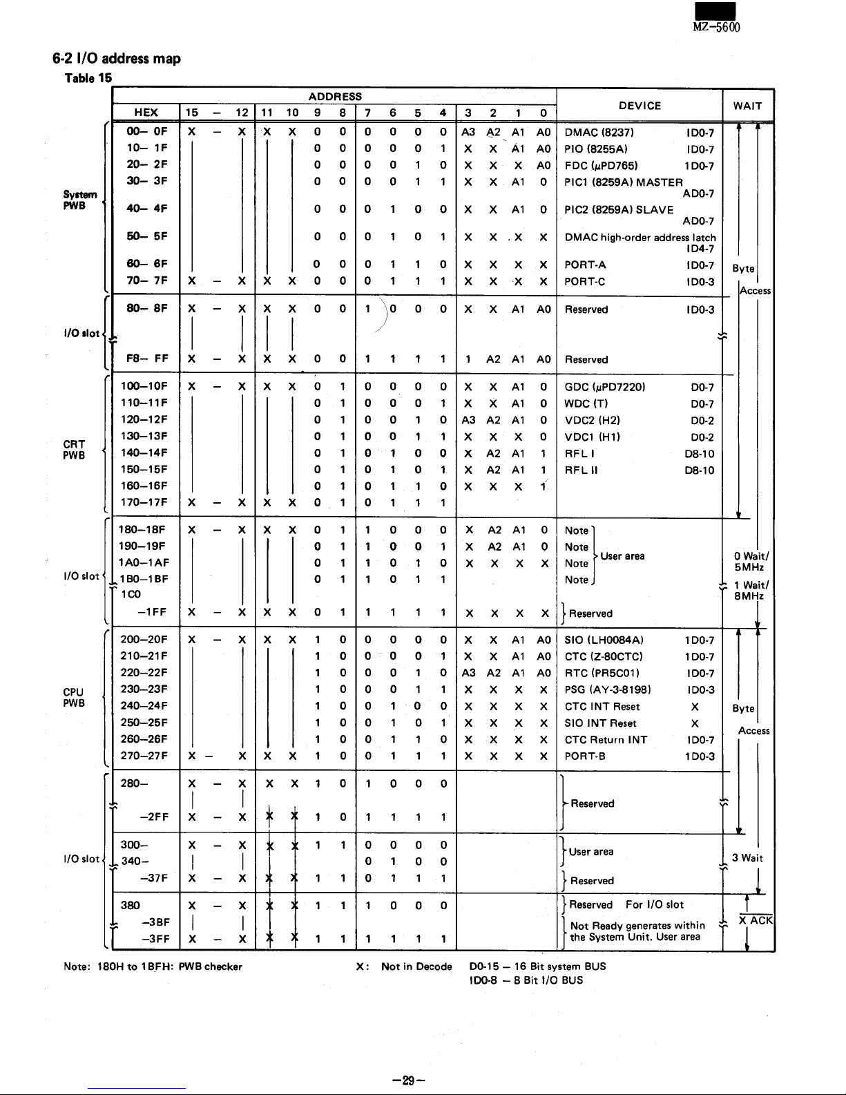
6·2 I/O address map
Table
15
System
PWS
I/O
Ilot
CRT
PWB
I/O slot
CPU
PWB
I/O slot
{
HEX
00-
OF
10-
1F
20-
2F
30-
3F
40-
4F
60-
5F
60-
6F
70-
7F
SO-
SF
FS-
FF
1oo-10F
110-11F
120-12F
130-13F
140-14F
150-15F
160-16F
170-17F
1 SO-1
SF
190-19F
1AO-1AF
1
BO-1BF
1CO
-1FF
200-20F
210-21F
220-22F
230-23F
240-24F
250-25F
260-26F
270-27F
2S0-
-2FF
300-
340-
-37F
3S0
-3BF
-3FF
15
-
12
X
-
X
X
-
X
X
-
X
I
I
X
-
X
X
-
X
X
-
X
X
-
X
X -
X
X
-
X
X
-
X
X
-
X
I
I
X
-
X
X
-
X
I I
X
-
X
X
-
X
I I
X
-
X
Note:
1S0H
to
1 BFH:
PWB
checker
11
10
X
X
X X
X X
I
I
X X
X X
X X
X
X
X
X
X X
X
X
X
X
*
!
t
~
-
MZ-5600
ADDRESS
9
S
0
0
0 0
0 0
0 0
0 0
0
0
0
0
0 0
0 0
0 0
0
1
0 1
0 1
0
1
0 1
0 1
0
1
0 1
0 1
0 1
0 1
0 1
0 1
1
0
1 0
1
0
1 0
1
0
1 0
1 0
1 0
1
0
1 0
1 1
1 1
1
1
1 1
7 6
5
4
3 2 1
0
DEVICE
0
0
0 0
A3
~2
A1
AO
OMAC (S237)
100-7
-
0 0
0
1
X X
A1
AO
PlO (S255A)
100-7
0 0
1
0
X X
X
AO
FOC (j.lP0765)
100-7
0
0
1 1
X X
A1
0
PIC1
(S259A) MASTER
AOO-7
0 1
0 0 X
X
A1
0
PIC2 (S259A)
SLAVE
AOO-7
0 1 0 1
X X
.X
X
OMAC high-order
address
latch
104-7
0
1 1
0 X X
X
X PORT-A
100-7
0
1
1
1
X X
'X
X PORT-C
100-3
1
)0
0
0
X X
A1
AO
Reserved
100-3
1 1 1 1 1
A2
A1
AO
Reserved
0 0 0
0
X
X
A1
0
GOC (j.lP07220)
00-7
0 0
0
1 X
X
A1
0
WOC
(T)
00-7
0
0
1
0
A3 A2
A1
0
VOC2 (H2)
00-2
0
0
1 1
X X X
0 VOC1 (H1)
00-2
0
1 0
0
X
A2
A1
1
RFLI
OS-10
0 1
0 1
X
A2
A1
1
RFL
11
OS-10
0 1 1 0
X X X
{
0 1 1 1
1
0 0 0
X
A2
A1
0
NO"}
1
0
0
1 X A2
A1
0
Note
1
0 1 0
N User
area
X
X
X
X ote
1
0 1 1
Note
1 1 1 1
X X
X X
} Reserved
0 0 0 0
X X
A1
AO
SIO
(LH0084A)
100-7
0
0 0
1 X
X
A1
AO
CTC (Z-SOCTC)
100-7
0
0
1 0
A3 A2
A1
AO
RTC (PR5C01)
100-7
0 0
1 1 X X
X X
PSG
(AY-3-S19S)
100-3
0
1 0
0 X X X X CTC I
NT
Reset
X
0 1 0 1
X X X X
SIO
INT
Reset
X
0 1 1 0
X X X X CTC Return
INT
100-7
0
1 1 1 X
X X X
PORT-B
100-3
1
0 0 0
}R~~
1 1 1
1
0 0 0 0
}user
area
0 1
0
0
0
1 1 1
} Reserved
1
0 0
0
} Reserved For
I/O
slot
1 1
1
1
}
Not
Ready generates
within
the System
Unit.
User
area
X:
Not
in Decode
00-15
- 16
Bit
system BUS
100-S
- S
Bit
I/O
BUS
-29-
WAIT
Byte
Access
o Wait/
5MHz
~
1 Wait/
SMHz
Byte
Access
3 Wait
~
!
-L
:
X1ACK
 Loading...