

Page 1
MZ-3500
SERVICE MANUAL
CODE:
OOZMZ
3500SM/E
r C
PERSONAL COMPUTER
MODEL
MZ-350C
CONTENTS
1.
Specifications
1
2.
Software (Memory)
Configuration
7
3. CPU and
memory
12
4. CRT
display
25
5. MFD
Interface
52
6.
R232C Interface
72
7.
Printer Interface
7g
8.
Other Interface
81
9.
Power
Circuit
discription
37
10.
Keyboard Controller Circuit
discription
QQ
11.
Seif
check functions
94
12. IPL
flow
chart
103
13.
Circuit
diagram & P.W.B
Parts
list & Guide
SHARP
CORPORATION
Page 2
M Z 3500
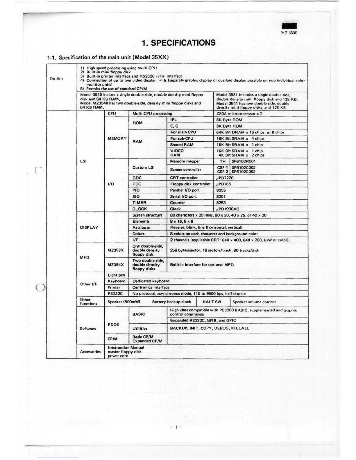
1.SPECIFICATIONS
1-1.
Specification
of the
main
unit
(Model 35XX)
Outline
1)
High
speed
processing
using multi-CPU
2)
Built-in
mini
floppy
disk
3)
Built-in
printer
interface
and
RS232C serial interface
4)
Connection
of up to two
Video displav
>nits
(separate
graphic display
or
overlaid
display
possible
on two
individual color
monitor
units)
5)
Permits
the use of
Standard CP/M
Model 3530
incluse a single double-side, double density
mini
floppy
disk
and 64 KB
RAM.
Model
MZ3540
has two
double-side, density
mini
floppy
disks
and
64 KB
RAM.
LSI
DISPLAY
MFD
Other
I/F
Other
functions
Software
Accessories
CPU
MEMORY
I/O
MZ353X
MZ354X
Light
pen
Keyboard
Printer
RS232C
Multi-CPU processing
ROM
RAM
Custom
LSI
GDC
FDC
RIO
SIO
TIMER
CLOCK
Screen
structure
Elements
Attribute
Colors
I/F
One
double-side.
double
density
floppy
disk
Two
double-side,
double
density
floppy
disks
IPL
C, G
For
main
CPU
For
sub-CPU
Shared
RAM
VIDEO
RAM
Memory mapper
Screen
Controller
CRT
Controller
Floppy
disk Controller
Parallel
I/O
port
Serial
I/O
port
Counter
Clock
Model 3531 includes a single
double-side,
double density
mini
floppy
disk
and 128 KB.
Model 3541
has two
double-side, double
density
mini
floppy
disks,
and 128 KB.
Z80A microprocessor
x 2
8K
Byte
ROM
8K
Byte
ROM
64K Bit
DRAM
x 16
Chips
or 8
Chips
16K Bit
SRAM
x 4
Chips
16K Bit
SRAM
x 1
Chip
16K Bit
SRAM
x 1
chip
4K Bit
SRAM
x 2
Chips
TH
SP6102R001
CSP-1
SP6102C002
CSP-2
SP6102C003
MPD7220
pPD765
8255
8251
8253
/JPD1990AC
80
characters
x 25
lines.
80 x 20, 40 x 25. or 40 x 20
8 x
16,8x8
Reverse,
blink,
line
(horizontal,
Vertical)
8
colors
on
each Character
and
background color
2
channels (applicable CRT:
640 x
400,
640 x
200,
B/W or
color).
256
bytes/sector,
16
sectors/track,
80
tracks/disk
Built-in
interface
for
optional
MFD.
Oedicated keyboard
Centronics interface
No
protocol.
asynchronus
mode,
110 to
9600
bps, half-duplex
Speaker
(500mW) Battery
backup
Clock
HALT
SW
Speaker
volume control
FDOS
CP/M
BASIC
Utilities
Basic
CP/M
Expanded CP/M
High
class
compatible
with
PC3200 BASIC, supplemented
and
graphic
control
commands
Expanded
RS232C,
GPIB,
and
GPIO
BACKUP,
INIT,
COPY, DEBUG.
KILLALL
Intstruction
Manual
master
floppy
disk
power
cord
O
Page 3
M Z 3500
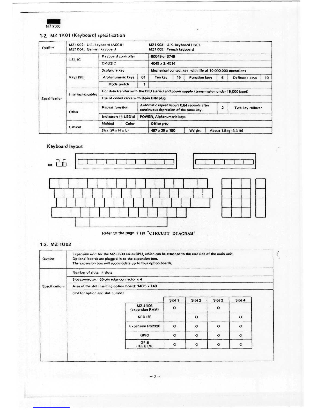
1-2.
MZ-1K01
(Keyboard)
specification
Outline
Specification
MZ1K02: U.S. keyboard (ASCII)
MZ1K03:
U.K. keyboard (ISO).
MZ1K04: Germankeyboard
MZ1K05:
French keyboard
LSI,
IC
Keys
(98)
Interfacing
cables
Other
Cabinet
Keyboard Controller
CMOSIC
Sculpture
key
Alphanumeric
keys
Mode switch
61
1
80C49
or
8749
4049x2,4514
Mechanical contact key,
with
life
of
10,000,000
operations.
Ten key
15
Function
keys
6
Definable keys
10
For
data transfer
with
the CPU
(serial)
and
power
supply
(transmission
under
15,000
baud)
Use
of
coiled
cable
with
8-pin
DIN
plug
Repeat
function
Indicators
(4
LED's)
Molded
Size
(W x H
Automatic
repeat
occurs
0.64 seconds after
....
, 2
Two-key rollover
contmuous depression
of the
same
key.
POWER,
Alphanumeric
keys
Color
xL)
Office
gray
467 x 35 x 190
Weight | About 1 .5kg
(3.3
Ib)
Keyboard
layout
Refer
to the
page
7 IN
"CIRCUIT
DIAGRAM"
1-3.
MZ-1U02
Outline
Specifications
Expansion
unit
for the
MZ-3500
series
CPU,
which
can be
attached
to the
rear side
of the
main
unit.
Optional
boards
are
plugged
in to the
expansion
box.
The
expansion
box
will
accomodate
up to
four
Option
boards.
Number
of
slots: 4 slots
Slot
connector:
60-pin
edge
connector
x 4
Area
of the
slot inserting
option
board:
140.5
x 140
Slot
for
Option
and
slot
number
MZ-1R06
(expansion RAM)
SFDI/F
Expansion RS232C
GPIO
GPIB
(IEEE
I/F)
Slot
1
O
O
o
o
Slot2
o
o
o
0
Slot
3
O
O
o
o
Slot
4
O
0
o
0
-2-
Page 4
MZ3500
Expansion
unit
Screw
(2)
Screw
(1)
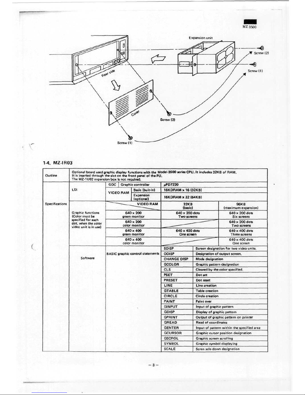
1-4. MZ-IR03
Outline
Specifications
Optional board
used
graphic display
functions
with
the
Model-3500
series
CPU.
It
includes 32KB
of
RAM.
It is
inserted
through
the
slot
on the
front
panel
of the PU.
The
MZ-1U02 expansion
box is not
required.
LSI
Graphic
functions
(Color
must
be
specified
for
each
dot. when
the
color
video
unit
is in
use)
Software
GDC
Graphic
Controller
Basic
(buit-in)
vinrn
RAM
-
Expansion
(optional)
-~-___WDEO
RAM
640 x 200
green
monitor
640 x 200
color
monitor
640
x 400
green
monitor
640 x 400
color
monitor
BASIC
graphic
control
Statements
MPD7220
16KDRAM
x 16
(32KB)
16KDRAM
x 32
(64KB)
32KB
(basic)
640 x 200
dots
Two
screens
______
—
- ~
640 x 400
dots
One
screen
___—
SDISP
ODISP
CHANCE DISP
GCOLOR
CLS
PSET
PRESET
LINE
GTABLE
CIRCLE
PAINT
GINPUT
GDISP
GPRINT
GREAD
GENTER
GCURSOR
GSCROL
SYMBOL
SCALE
96KB
(maximum expansion)
640 x 200
dots
Six
screens
640 x 200
dots
Two
screens
640 x 400
dots
Three
screens
640 x 400
dots
One
screen
Screen
designation
for two
video units.
Oesignation
of
Output
screen.
Mode designation
Graphic
pattern
designation
Cleared
by the
color specified.
Dot set
Oot
reset
Line
creation
Table creation
Circle creation
Paint over
Input
of
graphic pattern
Display
of
graphic pattern
Output
of
graphic pattern
on
printer
Read
of
coordinates
Input
of
pattern
within
the
specified
area
Graphic
Cursor
Position designation
Graphic
screen
scrolling
Graphic
symbol displaying
Seren
scle-down
designation
(
-3-
Page 5
M Z 3500
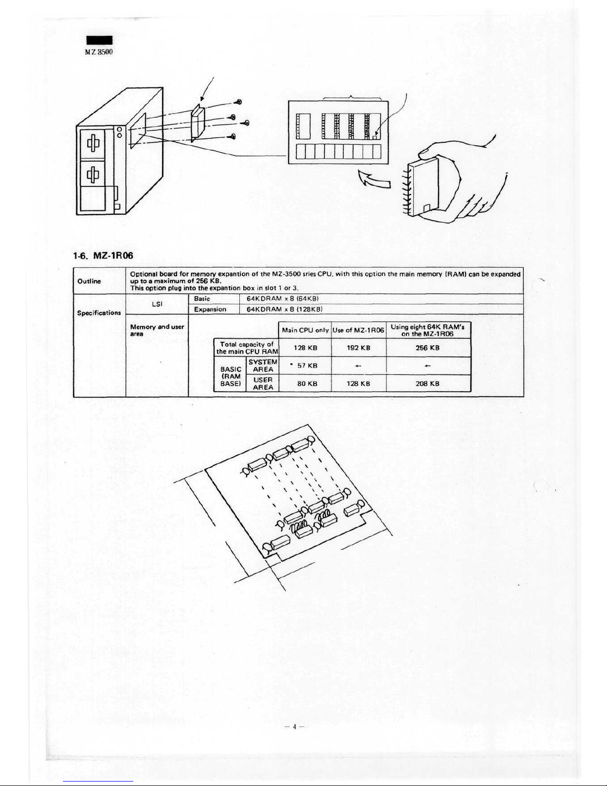
1-6.
MZ-1R06
Outline
Specifications
Optional board
for
memory expantion
of the
MZ-3500
sries
CPU. with this
Option
the
main memory (RAM)
can be
expanded
up to a
maximum
of 256 KB.
This
Option plug
into
the
expantion
box in
slot
1 or 3.
LSI
Memory
and
user
area
Basic
Expansion
64KDRAM
x 8
(64KB)
64KDRAM
x8
(128KB)
Total
capacity
of
the
main
CPU RAM
BASIC
(RAM
BASE)
SYSTEM
AREA
USER
AREA
Main
CPU
only
128 KB
• 57 KB
80 KB
Useof
MZ-1R06
192KB
-
128 KB
Using
eight
64K
RAM's
on
theMZ-1R06
256KB
-
208 KB
- 4 -
Page 6
MZ3500
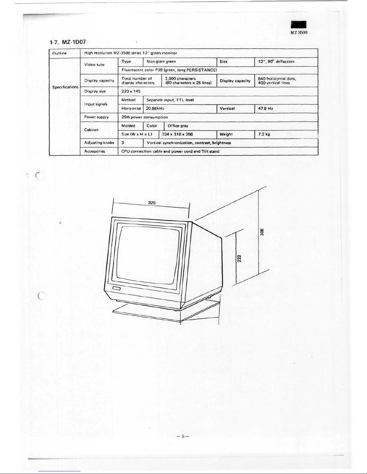
1-7.
MZ-1D07
Outline
Specifications
High
resolution
MZ-3500
series
12"
green
monitor
Video tube
Display capacity
Display
size
Input
Signals
Power supply
Cabinet
Adjusting
knobs
Accessories
Type
Non-glare green
Size
12".
90°
deflection
Fluorescent
color
P39
(green,
long
PERSISTANCE)
Total
number
of
display characters
2,000
characters
(80
characters
x 25
lines)
Display
capacity
640
horizontal
dots,
400
Vertical lines
220 x 145
Method
Horizontal
Separate
input,
TTL
level
20.86kHz
Vertical
47.8
Hz
29W
power
consumption
Molded
Color
Size
(W x H x L)
3
Office gray
324x310x356
Weight
7.2kg
Vertical
synchronization,
contrast,
brightness
CPU
connection
cable
and
power
cord
and Tut
stand
c
Page 7
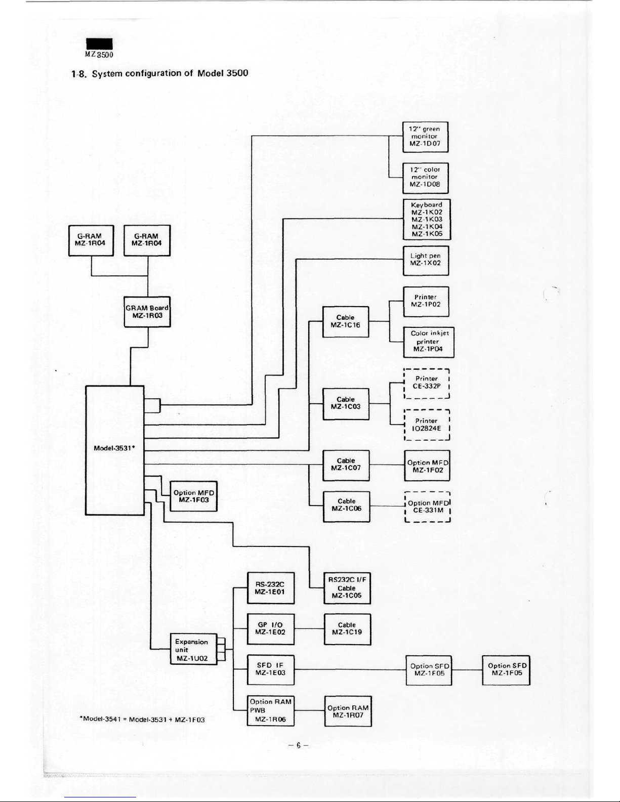
MZ3500
1-8.
System
configuration
of
Model 3500
Keyboard
M2-1K02
MZ-1K03
MZ-1K04
MZ-1K05
1
1
Printer
'
I02824E
l
|
l
Option MFDl
l
CE-331M
|
l l
*Model-3541 = Model-3531 + MZ-1F03
-6-
Page 8
M Z 3500
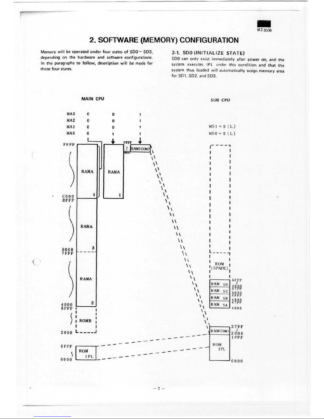
2.
SOFTWARE (MEMORY) CONFIGURATION
Memory
will
be
operated under
four
states
of
SDO ~ SD3,
depending
on the
hardware
and
Software
configurations.
In the
paragraphs
to
follow,
description
will
be
made
for
those
four
states.
2-1.
SDOUNITIALIZE STATE)
SDO
can
only
exist
immediately after power
on, and the
System
executes
IPL
under this
condition
and
that
the
system
thus loaded
will
automatically
assign
memory
area
for
SD1,
SD2,
and
SD3.
MAIN
CPU
SUB
CPU
MAS
MA2
MAI
MAO
17
p
171?
r
r r r
{
,
/
cooo
BFFF
]
/
8000
7
FFF
J
/
4000
3FFF
1
0
0
0
0
1
RAMA
4
RAMA
3
RAMA
2
1
1
ROMB
]
1
0
1
0 1
0 1
1 1
— 1 T
FFFF
T
] l
|RAM(COM)f
:nAn
1 i
tiOO
^\
\
RAMA
J 1
MSI
=0 (L)
MSO
= 0 (L)
2000
OFFF
0000
l
J
v
A
\\
\\
\\
U
\\
\\
\\
\\
\\
\\
ROM
(SPÄHE)
ROM
IPL
ROM
IPL
4000
2 7 FF
l
FFF
0000
Page 9
M Z 3500
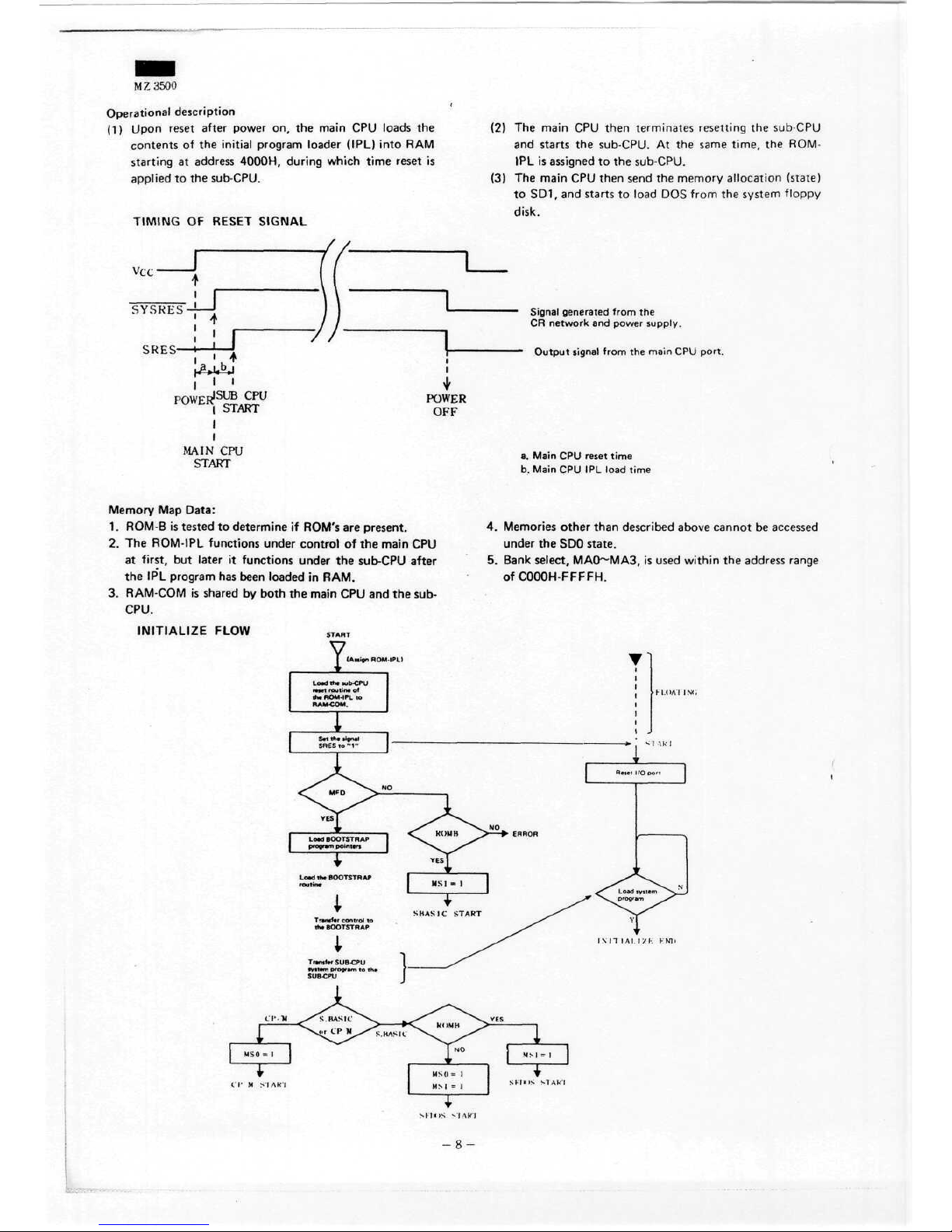
Operational
description
(1)
Upon
reset
after
power
on, the
main
CPU
loads
the
contents
of the
initial
program loader (IPL)
into
RAM
starting
at
address
4000H,
during
which
time
reset
is
applied
to the
sub-CPU.
TIMING
OF
RESET
SIGNAL
Vcc-
SYSRES-
SRES-
•*
I
l
pnwFR
ISUB
CPU
P°*E
*<
START
l
l
POWER
OFF
(2) The
main
CPU
then
terminates
resetting
the
sub-CPU
and
Starts
the
sub-CPU.
At the
same
time,
the
ROM-
IPL is
assigned
to the
sub-CPU.
(3) The
main
CPU
then send
the
memory allocation
(state)
to
SD1.
and
Starts
to
load
DOS
from
the
System
floppy
disk.
Signal
generated
from
the
CR
network
and
power
supply.
Output
Signal
from
the
main
CPU
port.
MAIN
CPU
START
a.
Main
CPU
reset
time
b.
Main
CPU IPL
load
time
Memory
Map
Data:
1.
ROM-B
is
tested
to
determine
if
ROM's
are
present.
2. The
ROM-IPL
functions
under
control
of the
main
CPU
at
first,
but
later
it
functions
under
the
sub-CPU
after
the IPL
program
has
been
loaded
in
RAM.
3.
RAM-COM
is
shared
by
both
the
main
CPU and the
sub-
CPU.
INITIALIZE
FLOW
4.
Memories
other
than
described above
cannot
be
accessed
under
the SDO
state.
5.
Bank select,
MAO~MA3,
is
used
within
the
address
ränge
ofCOOOH-FFFFH.
-
Page 10
ROM IPL
1. An 8KB ROM
(2764
or
mask
ROM
equivalent)
is
used
for the
ROM-IPL.
2.
When
the
system
reset
signal turns
from
Iow to
high
state
after
power
on, the
main
CPU
Starts
to
operate.
At
this stage,
the
ROM-IPL
is
addressed.
3. The CPU
Starts
from
address
0000(ROM
address
10000).
4. The
main
CPU
sets
the
sub-CPU
reset
signal
from
Iow to
high
state
äs
itgoes
out of its
initial
state
via the
memory
mapper
and the
sub-CPU
Starts
to
operate.
At
this
point,
the
ROM-IPL
is
addressed
by the
sub-CPU.
5.
Address
0000
of the
sub-CPU
is ROM
address
(0000).
The
memory
area above
ROM
address
(1000)
cannot
be
used
by the
sub-CPU because
the
main
CPU
initial
program
has
been loaded
there.
'
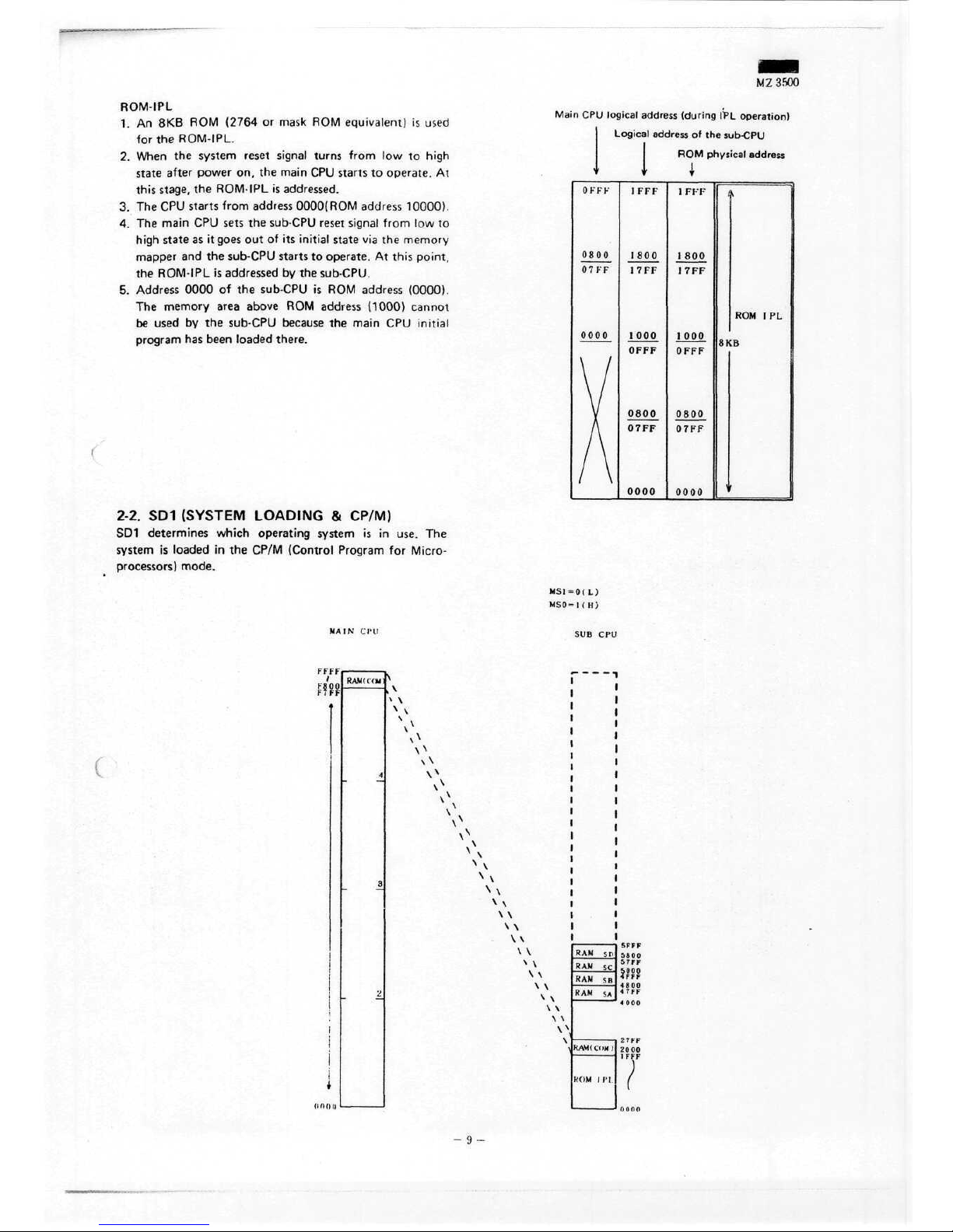
2-2.
SD1
(SYSTEM
LOADING & CP/M)
SD1
determines
which
operating
system
is in
use.
The
system
is
loaded
in the
CP/M
(Control
Program
for
Micro-
processors)
mode.
MZ3500
Main
CPU
logical
address
(during
IPL
Operation)
Logical
address
of the
sub-CPU
I
ROM
physical
address
i
OFFF
0800
07
FF
0000
X
V
1
FFF
1
800
17
FF
1
000
OFFF
0800
07FF
0000
1
FFF
1
800
17FF
1
000
OFFF
0800
07FF
0000
8F
\
'
ROM IPL
.B
MS1=0(L)
WSO=1(H)
SUB
CPU
r r r r
/
F7
(
FF
; 'i f i ( i
RAM
(KM
4
3
k
\
»
\
x
\
V
- 9 -
Page 11
M Z
3500
Operational
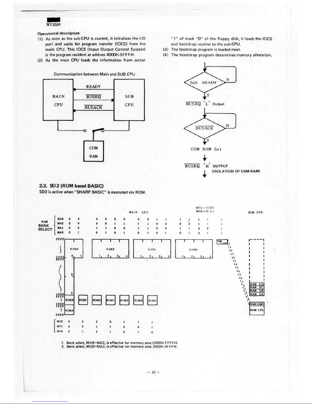
description
(1)
As
soon
äs the
sub-CPU
is
started,
it
initializes
the I/O
port
and
waits
for
program transfer (IOCS)
from
the
main
CPU.
This
IOCS
(Input
Output
Control
System)
is
the
program resident
at
address
4000H-5FFFH.
(2)
As the
main
CPU
loads
the
Information
from
sector
Communication between Main
and SU B CPU
"1" of
track
"0" of the
floppy
disk,
it
loads
the
IOCS
and
bootstrap routine
to the
sub-CPU.
(3) The
bootstrap program
is
loaded next.
(4)
The
bootstrap program determines memory allocation.
BUSRQ H OUTPUT
l
(ISOLATION
OF COM
RAM)
2.3.
SD 2
(ROM
based
BASIC)
SD2
is
active
when
"SHARP
BASIC"
is
executed
via
ROM.
MAIN
CI'U
MS]
= l (H)
MSO
= 0; L;
SUB CPU
MA3
RAM
BANK
MAI
SELECT
MAI
MAO
FFFF
cooo
4000
im
0000
{MO2
00
0000
00
0011
00
1100
01
0101
1
III
RAMA
RAMB
4
3
2
ROM
B
ROMA
0
1
1,2,3,4
ROMC ROMU
ROM]
ROM2
000]
MO]
00110
MOO
01010
0
1
I
0
1
'l
0 1 1
I
0 0
I
0 0
1
0 1
1 1
HAM<_
2, 3, 4
1111
0 0 1 1
1100
0101
1 1 1
KAMI.
l| 2, S| 4
]
1
1
1
püS >
LZLrnm
v V
\\
\\
\\
U
u
\\
u
\\
u
H
1»
»\
v\
°v
RAM
SD
RAM
SC
RAM
SB
RAM
SA
1.
Bank
select.
MAO~MA3.
is
effective
for
memory
area
COOOH-FFFFH.
2.
Bank
select.
MOO~MA2,
is
effective
for
memory
area
2000H-3FFFH.
Page 12
M.Z
3500
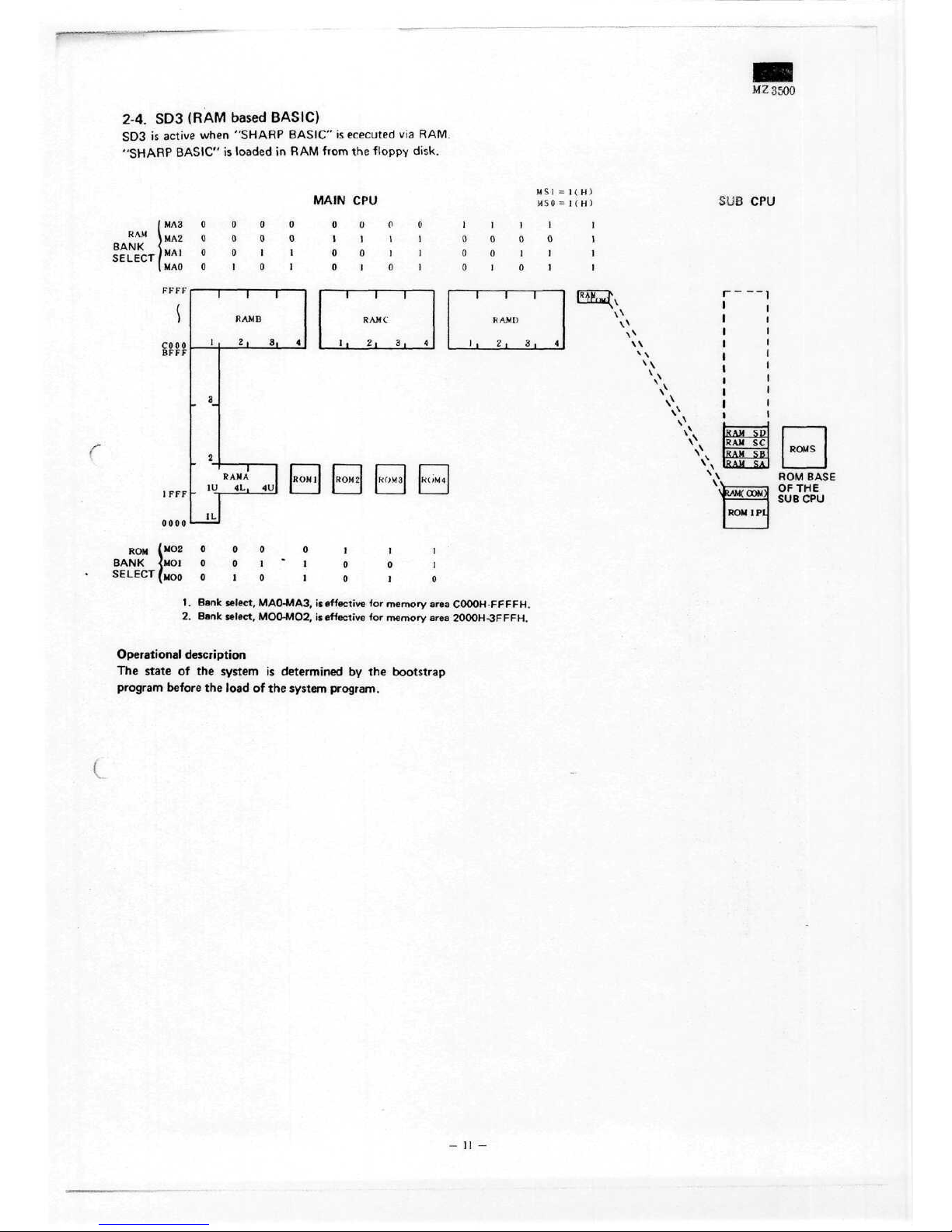
2-4.
SD3
(RAM based BASIC)
SD3 is
active
when
"SHARP BASIC"
is
ececuted
via
RAM.
"SHARP BASIC"
is
loaded
in RAM
from
the
floppy disk.
MAIN
CPU
MSI
=
1<H)
SUB CPU
RAM
BANK
SELECT
MA3
0000 0000
1111
1
MA
10011
0011 0011
1
MAO
0101 0101 0101
1
(
)
SFF?
1FFF
0000
III III III
lüftaJx
" '
RAMB
RAMC
RAM»
x
\
\^
1
2,3,4
1,2,3,4
1,2,3,4
\\
3_
L
2
^\
^\
V
*
0
\\
RAJt|
SP
\\
RAM
SC
V, RAM SB
KOMo
RAMA
ROMl
ROM2 KOW3 ROM4
\\ ROM BAS
1L
"-•
"u S'WfOOM)
Ut
" '"
C
ROM
1 Pl
ROM
(«02
0 0 0 0 l 1 1
BANK <M01
0 0 1 " 1 0 0 1
SELECT (
MOO
010 10 I 0
1.
Bank select, MAO-MA3,
is
effective
for
memory
area COOOH-FFFFH.
2.
Bank select. MOO-MO2,
is
effective
for
memory
area
2000H-3FFFH.
Operational description
The
state
of the
System
is
determined
by the
bootstrap
program
before
the
load
of the
System
program.
Page 13
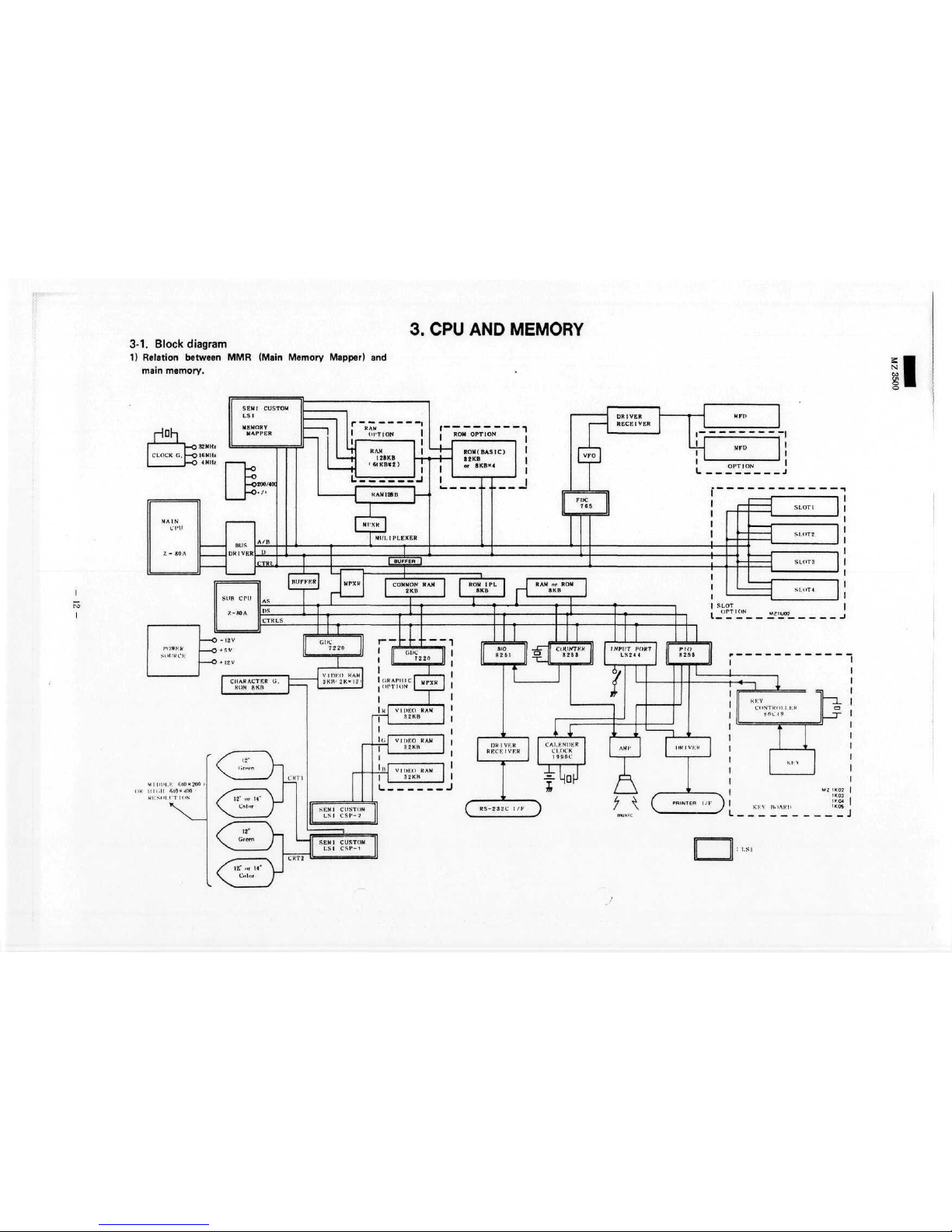
3-1. Block
diagram
1)
Relation between
MMR
(Main Memory Mapper)
and
main memory.
3. CPU AND
MEMORY
Höh
PH
CLOCK
('..
—O 32 MI!
—O
ISMHi
—O
4Mll>
MAIN
CI'U
7.
- 80 A
SEMI
CUSTOM
LSI
MEMORY
MAPPER
-0
-o
-O
200/4«
-O./.
=
Sl
BUS
DK1VKR
=====
B CPU
/-80A
A/B
U
CTRL]
||AS
m
P^—
—
l
1
,
r-„-
r
FKER
II 1 1
T"
RAM |
<64KB»2)
'
1
1
1
MI'XH
MDL
IPLEXER
pou
OPTION
U_ m
MPXK
COMMON
RAM
2KB
1
!•
ROM ( BAS
I C ) 1
S2KB
1
or
«KBX4
1
L
i
V
F
=
K
76
=
ROM
IPL 1 RAM or ROM
8KB
[~~|
8KB
1 - 1
r—
RECEIVER
L LL
MFD
i
-o
1 ' 1
.
OPTION
'
f
P
. II
SLOT1
SI.OTZ
SLOT3
SLOT
4
n
^T 1 ON
MZIUO?
yinni.i:
OK
H n.n
V V T
PRINTER
l/K J
l
Page 14
M Z 3500
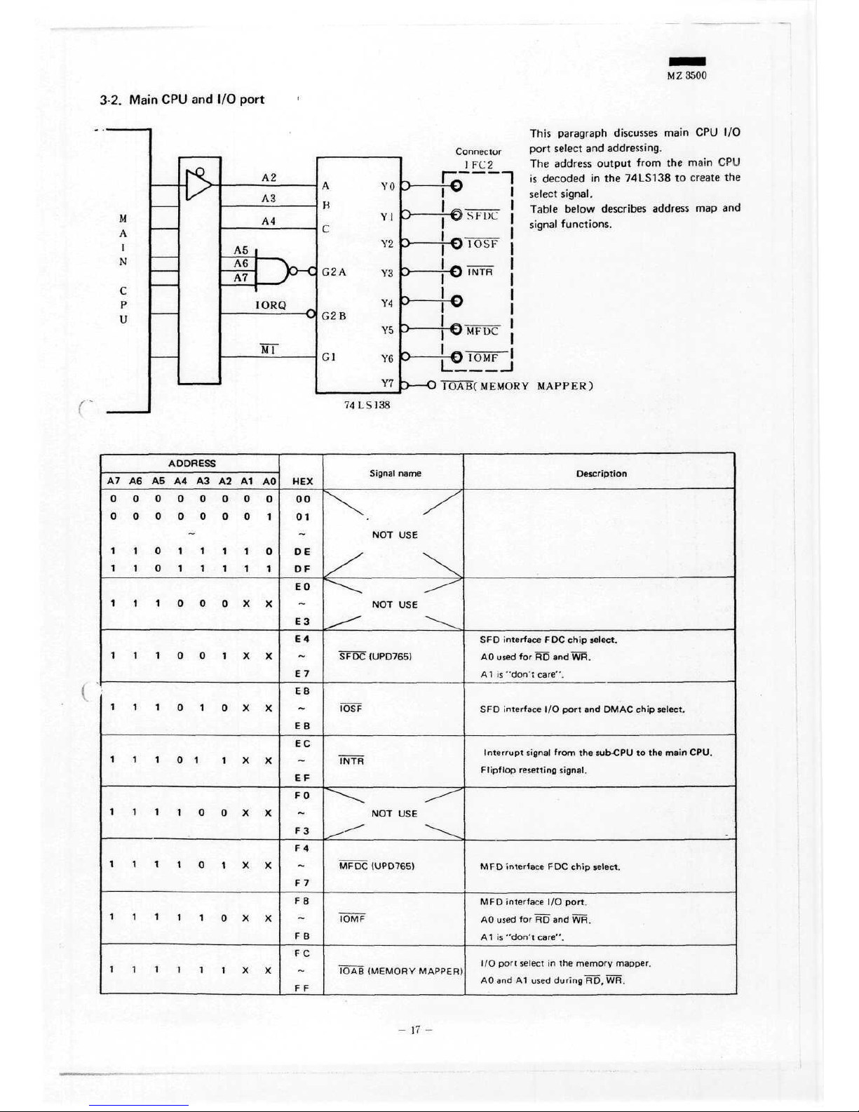
3-2.
Main
CPU and I/O
port
M
A
I
N
C
P
U
[NO
Ix
A2
A3
A4
A5
i
A6
"A
V\
r
A7
P
C
IORQ
MT
A YO
Y 1
Oi A Y3
Y4
G2
B
Y5
Gl Y6
74LS138
This
paragra
Connector
Port
select
an
1
FC2 The
address
_
\~f\
~~\ is
decoded
it
v
select
signal.
T f^i
-,-,.,-
Table
below
^ v#
."> r L)C
signal
functic
J
V
J
0
MFÜC
0 T"O
IOMF
L
|
3
U
IOABCMEMORY
MAPPER)
ADDRESS
A7
A6 A5 A4 A3 A2 A1 AO
00000000
00000001
11011110
11011111
1 1 1 0 0 0 X X
t'\-\OQ1XX
^t'\OtOXX
11101
1 X X
1111QOXX
1 1 1 1 0 1 X X
1 1 1 1 1 0 X X
1 1 1 1 1 1 X X
HEX
00
01
DE
DF
EO
E3
E4
E
7
E8
EB
EC
EF
FO
F3
F4
F7
F8
F
B
FC
F F
NOT USE
NOT USE
SFDC
(UPD765)
IOSF
INTR
NOT USE
MFDC
(UPD765)
IOMF
IOAB
(MEMORY
MAPPER)
SPD
interface
FDC
chip
select.
AO
used
for RD and WR.
A1 is
"don' t care".
SPD
interface
I/O
port
and
DMAC chip select.
!
Interrupt
signal
from
the
sub-CPU
to the
main
CPU.
i
Flipflop
resetting
signal.
MFD
interface
FDC
chip
select.
MFD
interface
I/O
port.
AO
used
for RD and WR.
AI is
"don't
care".
I/O
port
select
in the
memory
mapper
AOand
A1
used
during
RD, WR.
Page 15
MZ3500
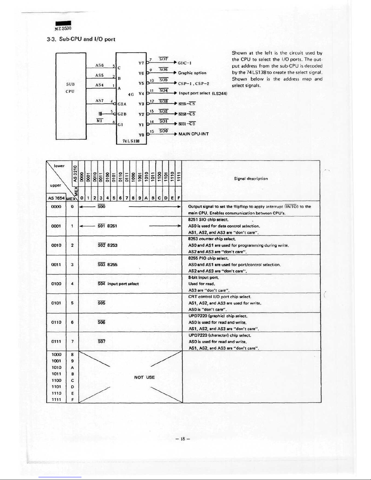
3-3.
Sub CPU and I/O
port
SUB
CPU
AS6 5
ASS
2
AS4
i
AS7
4^
5
*Ü~
6
Y6
4G
Y4
Gl
Yl
YO
74LS138
„7
S07
t
Ä
9 506
^IQ
SO5 ^
J ^
CSP
1 ,
CSP
2
^11 SO4 -
-12
SÖ3" ^ -JTTT
D15 SÖ2"
HEC3
"C"-
14
SÖT —
D
"H^
MAIN
CPU-INT
Shown
at the
left
is the
Circuit
used
by
the CPU to
Select
the I/O
ports.
The
out-
put
address
from
the sub CPU is
decoded
by the
74LS138to
create
the
Select
signal.
Shown
below
is the
address
map and
select
Signals.
AS
7654 MEX\
8
8
1
23456789A8CDEF
8
8
Signal
description
0000
SOO
Output
signal
to set the
flipflop
to
apply
Interrupt (INTO)
to the
main CPU.
Enable:
communication
between CPU's.
0001
S01
8251
8251
SIO
Chip Select.
ASO
is
used
for
data
control
selection.
AS1,
AS2,
and ASS are
"don't care".
0010
S02
8253
8253 counter
chip
Select.
ASO
and AS1 are
used
for
Programming
during write.
AS2
and ASS are
"don't
care".
0011
S03
8255
8255
PIO
Chip
select.
ASO
and AS1 are
used
for
port/control
selection.
AS2
and ASS are
"don't
care".
0100
S04
input
port
Select
8-bit
input
port.
Used
for
read.
AS3
are
"don't
care".
0101
CRT
control
I/O
port
chip select.
AS1, AS2,
and ASS are
used
for
write.
ASO
is
"don't
care".
0110
S06
UPD7220
(graphic)
chip
select.
ASO
is
used
for
read
and
write.
AS1, AS2,
and ASS are
"don't
care"
0111
SÜ7
UPD7220
(Character)
chip
select.
ASO
is
used
for
read
and
write.
AS1, AS2,
and AS3 are
"don't
care"
1000
1001
1010
1011
1100
1101
1110
1111
NOT USE
-
18-
Page 16
MZ3500
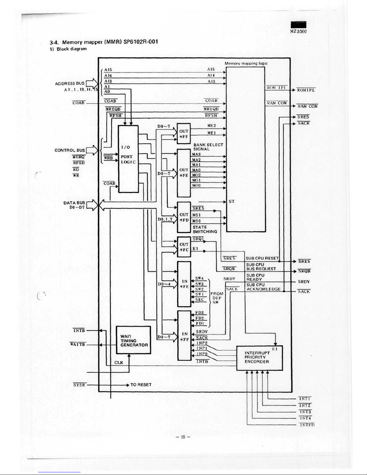
3-4. Memory mapper (MMR) SP6102R-001
1)
Block
diagram
ADDRESS
BUS[
J)
AO
. l
.13.14?1S
CÜAB
CONTROL
BUS
MERQ
RFSH
RD
DATA
BUS
DO-D7
oc
INTB
WAITB
SYSR
A15
A14
AI3
AI
AO
COAB
MREQB
RFSH
Memory
A 15
AI4
RB
GAB
1/0
PORT
LOGIC
~L
""L
1
-
WAIT
TIMING
GENERATOR
CLK
TORESET
INTERRUPT
PRIORITY
ENCORDER
I
NTFI)
19
-
Page 17
M Z 3500
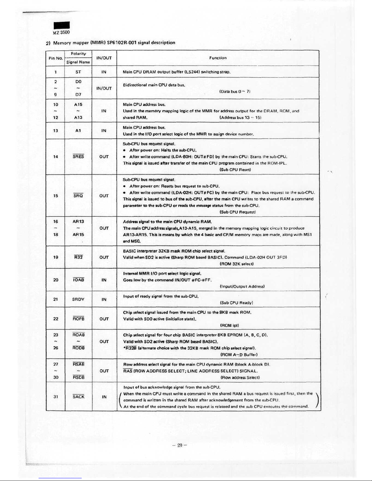
2)
Memory
mapper
(MMR)
SP6102R-001
signal
description
1
2
9
10
12
13
14
15
16
18
19
20
21
22
23
26
27
~
30
31
Polarity
Signal
Name
ST
DO
D7
A15
A13
A1
SRES
SRQ
AR13
AR15
R32
IOAB
SRDY
ROPB
ROAB
RODB
RSAB
~
RSDB
SACK
IN
IN/OUT
IN
IN
OUT
OUT
OUT
OUT
IN
IN
OUT
OUT
OUT
IN
Main
CPU
DRAM Output buffer
(LS244)
switching
strap.
Bidirectional main
CPU
data bus.
(Data
bus 0 ~ 7)
Main
CPU
address
bus.
Used
in the
memory mapping logic
of the MMR for
address
Output
for the
DRAM, ROM,
and
shared
RAM. (Address
bus 13 ~ 15)
Main
CPU
address
bus.
Used
in the I/O
port
Select
logic
of the MMR to
assign
device
number.
Sub-CPU
bus
request
signal.
•
After
power
on:
Halts
the
sub-CPU.
•
After
write
command
(LDA-80H: OUT#FD)
by the
main CPU:
Starts
the
sub-CPU.
This signal
is
issued after transfer
of the
main
CPU
program contained
in the
ROM-IPL.
(Sub
CPU
Reset)
Sub-CPU
bus
request
signal.
•
After power
on:
Resets
bus
request
to
sub-CPU.
•
After write command
(LDA-02H:
OUT#FC)
by the
main CPU:
Place
bus
request
to the
sub-CPU.
This
signal
is
issued
to bus of the
sub-CPU, after
the
main
CPU
writes
to the
shared
RAM a
command
Parameter
to the
sub-CPU
or
reads
the
message
Status
from
the
sub-CPU.
(Sub
CPU
Request)
Address
signal
to the
main
CPU
dynamic RAM.
The
main
CPU
address signals,A13-A
15,
merged
in the
memory mapping logic
Circuit
to
produce
AR13-AR15.
This
is
means
by
which
the 4
basic
and
CP/M memory
maps
are
made.
along
with
MS1
and
MSO.
BASIC
interpreter
32KB mask
ROM
chip
Select
signal.
Valid
when
SD2 is
active (Sharp
ROM
based BASIC). Command (LDA
02H OUT
3FD)
(ROM
32K
Select)
Internal
MMR I/O
port
select
logic
Signal.
Goes
Iow by the
command
IN/OUT
#FC-#FF.
(Input/Output
Address)
Input
of
ready
signal
from
the
sub-CPU.
(Sub
CPU
Ready)
Chip select signal issued
from
the
main
CPU to the 8KB
mask
ROM.
Valid
with
SDO
active
(initialize
state).
(ROM
ipl)
Chip
select signal
for
four
chip
BASIC interpreter
8KB
EPROM
(A. B. C, D).
Valid
with
SD2
active (Sharp
ROM
based
BASIC).
*R32B (alternate choice
with
the
32KB
mask
ROM
chip
select signal).
(ROM
A~D
Buffer)
Row
address
Select
Signal
for the
main
CPU
dynamic
RAM
(block A-block
D).
RAS
(ROW ADDRESS SELECT; LINE
ADDRESS
SELECT)
SIGNAL.
(Row
address
Select)
Input
of bus
acknowledge
signal
from
the
sub-CPU.
command
is
Written
in the
shared
RAM
after
acknowledgement from
the
sub-CPU.
l
At the end of the
command
cycle
bus
request
is
released
and the sub CPU
executes
the
command.
/
-
20-
Page 18
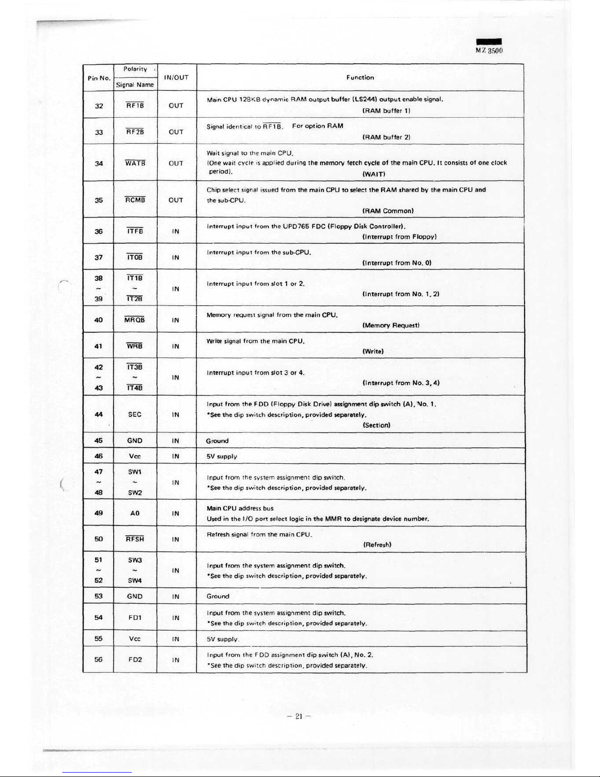
M 7,
3500
Pin
No.
32
33
34
35
36
37
38
39
40
41
42
43
44
45
46
47
48
49
SO
51
52
53
54
55
56
Polarity
:
Signal
Name
RF1B
RF2B
WATB
RCMB
ITFB
ITOB
IT1B
IT2B
MRQB
WRB
IT3B
TT4B
SEC
GND
Vcc
SW1
SW2
AO
RFSH
SW3
SW4
GND
FD1
Vcc
FD2
IN/OUT
OUT
OUT
OUT
OUT
IN
IN
IN
IN
IN
IN
IN
IN
IN
IN
IN
IN
IN
IN
IN
IN
IN
Function
Main
CPU
128KB
dynamic
RAM
Output
buffer
(LS244)
Output
enable
signal.
(RAM
buffer
1)
Signal
identical
to R F 1 B. For
Option
RAM
(RAM buffer
2)
Wait
signal
to the
main CPU.
(One
wait
cycle
is
applied during
the
memory
fetch cycle
of the
main
CPU.
It
consists
of one
clock
period). (WAIT)
Chip
Select
signal
issued
from
the
main
CPU to
Select
the RAM
shared
by the
main
CPU and
the
sub-CPU.
(RAM
Common)
Interrupt
input
from
the
UPD765
FDC
(Floppy
Disk
Controller).
(Interrupt
from
Floppy)
Interrupt
input
from
the
sub-CPU.
(Interrupt
from
No. 0)
Interrupt
input
from slot
1 or 2.
(Interrupt
from
No. 1, 2)
Memory
reguest
signal
from
the
main CPU.
(Memory Request)
Write
signal
from
the
main CPU.
(Write)
Interrupt
input
from slot
3 or 4.
(Interrupt
from
No. 3, 4)
Input
from
the FDD
(Floppy
Disk Drive) assignment
dip
switch
(A).
No. 1.
'See
the dip
switch
description,
provided
separately.
(Section)
Ground
5V
supply
Input
from
the
System
assignment
dip
switch.
•See
the dip
switch description.
provided
separately.
Main
CPU
address
bus
Used
in the I/O
port
Select
logic
in the MMR to
designate device
number.
Refresh
signal
from
the
main CPU.
(Refresh)
Input
from
the
system
assignment
dip
switch.
'See
the dip
switch
description,
provided
separately.
Ground
Input
from
the
System
assignment
dip
switch.
'See
the dip
swuch description,
provided
separately.
5V
supply.
Input
from
the F DO
assignment
dip
switch (A),
N o. 2.
*See
the dip
switch
description, provided
separately.
-
2l
-
-
.-..,,,..,
Page 19
M
7,3500
Pin
No.
57
58
59
60
61
62
63
64
65
66
67
68
69
70
71
72
73
Polarity
Signal
Name
SYSR
FD3
COAB
RO1B
GND
Vcc
RO2B
RÖ3B
'ROB
CLK
RO4B
MPX
GND
CASB
GND
INTB
IN/OUT
IN
IN
IN
OUT
IN
IN
OUT
IN
OUT
OUT
IN
OUT
IN
OUT
Function
System
reset
Signal.
Used
to
reset
I/O
port
in the
MMR.
(System
Reset)
Input
from
the
sytem
assignment
dip
switch.
'See
the dip
switch description, provided
separately.
Shared
RAM
Select
Signal.
Address
of the
shared
RAM is
*F800-#FFFF
for the
main
CPU
(Common
RAM
Address)
Select
Signal
for 8KB
area
allocated
to
slot
1.
Valid
when
SD2 is
active (ROM
based
BASIC)
and SD3
(RAM
based
BASIC).
(ROM
1)
Ground
5V
supply
Select
signal
for 8KB
area
allocated
to
slot
2 or 3
Valid
when
SD2 is
active (ROM
based
BASIC)
and SD3
(RAM
based
BASIC).
(ROM2.
3)
Read
signal from
the
main CPU.
(Read)
EAIT signal generation
Clock.
(Clock)
Select
signal
for 8KB
area
allocated
to
slot
4.
Valid
when
SD2 or SD3
(RAM
based BASIC)
are
active.
(ROM
4)
RAS/CAS
address
switching signal
for the
main
CPU
DRAM.
High:
Row
address
Low:
Column
address
(Multiplex)
Ground
CAS
(Column
Address) signal
for the
main
CPU 64K
DRAM.
•Refresh
for the RAM
only.
(Column
Address
Select
Buffer)
Ground
' l h •
(Interrupt)
Not
used
-22-
Page 20
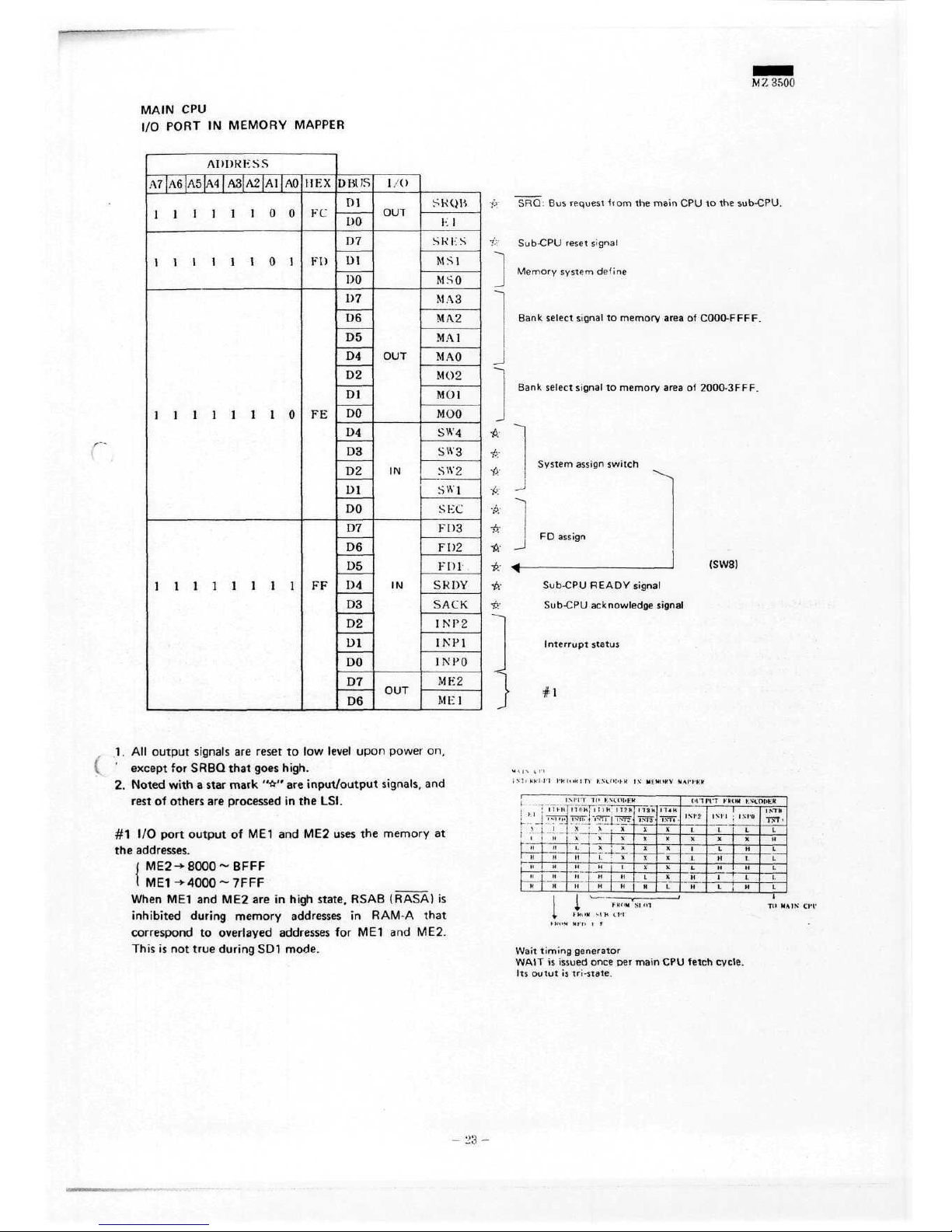
M Z 3500
MAIN
CPU
I/O
PORT
IN
MEMORY
MAPPER
ADDRESS
A7|A6|A5|A4|A3|A2|Al|AO
11111101
11111110
11111111
II
EX
U f~
KI)
FE
FF
UHUS
Dl
00
D7
ül
DO
1)7
D6
D5
D4
D2
Dl
DO
D4
D3
D2
Dl
DO
D7
D6
D5
1)4
D3
D2
Dl
DO
D7
D6
I/O
OUT
IN
IN
SKQH
i-;
i
S K K S
MSI
MSO
M
A3
MA2
MAI
MAO
MO2
MOI
MÜO
S\\'4
swg
SW2
swi
SHC
FD
3
FD2
FD1
SKDY
SACK
INP2
INT1
INFO
ME2
M
El
-•->
SRQ:
Bus
request
Irom
the
main
CPU to the
sub-CPU.
7-V
Sub-CPU
reset
signal
Memory
System
define
Bank select signal
to
memory
area
of
COOO-FFFF.
,J
•A
Bank
select
Signal
to
memory
area
of
2000-3FFF.
System
assign
switch
FD
assign
(SW8)
•fr
Sub-CPU READY signal
•fr
Sub-CPU acknowledge
signal
Interrupt
Status
.1.
All
Output
Signals
are
reset
to Iow
level
upon
power
on,
l
except
for
SRBQ
that
goes
high.
2.
Noted
with a star
mark
"6" are
Input/Output
Signals,
and
rest
of
others
are
processed
in the
LSI.
#1 I/O
port
Output
of ME1 and ME2
uses
the
memory
at
the
addresses.
ME2->8000~BFFF
ME1->-4000~7FFF
When
ME1 and ME2 are in
high
state,
RSAB (RASA)
is
inhibited
during
memory
addresses
in
RAM-A
that
correspond
to
overlayed addresses
for ME1 and
ME2.
This
is not
true
during
SD1
mode.
; 1 1 )• ii
.il'lLI
-iq-r-j
H 1 H
II 1 H
H j H
i
MTT Td f.
r
i n
H"T"i
1 1 h
Tvr7T.J
'i'vfr
"l4-
M [ 1.
H J H
" i "
H
t»
i "-
i-
ki
IM
M>
i
«U
»Ft.
1
72h
ITSL
K
X
'
H
"
Y
fHOH
i
r'
1
13h
•Jvn
X
X
X
X
L
H
si
m
inh
/
on
IM'2
1
X
1.
L
H
H
Cl'T
K K
-T"
X
L
K
H
.
L
»M
t-M
IM'O
L
X
H
I
H
L
H
11
IKK
IM h
Tvf>
L
II
L
L
L
l
L
1
TO Vf
Wait
timing
generator
WAIT
is
issued once
per
main
CPU
fetch
cycle.
Its
outut
is
tri-state.
-
L>3
-
Page 21
MZ3500
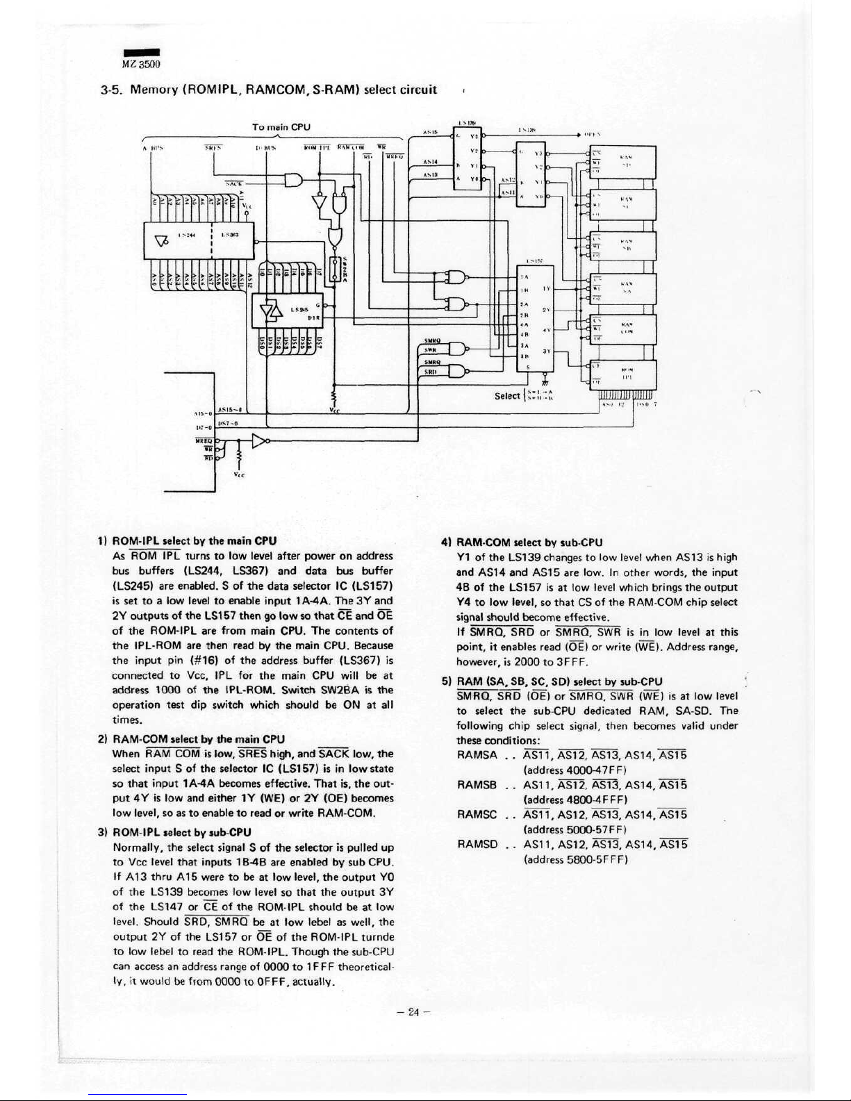
3-5.
Memory
(ROMIPL,
RAMCOM,
S-RAM) Select
Circuit
To
main
CPU
1)
ROM-IPL
Select
by the
main
CPU
As
ROM IPL
turns
to Iow
level after power
on
address
bus
buffers (LS244, LS367)
and
data
bus
buffer
(LS245)
are
enabled.
S of the
data selector
IC
(LS157)
is
set to a Iow
level
to
enable
input
1A-4A.
The 3Y and
2Y
Outputs
of the
LS157
then
go Iow so
that
CE and ÖE
of the
ROM-IPL
are
from
main
CPU.
The
Contents
of
the
IPL-ROM
are
then
read
by the
main
CPU. Because
the
input
pin
(#16)
of the
address
buffer
(LS367)
is
connected
to
Vcc,
IPL for the
main
CPU
will
be at
address 1000
of the
IPL-ROM.
Switch
SW2BA
is the
Operation test
dip
switch
which
should
be ON at all
times.
2)
RAM-COM
Select
by the
main
CPU
When
RAM COM is
Iow, SRES
high,
and
SACK Iow,
the
Select
input
S of the
selector
IC
(LSI
57) is in
Iowstate
so
that
input
1A-4A becomes
effective.
That
is, the
out-
put 4Y is Iow and
either
1Y
(WE)
or 2Y
(OE) becomes
Iow
level,
so äs to
enable
to
read
or
write
RAM-COM.
3)
ROM-IPL
Select
by
sub-CPU
Normally,
the
Select
signal
S of the
selector
is
pulled
up
to Vcc
level
that
inputs
1B-4B
are
enabled
by sub
CPU.
If A13
thru
A15
were
to be at Iow
level,
the
Output
YO
of the
LS139 becomes
Iow
level
so
that
the
Output
3Y
of the
LS147
or CE of the
ROM-IPL
should
be at Iow
level.
Should SRD, SMRQ
be at Iow
lebel
äs
well,
the
Output
2Y of the
LS157
or 51 of the
ROM-IPL
turnde
to Iow
lebel
to
read
the
ROM-IPL.
Though
the
sub-CPU
can
access
an
address
ränge
of
0000
to
1FFF theoretical-
ly, it
would
be
from
0000
to
OFFF,
actually.
4)
RAM-COM
Select
by
sub-CPU
Y1 of the
LS139
changes
to Iow
level
when AS13
is
high
and
AS14
and
AS15
are
Iow.
In
other words,
the
input
4B of the
LS157
is at Iow
level
which
brings
the
Output
Y4 to Iow
level,
so
that
CS of the
RAM-COM
chip
select
signal
should
become
effective.
If
SMRQ,
SRD or
SMRQ,
SWR is in Iow
level
at
this
point,
it
enables read (OE)
or
write (WE). Address ränge,
however,
is
2000
to
3FFF.
5) RAM
(SA,
SB. SC, SD)
Select
by
sub-CPU
SMRQ,
SRD
(ÖT)
or
SMRQ,
SWR
(WE)
is at Iow
level
to
select
the
sub-CPU dedicated RAM, SA-SD.
The
following
chip
select
signal, then becomes valid under
these
conditions:
RAMSA
..
AS11, ÄS12, AS13, AS14, AS15
(address
4000-47FF)
RAMSB
..
AS11.ÄST2,
ÄS~T3,
AS14, ÄS15
(address
4800-4FFF)
RAMSC
..
AS11, AS12, AS13, ASM. AS15
(address
5000-57FF)
RAMSD
..
AS11, AS12,
ÄSl3,
AS14,
(address
5800-5FFF)
-
24
-
Page 22
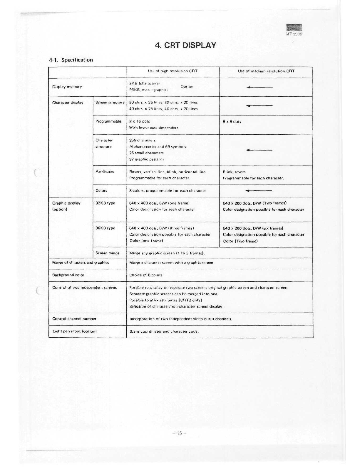
4. CRT
DISPLAY
V 3i 30
4-1.
Specification
Use
of
high resolution
CRT
Display
mernory
Character display
Graphic
display
(option)
Screen
structure
Programmable
Character
structure
Attributes
Colors
32KB
type
96KB
type
Screen
merge
Merge
of
chracters
and
graphics
Background
Color
Control
of two
independent
screens
Control
channel
number
Light
pen
input
(option)
3KB
(Character;)
Option
96KB.
max.
(graphic
l
80
chrs.
x 25
Imes,
80
chrs.
x 20
lines
40
chrs.
x 25
Imes.
40
chrs.
x 20
Imes
8x16 dots
With
Iower
case
descenders
255
characters
Alphanumerics
and 69
Symbols
26
small
characters
97
graphic
patterns
Revers,
Vertical
line.
blink,
horizontal
line
Programmable
for
each Character.
8
colors,
Programmable
for
each Character
640 x 400
dots.
B/W
(one frame)
Color
designation
for
each
Character
640 x 400
dots.
B/W
(three frames)
Color
designation possible
for
each Character
Color
(one frame)
Use
of
medium
resolution
CRT
8x8
dots
Blink,
revers
Programmable
for
each Character.
640 x 200
dots,
B/W
(Two
frames)
Color
designation
possible
for
each Character
640 x 200
dots.
B/W
(six frames)
Color
designation
possible
for
each Character
Color
(Two
frame)
Merge
any
graphic screen
(1 to 3
frames).
Merge a Character screen
with a graphic
screen.
Choice
of 8
colors
Possible
to
d'bplay
on
separate
two
screens
original
graphic
scieen
and
Character screen.
Separate
graphjc
screens
can be
merged
into
one.
Possible
to
affix
attributes
(CRT2
only)
Selection
of
Character
/non-character screen
display.
Incorporation
of two
independent Video
outut
channels.
Scans
coordinates
and
Character
code.
Page 23
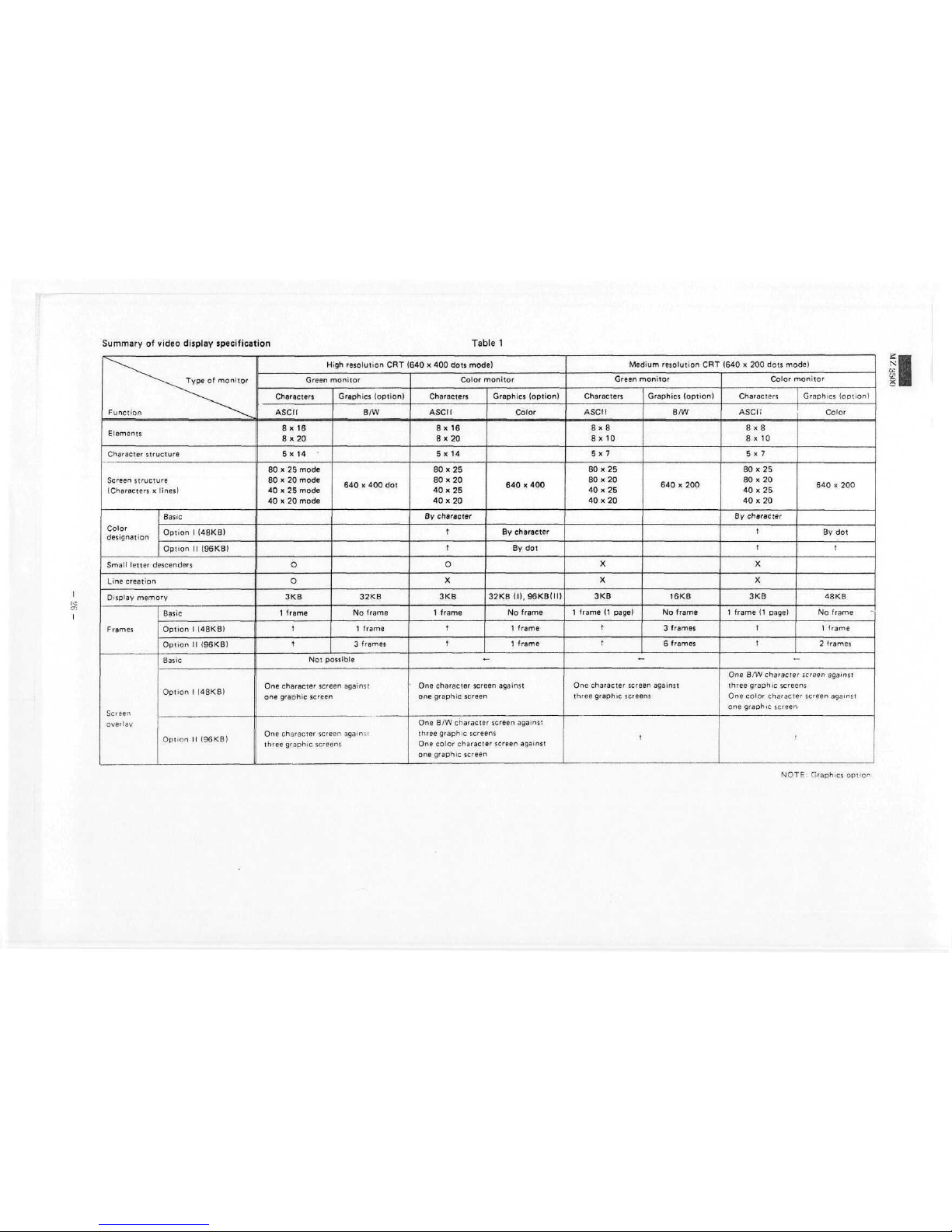
Summary
of
video
display specification
Table
1
^^^^^
Type
of
monitor
Function
^^^^
Elements
Character structure
Screen
structure
(Characters x ines)
Color
designation
Basic
Option 1 (48KB)
Option
II
(96KBI
Small letter descenders
Line
creation
Display
memory
Frames
Screen
overlay
Basic
Option 1 (48KB)
Option
II
(96KB)
Basic
Option 1 (48KB)
Option
II
196KB)
High
resolution
CRT
(640
x 400
dots
mode)
Green
monitor
Characters
ASCII
8x 16
8x20
5x 14
80 x 25
mode
80 x 20
mode
40 x 25
mode
40 x 20
mode
O
O
3KB
1
frame
t
t
Graphics
(option)
B
/W
640 x 400 dot
32KB
No
frame
1
frame
3
frames
Not
possible
One
Character
screen
against
one
graDhic
screen
One
Character
screen
ngamsi
three
graphic
screens
Color
monitor
Characters
ASCII
8x 16
8x 20
5x 14
80 x 25
80 x 20
40 x 25
40 x 20
By
Character
t
t
O
X
3KB
1
frame
t
t
Graphics
(option)
Color
640 x 400
By
Character
By
dot
32KB
(I),96KB(II)
No
frame
1
frame
1
frame
«-
One
Character
screen against
one
graphic screen
One B/W
Character
screen
against
three graphic
screens
One
color
Character
screen
against
one
graphic screen
Medium
resolution
CRT
(640
x 200
dots
mode)
Green
monitor
Characters
ASCII
8x8
8x10
5x7
80 x 25
80 x 20
40 x 25
40
x20
X
X
3KB
1
frame
(1
page)
t
t
Graphics
(option)
B /W
640 x 200
16KB
No
frame
3
frames
6
frames
*-
One
Character
screen
against
three graphic screens
Color
monitor
Characters
ASCI:
8x8
8x10
5x7
80 x 25
80 x 20
40 x 25
40 x 20
By
Character
t
1
X
X
3KB
1
frame
(1
page)
t
t
Graphics
(option)
Color
640 x 200
By
dot
t
48KB
No
frame
1
frame
2
frames
-
One B/W
Character screen agamst
three graphic
screens
One
Color
Character
screen
agamst
one
graphic
screer,
!
I
l
IC
er.
NOTE:
Graphics
option
Page 24
M Z 3500
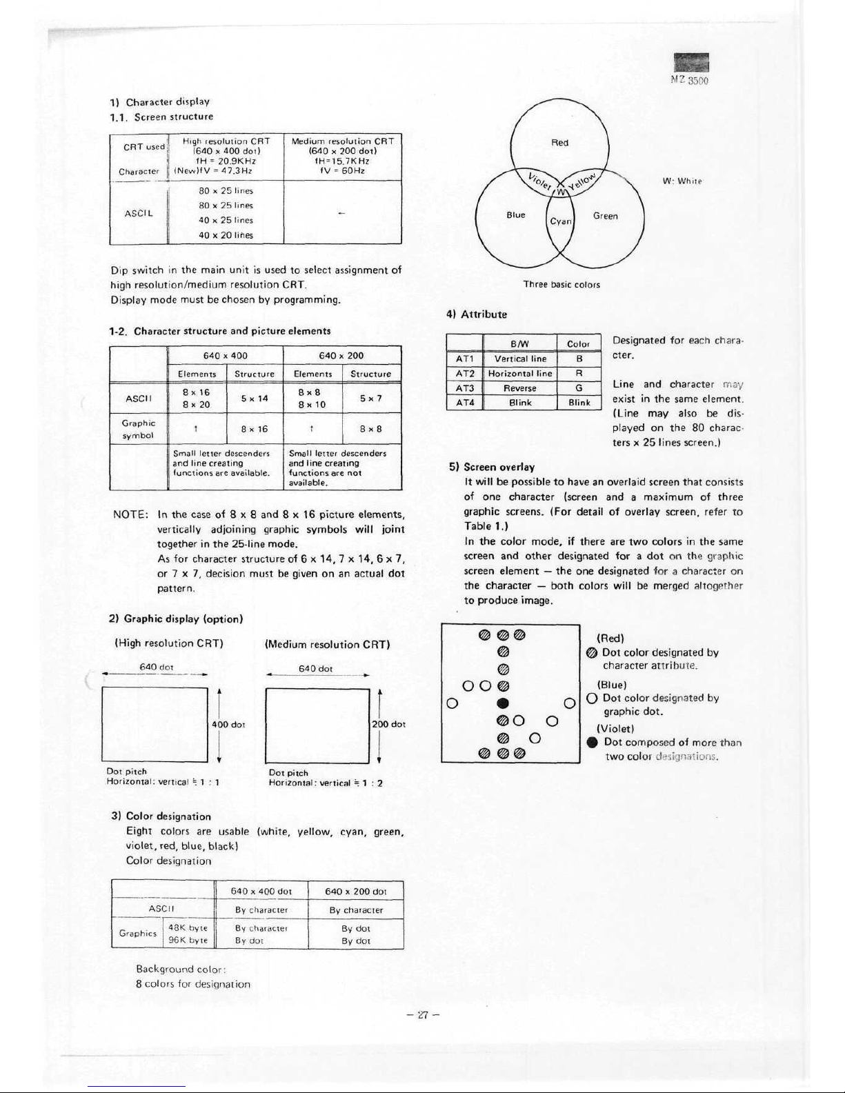
1}
Character display
1.1.
Screen
structure
CRT
used
Character
ASCII
High
resolution
CRT
(640
x 400
dot)
fH • 20.9KHz
(New)fV = 47.3
Hz
80 x 25
lines
80 x 25
lines
40 x 25
lines
40 x 20
lines
Medium
resolution
CRT
(640
x 200
dol)
fH =
15.7KHz
fV =
60Hz
-
Dip
switch
in the
main
unit
is
used
to
Select
assignment
of
high resolution/medium resolution CRT.
Display
mode must
be
chosen
by
Programming.
1-2.
Character
structure
and
picture elements
ASCII
Graphic
Symbol
640 x 400
Elements
8x 16
8x 20
1
Structure
5 x 14
8x 16
Small
letter
descenders
and
line
creating
functions
are
avaitable.
640 x 200
Elements
8x8
8 x 10
t
Structure
5x7
8x8
Small
letter
descenders
and
line
creating
functions
are not
available.
NOTE:
In the
case
of 8 x 8 and
8x16
picture
elements,
vertically
adjoining graphic Symbols
will
joint
together
in the
25-line
mode.
As
for
Character
structure
of 6 x 14, 7 x 14,
6x7,
or
7 x 7,
decision must
be
given
on an
actual
dot
pattern.
2)
Graphic
display
(option)
(High
resolution
CRT)
640 dot
(Medium
resolution
CRT)
640 dot
400 dot
200
dot
Dot
pitch
Horizontal:
Vertical
= 1:1
Dot
pitch
Horizontal:
Vertical
= 1:2
W:
White
Three
basic
colors
4)
Attribute
AT1
AT2
ATS
AT4
B/W
Vertical
line
Horizontal
line
Reverse
Blink
Color
B
R
G
Blink
Designated
for
each
Chara-
cter.
Line
and
Character
rr.üy
exist
in the
same
element.
(Line
may
also
be
dis-
played
on the 80
charac-
ters
x 25
lines
screen.)
5)
Screen overlay
It
will
be
possible
to
have
an
overlaid
screen
that
consists
of one
Character (screen
and a
maximum
of
three
graphic
screens.
(For
detail
of
overlay screen,
refer
to
Table
1.)
In the
color
mode,
if
there
are two
colors
in the
same
screen
and
other
designated
for a dot on the
graphic
screen
element
— the one
designated
for a
Character
on
the
Character — both
colors
will
be
merged
altogpTher
to
produce
Image.
00
o
o
>o
o
»
o
(Red)
© Dot
color
designated
by
Character
attribute.
(Blue)
O Dot
color
designated
by
graphic dot.
(Violet)
£ Dot
composed
of
more than
two
color
designntions.
3)
Color
designation
Eight
colors
are
usable
(white,
yellow,
cyan, green,
violet,
red,
blue,
black)
Color
designation
ASCII
_
48K
hyte
Graphics
| 96 K
byte
640 x 400 dot
By
Character
By
Character
By
dot
640 x 200 dot
By
Character
By
dot
By
dot
Background
color:
8
colors
for
designation
Page 25
M Z 3500
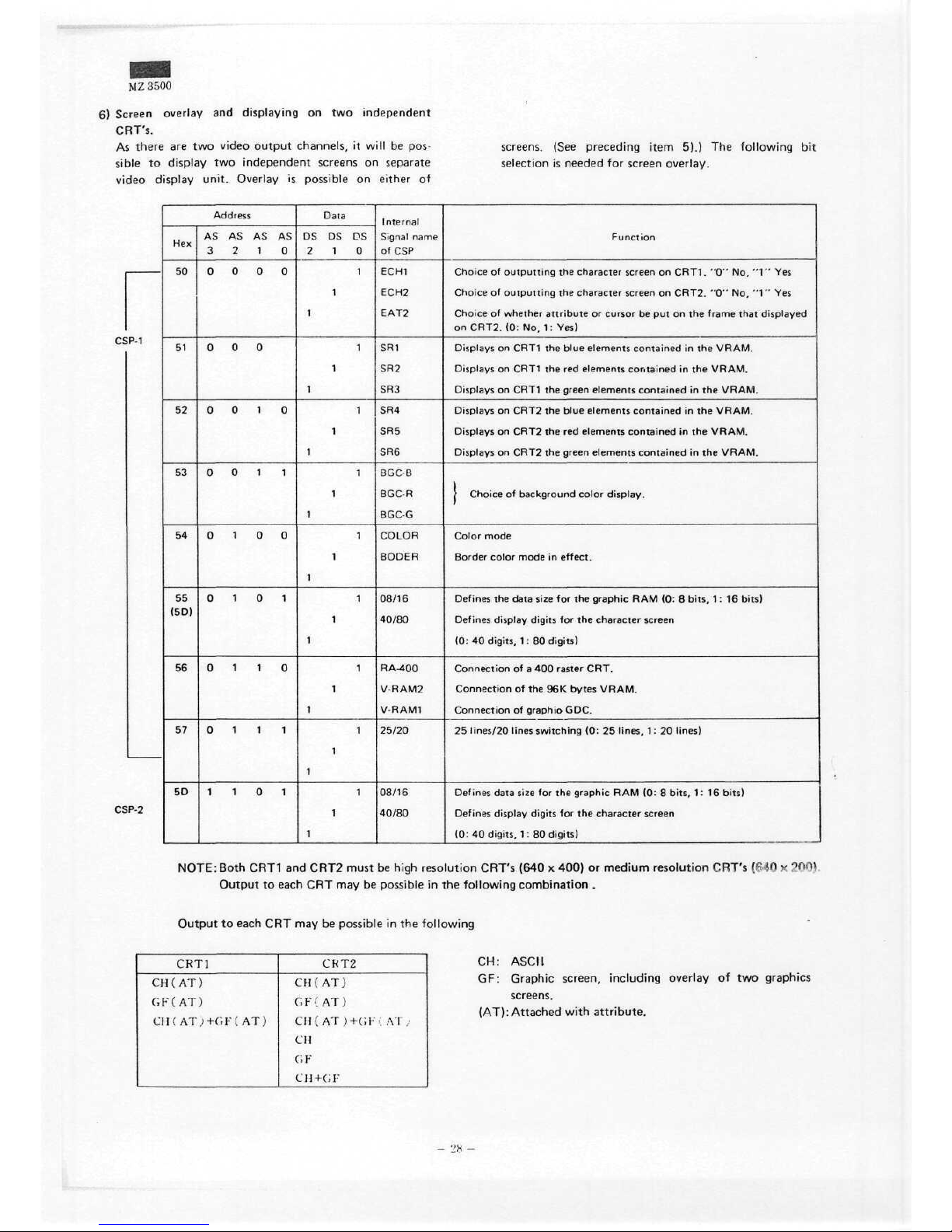
6)
Screen
overlay
and
displaying
on two
independent
CRT's.
As
there
are two
video
Output
channels,
it
will
be
pos-
sible
to
display
two
independent
screens
on
separate
video
display
unit.
Overlay
is
possible
on
either
of
screens.
(See
preceding
item
5).)
The
following
bit
selection
is
needed
for
screen
overlay.
;p-i
;p-2
Address
Hex
50
51
52
53
54
55
(50)
56
57
5D
AS AS AS AS
3210
0000
000
0010
0011
0100
0101
0110
0111
1101
Data
DS
DS DS
2 1 0
1
1
1
1
1
1
1
1
1
1
1
1
1
1
1
1
1
1
1
1
1
1
1
1
1
1
1
Internal
Signal
name
of CSP
ECH1
ECH2
EAT2
SR1
SR2
SR3
SR4
SR5
SR6
BGC-B
BGC-R
BGC-G
COLOR
BODER
08/16
40/80
RA-400
V-RAM2
V-RAM1
25/20
08/16
40/80
Function
Choice
of
outputting
the
Character
screen
on
CRT1.
"0" No, "1" Yes
Choice
of
outputting
the
Character
screen
on
CRT2.
"0" No, "1 " Yes
Choice
of
whether
attribute
or
Cursor
be put on the
frame that displayed
on
CRT2.
(0: No, 1:
Yes)
Displays
on
CRT1
the
blue elements contained
in the
VRAM.
Displays
on
CRT1
the red
elements contained
in the
VRAM.
Displays
on
CRT1
the
green elements contained
in the
VRAM.
Displays
on
CRT2
the
blue elements contained
in the
VRAM.
Displays
on
CRT2
the red
elements
contained
in the
VRAM.
Displays
on
CRT2
the
green elements contained
in the
VRAM.
/
Choice
of
background
Color
display.
Color mode
Border color mode
in
effect.
Defines
the
data
size
for the
graphic
RAM (0: 8
bits,
1:16 bits)
Defines
display digits
for the
Character screen
(0:
40
digits,
1 : 80
digits)
Connection
of a 400
raster CRT.
Connection
of the 96K
bytes
VRAM.
Connection
of
graphio GDC.
25
lines/20 lines switching
(0: 25
lines,
1 : 20
lines)
Defines
data
size
for the
graphic
RAM (0: 8
bits,
1: 16
bits)
Defines
display digits
for the
Character
screen
(0:
40
digits,
1 : 80
digits)
NOTE:Both
CRT1
and
CRT2
must
be
high
resolution
CRT's
(640 x 400)
or
medium
resolution
CRT's
(640 x 200>
Output
to
each
CRT may be
possible
in the
following
combination
.
Output
to
each
CRT may be
possible
in the
following
CRT1
CH
( AT )
GF(AT)
CH ( AT
.)+r,F(
AT)
CKT2
CH(AT)
GF(
AT)
cn( AT
)-K;F>,
AT .
CH
GF
CH+GF
CH:
ASCII
GF:
Graphic
screen,
including
overlay
of two
graphics
screens.
(AT):Attached
with
attribute.
Page 26
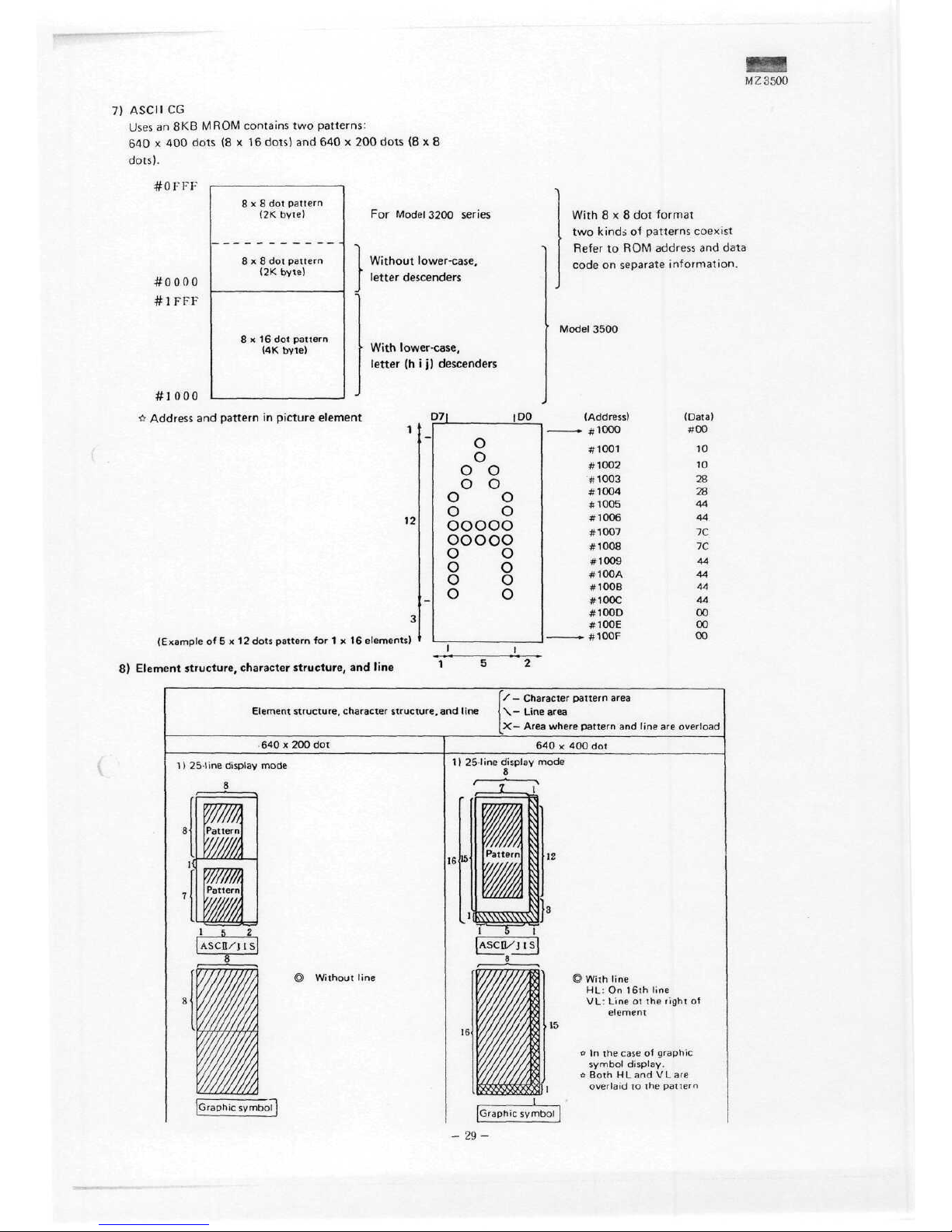
7)
ASCII
CG
Uses
an 8KB M ROM
contains
two
patterns:
640 x 400
dots
(8x16
dots)
and 640 x 200
dots
(8x8
dots).
M Z 3500
-H-
u r r r
#0000
#1FFF
#1 onn
8x8 dot
pattern
(2K
byte)
8x8 dot
pattern
(2K
byte)
8x16
dot
pattern
(4 K byte)
For
Model
3200
series
With
8x8 dot
formal
two
kindi
of
patterns
coexist
~\
Without
Iower-case,
letter
descenders
>
With
Iower-case,
letter
(h i j)
descenders
Address
and
pattern
in
picture
element
D7| |DO
1
12
/F*amnlp
nf fi x 12
dots
nattern
for
1x16 elements)
_
O
o
o
o
o
o
^*s ^-S
o o
o
o
ooooo
ooooo
o o
0
0
o o
o o
Refer
to ROM
address
and
data
code
on
separate
Information.
Model
3500
(Address)
(Data)
.
#1000
#00
#1001
10
#1002
10
#1003
28
#1004
28
#1005
44
#1006
44
#1007
7C
#1008
7C
#1009
44
#100A
44
#100B
44
#100C
44
#100D
00
#100E
00
~
#100F
00
8)
Element
structure,
Character
structure,
and
line
Element
structure,
Character
structure,
and
line
/—
Character
pattern
area
\—
Line area
X—
Area where pattern
and
line
are
overload
640x200
dot
1)
25-line
display
mode
fil
Iflf:
Pattern
'A
Pattern
l 5 2
IASCD/JIS]
Without
line
[(^raphic
symbolj
640 x 400 dot
1)
25-line
display
mode
8
16
12
Ascn/jis
©With
line
HL: On
16th line
VL:
Line
ot the
right
of
element
o In the
case
of
graphic
Symbol
display.
e
Both
HL and VL are
overlaid
to the
pattern
l
Graphic
symbol
i
-
29-
Page 27
M ^ 3500
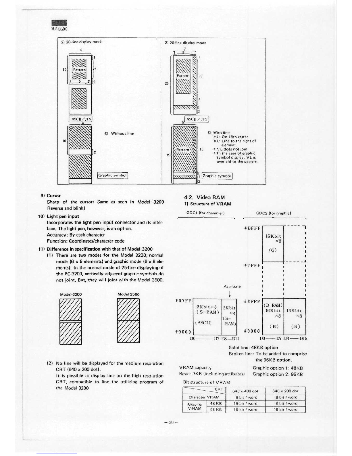
2)
20-line display
mode
10
Without
line
Graphic
Symbol
2)
20-line display
mode
8
20«
20
XXSNNX^-ll
With
line
HL: On
18th
raster
VL:
Line
to the
right
of
element
c
V L
does
not
join
0 In the
case
of
graphic
Symbol
display,
VL is
overlaid
to the
pattern.
Graphic Symbol
|
9)
Cursor
Sharp
of the
Cursor: Same
äs
seen
in
Model
3200
Reverse
and
blink)
10)
Light
pen
input
Incorporates
the
light
pen
input
connector
and its
inter-
face.
The
light
pen, however,
is an
Option.
Accuracy:
By
each
Character
Function:
Coordinates/character code
11)
Difference
in
specification
with
that
of
Model
3200
(1)
There
are two
modes
for the
Model
3200;
normal
mode (6x9 elements)
and
graphic mode (6x8 ele-
ments).
In the
normal mode
of
25-line displaying
of
the
PC-3200, vertically adjacent graphic symbols
do
not
joint.
But, they
will
joint
with
the
Model 3500.
Model-3200
Model
3500
(2)
No
line
will
be
displayed
for the
medium resolution
CRT
(640
x 200
dot).
It is
possible
to
display line
on the
high resolution
CRT,
compatible
to
line
the
utilizing program
of
the
Model 3200
4-2.
Video
RAM
1)
Structure
of
VRAM
GDC1 (for Character)
GDC2
(for graphic)
#BFFF
*7FFF
16Kbit
(G)
Attribute
#07FF
#0000
2Kbit
*8
(
S -R
AM)
(ASCI
L
2Kbit
x4
(S-
RAM)
#3FFF
#0000
(D-RAM)
16Kbit
xS
(B)
16Kbit
x8
(R)
DO-
-D7
D8—DU
DO-
-D7
D8-
-D15
Solid
line:
48KB
Option
Broken
line:
To be
added
to
comprise
the
96KB
Option.
VRAM
capacity
Graphic
Option
1:
48KB
Basic:
3KB
(including
attibutes)
Graphic
Option
2:
96KB
Bit
Structure
of
VRAM
— — £^J
640x400
dot
Character
VRAM
Graphic l 48KB
V-RAM
j
96 KB
j
8 bit /
word
16
bit /
word
16 b<t /
word
640
x 200 de i
8
bit /
word
8 bit /
word
16
bit /
word
-
30-
Page 28
M Z 3500
2)
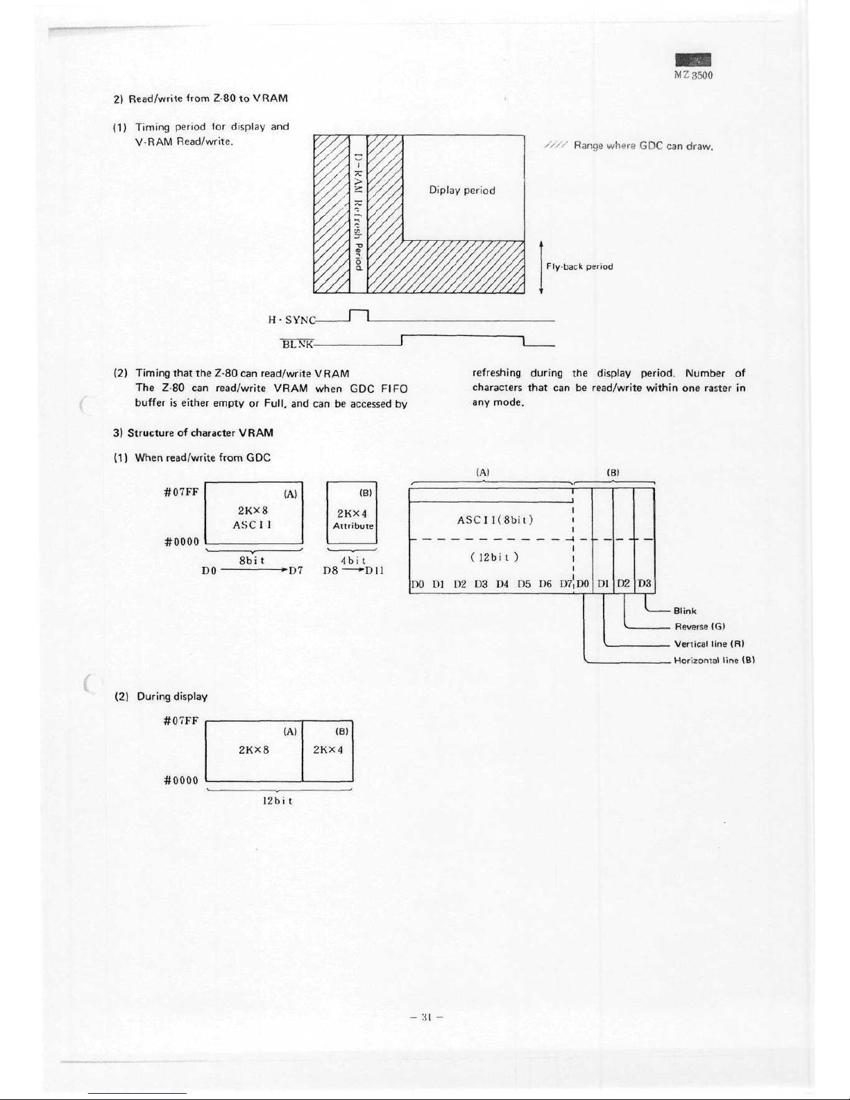
Read/write from 2-80
to
VRAM
(1)
Timing
period
for
display
and
V-RAM
Read/write.
Diplay
period
////
Range
whers
GDC can
draw.
Fly-back
period
H •
SYNC-
BLNK-
(2)
Timing
that
the
Z-80
can
read/write VRAM
The
Z-80
can
read/write VRAM when
GDC
FIFO
buffer
is
either empty
or
Füll,
and can be
accessed
by
3)
Structure
of
Character
VRAM
(1)
When read/write
from
GDC
#07
FF
#0000
refreshing
during
the
display
period.
Number
of
characters
that
can be
read/write
within
one
raster
in
any
mode.
(A)
(B)
(A)
2KX8
ASCI
I
8bi t
30 * D i
(B)
2KX4
Attribute
4bi
t
)ö * U
l
1
ASClKSbit)
i
i
_ — — — __ — —
__i-
l
(12bit)
i
DO
Dl D2 D3 D4 D5 D6
D7|D
0
D
1D2
D3
L
Blink
Vertical
line
(R)
Horizontal
line
(B)
(2)
During
display
#07FF
#0000
(A)
2KX8
(B)
2KX4
,
12bi
t
Page 29
M 2 3500
4)
Graphic
VRAM
memory
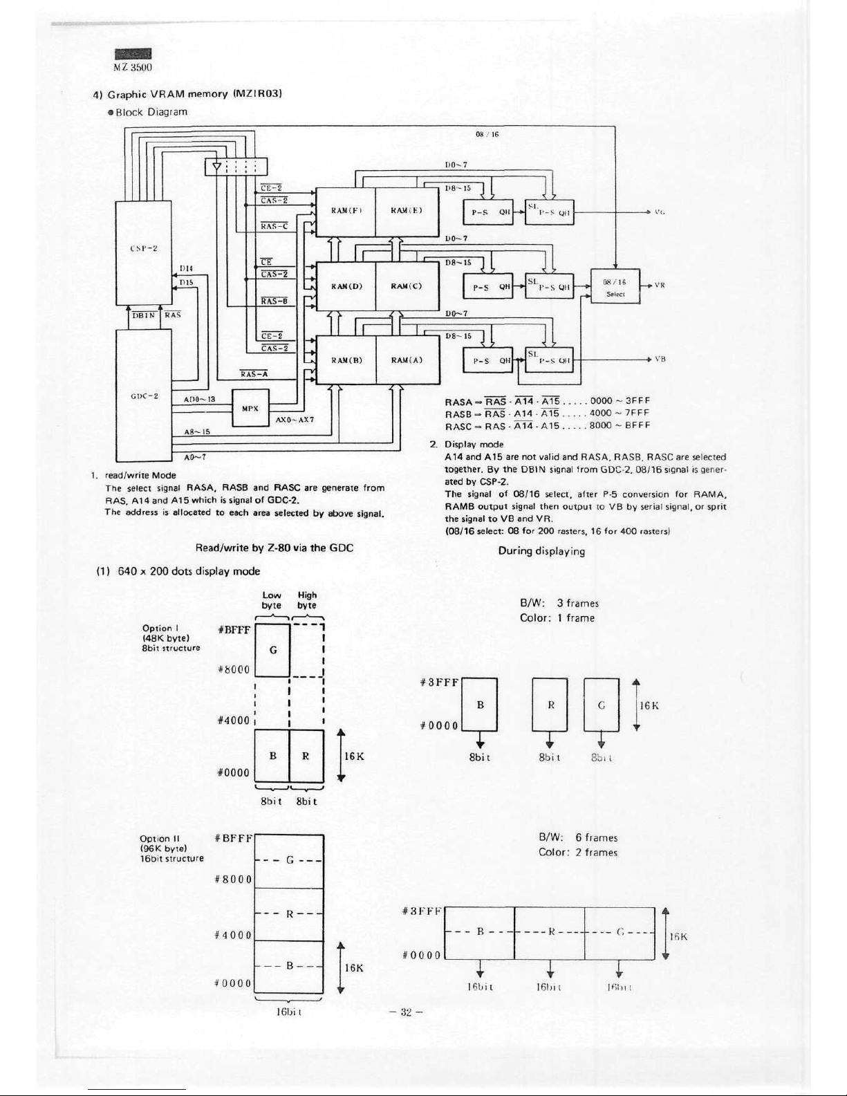
(MZIR03)
•
Block
Diagram
t+r-
1
CSP-8
D14
CAS-2
RAM'.FI
RAMCK)
M
1
1 Ir—
RAM(D)
RAW(C)
1 1
|
RAM(B)
RAM(A)
i
n
P-S QH
T
\[
SL
I'-S
A8-15
AO—7
1.
read/write Mode
The
select
signal
RASA, RASB
and
RASC
are
generate
from
RAS,
A14 and A1 5
which
is
signal
of
GDC-2.
The
address
is
allocated
to
each
area
selected
by
above
signal.
Read/write
by
Z-80
via the GDC
(1)
640 x 200
dots
display
mode
Option l #BFFF
(48K
byte)
8bit
structure
#8000
#4000
#0000
Low
byte
G
B
High
byte
-
__
i
R
i
16K
RASA
= RAS • A14 • A15 . .
RASB=
RAS • A14 • A15 .
RASC
=• RAS • A14 • A15 . .
.
. .
0000 ~ 3FFF
.
. .
4000
~ 7 F F F
. . 8000 ~ BFFF
2.
Display mode
A14 and A15 are not
valid
and
RASA, RASB. RASC
are
selected
together.
By the
DBIN
signal
from
GDC-2. 08/16 signal
is
gener-
ated
by
CSP-2.
The
signal
of
08/16
Select,
after
P-5
conversion
for
RAMA,
R
AM B
Output signal then Output
to V B by
Serial
signal,
or
sprit
the
signal
to VB and VR.
(08/16
Select:
08 for 200
rasters.
16 for 400
rasters)
During
displaying
B/W: 3 frames
Color: 1 frame
#3KFF
#0000
8bit
16 K
it
8bii
8bit
8bit
Option
ll
#BKFK
(96K byte)
16bit structure
#8000
#4000
*0000
G
16K
#3FFF
#0000
B/W: 6 frames
Color: 2 frames
i
16bit
16bit
]fiK
16bil
Page 30

M Z 3500
(2)
640 x 400
dots display
mode
Option
1
(48Kbyte)
#4000
16
bits structure
# o u-
i.-p
#0000
f
BKFF
Option
H
(96K byte)
16
bits
structure
#8000
#4000
#0000
5)
Synchronize signal
timing
(1)
For 640 x 200
dots display
r
|
fH = 15.87kHz
l t\i - cn
u-»
1
Video
t
i
16bit
G
R
B
V
t
16bit
node
B/W: 1 frame
Color: 1 frame
Color
can be
A
#3FFF
'k
designated
tor
each
Character.
I6K
Video
!6K
,,
#0000
X
i
16b.t
B/W: 3 frames
Color: 1 frame
#8FFF
"
B R G 16K
iL
#0000
,r
16K
4 l i-
,r 16bit
16bit 16bit
.X
e
s
\
T ' X : Y ^ 1 : 2
Dot
Clock
(ÖD)
2XCCLK
Horizontal display
time
HFP
HS
HBP
Vertical
display
time
VFP
VS
VBP
GDC-1
(SOdigits)
Character
display
(40
digits)
<16MHz)
(
8MHz>
(4MHz)
<2MHz>
40/js
7/as
6>JS
10n«
1
2.6ms
1.2ms
1 ms
1.8ms
GDC-2
8
bits
16MHz
4MHz
-
-(14 Chr.)
(12
Chr.)
(tREFO.Sms)
»-
(20
Chr.)
-
*•
•-
«-
graphic)
16
bits
16MHz
2MHz
-
10>JS
5jus
(tREF=1.6msl
8^s
-
l
-
Total
rasters:
261
rasters
Display
raster:
200
rasters
—i —-
'—n
-
^Lt""
1
VSYNC
Jl
-
33-
Page 31

(2) 640 x. 400
bits display mode
fH =
20.92
kHz
fV =
47.3
Hz
4-4
: Y -.
l : l
Doi
Clock
(ÖD)
2XCCLK
Horizontal display
time
HFP
HS
H BP
Vertical display
time
VFP
VP
VBP
GDC-1
(80
digits)
Character
display
(40
digits)
(19.66MHz)
(9.83 MHz)
(4.9152MHz)
<2.4575MHz>
32.55^s
80
Chr.
/40
Chr.
4.88ps
4^is
6.5^s
19.16ms
0.527ms
0.24
ms
1.198ms
GDC-2
8
bils
19.66MHz
(50.86ns)
4.9152MHZ
(203.45ns)
«-
-
*~
(tREF=0.6ms)
«-
-
~
*•
-
graphic)
16
bits
9.83MHZ
(101.92ns)
2.4575MHz
(406.9ns)
-
-
5
Chr.
(tREF = 1.23ms)
-
-
-
-
-
Total
rasters:
441
rasters
Display
rasters:
400
rasters
(3) CRT
synchronizing signal specification (400
raster
CRT)
1.
Horizontal
synchronization frequency (fH):
20.92kHz
2.
Vercial synchronization frequency (fV): 47.3Hz
3.
Total
rasters:
441
rasters
4.
Rasters
used:
400
rasters
5.
Display
dots:
640 x 400
dots
6. Dot
Clock: (19.66MHz)
7.
Timing
Video
(
Positive;"
9. HS, VS, and
VIDEO
Signals
are
supplied
from
the LS
type
TTL IC
(totem
pole)
6)
Setup
of GCD
master/slave
(1)
Master/slave
setup
by
combination
^"^^^^
Character
^\^
GDC
Graphic
^^^^^
GDC
^\^
Without
VRAM
PWB
8 bit
structure
48K
byte
200
rasters
16-bit
structure
96 K
byte
48K
byte
400
rasters
40
digits
Character
Character
Character
80
digits
Character
Character
Graphic
Master
should
be
setup
in the
above
mai.iv,v.
Vid«-o
i-os
11
iv,.
r
-•"
0.5ms.---
19 IC
!
VFP:
11
rasters
(0.5ms)
VS: 5
rasters
(0.24ms)
VBP:
25
rasters
(1.2ms)
8.
Output
method:
HS, VS. and
VIDEO
are
indpendent
Outputs.
(2)
I/O
signal
switching
(8255,
PB7 )
n
ft /
1
r »
(CSP-2)
i/ c YVC 1 ^
VSYNC
Switching
Circuit
< » Y
*-
' Y
""
C°
-
34
-
Page 32

M/-3500
CH48
-
0: For 40
digil
display
Relation
bctween
VRAM
address
and
screen
1
: For 80
digit
display
There
is a
40/80
digit switching
signal
I/O
port
in the
gate
array
of
CSP1
and
CSP2,
bul,
the I/O
signal
calied
CH48
is
provided
apart
from
the I/O
port.
l
08/16
- I/O
port
inside
CSP1
and
CSP2.
7)
Graphic V-RAM
Address
Relation
between
VRAM
address
and
screen (640
x 200
dots)
8-bit
structure
t m,
m
,
Graphic
address
map for
200
rasters
L-OO
l
IV U-
0000 0001 0002 0003
0050 0051
OOAO
OOKO
3F30
00
>tl-
D09I-'
31" K
16-bit
structure
Graphic
address
map for
400
rasters
CRTC block
diagram
Color
graphic
VRAM
PWB
(opnnn)
Page 33

Page 34

M
7.
3500
4.-5.
Master
slice
LSI
(CSP-1)
SP6102C-002
signal
description
1
2
3
4-6
7-9
10
11
12
13
14
15
16-18
19
20.21
22
23
24
25
26-28
29
30
31
32
33
34
35
36
37
38
39
40
Prlorily
Signal
Name
HSYi
NABC
CSR
ASO
~ AS2
DSO - DS2
G2
NWRO
NVB
NVR
NVB
FYD2
AT2
~ AT4
CH
GND
DSP2
VID2
LCO
AT1
LC1
~ LC3
NCL4
HSYO
RA40
VIDI
B1
R1
Öf
SU
82
R2
BLNK
Vcc
IN/OUT
IN
IN
IN
IN
IN
OUT
IN
IN
IN
IN
IN
IN
IN
IN
IN
OUT
OUT
IN
OUT
OUT
OUT
OUT
OUT
OUT
OUT
OUT
IN
OUT
OUT
IN
IN
Horizontal
synchronizing
signal
from
the
GDC1 . Also,
it
becomes
the
refresh
timing
signal
in the
dynamic
RAM
mode.
Input
from
the
UPD7220
GDC1 . When
the
GDC1
is in the
Character
display
mode,
the
attribute,
blinking
timing
and
line counter
clear
Signals
are
muttiplexed.
Input
from
the
GDC1 which
is the
Cursor
display
input when
the
GDC1
is in the
Character
display
mode.
Address
bus
input
from
the
sub-CPU.
ABO
=
ASO,
ABI = AS1 , AB2 = AS2
Data
bus
input
from
the
sub-CPU.
DBO
=
DBO,
DB1 =
DB1,
DB2 = DB2
Green
image
Output
to the
CRT2.
CSP1
I/O
port
Select
Signal
(OUT #5X)
Input
of the
blue image from
the
graphic
RAM(A)
and
(B).
Input
of the red
image
from
the
graphic
RAM
(B), (C),
and
(D).
Input
of the
green image from
the
graphic
RAM (E) and
(F).
Input
of the
graphic
RAM
parallel/serial
conversion
IC
74LS166
shift
out
Clock.
(Used
to
latch
the
image
data
in
CSP1.)
Attribute
data
input
from
the 21
14A-1 attribute RAM.
f
AT-2 - Horizontal line/R
]
AT-3 - Reverse/G
[AT-4 - Blink
J
Input
of
Character
display
data signal.
0V
supply
Input
of
display
timing
signal
supplied
from
the
CSP-2.
(BLINK signal
from
the
GDC2
is
delayed
by
two
flipflop
intervals
in the
CSP-2
to
creat
this
signal.)
VIDEO
Output
to
CRT2.
Character
CG
line counter
Output.
(Becomes
address
input
to the CG
when
LCO = CG
address AO.)
Attribute
data
input
(Vertical
line/B)
from
the
2114A-1 attribute RAM.
Character
CG
line
counter Output.
(LC1
- AI, LC2 = A2, LC3 =
A3CG
= A3)
Character
CG
Output data latch
timing.
CRT1, 2 horizontal
synchronizing
signal.
The
Signal
that turns high
level
when
the
400-raster
CRT is in
connection. LDA,
01 H
OUT*56
VIDEO Output
to the
CRT1.
Blue image
output
to the
CRT1
.
Red
image
output
to the
CRT1.
Green
image Output
to the
CRT1
.
Character
CG
Output parallel/serial Converter
IC
74LS166
shift
load
signal,
and
Character
CG
address
latch
signal
input.
(Used
for the
image
data latch signal
in the
CSP-1
and
horizontal synchronizing
signal delay
flipflop
Clock.)
Blue image Output
to
CRT2.
Red
image
output
to
CRT2.
Erase
signal from
the
GDC1 which
becomes
input
at the
following times.
1.
Horizontal flyback period
2.
Vertical flyback period
3.
Period
from
the
execution
of the
SYNC
SET
command
to the
execution
of the
DISP
START
command.
4.
Line
drawing period
+5V
supply.
Page 35

M Z 3500
CSP-1
Block
Diagram
ASl
—
AS2
—
N
ABC
—
AT2 —
ATS
—
AT4
—
CSR
—
NVB -C
NVR
-C
NVG -C
l
1
J
j
m
n
___->
-*
—
>
>
-»
L»
,
i t
CK
D
—
F/F __
S''
V-RAM2
\
c
08X16
l
RA400
2
o
s.
C
*
11)
-r -
(50)
(5l) (52) '53) (54)
(55,50
—
EAT2
—
ECII2
TrjjrjjjjT^i^jT|^
III 1 r n o r
—
ro co *.. u* <7> | | c
:: x O :c
1
• 1
RA400 — 1
25 /20 —
1
l
CK
CK
CK
i
0 N ?
3J — QC
o
cr>
S
m
33
'
Line
co
Line
sig
»
i
B'VL
J
I
\ 1 L. ,
1
1
* +
HSVI
.
D
FXF
B1NK
'
D
F/F
-T
DF/F
n F/F J
',„,
.,, , .
1 4 4
£ ? Q
33
50
1
<
to
°
ECH1
"" T KjT*"
—
f-o^^
3
^
2
.
-0^i_
X
X
s
ECH2
jC^*'?_
color designation
during
graphic
1
mode.
4
3
5
3 (
CSR-
j | Merge 4 —
» T 1
Circuit
JO
CO -+
I
<
r- r-
|
-fJ
~
M~xy_
|
B/VL~*
Character]
R/HL*
^°
gre
, •*
Circuit
1
-
_~^-
Cursor
erase
Circuit
CSR-2D
J
«
1
ÜSPT
~^> »
y
-O
—
f~Y-
^Tr=-
1 >n
H
^
^^"^
RXHL-*
^^"5
"
C.
RV->
- « " "" — i
QJ
!
o •-
O'ü
COLOR-»-
-O-
~T>
EAT2
1 '
KAT2
•'
W .
'.57
r
'^
i
^ > S
.
unter/
nal
generato
1 1
< —
40
*
40/81
shift
]
r
-
X
er
i
03
r*
>
»>
1
— i *
n
—M
1
L
.
i >
80
4
)
diait
^
Circuit
< r- r-
B/W
attribute
merge Circuit
Cursor
Blii
-T^o-
is0^
,.
S
"5
o) J3
sll
_i^
X
(5
11
^m
H
» A i T
MM
,^v_
Border
| L/~
background ( __—
^^
-
color
J ^ — ^
merge
Circuit.
1
— r —
*v
\
r-|
< r- ~
\O
~ .0 " » O
^ \o "
B/W
attribute
merge Circuit
>
Cursor|
Blir
i
—
r- —
k
IReverse
Line
'
JX^ j
°
, ,
(J
s^
,_
c
o — ^
—
£} U
O »-
u
«es
'5
"
BORDER-H
-
t
_ c
r
c
M
RRS
n
A
' ' S^
3order
j ) *
jackground
olor
' ~^
"XV_>
nerge
t__^x^
ircuiT
^^^
—
i.co
— LC1
~
LC3
>-
NLC4
—
HSYO
•y-
VIDI
>- BI
D-G1
>-
V1D2
D- B2
>~ K2
D- CI2
-
40-
Page 36

M Z 3500
46. LSI
(CSP-2)
SP6012C-003
Signal
Description
1
2
3
4-5
6
7
8
9
10
11
12
13
14
15
16-17
18
19
20
21
22
23
24
25
26
27
28
29
30
31-33
34-35
Polarity
Signal
Name
HSY2
BLK2
DWE
AD14-AD15
DBI2
DBI1
BUSG
SO E
SWE
0816
RAS1
RAS2
AS3
NWRO
DSO-DS1
RA40
M40
GND
SL2
RASA
2CM2
LOAD
Vcc
FYD2
2CK1
SL1
SL1
CGOE
DB1C-DB1A
RAS-C-
RAS-B
IN/OUT
IN
IN
OUT
IN
IN
IN
OUT
OUT
OUT
OUT
IN
IN
IN
IN
IN
IN
IN
IN
OUT
OUT
OUT
OUT
IN
OUT
OUT
OUT
OUT
OUT
OUT
OUT
Horizontal
synchronizing
Signal
from GDC2 which
also
becomes
the
refresh
tirniny .ijnai
in the
dynamic
RAM
mode.
Erase
Signal
input from
the
GDC2 which
is
supplied
4T the
following
times:
1.
Horizotal flyback period.
2.
Vertical flyback
period.
3.
Period
from
the
execution
of the
SYNC
SETcommand
to
*t*e
execution
of the D ISP
START
command.
4.
Line drawing period.
WRITE
ENABLE Output
for the
graphic dynamic RAM.
Input
of the
display Output
Signals
(AD14,
AD1 5)
from GDC2.
(Used
to
create
DBIA-DBTC
in the
CSP-2.)
Input
from
the
GDC2
by
which
the
image
memory
Output
is
sent
on the
data bus.
(Usedto
create
RASA-RASC, CAS.
PS, DWE in the
CSP-2.)
Input
from
the
GDC1
by
which
the
image memory Output
is
sent
on the
data
bus.
(Used
to
create
BUSG. SOE.
SWE in the
CSP-2.)
Gate
Signal
of the
bidirection
bus
buffer (LS245) which
is
used
to
read/write
attnbute.
and
Character.
data
from
the
static
RAM (21
14A-1
. 61
16P-3).
OUTPUT ENABLE
for
Character
static
RAM (61
16P-3).
WRITE
ENABLE
for
attribute,
Character
static
RAM.
8-bit/word
and
16-bit/word
select
Signal.
(8-bit/word
chosen
with
LDA.
OOH
OUT#5D,
and
16-bit/word
is
chosen
with
LDA,
01 H
OUTiSD.)
Memory
control
Signal
RAS
from
GDC1.
(Used
to
create CGOE.
SL1 in
CSP-2.)
Memory control
Signal
RAS
from
CDC3.
(Used
to
create SL2.
LOAD,
RASA-RASC. CAS.
FS.
DBIA-DBIC,
DSP2
in
CSP-2.)
Address
bus
input
from
the
sub-CPU (ASS = AB3)
Chip select (OUT#5X)
of the I/O
port
in
CSP-2.
Data
bus
input
from
the
sub-CPU (DSO = DBO,
DS1 = DB1 ).
The
Signal
that
goes
to
high
level
(input
from
CSP-1 ) when
the
400-raster
CRT is
connected.
(Used
for
Clock
frequency
selection
in
CSP-2.)
Clock
input
from
the
Clock
generator (39.32MHz,
for
400-raster mode.)
0V
supply
Graphic DRAM Output parallel/serial
Converter
IC
74LS166 shift load
signal.
Graphic
DRAM (A).
(B) RAS
Signal.
Double
Character
Clock
Output.
In the
Character
display mode, a single
phase
Clock
of the
half
the
one
Character
wide frequency
is
supplied.
In the
graphic display mode, a single
phase
clock
of
8/16
dot
frequency
is
supplied
to
GDC2.
Graphic DRAM Output parallel/serial
Converter
IC
74LS166 ioad timing clock.
+5V
supply.
Graphic DRAM Output parallel/serial
Converter
IC
74LS166 shift
out
clock.
Double
Character
Clock Output
same
äs
2CK2.
In the
Character
display mode, a single
phase
clock
of one
half
the one
Character
wide frequency
is
supplied
to
GDC1
.
Character
CG
Output parallel/serial
Converter
IC
74LS166 shift
out
clock.
Character
CG
Output parallel/serial
Converter
IC
LS166
shift
load
signal.
Character
CG
address.
Character
CG
Output
enable
signal.
Timing
signal
by
which
the
graphic DRAM Output
is
sent
on the
data
bus.
Graphic
DRAM
RAS
(ROW
ADDRESS
SELECT)
signal
RAS-B;
RAM(C),
(D)
RAS-C;
RAM
(E),
(F)
-41
-
Page 37

M'/3.r>00
36
37
38
39
40
Prionty
Signal
Name
M32
FS
DSP2
CAS-2
Vcc
IN
OUT
OUT
OUT
IN
Clock
mput: 32MHz,
200
raster
Graphic
DRAM
address
multiplexer signal. (High
Order 8 bits ( AD8-AD15] /Iow
Order 8 bi»?
IADO-AD7]
select
signal.)
Display
timing
signal
(In the
CSP-2.
the
signal
BLINK
from
GDC2
is
delayed
by 2
collor
intervals
to
create
this
signat.)
Graphic D-RAM
CAS
(COLUMN
ADDRESS SELECT) Signal.
(Line
address
selection)
+
6V
supply.
CSP-2
Block
Diagram
VW
R O — <
HAS2 — C
ÜB! 2 —
C
r*
•z
•ft.
32
MHz
^
i
PR
Hexadecimel
counter
200
Raster
[
Clock
se'ect
39.32
MHz
ClfCuit
400
Raster * »»«C
rasters
K)
I/O
L>
1
08 16
«/so.
.,
1
C
n
,
F
D
S
£
li—
o
8/16
bltt
0 i
r
Os
CK
O
O
5
Select
Circuit
SRAM
& CG
control
signai
generator
C
i
l
J
'
CQ
ä
S
GDC1
&
Character
L
diiplay
clock
generator
GDC2&
graphic
displav
Clock
generator
(T.
K
OBI2D
^
D-RAM
control
tignal
generator
K
n
Q
2
— 3
1ECODER
' •
1
•
GDC2
Read
tignal
generator
a
<_!
' Q
1
K F
i CK
~t
t
D—
Bl'SO
D-
SOF
O-
SWE
FYD2
O—
HB I A
-
42-
Page 38

MX
3500
4-7.
GDC
(Graphic display
Controller)
(UPD7220)
signal
description
1
2
3
4
5
6
7
8
9
10
11
12~19
20
21
22-34
Polanty
Signal
Name
2XCCLK
DBIN
HSYNC-REF
VSYNC
EX.SY
NC
BLNK
RAS
DRQ
(NOUSE)
DACK
(NOUSE)
RD
WR~
AO
DBO-DB7
GND
LPEN
ADO-AD12
IN/OUT
IN
OUT
OUT
IN/OUT
OUT
OUT
OUT
IN
IN
IN
IN
IN/OUT
IN
IN
IN/OUT
Double
Character
clock
supplied
from
the
external
dot
timing
generator
which
has the
followir,-.;
two
modes:
1 . Character
display mode : Single
phase
Clock
at one
half
of the one
Character
wide cycle.
2.
Graphic display
mode:
Single
phase
clock
of
eight
dots
that
cycles.
Memory contro:
signal
supplied
to the
image memory from
the
GDC. which
causes
the
image
memory
output
data
to be
sent
on the
data
bus.
Memory
contro: signal
sent
to the
image memory from
the
GDC,
which
is the
horizontal
synchronizing
Signal.
•
Since
the
image drawing
process
is
automatically interrupted
in the
dynamtc
RAM
mode
the
refresh
address
is
Output
during
the
HSYNC
period.
It can
also
be
used
äs the
refresh
timing
signal.
•
Refresh
is
accomplished
by
suppressing
the CAS
signal derived from
the RAS
signal
in the
external
Circuit
when
the
HSYC
is at h gh
lebel. (Horizontal Synchronous — Refresh
timing)
Establishes
one of
following
two
modes.
depending
on
whether
the GDC is
operated
by the
master
or the
slave.
1.
When
the
master
is
operational:
sends
out the
Vertical synchronizing signal.
2.
When
the
slave
is
operational
: The
synchronizing
signal
generation counter
is
initialized
by a
high
level
input.
Erase
signal
Output
is
issued
at the
following
times (blanking
signalt:
1.
Horizontal
flyback
period.
2.
Vertical flyback
period.
3.
Period
from
the
execution
of the
SYNC
SET
command
to the
execution
of the
DISP START
command.
Memory control signal
sent
to ihe
image memory
from
the
GDC.
• In the
dynamic
RAM
mode,
it is
used
äs the
reference
signal
of
RAS. When
at
high
level, used
äs
the
timing
signal
by
which
the
address
signal
is
latched.
(Row Address Strobe)
DMA
request Output
which
is
connected
with
the DRQ
input
of the DMA
Controller
is
Output
by the
following
two
commands:
1.
DREQE (DMA request write):
CPU
memory
to
image
memory.
2.
DREQR (DMA request read): Image memory
to CPU
memory.
It
will
be
continuously
Output
until
the DMA
transfer
word/byte
number
set by the
VECTW (vector
write)
command
becomes zero.
(DMA Request)
Signal
supplied
from
the DMA
Controller
that
is
subsequentiv
decoded
by the GDC äs the
read
or
write signal
during
DMA.
(DMA Acknowledge)
In the
external Circuit
RD is
combined
with
the
Chip
Select
signal (CS).
And is
used
when
the CPU
reads
from
the GDC
either data
or
Status
flag
and the
signal
DACK.
(Read
Strobe)
In the
external Circuit
WR is
combined
with
the
chip
select
signal.
And is
used when
the CPU
writes
to the GDC
either a command
or
parameter
and the
signal
DACK.
(Write
Strobe)
Normally, connected
with
ihe
address
line
and is
used
to
designate
data
type.
AO
RD WR
Func„on
^dÄ'
0 0 1
READ
STATUS
FLAG
IN #70 IN #60
1
0 1
READ
DATA
IN #71 IN #61
0 1 0
WRITE PARAMETER
OUT #70 OUT #60
1
1 0
WRITE
COMMAND
OUT #71 OUT #61
GDC1 GDC2
(Address
Bus 0)
Bidirectional data
bus
connected
to the
System
bus.
(Data
Bus
0-7)
0V
supply.
Light
pen
Strobe
input.
When a input
ight
is
sensed
by the
light pen,
it
Outputs a high
level signal.
The CPU can
then read
the
display
address
via the
LPENR (Light
Pen
Read)
command.
Bidirectional
address/data
bus
connected
between
the
image memory
and the GDC on
which
address
and
data
are
sent
on the bus by
means
of
multiplexer.
ALE
(Address
Latch Enable)
is
drived
from
the RAS
Output
m the
external Circuit.
(Address/Data
bus
0-12)
Page 39

M Z 3500
Pin
No.
35-37
38
39
40
Polarity
Signal
Name
AD13(LCO)~
AD15ILC2)
A16
(LC3)
(ÄT~BT1
NK-CLC)
A17
(CSR)
(CSR-IMAGE)
Vcc
IN/OUT
IN/OUT
OUT
OUT
IN
Function
Provides
the
following functions
based
on the
operational mode
of the GDC
(graphic
display
mode,
Character
display mode
0,
Character
display mode
1),
1.
In the
graphtc
display mode
and
Character
display mode
0:
Bidirectional
address/data
bus.
2.
In the
Character
display mode
1 :
Line counter Output
in
connected
to the
Character
generator
ROM
or
graphic
RAM
address.
• In the
graphic
and
Character
display mode
0:
AD13~AD1
5.
• In the
Character
display mode
1:
LCO~LC1.
(Address
Data
bus 13 - 15)
(Line
Count 0-2)
Provides
the
following functions
based
on the
operational mode
of the GDC
(graphtc
display
mode,
0,
Character
display
mode
1 ):
1.
Graphic display
mode:
Image memory
address
Output.
2.
Character
display mode
1 :
Line
counter
Output.
3.
Character
display mode
0:
Attribute/blinking/timing
signal
and
external
line counter
clear
Signal
(Address
16)
(Line
Count
3)
(Attribute
Blink — Clear
Lire Counter)
Provides
the
following
functions
based
on the
operational
mode
of the GDC
(graphic
display
mode,
Character
display mode
0,
Character
display
mode
1):
1.
Graphic display mode: Image memory
address
Output.
2.
Character
display mode
1 :
Cursor
display
Output.
3.
Character
display mode
0:
Cursor
display
Output.
Character
display
area
(graphic)
display
area
Select
timing
Signal.
(Address)
(Cursor)
(Cursor-Image)
+5V
supply.
Page 40

M./
3500
48. CG
Address
Select
Circuit
Rasters,
o
411'Rasters.
l
k
n
\
8 KM ASC n CG
Mask
ROM
AI2
When
400
rasters
in use
A
3
o;
When
200
Raster
in use
Goes
high
per
400
rasier
I.S166
Parallel
to
Serial
Converter
JCL
When
200
rasters
on
ASCII
in use
(only
the
high
order 8 bytes
of 16
bytes
are set to Iow
level.)
ASCII C.G. Structure
* 11- K F
1020
101 K
16
Bytes
ifiBytes
1000
OK
FF
0020
001
F
8
Bytes
0018
0017
8
Bytes
(»i
i n
(Kid
l
8
Bytes
«Bytes
=,
Character
Code
"01
"
For
Model
3500
Character
Code "00"
For
Model
3500
=====
Code "01"
For
Model
3200
</,- '////
////////
''
Code "01"
'
',
For ?
;,
Model
3500:
Character
Code
"00"
For
Model
3200
/
Character
'/
'
Code "00"
<
>,
For <
;,,Model
3500^
t
AI2=I
A
12
= 0
t
1
A3=l
t
A
3=0
t
AB« 1
\
A3
-
U
8x16
dot
Pattern
400
Rasters
8x8 Dot
Pattern
200
Rasters
ASCII
Character
Structure
of the
200-raster
CRT
ASCII
Character Structure
of the
400-raster
CRT
[Circuit
description]
(Purpose)
The
Character
genrerator (CG) incorporates
all
Character codes
used
by
the
200-raster
video
display
unit
of the
YX-3500
and by the
400-raster
video
display
unit
of the
YX-3500.
The CG
address
select Circuit
is
therefore
used
to
select
those
modes.
[Operational
description]
1.
When
the
400-raster
CRT is in
use, RA40
is set to
high
level
which
sets
A12 of the CG to
high
level
at all
times,
so
that
the CG
address
above
1000
is
selected. Also,
gate
(1)
opened
so
that
LC3 is
input
to
A3 of the CG. At the
same
time,
gate
(3) is
opened
so
that
the
gate
of the
LS240
is
closed
every
16
bytes.
2.
When
the
200-raster
CRT is in
use, RA40
is set
turned
to Iow
level
which
sets
A12 of the CG to Iow
level
continuously,
so
that
the CG
address
0000-OFFF
is
selected.
Also,
gate
(2) is
opened
so
that
the
CPU.
8
bits
Page 41

M Z 3500
49.
VSYNC
0: 40
Dign
From
1: 80
Digit
(8255
PB7) CH48
0: Set
1:
Reset
SRES
(From
MMR)
40
digit.
16bii/word
80
digit,
8bit/word
Master
is
GDC-
40
digit.
8bit/word
Master
is
GDC-1
80
digit,
16bit/word
Master
is
GDC-2
o-
1
[Circuit description]
When
more than
two
UPD7220
GDC's
are to be
operated
in
parallel,
one
must
be
assigned
to the
master
and the
other
to the
slave
in
order
to
mantain synchronous display
timing.
The
master
and the
slave
are
determined according
to the
table below.
The
above
Circuit shoud
be
used
to
compare
with
the
table
description.
^~-~^GDC-1
(Character)
GDC-2
(graphicl~'"~-\^^
Without
VRAM
PWB
8-bit
structure
[0816=01
(48KB,
200-raster)
16-bit
structure
[0816=1]
(48.96KB,
400
rasters)
CH48
= 0 40
digit
GDC1
(Character)
is
the
master.
GDC1
GDC1
CH48
= 1 80
digit
GDC1
GDC 1
GDC2 (Graphic)
The
master
GDC
must
be set äs
indicated
above.
[Oprational example]
If it was set to 80
digit,
16
bit/word
mode
SRES
will
be
0
when CH48
= 1,
0816
= 1
when
not in the
reset
condi-
tion.
These
signals
are
supplied
to
terminal A (weight
1),
B
(weight
2), and G
(gate),
and set
terminal
Y3 of the
decoder
IC
LS139
to
"0",
so
that
the
VSYNC Output
of
the
GDC2
is
input
to
terminal
EX
SYNC
of the
GDC2.
-46-
Page 42

M Z 3500
4-10. Character
VRAM
select Circuit
GDC-
1
The
signal
BLNK
is
used
to
address
the
ASCII
RAM
within
address area
of
0000-07FF
in
transfeiring
the
display
data
from
the
VRAM
to the CG.
Low
when
0000^07FF
CS
61 l
6(2Kx8)
ASCH
V-RAM
*0000
-03FF
21
14(1K*4)
First
half
of
=
attribute
10000
-07PF
BLNK:
Erase
signal
H-SYNC
TU
BLANK
Period
that
the GDC is
enabied
to
read/write
and
draw graphic data.
[Circuit
description]
With
respect
to
GCD1.
the
assignment
during read/write
of the
Character
VIDEO-ROM
is per the
table
below.
The
Character
VRAM
Select
Circuit
is
provided.to
aecomplisb
this
function.
L
AK11
=l.uw *0000
6116;
2Kx8)
V
-K.
AM
Latter
half
of
attribute
First
half
of
attribute
t
AR10
= HI
t
AKIO
= Low
*07FF
*0400
»03FK
»0000
8bu
4bit
Page 43

M Z 3500
4-12. Read/write from
the
Z-80
to
V-RAM
Read/write
of the
Model
3500
V-RAM
is
done
via the
UPD7220GDC. There
are two
methods used
to
read/write
data.
The
method
(1) is
used
for the
model
3500.
(1)
Read/write
via the 16
byte FIFO.
(2)
Read/write
of
V-RAM
in the DMA
mode
without
Intervention
of the
FIFO.
(Outline
of the
read/wriie
data
via the
FIFO;
NO
YES
Set GDC
command
code
YES
Set
parameter
for the
command
YES
Set
parameter
for the
command.
Method used
to
give a command
to the
GDC.
Command
must
be
given
to the GDC in the
same
manner.
On
next
page
is the
program
of the
above
flowchart.
-48-
Page 44

M Z 3500
(Subroutine
to
send
command
and
parameter
to the GDC
via
the
FIFO)
HL reg —
First
address
of the
command code.
parameter
tsble.
B. reg ~-
Q'ty
of
data.
C
reg - 60H
(graphic GDC),
70H
(Character
GDC)
>
FIFO Empty?
;
COMMAND
— GDC
;
Return
if
parameter
not
sent.
?
FIFO
Empty?
;
PARAMETER — GDC
;
Return
when
all
Parameters were sent.
RET
Exarnple
of
graphic drawing
by GDC
1)
Dot
display
0000
0028
0001
0027
VRAM
16-bit
structure
Example
to
display
a dot on the
fourth
bit of the
address
CSRW
C 49H -
COMMAND CODE
P1
01H — Low
order
one
byte
of the ab-
solute
address
P2
OOH —
High
order
one
byte
of the ab-
solute
address
P3
30H - Dot
address
(dAD)
WRITE
C 23H -
COMMAND CODE
VECTE
C 6CH -
COMMAND CODE
-
49-
Page 45

MZ3500
[Explanation]
C-COMMAND
CODE
) To A
p-PARAMETER
'
Display dot,
specify
the
display
address
of the
VRAM
and
the dot
address.
Set the
command code
of the SET
mode
(set
mode
plus CLEAR, REPLACE,
and
COMPLEMENT
modes using
"WRITE",
and
specify
to
Start
with
"VECTE".
Dot
address
is
structured
on the
screen
in the
following
manner.
Address
0001
dAD=
0 l 2 3 1 5 6 7 8 9 10 11 12 13 14 15
[Dot
display
program
example-1
]
LD
LD
INC
LD
INC
LD
INC
LD
INC
LD
INC
LD
LD
LD
LD
HL
(HL)
L
(HL)
L
(HL)
L
(HL)
L
(HL)
L
(HL)
1
l
C
B
HL
.5000H
. 49H
,01H
,
OOH
30H
,23H
, 6CH
,60H
,4H
.5000H
CSRWdata
5000
— 49 H
5001
— 01 H
5002
— 00 H
5003
— 30 H
5004
— 23 H }
WRITE data
5005
— 6CH }
VECTE
data
C — 60H
(port
address
during
graphic draw)
B - Byte
size
CS R W
data
HL
- Top
address
of the
CSRW
data
CALL
GDC
:
Command,
par.meter
of
CSRW - GDC
LD
LD
LD
C
,60H
B
, 1H
HL
.5004H
B - Byte
size
of the
WRITE data
HL
- Top
address
of the
WRITE data
CALL
GDC
Command,
Parameter
of
WRITE
- GDC
LD
LD
LD
C
, 60H
B , 1H
HL
.5005H
B —
Byte number
of the
VECTE data
HL
- Top
address
of the
VECTE data
CALL
GDC
;
Command,
Parameter
of the
VECTE - GDC
-
50
-
Page 46

M Z 3500
2)
Straight line drawing
JOOOO
0028
0001
0027
VRAM
16-bit
SUUCture
Example
to
draw a straight line
from
(X, Y) = (3, 1) to (X,
Y)
=
(635,
1).
Coordinates
must
be
changed
to
absolute
addresses.
(3,
1) -
absolute
address = 0028H
Dot
address
= 2H
Displacement between
two
points when
the
line
draw
direction
is OA (to the
right):
X =
635-3
= 632
(=278H),
Y=0
Whereas,
CSRW
TEXTW
VECTW
WRITE
VECTE
c
Pl
P2
P3
C
Pl
P2
C
Pl
P2
P3
P4
P5
P6
P7
P8
P9
C
C
49H
28H
OOH
20H
78H
FF
FF
4CH
OAH
78H
02H
88H
FI>H
1
OH
FBH
OOH
OOH
23H
6CH
EAÜ L. H
dAÜ
Kind
of
line (solid line)
Drawing
direction
IAX l
2
!AY l
-IAXl
2
lAYl
-2 IAX l
2
! AY l
[Explanation]
Specify
the
kind
of
line
by
TEXTW, using
C for
command
code
and P for
parameter,
and
specify
the
line
drawing
direction
using VECTW
and
above
four
values
using
X and
Y. The
rest
will
be
same
the dot
display.
It is
also possible
to
display
a dot
using
the
line
drawing rnethod
for any
line
drawing direction using
X = Y = 0.
-
51
-
Page 47

M Z 3500
5. MFD
INTERFACE
5-1.
Outline
Floppy disk
is a
disk
which
is
made
of a
mylar
sheet
whose
surface
is
coated
with
magnetic
particles
and set on the
device
to
write
and
read
data
on the
surface
of the
disk.
It
will
be
necessary
to
know operating priciple
of the
floppy
disk
unit
and
operational description, including
recording
method
and
format.
5-2.
Floppy
disk
As
various recording methods
and
formats
are
used
for
floppy
disk (F.D.)
Systems
we
will
discuss
some
of
them.
3)
Components
of
FD's:
Head
engage
slit
(do
not
touch)
1)
Floppy disk nomenclature
Floppy
disks
called
by
different
names
dependng
on the
manufacturer.
fo
Floppy media
(or
simply
äs
media)
•jo
Diskette
[o
Floppy disk
2)
Types
of
media
Four
types
are
used
at
present depending
on
their
storage
capacity:
fo
Single-sided,
double
density
(floppy
disk-1)
}o
Double-sided, double density
(floppy
disk-2D)
Smgle-sided
media Index detect hole
;
Double-sided
media index detect hole
Front side-
Head-1
Feverse
side
Head-0
4)
Write protect
notch
Different write protects
are
adopted depending
on the
drive
unit
used.
Example-1:
In the
case
of the
CE331
the
presence
of
light
reflection
is
sensed
by the
photo-
coupler
and
decoded
äs
write protect.
Write protected
Front
side
O
0
-No
reflection
(Write-enable)
Write enabled
Front side
O
-
(Reflactirv»
ros'ing)
Page 48

M Z 3500
Example
2:
CE330S (light
passing
through
the
notch
is
sensed
and
decoded
äs
write-protect)
(Double
side,
Double density)
Write
enabled
Write protected
Front
side
rj;
LV;
•* — Light
is
mterrupted
by the
label
;
O
0
Front
side
C
o
0
- — nhibit
notch
Two
types
of
write
protection
are
used
and
attention
must bepaid
to the
presience
of the
label
because
it may
cause a wrong result
if the
label
is
used
improperly.
5)
Media recording methods
Two
recording methode
are
used:
or
double
frequency
(DF).
Clock
and
data
are
Written
• FM
method
(Single density)
on the
media
which
requires
that a clock
bit
that
This method
is
called
the
freqency modulation (FM) precede
the
data.
10010
n n n n n n n n
CDCDCDCDCDC
(C:
clock,
D:
data)
Waveforms
of
data Written
or
read
in the FM
mode
are
shown
below.
l
4/^S
Write data
(WO)
Write current
Residual magnetic
flux
on the
media
Read waveform
Differentiale
waveform
Shaped waveform
Read data (RD)
r^
CDCDCUCDCDCD
n n n n n n n n
_j
*
/
%
'
\
\
1
1 1
**
/
J
£\
n
n
v^H
&
uS
0 0
^ ^
X
^7-^
/
\
X T
1
n
h
^
•\
\
vy
l i
n
1
i
*
L
J
r\
n
0
'
•\^
,
h
0
•^
v
^
n
/
>
Wrote
V
Read
-
Write
current:
The
write
data
is
input
to the
flipflop
and
is
inverted
each
time a pulse
is
received
to
change
the
direction
of
writing current.
at a change
of
magnetic
flux.
The
waveform
is
than
shaped
to
obtain
read
data identicnl
to the
write data.
Data
cycle
will
be
4/js.
Page 49

M Z 3500
o MFM
method (double density)
The
MFM
method writes data
on the
basis
of the
condi-
tion
metntioned below,
and it
yields a data density
two
times
the
data density
of the MFM
mode. (The
unneces-
sary
clock
pulse
is
eliminated using this method.)
(Condition): Clock
is
Written only when there
is no
data.
Write
data
data
0
,-*.
n .A,
W
U W
v
n
JL
c c
0 1 0 -A
n
nnn \\
(C)
D (C) ]C
0111
n
n n
"
VnVn
n nV
(Cl
;I> ICI |I) (Cl ;D IC)
0
1 0*0
n
n
n n7 n
7
(o ;D (ci (O
i
t
\
3,u
2^ '
Data
that
follows
Data that
precedes
The
clock pulse
(C)
will
be
eliminated
in
above Illustra-
tion
äs
there
is no
data preceding
or
following
the
clock.
Because
the
data rate
is
2/Js
for
this
method,
it is
possible
to
obtain
twice
the
density
of the FM
method
NOTE:
Three
types
of
write
data cycles (Ip:,
3,<.<s,
4/is)
are
used.
The
read/write waveform
is
identical
to FM
method.
6)
Media recording
formal
Media
is
formatted
according
to the IBM
format.
For
Double
side
media,
data
is
Written
on the
front
side
(head-1)
and the
reverse
side (head-00)
Floppy
disk
Tracks: consists
of 40
tracks,
00-39.
(May also
be
calied
cylinders)
Sector:
01-16
Recording
density:
256
bytes/sector
Page 50

M
7.3500
Shown below
is an
enlarged
view
of
data format
sequence.
Writing
Starts
äs
soon
äs the
Index hole comes
through
the
index detect hole.
1
Track
Sector
01
Sector
02
Final
sector
/A
^
t
DATA DATA
Iü
II)
DA
TA
INDEX
AM
Start
point
Hatched
portion
is
a
recording
gap
II)
AM
TT
H
HSSDL
CRC
CRC
ID
section
CRC
check
code
Size
of
data
section
(00)
H-*
128bytes
(01)
H -> 256
bytes
Sector
number
Head
number
(00)
H -
Head 0 (side
0)
(01)
H -»
Head 1 (side
1)
Track
number
•
l D
address
mark
which
begins
the ID
section.
DATA
AM
>i
DATA
CRC
CRC
Data
Data
section
CRC
check
code
Data
address
mark
(or
delete
address
mark)
NOTE:
The
delete
address
mark
is
Written
to
indicate
invalid
data.
It is
often
Written
on
a
new
floppy
disk
äs
there
are
no
valid
data
on it.
7)
Formatting
To
write
the
above
format
(ID
section, data section, gap)
on an
entire
surface
of a new
floppy
disk
is
calied
formatting.
Note-1: Formatting
may
also
be
calied
initialization.
The
word
"initialize"
is
also used
äs a
Software
term
to
clear
the
data section
or to
partition
data
area. Keep
the
difference
between
formatting
and
initializing
in
mind.
Note-2:
Unless
formatting
has
been
done
on a
properly
adjusted
floppy
disk
drive
unit,
an
erroe
may
occur
on
another
floppy disk drive
unit.
8)
Data
write
procedure
Described next
is the
procedure
to
write
data
on the FD.
(1)
The
head
is
moved over
the
track
to be
Written.
(2)
(3)
(4)
The
head
is
loaded.
l D
section
is
read
and
repeated
until
the
desired
section
is
reached.
When
the
desired
l D
section
is
found,
data
is
Written
on
that
area.
(DATA
AM is
also
Written.)
(5)
The
data
thus Written
is now
checked
if it was
Written
correctly
(read-after-write).
The
respective
l D
section
is
read while
the
media
makes a füll
turn.
(6)
The
sector
of the
identical
l D is
read
and
verified
with
the
write
data.
Because
of
this read-after-write
capability
the
possibility
of an
error
in the
Written
data
is
quite
Iow.
9)
Data read
procedure
Described
next
is the
procedure
to
read data
from
the
FD.
(1) The
head
is
moved over
the
track
to lic
read.
(2) The
head
is
loaded.
(3) The ID
section
is
read
and
repeated
until
the
desired
sector
is
reached.
(4)
When
the
identical
IDsection
is
found,
the
data
in
that
data section
is
then
read.
-
55
-
Page 51

M Z 3500
5-3.
MFD
Interface
block
diagram
#•
MOTOR
ON
-
56
-
Page 52

M Z 3500
FDC
(UPD765)
UPD765
pin
configuration (top view)
UPD765
block diagram
RESETQ
»•
WKO
».
CSO
*•
AO
O >•
DBOo«
*•
DB1O«
»•
DB2CX
»•
DB3CX
»•
DB4O«
>
TA
D C p|^ fr
UDO
*-^ P
DB6CX — >•
DB7O«
— »
DRQc*
DACKo
>
INDEX
O »•
INTO«
"° >
GNDO
1
40
2
39
3
38
4
37
5 36
6
35
7
34
8
33
9
32
10
3,
1 1 _-
11
30
12
29
13
28
14
v
15
2fi
CD
16
25
17
24
18
23
19
22
20
2
,
»ORW/SEEK
' "^
K3LCT/DIR
K>FLTR/STEP
I'ATA
BUS
BUKFtR
A-N,
W
K3HDLD
« 0 READY
4 0 WPRT/2SIDE
4 0
FLT/TRKO
DRQ*—
frO PSO
DACK-X
K>
PS1
>0
WDATA
J°I^
fcO
USO
A0
—
>
—
X3USI
TC
—
*
K) S I DE
RESET—»
READ/
WRITE/
DUA
CONTROL
LOGIC
V"K
„^ y
rO
MFM
|
CS >
K>
SYNC
f
« 0
RDATA
< O
WINDOW
G
Jo ^
« 0
WCLK
i
O
'*JS
vV
0
»KM
MKRS
SERIAL
1
STERFACE
CONTROLLER
»»n-UA
—-—»*[.
*^'
^
Rr
,AT^
4
DR
1 VE
CONTHO1
LER
A-
W
1NPUT
PORT
OUTPUT
PORT
«
kf.ADY
* —
M-KT.--2S i DF:
« Fl
T-'TRKO
¥ <'> 1
+
M t "M
—»•K»
-''SEE
K
—
»HiK.D
» S f
t>F.
*LCT-
'DI R
— »
FLTR
'STEP
RESET
RD
WR
CS
AO
DBO-7
DRQ
DACK
TC
INDEX
INT
0
GND
WCLK
WINDOW
RDATA
SYNC
WE
:
Reset
:
Read
:
Write
:
Chip
Select
:AO
:
Data
Bus
:
DMA
Request
:
DMA
Acknowledge
:
Terminal
Count
:
Index
:
Interrupt
Request
:
Clock
:
Ground
:
Write
Clock
:
Data
Window
:
Read
Data
:
VFO
Synchronize
:
Write Enable
MFM
SIDE
USO,
1
WDATA
PSO,
1
FLT
TRKO
WPRT
2SIDE
READY
HDLD
FLTR
STEP
LCT
DIR
RW/SEEK
:
MFM
Mode
:
Side Select
:
Unit
Select
:
Write Data
:
Pre
Shift
:
Fault
:
Track
0
:
Write Protected
:
Two
Side
:
Ready
:
Head Load
:
Fault
Reset
:
Step
:
Low
Current
:
Direction
:
Read
Write/Seek
-
57
-
Page 53

M Z 3500
UPD765
signal
description
Pin
No.
40
20
19
1
4
13~6
3
2
18
5
14
15
29.28
26
24
39
36
27
38
37
35
34
17
33
16
30
25
21
Signal
name
Vcc
GND
0
RESET
CS
DB7
~ DBO
WR
RD
INT
AO
DRQ
DACK
USO,
1
MFM
SYNC
RW/SEEK
HDLD
SIDE
LCT/DIR
FLTR/STEP
READY
WPRT/2 SIDE
INDEX
FLT/TRKO
TC
WDATA
WE
WCLK
I/O
-
-
l
1
1
I/O
'
1
O
1
o
1
0
o
o
o
o
0
o
o
1
1
'
1
1
0
o
1
Function
+5V
0V
Single phase,
TTL
level
Clock
Set
the FDC
into
an
idle
state,
and all
drive
unit
interface
Outputs,
except
PSO,
1 , and
WDATA
(don't
care),
are sei to Iow
level.
In
addition,
INT and DRW
Outputs
are set to Iow
level
DB
goes
into
an
input
state.
Validates
RD and WR
Signals.
Bidirectional,
tri-state data bus.
Control
Signal
to
write data
to the FDC via the
data
bus
Control
Signal
to
read data
from
the FDC via the
data bus.
The
Signal
used
to
indicate a Service
request
from
the
FDC.
It is
issued
at
every
byte
in the
non-
DMA
mode.
or
upon
completion
execution
of a
command
in the DMA
mode.
The
signal used
to
Select
the
Status
register
or
data
register
of the FDC for
access
via the
data
bus. When
0, it
selects
the
Status
register.
When
1 . it
selects
the
data register.
FDC to
memory
data transfer request signal
in the DMA
mode.
The
signal that indicates
use of the DMA
cycle. During
the DMA
cycle,
it
functions identically
to CS.
Drive
unit
Select
Signal,
with
which
up to
four
drive units
can be
selected.
The
signal used
to
designate
the
Operation mode
of the VFO
Circuit.
When
0, the MFM
mode
is :
assigned.
When
1, the FM
mode
is
assigned.
The
signal
used
to
designate
the
Operation
mode
of the VFO
Circuit.
When
1. it
permits
reading
Operation. When
0, it
prohibits
reading Operation.
Signal
used
to
discriminate
the
read/write signal
from
the
seek
signal that used
for
drive
unit
interfacing
signal.
When
0, it
indicates
RW.
When
1 , it
indicates.
Signal used
to
load
the
read/write head.
Signal used
to
select head
#0 and
head
#1 for the
double-sided floppy disk drive
unit.
When
0,
it
selects head
0.
When
1. it
selects
head
1.
When
the
RW/seek signal
is
operating
äs RW. the
signal works
äs LCT
which indicates
that
the
read/write
head
is
selecting
the
cylinder
above
43.
When
the
RW/SEEK
is
operating
äs
SEEK,
it
works
äs DIR
which indicate
seek
direction. When
0.
seek
is
made towards outer side.
When
1,
seek
is
made towards inner
side.
When
the
RW/SEEK signal functions
äs RW, it
works
äs
FLTR which
resets
any
fault
condition
äs
the
seek
step signal.
Signal used
to
indicate
that
the
drive
unit
is
ready
for
Operation.
When
the
RW/SEEK signal
is
operating
äs RW, it
function
äs
WPRT which indicates
that
the
drive
unit
or the
floppy
disk
is
write protected. When
the
RW/SEEK
is
function
äs the
SEEK signal
produces 2 SIDE
which
indicates that a double
sided media
is in
use.
Signal
to
indicate
the
physical
Start
point
of the
track.
When
the
RW/SEEK signal
is
operating
äs RW. it
works
äs FLT
which
indicates that
the
drive
unit
is in a
fault
condition.
When
the
RW/SEEK
is
operating
äs
SEEK,
it
works
äs
TRKO
which
indicates
that
the
read/write head
is on
cylinder
0.
Signal
used
to
indicate
the
termination
of a
read
or
write
Operation.
Data
Written
on the
floppy
disk
consists
of
Clock
bits
and
data
bits.
Signal
to
indicate write
enable
to the
drive
unit.
Data
write
timing
signal
which
is
250kHz
in the FM
mode
or
BOOkHz
in the MFM
mode.
-58-
Page 54

MZ350C
Pm
No.
32. 31
23
22
Signal
name
PSO.
1
RDATA
WINDOW
I/O
O
l
l
Function
Signal
used
to
obtain
tir
the
table
be
to
either
advance
or
delay
the
write
data
in
writ
ning
adjustment
for
readiog.
The
WDATA
signa
ow.
PSO
0
0
1
1
PS1
0
1
0
1
FM
Not
changed
-
-
-
MFM
Not
changed
LATE
225~250ns
EARLY
225~250ns
-
ng
under
the MFM
mode,
is
controlled
äs
shown
in
Read
data
from
the
drive
unit
consists
of
Clock
bits
and
data
bits.
Signal
created
in the VFO
Circuit
which
is
used
to
sample
RDATA.
Phase
syncroniZ3:::
:
carried
out in the FDC for
RDATA
data bits
and
WINDOW.
5-5.
Data
recording method
There
are two
ways
of
recording data;
FM
recording
method
and MFM
recording
method.
2)
MFM
recording
method
(1)
Data
bit is
placed
in a
middle
of a bit
cell.
(2)
When
the
data
bit is
"0", a clock
bit is
placed before
the
current
bit
cell. (See
Fig.
1)
JUULJUULJLJl
1)
MF
recording method
(1)
Clock
bit
indicates
a bit
cell.
(2)
Data
bit is
placed
in a
middle
of a bit
cell. (See
Fig.
1.
n
!
0
n
•
1
1 !
i 1 !
0
| 0 i 0 i 0
n
!
(MFM
recording method)
As
seen
from
the
above
Illustration,
bit
density
of the MFM
recording method
is
twice
the FM
recording method.
In
other
words,
data
density
of the MFM
recording method
doubles
that
of the FM
recording
method.
For the
Model
3500,
only
side
0 of
track 0 (128
bytes/sector)
is
Written
in the FM
mode
and
rest
of
other
tracks
are
recorded
in the MFM
mode.
5-6.
I/O
port
in the M FD
Interface
I/O
port
used
in the MFD
interface
is äs
follows.
10MF#F9-AO
IOMF#F8-AO
D-
BUS
D7
D6
D5
D4
D3
1)2
Dl
DO
D2
Dl
DO
I/O
OUT
OUT
IN
DACK
ME
SCTRL
TC
TR IG
SEL3
S
EI.
2
SEL1
SEI.O
M
.ON
I
NDEX
DRQ
Used
for
data transfer between
the CPU and the
FDC.
INT
from
the FDC is
Output enabled
on
INTFD.
FDD
Select
signal Output
is
enabled.
TCto
FDC.
Trigger
(motor
on) of the
timer
(555)
Selects
FDD 3
Selects
FDD 2
Selects
FDD 1
Selects
FDDO
ON/OFF state
of the
motor
INDEX
signal from
the
motor
DRO
from
the
FDC.
-
59
-
Page 55

M
7.3500
5-7.
Precompensate
Circuit
(Fig.
2)
PSO
0
0
1
1
PS1
0
1
0
1
FM
Not
changed
-
-
-
MFM
Not
changed
LATE(125jis)
EARLY(125»is)
-
Value
of
LS163
1101
1100
1110
-
(Table!)
WDATA-
8MHz
CLOCK
EARLY-
NOMAL-
LATE-
(Fig.
3)
The
precompensate
Circuit
is
used
to
compensate
the
peak
shift
before
writing.
The FDC
sends
out the
compensation rate
to PSO and PS1
and
the
data
bit
location
is
shifted according
to
this
signal.
With
issuance
of
WDATA,
the
value
dependent
on PSO and
PS1
is set in the
LS163. (See Table
1.) For
instance,
when
both
PSO and PS1 are
Iow,
it
will
set
"1101 (D)"
to the
LS163,
counted
up by the
8MHz
clock,
and QB is
sent
out
When
it
becomes
"1110,
1111".
When
in
EARLY
(PSO=
"H",
PS1="L"),
the
value
"1110(E)"
will
be set to the
LS163
so
that
the
output
is
issued 125ns earier
than
"not
changed".
The QB
Output, however,
will
be
supplied
for a
period
of two
clock
cycles.
5-8. Media detection
Insertion
of a
media
on the MFD is
detected
via the
signal
INDEX from
the
MFD.
Since
it
takes
200ms
for the
media
to
make a füll turn,
"NO
MEDIA"
is
detected signal
INDEX
does
not
appear
within
200ms.
Set
the
counter
to
200ms.
(Actually,
slightly
longer
than
200ms.)
Media
is
present.
Media
is not
present.
5-9.
Controls
du
ring
read,
write,
seek,
and re-
calibrate
Above operations
are all
controlled
via the
FDC.
1)
Control
during read
and
write
l
READ
(or
WRITE)
command
to
FDC.
r
i
DATA<-
FDC
DATA-»
FDC
TC-»FDC.
HALT
(Wait
for
interrupt) Hesult
Status
is
read
by
FDC.
2)
Control during
seek
and
recalibration
SEEK
(or
RECALB)
command
to FDC
l
HALT
(waits
for
interrupt) Read'result
Status
from FDC.
ENI) RETKY
-
60
-
Page 56

MZ
3500
In the
case
of the MFM
method,
need
to
trace
cycle
fluc-
tuation
is
further
increased,
äs a
peak
shift
is apt to
occur
because
there
are
three
write
data
cycles.
(Peak
shift):
Data
read
cycles
fluctuate
äs the
flux
change
point
is
moved
forwards
or
backwards.
Write
pulse
Polarity
Inversion
Advanced peak shift
•—
Delayed peak
shift
l
Regenerated
pulse
\\ jjl
(b)
(VFO
Circuit):
Variable
frequency
oscillator
Polarity Inversion
f~J
Write
Pu^e
f] f] H R H
Polarity
Inversion
Write
pulse
I
Read
waveform
6.0 4.0 2.0 0 2.0 4.0 6.0
(/-s)
(a)
Advanced
peak
shift
—j l— —| f—
Delayed
peak
shift
(c)
When
the
Output vaveform
is
observed
after
writing a single
pluse
on the
floppy
disk,
the
waveform
show
in (a)
appears.
Shown
in (b) is two
pluses
of
4^is
interval.
Deviation
in the
peak
point
iscalled
peak
shift.
Since
pluse
intervals
of the MFD in
actual Operation
are
4/is,
BAIS,
and
8fis,
the
largest
shift
takes place when a pluse
appears
8/Js
before
or
after
4/is,
äs
shown
in
(c).
5-10.
VFO
Circuit
1)
Purpose
String
of
data
pulses
from
the
FDD.
Data
window
String
of
separate
data
n
r L
_n
Data
from
the
clock
or
data
portion
must
be
differentiated
when
read
from
the
FDD.
For
this purpose a window
pulse
is
used.
In
order
to
increase
read
tolerance,
the VFO
Circuit
carses
the
window
to
trace
phase
changes
in the
read
data
that
take
place
during a floppy
disk
drive motor
speed
change.
-
61
-
Page 57

M Z 3500
2)
VFO
Circuit
configuration
READ
DATA"*
-fr
h
Phase
detector
Filter
amptif
ier
^
VCO
Window
U
Data
Separator
^SEPARATED
DATA
— * SEPARATED CLOC
The VFO
Circuit
has the
following capabilities.
(1)
T wo
modes:
MFM and FM.
(2)
The VFO
Circuit Operation
is
suspended during
the
SYNC
field located before
the ID
field
and
data
field.
(3)
After suspention,
the VFO
Circuit
will
synchronize
with
the
read
data
(timing
is
affected
by a
speed
change
in the
FDD). Fluctuations
in an
individual
bit
that
may be
seen
(peak
shift
are
ignored.
VFO
Circuit
4-5V
READ DATA
-62-
Page 58

MFM
Mode
L
Nomal
STD
Eary
O
n
n
Delay
-
63-
Page 59

M Z 3500
FM
mode
Timing
chart
A 4M
B(QA)
C(QB)
D(QC)
WINDOW
E
F
L
i~ ~\ r~
i
i
in r i
i
i i
Normal
Advanced
O
P
F
L
Q
O
P
Delayed
L
K
Q
O
P
_T
Does
not
trace
51jus.
-
64
-
Page 60

5-11. Media format
MZ3600
0
track
C
v
Reverse
side
Sector
1
2
3
4
5
6
7
8
9
10
l
16
1
2
l
15
16
MASTER
Boot,
OS
Information
(See
Fig.
1)
BOOT
BOOT
BOOT
C5
, D9 , D4 , Cl , D7 . 40 ^_
BLANK
MEDIA
00
00
00
00
____^-
~-\ 40
00
E5
, D6 , D3 . Fl , E2 . C8 , Cl , D9 , D7 . 40 — 40 , D4
(40ononeside),40~Fl
I
MAP: Nine
sectors
for the
media
of
34
tracks.
Area:
10th
sector
es
also
a MAP
area
for the
media
of 40
tracks.
j
MAP
FF
J
Area
FF
FF
E5
E5
E5
E5
(
<E
l
c
i
•
•<
i
1
^
"
L
>
?
T
r
ä-
i
c
1
-
65
-
Page 61

M Z 3500
Track
0,
sector 1 Information
(SBACIS) (Fig.
1)
Sysu
AA
| 1
m
media
Drive
unit
,
i
c : oo
1
t
00
02
00
04
Track
SIDE
Sector
N 1
No, of
sect
pecif
ication
1
i 1 ; 1 i 1
00 1 48 ! 00 ' 48 ! 04 > 02 ! 00
i i .' i i i
i
i i . i i .
I
Tr-ick
S 1 DK
Load
address
No of
data
Transfers
i
—
i
01 j 01 '
Sector
N
BOOT
SUB
IOC S
r —
;
10
02
r"
01
' 01
01
•l
10 j FF
i
i
Noof Track
SIDE
Sector
N No of
sectors
sectors
0 ...
Single
density,
other
than
front
side,
track
0.
1 ...
Double
density,
other
than
front
side,
track
0.
r
O ...
Side 0 (front
side)
...
Side 1 (reverse
side)
No of
data transfers:
INT=[IOCScapacity/1k]
+ 1
N
=
SIDE
=
0
track 8 sector
* 78 F
Volume
name
FF
FF
10 11
|
t f
II
18
IF
FF
FF| |FF FF
t
Diskette Type
3Ck
No. 2 „4 SH/DD(Mini)
20 SC
For
FLOAD command
Track
No 1 'C
DH/DD(Mini)
Error
Mep
(Bad Treck)
'E DHXDKStandard
)
3D 7F
FF FF
2C
]
Fail name
(8
bytes) Expander
Volume
name
FF:
No
ALOAD
command
80:
File specification
only
01 : With
Operand
(3
bytes)
(8
bytes)
Drive
NO
Channcl
A
<«)
i«
11
ALOAD
Status
line
No.
labe)
(8
bytes)
All "F"
when
ALOAD
command
is
not on.
Contents
of X
register
When used
for the
line
number
(when
line
No. 1 23)
These three
bytes
are in
effect.
34
35 36
Sbytes
fjütl
When
used
for a
label (Wight bytes
are in
effect,
and
rese
are
$0.)
34
3C
A
B C
I) ff
f
r
-
66
-
Page 62

M Z 3500
o Map
Information
0
track 9 sector
0
track
10
sector
1
2
3
22
23
24
75
76
77
126
127
128
\
17H
/ 8W
FFH
FFH
* 4CH
FFH
l
FFH
\
7EH
/ FFH
/
^
FEH
FFH
FFH
/
]
129
130
131
151
152
153
FFH
I
7H
FFH
FFH
FFH
128
blocks
are
controlled
by
one
sector.
OOH-7FH
80H:
End of
link
FEH: Links
to
next map,
and
the
starting
block number.
Indicates
the
byte Position
•
from
the top of
directory.
25 261 27 ,
28 29
30 31
#\
fSÜ
02
0l
FF
FF
FF
FF
FF
M
AP Na
Block
NO
Starting block number (directory)
-
67
-
Page 63

MZ3600
o
Block number allocation
The
program
and
data
areas
are
located
after
Track
2.
1
block
= 2K
bytes
(8
sector)
(Double
side)
(Single-sided)
track
2
3
l
38
39
Block
No.
Front
BÖ
Bl
B4
B5
B 144 B 145
B 148 B 149
Reverse
B2
B3
B6 B7
B146
B147
B 150 B 151
Irack
2
3
l
38
39
Block
No.
Front
BÖ
Bl
B2 B3
B72
B73
B74
B75
2Kx
152 = 304K
Each
track
is
blocked
in the
following
manner:
2Kx
76=152K
{
Rep
syst
1
sector
3
5
13
15
sector
3
Track
1 ,
See
0
AA
l
resents
t
em
med
SECTO
RNUM
BER
t
Drive
un
specifica
he
2
sector
'
4
6
• 1 block
J 1
block
14
16
sector
tor 1
Information
(CP/M)
5 10 15
SFCTO
' !
DATA
T.
TRACK
SIDE
SECTOR N 5}
NUN,
' '
Po'tJil
TRACK
SIDE
SECTOR
N
BER
: :
MBER!
t
Load
address
Start
address
tion.
T*r\r^T
20
50 51
TRACK
SECTO
SECTü
BER
BER j
Indicates
the
end.
C.TIR
mrc.
„
SIDE
=
., _ 0 ...
Single density
(front,
Track
0)
1 ...
Double density (other
than
front,
Track
0)
0 ...
SideO
(front)
1 ...
Side 1 (reverse)
Nos
of
data
transfers
= INT
[IOCS capacity/1K]
+ 1
•
Sub-IOCS
can be
divided
into
either blocks.
If
divided
to
less
than eight blocks,
the
block that follows.
Page 64

M Z 3500
6.
R232C
INTERFACE
6-1.
General
specification
Input/Output
formal
No of
channels
Code used
Baud
rate
Transmission
System
Synchronization method
Communication
control
procedure
Data
formal
LSI
used
RS-232C
bit
Serial
input/output
1
channel
JIS
7-channel/JIS
8-channel
110 to
9600bits/sec
Half-duplex
Start-stop
Non-procedure
Stop
bit:
1/1.5/2,
with
or
without
even
or odd
parity.
8251ACor82S3C-5
(Programmable Interval Timer)
6-2.
Data
transmission
format
2°
21 22 23 24 25 2
6
7-bit,
with
parity
v
,,-
*
\
v
— „ —
1
Start
bit
Data
bit (7
bits)
Parity
bit
Stop
bit (1 or 2
bits)
7-bit.
without
parity
v. ^ — /^ / ^ . ; _'
Start
bit
Data
bit (7
bits)
Stop
bit
8-bit.
with
parity
^
8-bit.
without
parity
y
5tart
bit
s
,
Start
bit
, . ^ ^^ '
Data
bit (8
bits)
Parity
bit
Stop
bit (1 or 2
bits)
_^
_'
Data
bit (8
bits)
Stop
bit (1 or 2
bits)
Example:
7-bits,
even
parity, 1 stop
bit
2° 21 22 2
3
Start
bit
Stop
bit of
preceding
data
7-bit data (26H)
Parity
bit l
Start
bit
o'f
|
succeeding data
Stop
bit
-71
Page 65

M Z 3500
6-3.
Block
diagram
of the
Interface
Control
Signal
Peripheral
6-4. System switch
functions
SW5
SW6
SW7
ON
Causes
an
error when
the
ER
signaf
is Iow or
open
during
data
Output.
Always
high when power
is
on
to the
main
unit.
Causes
on
error when
the
PO
signat
is
high
during
data
Output.
OFF
ER
Signal
is
disabled.
The CD
Signal
is set
high
while
data
Output,
but
would
not be set
high
when
the
echo-back
function
is
selected
for
the
host
Computer.
Polarity
is
inverted.
6-5.
8251AC
controls
There
are two
control words
for the
8251AC.
(1)
Mode instruction: Defining
general
operational
para-
meters, such
äs
unit,
stop bit, etc.
(2)
Command
instruction:
Defining
Status
words used
for
actual
Operation, such
äs
send/receive
enable, etc.
1)
Definition
of
generation operational parameters
•Baud
rate
•
Character
size
•
Even/odd/off parity
assignment
••Stop
bit
size
"Corresponds
to
channel command
of
BASIC.
c
START
J
8251AC
Internal
reset
8251
AC
mode
instruction
-
72
-
Page 66

MZ3500
2)
Data
Output
control
SHNü
Command
instruction
(KTS,RXEN.TXEN)
»-
8251
AC
8251
AC
" L
"->TfS
Set
counter (200ms)
Stop
Output
data
to
8251AC
ERROR101
The
8251
send
data when
CTS
goes
low.
The
8251AC
would
not
Output, unless\
CTS
goes
low.
Therefore,
the
state
of \
CTS
will
be
checked when
the
DU
Her l
becomes
empty.
/
ERROK101
-
73
Page 67

M Z 3500
3)
Data
input
control
KCV
Command
(
ER.RX
nstruction
DISEN)
8251
AC
8251
AC
'
fError
reset
N
\Data
input
disable,
Read
one
data
/Clears
the
data before
\
\the start
of the
receive
command./
Command
instruction
(RXEN.DTR.TXEN)
8251
AC
8251
AC
/Data
input
enabied.
|
Data Output enabied (echo-back,
selected)
Waits
for NMI by
the
RXRDY Signal.
Resets
error
by
setin
DTR
high.
Command
instruction
( EK)
8251
AC
ERROR
ERROR
-
74
-
Page 68

MZ
3500
6-6.
8253
Controls
Baud
rate
of
this
interface
will
be
determined
by the
clock
Output
of the
8253.
The
8251
is
configured
such
that
its
baud
rate
is
1/16
of the
input
clock
and has the
following
relation
between
the
8253
Output
clock
and the
baud rate:
8253
input
frequency: 2457.6kHz
8253
Mode set: Mode 3(rectangle waveform rate generator)
Control
Signals
Baud rate
1
1 0 ,f -
300
600
1200
24 00
4800
9600
8253
Output
frequency
I760
Hz
4800
9600
1
9200
38400
76800
153600
8253
Parameter
1
3 9 6.3 6
512
256
128
64
32
1
6
Signal
name
Transmission
enabled
Data
set
ready
Carrier
detect
Ready
Equipment
ready
Paper
out
Symbol
CS
DR
CD
READY
ER
PO
IN/OUT
-*
Peripheral
-*
Peripheral
—
Peripheral
—
Peripheral
«-
Peripheral
*-
Peripheral
Function
When
high,
data
input
from a peripheral
is
enabled.
When
Iow, data
input
from a peripheral
is
disabled.
Goes
high when power
is on to the
interface
unit.
(SW6-ON)
High
at all
times
when
power
is on to the
interface
unit.
(SW6-OFF)
Goes
high
only
when data
is on
Output.
Data
Output
from
the
interface
is
enabled.
(ON)
Data
is
Output
from
the
interface.
(OFF) Waits
for
data
Output.
NOTE: A maximum
of two
bytes
are
Output
after
the
signal
goes
from
high
to Iow
state.
Indicates
that
the
peripheral
is
ready.
It
results
in an
error
if Iow or
open
when data
is
sent
from
the
interface.
This
signal
will
be
invalidated
when
the SW5 is
turned
off.
(SW7-ON)
Causes
an
error
if set
high
during
data
Output.
(SW7-OFF)
Causes
an
error
if set Iow
during
data
Output.
6-7.
Description
of
LSI's
1)
UPD8251AC
(Programmable
Communication Interface)
The
UPD8251A
is a
USART (Universal Synchronous/
Asynchronous Receiver/Transmitter
that
was
specifical-
ly
designed
for
data
communication.
The
USART
receives
parallel
data
from
the CPU and
converts
it
into
Serial
data
before
transmitting.
Also,
serial
data
is
received
from
an
external Circuit
and
trans-
ferred
to the CPU
after converting
it
into
parallel.
The
CPU
can
monitor
the
current
state
of the
USART
at
any
time
(data transfer
error,
and
control
signal
of
,
SYNDETandTXEMPTY.
,
eatures
•
8080A/8085A
compatible
•
Synchronous/asychronous Operation
•
Synchronous
Operation
5 — 8
bits
Character
Clock rate: baud
rate
x 1,
x16,
x64
BREAK Character
generation
Stop
bit:
1,
1.5. 2 bits
Error
Start
bit
detection
Automatic
break detection
and
Operation.
•
Baud rate:
DC - 64K
baud
•
Full-duplex
Double buffer type
transmitter/receiver
•
Error detect
Parity, overrun, framing
•
Input/output
TTL
compatible
•
N-channel
MOS
•
Single
+5V
supply
•
Single
phase
TTL
level
clock
•
28-pin,
plastic
DIP
•
Intel 8251A compatible
Pin
configuration
(Top
View)
«
27
K)DO
7-0
VCC
O«25 -ORXC
o25 »ORTS
D«22 ODSR"
RESET
CLK
TXD
—'-2—&OTXEMPTY
CTS
SYNDET
BD
TXRDY
Block
diagram
D7-DOO4—
^-»
RESET
0 — —
»•
WKO
M:
Data
bus
buffer
Read/
write
control
logic
5
DSKo
X
rr^o^HK:
KTS04
CJ
MODEM
Controller
8
8
^_
8
8
8
8
-»
1
Transmissio
buffer
'
(
P-»S
)
t 4
Transmissic
control
'
Reception
buffer
(
S-+P
)
t
1
Receiver
control
n
KJTXD
1
K5TXRDV
K)TXE
x —
OTXC
NDKXKi)V
«
»OSYNDKT
BI)
Internal
da
-
75
-
Page 69

M Z 3500
DO-D7
RXD
WR
RD
C/D
CS
DSR
DTR
RTS
CTS
TXRDY
TXC
TXE
RXC
SYNET/BD
Data
Bas
Receive
Data (IN/OUT)
Write
(IN)
Read
(IN)
Control/Data (IN/OUT)
Chip Select
(IN)
Data
Set
Ready (IN)
Data
Terminal Ready (OUT)
Request
to
Send (OUT)
CleartoSend
(IN)
Transmitter
Ready
(OUT)
Transmitter Clock
(IN)
Transmitter
Empty
(OUT)
Receiver
Clock
(IN)
SYNC Detect/Break Detect
(IN/OUT)
Block
diagram
2)
UPD8253C-5
(Programmable
Interval Timer)
The
UPD8253-5
is a
Programmable
counter/timer
speci-
fically designed
for the
8-bit
microcomputer
System.
It
consists
of
three
sets
of
16-bit
counters
that
operate
under a maximum counter rate
of
4MHz.
Timer
and six
operational modes
are
programmed
to be
used
for a
wide
ränge
of
microcomputer
System
timing
control.
Features
•
Z-80 compatible
•
Three
sets
of
16-bit
counters
•
DC-4MHz
of
count
rate
•
Programmable
six
operational
modes
and
timer
duration
•
Choice
of
binary
counter/BCD
counter
•
N-channel MOS,
input/output
TTL
compatible
•
Single
+5V
supply,
24-pin
DI
P
•
Intel
8253-5
compatible
Pin
conf iguration (Top View)
>VCC
JRTJ
3CS
3A1
JAO
3CLK2
JOUT2
5GATE2
3CLK1
+12
QGATE
l
\*S~~~
24
^25
^22
^20
18
17
^16
15
_li
WR frC
AO
»
AI >
Data
bus
buffer
Read/
write
logic
AA
VV
—
1
c*
Y~
Control
word
register
/*-
\r
Internal
bus j
A-
V
A
V
i
A
V
-N
-V
A
V
A
-V
Counter
# 0
_}
Counter
# 1
«
CLKO
«
GATEO
»-01:1
o
4 CLK ]
4
GATK
i
_r
Counter
# 2
t
*-
CLK
2
<
GATE2
»•
Ol;T
2
D7-DO
CLKN
GATEN
OUTN
RD
WR
CS
A1-AO
Vcc
GND
Data
Bus (8
bit)
Counter
Clock Inputs
Counter
Gate
Inputs
Counter
Outputs
Read
Counter
Write
Command
or
Data
Chip
Select
Counter Select
+5
Volts
Ground
-76
-
Page 70

M Z 3500
8251
8251
Chip
address[0001/xxxx]
IN
Uix
OUT)
CLK
DSK
DTK
CTS
RTS
TXI)
TXRDY
TXE
TXC
RXD
RXRDY
RXC
SYN/BD
IN
IN
OUT
! N
OUT
OUT
N.C.
N.C.
IN
IN
OUT
IN
N.C.
2.45MHz
Clock
DATA SETREADY
DATA
TERMINAL READY
CLEAR
TOSEND
REQUEST
TOSEND
TRANSMITTER
DATA
TRANSMITTER CLOCK
RECEIVE
DATA
RECEIVER
READY
RECEIVE
CLOCK
READY
CS
PO
(MPER
SUT),
ER
CD
RD
OUT
0 of
8253
SD
To
siib-CPU
of
8253
OUT
8253
8253
Chip
address[0010/xxxx]
IN
*UXH
OUTfl2X"
CLKO
GATEO
OUTO
CLK1
GATE1
OUT1
CLK2
GATE2
OUT2
IN
IN
OUT
IN
IN
OUT
IN
IN
OUT
2.45MHZ
Vcc
To
TXC,
RXC of the
8251
2.45MHZ
From
OUT2
MUSIC
2.45MHZ
Vcc
To
GATE
1
INTO
TO
MAIN FROM
SUB
c
POWER
ON
RESET
SOO
-SIW(
IORQ-WR Of
SUB)
1NTR=L(FROM MAIN)
INTO
H
L
H
INT TO SUB
FROM
KEY
STK=
(L)
-
77
-
Page 71

M Z 3500
7-1. Printer interfacing Circuit
7.
PRINTER
INTERFACE
AS<t
• ASS • AS6 • AS7
HD
AI
Z
80 AO
SUB
CPU
AB
Chip
Decoder
SO3
rfS SIP
3C
r—^
—
°
<£>
Lr-
Cf^r
1
«V» 1—
-^
arallel
interfacing
Signals
"\
S1W
^
^ DSO
^
DS1
DS2
^
DS3
DS4
^
DS5
v
DS6
DS7
CS
8255
PA
HD
IA
PA
WR
PA
AI
PA
A
° PA
PA
PA
PC
PC
PC
PC
PC
PC
J
„
LS244
0
1
2
3
4
5
6
7
5
6
7
0
1
2
dS
n/^
c
^
dN
^
cTS
f-
r^o h
\^v
—
<<}—«
0^1
°<x|
ArV
*
2, 4, 6..
<
ACK
<§)PE
-(0)PDTR
A'bo've'pin
numbers
are of the
model-3500
main
unit.
Pin
No.
1
3
5
7
9
11
13
15
17
19
21
23
25
27
Signal name
STROB
DATA
1
DATA
2
DATA
3
DATA
4
DATA
5
DATA
6
DATA
7
DATA
8
ACK
BUSY
PE
PDTR
SYSRES
IN/OUT
-
PRINTER
~
PRINTER
-
PRINTER
«-
PRINTER
«-
PRINTER
-
PRINTER
-
PRINTER
Function
Data
is
transfered
to
printer when STROB
is
high.
Data
Output
to the
printer
Indicates
the end of
Character
input
or
function
input.
When
high,
it
enables
to
receive
data.
When
high,
it
indicates
paper
empty.
When
high,
it
indicates
the
SELECT mode
(receive
enabied).
Reset
signai,
normativ high
-
78
-
Page 72

7-3.
General
description
of the
parallel Interface
The
8255
is
used
for the LSI to
control
the
parallel
inter-
face.
The
8255
can be set in the
following mode.
/PORT
A:
MODE
0
(
PORT
B:MODE
1
V
PORT
C:
Output
7-4. Data transfer
timing
M
Z 3
=.00
Because
it is not
possible
to
directly
sense
the ACK
signal
äs
it
uses
Interrupt
for key
processing
and
RS232C
input,
the
ACK
signal
is
latched
by
means
of the DBF pin
function.
BUSY
ACK
OBF
(
8255
A
1
PC-7''
DATA
STROBE
1 U<c
—
f
(MIN)
\
/
(
'
\
\
\
1
\
\
\
J
\
/
1
1
1
1
l
t
l
II
V
\
|
/
/
1
1
/ 1
/
' l
(
\
\
\
/
\
l /
/
r
PRINTER:
MZ-1P02, MZ-1P03CE-
330P,
331 P,
332P
*
Broken
line
in the
above figure represents
timing
for the
CE-330Pand331P.
'For detail
of
timing,
refer
to
Manual provided
with
Printer.
7-5. General
description
of
control
Software
Set
the 20
second counter.
STROBE
OUT
Set
the 20
second
counter.
ERROR
-
79
-
Page 73

-
M
7-3500
76. I/O
port
map
8255
ON
SUBCPU
BUS
IN
OUT
#3X
8255
Chip
address(0011/xxxx]
Group
A:
Mode
1
Group
B:
Mode
0
O
O
o
c
TJ
W
I'A7
I'A6
I'A5
PA4
PAS
PA2
PA1
PAO
PC7
PC6
ACK
inputi
PCS
PC4
PCS
PC 2
PCI
PCO
PB7
PB6
PB5
PB4
PB3
PB2
PB1
PBO
Output
OBF
Output
INTR
Output
DATA8
I)
ATA 7
DAT A 6
DATA5
DATA
4
DAT
A 3
DATA2
D
ATA l
ACK
T-S ET
ACK
STROBE
J
MUS
IC,
sustain
NOT USE
ACKC
STC
DC
P/M
SRDY
CLK
Printer
Din
C2
Cl
CO
STRB
Keyboard
CG
seleclion
Sub CPU
READY
Clock
INPUT
PORTC
74LS244
74LS244
port address[0100/xxxx]
IN
OUT
#4X
CDS73
CDS6D
CDS5D
CDS3D
CDS2D
CDS1
CDSOD
HLT KEY
STK -i
DK J
PDTR
PE
BUSY
Reads
the
8255
OBF
(PC7)
Output
or
timer
Output.
Keyboard
Printer
-
80-
Page 74

M Z 3500
8.
OTHER INTERFACES
8-1. Clock
Circuit
1)
Schematic
j; 10 M2
ii|U
fi?„h l I
l<h
~~
Vcc
*
J.32KH,
<r
i l l
TESTf,N
I
I I I
M.f.-*
2)
Clock
timing
READ
HOLD . READ
,
SH1FTmode
y
mode
mode j mode
| " //
Cn(CO~C2)
0 X
HOLD
(Tsode
WRITE
HOLD
mode mode
Tens
digit
of
seconds
SHIFT mode
Tens
digit
of
month
'
SHIFT
mode
Cn(CO~C2)
0
STB
^Ones
digit
of
seconds
DI N Don'tcare
X A> X t
CLK
\ i
I)OUT
J_
Tens
digit
of
seconds
SET i HOLD
mode mode
Don't
care
XZHZXZ1
Tens
digit
of
month''
-
81
-
Page 75

MZ3500
3)
jjPD1990AC
Block
diagram
OK
O
Command
specification
O TI>
C2 C1 CO
000
0 0 1
0 1 0
0 1 1
Command
Register
hold
Register shift
Time
set
Time
read
Description
Holds
40-bit
S/R
Data
input/output
Data
of the
40-bit
S/R is
preset
to the
time counter.
Data
in the
time
counter
is
read
to the
40-bit S/R.
DOUT
1Hz
[LSB]
Output
of LSB
[LSB]
Output
[LSB]
Output
Data
Shift
Not
possible
Possible
Not
possible
Not
possible
Note
Data
retention
Shifts
in
synchronization
with
the
clock.
Input/Output
format
Example:
In the
case
of 10
o'clock,
25
minutes,
49
seconds,
July
30th.
-SB)
(MSB)
g
4
5
2
0
1
0
3
7
L
Seconds — ' L Minutes — ' LHours— ' '—
Dey — ' U/lonth-'
-
82-
Page 76

8-2. Voice Input/Output
Circuit
/"I
'1)8253
/<PI)8255
O O
C
R c rn
0 n
o
CHCHrrr
-D
H
~ -i ~ PS X ?S 0
-• *-~ rvj ro Q , — • t^
ir
^
1514122491518
13
'cc
1
vcc_
l 1
^
777
A
C458
+T
S
JT-
>
r
5
i
T
CLOCK
GENERATER
2.45076
M Hz
<ni
Vj
*
T A 711 9 ^Sr ,
X^T
.Xj 4*
r
.Jl ii
> n ii
~
7
il
Vc
T
VOICE
SPKR
Music Output waveform
Tonal
Signal
OUT1
Sustain
PC4
2SC458
emitter
2SC458
collector
Speaker
Output
•
GETE1
\
l
-
83
-
Page 77

M
7.3500
83.
Expansion
and
Interrupt
(See
3-(2)-4
for
Interrupt)
1)
Options
and
expansion
units
Options
not
requiring
expansion
unit
MZ-1K01
-1D01
-1D02
•1D03
-1S01
-1S02
-1X02
-1P02
-1P03
-1P04
CE-330P
-333P
-33
IM
-330X
MZ-1F02
-1F03
-1R03
-1R05
JIS
keyboard
14"
medium resolution color
CRT
12"
high resolution
green
CRT
1
2"
high resolution color
CRT
14" CRT tut
stand
12" CRT tut
stand
Light
pen
80-character
printe
Color
injket
printer
80-character
printer
136-character
printer
Optional
MFD
drive
unit
Plotter
Optional
MFD
drive
unit
Optional
MFD
drive
unit
(single deck)
Graphic
board
MZ-1E01
RS232C
1/F ©
-1E02
GP I/O ©
-1E03
SPD 1/F
-1F05
SFDunit
-1R06
RAM
2)
Expansion
unit
Signal assignment
by
slot
Main
CPU
bus
line
BASIC(
SFDCONTROL
VOICE
DRAM
control
signal
32K
mask
ROM
8K
mask
ROM
ROM
l
ROM2
ROMS
ROM4
INT1
INT2
I
NT3
INT4
S
LOT
l
SLOT2
SLOT3
SLOT4
-
84
-
Page 78

M Z 3500
8-4.
System
SW1
(D!P
SW)
(User
operative
through
the
cabinet
bottom)
No.
1
2
3
5
6
7
8
10
Signal
name
SW1
SW2
SW3
SW5
SW6
FD1
(SW8)
P/M
(SW9)
"•
Function
Choice
of
decimal
formal
1
RS232C
assign
Key
shift mode
setup
Choice
of CG
for
display
___
_—
— . —
Position
ON
OFF
ON
ON
OFF
ON
OFF
ON
OFF
ON
OFF
ON
OFF
ON
OFF
ON
OFF
•
•
Polarity
L
H
L
L
H
L
H
L
H
L
H
L
H
L
H
L
H
:== =
Description
SW2 SW1
ON ON
CE332P
OFF
ON
MZ1P02
ON
OFF
IO2824
OFF
OFF
High resolution
CRT
(MZ1D02, MZ1D03)
Medium resolution
CRT
(MZ1D01, MZ1D06)
A
period
is
Output
for a
decimal
point.
A
comma
is
outputted
for a
decimal
point.
Low
state
or
open
ER
Signal
du
ring data Output
will
result
in an
error.
The
signal
ER
becomes
invalid.
CD is
high
äs
long
äs
power
is on to the
main
unit.
CD
goes
high only
du
ring
data
Output. However,
it
would
not go
high
if the
echo-back
function
is
on the
host side.
An
error
is
cause
when
the PO
signal
is
high
during
data
Output.
Polarity
is
inverted
for the
above.
Normally
in
capital
letter,
but in
small letter
when
shifted.
Normally
small
leter
and in
capital letter when
shifted.
-3500
CG
will
be
assigned when
the
200-raster
CRT
is in
use.
-2000
CG
will
be
assigned
when
the
200-raster
CRT
is in
use.
£48 pin of MMR
ToCTS.DSR
of
the
8251.
To CTS of the
8251
#54
pin of MMR
(FDD
P/M
signal
(To A3 CG)
N.C
Dip
Switches
(A) and (B)
located
on the PWB are
used
for
servicing
the M FD or for
other
machine
service
and
there-
fore
the
user
is not
supposed
to use
these
switches.
In
addition,
these
switch
must
be
used
when
either
the CE-
330M
or331M
is
used
äs the
expansion
MFD.
DIP SW (A)
No.
1
2
3
4
Signal
name
SEC
(SW1A)
FD2
(SW2A)
FD3
(SW3A)
SRQ
(SW4A)
44
pinof
MMR.
56
pin of
MMR.
58
pin of
MMR.
Bus
request
to
sub-CPU.
DIP SW (B)
No.
1
2
Signal
name
SRES
(SW1B)
SW2B
SUBCPU
reset
signal
SUB CPU BUS
Select
signal
l
1
OFF
ON
OFF
ON
OFF
ON
OFF
ON
2
OFF
OFF
ON
ON
OFF
OFF
ON
ON
3
OFF
OFF
OFF
OFF
ON
ON
ON
ON
When
SH in
use.
When
DH in
use.
—
—
Use
of the
CE330M
äs an
expansion
unit
Use
of the
CE331M
äs an
expansion
unit
Check
mode
*1
Check mode
"2
*1 :
Test
program
is
loaded
and
executed.
\
*2:
Provided
for the
test
of the MFD
interface.
The
read/write
test
is
carried
out for the
expansion
unit.
Used
for an
individual
test
of the CPU
PWB.
When
these
three switches
are
turned
off
altogether,
it
makes
the
sub-CPU
operated
independently.
To be
used
in th ON
condition
under a normal
Situation.
-
85-
Page 79

M Z 3500
DIPSW(A)
1
OFF
ON
OFF
ON
OFF
ON
^
2
OFF
OFF
OFF
OFF
ON
ON
X
3
OFF
OFF
ON
ON
ON
ON
X
4
ON
ON
ON
ON
ON
ON
OFF
DIPSW(B)
1
ON
ON
ON
ON
ON
ON
OFF
2
ON
ON
ON
ON
ON
ON
OFF
•
Switches
are set in
this manner before shipment
of
machines
this
us the
single-sided
minifloppy
disk
drive.
Switches
are set in
this manner before shipment
of ,
«.^oc^n
PPTK/H
machines
that
use
the
double-sided
minifloppy
(
UrSiJJ'
vX^JSii
disk
drive.
V
M<iJb4U,
Y
Switches
are set in
this manner when
the SH is
used
for the
optional MFD.
Switches
are set in
this manner when
the DH is
used
for the
optional MFD.
Test
mode
* 1
Test
mode
"2
Individual
CPU PWB
fest
\<f Can be in
either state
86-
Page 80

M Z 3500
9.
POWER CIRCUIT DESCRIPTION
1.
BLOCK DIAGRAM
Reclity/jmoolher
Circuit
Recpfy/imooiher
orcuil
"1
-»
(Witchmg
Ci'COlt
t
+
5V
powe;
sw.ichmgcKCUit
t
Oscillator
*-
Contio
Circuit
\
Cont'Ot
C»CUIt
,
pioieci
F~
P'oiect
|
1
-t?v
oulDul
(Block
diagram)
A.
+5V and
+12V
supplies
1.
Functions
a.
Supply
voltage
is
first
rectified
in the
rectifier
Circuit
and
sent
out to the
switching regulator
via the
over-
current detector provided
in the
overcurrent protect
Circuit.
b.
Next,
the
voltage
is
converted
to the
+5/+12V
output
in the
switching
regulator
and
sent
out to the
noise
\filter.
c.
Change
in the
switching
regulator
output
voltage
is
sensed
by the
control Circuit
and is fed
back
to the
switching
regulator
after
being amplified
in the
amplifier
located
in the
control Circuit,
for
maintaining
the
Output
voltage
to a
constant level.
d. The
Signal
from
the
oscillator
is
supplied
to the
switch-
ing
regulator
through
the
control Circuit
for
driving
the
switching
regulator.
e.
For
prevention
of
overcurrent,
the
protect Circuit
is
used
for
stopping
the
oscillator when
an
overcurrent
is
met,
and
it
makes
the
switching regulator
to
halt
in
Order
to
shut
off +
12V/+5V
supply.
2.
Description
of
each block
a.
Overcurrent protect (control/protect) Circuit
When
an
overcurrent
is met in the
+5V/+12V Circuit,
it
causes
to
increase
the
voltage
at
both
ends
of the
over-
current
detector
resistor
R1,
which
in
turn
causes
to
increase
the Q3
collector
current, for,
there
arises
larger
voltage
difference
between
the
emitter
and
base
of the
transistor
Q3.
This
makes
the
gate
voltage
of the
thyris-
tor
increased
owing
to
activation
of SR.
With
activation
of SR it
makes
the
oscillator
voltage
dropped
to the
GND
level
at the
point
"a" to
stop oscillation, which
also
makes
the
switching regulator stopped
by the de-
activation
of the
transistor
Q5
oscillation. This
causes
the
transistor
Q5
inactive,
and it
shuts
off the
+5V/
-H2V
supply.
b.
Oscillation Circuit
As
the Q1
emitter voltage
is at
almost
GND
level
wher
the
transistor
Q1 is
active,
the Q2
base
voltage
tem-
porarily
drops
close
to the GND
level
by
means
of C6,
which
in
turn
makes
Q2
inactive
and the Q2
emitter
voltage
increases.
Then,
the Q2
base
voltage
comes
to
rise
äs C6
begins
to
be
charged
through
R6, and the
transistor
Q2
Starts
to
activate
again. With activation
of the
transistor
Q2, the
Q2
emitter
voltage
Starts
to
drop
and the Q1
base
voltage
is
temporarily dropped
by
means
of C5, to
shut
off the
transistor
Ql,
which
causes
to
increase
the
transistor
Q1
emitter
voltage.
Next,
äs C5 is
charged
by R5, it
makes
the Q1
base
voltage
increased
which puts
the
transistor
Ql
into
activation.
In
this manner,
transistors
Ql and Q2 are
alternately
turned
on and off to
keep
oscillating.
C5 and C6 are
charged
through
R5 and R6 by
on/off
action
of the Q1 and Q2, and
discharged
through
Q1 and
Q2.
-
87
-
Page 81

MZ3500
Switching regulator
+
V
+V-
Q5
+
5V
or
(Switching
regulator
and
constant
voltage
control
Circuit)
-JUUUL
25KHz
Oscillator
Circuit
• VR is
the+5V or+12V adjusting
VR.
• D3 is
provided
to
discharge
current from
Cj
after
power off.
-
88-
Page 82

M Z 3500
c.
Power
switching
Circuit
As
the
signal
from
the
oscillator
is
amplified
through
Q7
to Q6 to
change
current
to the
transformer
T2, it
causes
voltage
to
appear
on the
base
of Q5
(one
of
components
is
cut by
D1),
so
that
the
transistor
Q5
begins
to
per-
form switching
Operation
in
synchronization
with
the
oscillation
frequency.
As Q2 is
switched, current
is
supplied
to the
emitter
side
of the
transistor
Q5,
which
produces
smoothed
voltage
through
the
capacitor
C1
and the
coil
L2. The
Circuit composed
of D4 and VR1 is
the
reference
voltage
for the +5 or
+12V
supply,
which
is
used
to
control
the
emitter
current
flowing
to the
transistor
Q9. The
current supplied
from
Q9 is
used
to
create
Tr3
inactive
by the
delayed
C1 and C2
voltages
which
supplied from Tr1-R2-VR1-D3.
It
goes
high
with
deactivation
of
Tr3.
3.
Alarm
Circuit
(Alarm
generation
Circuit)
CND
+5V
When
power
turns
off,
the
voltage accumulated
in C1
and
C2 are
supplied
to the
base
of Tr2 via Tr1 ... and
D3, so
that
Tr2 is
kept
active
and Tr3
inactive
for
some-
times
after
power
off.
Timing
chart
-89
Page 83

M Z 3500
10.
MZ1K01
KEYBOARD
CONTROLLER
CIRCUIT
DESCRIPTION
10-1. Specification
of
keyboard control
1) l nput
Buffer
Capacity:
64
bytes
•
Key-in
data
is
Written
to the
input
buffer first,
and is
supplied
to the
CPU, byte
by
byte.
•
When
an
overflow
is
detected,
the
overflow
code
is
affired
to the
key-in
data
already
sent,
before
being
sent
to the
CPU.
2)
Rollover
• 2 key
rollover (exemption
in the
CTRL
mode)
(Entry
of the
second
key
depression
can be
accepted
even
if
more than
one key is
pressed
at
same
time.)
•
Simultaneous depression
of
more than three
keys
is
ingnored.
3} Key
bounce
15msec
(Key
spec
is
5-10msec)
(Indicates
unstable
state
äs
shown
in
Fig.
3-2
that
key
Signal
does
not
turn
off
immediately after
releasing
of
finger
from
the
key.)
4) Key
Bmsec
(norma),
20msec
(max),
15msec
(allows
for key
bounce)
5) DEF Key
Twenty
definable keys
are
available
in
combination with
the
CTRL key.
T
DFK1-DFK10
(DEF1A-DEF10A)
DEF1-DFK10
in
conjunction
with
the
CTRL
key
L
...
(DEFIB-DEF10B)
(DEF1B-DBF10B)
6)
Handling
of
functional
Symbols
and
graphic
Symbols
See
the
code table.
7) Use of the
CTRL
key to
discriminate
RUN and
CONT
of
the
DEB
key.
Push
the DEB in
conjunction
with
the
CTRL
key to
Start
running.
8)
Handling
of
special
codes
COPYcommand: CTRL
[ 1 |
(ten key)
ESCape
CTRL
BRK
CTRL
9)
PRO/OP
Sent
to the CPU
after power
on and
when PRO/OP
is
changed.
10)
HOME
key
CTRL [HOME]
Returns
home after
Clearing
the
display screen.
l
HOME] Only
the
Cursor
returns home.
11)
One-step
commands
CMD
1
CMD2
CMD
3
CMD
4
CMD
5
CMD
6
CMD 7
CMD
8
CMD 9 •
CMDO
CMD
A
CMDC
CMD
D
CMD
F
CMD
K
CMD
L
CMDO
CMD R
CMD S
CMD
U
DISP
PRINT
INPUT
USING
IMAGE
GOTO
GOSUB
RETURN
LIST
SEND
AUTO
CLOSE
DATA
RFORMAT#
KEY
IN
LOAD
OPEN
READ
SAVE
CURSOR
12)
Mode indication
on LED
ASCII LOCK
13) REP
Key
repetition
will
take
place
when
a key
depressed
for
more than
0.64
second.
Entry
of
other
keys
is
permitted
during
key
repetition.
When
two
keys
are
depresssd
at
the
same
time,
an
alternate
key
entry
will
not be
accepted.
This rule does
not
apply
to
Simultaneous
depression
of
more
than
three keys.
-
90
-
Page 84

M Z 3500
10-2.
Key
search
timing
Single
key
entry
Key
/
STROBE
Bounding
n n n n n n n
1
Strobe
•<—5.5ms—M—5ms-*
CYCle
n n n n n
15ms
n
n
n
DATA
OUT
Two key
entry
Key
1
VVL
Key
2
STROBE
n
n n n n
RET
Jl
*—5.5ms—X—5.5ms
—M—5ms—M 15ms
M
15ms
n
n n n
n n n
n n
DATA
(1)
OUT
DATA
(2)
OUT
-
10-3.
Key
serial transmission
procedure
1)
Dataformat
Key
-» CPU
i i i i r~i
27 26 25 24 23 22 2' 2°
DATA
Parity
All
nine
bits
Command
Key
AM 4 bits
22 2 ' 2°
Parity
-
91
-
Page 85

MZ3500
•
Command flag:
"0"
when
succeedeing 8 bits
are a key
data.
"1"
when
it is a
command
or a
graphic control
data.
•
Data: Positive logic
(negative
logic
on the
cable)
•
Parity:
Odd
parity
up to 27 bit
from
the
correction flag.
2)
Interfacing
Signals
CPU
level
•
D(K):
Output
data from
the
keyboard.
Positive
logic
•
ST(K): D(K)
Strobe
signal. Also
use for
Active
H
Interrupt
to the
CPU.
•
ACK(C): Acknowledge signal
form
the
Active
H
CPU.
Also
use for the
data
transfer
Interrupt
disable
signal.
•
D(C):
Output
data
from
the
CPU. Positive logic
•
ST(C): D(C) Strobe signal. Also
use for
Active
L
Interrupt
to the
keyboard side.
3)
Protocol
Key
to sub CPU
•
Keyboard
to the
sub-CPU data
transfer
tapes place
with
Interrupt
applied
at
every
signal
word
(STK).
• As the
sub-CPU detects a next
Strobe
(STK) after
going
into
the
Interrupt
routine,
it
read
data
(K) äs far äs the
final
parity
bit,
and the ACK (C)
signal
is
sent back
to
the
keyboard side when
the
check-sum
is
correct.
• If the ACK (C)
signal returns
with
normal
timing,
the
keyboard Controller accepts
it.
Unless
the ACK
signal
was
detected,
the
same data
is
sent again assuming
a
transmission error.
•
Case
when
the
error data
link
(sub-CPU
not
enable
to
receive
data properly)
is
established.
1)
When
parity
error
is
found
after
the
check-sum test.
2)
When
the
sub-CPU
is in
execution
of the NMI
routine
or
when
NMI is
applied
during
data transfsr.
3)
When
an
error
is
detected
in the
couting
of
Strobe
(STK(K)lduetonoise.
When
one of
above
conditions
is
detected, data
will
be
sent
again
until
received
correctly.
Key
entries during
this periode
are
Strobe
in the key
buffer.
Should
the key
buffer overflow,
key
entry
will
not be
stored
in the key
buffer.
•
When
a key
buffer overflow
is
detected a KBOF error
code
is
inserted
in the
area
vacant
immediately
after
transmission
of one
key-in data,
without
elean;
^ '
key
buffer
Contents.
SUB-CPU
TO
KEYBOARD
•
Basically
the
same
äs the
above
cases.
•
Data
is 3
bits
plus
parity
bit.
•
Return acknowledge pluse: Parity
OK ... STK + DK
Parity
NO ... STK
only
• KEY TO CPU
(80C49, Z-80)
CPU
level
D(K)
ST(K)
12.5
/'S
32.5
/'S
50
/IS
50
ACK(C)
SUB
CPU
T
INT
17.5/<s
22.5
/'s
60 ~ 300ns
CPU ->• KEY
D(C)
ST(C)
irnrTJ~ir~ir
ST(K)
D(K)
32.5
l 60
7.5 /'S l /'s
"/us(min)
(min)
(min)
17.5ys
(min)
17.5
/<s
Jl
n
-
92
-
Page 86

M Z
g.500
10-4.
Keyboard Controller
basic
flow
Power
ON
-
93
-
Page 87

M Z 3500
10-5. keyboard Controller
signal
description
PIN
No.
1
2
3
4
5
6
7
8
9
10
11
12
19
20
21
22
23
24
25
26
27
30
31
32
34
35
36
38
39
40
Porality
signal
name
TO
XTA'_1
XTAL2
RESET
SS
INT
EA
RD
PSEN
WR
ALE
DBO
DB7
GND
P20
P21
P22
P23
PROG
V DO
P10
P13
P14
P15
P17
P24
P25
P27
T1
Vcc
IN/OUT
IN
IN
IN
IN
IN
IN
IN
-
-
-
-
IN
IN
OUT
OUT
IN
-
IN
OUT
-
OUT
IN
IN
IN
IN
Function
Output
data signal
from
the
sub-CPU
(D(C)I
Internat
Clock
oscillator
crystal
input
Internal clock oscillator crystal
input
Processor
initialize
+
5V
Strove
of
D(C) that also
is
used
for
Interrupt
to the
keyboard
side
(ST(C)l.
GND
NC
NC
NC
NC
RETURN
signal
from
the
keyboard
is
input
when
a key is
pushed
during
key
search.
0V
supply
Output
data
signal
from
key
(D(K)I
Strobe
of
D(K)
which
also
is
used
for
interrupt
to the CPU
side
(ST(K)).
Not
used
NC
+
5V
Strobe
to the
keyboard
unit
by
which a hexadecimal
code
is
sent
out for
generation
shift
pulses
to
terminals XO-X15
of the
4515
decorder
during
key
search.
NC
Pins
used
to
activate
the
keytop
embeded
LED:
#32
pin:
Alphabets
and
Symbols
(LOCK)
#33 and #34 are not
used.
Not
used
Keyboard
type
idemifier
pin.
Keyboard
type
is
identified
by
means
of
KSO, KS1,
KS2 of
KUC1
an
KUS2.
whether
it is GND or NC.
Acknowledge
input
from
the CPU
(ACK(O).
Sent
only
when
the CPU
receives a correct
data.
+
5V
supply
11.
SELF CHECK
FUNCTIONS
The
-3500
performs
self-check
lest
during
initial
program
loading
of the
ROM.
1M.
Test regarding
the
main
CPU
1) MFD
I/F.
128KB
RAM. 16KB
ROM
(for
ROM
based
machine)
checks
[Procedure]
1.
Turn
on all dip
Switches
of the 4 bit
switch
(located
in
the
middle
of the
front
side
of the
board)
and
turn
on
all
dip
switches
of the 2 bit
unit
on the
front
side
of the
board.
2.
Insert a floppy
disk
into
drive
unit No.2 (the
third
drive
unit).
3.
Turn
the
power
on.
4. The LED
flickers
for a
moment
then
the
test
program
Starts.
During
execution
of the
test
program,
the LED
stays
unlit.
About four
seconds
later,
the
result
is
indicsted.
(DISPLAY)
(1) LED
comes
activated
after
normal
ending
of the
test.
(2) LED
flickers
after
abnormal
ending
of the
test.
The
kind
of
error
can be
known
by how the LED is
activat-
ed and
flickered.
LED
(fo<
id«niific«Tion
of
GO/NO
GOI
-
94
-
Page 88

M Z 3500
Type
of
error
(l) MDF 1/F
error
ON OFF
1sec.
4sec.
(2.1
SDO
read/write error
(D SDO
bank alternation
error
® AD2
bank
alternation
error
© AD3
bank
alternation
error
® ROM
sum-check
error
©
Option
RAM
read/write error
(Indicated
even
when
the
Option
RAM is not in
use)
/5s
Option
RAM
bank alternation error
NOTES:
1. The MFD I/F
will
not be
tested,
if
there
is no MFD I/F
connected
or
when
the
diskette
was not
inserted
in the
slot
of the
drive
unit No.2.
2. ROM
test
will
not be
performed,
unless
it is a ROM
based
machine.
2)
Loacing
check program
The
test
program
is
loaded
from
the
specified
track
and
sector
to
Start
executing
the
test.
[Procedure]
(1)
Set dip
Switches
on of the 4 bit
unit
located
in
middle
of the
front
side
of the
board
äs
illustrated
at the
right.
No.
POSITION
1
OFF
2
ON
3
ON
4
ON
j
,2) Set dip
switches
on of the 2 bit
unit
located
on the
front
side
of the
board.
(3)
Insert
the
media
into a slot
of any
diskette
drive
unit.
(4)
Turn
the
power
on
(5)
Load
the
program
from
the
specified track
and
sector,
to
start execution
of the
test
program.
[Conditions required
for the
drive
unit
and
media]
(1) Use the
FD-55B
for the
diskette drive
unit.
(2)
Program
may
exist
in any
sector
of any
track, provided
that
it is
Written
in
continuous
sector
within a same
track.
(Max.
256
bytes
x 16
sectors
= 4K
bytes)
(3)
Data descrived next should
have
been
Written
on
Sector
1 of
Track
0.
(4)
Program loading
address
must
be
4800H
and
higher
-
95
-
Page 89

MZ3500
Sector
1,
Track 0 "Information
0
10
15
AAH
ICH
TRACK
SIDE
SECTOR
N
NO. OF
SECTOR
l
i
i
i
i
1
TRACK
SIDE
SECTOR
SECTOR
N
\
Represent
the
Drive
unit
System
media.
specification
Load
address Start address
Test
program
20
50
NO. OF
SECTOR
NO. OF
SECTOR
NO. OF
SECTOR
a
SUB-IOCS
-H the end
-l«
i
0
Single
dencity
(Track
0)
Double
density
(other
than
Track
0)
0
SIDEO
(front
side)
1
SIDE 1 (reverse
side)
No
of
data transfers
= INT
[IOCS
capacity/1K]
+ 1
•
Sub-IOCS
can be
divided
into
eight
blocks.
If
divided
to
less
than
eight
blocks,
the
block
following
to the
final
block
mut be
traced
by
"FFH".
11-2. Sub-CPUside
[Test items]
Memory,
VRAM,
GDC
peripheral,
clock.
Speaker,
printer
Interface,
light
pen,
and
RS232C Interface.
GO/NO
GO of the
test must
be
confirmed
on the
Video
screen.
Moving from test
to
test
is
done
by
depressing
the
HALT
key.
(Procedure]
(1)
Turn
OFF all dip
switch
of the 4
bits
unit
located
in
the
middle
of the
front
side
of the
board
and
turn
OFF
all
dip
Switches
of the 2
bits
unit.
(2)
Set the
system
dip
switch
levers
(10
bits)
located
on
the
reverse
side
of the
board
to the
following
positions.
No.
POSITION
1
OFF
2
ON3ON
4
ON5ON
6
OFF7OFF
8
ONgON
10
ON
(3)
Turn
power
on
while pushing
the
HALT
siwtch
to
Start
the
test program.
Then.
push
the
HALT switch
to
step
to
each
test
phase.
Result
of
GO/NO
GO
will
appears
on the
video screen,
except
for the CRT
Interface
and
Speaker
tests.
-96-
Page 90

M Z 3500
1)
Memory test
Sub-IOCS
RAM
(4000H-5FFF)
Shared
RAM
(2003H-23FFH)
Shared
RAM
(2440H-27FFH)
Above
are
tested.
[Display]
(1)
Normal test ending
RA
OK:
SUB-IOCS
RAM
RA
OK
RA
OK
Above
Information
are
displayed
on
three display
lines.
(2)
Abnormal test
ending
RA ER
Shared
RAM
2)
VRAM check
Proceed
to
test
for
ASCII
and
atribute VRAM.
[Display]
During
test periode, display
shows
under following.
(1)
Display
reviced
"U" for
entire
screen
frorn
top
side.
(2)
Display blinking
"l"
with underline
for
entire
screen.
(3)
Display entire
screen
by
space.
Test
end
1.
Normal
VR
OK
2.
Abnormal
VR ER
3)
CRT
inter
face test
Performance
of the CRT is
tested.
To
move
into
each
test
Phase,
push
the
HALT
switch.
Test
No.1-No.8
test
the
400-raster CRT,
and
test
No.9-No.16
test
the 200
rasters
CRT.
'Procedure
and
display]
(TestNo.1)
Confirm
all
patterns
on the
display
screen
of 40
digitsand
20
lines.
(Test No.2)
Confirm
all
patterns
on the
display
screen
of 80
digits
and
25
lines.
20
25
40
l
234567890
2
3
4
5
(All patterns!
--67890
ASCII
00-FF
80
l
234567890-
2
3
4
5
i
--567890
(All patterns)
(Test No.3)
(1)
Confirm
that
an
entire
screen
is
Filled
with
"H".
(2)
Confirm
that
attributes
are
shown
äs
illustrated.
Vertical tine
Horizontal line
Highlight
Blink
Q7
y t —
Page 91

M Z 3500
(
Check
No. 4 )
Border
in
black
-
""-
!
"H" in red
"H" in
green
[•
"H" in
white
(
Check
No. 5 )
K ff
"H" in red
"H" in
green
"H" in
white
(
Check
No. 6 )
(
Check
No. 7 )
Backroung
in red
"H"inblue
green
j- "H" in
l-
"H" in
white
(
Check
No. 8 )
J}
"H" in
white
Back
ground
in
black
"H" in
blue
"H" in red
"H" in
green
"H" in
white
}
-„..
4)
Speaker
test
Performance
of the
Speaker
and the
volume
control
are
tested. Listen carefully
to
detect
any
abnormal sound
or
mulfunction. Adjust
the
volume
control
to a
suitable listen-
ing
level.
5)
Printer
Interface
test
Performance
of the
printer
Interface
signal
lines
and
action
of the
8255
are
tested.
[Dispalyl
(1)
Normal test ending
PR
OK
(2)
Abnormal test ending
PR
ER
6)
Light
pen
Interface
test
Performance
of
light
pen
interface
signal
lines
and the
action
of the GDC are
tested.
[Display]
On
the
upper
left
corner
of the
screen
is
displayed
Character
and
line.
(1)
Normal test ending
LP
OK
(2)
Abnormal
test
ending
LP ER
7)
RS232C
interface
test
Performance
of
RS232C
interface
signal
lines
and the
action
of the
8251
are
tested.
[Display]
(1)
Normal
test
ending
RS
OK
(2)
Abnormal
test
ending
RS
ER
CD
DR
GND
PO
Ready
RD
•
O
.
O
.
1
5
2
7
9
10
8
6
4
3
R
S
2
3
2
C
C/N
It
will
need
wiring connection
äs
illustrated
in the
figure
in
order
to
test
the
RS232C
interface.
Pins
of the
RS232C
interface
edge
connector must
be
wired
in the
following
manner:
Front
side
. A .
7531
-
98
-
Page 92

8)
ROM-IPL
MAIN
CPU
CHECKER
FLOW
CHART
1/2
M Z 3500
(
MAIN
CUP
A
CHECKEfiSTAHT
J
[
Loaid
th*
teil
p-ogiafn
l
Vriie
"66"
»r,d
~Dt"
«
nTrackiO.20.Ml39
NOTE:
Includ«
SEEK
etrof
and
RECALIBRANTE
«fror.
NOTE:
Includ«
SEEK
erfo.
•nd
RECALIBRATE
-
99-
Page 93

M Z 3500
MAIN
CPU
CHECKER FLOW CHART
1/2
Option
RAM
read/wriie
check
N
Change
bank
of
the
Option
RAM.
Error
indicated
on
display.
c
HALT
-
100
-
Page 94

M
7.3500
SUB
CPU
CHECKER FLOW CHART
1/3
(
SUB
CPU
^
CHECKER
START
l
RAM
bas*d mod«l
?
|Y
Read/wfiie r heck
öl the
1OCS
RAM.
Add up all
figures
•
n The
(OCS
RAM
-
101
-
Page 95

M Z 3500
SUB CPU
CHECKER
FLOW
CHART
2/3
SUB
CPU
CHECKER
FLOW
CHART
3/3
Sei th» t
irrier
IQ 23
houn
59
minutes,
58
**cond*.
December
3l«
Gener»e the
»lärm
wund.
Printer
intert*c*tt*t
11-3.
Keyboard
unit
test functions
1)
Keyboard Controller
ROM
test
(1)
After
power
on in a
normal
condition,
it
Starts
to
carry
out the ROM
self-test.
If the
alpha/symbol (LOCK)
LED
were
to
turn
on, it
indicates a failure
in
KBC.
If
not,
KBC is
satisfactory.
Key
seif
check
functional
specification
(simplified
check)
2)
Keyboard test
(1)
As the
power
is
turned
on
with
the
"DEB"
in
depres-
sion,
it
goes
into
the
keyboard
self-test
mode.
(2)
Depress
key in a
given
sequence.
If key is
depressed
in
a
correct sequence,
it
makes
the
alpha/symbol
(LOCK)
LED
activated
each
time
a key is
pushed.
If the key was
pushed
in a
wrong sequence
or
when
a
failure
is met in the
key,
it
makes
the LED
blinked.-
(3)
It
returns
to the
normal
mode
upon
completion
of
testing
all
keys.
With
this,
the LED
goes
out.
(4)
Observe
the
foMowing key-in
sequence
to
test.
i)
Turn
the
OP/PRO
siwtch
to the OP
side.
ii)
Turn
on
power
while pushing
the
"DEB" key.
iii) Turn
the
PO/PRO
which
to the PRO
side.
iv)
Push
a key one at a
time
in
accordance
with
the
given
sequence.
-
102
-
Page 96

M Z 3500
12.
IPLFLOW
CHART
12-1.
MAIN
CPU IPL
FLOW
CHART
1/2
(
MAIN
CPU
^^
IPL
START
f
f
Transfer
the
program
in
1000E-10400E-.
.
Jumplo400EH.
ROM/R
AM
fest
Select
memory
location
SUM tPL
START
Check
MFD
Index tignal
Contents
of
Parameter
secior.
1.
Kind
of MFD
Singfe-side
double-dencity
or
double
side
double
dencity.
2.
Track
and
sector
where
iOCS
is
stored,
Loadhiq
j.
and
truch
Number
of
sectors
Note:
The
sub-foader
is
coniained
in the
leading sector.
-
103
-
Page 97

M Z 3500
MAIN
CPU IPL
FLOW CHART
2/2
I
Check
if
IOCS program
area
issmaller than
RAM
volume.
YES
LOAD IOCS
SEEK&
READ
Transfer
the
IOCS
program
to
shared
RAM
8000H~-»-F800H~
-
LOAD BOOT
NO
•SEEK. READ
ERROR
c
I/O
SYSTEM
LOAD
ERROR
transfer
HALT
CPU
STOP
ERROR
BOOT: Program used
to
Start
the
System.
:
I/O-SYSTEM
LOAD
ERROR
transfer
HALT
CPU
STOP
LOAD
BOOT
SSEK& READ
C
JUMP
BOOT ADDRESS
Position
of
boostrap program
on the
media:
Sector 2 thru
5 of
Track
0.
ERROR
C
BOOTERROR
on
disp.
HALT
CPU
STOP
-
104
-
Page 98

122.
SUB CPU IPL
FLOW
CHART
MZ-3500
c
POWER
ON
SUB CPU IPL
c
Initialize8255.
A:
ModeO,
8:
Mode
t
C:OUT
SUB
CPU
READYOFF
Check
ROM
sum.
Initial»«
GDC and
check
G-VRAM.
Set
the
custom
LSt
CSPI
and
CSP2
control
boards.
Initialize
GDC
again.
C-GDC. G-GDC
commdnd
transfer
b
IPL ROM is
roke
is
indicated
on
dispJay
(
HALT
^\
l
CUP
STOP
l
Transfer
sub CPU
IOCS.
*rom
the
shared
RAM.
(
JUMP
SU8
IOCS
J
The
main
CPU
v^ill
per
for
r
media u insetted.
retnals
unnt
the
rnat*
-
105
-
Page 99

13-18.
PIN
CONFIGURATION
OF IC & LSI
74LS1
25
vu *H 4 A +Y ;in SA
:'.y
rm
R R R R R R
U LU LU LU ÜJ LU LU
l A l B t Y -A ;'H i-Y
<,M>
7-4
LS02
Vcc * Y 4 B *A 3 Y 3 B 3 A
R R R R R m R
LJ LU LiJ L±l
LüTULir
IY IA l B 2Y 2A 2B GNU
74 LS 03
Vcc
*B *A *Y 3B 3A 3Y
rrn
H m m
ÜJ
ÜU LLI
LULLl
UJ LU
GND
74 IS l 38
DATA
(HTPUTS
>£
1
YO
A
B
1
Lü LU
1
iLUl
<.
M
I
LU
l
j,
LU
I
l
LU
[
Y6
Y7
I
P
LzJ
LU
PAKAIIH
IVWALLF.I
i.NT
S1IIH/
INIVT
U1TVT
,-
VU
I.OAI'
H UH G f F
CI.KAk
SHIFT/
H UH <. F «•'
1.OAD
SEH l AI.
CLt
IN
PUT
CLOCK
A
R C U
INHIRIT
V^
LU LU LU LU LU LU LUl
SERIAL
A B C P
CLOCK CLOCK
INPUT
"• '
INHIBIT
PARALLEL
INPUTS
\tc 2C IYI
ÜJLULiJL±JLiJLLlLlJljjLJLlLlJ
IC 'AI 2V* 1A2 2V3 IA3 2Y2 IA* 2Y1
CN[I
üJ LD LÜ U LlJ LL) ÜJ
IA 1B IY 2A 2B 2Y GNU
VCC
n*i
74
IS 04
6A 6Y SA 5Y * A 4Y
LU
LU LU
LULLT
LU LU
IA IY 2A 2Y ;1A 3Y GM>
LU LU LU LU
LULU
LU
l A l B IY 2A 2 B 2Y GNU
VCC
IC IY 3C 3B SA SY
R R R R R R R
TJHJ
IJJÜJ
LU LU LJ
IA
IB 2A 2B 2C 2Y GNI
>
74 LS l 39
SELECT
DATA
OUTPUTS
;
2Yp
zvi 2Y2
>
AI
1 i A A
GAB
G
A
B YO
1
1 Y
YO
Y)
Y
YI
Y2
Y
Y2
Y3
Y3
Y
J
Lü
LLTLiITU
LLTLlI
LU LU
U, l A IB l
Yö
IYI l
Y2
l Y3 GND
tNAHt-K
' ' * —'
SELECT
DATA
OUTPUTS
rn
l
r
1
ÜJ LLJ LU LU Lü LU LU
l A IV 2A ZY 3A SY GND
INPUTS
INTUTS
x
,
OUTPUT
/ ^
OUTPUT
Vcc
STROBE
4A 4B 4Y SA SB 3Y
I
s
—
1
G
«A *B *Y SA SB
S
3Y
IA IB IY 2A 2B 2Y
J
Uj
ÜJTD
T«TTi|
Ul
TiTTsT
l»l
|io|
IC IA1 2Y* IAZ 2V3 1AS £Y2 1A4 ZY1 CNO
1UL1JLJJI-UIJJUJIJJIJJLLJÜ«J
CND
CLEAR
IQ II) 20 2Q 3Q 3l> 4U 4<J CND
18
Page 100

M
Z -
3500
V,,
t * h 4 A 4V .H ' A ^_1
^ R R R n
i
u u u u u
]A
1K IV -A -h .1
l.M)
74LS93
l
spn
A
N
l' (IA
llll N l Oll HC
~rn
[iTi
im HUI nn
r*~i
L
j
r r^
i
i i
( )A (
11
)
1)11
Mitulv C..IUII.T
H.
E
B
I«>|-
BOv
—
1
1
i i i
Lu
LJ LiJ LU TU uu LJ
l
Nl'l:T Kl)];
KOV
B
/-PD1
990C
V|)i
M \i" DI- l P Dl il l l ! k
rrri R HTI
irn H m m
l.«k
\-
l'.ili-ulr
TU
HTLJ
LJ
LTLJ
LJ
(.">
C l Cü
S'lll
CS 1)1 N
(.M)
TA7313
LJ LU Lü
LüQJllJ
LJ LLl
(
~
| l A l Y JA IY SA SY C W»
^J-
LJ OJ lAJ Lü LÜ LU LU
]A
1Y 2A 2Y SA 3Y CND
fn
(9,
LH008O
Vcc
8Q ;!'
S4S1S7
INPUTS
INPUTS
, ,
OUTPUT
, >
OCTPUT
Vcc
STROBE
4A 4B 4Y 2A 28 2V
*-
Q s r)P
'-O.Q-'
'-Ü.D-'
*-I) _Q-^
TUliJ
UJl_Ll
OUTPUT
JQ JÜ 2D
CONTROL
C 4A 4B 4Y 2A 2 B
S
2Y
IA JB IY 2A 28 2Y
l
3Q
3D 4Ü *0 GNU
i^i R R R H m m
55
7™3-l
LJ
L^ LJ LJ LÜ Lü U
l ILl ICK 1PR 10 .s GNU
CLR
ENABLE
2<J
20 l i' CM' 3<J 3
1
^
L
I r
i
u
r i
ö
H •
-
1) u
ö
l
J
-
l
L
-
1
!>
W
0
|
1
!»
O
Ö
s
j
n
LULÜLULlJLLjLULlJLJ
.s 11) 2D
ENABLE
va 3U 1U 4£,
11
S-4
7-4LS66
Vi
t
-H 4A IY : H j.A
m rrn M R m
LJ LLl Lü Lü LJ Lü U
l H IV . A -h -V
(.M'
Lü
Lü LD Lü Lü UJ Lü M
SELECT
IA 1B IY 2A 28 2Y CND
V' OUTPUT
V
Vu + 4B «A «Y SB JA IV
R r^i r»i R r»i rn m
LJ ÜÜ LU LÜ LU LU LU
v,, l A IY *A 2 B (V
f.ND
751
89
HZ|
r?n M m m
LU LU LU LiJ LsJ L§J ÜJ
TC40498P
NC'
LJ
LJ LJ
LTLJ LJLJLJ
VMI
\'ss
AI
l£
A12C
A13L
AUd
A15C
CLKC
D4C
D3C
D5C
D6C
D2C
D7C
DOC
Dl
L
INTC
NÜTC;
HÄLTC
MKEtC
1()KOC
1
^^
2
3
4
5
6
Z-80
7
8
9
10
12
13
14
15
16
17
18
19
20
DAIO
DAS
ÜA7
JA5
3
A4
DA2
DAI
3AO
HKFSH
I]RESET
DWÄTT
3W1SAK
/"PD8256
PA3C
PA
l
PAOC
—
L
AlC
PC2
I-C3C
1
2
3
4
5
6
7
8
9
10
11
12
13
14
15
16
18
19
20
"W L
40
39
38
37
36
35
34
33
32
31
Pl
° 30
29
28
27
26
2S
24
2«
22
2l
3U3
3D4
31«
19
 Loading...