

Page 1

MZ-3500
SERVICE MANUAL
CODE; OOZMZ 3500SM/E
PERSONAL COMPUTER
MODEL MZ-3500
CONTENTS
1. Specifications........................................................................................................................................................................... 1
2. Software (Memory) Configuration ........................................................................................................................................... 7
3. CPU and memory .................................................................................................................................................................. 12
4. CRT display............................................................................................................................................................................ 25
5. MFD interface ........................................................................................................................................................................ 52
6. R232C interface....................................................................................................................................................................... 72
7. Printer interface ....................................................................................................................................................................... 78
8. Other interface....................................................................................................................................................................... 81
I
9. Power circuit discription......................................................................................................................................................... 87
10. Keyboard controller circuit discription.................................................................................................................................... 9q
11. Self check functions.................................................................................................................................................................. 94
12. IPL flow chart .........................................................................................................................................................................IO3
13. Circuit diagram & P.W.B
Parts list & Guide
SHARP CORPORATION
Page 2
1-1. Specification of the main unit (Model 35XX)
1) High speed processing using multi-CPU
2) Built in mini floppy disk
Outline
( )
3) Built in printer interface and RS232C serial interface
4) Connection of up to two video displa\ »nits ^separate graphic display or overlaid display possible on two individual color
monitor units)
5) Permits the use of standard CP/M
Model 3530 incluse a single double-side, double density mini floppy
disk and 64 KB RAM.
Model MZ3540 has two double-side, density mini floppy disks and
64 KB RAM.
CPU
MEMORY
LSI
I/O FDC
DISPLAY
MZ353X
MZ354X
Light pen
Other l/F
Other
functions
Software
Accessories
Keyboard Dedicated keyboard
Printer
RS232C
Speaker (500mW) Battery backup clock
FDOS
CP/M
Intstruction Manual
master floppy disk
povver cord
1. SPECIFICATIONS
Model 3531 includes a single double side,
double density mini floppy disk and 128 KB
Model 3541 has two double side, double
density mini floppy disks, and 128 K6
Multi-CPU processing Z80A microprocessor x 2
ROM
RAM
Custom LSI
GDC
PIO
SIO
TIMER
CLOCK
Screen structure
Elements 8 X 16,8x8
Attribute
Colors 8 colors on each character and background color
l/F
One double-side,
double density
floppy disk
Two double-side,
double density
floppy disks
Centronics interface
No protocol, asynchronus mode. 110 to 9600 bps, half-duplex
BASIC
Utilities
Basic CP/M
Expanded CP/M
IPL
C, G 8K Byte ROM
For main CPU 64K Bit ORAM X 16 chips or 8 chips
For subCPU
Shared RAM
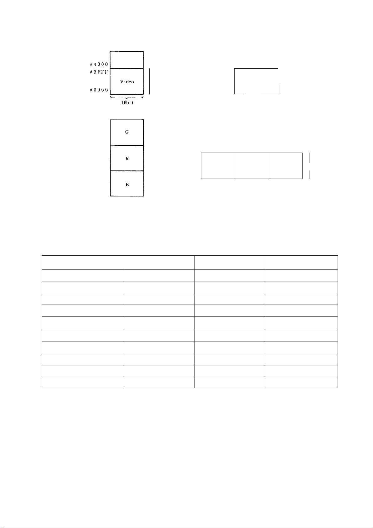
VIDEO
RAM
Memory mapper
Screen controller
CRT controller
Floppy disk controller
Parallel I/O port
Serial I/O port 8251
Counter
Clock
80 characters x 25 lines, 80 x 20, 40 x 25, or 40 x 20
Reverse, blink, line (horizontal, vertical)
2 channels (applicable CRT 640 x 400, 640 x 200, B/W or color)
256 bytes/sector, 16 sectors/track, 80 tracks/disk
Built-in interface for optional MFD
High class compatible with PC3200 BASIC, supplemented and graphic
control commands
Expanded RS232C, GPIB, and GPIO
BACKUP, INIT, COPY, DEBUG, KILLALL
8K Byte ROM
16K Bit SRAM X 4 chips
16K Bit SRAM X 1 chip
16KB'tSRAMx 1 chip
4K Bit SRAM X 2 chips
TH SP6102R001
SP6102C002
CSP-1
CSP 2
SP6102C003
*iPD7220
pPD765
8255
8253
pPD1990AC
HALT SW Speaker volume control
M 7 3500
I -
Page 3
MZ3500
1-2. MZ-1K01 (Keyboard) specification
Outline
Specification
Keyboard layout
Ш P In
MZ1K02 U.S. keyboard (ASCII)
MZ1K04 German keyboard
LSI, 1C
Keys (98)
Interfacing cables
Other
Cabinet
Keyboard controller
CMOSIC
Sculpture key
Alphanumeric keys
Mode switch
For data transfer with the CPU (serial) and power supply (transmission under 15,000 baud)
Use of coiled cable with 8-pin DIN plug
Repeat function
Indicators (4 LED's)
Molded Color Office gray
Size (W X H X L)
MZ1K03: U.K. keyboard (ISO).
MZ1K05: French keyboard
80C49 or 8749
4049 X 2,4514
Mechanical contact key, with life of 10,000,(Ю0 operations.
61 Ten key 15
1
Automatic repeat occurs 0.64 seconds after
continuous depression of the same key.
POWER, Alphanumeric keys
467 X 35 X 190
Function keys
Weight About 1.5kg (3.3 lb)
6 Definable keys 10
2 Two-key rollover
II in
1-3. MZ-1U02
Outline
Specifications
Refer to the page TIN "CIRCUIT DIAGRAM”
Expansion unit for the MZ-3500 series CPU, which can be attached to the rear side of the main unit.
Optional boards are plugged in to the expansion box.
The expansion box will accomodate up to four option boards.
Number of slots: 4 slots
Slot connector. 60-pin edge connector x 4
Area of the slot inserting option board: 140.5 x 140
Slot for option and slot number
Slot 4
о
MZ-1R06
(expansion RAM)
SFD l/F
Expansion RS232C
GPIO о
GPIB
(IEEE l/F)
Slotl
О о
Slot 2
Slots
о о
о о о
о
о о
о о о о
- 2-
Page 4
MZ3500
1-4. MZ-IR03
Outline
Specifications
Optional board used graphic display functions with the Model-3500 series CPU. It includes 32K6 of RAM.
It is inserted through the slot on the front panel of the PU.
The MZ-1U02 expansion box Is not required.
GDC Graphic controller MPD7220
LSI
' ——____VIDEO^^
Graphic functions
(Color must be
specified for each
dot, when the color
video unit is in use)
Software
BASIC graphic control statements
VIDEO RAM
Basic (buit-in)
Expansion
(optional)
640 X 200
green monitor
640 X 200
color monitor
640 X 400
green monitor
640 X 400
color monitor
16KDRAM X 16 (32KB)
16KORAM X 32 (64KB)
32KB
(basic)
640 X 200 dots
Two screens
_
-------
^
640 X 400 dots
One screen
^
--------------------SDISP
ODISP
CHANGE DISP Mode designation
GCOLOR
CLS
PSET Dot set
PRESET Dot reset
LINE
GTABLE
CIRCLE Circle creation
PAINT
GINPUT Input of graphic pattern
GDISP
GPRINT Output of graphic pattern on printer
GREAD
GENTER Input of pattern within the specified area
GCURSOR
GSCROL
SYMBOL Graphic symbol displaying
SCALE Scren scle-down designation
^
Screen designation for two video units.
Designation of output screen.
Graphic pattern designation
Cleared by the color specified.
Line creation
Table creation
Paint over
Display of graphic pattern
Read of coordinates
Graphic cursor position designation
Graphic screen scrolling
(maximum expansion)
96KB
640 X 200 dots
Six screens
640 X 200 dots
Two screens
640 X 400 dots
Three screens
640 X 400 dots
One screen
3 -
Page 5
MZ3500
1-6. MZ-1R06
Outline
Specifications
Optional board for memory expantion of the MZ-3500 sries CPU. with this option the main memory (RAM) can be expanded
up to a maximum of 256 KB.
This option plug into the expantion box in slot 1 or 3.
LSI
Memory and user
area
Basic
Expansion
Totai capacity of
the main CPU RAM
64KDRAM X 8 (64KBI
64KDRAM X 8 (128KB)
SYSTEM
BASIC
(RAM
BASE)
AREA
USER
AREA
Main CPU only
128 KB 192 KB
• 57 KB
80 KB
Use of MZ-1R06
-
128 KB
Using eight 64K RAM's
on the MZ-1R06
256 KB
-
208 KB
- 4 -
Page 6
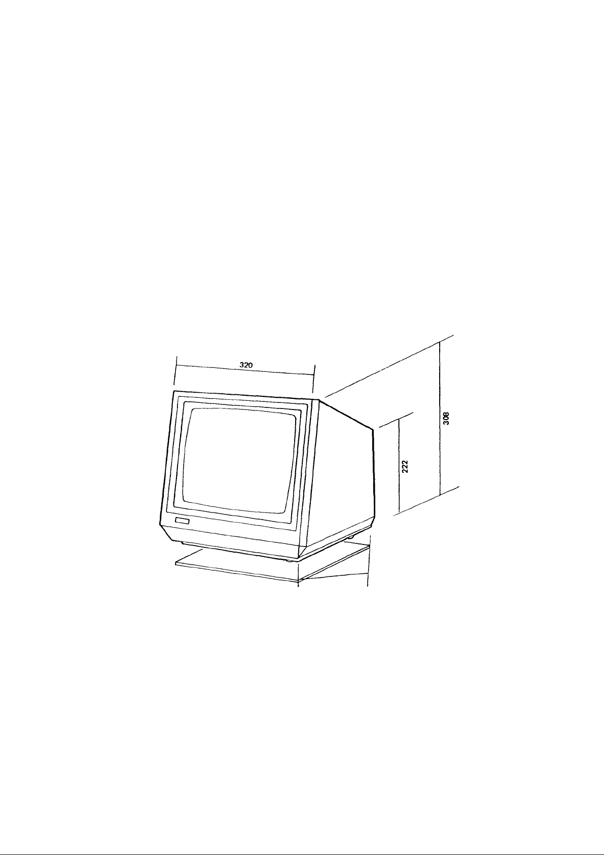
1-7. MZ-1D07
MZ3500
Outline
Specifications
High resolution MZ 3500 senes 12 green monitor
Video tube
Display capacity
Display size
Input signals
Power supply
Cabinet
Adjusting knobs
Accessories
Type
Fluorescent color P39 (green, long PERSISTANCE)
Total number of
display characters
220X145
Method
Horizontal 20 86kHz
29W power consumption
Molded
Size (W X H X L)
CPU connection cable and power cord and Tilt stand
Non glare green
2,000 characters
(80 characters x 25 lines)
Separate input, TTL level
Color
Vertical synchronization, contrast, brightness
Office gray
324x310x356
Size
Display capacity
Vertical
Weight
12”, 90 deflection
640 horizontal dots,
400 vertical lines
47 8 Hz
7.2 kg
(
- 5 -
Page 7
MZ3500
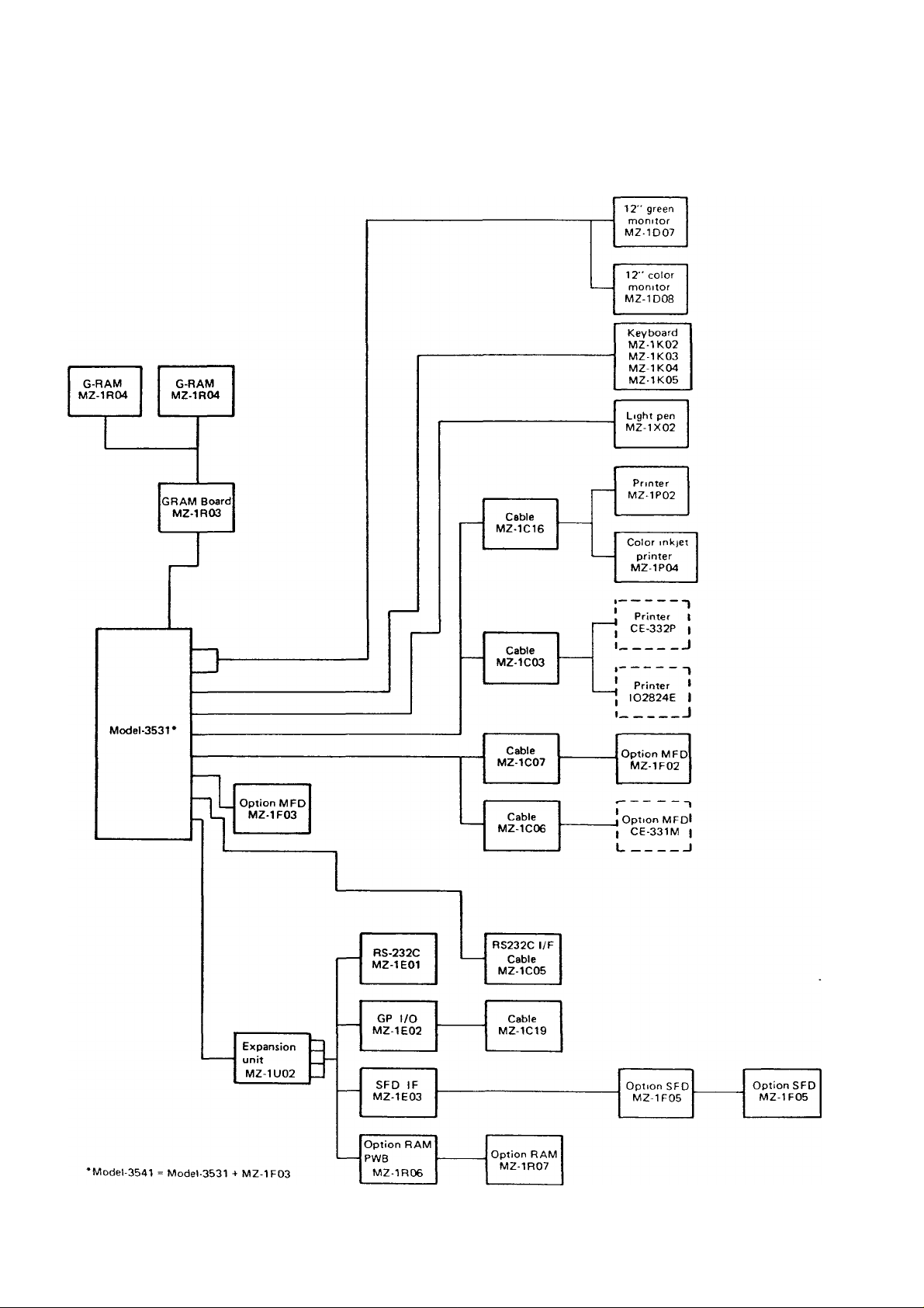
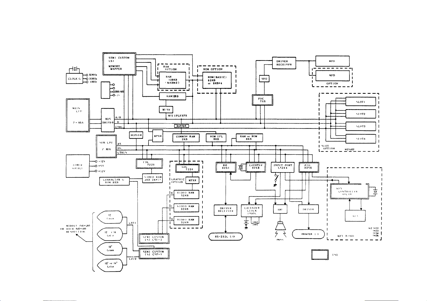
1-8. System configuration of Model 3500
6 -
Page 8
2. SOFTWARE (MEMORY) CONFIGURATION
MZ3500
Memory will be operated under four states of SDO ~ SD3,
depending on the hardware and software configurations.
In the paragraphs to follow, description will be made for
those four states.
MAIN CPU
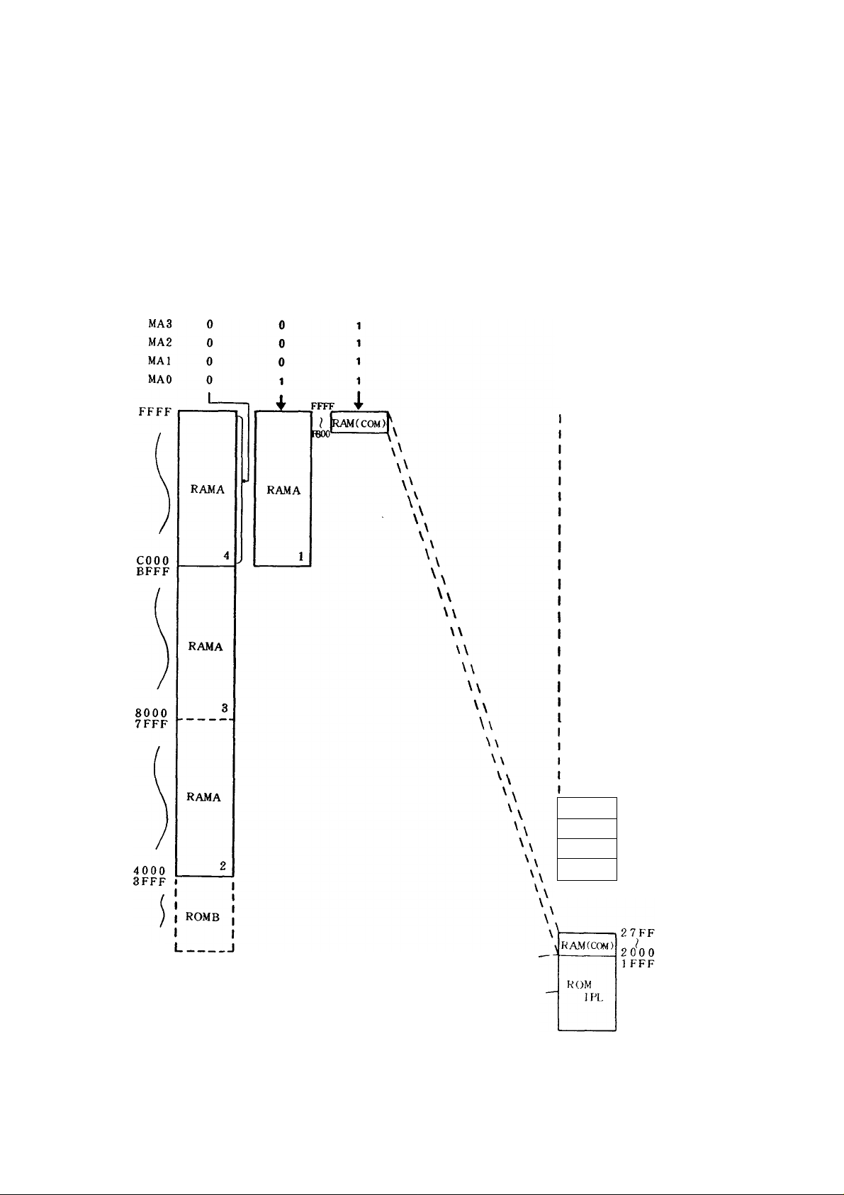
2-1. SDO (INITIALIZE STATE)
SDO can only exist immediately after power on, and the
system executes IPL under this condition and that the
system thus loaded will automatically assign memory area
for SDÌ, SD2. and SD3.
SUB CPU
MSI = 0 (L)
MSO = 0 (L)
2000
OFFF
0000
ROM
1 PL
ROM
(SPARE)
RAM
SD
RAM
SC
RAM
SB
RAM
SA
5F^FF
5800
57PF
5000
4FFF
im
4 000
0000
Page 9
MZ 3500
Operational description
(1) Upon reset after power on, the main CPU loads the
contents of the initial program loader (IPL) into RAM
starting at address 4000H, during which time reset is
applied to the sub-CPU.
TIMING OF RESET SIGNAL
The main CPU then terminates resetting the sub CPU
(2)
and starts the sub-CPU. At the same time, the ROM
IPL is assigned to the sub-CPU.
The main CPU then send the memory allocation (state)
(3)
to SDÌ, and starts to load DOS from the system floppy
disk.
Signal generated from the
CR network and power supply
Output signal from the mam CPU port
MAIN CPU
START
Memory Map Data:
1. ROM-B is tested to determine if ROM's are present.
2. The ROM-IPL functions under control of the main CPU
at first, but later it functions under the sub-CPU after
the IPL program has been loaded in RAM.
3. RAM-COM is shared by both the main CPU and the subCPU.
INITIALIZE FLOW „„t
a. Main CPU reset time
b. Main CPU IPL load time
4. Memories other than described above cannot be accessed
under the SDO state.
5. Bank select, MA0~MA3, is used within the address range
of COOOH-FFFFH.
''M* )S V 1 M/}
Page 10
MZS.'tOO
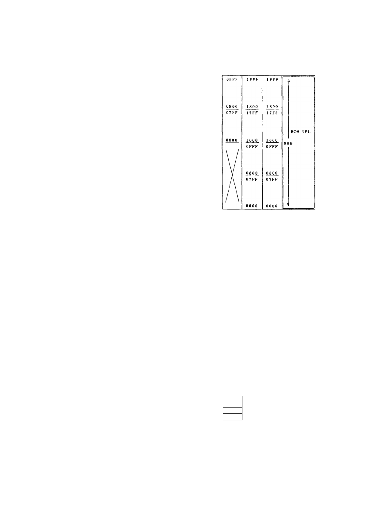
ROM-IPL
1. An 8KB ROM (2764 or mask ROM equivalent) is used
for the ROM-IPL.
2. When the system reset signal turns from low to high
state after power on, the main CPU starts to operate At
this stage, the ROM-IPL is addressed.
3. The CPU starts from address OOOOIROM address 10000)
4. The main CPU sets the sub-CPU reset signal from low to
high state as it goes out of its initial state via the memory
mapper and the sub-CPU starts to operate. At this point,
the ROM-IPL is addressed by the sub-CPU.
5. Address 0000 of the sub-CPU is ROM address (0000)
The memory area above ROM address (1000) cannot
be used by the sub-CPU because the mam CPU initial
program has been loaded there.
2-2. SDÌ (SYSTEM LOADING & CP/M)
SDÌ determines which operating system is in use. The
system is loaded in the CP/M (Control Program for Micro
processors) mode.
Mam CPU logical address (during IPL operation)
Logical address of the sub-CPU
ROM physical address
МЫ = 0( L)
WS0=l(Hj
FFFF
i
P800
F7FF
*
i. Л 0 n
-----
\
' \
\\
\ \
T
\ \
\ \
\ \
\ \
\ \
\ \
\ \
V \
\ \
RAM
RAM
RAM
\ \
RAM
\ \
\ \
\ \
\'
5FFF
sn
5800
57FF
SC
5000
4FFF
SB
4800
47FF
SA
Page 11
MZ3500
Operational description
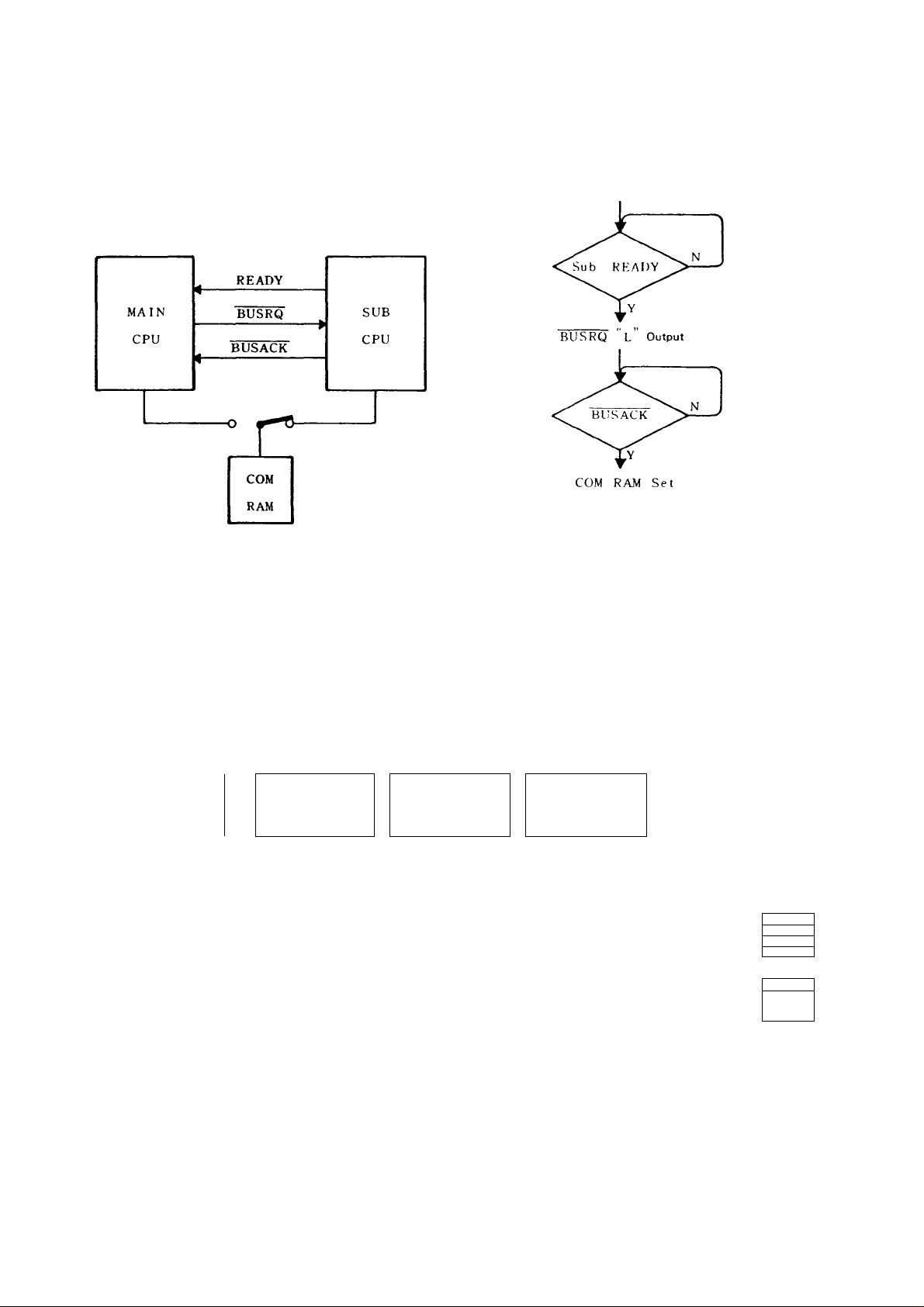
(1 ) As soon as the sub-CPU is started, it initializes the I/O
port and waits for program transfer (IOCS) from the
main CPU. This IOCS (Input Output Control System)
is the program resident at address 4000H-5FFFH.
(2) As the main CPU loads the information from sector
Communication between Main and SUB CPU
"1" of track "0" of the floppy disk, it loads the IOCS
and bootstrap routine to the sub-CPU.
(3) The bootstrap program is loaded next.
(4) The bootstrap program determines memory allocation.
I
BUSRQ H OUTPUT
"h
(ISOLATION OF COM RAM)
I
2.3. SD2 (ROM based BASIC)
SD2 is active when "SHARP BASIC" is executed via ROM.
RAM
BANK
SELECT
MA3 0 0
MA2 0 0
MAI 0 0
MAO 0 1
FFFF
KAMA
cooo
BFFF
4000
Ifff
2000
I FFF
4 1
KOMB
—I—1—1—
KAMb
1, 2 1 3|
0000
M02 0
MO] 0
MOO 0
MAIN CPU
---------1--------1--------\--------
A
ROM 2 ROMS
К AM L
1 1 2, 3, 4
--------
______
1--------1
KAM I*
i| г, 3| 4
MSI = u H )
Mso = 0 L;
--------1-------
SUB CPU
\
\\
\\
\\
\\
\\
\\
\\
\\
\\
RAM SD
\\
RAM
sc
RAM
SB
RAM
SA
RAM(aX)
ROM
J PL
1. Bank select. MA0~MA3, is effective for memory area COOOH-FFFFH.
2. Bank select. MOO—MA2, is effective for memory area 2000H-3FFFH
10 -
Page 12

2-4. SD3 (RAM based BASIC)
SD3 is active when "SHARP BASIC" is ececuted via RAM.
"SHARP BASIC" is loaded in RAM from the floppy disk.
MZ3500
MAIN CPU
МЛЗ 0
RAM
\ МЛ2 0
BANK
SELECT
I MAI 0
I MAO 0
I I г
RAM в
RAMA
lU 4L. 4U
2 I 3,
ROM!
cooo
BFFF
IFFF
0000
ROM («02 0 0 0 0 1
BANK (mo) 0 0 1 ' 1 0
SELECT /moo 0 10 I 0
1. Bank select, MA0-MA3, is effective for memory area COOOH-FFFFH.
2. Bank select, MO0-MO2, is effective for memory area 2000H-3FFFH.
0 0
1 1
0 0
0 i
----
RAMC
2j- -
1—
----1-----
KAMI)
MSI = 1 (H )
MSO = 1 ( H)
1
3,
ЕЩх
SUB CPU
\\
\'
\\
' \
RAM
sp
RAM
SC
_SA
ROMS
ROM BASE
OF THE
SUB CPU
RAM
EAM
\v
\ ЦМ(СШ)
ROM I PI
Operational description
The state of the system is determined by the bootstrap
program before the load of the system program.
Page 13
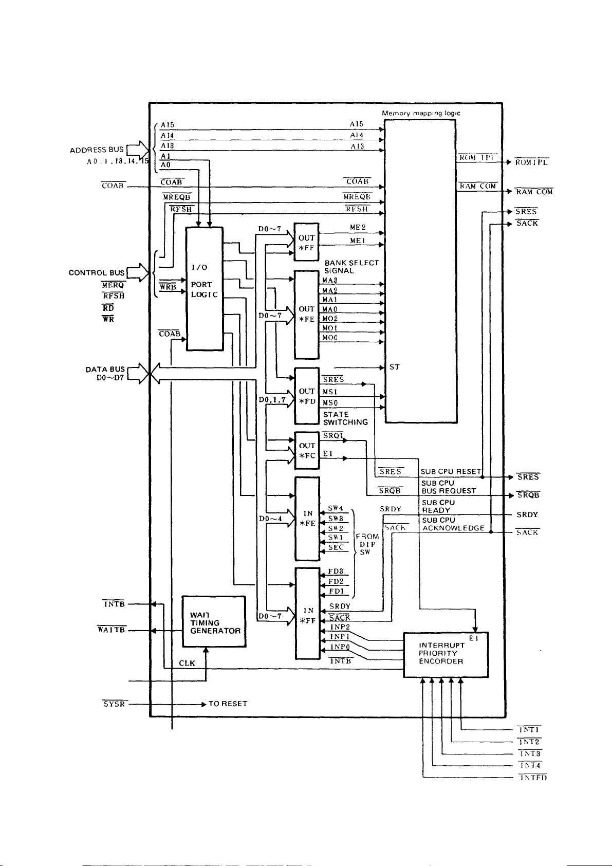
3-1. Block diagram
1) Relation between MMR (Main Memory Mapper) and
main memory.
3. CPU AND MEMORY
I
Page 14
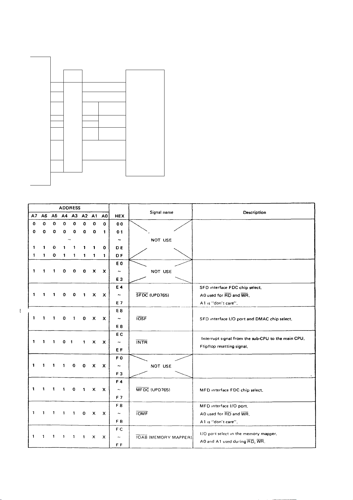
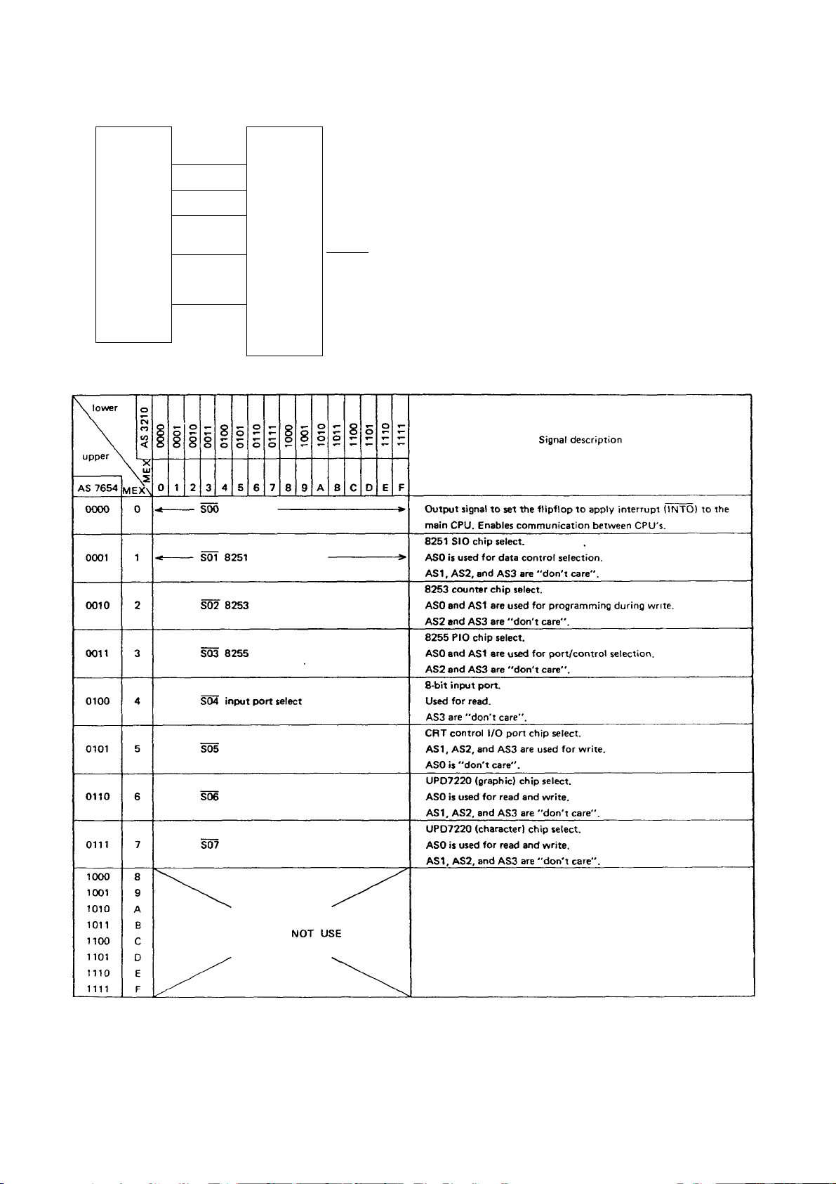
3-2. Main CPU and I/O port
M
A
1
N
C
P
u
A5
A6
A7
A2
AS
A4
lORQ
¥T
MZ3500
This paragraph discusses main CPU I/O
Connector port select and addressing.
I FC2 The address output from the main CPU
I is decoded in the 74LSI38 to create the
I select signal.
I Table below describes address map and
[ signal functions.
I
B
G2A
YO
Yi
Y2
Y3
SKDC
O lOSF
L© 'MTR !
Y4
u
G2B
G1
Y5
YG
MFUC
ijD lOMF^
I
I
74 LS138
Y7
lOABCMEMORY MAPPER)
- IT -
Page 15
MZ3500
3-3. Sub CPU and I/O port
AS6
ASS
SUB
CPU
AS7
3—
¥T
___
AS4 1
“c
Shown at the left is the circuit used by
Y7
4G
74LSI38
Y6
YS
Y4
Y3
Y2
Y1
YO
2.
B
G2A
G2B
6
G1
S07
S06
10 SOS
.11 S04
■ 12 S03
.15 S02
14 SOI
15 SOO
-►gdc-i
Graphic option
-►cSP-1 .CSP-2
-> Input port select (LS244)
-►8255-‘cT
-►8253-CS
-►8251-CS
MAINCPU-INT
the CPU to select the I/O ports The out
put address from the sub CPU is decoded
by the 74LS138to create the select signal.
Shown
below Is the address map and
select signals.
- 18 -
Page 16
3-4. Memory mapper (MMR) SP6102R-001
1) Block diagram
MZ3500
19 -
Page 17

MZ3500
2) Memory mapper (MMR) SP6102R-001 signal description
Pin No.
10
12
13
14
15
16
18
Polarity
Signal Name
ST
DO
07
A15
A13
A1 IN
SRES
SRQ
AR13
AR15
IN/OUT
IN
IN/OUT
IN
OUT
OUT
OUT
Function
Main CPU DRAM output buffer (LS244) switching strap.
Bidirectional main CPU data bus.
(Data bus 0 7)
Main CPU address bus.
Used in the memory mapping logic of the MMR for address output for the DRAM, ROM, and
shared RAM. (Address bus 13 ~ 15)
Main CPU address bus.
Used in the I/O port select logic of the MMR to assign device number
Sub-CPU bus request signal.
• After power on: Halts the sub-CPU.
• After write command (LDA-80H: OUT#FD) by the main CPU- Starts the sub-CPU.
This signal is issued after transfer of the main CPU program contained m the ROM-IPL.
(Sub CPU Reset)
Sub-CPU bus request signal.
• After power on: Resets bus request to sub-CPU.
• After write command (LDA-02H: OUT#FC) by the main CPU: Place bus request to the sub-CPU
This signal is issued to bus of the sub-CPU, after the main CPU writes to the shared RAM a command
parameter to the sub-CPU or reads the message status from the sub-CPU.
(Sob CPU Request)
Address signal to the main CPU dynamic RAM.
The main CPU addresssignals.A13-A 15, merged in the memory mapping logic circuit to produce
AR13-AR15. This is means by which the 4 basic and CP/M memory maps are made, along with MSI
and MSO.
19 R32 OUT
20
21
22 ROPB
23
26
27
30
31
lOAB
SRDY
ROAB
RODB
RSAB
RSDB
SACK
OUT
OUT
•R32B (alternate choice with the 32KB mask ROM chip select signal).
OUT
IN
IN
IN
BASIC interpreter 32KB mask ROM chip select signal.
Valid when SD2 is active (Sharp ROM based BASIC). Command ILDA 02H OUT 3F D)
(ROM 32K select)
Internal MMR I/O port select logic signal.
Goes low by the command IN/OUT #FC-#FF.
(Input/Output Address)
Input of ready signal from the sub-CPU.
(Sub CPU Ready)
Chip select signal issued from the main CPU to the 8KB mask ROM.
Valid with SDO active (initialize state).
(ROM ipl)
Chip select signal for four chip BASIC interpreter 8KB EPROM (A. B, C, D).
Valid with SD2 active (Sharp ROM based BASIC).
(ROM A~D Buffer)
Row address select signal for the main CPU dynamic RAM (block A-block D).
RAS (ROW ADDRESS SELECT; LINE ADDRESS SELECT) SIGNAL
(Row address Select)
Input of bus acknowledge signal from the sub-CPU.
When the mam CPU must write a command in the shared RAM a bus request is issued first, then the
command is written in the shared RAM after acknowledgement from the sub-CPU
I At the end of the command cycle bus request is released and the sub CPU executes the command
20-
Page 18
M7-3S00
Polarity
Pin No.
Signai Name
32
33
34
35 RCMB
36
37
38
39
40 MRQB IN
RF1B
RF2B
WATB
ITFB IN
ITOB
IT1B
ÏT2B
IN/OUT Function
OUT
OUT
OUT
OUT
IN
IN
Mam CPU 128KB dynamic RAM output buffer (LS244) output enable signal.
(RAM buffer 1)
Signal identical to R F1 B For option RAM
(RAM buffer 2)
Wait signal to the mam CPU
(One wait cycle is applied during the memory fetch cycle of the main CPU. It consists of one dock
period) (WAIT)
Chip select signat issued from the main CPU to select the RAM shared by the main CPU and
the sub-CPU
(RAM Common)
Interrupt input from the UPD765 FDC (Floppy Disk Controller). |
(Interrupt from Floppy)
Interrupt input from the sub-CPU.
(Interrupt from No. 0)
Interrupt input from slot 1 or 2.
(Interrupt from No. 1, 2)
Memory request signal from the main CPU.
(Memory Request)
41
42
43
44
45 GND
46 Vcc
47
48
49
50
61
52
53
IT3B
ÏT«
SEC IN
SW1
SW2
AO
RFSH
SW3
SW4
GND IN
IN
IN
IN
IN
IN
IN
IN
IN
Write signal from the mam CPU.
(Write)
Interrupt input from slot 3 or 4.
(Interrupt from No. 3, 4)
Input from the FDD (Floppy Disk Drive) assignment dip switch (A), No. 1.
*See the dip switch description, provided separately.
(Section)
Ground
5V supply
Input from the svstem assignment dip switch.
*See The dip swtch description, provided separately.
Mam CPU address bus
Used in the I/O port select logic in the MMR to designate device number.
Refresh signal from the main CPU,
(Refresh)
Input from the system assignment dip switch.
'See the dip switch description, provided separately.
Ground
54
55
56
FD1
Vcc
FD2
IN
IN 5V supply.
IN
Input from the system assignment dip switch.
'See the dip switch description, provided separately.
Input from the FDD assignment dip switch (A), No. 2.
'See the dip swi*ch description, provided separately.
- 21 -
Page 19

M/.3500
Pm No
Polarity
Signal Name
57 SYSR IN
58
59
FD3
COAB IN
60 R01B
61
62
63
64
65
66
GND IN
Vcc IN
R02B
R03B
RDB
CLK
IN/OUT
IN
OUT
OUT
IN
Function
System reset signal.
Used to reset I/O port in the MMR.
(System Reset)
Input from the sytem assignment dip switch.
•$ee the dip switch description, provided separately.
Shared RAM select signal.
Address of the shared RAM is i?F800-#FFFF for the main CPU
(Common RAM Address)
Select signal for 8KB area allocated to slot 1.
Valid when SD2 is active (ROM based BASIC) and SD3 (RAM based BASIC)
(ROM 1)
Ground
5V supply
Select signal for 8KB area allocated to slot 2 or 3.
Valid when SD2 is active (ROM based BASIC) and SD3 (RAM based BASIC).
(ROM2, 3)
Read signal from the main CPU.
(Read)
EAIT signal generation clocit.
(Clock)
67 R04B OUT
68
69
MPX
GND IN
OUT
70 CASB OUT
71 GND
72
INTB
IN Ground
OUT
73
Select signal for 8KB area allocated to slot 4.
Valid when SD2 or SD3 (RAM based BASIC) are active.
(ROM 4)
RAS/CAS address switching signal for the main CPU DRAM.
High: Row address Low: Column address
(Multiplex)
Ground
CAS (Column Address) signal for the main CPU 64K DRAM.
•Refresh for the RAM only.
(Column Address Select Buffer)
Interrupt signal to the main CPU.
(Interrupt)
Not used
Page 20
MAIN CPU
I/O PORT IN MEMORY MAPPER
ADDKKSS
-\7 A6 A5 A4 A3 A2 Al AO
111110 0
1111110 1
11111110
11111111
HEX
EC
El)
FE
FF
DHUS
DI
DO
D7
DO
1)7
U6
D5
D4
D2
D1
DO
D4
D3
D2
D1
DO
D7
D6
D5
1)4
D3
D2
U1
DO
D7
D6
1 ()
OUT
OUT
IN
IN
OUT
SKUH
I I
SKI s
MSI
MSO
MA2
MAI
MAO
M02
MOl
MOO
S\\4
S\)3
S'\2
Stt 1
SEC
FD3
FD2
EDI
SKDY
SACK
1 NP2
INPl
1 NPO
MF2
ME 1
SRQ Bus request from the main CPU to the sub-CPU
Sub-CPU reset signal
Memory system define
Bank select signal to memory area of COOO-FFFF.
Bank select signal to memory area of 2000-3FFF.
System assign switch
FD assign
t. ^------------------------------------------
TÌ1 Sub-CPU READY signal
V Sub-CPU acknowledge signal
Interrupt status
#1
M/3S00
(SW8)
1. All output signals are reset to low level upon power on,
' except for SRBQ that goes high.
2. Noted with a star mark "A" are input/output signals, and
rest of others are processed in the LSI.
#1 I/O port output of MEI and ME2 uses the memory at
the addresses.
( ME2-^8000~ BFFF
1 MEI ^4000 ~7FFF
When MEI and ME2 are in high state, RSAB (RASA) is
inhibited during memory addresses in RAM-A that
correspond to overlayed addresses for ME! and ME2
This is not true during SDÌ mode.
_____
- 23 -
‘ VK IN MEMCKT MM I Mf
'
, X 1
1 " i "
Wait timing generator
WAIT IS issued once per main CPU fetch cycle.
Its outui IS tri state
MFH noh
1 TsTTiT
1 H
f " ÌLtT“
M I TO ENCODMf
IMP 112h
IMI
IN=Tt INF?
'I
1
M 1 X
H
” -J
, " 1 '
II
H
X X
X X
X X
H M
H H
FkoM SI Ml
I h <• 11
ii3h 1T4H
JNT3
X X
>H
<*nriT M(t»M FNCODFK
IM 2
INT4 Tvf
1 1 L
X X
X
X
L H L
1
1
L
H
X X tl
H L
H H
■ ^ ■
—
IMH
IM «
L
H
L
1
X
TO MAIN Cl I
Page 21
MZ3500
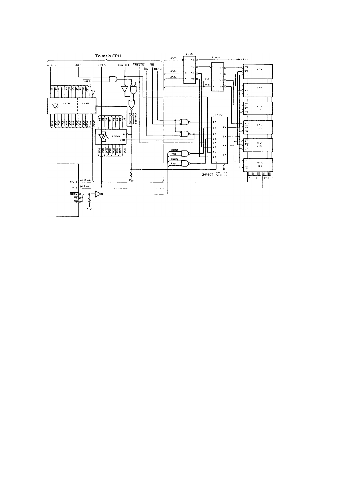
3-5. Memory (ROMIPL, RAMCOM, S RAM) select circuit
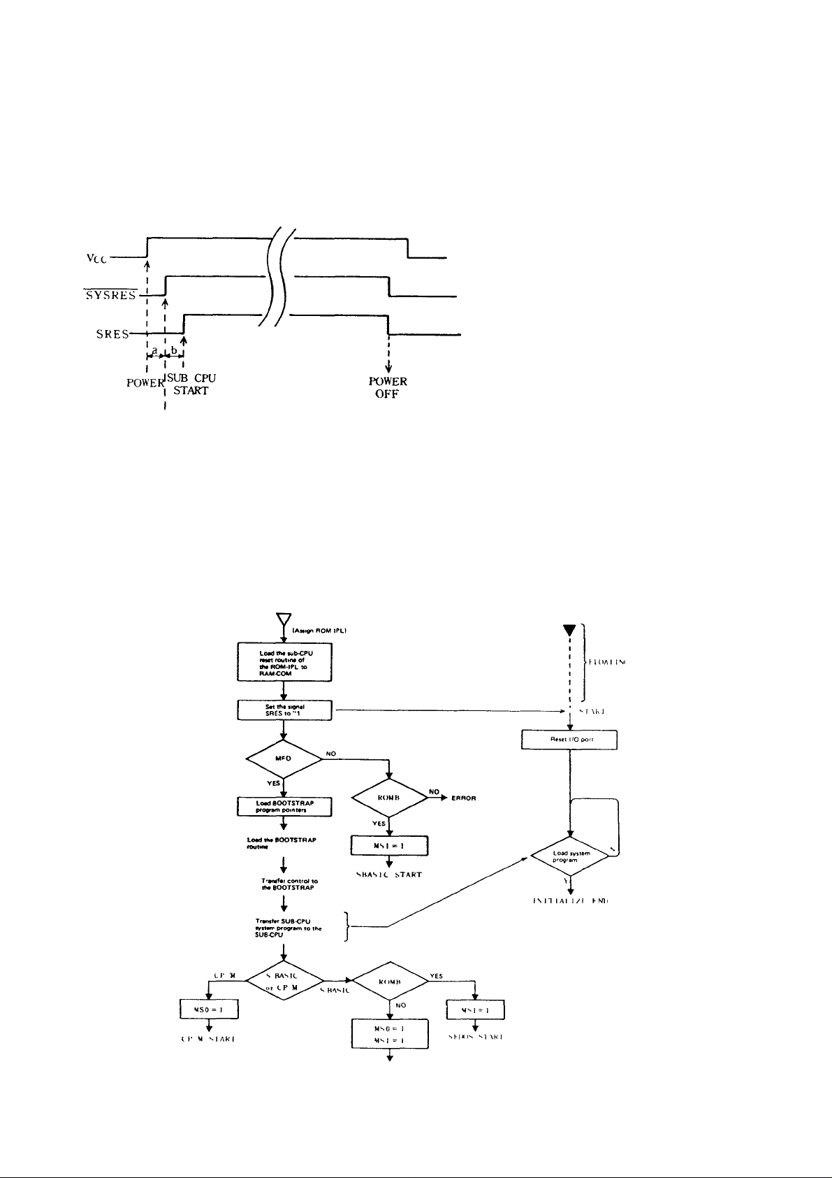
1) ROM-IPL select by the main CPU
As ROM IPL turns to low level after power on address
bus buffers {LS244, LS367) and data bus buffer
(LS245) are enabled. S of the data selector 1C (LS157)
is set to a low level to enable input 1A-4A. The 3Y and
2Y outputs of the LSI 57 then go low so that CE and OE
of the ROM-IPL are from main CPU. The contents of
the IPL-ROM are then read by the main CPU. Because
the input pin (ff16) of the address buffer (LS367) is
connected to Vcc, IPL for the main CPU will be at
address 1000 of the IPL-ROM. Switch SW2BA is the
operation test dip switch which should be ON at all
times.
2) RAM-COM select by the main CPU
When RAM COM is low, SRES high, and SACK low, the
select input S of the selector 1C (LSI 57) is in low state
so that input 1A-4A becomes effective. That is, the out
put 4Y is low and either 1Y (WE) or 2Y (OE) becomes
low level, so as to enable to read or write RAM-COM.
3) ROM-IPL select by sub-CPU
Normally, the select signal S of the selector is pulled up
to Vcc level that inputs 1B-4B are enabled by sub CPU.
If A13 thru A15 were to be at low level, the output YO
of the LSI39 becomes low level so that the output 3Y
of the LS147 or CE of the ROM-IPL should be at low
level. Should SRD, SMRO be at low lebel as well, the
output 2Y of the LSI57 or OE of the ROM-IPL turnde
to low lebel to read the ROM-IPL. Though the sub-CPU
can access an address range of 0000 to 1FFF theoretical
ly, it would be from 0000 to OFFF, actually.
4) RAM-COM select by sub-CPU
Y1 of the LS139 changes to low level when AS13 is high
and AS14 and AS15 are low. In other words, the input
4B of the LSI 57 is at low level which brings the output
Y4 to low level, so that CS of the RAM-COM chip select
signal should become effective.
If SMRO, SRD or SMRO, SWR is in low level at this
point, it enables read (OE) or write (WE). Address range,
however, is 2000 to 3FFF
5) RAM (SA, SB, SC, SD) select by sub-CPU
SMRO, S^ (OE) or SMRO, SWR (WE) is at low level
to select the sub-CPU dedicated RAM, SA-SD. Tne
following chip select signal, then becomes valid under
these conditions:
RAMSA .. AS11, AS12, AS13, AS14, AS15
(address 4000-47FF)
RAMSB .. AS11, AST2, ASi^, AS14, AS15
(address 4800-fFFF)
RAMSC .. AS11, AS12, AS13, AS14, AS15
(address 5000-57FF)
RAMSD .. ASH, AS12, AST3, ASK, AS15
(address 5800-5FFF)
- 24 -
Page 22

4-1. Specification
y-/ rr-,^
4. CRT DISPLAY
Display memory
Character display
Graphic display
(option)
Ust of fiigh resduiion CRT
3KB (characu>-$l
96KB, max (graphtc i
Screen structure
Programmable
Character
structure
Attributes
Colors 8 colors, programmable for each character
80 chrs X 25 lines, 80 chrs x 20 lines
40 chrs X 25 lines, 40 chrs x 20 lines
8x16 dots
With lower case descenders
255 characters
Alphanumerics and 69 symbols
26 small characters
97 graphic patterns
Revers, vertical line, bhnk, horizontal line
Programmable for each character
Option
32KB type 640 X 400 dots, B/W (one frame)
Color designation for each character
96KB type
640 X 400 dots. B/W (three frames)
Color designation possible for each character
Color (one f rante)
Use of medium resolution i,RT
8x8 dots
Blink, revers
Programmable for each character.
640 X 200 dots, B/W (Two frames)
Color designation possible for each character
640 X 200 dots, B/W (six frames)
Color designation possible for each character
Color (Two frame)
Screen merge
Merge of chracters and graphics
Merge any graphic screen (1 to 3 frames)
Merge a character screen with a graphic screen
Background color Choice of 8 colors
Control of two independent screens Possible to d bpiav on separate two screens origma' graphic scieen and character screen
Separate graphic screens can be merged into one
Possible to affix attributes (CRT2 only)
Selection of character/non-character screen display
Control channel number
Light pen input (option)
Incorporation of two independent video outut channels
Scans coordinates and character code
23 •
Page 23
Summary of video display specification
Table 1
High resolution CRT (640 x 400 dots mode)
Type of monitor
Characters
Function
Elements
Character structure 5x14 5x14
Screen structure
(Characters x lines)
Basic
Color
designation
Small letter descenders 0
Line creation
Display memory
Frames
overlay
Option 1 (48KB)
Option II (96KB)
Basic
Option 1 (48KB1
Option II (96KB)
Basic
Option 1 (48KB)
Option II (96 K B}
ASCd
8 X 20
80 X 25 mode 80 X 25
80 X 20 mode
40 X 25 mode
40 X 20 mode
One character screen against
one gra'C'hic screen
One character screen Tgambi
three graphic screens
Green monitor
Graphics (option) Characters Graphics (option) Characters
8x16
640 X 400 dot
0
3KB
1 frame
t 1 frame
t
Not possible
B/W
32KB 3KB 32KB (1), 96KB(ll)
No frame
3 frames
ASCII
8 X 16
8 X 20
80 X 20
40 X 25
40 X 20 40 X 20 40 X 20
By character By character
1 By character
t
O
X
1 frame
f 1 frame
t 1 frame
One character screen against
one graphic screen
One B/W character screen agamst
three graphic screens
One color character screen against
one graphic screen
Color monitor
-
Color
640 X 400
By dot
No frame
Medium resolution CRT (640 x 200 dots mode)
Green monitor
Graphics (option) Characters
ASCII
8x8
8x10
5x7 5x7
80 X 25 80 X 25
80 X 20
40 X 25
X X
X X
3KB 16KB 3KB
1 frame (1 page)
t
t
*- -
One character screen against
three graphic screens
’
B/W
640 X 200
No frame 1 frame (1 page) No frame
3 frames
6 frames
Color monitor
Graphics (option)
ASCII
8x8
8x10
80 X 20
40 X 25
t
1
t
t
One 8/W character screen agamst
three graphic screens
One color character screen agamst
one graphic screen
640 X 200
1 frame
2 frames
I
Color
By dot
t
48KB
NOTE Graphics opi'on
Page 24
1) Character display
1.1. Screen structure
M7 3500
CRT used , (640 x 400 dot)
, High resolution CRT
Character |! INewlfV = 47 3Hz
80 X 25 lines
ASCIL
80 X 25 lines
40 X 25 lines
40 X 20 lines
|| fH = 20 9KHz
Medium resolution CRT
(640 X 200 dot)
fH = 15 7KHz
fV = 60Hz
-
Dip switch in the main unit is used to select assignment of
high resolution/medium resolution CRT.
Display mode must be chosen by programming.
1-2. Character structure and picture elements
640 X 200
Structure
8x8
8x10
T
Small tetter descenders
and line creating
functions are not
available.
5x7
8x8
ASCII
Graphic
symbol
640 X 400
Elements
8x16
8 X 20
1
Small letter descenders
and line creating
functions are available.
Structure Elements
5x14
8x16
NOTE: In the case of 8 x 8 and 8x16 picture elements,
vertically adjoining graphic symbols will joint
together in the 25-line mode.
As for character structure of 6 x 14, 7 x 14, 6x7,
or 7 X 7, decision must be given on an actual dot
pattern.
2) Graphic display (option)
(High resolution CRT) (Medium resolution CRT)
640 dot 640 dot
200 dot
Dot pitch
Horizontal vertical
1 1
400 dot
Dot pitch
Horizontal vertical = 1 ; 2
W While
4) Attribute
B/W
ATI Vertical line
Horizontal line
AT2
AT3
AT4
Reverse
Blink
Color
Blink
Designated for each chaia-
cter.
B
R
Line and character r, .uV
G
exist in the same element
(Line may also be dis
played on the 80 charac
ters X 25 lines screen.)
5) Screen overlay
It will be possible to have an overlaid screen that consists
of one character (screen and a maximum of three
graphic screens. (For detail of overlay screen, refer to
Table 1.)
In the color mode, if there are two colors in the same
screen and other designated for a dot on the graphic
screen element — the one designated for a character on
the character — both colors will be merged altogether
to produce image.
(Red)
@ Dot color designated by
character attribute
(Blue)
O Dot color designated by
graphic dot.
(Violet)
^ Dot composed of more than
two color lD .i-jmtior.:.
3) Color designation
Eight colors are usable (white, yellow, cyan, green,
violet, red, blue, black)
Color designation
640 X 400 dot
ASCII By character
Graphics
48K byte By character By dot
96 K by te
By dot By dot
Background color
8 colors for designation
640 X 200 dot
By character
•¿1 -
Page 25
MZ 3500
6) Screen overlay and displaying on two independent
CRT’s
As there are two video output channels it will be pos
sible to display two independent screens on separate
video display unit Overlay is possible on either of
screens (See preceding item 5) ) The following bit
selection is needed for screen overlay
CSP 1
Address Data
AS
Hex
3
50 0
51 0 0
52
0
53
0
54
0
55 0
(5D)
AS
AS AS DS DS PS S gnal name
2 1
0 0
0
0 1
1
1
0 2 0
0
1
0
1
1
0 1
1
1 1
1
0
0 1 COLOR Color mode
1
1
0
1
1 ECHI
1
1
1
1 BGC R 1 Choice of background color display
1
1
1
Internal
of CSP
Choice of outputting the character screen on CRT1 0 No 1 Yes
ECH2
EAT2
SRI Displays on CRTI the blue elements contained m the VRAM
SR2
SR3
SR4
SR5
SR6 Displays on CRT2 the green elements contained in the VRAM
BGC B
BGC G
BODER Border color mode in effect
08/16 Defines the data size for the graphic RAM (0 8 bits, 1 16 bits)
40/80 Defines display digits for the character screen
Cho ce of outputting the character screen on CRT2 0 No 1 Yes
Choice of whether attribute or cursor be put on the frame that displayed
on CRT2 (0 No 1 Yes)
Displays on CRTI the red elements contained in the VRAM
Displays on CRTI the green elements contained in the VRAM
Displays on CRT2 the blue elements contained in the VRAM
Displays on CRT2 the red elements contained in the VRAM
<0 40 digits 1 80 digits)
Function
56 0
57 0
5D 1 1 0 1
CSP 2
NOTE Both CRT1 and CRT2 must be high resolution CRT's (640 x 400) or medium resolution CRT’s fC40 y 'tftt))
Output to each CRT may be possible in the following
CRT I
CH ( AT )
GF( AT)
CH AI )+(> ! ^ AT )
1
1
1 1
0 1
1
1 V RAM1
1
1
1
1
1
RA-400
V RAM2
1
25/20
1 08/16
40/80
Connection of a 400 raster CRT
Connection of the 96K bytes VRAM
Connection of graphio GDC
25 lines/20 lines switching (0 25 lines, 1 20 lines)
Defines data size for the graphic RAM (0 8 bits 1 16 bits)
Defines display digits for the character screen
(0 40 digits, 1 80 digits)
Output to each CRT may be possible in the following combination .
CRT 2
CH(AT)
(.F AT)
CH(Arj+C.i Al
CH ASCII
GF Graphic screen, including overlay of two graphics
(AT) Attached with attribute
CH
(.F
CH+(,I
screens
Page 26
7) ASCII CG
Uses an 8KB MROM contains two patterns'
640 X 400 dots (8x16 dots) and 640 x 200 dots (8x8
dots)
#0FFF
8x8 dot pattern
(2K bvte)
8x8 dot pattern
#0 000
(2K byte)
#1FFF
For Model 3200 senes
Without lower-case,
letter descenders
MZ3500
With 8x8 dot format
two kinds of patterns coexist
Refer to ROM address and data
code on separate information
8x16 dot pattern
(4K byte)
With lower-case,
letter (h i j) descenders
#1000
* Address and pattern in picture element
(Example of 5 x 12 dots pattern for 1 x 16 elements)
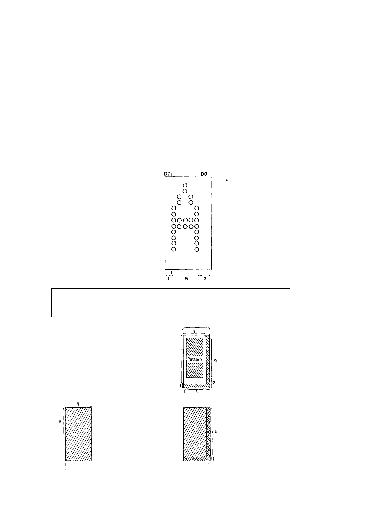
8) Element structure, character structure, and line
Element structure, character structure, and line
640 X 200 dot
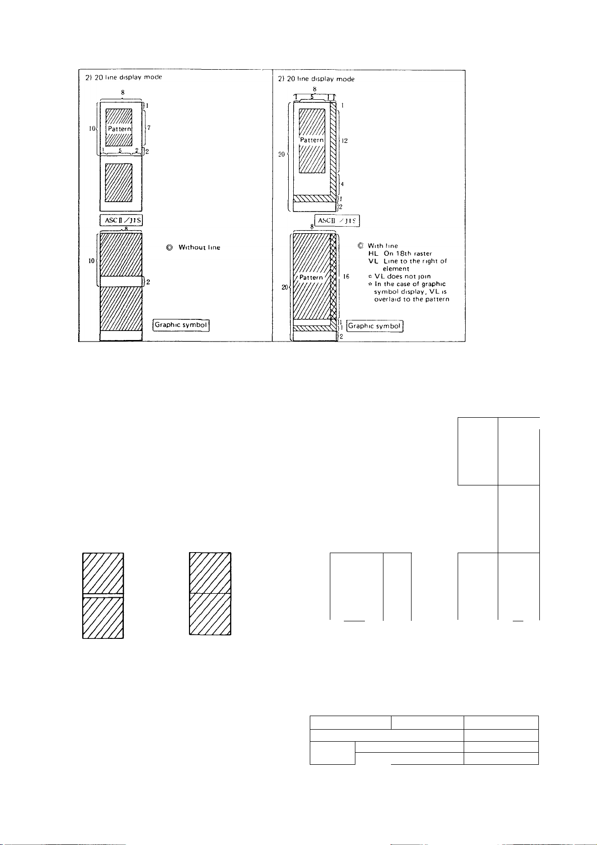
1) 25 line display mode
8
12
1) 25 line display mode
Model 3500
(Address) (Data)
#1000
#00
#1001 10
#1002 10
#1003 28
#1004
#1005
#1006
#1007
28
44
44
7C
#1008 7C
#1009
44
#100A 44
#1006
44
#100C 44
#100D
#100E
.#100F
00
00
00
/ — Character pattern area
\— Line area
X— Area where pattern and line are overload
640 X 400 dot
8
Pattern
iC
Pattern
1 5 2
ASCD/JIS
Graphic symbol^
Without line
15
ASCQ/J IS
[Graphic symbol]
29 -
’ With line
HL On 16th line
VL Line oi the right of
element
In the case of graphic
symbol display
* Both HL and VL are
overlaid to the pattern
Page 27
MZ3500
9) Cursor
Sharp of the cursor: Same as seen in Model 3200
Reverse and blink)
10) Light pen input
incorporates the light pen input connector and its inter
face. The light p>en, however, is an option.
Accuracy: By each character
Function: Coordinates/character code
11) Difference in specification with that of Model 3200
(1) There are two modes for the Model 3200; normal
mode (6x9 elements) and graphic mode (6x8 ele
ments). In the normal mode of 25-line displaying of
the PC-3200, vertically adjacent graphic symbols do
not joint. But, they will joint with the Model 3500.
Model-3200 Model 3500
(2) No line will be displayed for the medium resolution
CRT (640x200 dot).
It is possible to display line on the high resolution
CRT, compatible to line the utilizing program of
the Model 3200
4-2. Video RAM
1) Structure of VRAM
GDCl (for character)
GDC2 (for graphic)
#BFFF
16Kbit
x8
(G)
17FFF
1
1
1
Attribute
1
#07FF
2Kbit > 8
2Kbit
( S-RA.M )
(ASCI L
(. s-
R.AM)
#0000
DO-
VRAM capacity Graphic option 1: 48KB
Basic 3KB (including altibutes) Graphic option 2 96KB
Bit structure of VRAM
Character VRAM |
Graphic
V RAM
-D7 1)8—011
__
___CRT
48 KB 1 16 bit / word
96 KB 1 16 bit / word
#3FFF
x4
#0000
Solid line 48KB option
Broken line. To be added to comprise
640 X 400 dot
8 bit / word 8 bit / word
1
\
1
(D-RAM)
16Kb, t
x8
( B)
DO
------
D7 D8-
the 96KB option.
640 X 200 dcn
8 bit / word
16 bit / wo'd
-----------
_
________
I6Kbit
(R)
n
J
x8
-D15
- 30 -
Page 28
2) Read/write from Z 80 to VRAM
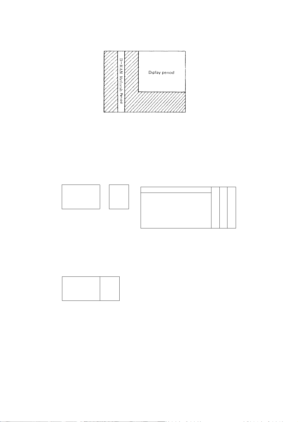
(1) Timing period for display and
V-RAM Read/write.
M7 3500
^>-'7 Range wh°ra RDC can draw.
Fly back perfod
H • SYNC-
J~L
BLNK-
(2) Timing that the Z-80 can read/write VRAM
The Z-80 can read/write VRAM when GDC FIFO
buffer is either empty or Full, and can be accessed by
3) Structure of character VRAM
(1) When read/write from GDC
#07FF
2KX8
ASC 1 I
#0000
DO
8bi t
(A)
-D7 D8
2KX4
Attribute
4 b I t
----------
(B)
► Dll
T_
refreshing during the display period. Number of
characters that can be read/write within one raster in
any mode.
(A)
-----------------------------------------------1--1
1
-
--------
----
----------------
ASC I K8bit) (
( I2bil ) )
no D1 D2 D3 D4 D5 D6 D7|d0
(B)
DI D2
- —
D3
■ Blink
Reverse (G)
. Vertical line IR)
. Horizontal line (B)
(2) During display
#07FF
#0000
2KX8
12bi t
(A)
(B)
2KX4
31
Page 29
MZ3500
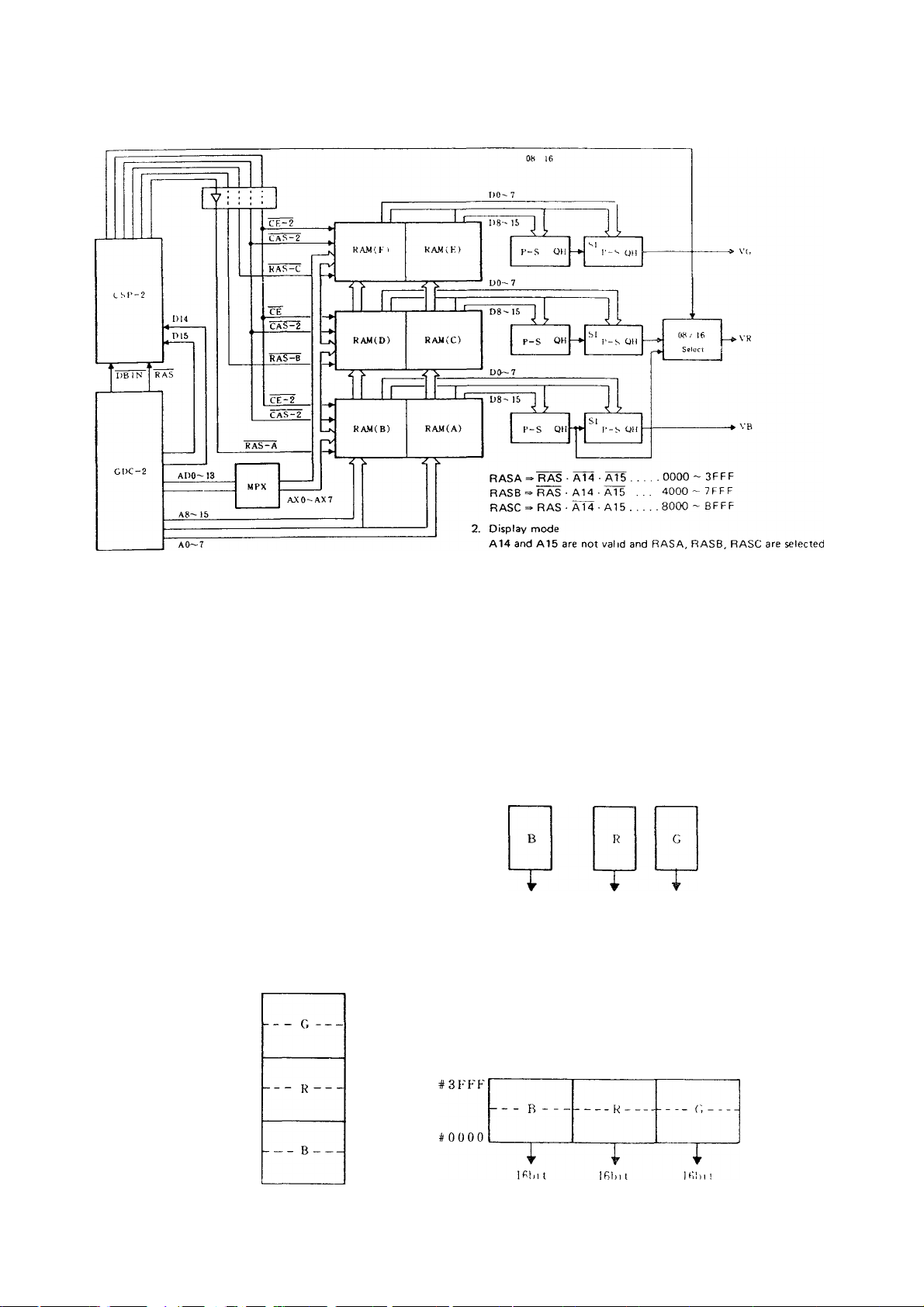
4) Graphic VRAM memory (MZIR03)
• Block Diagram
1. read/wnte Mode
The select signal RASA, RASB and RASC are generate from
R AS, A14 and A15 which is signal of GDC-2.
The address »5 allocated to each area selected by above signal.
Read/write by Z-80 via the GDC
(1) 640 X 200 dots display mode
Low High
byte byte
Option I #BFFF
(48K byte)
8bit structure
+ 8000
I I
I t
#4000
I
I
16K
#0000
8b it 8bit
Option II # BFFF
(96K byte)
16bit structure
together. By the DBiN signal from GDC-2, 08/16 signal is gener
ated by CSP-2.
The signal of 08/16 select, after P-5 conversion for RAMA,
RAMB output signal then output to VB by serial signal, or sprit
the signal to VB and VR.
(08/16 select: 08 for 200 rasters, 16 for 400 rasters}
During displaying
B/W: 3 frames
Color: 1 frame
#3FFF
16K
#0000
8bit
8bu
B/W: 6 frames
Color: 2 frames
# 8000
# 4 0 0 0
+ 00 00
I6bit
I6K
16K
- 32 ■
Page 30
MZ3500
(2) 640 X 400 dots display mode
Option i
{48K byte)
Option 11
(96K byte)
16 bits structure
#8000
#4 000
#0000
16bit
A #3FFF
16K
V #0000
16K
#3FFF
#0000
B
i
16bi t
B/W: 1 frame
Color: 1 frame
Video 1
_____
T
16bit
B/W: 3 frames
Color: 1 frame
K G
i
I6bit
1
1 tr
Color can be
designated for
each character
J6K
i
16bit
16K
A
5) Synchronize signal timing
(1) For 640 X 200 dots display mode
fH = 15.87kHz
fV = 60 Hz
Dot clock (00)
2XCCLK
Horizontal display time
HFP
HS
HBP
Vertical display time
VFP
vs
VBP
Total rasters: 261 rasters
Display raster: 200 rasters
GDC-1 (80 digits)
Character display (40 digits)
(16MHz)
( 8MHz)
(4MHz)
<2MHz>
40ms
7ms
6/JS
10ms (20 Chr.)
12,6ms
1.2ms
1 ms
1.8ms
—1
n
8 bits
16MHz
4MHz
-
^ (14 Chr.)
(1? Chr )
(tREF-0.8ms)
-
-
-
-
GDC-2
X : Y - 1 : 2
graphic)
16 bits
16MHz
2MHz
-
10ms
5jus
(tREF-1.6ms)
8iis
-
-
-
-
33 ■
ii
_TL
2rn- h
Page 31

Mzasoo
(2) 640 X 400 bits display mode
fH = 20.92 kHz
fV = 47.3 Hz
O
X : Y : 1 : 1
--------
Dot clock (OD)
2XCCLK
Horizontal display time 32 55^s 80 Chr. /40 Chr.
HFP
HS
HBP
Vertical display time
VFP
VP
VBP
Total rasters; 441 rasters
Display rasters 400 rasters
(3) CRT synchronizing signal specification (400 raster
CRT)
1. Horizontal synchronization frequency (fH): 20.92kHz
2. Vercial synchronization frequency (fV): 47,3Hz
3. Total rasters: 441 rasters
4. Rasters used: 400 rasters
5. Display dots; 640 x 400 dots
6. Dot clock: (19.66MHz)
7. Timing
( Neijanve)
V ideo
( Pom t ive
IT
GDC-1 (80 digits)
Character display (40 digits)
(19 66MHz)
(9 83 MHz)
(4.9152MHz)
<2.4575MHz)
4.88ms
4ms
6 5ms
19.16ms
0.527ms
0.24 ms
1.198ms
TJ
graphic)
8 bits
19.66MHz (50.86ns) 9.83MHz (101 92ns)
4.9152MHz (203.45ns)
-
-
(tREF=0.6ms)
- -
-
-
-
GDC-2
2 4575MHz (406 9nsl
^ (tREF = 1.23msl
16 bits
5 Chr.
9. HS, VS, and VIDEO signals are supplied from the LS
type TTL 1C (totem pole)
6) Setup of GCD master/slave
(1) Master/slave setup by combination
Character
Graphic
GDC
GDC
Without VRAM PWB
8 bit structure
48K byte
200 rasters
16-bit structure
96K byte
48K byte
400 rasters
40 digits
Character
Character Characie-'
Character
* Master should be setup in the above (..a..
-
-
-
-
80 digits
Character
Graph ic
vs _
( Negaijve)
Video
: PoMl.Ve
-
----
19 I6ms
( VFP: 11 rasters (0.5ms)
< VS’ 5 rasters (0.24ms)
( VBP' 25 rasters (1.2ms)
8. Output method HS. VS. and VIDEO are indpendent
outputs.
(2) I/O signal switching
(8255,PB7 )
(CSP-2)
VSYNC1
34 -
CH48-
08/16-
VSYNC
Switching
Circuit
' VS'i \C2
Page 32

hi'' 3«)0
CH48
O' For 40 digit display
1 : For 80 digit display
There is a 40/80 digit switching signal I/O port
in the gate array of CSP1 and CSP2, but, the I/O
signal called CH48 is provided apart from the I/O
port.
08/16 — I/O port inside CSP1 and CSP2.
7) Graphic V RAM Address
Relation between VRAM address and screen (640 x 200 dors)
0000 UOOI 0002 0003
0050
0051
00\0
OOFO
200
Uyte
3F30 31 7)
Relation tretwepn VRAM address and screen
16-bit structure
Graphic
address
map for
400 rasters
8-bit structure
UU )i
Graphic
address
map for
200 rasters
CRTC block diagram
Color graphic VRAM PWB (option)
'iBK byte
(option I)
48K byte
(option tl)
Page 33

Page 34

4Æ. Master slice LSI (CSP-1) SP6102C 002 signal description
M Z 3500
Pm No.
1
2 NABC
3
4 ~ 6
7 ~ 9 DSO - DS2 IN
10
11 NWRO
12 "Nve IN
13 NVR
14
15 FYD2 IN
16-18 AT2 - AT4 IN
19
20. 21 GND
22
23
24
25 ATI
26-28
29
30
31
32
33
34
35
36
37
38
39
40
Prionly
Signal Name
HSY.
CSR IN
ASO - AS2 IN
G2 OUT
NVB
CH
DSP2
VID2
LCO
LC1 - LC3 OUT
NCL4 OUT
HSYO OUT
RA40
VIDI
81 OUT
R1 OUT
gT
SL1
82 OUT
R2 OUT
BLNK
Vcc
IN/OUT
OUT
IN
IN
IN
IN
IN
IN
IN
IN
OUT
OUT
IN
OUT
OUT
IN
IN
IN
Function
Horizontal synchronizing signal from the GDCl Also, it becomes the refresh timing signal in the
dynamic RAM mode.
Input from the UPO7220 GOC1. When the GDCl is in the character display mode, the attribute,
blinking timing and line counter clear signals are multiplexed.
Input from the GDC1 which is the cursor display input when the GDCl is in the character display
mode.
Address bus input from the sub-CPU.
ABO = ASO, ABl = AS1, AB2 = AS2
Data bus input from the sub-CPU.
DBO = DBO. DB1 = DB1, DB2 = DB2
Green image output to the CRT2.
CSP1 I/O port select signal (OUT #5X)
Input of The blue image from the graphic RAM(A) and (B).
Input of the red image from the graphic RAM (B), (C), and (D).
Input of the green image from the graphic RAM (E) and (F).
Input of the graphic RAM parallet/senal conversion 1C 74LS166 shift out clock.
(Used to latch the image data in CSPI.)
Attribute data input from the 2114A-1 attribute RAM.
fAT-2 — Horizontal tme/R ')
Input of character display data signal.
OV supply
Input of display timing signal supplied from the CSP-2. (BLINK signal from the GDC2 is delayed by
two flipflop intervals in the CSP-2 to créât this signal.)
VIDEO output to CRT2.
Character CG line counter output.
(Becomes address input to the CG when LCO = CG address AO.)
Attribute data input (vertical Ilne/B) from the 2114A-1 attribute RAM.
Character CG line counter output.
(LC1 = A1, LC2 = A2, LC3 = A3CG = A3)
Character CG output data latch timing.
CRT1,2 horizontal synchronizing signal
The signal that turns high level when the 400-raster CRT is m connection. LDA, 01 H OUT??56
VIDEO output to the CRT1.
Blue image output to the CRT1.
Red image output to the CRT1.
Green image output to the CRTl.
Character CG output parallel/serial converter IC 74LS166 shift load signal, and character CG address
latch signal input. (Used for the image data latch signal in the CSP-1 and horizontal synchronizing
signal delay flipflop clock.)
Blue image output to CRT2. ■
Red image output to CRT2.
Erase signal from the GDC1 which becomes input at the following times.
1. Horizontal flyback period
2. Vertical flyback period
3. Period from the execution of the SYNC SET command to the execution of the DISP START
command.
4. Line drawing period
+5V supply.
AT-3 ~ Reverse/G 1
[aT-4- Blink J
39
Page 35

X.
о
О
CO
Tl
I
E
о
о
X*
ш
(О
ш
3
I
А
о
с
Page 36

4 6. LSI (CSP 2) SP6012C-003 Signal Description
MZ3500
Pin No
1
2
3
4 ' 5
6
7
8
9
10
1 1
12 RASI
13 RAS2
14
15
16-17 DS0-DS1
18 RA40
19
20 GND
21
22 RASA
23
24
25 Vcc
26
27
28
29
30
31-33
34-35
Polanty
Signal Name
HSY2 IN
BLK2 IN
DWE
AD14-AD15
DBI2
DBI1
BUSG
SOE
SWÉ
0816 OUT
AS3
NWRO
M40 IN
SL2
2CM2
LOAD
FYD2 OUT
2CK1
SL1
SL1
CGOE
DB1C-DB1A
RAS-C -
RAS-B
IN/OUT
Horizontal synchronizing signal from GDC2 which also becomes the refresh tirniny .lynoi in tliC'
dynamic RAM mode.
Erase signal input from the GDC2 which is supplied 4T the following times:
1. Horizotal flyback period.
2. Vertical flyback period.
3. Period from the execution of the SYNC SET command to execution of the DtSP START
command.
4. Line drawing period.
OUT
IN
IN
IN
OUT
OUT
OUT
IN
IN
IN
IN
IN
IN
IN
OUT
OUT
OUT
OUT
IN
OUT
OUT
OUT
OUT
OUT
OUT
WRITE ENABLE output for the graphic dynamic RAM.
Input of the display output signals {AD14, ADI 5) from GDC2.
(Used to create DBIA-DBIC in the CSP-2.)
Input from the GDC2 by which the image memory output is sent on the data bus.
(Used to create RASA-RASC, CAS, PS, DWE in the CSP-2.)
Input from the GDC1 by which the image memory output is sent on the data bus.
(Used to create BUSG, SOE, SWE in the CSP-2.)
Gate signal of the bidirection bus buffer (LS245) which is used to read/wnte attribute, and character,
data from the static RAM (2114A-1,6116P-3).
OUTPUT ENABLE for character static RAM (6116P-3).
WRITE ENABLE for attribute, character static RAM.
8-bit/word and 16-bit/word select signal.
(8-bit/word chosen with LDA, ООН OUT#5D, and 16-bit/word is chosen with LDA, 01 H OUTi?5D.)
Memory control siqnal RAS from GDC1.
(Used to create CGOE, SL1 in CSP-2.)
Memory control signal RAS from CDC3.
(Used to create §L27 LOAD, RASA-RASC, CAS, PS, DBIA-DBIC, DSP2 in CSP-2.)
Address bus input from the sub-CPU (ASS = AB3)
Chip select (OUT#5X) of the I/O port in CSP-2.
Data bus input from the sub-CPU (DSO = DBO, DS1 = DB1).
The signal that goes to high level (input from CSP-1) when the 400-raster CRT is connected.
(Used for clock frequency selection in CSP-2.)
Clock input from the clock generator (39.32MHz, for 400-raster mode.)
OV supply
Graphic ORAM output paraliel/serial converter 1C 74LS166 shift load signal.
Graphic DRAM (A), (B) RAS signal.
Double character clock output. In the character display mode, a single phase clock of the half the
one character wide frequency is supplied. In the graphic display mode, a single phase clock of
8/16 dot frequency is supplied to GDC2.
Graphic DRAM output paraliel/serial converter 1C 74LS166 load timing clock.
+5V supply.
Graphic DRAM output paraliel/serial converter 1C 74LS166 shift out clock.
Double character clock output same as 2CK2. In the character display mode, a single phase clock
of one half the one character wide frequency is supplied to GDC1.
Character CG output paraliel/serial con>^rter 1C 74LS166 shift out clock.
Character CG output paraliel/serial converter 1C LS166 shift load signal.
Character CG address.
Character CG output enable signal.
Timing signal by which the graphic DRAM output is sent on the data bus.
Graphic DRAM RAS (ROW ADDRESS SELECT) siqnal.
RAS-B; RAM(C), (D) RAS-C; RAM (E), (F)
Function
- 41 -
Page 37

M/3^.00
Pm No
36
37
38
39
40
Prior lly
Signal Name
M32
FS
DSP2 OUT
2 OUT Graphic D RAM CAS (COLUMN ADDRESS SELECT) signal
Vcc IN
CSP 2 Block Diagram
IN/OUT Function
IN Clock input 32MHz, 200 raster
OUT Graphic DRAM address multiplexer signal (High order 8 bits (ADS AD1 5] /low o''der S
(ADO AD7] select signal )
Display timing signal (In the CSP 2. the signal BLINK from GDC2 is delayed by 2 collor intervals to
create this signal )
(Line address selection)
+ 5V supply
42 -
Page 38

4-7. GDC (Graphic display controller) (UPD7220) signal description
MZ3500
Pin No.
10
11
12-19
Polarity
Signal Name
2XCCLK
DBIN
HSYNC-REF
VSYNC
EX.SY
NC
BLNK
RAS
DRQ
(NO USE)
DACK
(NO USE)
RD IN In the external circuit RD is combined with the chip select signal (CS). And is used when the CPU
WR IN
AO
D80-DB7 IN/OUT Bidirectional data bus connected to the system bus.
20 GND IN
21
22-34
LPEN IN
AD0-AD12 IN/OUT Bidirectional address/data bus connected between the image memory and the GDC on which address
IN/OUT
IN
OUT
OUT
IN/OUT Establishes one of following two modes, depending on whether the GDC is operated by the master
OUT
OUT
OUT DMA request output which is connected with the DRQ input of the DMA controller is output by the
IN Signal supplied from the DMA controller that is subsequently decoded by the GDC as the read or
IN
Double character cloci< supplied from the external dot timing generator which has the following
two modes:
1. Character display mode' Single phaseclock at one half of the one character wide cycle
2. G'^aphic display mode: Single phase clock of eight dots that cycles
Memory contrc signal supphed to the image memory from the GDC. which causes the image
memory output data to be sent on the data bus.
Memory contro' signal sent to the image memory from the GDC, which is the horizontal
synchronizing signal.
♦ Since the image drawing process is automatically interrupted m the dynamic RAM mode the refresh
address is output during the HSYNC period. It can also be used as the refresh timing signal.
• Refresh is accomplished by suppressing the CAS signal derived from the RAS signal in the external
circuit when the HSYC is at high lebel (Horizontal Synchronous — Refresh timing)
or the slave.
1. When the master is operational: sends out the vertical synchronizing signal.
2. When the slave is operational: The synchronizing signal generation counter is initialized by a high
level input.
Erase signal output is issued at the following times (blanking signall:
1. Horizontal flyback period.
2. Vertical flyback period
3. Period from the execution of the SYNC SET command to the execution of the DISP START
command.
Memory control signal sent to the image memory from the GDC,
• In the dynamic RAM mode, it is used as the reference signal of RAS. When at high level, used
as the timing signal by which the address signal is latched.
following two commands'
1. DREQE (DMA request write): CPU memory to image memory.
2. DREQR (DMA request read). Image memory to CPU memory.
It will be continuously output until the DMA transfer word/byte number set by the VECTW (vector
write) command becomes zero.
write signal during DMA.
reads from the GDC either data or status flag and the signal DACK.
In the external circuit WR is combined with the chip select signal. And is used when the CPU
writes to the GDC either a command or parameter and the signal DACK.
Normally, connected with the address line and is used to designate data type.
RD WR Function
AO
0 0
1 0 READ DATA
0
1 1 0 WRITE COMMAND OUT #71
OV supply.
Light pen strobe input. When a input light is sensed by the light pen, it outputs a high level signal.
The CPU can then read the display address via the LPENR (Light Pen Read) command.
and data are sent on the bus by means of multiplexer ALE (Address Latch Enable) is drived from
the RAS output m the exte'-nal circuit.
1
1
0 WRITE PARAMETER OUT
(Address Bus 0)
Function
__________________
(Row Address Strobe)
(DMA Request)
(DMA Acknowledge)
(Read strobe)
(Write strobe)
READ STATUS FLAG
(Data Bus 0-^7)
(Address/Oata bus 0 •'- 1 2)
Device number of
the Model 3500
IN
IN
GDC1 GDC2
IN #60
#70
#71 IN #61
OUT #60
#70
OUT #61
- Id
Page 39

M Z 3500
Pm No
35-37
38
39
40
Polarity
Signal Name
AD13(LC0)-
AD15(LC2l
A16(LC3)
(ATTO
NK-CLC)
A17(CSR)
(CSR-IMAGE)
Vcc IN -♦■5V supply.
IN/OUT
IN/OUT
OUT
OUT Provides the following functions based on the operational mode of the GDC (graphic display mode,
Provides the following functions based on the operational mode of the GDC {graphic display mode,
character display mode 0, character display mode 1).
1. In the graphic display mode and character display mode 0: Bidirectional address/data bus
2. In the character display mode 1: Line counter output in connected to the character generator
ROM or graphic RAM address.
• In the graphic and character display mode 0: AD13~AD15.
• In the character display mode 1: LC0~LC1.
Provides the following functions based on the operational mode of the GDC {graphic display mode.
0. character display mode 1):
1. Graphic display mode: Image memory address output.
2. Character display mode 1: Line counter output.
3. Character display mode 0: Attribute/blinking/timing signal and external line counter clear signal
character display mode 0, character display mode 1):
1. Graphic display mode: Image memory address output.
2. Character display mode 1: Cursor display output.
3. Character display mode 0: Cursor display output, character display area (graphic) display area
select timing signal.
Function
{Address Data bus 13 15)
(Line Count 0 2)
(Address 16)
(Line Count 3)
(Attribute Blink — Clear Lire Counter)
(Address)
(Cursor)
(Cursor-image)
- -14
Page 40

4 8 CG Address Select Circuit
ASCII C.G. Structure
1020
1011-
Character
1000
0020
001 h
0018
0017
^ Code 01 i
- For <
0010
, Model 3500;
m 1
0 I0>'
0 K)
/ Character ’
" Code 00 ill
^ For <
Code 01
For
Model 3500
Character
Code 00
For
Model 3500
Code 01
For
Model 3200
Character
Code 00
For
Model 3200
.Model 3500'
leBytes
ifiBytes
OM-I-
8 Bytes
8 Bytes
8 Bytes
8 Bytes
t
1
\11 /
M^-0 ^
]
f
' >
A3=l
♦
T
\ 1-0
1
\ -i 1
T
\ 1
N
8x16 dot
Pattern
400 Rasters
8x8 Dot
Pattern
200 Rasters
A
ASCII character structure
of the 200 raster CRT
ASCII character structure
of the 400 raster CRT
[Circuit description]
(Purpose)
The character genrerator (CG) incorporates all character code^ used by
the 200 raster video display unit of the YX 3500 and by the 400 raster
video display unit of the YX 3500 The CG address select circuit is
therefore used to select those modes
(Operational description]
1 When the 400 raster CRT is in use, RA40 is set to high level which
sets A12 of the CG to high level at all times, so that the CG address
above 1000 is selected Also, gate (1) opened so that LC3 is input to
A3 of the CG At the same time, gate (3) is opened so that the gate
of the LS240 is closed every 16 bytes
2 When the 200 raster CRT is in use, RA40 is set turned to low level
which sets A12 of the CG to low level continuously, so that the CG
address 0000 OF FF is selected Also, gate (2) is opened so that the
CPU
8 b IS
-
Page 41

MZ3500
4 9. VSYNC
[Circuit description]
When more than two UPD7220 GDC's are to l>e operated in
parallel, one must be assigned to the master and the other
to the slave in order to mantain synchronous display
timing. The master and the slave are determined according
to the table below. The above circuit shoud be used to
compare with the table description.
'^^'---^..^GpC-1 (character)
GDC-2 igraphic)''''''''''--.,.^^^
Without VRAM PWB
8-bit structure (0816=0)
(48KB, 200 raster)
16-bit structure (0816=1)
(48 96KB, 400 rasters)
CH48 = 0 40 digit
GDCl (character)
is the master.
CH48 = 1 80 digit
GDC 1
GDC 1 GDC2 (Graphic)
GDC 1
GDC 1
The master GDC must be set as irtdicated above.
[Oprational example]
If It was set to 80 digit, 16 bit/word mode SRES will be
0 when CH48 = 1, 0816 = 1 when not in the reset condi
tion. These signals are supplied to terminal A (weight 1),
B (weight 2), and G (gate), and set terminal Y3 of the
decoder 1C LS139 to "0", so that the YSYNC output of
the GDC2 is input to terminal EX SYNC of the GDC2.
/16
Page 42

4-10. Character VRAM select circuit
MZ3500
A #07i-F
)
(
= I OU #0000
€116.2K*8 }
ASl Q
V-KAW
Latter half of
attribute
First half
of attribute
[Circuit description]
With respect to GCD1, the assignment during read/write
of the character VIDEO-ROM is per the table below. The
character VRAM select circuit is provided, io accomplish
this function.
#07FF
t
0 =
ARIO = HI
T
AK10 = Low #0000
I
#0400
#03FF
/
47 -
Page 43

MZ3500
4-12. Read/write from the Z-80 to V RAM
Read/write of the Model 3500 V-RAM is done via the
UPD7220GDC. There are two methods used to read/write
data. The method (1) is used for the model 3500.
(1) Read/write via the 16 byte FIFO.
(2) Read/write of V-RAM in the DMA mode without
intervention of the FIFO.
¡Outline of the read/write data via the FIFO;
\ Method used to give a command
to the GDC.
Set parameter for the command
Set parameter for the command.
I
Command must be given to the GDC in the same manner.
On next page is the program of the above flowchart.
y
- 48 ■
Page 44

(Subroutine lo send command and parameter to the GDC
via the FIFO)
MZ3500
HL reg — First address of the command code oarameter table.
B. reg — Q'ty of data.
C reg ^ 60H (graphic GDC), 70H (character GDC)
N
> FIFO Empty?
OUTl
RET
; COMMAND — GDC
Example of graphic drawing by GDC
1) Dot display
VRAM 16-bit
structure
Example to display a dot on the fourth bit of the address
CSRW C
WRITE C 23H - COMMAND CODE
VECTE
49H
- COMMAND CODE
PI 01H
P2
P3
C 6CH - COMMAND CODE
— Low order one byte of the
solute address
ООН — High order one byte
solute address
ЗОН
— Dot address (dAD)
49 -
ab
The
of
ab
Page 45

MZ3500
[Explanation]
C - COMMAND CODE 1 To A
P_ parameter »
Display dot, specify the display address of the VRAM and
the dot address. Set the command code of the SET mode
(set mode plus CLEAR, REPLACE, and COMPLEMENT
modes using "WRITE", and specify to start with
"VECTE". Dot address is structured on the screen in the
following manner.
[Dot display program example-1]
Address 0001
XI
dAD= 0 1 2 3 t 5 6 7 8 9 10 11 12 13 14 15
LD
LD
INC
LD (HL),01H
I NC L
LD
1 NC
LD
I NC
LD
INC
LD
LD
LD
LD
CALL
LD
LD
LD
CALL1GDC
LD
LD
LD
CALL
HL ,5000H '
(HL).49H
L
(HL),ООН
L
(HL) ЗОН
L
(HL),23H
L
(HL),6CH -
1
1
C , 60H
В , 4H
HL ,5000H
1
1
GDC
1
1
C , 60H
В . IH
HL .5004H
1
1
1
C , 60H
в . IH
HL ,5005H
1
1
GDC
5000 ^ 49 H
5001 — 01 H
5002 ^ 00 H
5003 — 30 H
5004 23 H } WRITE data
5005 — 6CH } VECTE data
C — 60H (port address during graphic draw)
В — Byte size CSRW data
HL — Top address of the CSRW data
Command, parameter of CSRW — GDC
В — Byte size of the WRITE data
; HL — Top address of the WRITE data
Command, parameter of WRITE - GDC
; В — Byte number of the VECTE data
; HL — Top address of the VECTE data
; Command, parameter of the VECTE — GDC
CSRWdata
SO
Page 46

2) Straight line drawing
M 7. 3500
fjOOOO
Example to draw a straight line from (X, Y) = (3, 1) to (X,
Y) = (635, 1).
0001
0028
Coordinates must be changed to absolute addresses.
(3, 1) — absolute address = 0028H
Dot address = 2H
Displacement between two points when the line draw
direction is OA (to the right): X = 635-3 = 632 (=278H),
Y=0
Whereas.
CSRW
C
PI
4 9H
28H
P2 OOH
20H
P3
TEXTW
7 8H
C
PI FF
P2 FF
VECTW
C
4 CH
PI
OAH } Drawing
P2 78H
P3 02H
P4
88H
P5 H)H
P6
1 OH
P7 FBH
OOH ■
P8
P9 OOH
WRITE
VECTE
C
2 3H
C
6CH
0027
0050
EAD L ,
dAU
Kind of 1
■ 1 AX 1
2 1 ¿lY 1
2 1 AY 1
2 1 AY 1
VRAM 16 bit
structure
■ 2 IzYX I
[Explanation]
Specify the kind of line by TEXTW, using C for command
code and P for parameter, and specify the line drawing
direction using VECTW and above four values using X and
Y. The rest will be same the dot display It is also possible
to display a dot using the line drawing method for any line
drawing direction using X = Y = 0.
Page 47

M Z 3500
5. MFD INTERFACE
5-1. Outline
Floppy disk IS a disk which is made of a mylar sheet whose
surface is coated with magnetic particles and set on the
device to write and read data on the surface of the disk
It will be necessary to know operating priciple of the
floppy disk unit and operational description, including
recording method and format.
5-2. Floppy disk
As various recording methods and formats are used for
floppy disk (F.D.) systems we will discuss some of them
3) Components of FD's:
1) Floppy disk nomenclature
Floppy disks called by different names dependng on the
manufacturer
Floppy media (or simply as media)
-|i> Diskette
[ Floppy disk
2) Types of media
Four types are used at present depending on their
storage capacity
J-. Single sided, double density (floppy disk-1)
P’ Double-sided, double density (floppy disk-2D)
Single Sided media index detect hole
4) Write protect notch
Different write protects are adopted depending on the
drive unit used.
Example-1: In the case of the CE331 the presence of
light reflection is sensed by the photo
coupler and decoded as write protect
Write protected Write enabled
Front side
O
0
^— No reflection (Write enable)
Front side 1
----------------------------
O
0
- lReflect>n<t rrsning)
Page 48

Example 2: CE330S (light passing through the notch
is sensed and decoded as write protect)
(Double side, Double density)
Write enabled
M Z 3500
Write protected
Light IS interrupted by the label
Two types of write protection are used and attention
must bepaid to the presience of the label because it may
cause a wrong result if the label is used improperly.
5) Media recording methods
Two recording methode are used:
• FM method (Single density)
This method is called the freqency modulation (FM)
1
D
(C: clock, D; data)
Waveforms of data written or read in the FM mode are shown below.
0
c
- inhibit notch
or double frequency (DF). Clock and data are written
on the media which requires that a clock bit that
precede the data.
0
il
JLJLJl
n
c
Write data
(WD)
Write current
Residual magnetic
flux on the media
Read waveform
Differentiate
waveform
Shaped waveform
Read data (RD)
U
C D
C D
Write current; The write data is input to the flipftop and
is inverted each time a pulse is received to change the
direction of writing current.
at a change of magnetic flux. The waveform is than
shaped to obtain read data identicil t-j tlie write data.
Data cycle will be 4/js.
- .=).^ -
Page 49
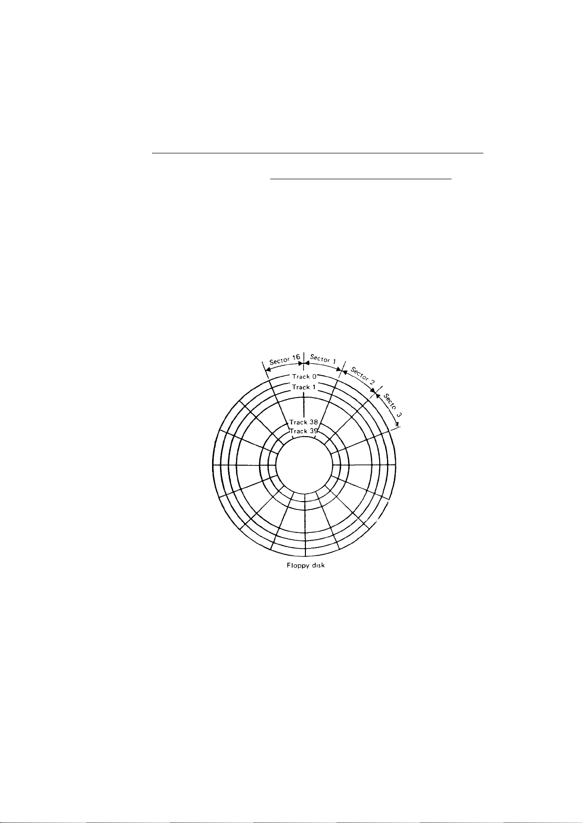
MZ3500
o MFM method (double density)
The MFM method writes data on the basis of the condì
tion metntioned below, and it yields a data density two
0 ^ 0 ^ 0 1Jl0
Input data
\ /\/\/\/\ /\ /\ /\ / \ / \ / \ /\ /
Write data
n
c c
n
(C) I) (Ü 1
nnn
I 3m 2m
Data that follows Data that precedes
The clock pulse (C) will be eliminated in above illustra
tion as there is no data preceding or following the clock
Because the data rate is 2ps for this method, it is
possible to obtain twice the density of the FM method
(4ps).
6) Media recording format
Media is formatted according to the IBM format
For Double side media, data is written on the front side
(head-1) and the reverse side (head-00)
times the data density of the MFM mode (The unneces
sary clock pulse is eliminated using this method )
1
JLJLJl
n
(C 1 '!) (Cl '!) ICI DU
1 > 1
^—
< I 1
-------
---------------------------------
(Condition) Clock IS written only when there is no data
1
1
1
0
0 0
Jl
nnn
(u ;d (u
1
----
►(
2m
NOTE Three types of write data cycle* (2i* j,<") i/is)
are used The read/write waveform is identical
to FM method
4 M
n
It)
Tracks, consists of 40 tracks, 00-39. (May also be called
cylinders)
Sector. 01-16
Recording density: 256 bytes/sector
54
Page 50

Shown below IS an enlarged view of data format
sequence Writing starts as soon as the index hole comes
through the index detect hole
Sector 01 Sector 02
ID ^ DATA ^ I Dt DATA
Hatched portion is
a recording gap
4
--------
1 D
AM
ID section--------^
TT
HH SS DL CRC
CRC
M 7 3500
1 Track
Fimi -.Pctor
-!S-
DA I A
CRC CRC
ID section CRC check code
“► Size of data section
(00) 128 bytes
(01) H— 256 bytes
-► Sector number
-► Head number
Head 0 (side 0)
(00) H -
• Head 1 (side 1)
(01 ) H -
{1
-► Track number
-► ID address mark which
begins the ID section
7) Formatting
To write the above format (ID section, data section, gap)
on an entire surface of a new floppy disk is called
formatting
Note 1 Formatting may also be called initialization. The
word "initialize" is also used as a software term to clear
the data section or to partition data area. Keep the
difference between formatting and initializing in mind.
Note 2 Unless formatting has been done on a properly
adjusted floppy disk drive unit, an erroe may occur on
another floppy disk drive unit
8) Data write procedure
Described next is the procedure to write data on the FD.
(1) The head is moved over the track to be written.
(2) The head is loaded
(3) ID section IS read and repeated until the desired
section IS reached
(4) When the desired ID section is found, data is written
on that area (DATA AM is also written )
(5) The data thus written is now checked if it was
written correctly (read after write) The respective
ID section IS read while the media makes a full turn
Data section
CRC check code
■ Data address mark
(or delete address mark)
NOTE The delete address mark
IS written to indicate invalid
data It IS often written on
a new floppy disk as there are
no valid data on it
(6) The sector of the identical ID is read and verified
with the write data Because of thr pad aftei Ari'e
capability the possibility of an error in the written
data IS quite low
9) Data read procedure
Described next is the procedure to read data from the
FD.
(1) The head is moved over the track to i ead
(2) The head is loaded
(3) The ID section is read and repeated until the desired
sector is reached
(4) When the identical IDsection is found, the d-itp m
that data section is then read
- 5Ó -
Page 51
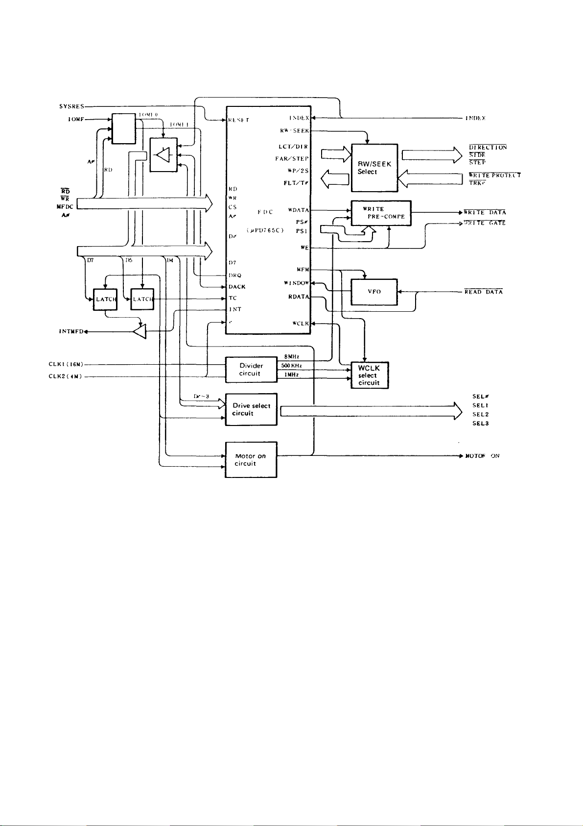
MZ3500
5-3. MFD interface block diagram
56 -
Page 52

5^. FDC (UPD765)
MZ3500
UPD765 pin configuration (top view)
KLSt I 0~
RDO—
WHO—
CSO—
AOO—
DBO
--—►
—►
1
►
2
3
4
5
6
7
8
9
10
11
12
13
14
15
16
I NDEXO
--------
►
------
17
18
19
20
I NTCV«
)fO-
GNDO-
40
39
38
37
36
35
34
33
32
31
30
29
28
27
26
25
24
23
*
------
22
21
—O Vcc
-►ORW/SEEK
-►O LCT/Dl R
-►O FLTR/STEP
->0 HOLD
—O READY
■O WPRT/2S1DE
FLT/TRKO
♦O WDATA
-►O USO
-►O USl
-*0 SYNC
—O RDATA
O WINDOW
—O WCLK
UPD765 block diagram
- kf AH'»
*1 KT 2'' 1 DF
- 1 SDF X
-n T TkKO
•^Efch
► H'X D
► S { DF
► LCT I)J R
►FLTK STEP
RESET ; Reset MFM
RD : Read SIDE
WR ; Write USO, 1
CS ; Chip Select WDATA
AO : AO PSO, 1
DBO • 7 ; Data Bus FLT
DRQ : DMA Request TRKO
DACK : DMA Acknowledge WPRT
TC : Terminal Count 2 SIDE
INDEX : Index READY
INT : Interrupt Request HDLD
0 : Clock FLTR
GND : Ground STEP
WCLK ; Write Clock LCT
WINDOW : Data Window DIR
RDATA : Read Data RW/SEEK
SYNC : VFO Synchronize
WE : Write Enable
: MFM Mode
; Side Select
: Unit Select
: Write Data
: Pre Shift
; Fault
: Track 0
; Write Protected
: Two Side
; Ready
: Head Load
; Fault Reset
: Step
: Low Current
: Direction
: Read Write/Seek
- 57
Page 53

MZ3500
UPD765 signal description
Pin No.
40
20
19
1
4 CS
13 ~ 6
3
2
18
5
14 DRQ
15
29, 28
26
Signal name
DB7 ~ DBO
I/O Function
Vcc
GND
0
RESET Set the FDC into an Idle state, and all drive unit interface outputs, except PSO. 1, and WDATA
WR
RD
INT 0 The signal used to indicate a service request from the F DC It is issued at every byte in the non-
AO
DACK
USO, 1
MFM 0 The Signal used to designate the operation mode of the VFO circuit When 0. the MFM mode is
-
-
1
1
I/O
1
1 Control signal to read data from the FDC via the data bus
1 The signal used to select the status register or data register of the FDC for access via the data
о FDC to memory data transfer request signal in the DMA mode
I
о Drive unit select signal, with which up to four drive units can be selected.
+5V
0V
Single phase, TTL level clock
(don't care), are set to low level In addition. INT and DRW outputs are set to low level DB goes
into an input state.
Validates RD and WR signals
Bidirectional, tri-state data bus
Control signal to write data to the FDC via the data bus
DMA mode, or upon completion execution of a command m the DMA mode
bus. When 0, it selects the status register When 1, it selects the data register.
The signal that indicates use of the DMA cycle During the DMA cycle, it functions identically
to CS.
assigned. When 1, the FM mode is assigned
24
39
36
27
38
37
35
34 WPRT/2 SIDE
17
33
16
30
25
21
SYNC о The signal used to designate the operation mode of the VFO circuit When 1. it permits reading
RW/SEEK о
HOLD
SIDE
LCT/DIR
FLTR/STEP
READY 1
INDEX
FLT/TRKO
TC
WDATA о Data written on the floppy disk consists of clock bits and data bits
WE о Signal to indicate write enable to the drive unit
WCLK 1
operation. When 0, it prohibits reading operation
Signal used to discriminate the read/write signal from the seek signal that used for drive unit
interfacing signal. When 0, it indicates RW When 1, it indicates
о Signal used to load the read/write head
о Signal used to select head #0 and head #1 for the double-sided floppy disk drive unit. When 0,
о When the RW/seek signal is operating as RW, the signal works as LCT which indicates that the
о When the RW/SEEK signal functions as RW, it works as F LTR which resets any fault condition
1 When the RW/SEEK signal is operating as RW, it furtction as WPRT which indicates that the drive
'
1 When the RW/SEEK signal is operating as RW, it works as FLT which indicates that the drive
1
it selects head 0. When 1, it selects head 1.
read/write head is selecting the cylinder above 43. When the RW/SEEK is operating as SEEK,
it works as DIR which indicate seek direction When 0. seek is made towards outer side
When 1, seek is made towards inner side
as the seek step signal.
Signal used to indicate that the drive unit is ready for operation
unit or the floppy disk is write protected. When the RW/SEEK is function as the SEEK signal
produces 2 SIDE which indicates that a double sided media is in use.
Signal to indicate the physical start point of the track.
unit is in a fault condition. When the RW/SEEK is operating as SEEK, it works as TRKO
which indicates that the read/wnte head is on cylinder 0.
Signal used to indicate the termination of a read or write operation
Data write timing signal which is 250kHz in the FM mode or 500kHz in the MFM mode
58
Page 54
MZ350C
P.n No
32. 31
23
22
Signal name
PSO. 1
RDATA
WINDOW
I/O
Signal used to either advance or delay the write data in writing under the MFM mode,
to obtain timing adjustment for reading. The WDATA signal is controlled as shown in
the table below
PSO
Read data from the drive unit consists of clock bits and data bits.
Signal created in the VFO circuit which is used to sample RDATA. Phase syncroniz
carried out in the FDC for RDATA data bits and WINDOW.
5-5. Data recording method
There are two ways of recording data; FM recording
method and MFM recording method.
2) MFM recording method
(1) Data bit IS placed in a middle of a bit cell.
(2) When the data bit is "0", a clock bit is placed before
the current bit cell. (See Fig. 1)
PSl
0
0
1 0
1
Function
FM MFM
Not changed
0
1
1
1) MF recording method
(1) Clock bit indicates a bit cell.
(2) Data bit is placed in a middle of a bit cell. (See Fig. i.)
Not changed
-
-
- -
LATE
225~250ns
EARLY
225~250ns
lULJUlJLJLJLJLJlJLn
[ 1
1 1
1 1
i n i
1 1
1 1
1 1
1 i
1 ■ 1
0
As seen from the above illustration, bit density of the MFM
recording method is twice the FM recording method. In
other words, data density of the MFM recording method
doubles that of the FM recording method. For the
. 1
i
n 1 r
1
1
1
1
> i 0
1
1
1
1 r
0 0 0 1
5-6. I/O port in the MFD interface
I/O port used in the MFD interface is as follows.
U-BUS
IOMF#F9-AO OUT
D7
D6
I/O
DACK
ME
SCTRL
D5 TC
D4
D3 SEL3
OUT
TRIG
IOMF#F8-AO 1)2 SEE 2
1)1 SELl
DO SELO
D2
D1 IN
DO
M . ON
I NDEX
DRQ
(FM recording method)
r
Model 3500, only side 0 of track 0 (128 bytes/sector) is
written in the FM mode and rest of other tracks are
recorded in the MFM mode.
Used for data transfer between the CPU and the FDC.
INT from the FDC is output enabled on INTFD.
FDD select signal output is enabled.
TC to FDC.
Trigger (motor on) of the timer (555)
Selects FDD 3
Selects FDD 2
Selects FDD 1
Selects FDD 0
ON/OFF state of the motor
INDEX signal from the motor
DRO from the FDC.
• (MFM recording method)
- 59
Page 55

M 7.3500
5-7, Precompensate Circuit
<IT E DA TA
Set the counter to 200ms.
(Actually, slightly longer than 200ms.)
PS1
PSO
0
0
1
0
1 0 1
WDAT.A.
8MHz
CLOCK
EAKLY-
NOMAL-
_r
lJnJljn_riJn_rL-rLr
LATE-
The precompensate circuit is used to compensate the peak
shift before writing.
The FDC sends out the compensation rate to PSO and PS1
and the data bit location is shifted according to this signal.
With issuance of WDATA, the value dependent on PSO and
PS1 is set in the LS163. (See Table 1.) For instance, when
both PSO and PS1 are low, it will set "1101(D)" to the
LSI63, counted up by the 8MHz clock, and QB is sent out
When it becomes "1110, 1111". When in EARLY (PS0=
"H", PS1="L”), the value "1110(E)" will be set to the
LSI 63 so that the output is issued 125ns earier than "not
changed". The QB output, however, will be supplied for a
period of two clock cycles.
FM MFM
Not changed
-
- - -
Not changed
LATE(125ps)
EARLY(125iis)
(Table 1)
(Fig. 3)
Value of LSI63
1101
1100
1110
Media is present. Media is not present.
5-9. Controls during read, write, seek, and re
calibrate
Above operations are all controlled via the FDC.
1) Control during read and write
2) Control during seek and recalibration
SEEK (or RECALB)
5-8. Media detection
Insertion of a media on the MFD is detected via the signal
INDEX from the MFD. Since it takes 200ms for the media
to make a full turn, "NO MEDIA" is detected signal
INDEX does not appear within 200ms.
- 60 -
Page 56

In the case of the MFM method, need to trace cycle fluc
tuation IS further increased, as a peak shift is apt to occur
because there are three write data cycles.
(Peak shift). Data read cycles fluctuate as the flux change
point IS moved forwards or backwards.
(VFO circuit): Variable frequency oscillator
Polarity inversion
_________
|~|
__________
Polarity inversion
Write pulse [] fl d fl R
Polarity inversion
Write pulse _n
_____
Mzasoo
TL
Write pulse
When the output v"aveform is observed after writing a single
pluse on the floppy disk, the waveform show in (a) appiears.
Shown in (b) is two pluses of 4ps interval.
5-10. VFO circuit
1) Purpose
String of data
pulses from the FDD.
Data window
String of
separate data
J
Deviation in the peak point is called peak shift. Since pluse
intervals of the MFD in actual operation are 4ps, Bps, and
8ps, the largest shift takes place when a pluse appears Bps
before or after 4ps, as shown in (c).
_rL_
1
_____
T
n
- 61
Data from the clock or data portion must be differentiated
when read from the FDD. For this purpose a window pulse
is used. In order to increase read tolerance, the VFO circuit
carses the window to trace phase changes in the read data
that take place during a floppy disk drive motor speed
change.
Page 57
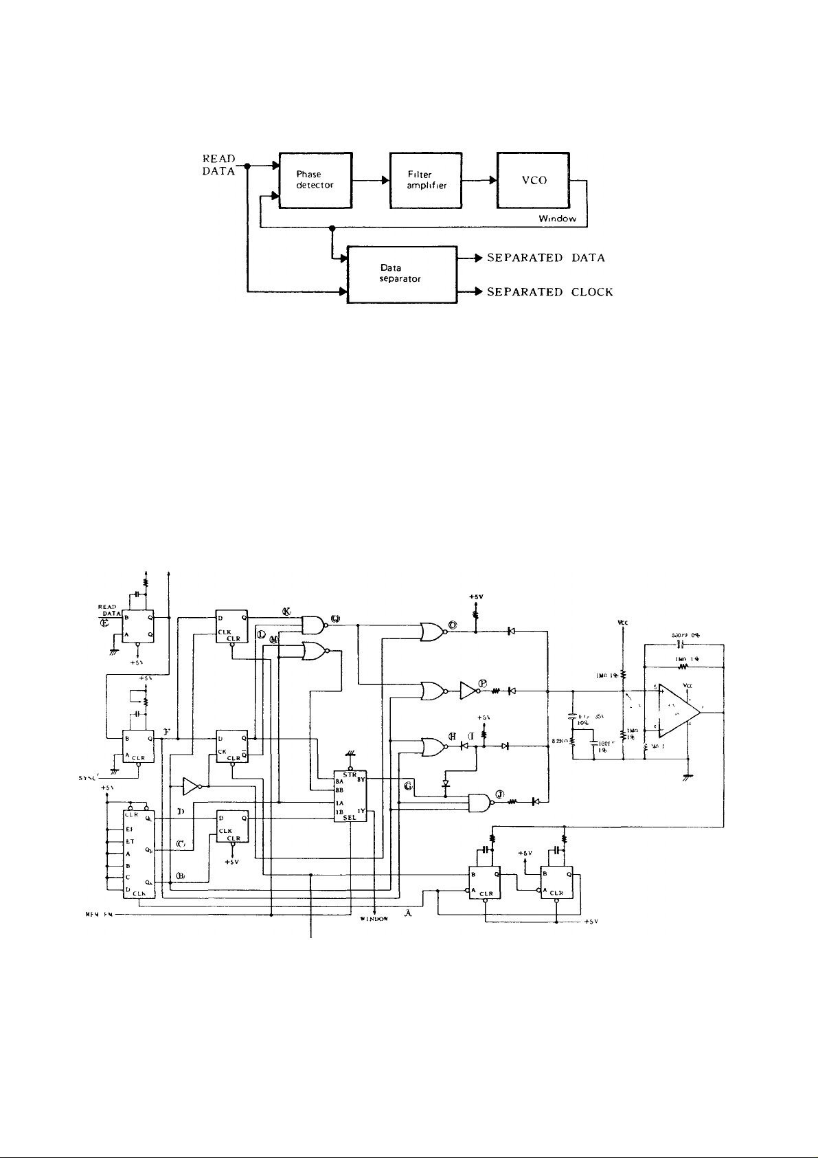
MZ3500
2) VFO circuit configuration
The VFO circuit has the following capabilities.
(1) Two modes; MFM and FM.
(2) The VFO circuit operation is suspended during the
SYNC field located before the ID field and data field.
(3) After suspention, the VFO circuit will synchronize
with the read data (timing is affected by a speed
change in the FDD). Fluctuations in an individual bit
that may be seen (peak shift are ignored.
+5V RtAD DATA
VFO circuit
- 62
Page 58

MHz
01
OQA) __|~
M -- 3.1
MFM Mode
Nomai
STD
Eary
OQB)
1_
©.
©.
©
©"T
o_
©~
©.
©.
©
Delay
®"1
©__
© —
©_
©
©
©—
____
___
63
Page 59

MZ3500
FM mode timing chart
A 4M
WINDOW
Normal
B(QA) J 1
C(QB)
D(QC)
E
F
L
O
P
F
______
I L
_J L
_r~L
J
1_
“L
L
Advanced
O
P
L
K
Delayed
Q
O
P
Does not trace i l^is.
1
____
1
____
r
r
r
64 -
Page 60

5-11. Media format
0 tr.ick
^<¿3500
Sector MASTER
Boot, OS information
(See Fig 1)
BOOT
BOOT
BOOT
C5 , D9 . D4 , Cl , D7 . 40
E5 , D6 , D3 , F 1 . E2 , C8 , C I , D9 , D7 , 4 0 '—^ 4 0 , D4 (40onone side), 40''^F 1
MAP: Nine sectors for the media of
34 tracks
Area. 10th sector is also a MAP area
10
for the media of 40 tracks
00
MAP
Area
BLANK MEDIA
00
00
00
00
40
FF
FF
16
15
16
FF
E5
E5
E5
E5
c
o
- 65
Page 61

M/asoo
Track 0, sector 1 information (SBACIS) (Fig 1)
AA 1 C
00 ' 00
02 I 00
04
-------1-------1-------1------1-----48'i00'48lo4'02'oo!oiloi
00
1-------]
-------1-----
System media
Track SIDE Sector M
Drive unit specification
------1----
: 02)0 1
; 1 0
SIDE Sector N No of
T rack
No of
0 . Single density, other than front side, track 0.
N
1 . Double density, other than front side, track 0.
SIDE =
No of data transfers 1NT= [IOCScapacity/1 k] +1
0 . Side 0 (front side)
1 Side 1 (reverse side)
01 ■ 01
1
1
No, of sectors | Start address
Load address No of data transfers
BOOT
1
i 1 0
1
FF '
END
1
t
T Tilt k S 1 Dl’ Snc tor N
SUB IOCS-
0 track 8 sector
FF No ALOAD command
80 File specification only
01 With operand
I Fail name (8 bytes) Expander Volume name
(3 bytes) (8 bytes)
Drive NO
Channe I
A (tr)
B (I )
1
I 1
All "F” when ALOAD command
ALOAD
Status line No label
(8 bytes)
(Bbyles)
Contents of X register
When used for the line number (when line No 123)
These three bytes are in effect
IS not on
34 35 36 3b>iesfj%
00 01 23
When used for a label (Wight bytes are m effect and rese are )
34
3C
A B C n i'i'
- 66 -
Page 62

о Мар information
М7 350?
о track 9 sector
О track 10 sector
FFH
I 71!
FFH
FFH
8e>H
FFH
128 blocks are controlled
by one sector.
ООН ~ 7FH
80H: End of link
FEH; Links to next map,
and the starting
block number.
Indicates the byte position
from the top of directory.
i t
00
01
02 0\ FF FF
29 30 31 У
FF FF
FF
t
MAPNa
Block NO
Starting block number (directory)
- 67
Page 63

MZ3500
o Block number allocation
The program and data areas are located after Track 2
1 block = 2K bytes (8 sector)
(Double side) (Single sided)
Block No
track
Front
Reverse
track
Block No
Front
2 BO B1
3 B4 B5
I
38
39
Each track is blocked in the following manner:
1 sector
3 4
5
;
(
13
15 sector
o Track 1, Sector 1 information (CP/M)
0 5
AA
B144 B145 B146 B147
B148 B149 B150 B151
( 2KX 152 = 304K )
2 sector
6
■ 1 block j
(
14
16 sector
SIDE SECTOR
TRACK
B2 B3
B6 B7
2 BO B1
3
38
B2 B3
B72 B73
39 B74 B75
( 2KX 76=152K )
1 block
------1
---------
-----------1----
SECTO
N
R NUM
BER
1
1
1
______1_____1______
10
DATAT
1
iANSFl
1
ER NU
MBERlI
1—
TRACK
SIDE
SECTOR N
15
Drive unit
specification
Represents the
system media [•
SIDE
Nos of data transfers = INT [IOCS capacity/1 K] + 1
• Sub IOCS can be divided into either blocks If divided to
0 Side 0 (front)
1 Side 1 (reverse)
less than eight blocks, the block that follows
---------------------
20
SECTO
RNUM
TRACK
BER
Single density (front, Track 0)
1 Double density (other than front. Track 0)
SIDE SECTOR N
SUB-IOCS
SECTO
R NUM
BER
BOOT
Load address Start address
68
50 51
TRACK SIDE SECTOR N
SECTO]
R NLISA
BER I (
Indicates
the eiKi
Page 64

6-1. General specification
MZS500
6. R232C INTERFACE
Input/output format
No of channels
Code used
Baud rate
Transmission system
Synchronization method
Communication control
procedure
Data format
LSI used
RS-232C bit serial inpul/output
1 channel
JIS 7-channe(/JlS 8 channel
110 to 9600 bits/sec
Half-duplex
Start-stop
Non-procedure
Stop bif 1/1.5/2, with or without
even or odd parity.
8251 AC or 8253C-5
(Programmable Interval Timer)
6-2. Data transmission format
7-bit,
with parity
7-bit,
without parity
Start bs\
Start bit
gO g' 2^ 2® 2^ 2^ 2®
Data bit (7 bits) Parity bit Stop bit (1 or 2 bits)
------Y------Data bit (7 bits)
Stop bit
8*bit,
with parity
8-bit,
without parity
Example: 7-bits, even parity, 1 stop bit
Stop bit of preceding data
Start bit
Start bit
Start bit
Data bit (8 bits) Parity bit Stop bit <1 or 2 bits)
Data bit 18 bits)
2° 2' 2^ 2® 2'* 2® 2®
7-bit data {26H}
Stop bit (1 or 2 bits)
Panty bit
Stop bit
Start bit of
succeeding data
71
Page 65
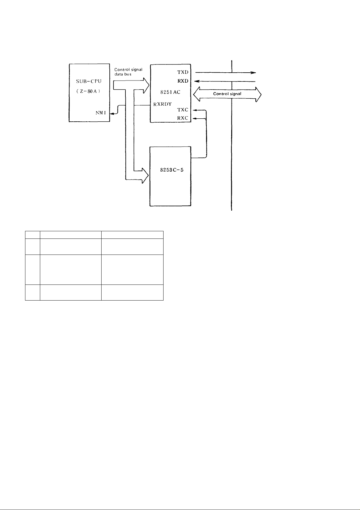
MZ3S00
6-3. Block diagram of the interface
Peripheral
6-4. System switch functions
ON
Causes an error when the
SW5
ER signal is low or open
during data output.
Always high when power is
SW6
on to the main unit.
Causes on error when the
SW7
PO signal is high during
data output.
6-5. 8251AC controls
There are two control words for the 8251 AC.
(1) Mode instruction: Defining general operational para
meters, such as unit, stop bit, etc.
(2) Command instruction: Defining status words used for
actual operation, such as send/receive enable, etc.
1) Definition of generation operational parameters
• Baud rate
• Character size
• Even/odd/off parity assignment
-•Stop bit size
'Corresponds to channel command of BASIC.
ER signal is disabled.
The CD signal is set high
while data output, but
would not be set high
when the echo-back
furKtion is selected for
the host computer.
Polarity is inverted.
OFF
c
START
8251AC internal reset
8251AC mode instruction
J
72 -
Page 66

2) Data output control
MZ3500
- 73 -
ERROR 101
Page 67

M/ 3S0U
3) Data input control
Read one data
/Clears the data before \
Vthe start of the receive command /
74 -
Page 68

MZ3500
6-6. 8253 Controls
Baud rate of this interface will be determined by the clock
output of the 8253. The 8251 is configured such that its
baud rate is 1/16 of the input clock and has the following
relation between the 8253 output clock and the baud rate:
8253 input frequency: 2457.6kHz
8253 Mode set: Mode 3(rec’angle waveform rate generator)
Control signals
Signal name
Symbol
Transmission enabled
Data set ready DR
Carrier detect
Beady
READY
Equipment ready ER
Paper out
CS “* Peripheral When high, data input from a peripheral is enabled.
CD
PO Peripheral
IN/OUT
-♦ Peripheral
Peripheral
Peripheral
•*- Peripheral
When low, data input from a peripheral is disabled.
Goes high when power is on to the interface unit.
(SW6-ON) High at all times when power is on to the interface unit.
(SW6-OFF) Goes high only when data is on output.
Data output from the interface is enabled.
(ON) Data is output from the interface.
(OFF) Waits for data output.
NOTE: A maximum of two bytes are output after the signal goes from high to low
Indicates that the peripheral is ready, it results in an error if low or open when data
is sent from the interface. This signal will be invalidated when the SW5 is turned
off.
(SW7-ON) Causes an error if set high during data output.
(SW7-OFF) Causes an error if set low during data output.
state.
Baud rate
1 1 0 ,t -
825 3
Output frequency
1 7 60hz
8253
1 3 9 6.3 6
300 4 800 5 I 2
600 9600
I 200
24 00
1 9200
384 00
4 800 76800
9 6 00
153600
Function
Parameter
256
128
64
32
1 6
6-7. Description of LSI's
1) UPD8251AC (Programmable Communication Interface)
The UPD8251A is a USART (Universal Synchronous/
Asynchronous Receiver/Transmitter that was specifical
ly designed for data communication.
The USART receives parallel data from the CPU and
converts it into serial data before transmitting. Also,
serial data is received from an external circuit and trans
ferred to the CPU after converting it into parallel. The
CPU can monitor the current state of the USART at
any time (data transfer error, and control signal of
. SYNDET and TXEMPTY.
.-eatures
• 8080A/8085A compatible
• Synchronous/asychronous operation
• Synchronous operation
5 — 8 bits character
Clock rate: baud rate x 1, x16, x64
BREAK character generation
Stop bit; 1, 1.5, 2 bits
Error start bit detection
Automatic break detection and operation.
• Baud rate: DC — 64K baud
• Full-duplex
Double buffer type transmitter/receiver
• Error detect
Parity, overrun, framing
• Input/output TTL compatible
• N-channel MOS
• Single -r5V supply
Single phase TTL level clock
28-pin, plastic DIP
Intel 8251 A compatible
T)^ O-
RXRDY
D7-D0C>#-
RESETO
75 -
Pin configuration (Top View)
D2 04
--------
^
D3 O*RXD O—
GND O—
D4
04-
D5 04-
D6
04-
D7
04-
----
10 -I
WHO—
C -D O
cs o
RD O
04
11
12
15
14
■►C
Internal data bus
Block diagram
.28
♦ODl
,27
♦ODD
26
—OVCC
25
D4
-ORXC
.24
-►ODTR
-►Orts
22
-ODSR
21
-ORESET
20
■4^—OCLK
19
-►OTXU
18
-►OTXEMPTY
[04lZ.„-o CTS
,16
-►O SYNDET BD
15
-►OTXRDY
>OTXD
¥CTXK iJ
>otxe
>4
----
X)RXRI)/
OK^
SYMJhl HI)
Page 69
MZ3500
D0-D7
RXD
WR
RD
C/D
CS
DSR
DTR Data Terminal Ready (OUT)
RTS
CTS
TXRDY . Transmitter Ready (OUT)
TXC
TXE
RXC
SYNET/BD : SYNC Detect/Break Detect (IN/OUT)
2) UPD8253C-5 (Programmable Interval Timer)
The UPD8253-5 is a programmable counter/timer speci
fically designed for the 8-bit microcomputer system.
It consists of three sets of 16-bit counters that operate
under a maximum counter rate of 4MHz. Timer and six
operational modes are programmed to be used for a wide
range of microcomputer system timing control.
Features
• Z-80 compatible
• Three sets of 16-bit counters
• DC-4MHZ of count rate
• Programmable six operational modes and timer
duration
• Choice of binary counter/BCD counter
• N-channel MOS, input/output TTL compatible
• Single -t5V supply, 24-pin DIP
• Intel 8253-5 compatible
Pin configuration (Top View)
Data Bas
Receive Data (IN/OUT)
Write (IN)
Read (IN)
Control/Data (IN/OUT)
Chip Select (IN)
Data Set Ready (IN)
Request to Send (OUT)
Clear to Send (IN)
Transmitter Clock (IN)
. Transmitter Empty (OUT)
. Receiver Clock (IN)
D7 ' DO
A1
A—\ Data bus
\—^ buffer /
Read/
AO
CS
write
logic
Control
word
register
D7~D0 Data Bus (8 bit)
CLKN Counter Clock Inputs
GATEN Counter Gate Inputs
OUTN Counter Outputs
RD . Read Counter
WR Write Command or Data
CS Chip Select
A1~A0 : Counter Select
Vcc . -1-5 Volts
GND . Ground
Block diagram
Ico
Vr/
C=^
w
Counter ^
# 0
Counter
# 1
Counter
# 2
-------------
<
------
^
---------
<
---------
------
*
------
CIKO
(,MhO
-►(n 1 0
Ci K 1
OAl h
-► ()l I 1
Cl h2
GAlt2
-►01 T2
CLKOO
OUT 0 04
GATEOO
GNDo
oVcc
OWR
OCLK2
>OOUT2
OGATE2
OCLKl
OGATE1
li—K)OUTl
76
Page 70

825 1
MZ3500
8 2 5 1
chip addresstOOOl/xxxxl
IN
OUT
8253
8253
chip address[0010/xxxx]
OUT #
IN #
#1X
2XH
CLK
DSR
IN
IN
in R OUT
CTS 1 N
ris
TXD
OUT
OUT
TXRDY N.C.
TXE
TXC
RXD
N.C.
IN
IN
RXRDY OUT
RXC
IN
SYN/BD N.C.
CLKO
GATED
OUTO
CLKl
GATEl
OUTl
CLK2
GATE 2
OUT 2
IN
IN
OUT
IN
IN
OUT
IN
IN
OUT
2.45MHz clock
DATA SET READY
DATA TERMINAL READY
CLEAR TO SEND
REQUEST TO SEND
TRANSMITTER DATA
TRANSMITTER CLOCK
RECEIVE DATA
RECEIVER READY
RECEIVE CLOCK
2.45MHz
Vcc
To TXC, RXC of the 8251
2.45MHz
From OUT2
MUSIC
2.45MHz
Vcc
To GATE 1
READY
CS
PO (MPER SUT), ER
CD
RD
OUT 0 of 8253
SD
To 3iil>CPU of Ni^
8253 OUT
INTO TO MAIN FROM SUB
POWER ON RESET
SOO S1W(lORQ-WR of SUB)
INTR=L(FROM MAIN)
I NT TO SUB FROM KEY
STK= ( L)
INTO
H
L
H
77 -
Page 71
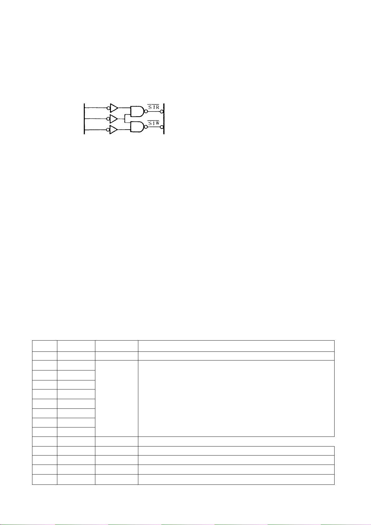
M 7. 3500
7-1. Printer interfacing circuit
AS 4 - ASS AS6 ■ AS7
7. PRINTER INTERFACE
AR Chip S03
Kl)
lOKQ
WR
A1
Z80
AO
SUB
CPU
7-2. Parallel interfacing signals
Pin No. Signal name
1 STROB
3
5 DATA 2
7 DATA 3
9
11
13
15
17 DATA 8
19
21
23
25
27
DATA 1
DATA 4
DATA 5
DATA 6
DATA 7
ACK
BUSY
PE
PDTR .
SYSRES
Ch 1 p
ScU’i t
Iode r
IN/OUT
- PRINTER
PRINTER
- PRINTER
* PRINTER
- PRINTER
- PRINTER
- PRINTER
CS 8255
KU
PAO
PAl
<o
<i>
PA2
WR
PA3
A1
PA4
AO
PA5
PA6
PA7
4^
PCS
PC6
----
PC 7
PCO
PCI
PC2
DSO
DSl
US 2
s.
DS3
DS4
DS5
DS6
s.
LS244
<<1-
-VSAA-
DS7
2, 4, 6,... 28 are GND.
Above pin numbers are of the model-3500 main unit.
Function
Data is transfered to printer when STROB is high.
Data output to the printer
Indicates the end of character input or function input i
When high, it enables to receive data
When high, it indicates paper empty
When high, it indicates the SELECT mode (receive enabled).
Reset signal, normally high
78
DATA I
DAT A2
DATA3
DATA 4
-(d) DATA5
DATA6
_(0) UATA7
DATA8
STROBE
ACK
@
Busy
-® PE
PDTR
Page 72

7-3. General description of the parallel interface
The 8255 is used for the LSI to control the parallel inter
face. The 8255 can be set in the following mode.
/PORT A: MODE 0
( PORT B;MODE 1
V
PORT C : Output
7 4. Data transfer timing
MZ3-0C
Because it is not possible to directly sense the ACK signal as
It uses interrupt for key processing and RS232C input, the
ACK signal is latched by means of the OBF pm function
PRINTER: MZ-1P02, MZ-1P03CE330P, 331P, 332P
* Broken line in the above figure represents timing for the
CE-330Pand 33IP.
*For detail of timing, refer to Manual provided with
printer.
7-5. General description of control software
Set the 20 second counter.
- 79 -
ERROR
Page 73
M / 3500
7-6. I/O port map
8255 ON SUB CPU BUS
8255
chip address(CX)11 /xxxx]
Group A: Mode 1
Group B: Mode 0
PA7
N.
PA6
i‘A5 DATAS
PA4 DATA 5
PA3
PA2 DATAS
CÌ
o
PAI
c
PAO
>
PC7
PC6
PC 5
Output
>
OBF outpu
ACK inputi
N
PC4
PC3
PC 2
INTR NOT USE
N
PCI
PCO
PB7
PB6
O
T3
ro
o
c
PB5
PB4
Output
PB3
PB2
PBl CO
PBO
DATAS '
DATAT
DATA4
DATA2
DATAI
ACK T-SET
ACK
STROBE ^
MUS 1 C , sustain
ACKC '
STC
DC
P/M
CG selection
SRDY
CLK
Din
C2
CI
Clock
STRB -
Printer
Keyboard
Sub CPU READY
INPUT PORTC74LS2443
74LS244
port addressÌOlOO/xxxx]
CDS7 :
CDS6D
CDS5D
CDS4D
CDS33
CDS23
CDSl 3
COSO 3
HLT KEY
STK D
DK J
Keyboard
PDTR -1
PE
Printer
BUSY J
Reads the 8255 OBF (PC7)
output or timer output.
- 80 -
Page 74

8-1. Clock circuit
1) Schematic
M 2 350o
8. OTHER INTERFACES
2) Clock timing
- 81
Page 75

MZ3500
3) a^PD1990AC
Block diagram
-O DOU'l
-<3 ri>
Command specification
Cl CO
C2
0 0
0
0
0
0 Register hold
1 Register shift Data input/output
0
1 0
1 1
Input/output format
Command Description
Holds 40-bit S/R
Time set
Time read
(LSB)
^ Seconds —^ ^Minutes—^ ^ ^Houre J ^ ^—Day —^ ‘-Month
Data of the 40-bit S/R is
preset to the time counter.
Data in the time counter
is read to the 40-bit S/R.
Example; In the case of 10 o'clock, 25 minutes, 49 seconds, July 30th.
DOUT Data Shift
1Hz
[LSB] Output of LSB Possible
(LSB) Output Not possible
[LSB] Output
1
Not possible Data retention
Shifts in synchronization
with the dock
Not possible
(MSB)
Note
- 82
Page 76

8-2. Vo ice in put /ou tpu t ci rc uit
MZ,"500
Music output waveform
• Tonal signal
OUT1
• Sustain
PC4
2SC458
emitter
• 2SC458
collector
♦ Speaker
• GETEl
output
•
- 83 -
Page 77

M/3500
8 3. Expansion and interrupt (See 3-(2)-4 for interrupt)
1) Options and expansion units
Optrons not requiring expansion unit
MZ 1K01
1001 14" medium resolution color CRT
1D02
•1D03
-1S01 14" CRT tilt stand
-1S02 12" CRT tilt stand
•1X02 Light pen
-1P02 80-character prmte
-1P03
-1P04 Color injket printer
CE-330P
-333P 136-character printer
-331M Optional MFD drive unit
-330X
MZ-1F02
-1F03 Optional MFD drive unit (single deck)
-1R03
-1R05
2) Expansion unit
Signal assignment by slot
J!S keyboard
12" high resolution green CRT •1E03 SFD 1/F
12" high resolution color CRT
80-character printer
Plotter
Optional MFD drive unit
Graphic board
MZ-1E01
-1E02
-1F05 SFD unit
-1R06
RS232C 1/F 0
GP I/O ®
RAM
84 -
Page 78

8 4 System SW1 (DIP SW) (User operative through the cabinet bottom)
M7 3500
No
Signal name
SW1
SW2
SW3
SW4
SW5
SW6
SW7
FD1
(SW8)
P/M
(SW9)
Function
Printer select
CRT select
Choice of decimal
point output
format
RS232C
assign
Key shift mode
setup
Choice of CG
for display
Position Polarity
ON
OFF
ON
OFF
ON
OFF
ON
OFF
ON
OFF
ON
OFF
ON
OFF
ON
OFF
ON
OFF
Description
SW2
ON ON CE332P
SWl
#47 pin of MMR
OFF ON MZ1P02
ON OFF
OFF OFF
High resolution CRT (MZ1D02, MZ1D03)
Medium resolution CRT (MZl 001, M21D06)
A period IS output for a decimal point
A comma is outputted for a decimal point
Low state or open ER signal during data output
will result in an error
The signal ER becomes invalid
CD IS high as long as power is on to the mam
unit
CD goes high only during data output Flowever,
It would not go high if the echo back function is
on the host side
An error IS cause when the PO signal is high
during data output
Polarity IS inverted for the above
Normally in capital letter, but in small letter
when shifted
Normally small leter and in capital letter when
shifted
3500 CG will be assigned when the 200 raster
CRT IS in use
2000 CG will be assigned when the 200 raster
CRT IS in use
102824
-
#48 pm of MMR
#51 pin of MMR
#52 pin of MMR
To CTS, DSR
of the 8251
To CTS of the
8251
#54 pin of MMR
(FDD
P/M signal
(To A3 CG)
Dip switches (A) and (B) located on the PWB are used for
servicing the MFD or for other machine service and there
fore the user is not supposed to use these switches In
addition, these switch must be used when either the CE
330M or 331M IS used as the expansion MFD
DIP SW (A)
No Stgnal n^ne
SEC
1
(SW1A)
FD2
2
3
4
(SW2A)
FD3
(SW3A)
SRQ
(SW4A)
44 pm of MMR
56 pm of MMR
58 pm of MMR
Bus request
to sub-CPU
1
OFF OFF OFF When SH m use
ON OFF OFF When DH m use
OFF
ON ON OFF
OFF
ON OFF
OFF
ON ON ON
DIP SW (B)
No
Signal name
1
2 SW2B
SRES
(SW1B)
SUB CPU
reset signal
SUB CPU BUS
select signal
*1 Test program is loaded and executed
*2 Provided for the test of the MFD interface The
Used for an individual test of the CPU PWB When these
three switches are turned off altogether, it makes the
sub CPU operated independently To be used in th ON
condition under a normal situation
2 3
ON OFF
OFF
ON
ON
—
—
Use of the CE330M as an expansion unit
Use of the CE331M as an expansion unit
ON ON Check mode * 1
Check mode *2
read/write test is carried out for the expansion unit
Page 79

MZ 3500
OFF
ON
OFF
ON
OFF
ON
DIP SW(A)
1
2
OFF
OFF
OFF
OFF
ON
ON
X]
Can be in either state
3
OFF ON ON ON
OFF ON ON ON
ON ON ON
ON ON ON
ON ON ON
ON ON ON
X
4
OFF OFF
DIP SW(B)
1
2
Switches are set in this manner before shipment of machines this us the
single-sided minifloppy disk drive.
Switches are set in this manner before shipment of ,
machines that use the double-sided minifloppy MZ3540
disk drive. ' ' ’
ON
ON Switches are set in this manner when the DH is used for the optional MFD
ON
ON Test mode *2
OFF Individual CPU PWB test
Switches are set in this manner when the SH is used for the opiiunal MFD
T est mode * 1
86 -
Page 80

1. BLOCK DIAGRAM
M Z 3500
9, POWER CIRCUIT DESCRIPTION
A. +5V and +12V supplies
1. Functions
a. Supply voltage is first rectified in the rectifier circuit
and sent out to the switching regulator via the over
current detector provided in the overcurrent protect
circuit.
b. Next, the voltage is converted to the +5/-H2V output
in the switching regulator and sent out to the noise
' Nfilter.
c. Change in the switching regulator output voltage is
sensed by the control circuit and is fed back to the
switching regulator after being amplified in the amplifier
located In the control circuit, for maintaining the output
voltage to a constant level.
d. The signal from the oscillator is supplied to the switch
ing regulator through the control circuit for driving the
switching regulator.
e. For prevention of overcurrent, the protect circuit is used
for stopping the oscillator when an overcurrent is met,
and it makes the switching regulator to halt in order to
shut off +12V/-r5V supply.
2. Description of each block
a. Overcuirent protect (control/protect) circuit
When an overcurrent is met in the -r5V/-rl2V circuit, it
causes to increase the voltage at both ends of the over
current detector resistor R1, which in turn causes to
increase the Q3 collector current, for, there arises larger
voltage difference between the emitter and base of the
(Block diagram)
b. Oscillation circuit
-12V
Output
transistor Q3. This makes the gate voltage of the thyris
tor increased owing to activation of SR. Witf. activation
of SR it makes the oscillator voltage dropped to the
GND level at the point "a" to stop oscillation, which
also makes the switching regulator stopped by the de
activation of the transistor Q5 oscillation. This causes
the transistor Q5 inactive, and it shuts off the -r5V/
+12V supply,
As the Q1 emitter voltage is at almost GND level whethe transistor Q1 is active, the Q2 base voltage tem
porarily drops close to the GND level by means of C
which in turn makes Q2 inactive and the Q2 emittei
voltage increases.
Then, the Q2 base voltage comes to rise as C6 begins to
be charged through R6, and the transistor Q2 starts to
activate again. With activation of the transistor Q2, the
Q2 emitter voltage starts to drop and the Q1 base
voltage is temporarily dropped by means of C5, to shut
off the transistor Ql, which causes to increase the
transistor Ql emitter voltage.
Next, as C5 is charged by R5, it makes the Ql base
voltage increased which puts the transistor Ql into
activation. In this manner, transistors Ql and Q2 are
alternately turned on and off to keep oscillating.
C5 and C6 are charged through R5 and R6 by on/off
action of the Ql and Q2, and discharged through Ql and
Q2.
6,
- 87 -
Page 81

M 7,3500
1 +5V
^
---
or
J +12V
• VR IS the+5V or+12V adjusting VR.
• D3 IS provided to discharge current from Cj after power off.
- 88 -
Page 82
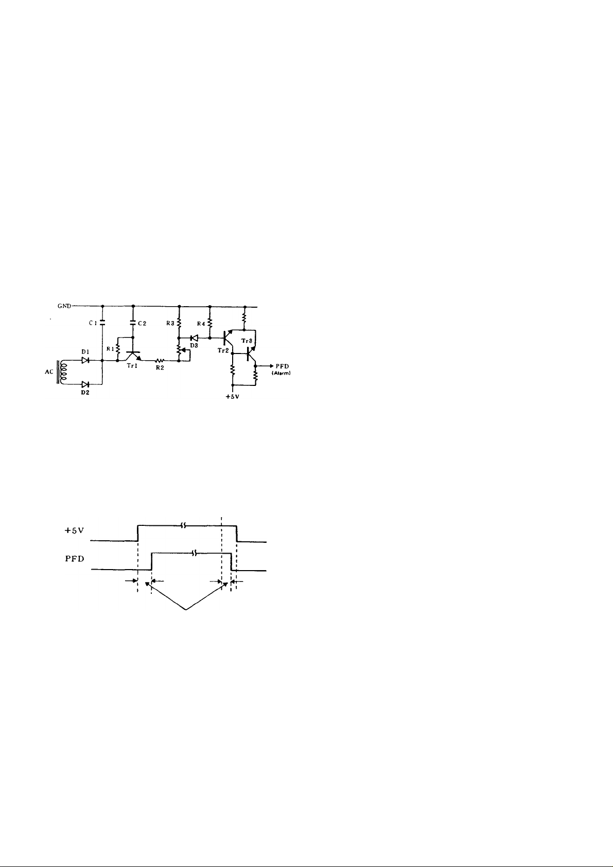
c. Power switching circuit
As the signal from the oscillator is amplified through Q7
to Q6 to change current to the transformer T2, it causes
voltage to appear on the base of Q5 (one of components
is cut by Dl), so that the transistor Q5 begins to per
form switching operation in synchronization with the
oscillation frequency. As Q2 is switched, current is
supplied to the emitter side of the transistor Q5, which
produces smoothed voltage through the capacitor Cl
and the coil L2. The circuit composed of D4 and VR1 is
the reference voltage for the -h5 or -H12V supply, which
is used to control the emitter current flowing to the
transistor Q9. The current supplied from Q9 is used to
create Tr3 inactive by the delayed Cl and C2 voltages
which supplied from Tr1-R2-VR1-D3. It goes high with
deactivation of Tr3.
3. Alarm circuit
(Alarm generation circuit)
M2 3500
When power turns off, the voltage accumulated in Cl
and C2 are supplied to the base of Tr2 via Tri ... and
D3, so that Tr2 is kept active and Tr3 inactive for some
times after power off.
Timing chart
SW
ON
- 89 -
Page 83

MZ3500
10. MZ1K01 KEYBOARD CONTROLLER CIRCUIT DESCRIPTION
10-1. Specification of keyboard control
1) Input Buffer
Capacity: 64 bytes
• Key-in data is written to the input buffer first, and is
supplied to the CPU, byte by byte.
• When an overflow is detected, the overflow code is
affired to the key-in data already sent, before being
sent to the CPU.
2) Rollover
• 2 key rollover (exemption in the CTRL mode)
(Entry of the second key depression can be accepted
even if more than one key is pressed at same time.)
• Simultaneous depression of more than three keys is
ingnored.
3) Key bounce
15msec (Key spec is 5-10msec)
(Indicates unstable state as shown in Fig. 3-2 that key
signal does not turn off immediately after releasing of
finger from the key.)
4) Key
5msec (norma), 20msec (max),
15msec (allows for key bounce)
5) DEF Key
Twenty definable keys are available in combination with
the CTRL key.
DFK1-DFK10
DEF1-DFK10 in conjunction with the CTRL key
[
- - - (DEFIB-DEF10B)-
6) Handling of functional symbols and graphic symbols
See the code table.
7) Use of the CTRL key to discriminate RUN and CONT of
the DEB key.
Push the DEB in conjunction with the CTRL key to
start running.
8) Handling of special codes
COPY command: CTRL j 1 | (ten key)
Escape
BRK
--------------------
9) PRO/OP
Sent to the CPU after power on and when PRO/OP is
changed.
10) HOME key
CTRL HOME] Returns home after clearing the
---------------------
---------------
CTRL |Ci^
CTRL I CONT]
_____
HOME Only the cursor returns home.
(DEF1A-DEF10A)
----------
(DEF1B-DBF10B)
display screen.
11) One-step commands
CMD 1 •
CMD 2
CMD3
CMD 4
CMD 5 ■
CMD 6 •
CMD 7
CMD 8
CMD 9 •
CMDO
CMD A
CMDC
CMD D
CMD F
CMD K
CMD L
CMDO
CMD R
CMD S
CMD U
12) Mode indication on LED
ASCII
13) REP
Key repetition will take place when a key depressed for
more than 0.64 second. Entry of other keys is permitted
during key repetition. When two keys are depressed at
the same time, an alternate key entry will not be
accepted. This rule does not apply to simultaneous
depression of more than three keys.
DISP
PRINT
INPUT
USING
IMAGE
GOTO
GOSUB
RETURN
LIST
SEND
AUTO
CLOSE
DATA
RFORMAT#
KEY IN
LOAD
OPEN
READ
SAVE
CURSOR
LOCK
- 90
Page 84

10-2. Key search timing
Single key entry
Key
MZS500
Bounding
STROBE
RETURN
DATA OUT
Two key entry
Key 1
Key 2
STROBE n fl n n n
RET
n n n n
_ _ _ _ _ _ _ _ _ _ _ _ _n_ _ _fl_ _ _
1 Strobe ■<—5.5ms—M—Sms
______n_____n_____n_____
<—5.5ms—H—6.5ms —M—5ms —M
J1_J1
____
J1
_
L_n
n
-----------
__ __ _ _
_
fl
n_
"V
15ms
fl
15ms
Jl
15ms
-----
»«—5ms -
DATA (1)
OUT
DATA (2)
OUT -
10-3. Key serial transmission procedure
1) Data format
Key -♦ CPU
27 2® 2® 2* 2® 2® 2' 2“
CPU^- Key
22 2' 2“
DATA
Parity
Parity AM nine bits
Command
AH 4 bits
- 91 -
Page 85

MZ 3500
Command flag: "0" when succeedeing 8 bits are a key
data. "V when it is a command or a graphic control
data.
Data; Positive logic (negative logic on the cable)
Parity: Odd parity up to 27 bit from the correction flag.
2) Interfacing signals
• D(K): Output data from the keyboard.
• ST{K): D(K) strobe signal. Also use for
interrupt to the CPU.
• ACK(C): Acknowledge signal form the
CPU. Also use for the data
transfer interrupt disable
signal.
• D(C); Output data from the CPU.
• ST(C): D(C) strobe signal. Also use for
interrupt to the keyboard side.
3) Protocol
Key to sub CPU
• Keyboard to the sub-CPU data transfer tapes place with
interrupt applied at every signal word (STK).
• As the sub-CPU detects a next strobe (STK) after going
into the interrupt routine, it read data (K) as far as the
final parity bit, and the ACK (C) signal is sent back to
the keyboard side when the check-sum is correct.
• If the ACK (C) signal returns with normal timing, the
keyboard controller accepts it. Unless the ACK signal
was detected, the same data is sent again assuming a
transmission error.
CPU level
Positive logic
Active H
Active H
Positive logic
Active L
• Case when the error data link (sub-CPU not enable to
receive data properly) is established.
1) When parity error is found after the check-sum test.
2) When the sub-CPU is in execution of the NMI routine
or when NMI is applied during data tran..i.jj.
3) When an error is detected in the touting of strobe
(STK(K)) due to noise.
When one of above conditions is detected, data will be
sent again until received correctly. Key entries during
this periode are strobe in the key buffer. Should the key
buffer overflow, key entry will not be stored in the key
buffer.
• When a key buffer overflow is detected a KBOF error
code is inserted in the area vacant immediately after
transmission of one key-in data, without clear) ~ "
key buffer contents.
SUB CPU TO KEYBOARD
• Basically the same as the above cases.
• Data is 3 bits plus parity bit.
• Return acknowledge pluse: Parity OK . .. STK + DK
Parity NO .. . STK only
• KEY TO CPU (80C49, Z-80) CPU level
D(K)
ST(K)
ACK(C)
• CPU ^ KEY
D(C)
ST(C)
ST(K)
12.5
32.5*
yiS
AS
SUB CPU T
'NT 17.5 Z's
rn
7.5 AS
(mm)
(min) 17.5/IS
’ •
50
AS
(min)
(min )
. *
Cf\
/IS
50
AS
JTTT
JLJl_JlJT_ri_rLJl
50 — 90AS
17.5AS
Jl
60~ 300 ns
2
2.5 AS
1
Jl_
1
D(K)
92
Page 86

10-4. Keyboard controller basic flow
Power ON
M?3500
Timer
START (5mS)
93 -
Page 87
M/3500
10-5. keyboard controller signal description
PIN
No
10
11
12 DBO
19
20
21 P20
22
23
24
25
26
27
30
31
32 PI 5 Pins used to activate the keytop embeded LED
34
35
36 P25
38 P27
39
40
Porality
signal
name
1
2
3
4
5
6
7
8
9
TO IN Output data signal from the sub CPU (D<0)
XT A LI IN Internal clock oscillator crystal input
XTAL2
RESET IN
SS IN + 5V
INT
EA IN GND
RD
PSEN
WR
ALE
DB7
GND IN OV supply
P21 OUT
P22
P23
PROG
Vdo
P10
P13
P14
P17 #33 and #34 are not used
P24
T1 IN
Vcc
IN/OUT
IN
IN
-
-
-
-
IN RETURN signal from the keyboard is input when a key is pushed during key search
OUT
fN
-
IN
OUT
-
OUT
IN
IN
IN
Internal clock oscillator crystal input
Processor initiatire
Strove of D(C) that also is used for interrupt to the keyboard side (ST(0)
NC
NC
NC
NC
Output data signal from key (D(K))
Strobe of D{K) which also is used for interrupt to the CPU side (ST(K))
Not used
NC
+ 5V
Strobe to the keyboard unit by which a hexadecimal code is sent out for generation shift pulses
to terminals XO X15 of the 4515 decorder during key search
NC
#32 pm Alphabets and symbols (LOCK)
Not used
Keyboard type identifier pin Keyboard type is identified by mears of KSO, KS1, KS2 of KUCI
an KUS2. whether it is GND or NC
Acknowledge input from the CPU (ACK(O) Sent only when the CPU receives a correct data
+ 5V supply
Function
11. SELF CHECK FUNCTIONS
The -3500 performs self-check test during initial program
loading of the ROM. 11-1.
Test regarding the main CPU
1) MFD l/F, 128KB RAM, 16KB ROM (for ROM based
machine) checks
[Procedure]
1. Turn on all dip switches of the 4 bit switch (located in
the middle of the front side of the board) and turn on
all dip switches of the 2 bit unit on the front side of the
board.
2. Insert a floppy disk into drive unit No 2 (the third drive
unit)
3. Turn the power on
4. The LED flickers for a moment then the test program
starts During execution of the test program, the LED
stays unlit About four seconds later the result is
indicsted
(DISPLAY)
(1) LED comes activated after normal ending of the test
(2) LED flickers after abnormal ending of the test
The kind of error can be known by how the LED is activât
ed and flickered
LED (tor tdenitfication of GO/NO GO)
- 94
Page 88

Type of error
(1) MDF 1/F error
ON OFF
Isec. '•sec.
(2,' SDO read/write error -
^
CD SDO bank alternation error
© AD2 bank alternation error
® AD3 bank alternation error
® ROM sum-check error
® Option RAM read/write error
(Indicated even when the option RAM is not in use)
^ Option RAM bank alternation error
M'Z ?50C
NOTES:
1. The MFD l/F will not be tested, if there is no MFD l/F
connected or when the diskette was not inserted in the
slot of the drive unit No.2.
2. ROM test will not be performed, unless it is a ROM
based machine.
2) Loacing check program
The test program is loaded from the specified track and
sector to start executing the test.
[Procedure]
(1) Set dip switches on of the 4 bit unit located in middle
of the front side of the board as illustrated at the right.
' No. 1
POSITION
OFF
2
ON
3 4
ON ON
)
,2) Set dip switches on of the 2 bit unit located on the
front side of the board.
(3) Insert the media into a slot of any diskette drive unit.
(4) Turn the power on
(5) Load the program from the specified track and sector,
to start execution of the test program.
[Conditions required for the drive unit and media]
(1) Use the FD-55B for the diskette drive unit.
(2) Program may exist in any sector of any track, provided
that it is written in continuous sector within a same
track.
(Max. 256 bytes x 16 sectors = 4K bytes)
(3) Data descrived next should have been written on
Sector 1 of Track 0.
(4) Program loading address must be 4800H and higher
- 95
Page 89

MZ 3500
Sector 1, Track 0 information
0
AAH
^ \
Represent the
system media
NO. OF
TRACK
SECTOR
0 Single dencity (Track 0)
1 Double density (other than Track 0)
SIDE
0 SIDE 0 (front side)
1 SIDE1 (reverse side)
TRACK
1CH
Tri ve unit
specificati on
SIDE
SIDE
SECTOR
SECTOR I N
est prog
20
NO. OF
N
SECTOR
SUB-IOCS
NO. OF
SECTOR
1
1
1
1
Load address Start address
No of data transfers = INT [IOCS capacity/IK] + 1
• Sub-10(^ can be divided into eight blocks. If divided to
less than eight blocks, the block following to the final
block mut be traced by "FFH".
1
1
[
TRACK
10
TRACK SIDE
SIDE SECTOR
SECTOR
50
N
SECTOR
NO. OF
SECTOR
1
15
N
FFH
the end
11-2. Sub-CPU side
[Test items]
Memory, VRAM, GDC peripheral, clock, speaker, printer
interface, light pen, and RS232C interface.
GO/NO GO of the test must be confirmed on the video
screen. Moving from test to test is done by depressing the
HALT key.
No.
POSITION OFF ON
(3) Turn power on while pushing the HALT siwtch to start
the test program. Then, push the HALT switch to step
to each test phase.
Result of GO/NO GO will appears on the video screen,
except for the CRT interface and speaker tests.
1 2
3
ON ON
[Procedure]
(1) Turn OFF all dip switch of the 4 bits unit located in
the middle of the front side of the board and turn OFF
all dip switches of the 2 bits unit.
(2) Set the system dip switch levers (10 bits) located on
the reverse side of the board to the following positions.
4
5
ON
OFF OFF
7
6
ON
8
9 10
ON ON
- 96 ■
Page 90

Mi
1) Memory test
Sub lOCS RAM (4000H-5FFF)
Shared RAM (2003H-23FFH)
Shared RAM (2440H-27FFH)
Above are tested.
[Display]
(1) Normal test ending
RA OK: SUB-IOCS RAM
RA OK
RA OK
Above information are displayed on three display
lines.
(2) Abnormal test ending
RA ER
3) CRT inter face test
Performance of the CRT is tested. To move into each test
phase, push the HALT switch. Test No.l-No.8 test the
400-raster CRT, and test No.9-No.16 test the 200 rasters
CRT.
'Procedure and display]
(Test No.1)
Confirm all patterns on the display screen of 40 digits and
20 lines.
Shared RAM
2) VRAM check
Proceed to test for ASCII and atribute VRAM
[Display]
During test période, display shows under following.
(1) Display reviced "U” for entire screen iroin top side.
(2) Display blinking "I"' with under! ne for entire screen.
(3) Display entire screen by space.
Test end
1. Normal
VR OK
2. Abnormal
VR ER
40
(Test No.2)
Confirm all patterns on the display screen of 80 digits and
25 lines.
(Test No.3)
(1) Confirm that an entire screen is Filled with "H".
(2) Confirm that attributes are shown as illustrated.
Vertical line
Horizontal line
Highlight
Blink
- 97 -
Page 91

MZ3500
( Check No. 4 )
( Check No. 6 )
Backroung in red
( Check No. 7 )
( Check No. 5 )
Back ground in green
( Check No. 8 )
/<.y ^ Jf -y > K W
"H" in red
“H” in green
“H” in white
Back ground in black
I* "H" ir
}
....
H*‘ in green
}
}
....
' in blue
I" in red
in white
4) Speaker test
Performance of the speaker and the volume control are
tested. Listen carefully to detect any abnormal sound or
mulfunction. Adjust the volume control to a suitable listen
ing level.
5) Printer interface test
Performance of the printer interface signal lines and action
of the 8255 are tested.
[Dispaly]
(1) Normal test ending
PR OK
(2) Abnormal test ending
PR ER .
6) Light pen interface test
Performance of light pen interface signal lines and the
action of the GDC are tested.
[Display]
On the upper left corner of the screen is displayed character
and line.
(1) Normal test ending
LP OK
(2) Abnormal test ending
LP ER
7) RS232C interface test
Performance of RS232C interface signal lines and the
action of the 8251 are tested.
[Display]
(1) Normal test ending
RS OK
(2) Abnormal test ending
RS ER
It will need wiring connection as illustrated in the figure
in order to test the RS232C interface. Pins of the RS232C
interface edge connector must be wired in the following
manner:
Front side
,
----------------
— -V
7 5 3 1
98
Page 92

8) ROM-IPL
MAIN CPU CHECKER FLOW CHART 1/2
MZ35W
Page 93

S3Si-54Kl=-.*- •
MZ3500
MAIN CPU CHECKER FLOW CHART 1/2
100 -
Page 94

SUB CPU CHECKER FLOW CHART 1/3
M 7^500
- 101 -
Page 95

MZ3500
SUB CPU CHECKER FLOW CHART 2/3
Set th* i*mef to 23 hour»,
59 fT^tnoie». 58 »«oodi
DecefT)b«r 31 ft
V on th« dtsp I V on the d<tp I
<EY ?
SUB CPU CHECKER FLOW CHART 3/3
V onthedtcp 1 Vo
KEY?
11-3. Keyboard unit test functions
1) Keyboard controller ROM test
(1) After power on in a normal condition, it starts to carry
out the ROM self-test.
If the alpha/symbol (LOCK) LED were to turn on, it
indicates a failure in KBC. If not, KBC is satisfactory. /
Key self check functional specification (simplified
check)
2) Keyboard test
(1) As the power is turned on with the "DEB" in depres
sion, it goes into the keyboard self-test mode.
(2) Depress key in a given sequence. If key is depressed in
a correct sequence, it makes the alpha/symbol (LOCK)
LED activated each time a key is pushed.
If the key was pushed in a wrong sequence or when a
failure is met in the key, it makes the LED blinked.-
(3) It returns to the normal mode upon completion of
testing all keys. With this, the LED goes out.
(4) Observe the following key-in sequence to test.
) Turn the OP/PRO siwtch to the OP side.
i) Turn on power while pushing the "DEB" key.
ii) Turn the PO/PRO which to the PRO side.
v) Push a key one at a time in accordance with the given
sequence.
102 -
Page 96
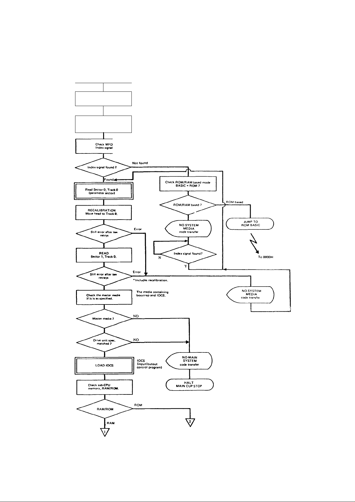
12-1. MAIN CPU IPL FLOW CHART 1/2
MAIN CPU ^
tPL START \
(
Transfer the program
in 1000E-to400E-.
MZ 3500
12. IPL FLOW CHART
, Jump to 400EH
ROM/RAM test Select
memory location
SUM IPL START
Contents of parameter sector
1. Kind of MFD
Single-side double-dencity or double side double
denciiy.
2. Track and sector where IOCS is stored. Loadt tq
and truch
Number of sectors
Note' The sub loader is contained m the leading sector.
/'
I
103
Page 97
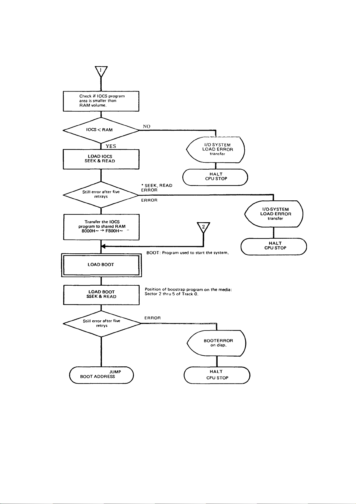
MZ3500
MAIN CPU IPL FLOW CHART 2/2
104
Page 98

12 2. SUB CPU IPL FLOW CHART
MZ-3500
A
Th« mam CPU will perfofm retrials uni t the mjter
media is inserted
- 105 -
Page 99
13-18. PIN CONFIGURATION OF 1C & LSI
MZ-3''O0
Vu 4K A A A') H <A '4
1
LlI U U LJ U LiJ U
nil (111 HR fTl F^ r«J r*J
74 LS 00
lc>J
lA IB IN A H ZN(M
74 LS 02
Vcc 4Y 4B 4A 1Y IB JA
,rsr
ill Lii LiJ Le
lY lA IB 2Y
74 LS
Vet 4B 4A 4Y
rirj n?] FT] m
03
tg?
IJLI LiJ LiJ LiJ LiJ L±J U
Fj F?1 FI FYl fiil |il fij
lA IB lY 2A 2B 2Y CND
74 LS 04
Vcc 6A 6Y 5A 5Y 4A 4Y
1 ill ill LJ
2A 2B CND
3B 3A 3Y
FI rn
74LS125
R R n H |Ti m
IjJ 'liJ LiJ LlI LlI LlJ LiJ
74 LS I 38
DATA <H TPLTS
NLI N 0 Y1 Y’’ Y’^ Y4 Y5 Y6
FTTi 1 T 1
)r
M Yl YZ YJ Y4 Yb
B (. < ZA ( ZB ( 1 Y7
■ J I i r
A H ( A GZb C 1^ Y7 CSU
. . , , . ^
Vet C ¿A ZB 2Y0 2Y1 2Y2 2Y3
fTin^r^n^frriiTiriRrri
C A B YO YI Y2
.................
Ol T
74 LS 139
SELECT DATA OUTPtTS
xnzr
)
A B YO Yl Y2 Y3
■ I I Y Y TV
r
IjJliJlJjljJljJLllLljLLJ
U lA IB. ,IYO lYI 1Y2 JY3. GND
SELECT DATA OUTPUTS
J
GNI)
I> CLOCK CLOCK fTa>
PARALLEL INPITTS
Mx fC lYI 2A4 lYi JAS 1Y3 2A2 IY4 2AI
rararni^rann^iriripFirTri
I ■ I IM hi I ■ I I i I I»I Li I«I I “ I 11 »1
1C lAl 2Y4 lA^ ’Y8 IA3 ■’Y’ IA4 2YI CM
Vcc *G lYl tA4 IY2 2A8 IY8 2A2 IY4 2A1
I i.l I « I 1» I 1« I I i I 1 » I I 7 I I e [ 1 » I 1 loT
1C >A1 2Y4 IA2 2Y3 IAS 2Y2 IA4 2Y1 GND
■ INHIBIT
1RRR
LlI LiJ Lil Ll
lA lY 2A 2Y
74 Li
VLc 4B 4A 4Y
FI FI FI F
LJ LiJ LiJ LlI Lil LlI LlI
FI FI Fi FI F<n |T] r»l
lA IB lY 2A 2B 2Y GND
74 LS 10
Vcc IC lY 3C 3B 3A 3Y
lA IB 2A ZB ZC 2Y CM»
1 LiJLLi LU
08
tel
lA lY CM»
3b 3A lY
W FI
' OlIKT '
74 LS 14
lA lY 2A 2Y 3A 3Y GND
fTTi n?l [itl nil fiTi pri
------------------------------
' OlTiLT
V(.C 6A 6Y 5A SY 4A 4V
ra ra nil nri ra [Ti
LlJ LiJ LiJ Lei LiJ LLl LiJ
Vec STKOBF 4A 4Y 8A SB 8Y
LJLeJ'LDliJLiJLLjLJLiJ
SLJtCl lA IH IN 2A B 2Y (ND
'
------------------
[^riTIFFirrnnTinripTiniiri^nTI
l_i Jli II 3 ih II 5 || 6 II 7 II 8 II 9 |||0|
GND
18
Page 100

о 9 ^
<2§S^Ì53^53S^
П П..П ППП П ПП П ПП ПД
25 ti 3 л s; Q
Pi co vO co fO Pi
s a Й Й Й S Й ем
LQ
<
ЧГ ^n UO
ппппппппппппппппппап
'йЗййй sa^ssassaasM
%
^ ¿J з: 3
'E-
•E
'E
I
,-E
iE
3Î
>
3=
3i
3=
3.3
— емр>ч*1Л«0р-ооо>о — смсо^1Л«х>р-
U U U U'LTU UUUЬЬЬЬЬljQij
= 2!î22i2^, asassasssiEfe
< < < < <
00 o> g
Í
— CMCO'fl'iOtßc^QoaiO —< см СП
UUUUUGUUUÚÚIJUÚÜUULJ U'U'
?|<||g|2|5 5§5¿¿¿¿2¿¿‘
C~L
3'?
г35
■?E
5E
^Зй
3.^
-3ii
'?E
?E
^E
.3s
132
3'2
0)
 Loading...