

Page 1

MZ-700
SERVICE MANUAL
.............................................................
..
SHARP
INDEX
CODE: OOZMZ700SMI/E
PERSONAL COMPUTER
MODEL
MZ-700
MZ-1TOl
MZ-1POl
(FOR THE MZ-lPOI MECHANICAL SECTION
REFER
TO
THE DPG2306 SERVICE MANUAL)
1.
SPECIFICATIONS.
. . . . . . . . . . . . . . . .
..
. . . . .
..
. . . . .
..
. .
..
. .
..
1
2.
NAMES OF
FUNCTIONAL
COMPONENTS. . . . . . . . . . . . . . . . . . .
..
2
3.
SYSTEM BLOCK
DIAGRAM
..............................
_
..
3
4.
SYSTEM
DESCRIPTION.
. . . . . . . . . . . . • . . . . . . . . . . . . .
•.
. . . . .
..
4
5.
DATA
RECORDER
....................................
....
15
6.
COLOUR ENCODER
.......
.
........
. .........
.
............
19
7.
MICRO COLOUR GRAPHIC PRINTER
.........................
20
8.
POWER
SUPPLy
...................
.
.............
•
........
24
9.
IC
SIGNAL
POSITION
.......................•...........
. . 27
10.
CIRCUIT
DIAGRAM
& PARTS
LAyOUT
...•.
..
...
..
....
..
....
29
11.
PARTS GUIDE & LIST
SHARP
CORPORATION
Page 2
~\~Z~
700
1.
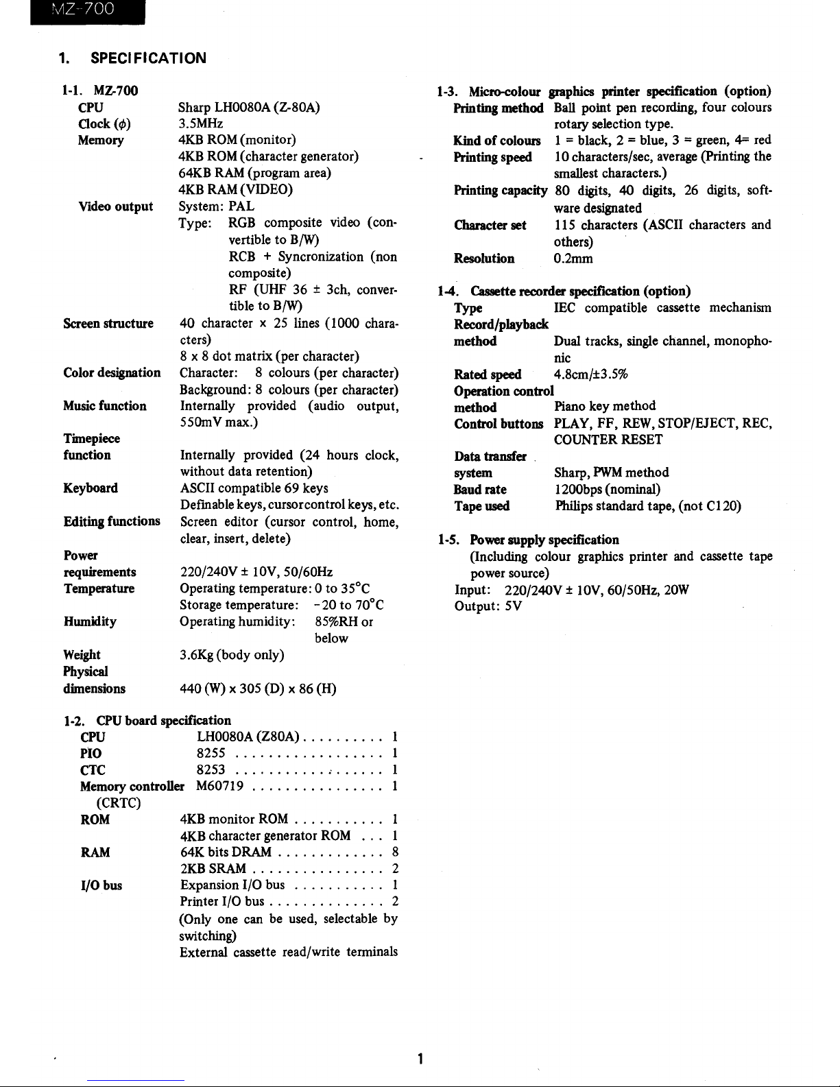
SPECIFICATION
1-1.
MZ-700
CPU
Oock(ct»
Memory
Video
output
Screen structure
Color
designation
Music function
Timepiece
function
Keyboard
Editing functions
Power
requirements
Temperature
Humidity
Weight
Physical
dimensions
Sharp LH0080A (Z-80A)
3.5MHz
4KB
ROM (monitor)
4KB
ROM (character generator)
64KB RAM (program area)
4KB RAM
(VIDEO)
System: PAL
Type: RGB composite video (con-
vertible
to
B/W)
RCB
+ Syncronization
(non
composite)
RF
(UHF
36
± 3ch, conver-
tible
to
B/W)
40
character x 25 lines
(1000
characters)
8
x 8
dot
matrix
(per
character)
Character: 8 colours
(per
character)
Background: 8 colours (per character)
Internally provided (audio
output,
55OmVmax.)
Internally provided
(24
hours clock,
without data retention)
ASCII compatible
69
keys
Defmable keys, cursor control keys, etc.
Screen editor (cursor control, home,
clear, insert, delete)
220/240V ± 10V, SO/60Hz
Operating temperature: 0
to
35°C
Storage temperature:
-20
to
70°C
Operating humidity: 85%RH or
below
3.6Kg
(body
only)
440
(W) x 305 (D) x
86
(H)
1-2.
CPU board specification
CPU
LH0080A (Z80A) . . . . . . . .
..
I
PlO 8255
..................
I
CTC 8253
...................
I
Memory controller M60719
................
I
(CRTC)
ROM
RAM
I/O bus
4KB
monitor
ROM . . . . . . . . .
..
I
4KB character generator
ROM
...
I
64K bits DRAM . . . . . . . . . . .
..
8
2KB
SRAM
................
2
Expansion
I/O bus
...........
I
Printer I/O bus . . . . . . . . . . . .
..
2
(Only one can be used, selectable
by
switching)
External cassette read/write terminals
1-3. Micro-colour graphics printer specification (option)
Printing method Ball point pen recording, four colours
rotary selection type.
Kind
of
colours I = black, 2 = blue, 3 = green, 4= red
Printing speed
10
characters/sec, average (Printing the
smallest characters.)
Printing capacity
80
digits,
40
digits, 26 digits, soft-
ware designated
Character set 115 characters
(ASCII characters and
others)
Resolution
0.2mm
1-4. Cassette recorder specification (option)
Type
IEC compatible cassette mechanism
Record/playback
method
Dual tracks, single channel, monopho-
nic
Rated speed 4.8cm/±3.5%
Operation control
method Piano key
method
Control
buttons
PLAY,
FF,
REW, STOP/EJECT, REC,
COUNTER RESET
Data transfer .
system
Baud rate
Tape
used
Sharp,
PWM
method
1200bps (nominal)
Philips standard tape,
(not
C120)
1-5.
Power supply specification
(Including colour graphics printer and cassette tape
power source)
Input:
220/24OV ± 10V, 60/50Hz, 20W
Output:
5V
Page 3

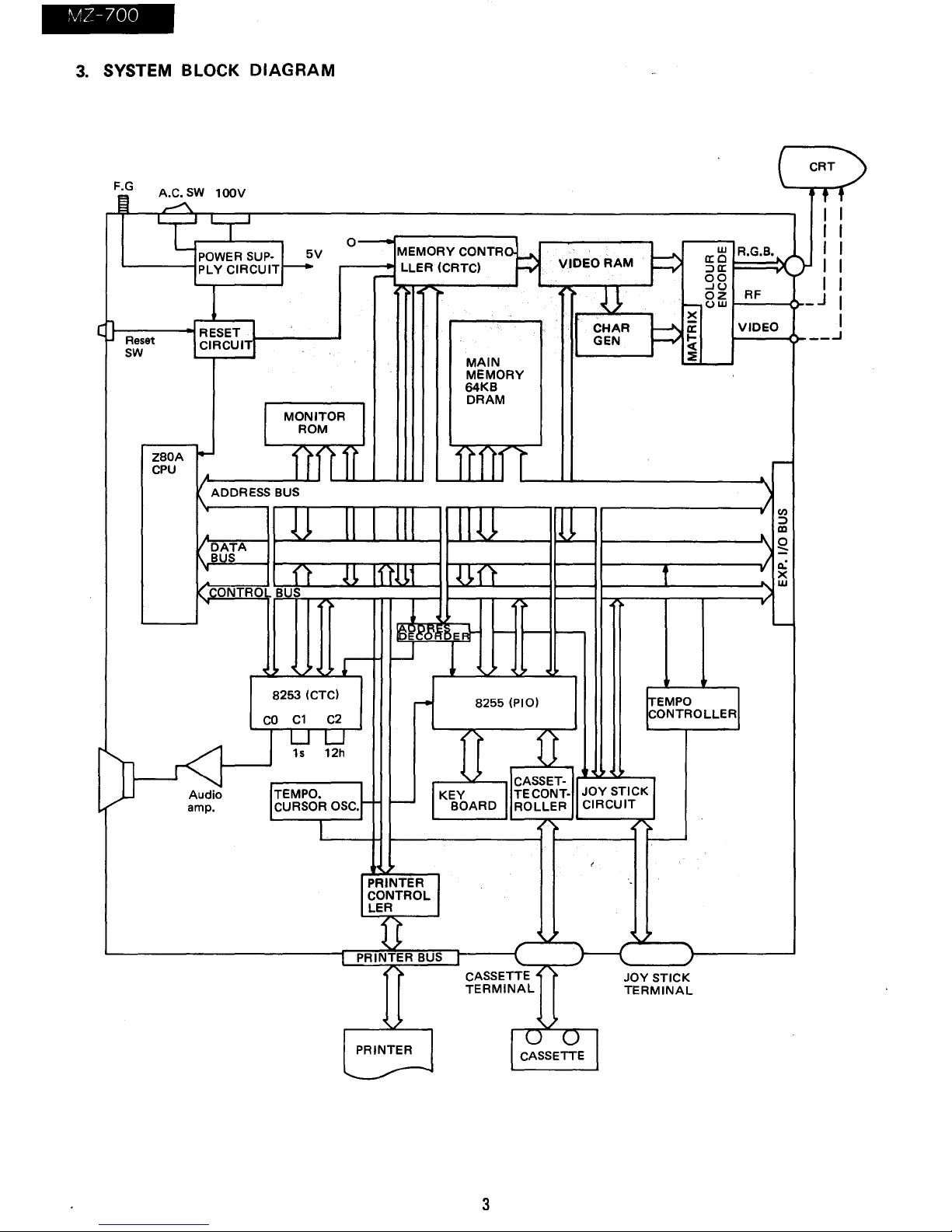
2.
NAME
OF
FUNCTIONAL
COMPONENT
MZ-700 Front view
Main
kev
board
-----'
MZ-700
Aeer
view
Channel switch
RF
terminal
BrN-Colour
switch
Composi!
terminal
Dat8 recorder
!c3S$IIttll)
AGe
terminal
CantUI!
re<:order
jKk
EKt.
output
terminal
Joy
nick
ulfminal
1
plOHtr
printer
Ext.
printer
terminal
MZ-700
plolter
prioter
recorder (cassette)
INS.
DEL
key
":::d'---,----CUrSOI
control
keV$
.
socket
Reset switch
Volume
Adiust
F,.me
ground
termmal
Page 4
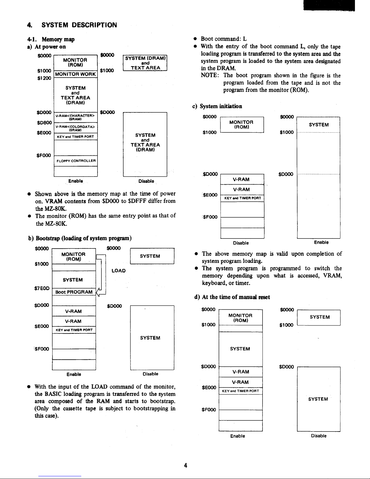
~"q-700
3. SYSTEM BLOCK DIAGRAM
(
CRT
F.G
A.C.
sw
100V
I~
-""
t t
~PO~UP'
!II
0-
5V
MEMORY CONTRa.
Fi
p
w
R.G.B. I I
PLY CIRCUIT
llER
(CRTC)
VIDEO
RAM
a::
Cl
-..,
I I
,.--
:Ja::
00
RF I I
~
~~
...JU
oz
-uw
_J
I
eJ
Reset
RESET 1
~
~
I
CHAR
a::
VIDEO
CIRCUITJ
I GEN
....
...J
sw
c(
MAIN
~
MEMORY
64KB
DRAM
MONITOR
ROM
Z80A
i-
III
IT
CPU
A
,......
\ ADDRESS
BUS
\
I
n
I
n=
-y
en
:J
A
"
III
~dJA
\
Q.
I
-
"
ft
H
rn.
t\.0
-
t
"
a:
..
X
(ONTROl
BUS
I--
.
w
...-
>
I--
...
~I
?8m
ER!-
f--
I--
I--
'--
r
f--
~
t
!.
8253 (CTC)
r-
8255 (PlO)
EMPO
CO
C1
C2
CONTROLLER
t,;J~
"
>
0(
CASSET·
Audio
TEMPO. +
f..--
KEY I
TECONT·
11
JOY STICK 1
amp.
CURSOR
OSC.
BOARD
ROLLER
CIRCUIT
I
~
I--
t
PRINTER
CONTROL
LER
~
r "\
PRINTER BUS
J
CASSETTE
JOY STICK
TERMINAL
TERMINAL
~
U U I
CASSETTE
3
Page 5
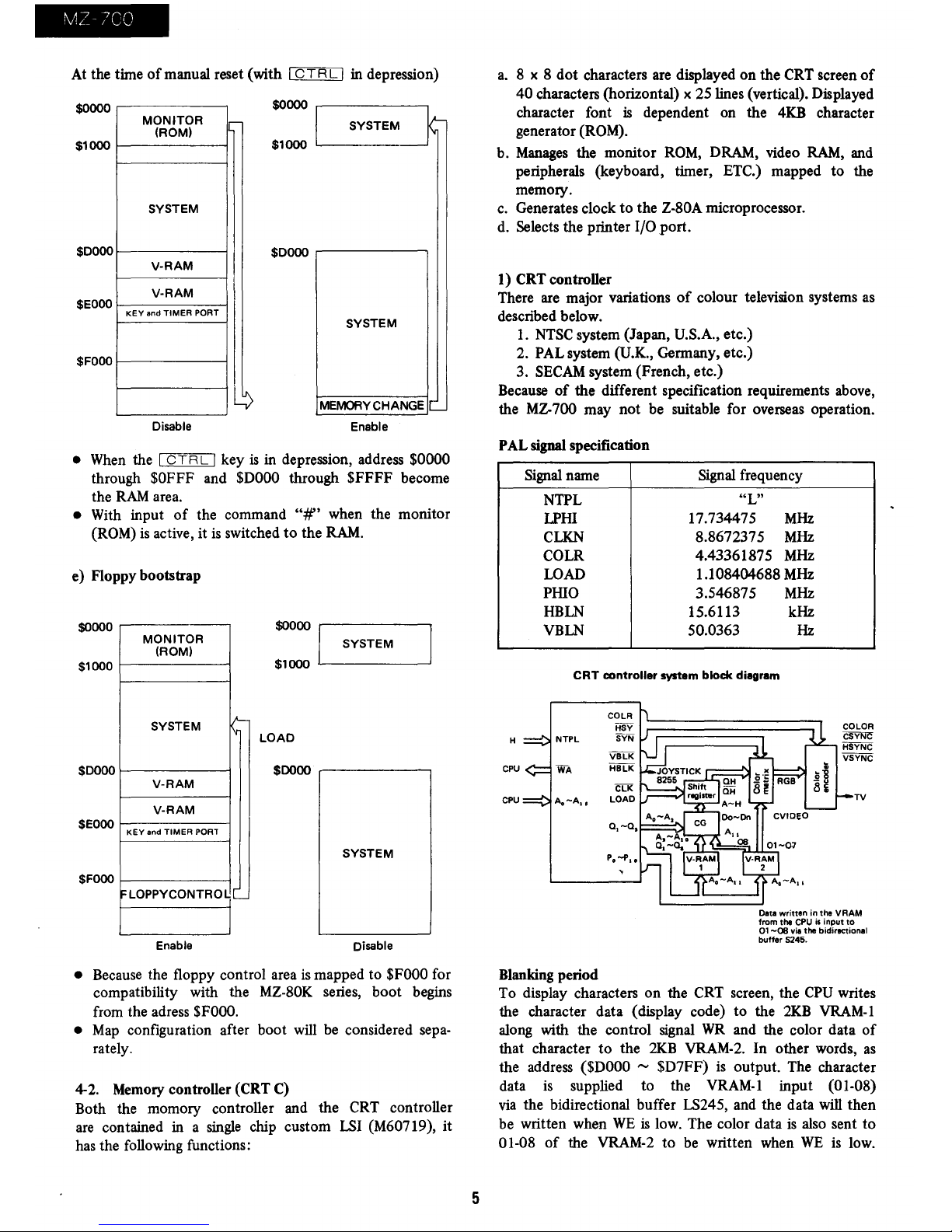
4.
SYSTEM
DESCRIPTION
4-1.
Memory map
a) At power
on
$0000
$1000
$1200
$0000
$0800
$EOoo
$FOoo
MONITOR
(ROM)
MONITOR WORK
SYSTEM
and
TEXT
AREA
(DRAM)
V·RAM<CHARACTER>
(SRAMI
V·RAM<COLORDATA>
(SRAMI
KEY
and
TIMER
PORT
FLOPPY CONTROLLER
Enable
$0000
$1000
$0000
SYSTEM
(DRAM)
and
TEXT
AREA
SYSTEM
and
TEXT
AREA
(DRAM)
Disable
• Shown above
is
the memory map at the time
of
power
on.
VRAM
contents from$DOOO to $DFFF differ from
the
MZ·80K.
• The monitor (ROM) has the same entry point
as
that
of
the MZ·80K.
b) Bootstrap (loading
of
system program)
$0000 $0000
MONITOR
Ir--
(ROfv\)
1'-
SYSTEM
$1000
LOAD
SYSTEM
$7EOD
Boot PROGRAM
~
'11
$0000
$0000
V·RAM
V·RAM
$EOoo
KEY and
TIMER
PORT
SYSTEM
Eneble
Disable
• With the input
of
the LOAD command
of
the monitor,
the
BASIC
loading program
is
transferred
to
the system
area composed
of
the
RAM
and starts
to
bootstrap.
(Only the cassette tape
is
subject
to
bootstrapping in
this case).
4
• Boot command: L
• With the entry
of
the boot command
L,
only the tape
loading program
is
transferred
to
the system area and the
system program
is
loaded
to
the system area designated
in the DRAM.
NOTE: The boot program shown in the figure
is
the
program loaded from the tape and
is
not the
program from the monitor
(ROM).
c) System initiation
$0000
$1000
MONITOR
(ROM)
.$0000
,-------,
V·RAM
V·RAM
$Eooo I--KE-Y-ond-TI-M-ER-P-OR-T-l
:$Fooo
1--------1
Disable
$0000
,-----,
SYSTEM
$1000 ----------------------
$0000
---------------------------
Enable
• The above memory map is valid upon completion
of
system program loading.
• The system program
is
programmed
to
switch the
memory depending upon what
is
accessed,
VRAM,
keyboard, or timer.
d) At
the
time
of
manual reset
$0000
$1000
MONITOR
(ROM)
$0000 I SYSTEM
$1000
~-----~
SYSTEM
$0000
$0000
,-------,
V·RAM
V-RAM
$EOoo
KEY
and
TIMER
PORT
SYSTEM
$FOoo
Enable
Disable
Page 6
~1Z
-7CO
At the time
of
manual reset (with I
CTRL
I in depression)
$0000
$0000
SYSTEM
~
MONITOR
-
(ROM)
$1000
$1000
SYSTEM
$0000
$0000
V-RAM
V-RAM
$EOoo
KEY
and
TIMER
PORT
SYSTEM
$FOOO
~
MEMORY CHANGE
'--
Disable
Enable
•
When
the I C T R L I key
is
in depression, address $0000
through $OFFF and
$DOOO
through $FFFF become
the
RAM
area.
• With input
of
the command ":If' when the monitor
(ROM)
is
active, it
is
switched
to
the
RAM.
e) Floppy bootstrap
$0000
....--------,
MONITOR
(ROM)
$1000
f----------I
SYSTEM
iI-
Iv
$DOOO~----~
V-RAM
V-RAM
$EOoo
i-
K-E
-
y
-an-d T-IM-E-R-PO-R-l
-I
$FOoo
f----------I
FLOPPYCONTRO~L-
Enable
$0000 I
SYSTEM
$1000
~----~
LOAD
$0000
,------,
SYSTEM
Disable
• Because the floppy control area
is
mapped to
$FOOO
for
compatibility with the
MZ-80K series, boot begins
from the adress
$FOOO.
•
Map
configuration after boot will
be
considered sepa-
rately.
4-2. Memory controller
(CRT
C)
Both the momory controller and the CRT controller
are
contained in a
single
chip custom
LSI
(M60719), it
has the following functions:
5
a.
8 x 8 dot characters are displayed on the CRT screen
of
40
characters (horizontal) x 25 lines (vertical). Displayed
character font
is
dependent on the
4KB
character
generator (ROM).
b.
Manages
the monitor
ROM,
DRAM, video
RAM,
and
peripherals (keyboard, timer,
ETC.) mapped to the
memory.
c.
Generates clock to the Z-80A microprocessor.
d.
Selects the printer I/O port.
1)
CRT controller
There are major variations
of
colour television systems
as
described below.
1.
NTSC
system (Japan, U.S.A., etc.)
2.
PAL system (U.K., Germany, etc.)
3.
SECAM
system (French, etc.)
Because
of
the different specification requirements above,
the
MZ-
700 may not be suitable for overseas operation.
PAL signal specification
Signal name
Signal frequency
NTPL
"L"
LPHI 17.734475
MHz
CLKN
8.8672375
MHz
COLR
4.43361875
MHz
WAD
1.108404688
MHz
PHIO 3.546875
MHz
HBLN
15.6113
kHz
VBLN 50.0363
Hz
CRT
controller
system
block
diagram
H
NTPL
CPU
WA
CPU
Blanking period
COLR
HSY
SYN
VBLK
HBLK
CLK
LOAD
TV
Oata written in
the
VAAM
from
the
CPU
is
input
to
01-08
via
the
bidirectional
buffer
5245.
To display characters on the CRT screen, the
CPU
writes
the character data ( display code) to the
2KB
VRAM-l
along with the control signal
WR
and the color data
of
that character
to
the
2KB
VRAM-
2.
In other words,
as
the address
($DOOO
,..,
$D7FF)
is
output. The character
data
is
supplied to the VRAM-l input (01-08)
via
the bidirectional buffer LS245, and the data will then
be written when
WE
is
low. The color data
is
also sent to
01-08
of
the
VRAM-2
to be written when
WE
is
low.
Page 7
To read the contents
of a VRAM
character, the
CPU
sends
out
the relevant address. When
RD
is forced low, the
data
is
then read
via
the bidirectional buffer LS245.
However, the address range
$0000
through $DFFF must
be addressed in order to access
all
the
VRAM.
This address
change
is
carried
out
inside the custom
LSI
with the OUT
command described later.
Accessing
of
the
VRAM
is carried
out
within the blinking
period (BLNK
= "H").
If
BLNK =
"L",
then
WAIT
is
applied to the
CPU
(WA
= "L").
The blanking period discussed here
is
the period that
BLNK
is
in high level.
High
period
of
the BLNK signal
is
so
designed that it
is
shorter than the low period
of
HBLK (horizontal blanking
period).
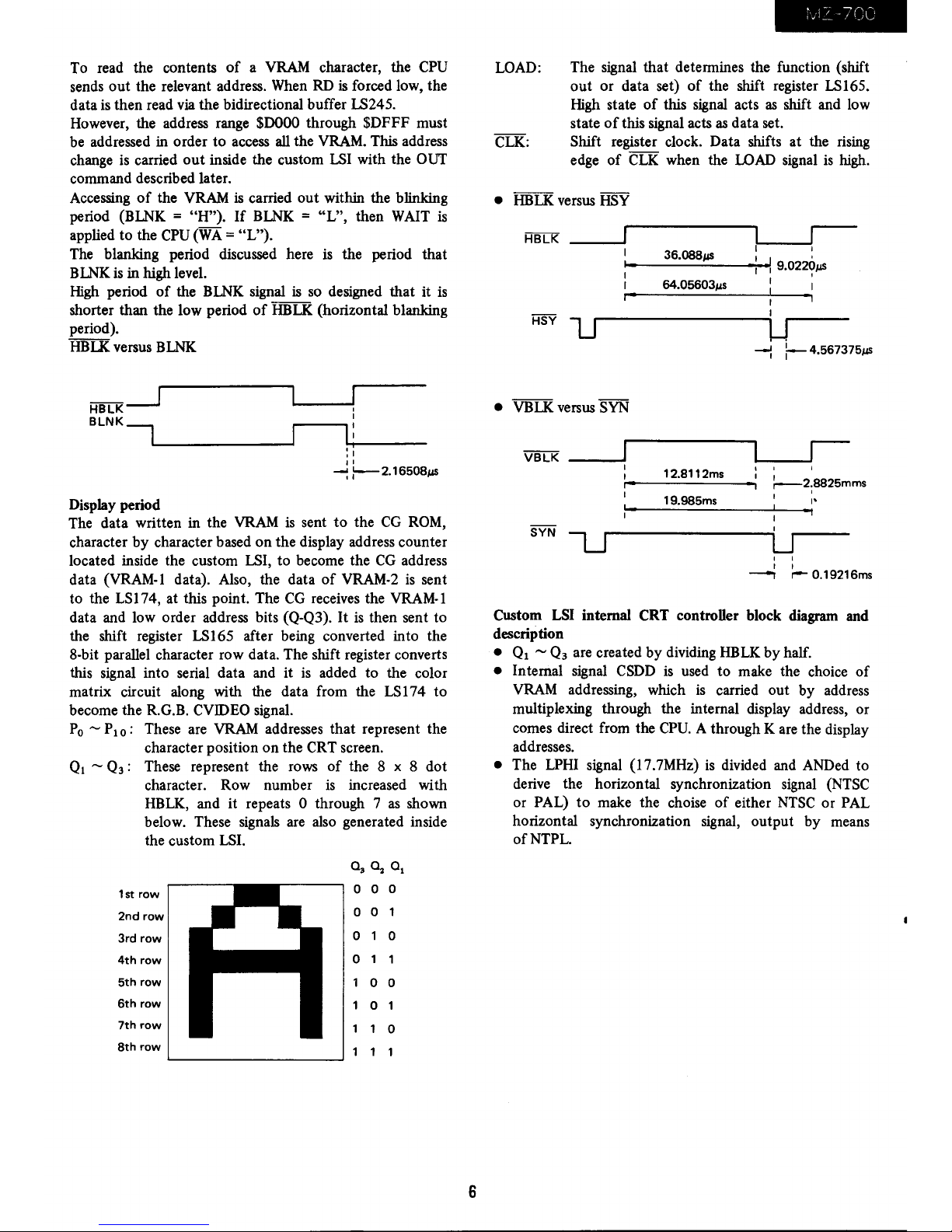
HBLK
versus
BLNK
HBLK~
,
BLNK--,L.
____________
~--~I
!
~
I:
L"I----
, 1
I'
-:
l--
2.165081-1S
Display period
The data written in the
VRAM
is
sent
to
the
CG
ROM,
character
by
character based on the display address counter
located inside the custom LSI, to become the
CG
address
data (VRAM-l data). Also, the data
of
VRAM-2
is
sent
to the LS174, at this point. The
CG
receives the VRAM-l
data and low order address bits (Q-Q3).
It
is
then sent to
the shift register LS165 after being converted into the
8-bit parallel character row data. The shift register converts
this signal into serial data and it
is
added to the color
matrix circuit along with the data from the LS174 to
become the R.G.B.
CVIDEO signal.
Po
- PlO: These are
VRAM
addresses
that
represent the
character position
on
the CRT screen.
Ql
- Q3: These represent the rows
of
the 8 x 8 dot
character. Row number
is
increased with
HBLK,
and it repeats 0 through 7
as
shown
below. These signals are also generated inside
the custom
LS!.
as
a2 a
1
1st row
0 0
0
2nd
row
0 0
1
3rd row
0
0
4th
row
0
1
1
5th
row
1
0 0
6th
row
1
0 1
7th
row
1
1
0
8th
row
1 1
1
6
LOAD:
CLK:
The signal that determines the function (shift
out
or data set)
of
the shift register LS165.
High state
of
this
signal
acts
as
shift and low
state
of
this signal acts
as
data set.
Shift register clock. Data shifts at the rising
edge
of
CLK
when the
LOAD
signal
is
high.
•
HBLK
versus
HSY
!------Jr---
I 1
36.0881-1S
1 1 '
1-1
-----:...----;I-!'j
9.02201-1S
I I '
1
64.05603/015
1
I·
I
I
1J
W.
-l
:--
4.567375j.1S
• VBLK versus
SYN
VBLK
____
~
~
__
~r---
: 12.8112ms
:;
I
r-I--------·~I
r--2;8825mms
1
~_~1~9=.98==5m~s~
__
~_~.:.
u
, 1
1 1
--,
r--
0.19216ms
Custom
LSI
internal CRT controUer block diagram and
description
• Ql -
Q3
are created by dividing
HBLK
by half.
• Internal signal
CSDD
is
used to make the choice
of
VRAM
addressing, which
is
carried out by address
muitiplexing through the internal display address, or
comes direct from the
CPU.
A through K are the display
addresses.
• The
LPHI
signal (l7.7MHz)
is
divided and ANDed to
derive the horizontal synchronization signal
(NTSC
or PAL)
to
make the choise
of
either
NTSC
or PAL
horizontal synchronization signal, output by means
ofNTPL.
Page 8
\
,'1Z
-700
2) Memory controller
In the
MZ·
700, it needs
to
segregate the memory in order
to acheive the above mentioned memory mapping. The
memory controller
is
therefore used
to
perform address
management
of
peripherals assigned
to
the memory such
as
DRAM, monitor
ROM,
video
RAM,
and keyboard. The
bank select method
is
used to switch memory. Memory
selection
is
acheived using the OUT command.
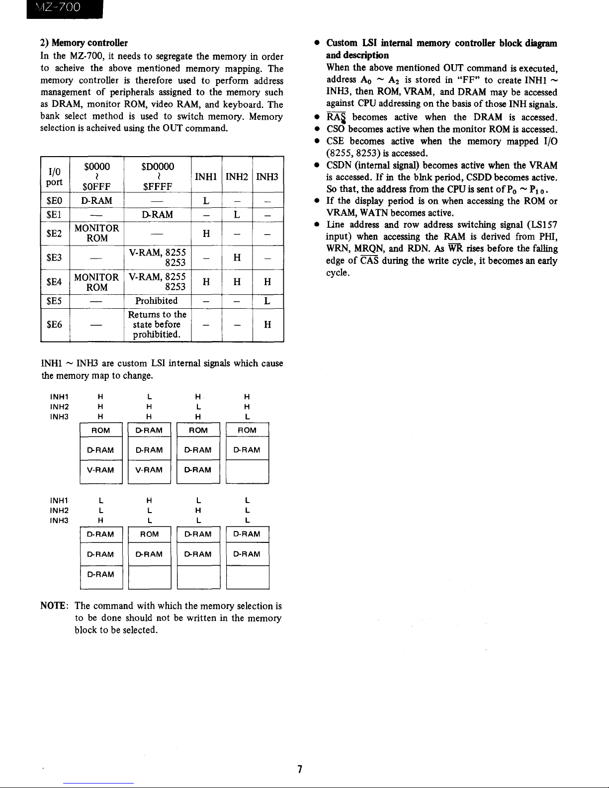
I/O
$0000
$DOOOO
~
l
INHl INH2 INH3
port
$OFFF
$FFFF
$EO
D·RAM
-
L
-
-
$El
-
D-RAM
-
L -
$E2
MONITOR
H
ROM
-
-
-
$E3
-
V·RAM,8255
-
H
-
8253
$E4
MONITOR
V·RAM,8255
H H H
ROM
8253
$E5
-
Prohibited
- -
L
Returns
to
the
$E6
-
state before
-
-
H
prohibitied.
INHl
-
INH3
are custom
LSI
internal signals which cause
the memory map to change.
INH1
INH2
INH3
INH1
INH2
INH3
H L H H
H H L H
H H H L
I--D-_R:_:_M---I
1--:-.:-:-:---1
I---D-_:_OA_MM----j
I
:::
I
V·RAM V·RAM
D-RAM
L
L
H
D·RAM
D-RAM
D·RAM
H
L
L
ROM
D-RAM
L
H
L
D-RAM
D-RAM
L
L
L
D-RAM
D·RAM
NOTE: The command with which the memory selection
is
to
be
done should not
be
written in the memory
block to be selected.
7
• Custom LSI internal memory controller block diagram
and description
When the above mentioned
OUT command
is
executed,
address
Ao
,..,
A2
is stored in
"FF"
to
create INHl
,..,
INH3,
then
ROM,
VRAM, and
DRAM
may be accessed
against
CPU addressing
on
the basis
of
those INH signals.
•
RA~
becomes active when the DRAM
is
accessed.
•
CSO
becomes active when the monitor
ROM
is accessed.
•
CSE
becomes active when the memory mapped I/O
(8255,8253)
is accessed.
• CSDN (internal signal) becomes active when the VRAM
is
accessed.
If
in the blnk period, CSDD becomes active.
So
that, the address from the CPU
is
sent
of
Po
,..,
PlO.
•
If
the display period is
on
when accessing the
ROM
or
VRAM, W ATN becomes active.
•
line
address and row address switching signal (LS157
input) when accessing the
RAM
is derived from PHI,
WRN,
MRQN, and RDN.
As
WR
rises before the falling
edge
of
CAS
during the write cycle,
it
becomes an early
cycle.
Page 9
IV?
7ce
4-4. Memory controller (CRTC) circuit description
The memory controller and
the
CRTC are contained in
the
single chip custom LSI (M60719).
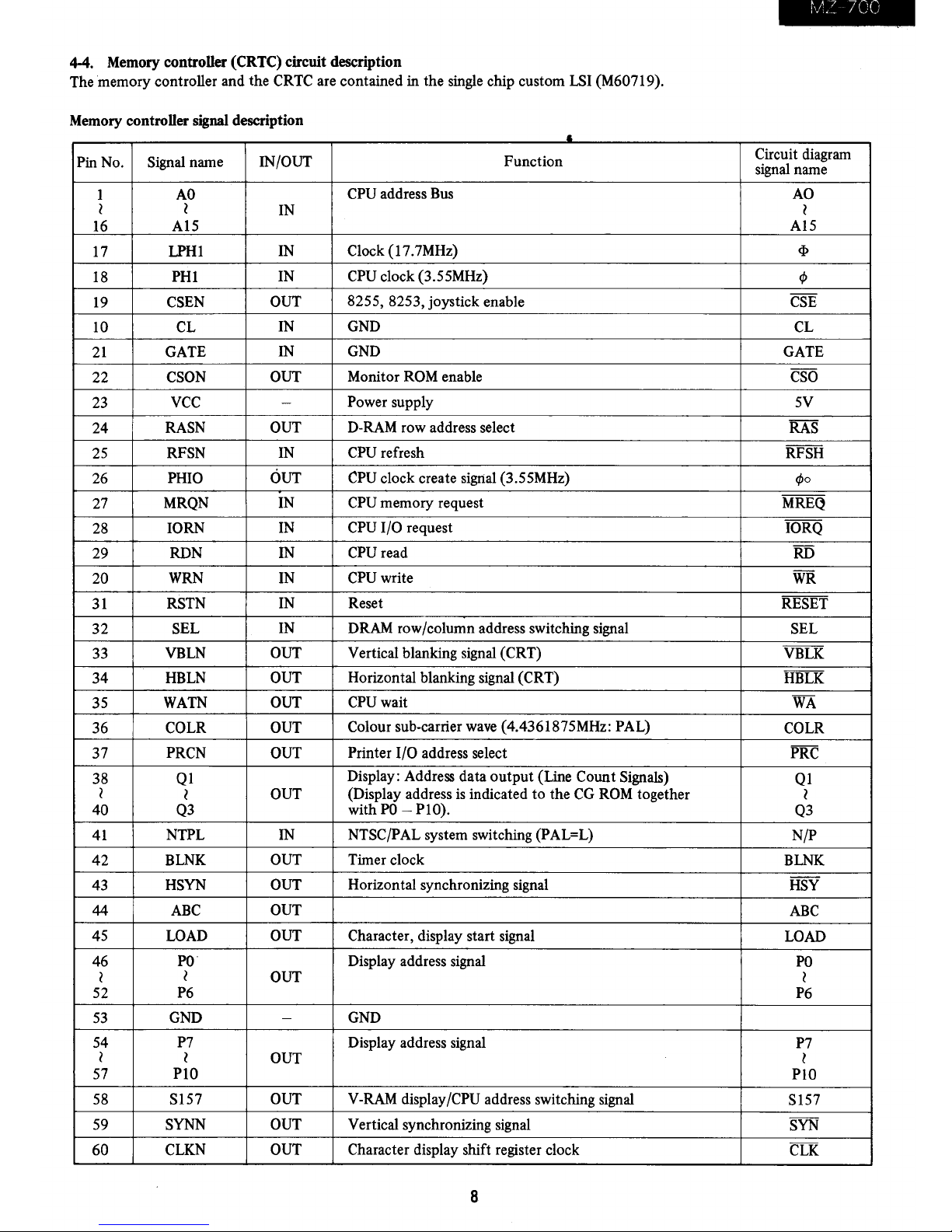
Memory controller signal description
&
Pin No.
Signal name IN/OUT
Function
Circuit diagram
signal name
1
AO
CPU address Bus
AO
l
l
IN
l
16
A15
A15
17
LPH1
IN
Clock (17.7MHz)
<I>
18
PHI
IN CPU clock (3.55MHz)
cp
19
CSEN
OUT
8255, 8253, joystick enable
CSE
10 CL
IN GND
CL
21
GATE
IN GND
GATE
22
CSON OUT
Monitor ROM enable
CSO
23
VCC
-
Power supply
5V
24
RASN
OUT
D-RAM row address select
RAS
25
RFSN IN
CPU refresh
RFSH
26
PHIO
OUT
CPU
clock create signal (3.55MHz)
cpo
27
MRQN
IN
CPU memory request MREQ
28
10RN
IN CPU I/O request IORQ
29
RDN IN
CPU read
RD
20
WRN IN
CPU write
WR
31
RSTN
IN Reset
RESET
32
SEL
IN DRAM row/column address switching signal
SEL
33
VBLN
OUT
Vertical blanking signal (CRT)
VBLK
34
HBLN
OUT Horizontal blanking signal (CRT)
HBLK
35 WATN
OUT
CPU
wait
WA
36
COLR
OUT
Colour
sub-carrier wave (4,4361 875MHz: PAL)
COLR
37
PRCN OUT Printer I/O address select
PRC
38
Q1
Display: Address data
output
(Line
Count
Signals)
Ql
l
l
OUT (Display address
is
indicated
to
the
CG ROM together
l
40
Q3
with
PO
- PlO).
Q3
41
NTPL IN NTSC/PAL system switching (PAL=L)
N/P
42
BLNK
OUT Timer clock
BLNK
43
HSYN OUT
Horizontal synchronizing signal
HSY
44
ABC
OUT
ABC
45
LOAD
OUT
Character,
display start signal
LOAD
46
PO
Display address signal
PO
l
~
OUT
l
52
P6
P6
53
GND
-
GND
54
P7 Display address signal
P7
l
l
OUT l
57
PlO
PlO
58
S157 OUT V-RAM display/CPU address switching signal
S157
59
SYNN OUT Vertical synchronizing signal
SYN
60
CLKN
OUT Character
display shift register clock
CLK
8
Page 10
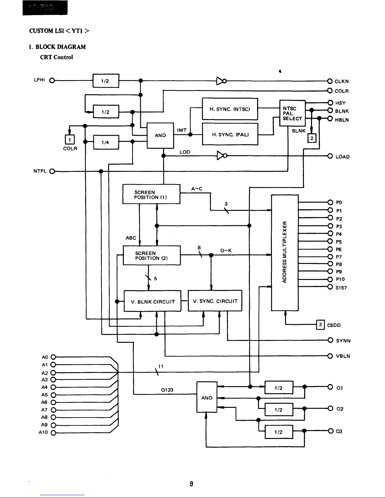
CUSTOM
LSI
< YTl >
1.
BLOCK
DIAGRAM
CRT
Control
LPHI
0
J
I
l-{
NTPL
AO
A1
A2
A3
A4
A5
A6
A7
A8
A9
A10
0
0
('
-
9
0
0
0
0
0
0
0
Eh
H
COLR
1/2
1/2
1/4
"
/
/
/
/
/
/
/
I
J
I--
IMT
I
I.....-
AND
LOO
SCREEN
POSITION (1)
ABC
r--
SCREEN
POSITION (2)
"
I'
5
~
V.
BLNK
CIRCUIT
~
•
L---
\
11
,
0123
-
~
r--
H. SYNC. (NTSC)
r--
H. SYNC. (PAL)
f----
-
...,
A-C
3
\.
,
8
D-K
\
,
~
V. SYNC.
CIRCUIT
I
1
1/2
AND
It
I
1/2
-
Y
1/2
9
NTSC
PAL
SELECT
BLNK0
~
a:
w
X
w
..J
0..
i=
..J
::>
::i:
Cl)
Cl)
w
a:
0
0
et
f
I
-
f
I
-
I
1
r
~
-
~
~
"V
~
~
~
"U
~
~
~
~
Y
V
~
"!
"0
CLKN
COLR
HSY
BLNK
HBLN
LOAD
PO
P1
P2
P3
P4
P5
P6
P7
P8
pg
P10
S157
3
CS
DD
SYNN
-0
VBLN
"0
01
02
Q
03
Page 11
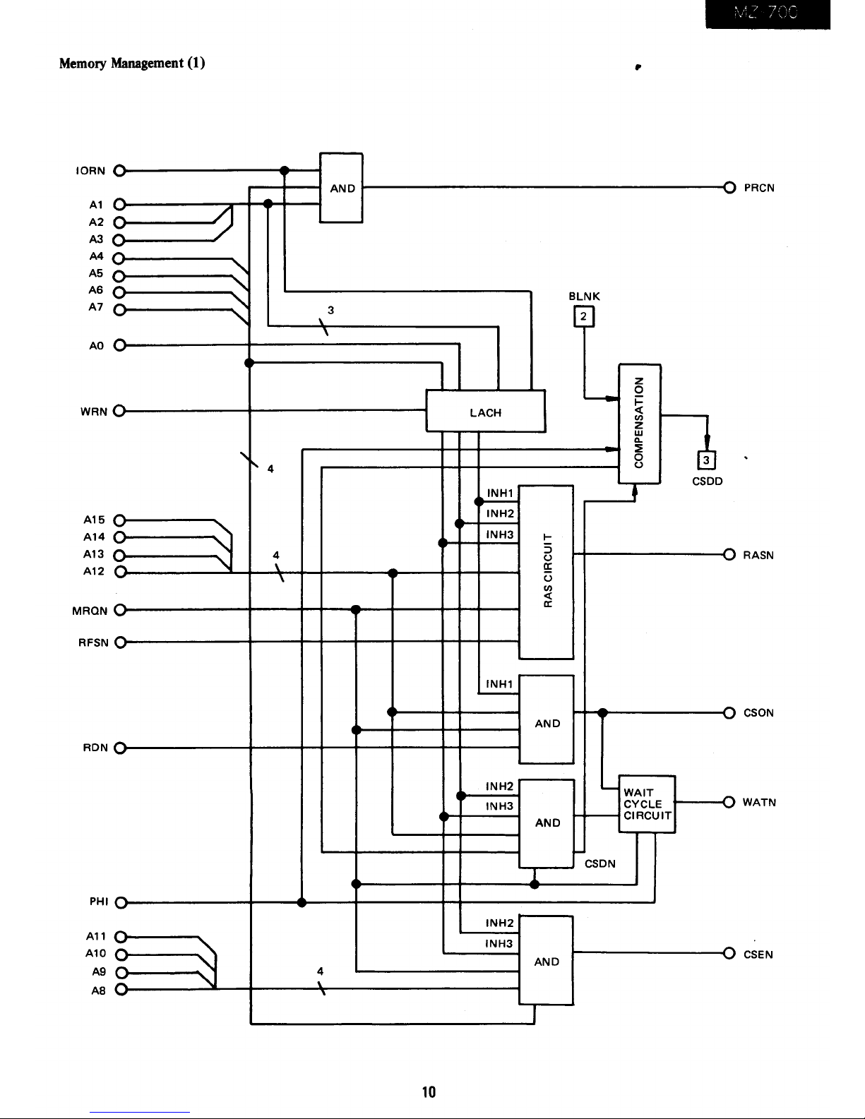
Memory
Management
(1)
IORN
A1
A2
A3
A4
A5
AS
A7
AO
WRN
A15
A14
A13
A12
MRQN
RFSN
RDN
PHI
A11
A10
A9
AB
,...
"
0
~
0
0
0
."
0
"
0
-"
.....
"
"
0
0
'"
0
0
"
"
0
'\
-
0
0
0
0
-
:::.
~
~
'-
0
AND
3
\.
,
r--
4
4
\
,
4
\.
•
-0
PRCN
BLNK
2
Z
'----
0
~
LACH
<C
(f.I
~
Z
w
a..
~
0
U
INH1
•
CSDD
INH2
INH3
I-
:;
u
RASN
!!:
U
(/)
<C
a:
INH1
')
'"
CSON
AND
INH2
-
WAIT
-0
INH3
CYCLE
WATN
AND
CIRCUIT
CSDN
1
INH2
INH3
AND
CSEN
10
Page 12
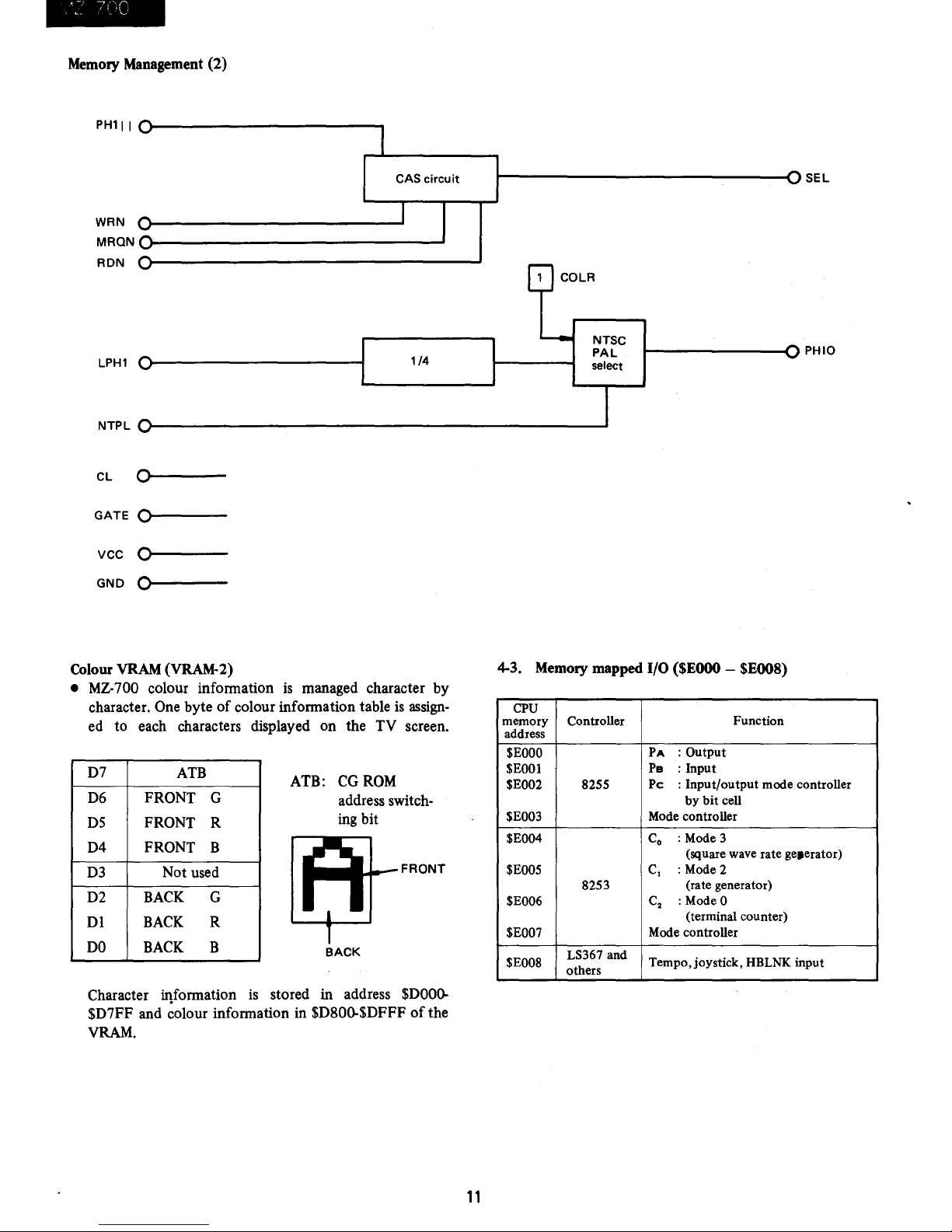
Memory Management
(2)
PH111
WRN
MRQN
RDN
LPH1
NTPL
CL
GATE
VCC
GND
0
0
0
0
Colour VRAM (VRAM-2)
CAS
circuit
1/4
•
MZ-
700 colour infonnation
is
managed character by
character. One byte
of
colour infonnation table is assign-
ed
to
each characters displayed on the
TV
screen.
D7
D6
D5
D4
D3
D2
D1
DO
ATB
FRONT G
FRONT R
FRONT
B
Not used
BACK
G
BACK R
BACK
B
ATB: CGROM
address switchingbit
....
+-_FRONT
BACK
Character iqfonnation
is
stored in address
$DOOQ.
$D7FF and colour infonnation in $D80Q.$DFFF
of
the
VRAM.
11
~------------------------------<1SEL
COLR
NTSC
PAL
select
~-------------In
PH
10
4-3. Memory
mapped
I/O
($EOOO -$EOO8)
CPU
memory Controller
Function
address
$EOOO
PA
: Output
$EOOl
Pe : Input
$E002
8255
Pc
: Input/output mode controller
by bit cell
$E003 Mode controller
$E004
Co
: Mode 3
(square wave rate ge»erator)
$E005
C,
: Mode 2
8253
(rate generator)
$E006
C
2
: Mode 0
(terminal counter)
$E007
Mode controller
$E008
LS367 and
Tempo,joystick,
HBLNK input
others
Page 13
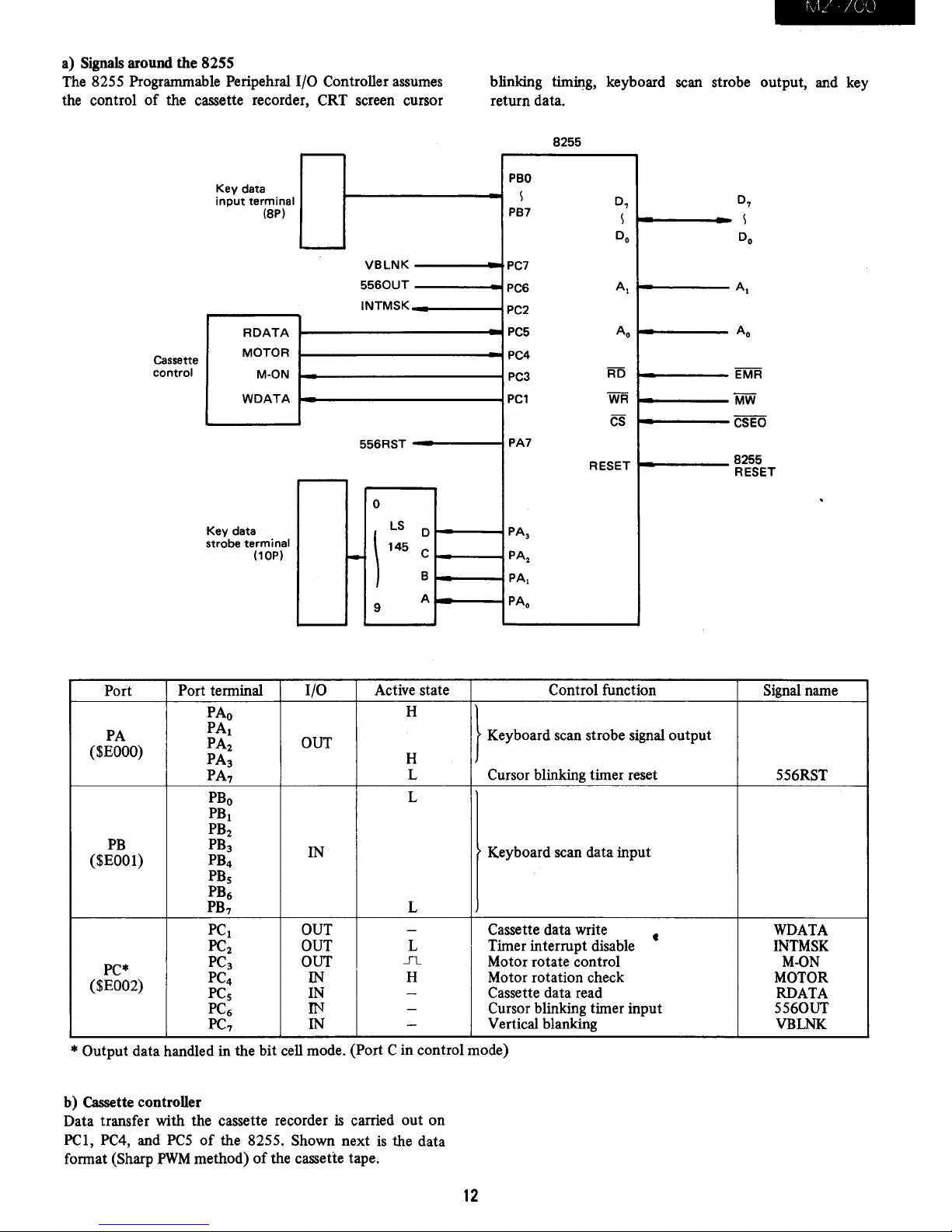
a) Signals around
the
8255
The 8255 Programmable Peripehral I/O Controller assumes
the control
of
the cassette recorder, CRT screen cursor
Port
PA
($EOOO)
PB
($EOOl)
PC·
($EOO2)
Cassette
control
Key data
input
terminal
(8P)
RDATA
MOTOR
M·ON
WDATA
Key data
strobe terminal
(lOP)
Port terminal
PA
o
PAl
PA
2
PA
3
PA
7
PB
o
PB
I
PB
2
PB
3
PB
4
PB
s
PB
6
PB
7
PC
I
PC
2
PC
3
PC
4
PC
s
PC
6
PC
7
r---
'-
VBLNK
5560UT
INTMSK
556RST
0
LS
0
\
145
-
C
B
9
A
I/O
Active state
H
OUT
H
L
L
IN
L
OUT
-
OUT
L
OUT
51..
IN
H
IN
-
IN
-
IN
-
blinking timing, keyboard scan strobe output, and key
return data.
8255
PBO
\
0,
PB7
\
Do
PC7
PC6
AI
PC2
PC5
Ao
PC4
PC3
RD
PCl WR
CS
PA7
RESET
PA,
PA.
PAl
PA
o
Control function
}
Keyboud
scan stwhe slgnal output
Cursor blinking timer reset
Keyboard scan data input
Cassette data write
•
Timer interrupt disable
Motor rotate control
Motor rotation check
Cassette data read
Cursor blinking timer input
Vertical blanking
0,
AI
8255
RESET
Signal name
556RST
WDATA
INTMSK
M-ON
MOTOR
RDATA
5560UT
VBLNK
•
Output
data handled in the
bit
cell mode. (Port C in control mode)
b)
Cassette controller
Data transfer with the cassette recorder is carried
out
on
PCI, PC4, and
PC5
of
the 8255. Shown next
is
the data
format (Sharp
PWM
method)
of
the cassette tape.
12
Page 14
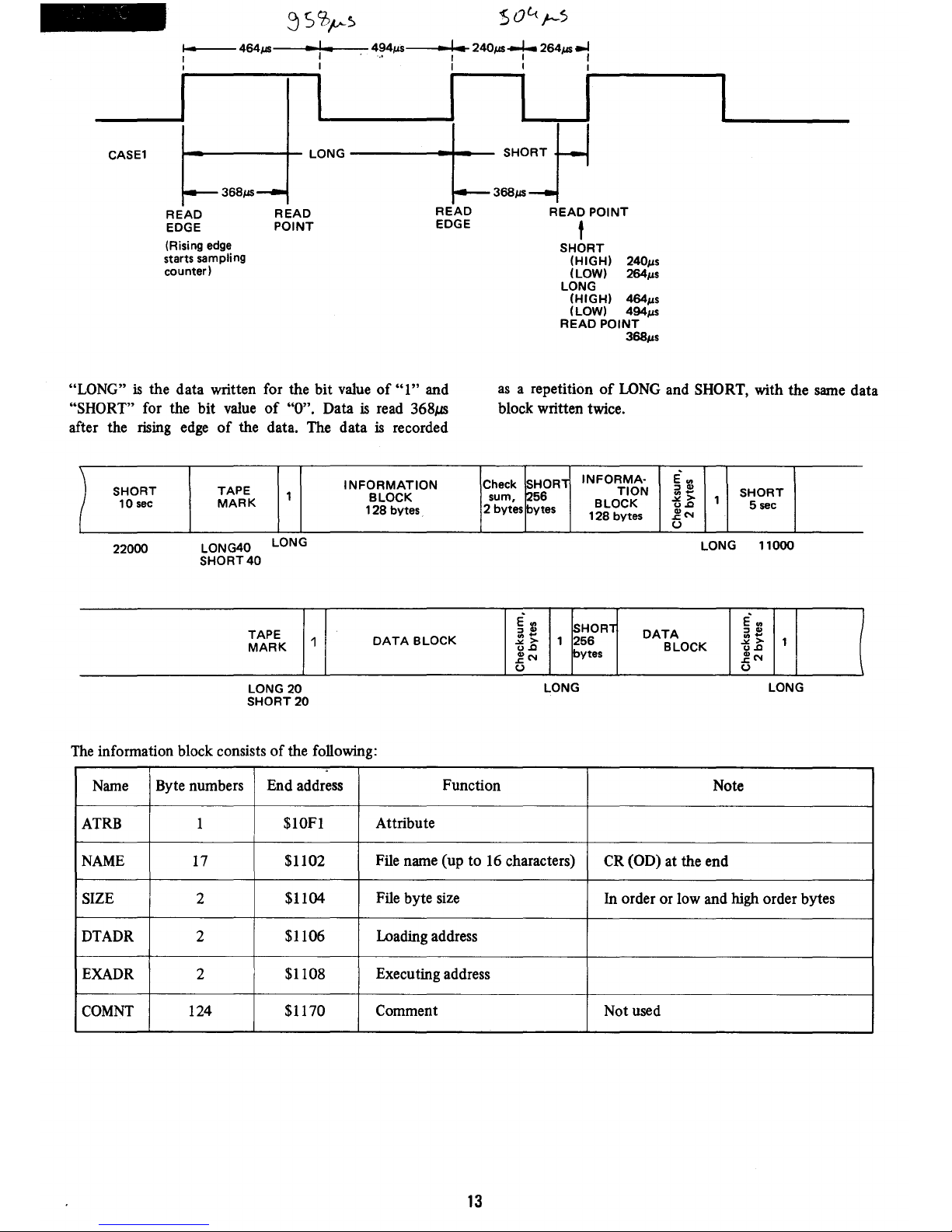
1-o1
..
_--464~-
__
...
II.oo
...
_-49
.•
4j.1S----I
..
-+oI
.....
240~-'-
264~'"
, I
"I
I I I ,
;.'
______
_
I
CASE1 LONG
-----
....
--
SHORT
U
368j.1S 368j.1S
--J
'
READ
READ READ
READ
POINT
EDGE
POINT
EDGE t
(Rising
edge
SHORT
starts sampling
(HIGH)
240lls
counter) (LOW) 264lls
LONG
(HIGH)
464lls
(LOW)
494j.1S
READ
POINT
368lls
"LONG"
is
the data written for the bit value
of"
1" and
"SHORT" for the bit value
of
"0".
Data is read
368~
after the rising edge
of
the data. The data is recorded
as
a repetition
of
LONG and SHORT, with the same data
block written twice.
I
SHORT
10
sec
22000
TAPE
1
MARK
LONG40
SHORT40
LONG
TAPE
MARK
LONG
20
SHORT
20
INFORMATION
BLOCK
128
bytes.
1
DATA
BLOCK
Check
!SHORT
INFORMA·
E
..
TION
:;,a>
SHORT
sum,
~56
.....
BLOCK
~>
1
2 bytes
~ytes
u.rJ
5
sec
128
bytes
1!N
u
LONG
11000
E
Xl
isHORT
E"
..
as:
DATA
:;,a>
.....
~.rJ
1 256
BLOCK
~>
1
Ibytes
u.rJ
1!N 1!N
U
U
LONG
LONG
The
information block consists
of
the following:
Name
Byte numbers End address Function
Note
ATRB
1
$lOF1 Attribute
NAME
17
$1102 File name (up to 16 characters)
CR (OD) at the end
SIZE
2
$1104
File byte size
In
order or low and high order bytes
DTADR 2
$1106 Loading address
EXADR 2
$1108 Executing address
COMNT
124 $1170 Comment Not used
13
I
Page 15
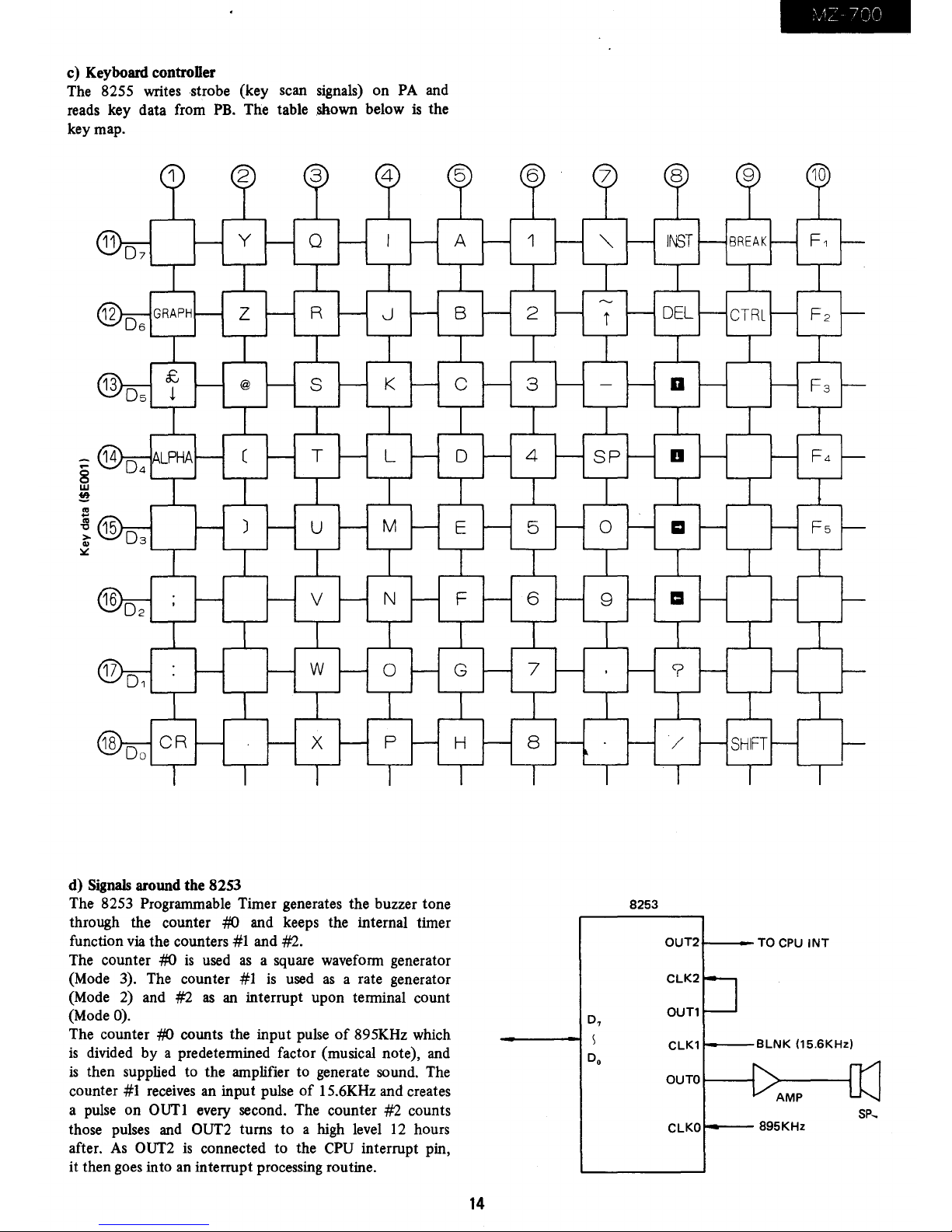
c) Keyboard controDer
The 8255 writes strobe (key scan signals) on
PA
and
reads key data from
PB.
The table shown below
is
the
key map.
d) Signals around the 8253
The 8253 Programmable Timer generates the buzzer tone
through the counter
#(J and keeps the internal timer
function
via
the counters
#1
and #2.
The counter #(J
is
used
as
a square waveform generator
(Mode 3). The counter #1
is
used
as
a rate generator
(Mode
2)
and #2
as
an
interrupt upon terminal count
(Mode
0).
The counter #(J counts the input pulse
of
895KHz which
is
divided by a predetermined factor (musical note), and
is
then supplied to the amplifier to generate sound. The
counter
#1
receives
an input pulse
of
15.6KHz and creates
a
pulse
on OUTl every second. The counter #2 counts
those pulses
and
OUT2 turns to a high
level
12
hours
after.
As
OUT2
is
connected to the
CPU
interrupt pin,
it then goes into an interrupt processing routine.
8253
D7
Do
14
OUT2+----TO
CPU
INT
OUT1
ClK1
BlNK
05.6KHz)
OUTO
sp,
ClKO
895KHz
Page 16
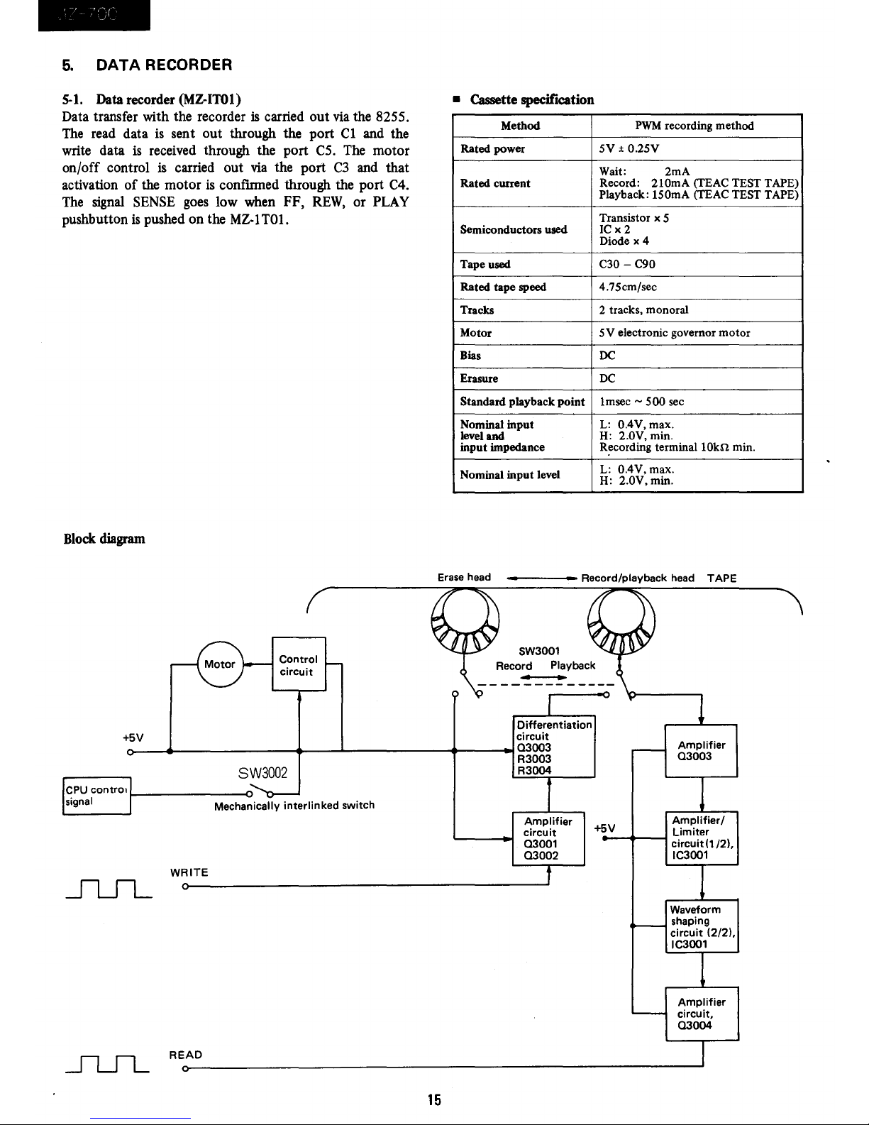
5.
DATA
RECORDER
5-1.
Data recorder (MZ-lT01)
Data transfer with the recorder is carried out
via
the 8255.
The
read data
is
sent out through
the
port
Cl
and the
write data
is
received through the port
C5.
The motor
on/off control
is
carried out
via
the port
C3
and that
activation
of
the motor
is
confmned through the port
C4.
The
signal
SENSE
goes
low when FF,
REW,
or PLAY
pushbutton
is
pushed on the
MZ-}
TO
I.
Block
diagram
+5V
Control
circuit
• Cassette specification
Method
PWM
recording
method
Rated power
5V
± O.25V
Wait: 2mA
Rated
current
Record:
210mA
(TEAC TEST TAPE)
Playback:
150mA
(TEAC TEST TAPE)
Transistor x 5
Semiconductors used
IC x 2
Diode
x4
Tape used
C30 - C90
Rated
tape
speed 4.75cm/sec
Tracks
2 tracks, monoral
Motor
5V
electronic governor
motor
Bias DC
Erasure
DC
Standard playback
point
lmsec -500
sec
Nominal
input
L: O.4V, max.
level
and
H: 2.0V, min.
input
impedance
R~cording
terminallOkn
min.
Nominal
input
level
L:
O.4V, max.
H:
2.0V, min.
Erase
head
------
Record/playback head TAPE
Differentiation
circuit
o-
__ ~ ______________ ~ __ ~ ____________ ~ ____
~03003
R3003
R3004
Amplifier
03003
SW3002
Mechanically
interlinked
switch
WRITE
READ
15
Amplifier
Amplifier/
circuit
+5V
Limiter
03001
-~---!
circuit(1/2),
03002
IC3001
Waveform
shaping
circuit
(2/2),
IC3001
Amplifier
circuit,
03004
Page 17
I
iv1Z
700
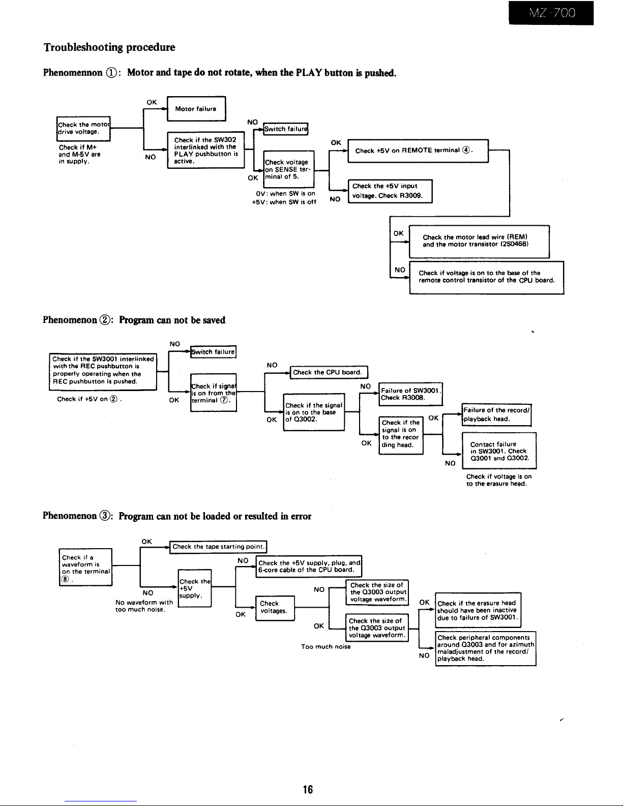
Troubleshooting procedure
Phenomennon
CD:
Motor
and
tape
do
not rotate,
when
the
PLAY
button
is
pushed.
Check
if
M+
and
M·5V
are
in
supply.
NO
Motor
fai lure
Check
if
the SW302
interlinked
with
the
P
LAY
push
button
is
active.
Phenomenon
@:
Program
can
not
be
saved
Check
if
the
SW3OO1
interlinked
with
the R EC push
button
is
properly
operating when the
REC
pushbutton
is pushed.
Check
if
+5V
on
Cl)
.
NO
itch
fai lure
heck
if
signa
is
on
from
the
OK
terminal
!J).
OV: when
SW
is
on
+5V:
when
SW
is
off
NO
Check
+5V
on
REMOTE
terminal
@.
Check
the
+5V
input
voltage. Check
R3009.
OK
Check the
motor
lead
wire
(REM)
and
the
motor
transistor (2S0468)
Check
if
voltage is
on
to
the
base
of
the
remote
control
transistor
of
the CPU board.
Check
the
CPU
board.
Check
if
the signal
is
on
to
the
base
OK
of
03002.
Failure
of
SW3OO1.
Check R30OS.
signal
is
on
to
the recor
OK
ding
head.
OK
NO
Failure
of
the recordl
playback head.
Contact
failure
in
SW3OO1.
Check
03001
and
03002.
Check
if
voltage
is
on
to
the
erasure head.
Phenomenon
®:
Program
can
not
be
loaded
or
resulted
in
error
Check
if
a
waveform
is
on
the terminal
®.
OK
Check
the
1...----1+5V
NO
supply.
No
waveform
with
too
much
noise.
NO
16
Check
if
the erasu
re
head
should have been inactive
due
to
failure
of
SW3001 .
Check
peripheral
components
around
03003
and
for
azimuth
maladjustment
of
the record I
playback
head.
Page 18
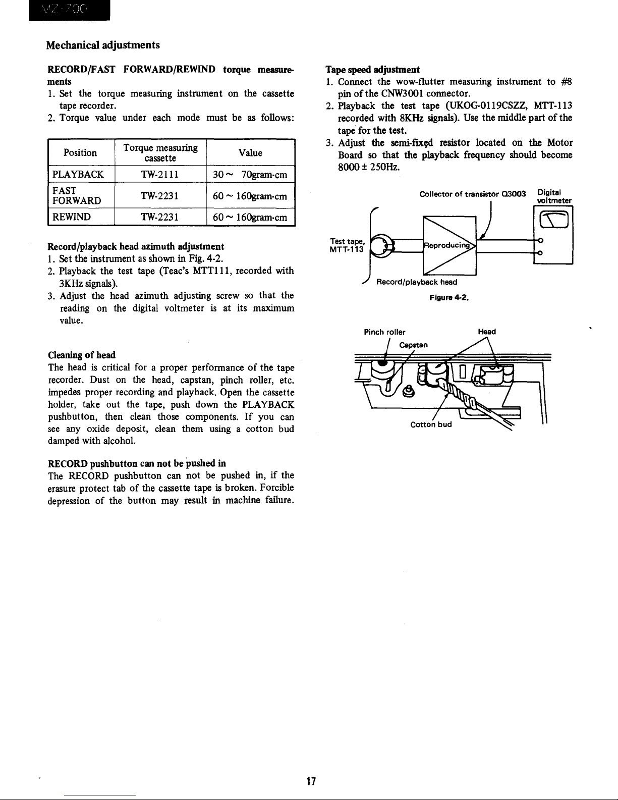
Mechanical adjustments
RECORD/FAST FORWARDjREWIND torque measure-
ments
1.
Set the torque measuring instrument on the cassette
tape recorder.
2.
Torque
value
under each mode must be
as
follows:
Position
Torque measuring
Value
cassette
PLAYBACK
TW-2111
30
'"
70gram·cm
FAST
TW-2231
60
'"
160gram·cm
FORWARD
REWIND
TW-2231
60
'"
160gram·cm
Record/playback head azimuth adjustment
1.
Set the instrument
as
shown in Fig. 4-2.
2.
Playback the test tape (Teac's
MTTlll,
recorded with
3KHz signals).
3.
Adjust the head azimuth adjusting screw
so
that the
reading on the digital voltmeter
is
at its maximum
value.
Cleaning
of
head
The
head
is
critical for a proper performance
of
the tape
recorder. Dust on the head, capstan, pinch roller, etc.
impedes proper recording and playback. Open the cassette
holder, take out the tape, push down the
PLAYBACK
pushbutton, then clean those components.
If
you can
see
any oxide deposit, clean them using a cotton bud
damped with alcohol.
RECORD
pushbutton can not be pushed in
The
RECORD pushbutton can not be pushed in,
if
the
erasure protect tab
of
the cassette tape
is
broken. Forcible
depression
of
the button may result in machine failure.
17
Tape speed adjustment
1.
Connect the wow-flutter measuring instrument to
:f#!,
pin
of
the
CNW3001
connector.
2. Playback the test tape (UKOG-0119CSZZ, MTT-1l3
recorded with 8KHz signals).
Use
the middle part
of
the
tape for the test.
3. Adjust the
semi-fix~
resistor located on the Motor
Board
so
that the playback frequency should become
8000 ± 250Hz.
Test tape,
MTT-113
Pinch
roller
Collector
of
transistor
03003
Digital
voltmeter
Figure 4-2.
Head
Page 19

MZ~700
Cassette
recorder
waveforms
Primary stage amplifier
output
wavefonn
Operational amplifier
input
wavefonn
Operational amplifier
input
wavefonn
CD
®
®
/1
AWl
IJ
1.
~
6mv~
1.8V
r
vpp
pp
T
ov
Operational amplifier
input
wavefonn
Operational amplifier
output
wavefonn
Output
wavefonn
@
® ®
Tt
f1
" "
T
T
1.SVpp
4Vpp
sVpp
1
\lV""~'"
1
1
Recording
input
wavefonn
Recording signal amplified wavefonn Recording signal amplified wavefonn
(J)
®
®
T~
-
-
-
T-
r
~
T
~ ~
1.SV
O.9V
1.8Vcc
pp
pp
1
~
....
....
1
'-
'--
'- '-
....
Head
input
wavefonn
@
I\
~~
\
1\
V /
V
o Figure in a ciele represents the waveform test point on the circuit diagram.
18
Page 20

~\;1Z
700
5-2.
External recorder playback circuit
When
the external recorder
is
used, connection
is
made
with the 8255
by
shorting P-12. In this condition, the
write data (8255
PC
output)
is
differentiated and sent
to the recorder.
In
the case
of
read, the signal peak
is
chopped by
DI
and D2 (about
O.6V),
amplified in the
1.2V limiter (about 1.2V), then amplified
to
5V in the
next stage amplifier. The phase
of
the read signal may
be
inverted with the tape switch after this
is
to compensate
for phase difference owing to the head
of
the recorder.
When
proper operation
is
not attained with an external
recorder, adjust the volume control and the tone control
knobs to optimum positions. Those which incorporate
treble and base for tone control should preferably be set to
a flat condition, and those with only a tone control knob,
should be set to a high condition.
6.
COLOUR ENCODER
6-1. Colour encoder
• The encoder unit should
be
replaced
as
a unit part.
• Input signals
• COLOR
•
CSYNC
•
HSYNC
•
VSYNC
• R
• G
• B
Colour sub-carrier
wave
frequency
Composite synchronizing signal
Horizontal synchronizing signal
Vertical synchronizing signal
• CVIDEO
'X.
Rear
view
,~
B/W-Colour
sw
I + +
6+
? I
RF
CH1-
VIDEO
8pin
OUT
CH2
OUT
Din
SW
19
• 8-Pin DIN connector
I VIDEO
2 GND
'5'
VSYNC
4
HSYNC
'3'
CSYNC
6 R
7 G
8 B
7~~
3 •
S'
8 4
2
• Whenever there
is
any problem with the display check
if
all
signals are supplied to the colour encoder. Check
the waveform
of
VIDEO OUT.
* Problems may arise
if
the colour TV
is
improperly
adjusted.
Signal waveform
of
VIDEO OUT (figures in the drawing
represents nominal values)
0-
--
64
Page 21

7. MICRO
COlOR
GRAPHIC PRINTER
7-1
Micro color graphic printer
1) Block diagram
H
H
Con-
Buffer
nectar
~
rr-
(1) At power on
/
I'
\
,
Intelligent
J
interfacing
LSI
~
I"'-
Control switches
{paper feed
Reset
Pen exchange
At power on, more than
SV
of
pen up current
is
applied
for a period
of
IOms,
plus 5 and minus
Oms,
to move the
carriage 556 steps backward on the
X-axis
in order to
initialize the colour position.
As
the carriage
is
held at the
left margin after disengagement
of
the motor, it
is
then
moved 30 steps forward on the
X-axis,
then stepped back
30 steps
again
to check
if
the colour position detector
has been made.
If
not, it continues to move the carriage
30 steps forward on the
X-axis,
then return 30 steps to
ensure the made condition.
(2) Colour change operation
To change colour, the slider makes three reciprocating
movements
of
6mm (30 steps) at the left end
of
the
X-axis
to move the pen position one step.
When
the desired pen
position
is
attained,
it
then returns to the home position.
Since the pen rotor makes a unidirectional rotation at
the left end
of
the
X-axis,
and
is
locked within printable
range, care must be exerted not to touch the rotor and
the slider.
20
MZ-700
.....--
-
\
I--
~
V-axis
,
I--
stepping
motor
J
Drive array I
l-l.
I--
X-axis
~
stepping
I--
motor'
I
~
Pen
up/
"
Magnet
down
drive circuit
"7
magnet
I
L_
I
_J
Printer mechan
ism
(3) Pen exchange operation
A pen needs to be exchanged with a fresh one when
it
runs out
of
ink. In such
an
event, the pen
is
moved 485
steps forward on the
X-axis
from the home position with
the used pen located on the top
of
the rotor, then take
out the used pen, by pressing the pen release
lever
and
exchange it with a fresh one.
(4) Motor phase and rotating direction
The arrow head indicates the forward direction for both the
X-axis
and
Y-axis.
~
~
5.
~ci,.a..L.-t
b
~
L"L.
(A
"'5~
hL
'::"$'~
~
kot
......
.-J
Page 22

2) Pen exchange method
To remove pen, press the pen exchange button, when the
slider
is
at the right handside, push the pen release lever.
Motor
Push
the
pen release lever
To install the pen, push the tip
of
the pen through the
ring
of
the return spring in the nrst place, then push into
the holder. Upon completion, ensure
that
the tip
of
the
pen
is
engaged with the hole
of
the pen return spring.
If
colour change
is
done when the pen
is
disengaged from
the hole, it may cause improper rotation
of
the rotary
holder
as
the slider makes contact with the pen. Do
not
try to rotate the rotary holder
by
hand when installing
the pen during replacement
of
the pens.
• The X-axis stepping motor and the Y-axis stepping
motor are driven
by
the two-phase magnet.
Stepping
motor
driving signal
Basic
drive pulse
n
n n
t---
Phase
A
Phase
B
Phase
C
Phase
0
Motor
clock
Hold
period
~
tMH
21
It
is
more effective to
save
power
to
shut
off
current
while the X and
Y axis motors are
at
a halt. But, there
may be a possible malfuction because
of
unsuppressed
vibration,
if
the current
is
turned
off
with a normal
pulse width.
In
order
to
prevent this, current
is
applied
excessively for more than the given hold time (tMH
=
1 ms
or
more).
• Colour position detector
The colour position detector consists
of
a reed switch
and a permanent magnet and
it
may cause malfunction
owing
to
external vibration, and magnetic influence.
Especially, when deposit
of
alien matter
or
paper
frag-
ments is between the left end
of
the carriage and the
frame this may result in a failure
of
the colour detect
performance.
• Character set
Input
of
an undefmed code
up
to
$20
is
ignored. Other
undefmed codes are represented in hexadecimal notation
using the pen in a
next
color pOsition.
Pin configuration
(top
view)
TO
Vcc
XTAL1
T1
XTAL2
P27
RESET
P26
SS
P25
INT
P24
EA
P17
RD
P16
PSEN
P15
WR
P14
ALE
P13
DBo
P12
DBI
P11
DB2
P10
DB,
VDD
DB4
PROG
DBs
P23
DB,
P22
DB,
P21
Vss
P20
Pin Configuration
Page 23

,
MZ--700
[COLOUR PLOTTER PRINTER CONTROL LSI]
Pin
assignment
Symbol
Name
In/out
Function
Vss
Ground
Connected
to
QV.
Vcc
Main power Connected
to
SV.
VDD
Power
Connected
to
SV.
PROG Program
Out
Not used.
Plo -PI
7
Port I
Used
as
printer control signals.
P20 -P27
Port 2
Used for data input port from
CPU.
Do
-D
7
Data bus
Used for stepper motor control signals.
To
Test pin Q
In
Input from pen change switch.
Tl
Test pin I
In
Input
from paper feed switch.
.
INT Interrupt
input
In Data transfer strobe
MZ·
700 -+ MZlPOl.
RD
Read signal
In Not used.
"
WR
Write signal
Out
Not used.
RESET
Reset
In Used
to
initialize the processor.
ALE
Address latch enable
Out Not used.
PSEN
Program store enable
Out
Not used.
SS
Single step
In Not used.
EA
External access
In Active when EA
=
QV.
Pins used
to
attach the crystal oscillator or
RC
network
to
Xl,
X
2
Crystal inputs
In generate internal clock. However, external clock signal may be
inpu tted through these pins.
,
22
Page 24

,Q
700
7-2. Interfacing with the MZ-700
Fig.
1 shows the block diagram for connection with the
printer.
Fig.
2 shows its circuit description. Fig. 3 shows
the timing chart.
Table
of
character set
Figure 1. Block diagram
00---1
00---1
AROP---t
ROA---;
Buffer
~
LSD
0
I
2
3
4
5
6
7
8
9
A
B
c
D
E
F
0 I
W
[1]
B
0
[8J
[g
2 3 4
5
sp
0
@
p
0
1 A
Q
""
11
2
B
R
#
3
C
S
$
4
0 T
%
5
E
U
8x
6
F U
/
7 G
W
C
8
H
><
,
9 I
'I
j
*
c
J
~
c
+
c
K
[
5
5
<
L
""
-
-
M
]
-
c
>
N
t
/
?
0
~
MPU
The
CPU
sends data to the printer after confirming that
RDA
is
in low state. Five micro seconds later, the strobe
signal ARDP goes high. The
CPU
confirms that RDA
is
in high state, ARDP
is
returned to a low state 14.5 micro
seconds later.
6
7
c
i
I
8
>
A
9 A B C
q
n
0
-
e
z
U
"
w
m
"v
S
u
t
,
---1
1
9
0
h 0
I
k
A
b' f
- -
0
- -
X
V
01
d
i
r
uiyl
PI,B i {
C J
=
TranSistor
array
Solenoid
driver
D
=
Functional
Switches
PAPER FEED
PEN CHANGE
ROA
-----,
E F
1
[
\~
\
[
Color
position
detector
X.axls
stepping
motor
Y.axls
stepping
motor
PEN
UP/Down
SOlenoid
DATA
______
~~~------~------
I
I
I
A
ROP
------r-----I,
L
1
I
-I
Figure 2. Interfacing
timing
-+---i-: --5,us
1
14.5 1
I
,
,us
23
Page 25

8.
POWER SUPPLY
Power supply circuit description
(1)
AC
source power
is
rectified through the diode bridge
(RB-156).
(2) Current flowing through the primary coil
of
T1
is
switched by means
of
Q 1
so
as
to induce electromotive
force in the secondary coil. To protect voltage fluctuation on the primary side,
Q2
is
implemented, which
will
become active to deactivate
Ql
by dropping the
base
of
Q1
to
GND
when voltage increase occurs on
Q2.
(3) The electromotive force induced
in
the secondary
coil
is
rectified through D21, and DC5V
is
derived
from the network consisting
of
C22, C23, and L21.
TROUBLESHOOTING
1.
Trouble kind
a:
w
I-
..J
u:::
w
en
(5
z
a:
!!!
u..
~
U
w
a:
Because different location has to
be
repaired depending
on a kind
of
trouble, you have to check, the output voltage
in the first place. (Apply source voltage
of
220 to 240V
with a 3.75A load connected
on
the output.)
There are following four cases:
1)
No output
(OV)
2) Low output
(1
to 4V)
3)
High
output (7 to 10V)
4) Abnormal increase
of
output ripple (several hundreds
millivolts)
021
in
failure
(!)
~
J:
U
I-
~
en
..J
o
a:
I-
z
o
U
MZ-700
(4) For circuit stabilization against load fluctuation,
we
use
IC21
(shunt regulator),
PC1
(photocoupler),
and
Q3
(transistor).
When
the gate
of
IC21
is
above
2.5V after sensing the
5V
output by means
of
R22,
VR21, and R23, it makes
IC21
active and then
PC1
active.
As
the
base
voltage
of
Q3
increases with activation
of
PC1
photo-transistor,
it
makes
Q3
active
and drops
the base
ofQ1
to
GND
so
as
to turn offQ1.
Although it
is
possible to adjust the
DC
5V
voltage by
means
of
VR21, it needs to
put
the
CPU
PWB
into
connection.
a:
w
~
a:
0
u..
en
Z
~
a:
I-
a:
W
u..a:
-w
1-1-
U..J
w_
a:u..
w
U
Z
w
en
2. Finding where
is
in
trouble
2-1. In the case
of
"No output
(OV)"
N
Observe waveform
between
the
collector
and
emitter
of
01
(*1 )
01
or
01
in
failure
24
01,
R1
in
failure
R5,
02, 03,
R3,
03
in
failure
(*1):
If
the output voltage
were
to
be
still
OV
without
blowing the fuse after replacement
of
Q1,
proceed to
steps described to the left
of
the troubleshooting
flowchart.
,
Page 26

Waveform
CD
Waveform
CID
Waveform@
"1
320V
-------ov
_____
""'lov
2·2. When extremely
low
output
voltage is
encountered
I
If
Waveform @
I
R5,
RS
in
failure
Waveform@
Several volts
or
more
..LI
----~--~----ov
(
Start
I
Observe waveform
between
the
collector
and
emitter
of
Q1
I
I
If
Waveform@
I
R9, C12,
C",
Q3
in
failure
Waveform@
Unstable waveform
-
~
\
2·3. When extremely high
output
voltage is
encountered
(7 -
tOy)
PC1,Q3,R7,RS,C11
in
failure
N
25
1
If
Waveform(§)
I
PC1, IC21, C25
in
failure
Waveform(§)
R21, PC1, IC21, R22,
R23
in
failure
Page 27

2-4.
Abnonnal increase
of
output
ripple
In
case
irregular increase is seen for the output ripple like
the one below, it needs to replace C22 and
C23
with new
ones because they have been fatigued.
-
t
t
1
00m V or
less
(Normal rippla)
Several
hundreds
millivolts
(Abnormal
ripple)
26
Input:
AC220 -240V
Output:
5V,3.75A
Usa
oscilloscope
~v1Z
-70C
Page 28

9.
le
SIGNAL POSITION
74LSOO
74LS02
74LS14
7417
5A 5Y
IY
2A
2Y 3A
3Y
GND
lA IY
2A
2Y
3A
3Y
GND
74LS42
7472
VCC
PR
K3
K2
NC
CLR
JI
J2 J3
GND
74LS125A
74LS145
INPUTS
£
VCC
4C
4A
4Y
3C
IC
lA
IY
2C
2A
2Y
GND
27
74LS04
74LS32
74LS86
\ICe
48
4A
4Y
38
3A
lA IY
2Y
GND
74S157
SELECT
~
IV
~
2V
GND
INPUTS OUTPUT INPUTS OUTPUT
Page 29

74LS166
74LS246
74LS367A
VCC
G2
5A 5Y
4A
lA
IY
2Y 3A 3Y
GND
74LS174
I
CLEAR
IQ
ID
I
I
CLEAR
IQ
74LS273
BD
70
74LS176
OUTPUT
IQ
ID
2Q
3Q
28
2Q
GNO
Page 30

MZ-700
.
10.
CIRCUIT DIAGRAM & PARTS LAYOUT
29
Page 31

Co.)
C
EXRESET
,---.
"'0
RI07
ICCH
'0'
IK
LSOO
10r-"
.J
/0
""
~,
220
C24
1),I/50V
10-
-
5V
IC CH
LSOO
"
"
12
.5V
'of
IC7F
RIOI
lSI4
10'
11
Ti
10
,~
.
c
••
I
1_22.J1/16V
III
Tantalum
5V
1109
",
co.
~~,.
IRe",
IC6F
LS02
12~13
--!!...}
./
le
7F
LSI4
~-
~,.
le7F
lSI4
ICe.
IQ
f'L--
ICL
r.----J
18
5V
lA
I
~
LS32
5
I •
1
IC6G
LS32
~RI)
_
==-::..
3 --.-----<
MREQ
IC
6G
lS32
RESET
8255
RESET
RESET
le
7G
"'02
f
Z-80A
S04
330
,
•
.
~
~--l
26
RHft
'"
R59
R7
ftr
3.31<
3.3k
Niii
1
iNT
IC
IF
lS367
RFSH
-----2-
2
Mi-----2-
·
WR
------L
-<;}
•
RI) ------!
10
IORO
----!!
,.
"'REQ
-------.!.!
14
G,
G2
I'
['
IC
4G
LS367
HALT
---2.
2
A'
------!
·
A2
----2
-<;}
·
A,
------!
'0
Ao
----!.!
,.
8US
~-------.!.!
r----<
~
Go
G2
l'
I"
IC
6F
lS02
IC
6F
-
6~
lS02
MI::::::=:;:J
INTAC
3~
IORQ
"::>
5
./4
-;-) I I
IC
7F
lsr4
17
NMI
25
BUSRQ
16
INT
28 RFSH
27
Mi
22
ViR
21
RO
20
'iORQ
19
MREO
WAIT~
WAft
IS
HALT
!3
A3
"
A,
31
AI
'0
Ao
+~vo------!.!
Vcc
,r-!.!
GNO
A"
,
A,.
·
AI3
3
A,.
2
All
,
AIO
.0
Ag
39
As
38
A7
37
A6
36
A,
"
A.
,.
07
"
06
10
0,
·
O'
7
•
0,
02
12
0,
"
Do
14
SUSAK
~
.~~.
IC7F
IC7F
LSl4
lSI4
le
4£
LS367
10
•
·
,
12
,
{:f>-
·
,
,.
,
2
,
G,
G2
,
r'
IC
4F
lS367
2
, · ,
•
{:f>-
,
'0
,
12
I
,.
I
ili
Gz
I
"
IC
IG
lS245
z
I , I
·
I
'Q'
• I
7 I I
•
I
·
,
G
OIR
to
,
A"
AI4
A"
A,.
All
Alo
••
A.
A7
A6
A,
A.
07
O.
0,
0'
0,
02
01
Do
......
n
."
c:
er
Q
a
n
~.
::t
-.
-
'-'
........
Page 32

Co.)
0,
21
07
O.
OB
00
0'
>--
..
0'
o.
0'
0,
0,
D.
tiiA
'
RO
II1W
WR
AI AI
Ao'
• Ao
c:sEO~CS
8255
;'s
RESET
RESET
,ooP
COOl
+5V~VCC
D
OND
le
BE
8255
+.v
ICBJ
05.
0)
~
06
IS
1~'8
RU,"
PC,
:~I:
'f::/16V
READ
P-8
le
3e
C04069
.,,'"
~~
".
0,,,.,
B TAPE
sw
en
' • 0 WRITE
00,".'
le
3e
i:~
coo
12"
00
'1
P-7
n
le3e
.0, t!t-
.,
e040.9
.
le
3e
le
3e
c,
""..
.0
",
..
,
..
l.lI(:
P-12
r---
__________________________
~o~
pc,I"
1
'cxC
l
1
pc,
pc,
PO.
Plo
It
PO,
..
PO.
20
PB ..
22
PIS
IS
PO,
,.
PI,
"
PA.
0
PA'~
PAo . PA.
le
18
~"
!C3e
22.
~
-----+-----.
LSOO
~
i
+
."
_<20
2Z..,IIIV
.v
12
0 PR
0
1
I' 1 , 1 'IJ:>!.
fe7E
LS7
..
~eK
~J!-..
le
BC
RI03
7417
Ik
t;:
CL
.C47
13
IK)OP
~
__________
~IO~
,,"c.
C44
le
le
I .coOp
I
lOOP
LS04
5V
ffi
A.
>---+--'-'-<
A,
IC6E
lS42
.vo--f;I-
IOO~:.oV
07
01
ItAG
8255C
I
ICeH
OUT2"
INTMSK
>-:V.
--
INTI
..----
" e
..
I
gill
••
10
7
,.
I'
..
)
"
)
"
)
/0
00
I
0
•
,0
0
.
3
"D
..
A
~~
I~
3"
0
L-
~~
I~
L---
le
AE
74L$145
P-'
•
O.
CLK2 .8
GATE2
'6
+5V
O.
D.
D •
Do
D.
OUT I
ClKO
RIO'
3.SIC
CSEl
tMi'i
MW
Ao
A.
GATEOI'°-'-o
----------,
D.
MW
::::::;=r=t----4
csn
1C6F
LSOZ
5V
1.
_
~
iilID
EMR~
oP-
ICCH
LSDO
D.
O.
0,
IOII:VR~~-4C
5V
'54
S.SI(
EX WRITE
EX
READ
WRITE
READ
SENSE
MOTOR
P-3
..
~
+.v
Cl.
_
~O.I
...
/12V
GNO
JII
JI'
HIiJ(
5V
Y
Rill
2.2IC
leeH
LS221
I
coo
0.00
LOAD
• RET
OUT
DtSC
II
J1VLT
THRI'
le
8J
5
..
T'
SOIN
5V
+.V
'till
1.8"
,tIIO
...
C
..
I,,/SOV
........
~
r
a
n
;:i"
c::
=:
,-..
~
Page 33

~
IV
0 , T
"1
ClO
S!fIIIIY
Tantalum
Iv
0
"'
5v
0 "I
5v
0
"1
5V
0
"'"
5 V 0
"'
5 V 0 "I
5V
0 -I'
Ao
A.
AI
A,
Az
AIO
A!
All
A4
Alz
45
AI!
A6
AI4
A1
AI'
V
'0
le7G
504
le7G
$04
6
"PT I C SEL
1>'
<
Rn
1>'
:Wi\
IC5H
2732
A"
:==~t':tA~
Ao •
Ao
A,
22
At
AI
AT
A'
As
"4
A.
A.
A,
m
I'
, , I I I I I I I :
Do
I'
• I I I I I I :
0,
"
I' , • I I I I I :
D.
I"
, , I I I I :
D.
I' , , I I I :
04
I'
• I I "
D.
I'
,
leD.
r
c~
......
n
(!
go
a.
a·
...
....
-
W
-
.......
Page 34

Co)
Co)
for
4KB
ROM
le
BD
~I
D'~
I.
D'~
"
D.~
0=
D'~
D.
>----.!
I.
. ,
Dz
-.-!.
D,
>----.!
,.
Do
>----.!
11
;J1
,
,.
iiD
eTI
.V
VIO
ViO
11
123
lal
0."
3.3K
ffj(
IC60
7417
SYN
Hfi
IC
AD
LS245
.V
..
,
220
~
...
'20
HfiNC
.v
IC6D
k
7417
220
sf'.........
6 VSYNC
IC
3A
lSl74
zr-I··
D,~
I':
, 1 I
:1'
D
.-
-CG32
D6~1
I
I"~
, ,
,2D
,
"3D
RIO(
Vell(
~
VIO
>
IC6D
1417
.V
J:
oz
"
z "
,t,Y.I
ICIA
.,1.1!!!1.
:::HiI
"\.,.
ICIO
7417
.V
D~
I
D:
• 0
1
D'
r.
• I
D.
'
DI~I
I:
,1"'"
:'4D
4O~-
BACK
.LCs~~
I"
, I I I I I I I
.D
501!L-t--, ro'
11
.i.
"I6D
",,!JL+
~
,
,.
Ill>
IC2A
.,........,
~'I
'ri
I}:.-----::z::-.:'o.
.~'
GT.
LOAD
.V
IC2A
.
RESET
,,>--------'
110
III h
114
lis
...
111
02
DJ
04
05 01
or
~IO
I.
PlO
02 03
04
Os
0.
01'
01
Alo
I PlO
It
BA
2016p·
I
A,
ICAA 20tc5P-1
A,2
P,
A.
p,
Aa
23
p,
LJ~~~¥..~.~.~M~.~A'~,J
A
. ,
ViO
..
220
)"-
............. - C
VIDEO
.V
~
.,
ICTD
IK
LSOS
~
"
11
M
EXINT
I 1C4A LSlO
•
~
~
WE
•
fe4A
L$IO
IiIIf
eT2
le
lA
All
>-......,1--1-'-1...
WE>'--~--------------------------------~
LSOO
,1C4A
LIlO
5157
.-0
p,PzP,F'4PsPt;P.,
8TI
Ail
All
~W"'IT
,.....,
~
I
~.
=:
~
'-'
Page 35

p,
p,
P,
P.
'0
P,
P.---"
--B
Pr
,.
"
p.
c..:I
p,
.j:lIo
p,o
07
5157
SYN
CLK
obe
BLNK
COLR
HBU<
SEl
PoLOAD
HSY
NIP
03
Q2
Or
~
WA
vEl.K RESET
"
le
7A
M60719
"
0
120
,
,
•
.
,
7
•
10
11
12
13
114
11'
III
5IR6SIA671R68IR691R70IRll IR72IR73IR1'4IR75IR761"71IR70IR79IR80 R65 -
R80
Ao
AI
A2 A3
A4
As Aa
Ar
Aa
A9
AIO
An
AI!
AI3 AI4
AI'
IK
23.
vcc
53:GNO
44:
abc
(not
uSed)
220
.16
SV
07
o.
0,
o.
o.
0'
0,
Do
Wo
Rii
IORQ
MREQ
,"0
RFSH
RAS
SV
CSO
GATE
CL
ill
t>
~
PRC
Rii
ViR
Ao
~
s:'OO
NIP
GATE
CL
5A~~
17.73
MHz
~tlJ
~
~
I 7
70
70
J!!---J
..
20 20
5
~
•
ID
IQ'
,
BD
_f
BC
"
~
7 3D
3Q~
14
60
60"
~
•
40
4Q'
1
13
50
5Q
12
IT
le
4J
~
.
40
4Q 2
13
3D
3Q
.,
IC5J
~
tt
~
0
5~Wi
' ,
~C
4
'
WO
1
~B
Z
pL!l-0
;.--.-!l
A
i
'----
IC
ZG
RESET
~
I •
'PN
IC
ZG
.
,
4t-J
IC
ZG
11
12
13?fJ
le
2G
.
2
,
~
("J
"'Cl
c::
r:r
0
I!i
Q.
P-I
le
2H
.--
,
ARDS
7417
"41,R40
1~12
V~ll.,"2
ClO
n
~
.
~
RO.
...
.
....
·
AR07
le
2H
IM3.R42
.
.
V~5.R14
CII
,-,
V.
R07
'-'
---
7
ARD6
le
2H
1M5,JM4
11
'0
\I
Rl7,"1'I
02
ROS
•
ARD~
le
2H
ft47,R46
,
•
V~9.RI.
Cl.
RD.
,
ARO"
~
1M9,R48
' .
V
RZI.R20
CI4
Ro"
·
ARC3
~
7417 "5.,"50
I 2
V~,3,RU
RO'
·
AR02
K
R!o3,FlS2
13
12
V~25,R24
ClI
RoZ
2
ARDI
K
R",R~
. .
V~21.R21
07
Rol
INT
----...
!'0o-
~l--r----~-I-?
'''-
IC
2H
AIRT
l /
7417
R39,A31!
I/"II,RIO
,
2
"
IRT
ARDP /
/
R57,RSE
11
'0
V~29.A28
Cl.
RoP
/
/
le
2J
kif)
7411
"0-
::~:
i
SV
"
"A
SNS
RoA
...
n·"
"0
<30
R8
~C1
-<.
STA
390,
I lOOP
RoA
.v
:~
:
~~37
,'5>-
..
0
1"0-
R
.~
~
~ca
390
IIOOP
L....-
~
ID
r------------,
I
5V
R38_
R51 I
I I
I I
I
..'L
0 I
I I
I
I'OOP
I
I I
L
__________
...l
Page 36

w
U'I
I
2
3
4
5
6
7
8
9
10
11
12
13
14
15
P-I
ARDP
ARDI
ARDz
ARD3
ARD4
ARD5
ARD6
ARD7
ARDe
AIRT
GND
ARDA
GND
ASTA
ALPS
P-5
I
+
5V
I
2 + 5 V
,
3
3
GND
5
4
GND
7
9
11
13
IS
17
19
21
23
25
P
-10
RDP
2
GND
49
RDI
4
GND
47
RDz
6
GND
45
RD3
8
GND
43
RD4
10
GND
41
RD.
12
GND
39
RD6
14
GND
37
RD7
16
GND
3S
RDa
18
GND
33
IRT
20
GND
31
RDA
22
GND
29
STA
24
GND
27
FG
26
FG
2S
23
21
19
17
15
13
11
9
7
5
3
I
~
("l
."
<::
~
Q
a
-
n
e
P-II
P-13
P-9
a"
e-
n
AI5
NMI
50
AI.
EXINT
48
A
13
GND
46
Alz
MREO
44-
Q
0
GND
::s
2 0 C
SYNC
f
3
0
CVIDEO
i
0
HSYNC
c"
4
::s
I
5V
2
VBLK
3 JA I
4
JA2
All
GND
42
5
GrvD
........
5
0
V
SYNC
Alo
10RO
40
6
0
GND
A9
GND
38
7
0
+5V
Aa
RD
36
8
0
G
A7
GND
34
9 0 B
A6
WR
32
P-14
10
0
R
A.
EXWAIT
30
I
5V
11
0
COLR
A.
Mi
28
2
VIiIT<
12
0
GND
A3
GND
26
3
JB
I
Az
HALT
24
4
JB
2
AI
EXRESET
22
5
GND
Ao
RESET
20
BUS
<T>
GND
18
07
GND
16
06
GND
14
D.
GND
12
04
GND
10
03
GND
B
Dz
GND
6
01
GND
4
Do
GND
2
Page 37

I
Power
unit I
SOl
AC240V
Lt:.
"
T500mA
A.
L'
l.,L},
Z0040
Cl
RBt56
RI
C7
A\
T I
10/2W
t~/(OD
~
ZOQ74
r%~~~----~--~
" e
l!",F/"OO
.2
"
68
K/2W
0'
ESIF
QI
"
2201C/IW
"
",OOP
••
"0
.1."
I
3300pF/
..
OOV.2
25C31
50
"
'50
"I
Q2
2SC
12130
. ,
I/I
W
Q3
25CI2130
ell
o.
,~
.22
331(
10
C26
C2)
R21
0 IIJ l000Jj/IO
."
'"
0.0:5311
VA?I
"
---:~,,
le21
TL431C
Rn
2.71<
5V
G
Page 38

[Colour encoder circuit]
'~
f
'00"
-
IOv
.l
o.
le,
U/81
co.
'
..
•
•
ICICl/SII
~U/III
.....
•
IClllIS,
GII/III
....
cc,
H07"~P
'"
H07486P
v
•
It
2
Ill'"
JJ
H
'0-
IC2U/41
r~
~n
,
..
,"
-;1'
..
,C,
Cl/4,
ICZ4II4J
.~
"
-,
"
t-
~
8/W
sw.
le I ILF8'
[Main
P.W.B.
for AD-IOO2]
C3001
.Ay
CNW3001
"
-,
..
".
..,
~
'"
...
0'
..
zsc~~p
..
...
1!:
."
••
I~
"
.~,
...
...
oro
~
..
,~.
...
."
..
.
~
.
..
n.
..
~
)t
. "
...
~
..
'"
"
,,~
...
.n
".
'"
:,;~
'0
._
ZI\'
."
Cl
vtt,.
. "
'"
'00,
..
"
...
i~
"
0#
2
SC!M~
I
,
•
,
"
•
'<3
MCI:S12P
00
• •
, ,
tt-
..
,
-
I.~
..
'"
."
.
...
~:7~$O
'"
I
..
-'OO~
~
-
'"
'"
...
'"
'"
'"
..
,
...
.
...
'"
1.1"
'00
, -
..
k
'"
,
..
-
."
0'
.
~~~~5P
~
.
'"
n~
~
...
Ok
...
M
...
"
"
"
"
I-
•
'"
'00
~/
::.:
'"
'"
-
,.
I 0
'0
,-
,~
M'
ff
'
O~
'"
...
:~~
M'
...
~
04
2SC167~
Of
25C945
.
..
:
~
~~
'"
~J'
'
:0
el,
.... '
..,o~
U
u.
'Oy-
2SC~~
O.
0'
25A733
~
25C945
o.,
I .
••
.",.
H
..
p
VlOE:O
OUT
G.o
Page 39

[Motor
P.W.B.
unit]
4
--I\fIIv--
~
Tri
R6
[A()'IOO2j
-
MAIN
PW8
.~
.
".
..
~
[Rot.Sf
HEAD
RECOROI
P\.AVBACK
><£40
-l$
i'
.~
I 1
1
$""'00
REAO
WR
ITE
r-----
----
-
-,
Lf
j-
!"
'"
0
I~
.-
le 3001
}lPC
35B
C
-
I
.-
~:5
005
"
.ro
II
WJ
.~OJ
~2
u..
@ (
o::
~
@ ,
~~:~;
"
••
,
;
r~
nOM
'OK 10"
03001
25C16:52Q
03002"-03004
2SC2021R
BLK
RED
BLK
RED
BLUE
...
;;,
co?
,,~
"
~o
b
;.
t
:f
, .
•
~JV
•
I I
fr(
0.
U
~2S046ec
} TO
MOTOR
~
'-
___
"_,;;""'=TOO
pwe
...
"
Page 40

[Data recorder circuit J
J
I
I
I
~
i.
EI02IAC-33A
o
H
+
~o
N
~o
'"
o
Page 41

.j::o
o
4P
15P
+5V
(POW
ER)
47~/IOV
o
GND
+5V
GND
ARD
ARD2
ARD3
ARD4
ARD
ARD
ARD
ARD
ARD
AST
ARD,
GN
GN
AIR
SEN
+
C3
o
3,;
I.
4
k"~21-=-=-=-=-=-=-=-=-~~=-=-=-=-=-=-=-=~~~~~~~~~~~~~~~~~~?~
0--,
,-,
,
~1!3========~======================~
,j,
I I 6 IC2
r..~======+======================~
I I ,
LBI'"
I~~=====~==~================~
----~+~-:J1:_-22
P21
4
iSi§"====t============
- I ,
~~t:===~====-
________________
_
A
..
"-'"-.0
23
P"
2.,
24
P23
R9
----i---+---
IC
I
'"
r-<>
.5.8050H-059P
",
35
p24
~3~O~-t==~~~1-~~r-1I
__
~
----.;,...-;-
P
13
29
PI2
NC
~
--------l-+----J-r-_3~6p25
33NC
~--------~~~:=tjr-_-37
P26
PI6
27
Plo
"---------<~~~T-
PII
38
p27
1'2~8~~_~~~~~~
6 INT
R3
-
--
Ig~
I
,3::.;9,---...
M
~
_~
------:;
PI,
To
I
31
PI4
~===---------~N:C::=3~2~
PI5
151588
.4
Iq
t
PEN
I
Q2
LPAPE.
CHANGE
I
2SC458KC 4 I
L.
ESET
r
FEED
• SW2 I
'~----"':rv~°V-"T
I r r SW3 r SWI J
--l
~
:,;
rlu_-
~~
]
XB X AXIS
XA
YD
]
YC
Y
AXIS
YB
YA
COLOR
DETECT
SW
+5V
SOL
13P
.......
~
~
"5!.
~
':'
'0
::I.
~
n
~.
5.
-
........
Page 42

Page 43

MZ-700
PARTS LIST & GUIDE
Parts marked
with"
L1I"
is
important for maintaining
the
safety
of
the
set.
Be
sure
to
replace these parts
with specified ones for maintaining
the
safety and .performance
of
the
set.
Page 44

MZ·700
rn
CPU Unit Exteriors
NO.
PARTS
CODE
PRICE
NEW
PART
DESCRIPTION
RANK
MARK
RANK
1
DUNTKl152ACZZ
**
N E
CPU
PWB
2
DUNT-1150ACZZ
BM
N
E
Power
supply
unit
3
DUNT-1151ACZZ
BN
N E
RF
modulator
4
GCDVH1002ACZZ
AB
N 0
Aclyric
cover
5
GFTAR1019ACZZ
AB
N
0
Lid
for
26P
connector
6
GFTAR1020ACZZ
AB
N
0
Lid
for
50P
connector
7
LCHSMI018ACZZ
AY
N
C
Main
chassis
8
PCUSSIOO2ACZZ
AA
C
Speaker
cushion
9 Q S W-K 1 0 1 3 A C Z Z
BH
N
E
Key
board
unit
TSPC-I055ACZZ
AC
N
0
S~fication
label
(MZ
731)
10
TSPC-I056ACZZ
AC
N D
~fication
label
(MZ
721)
TSPC
1059ACZZ
AC
N D
Soecification
label
(MZ
711)
11
XBBSC30PIOOOO
AA
C
Screw
12
XBPSM30P06KSO
AA
C
Screw
13
XBPSM30P08KOO
AA
C
Screw
14
XUPSD30P08000
AA
C
Screw
15
GFTAR1012ACZZ
AB
N D
Lid
for
connector
16
PGUMS1266CCZZ
AA
N
C
Cushion
for
PWB
fixing
angle
17
VSPOO80P-608N
AN
C
Speaker
18
HBDGBIOO2ACZZ
AD
C
Sharp
badge
19
GCABA1006ACZZ
AV
N
D
Bottom
cabinet
20
GLEGG1020CCZZ
AD
D
Rubber
foot
21
HBDGDIOOIACZZ
AB
N D
Model
badge
22
QTANSIOO2ACZZ
AD
N
C
Ground
terminal
23
TLABZ1009ACZZ
AA
N D
Model
label
24
XUPSD26P06000
AA
C
Screw
25
CCABB1005ACZZ
AY
N D
Top
cabinet
26
GFTAT1007ACZZ
AP
N D
Printer
dummy
cover
(MZ
711
721)
27
GFTAT1008ACZZ
AP
N D Cassette
dummy
cover
(MZ
711)
.
28
QTANS1001ACZZ
AB
C
Frame
ground
terminal
29
TLABZ1010ACZZ
AD
N
D
Function
label
-1-
---
-------------
Page 45

MZ·700
rn
CPU
U~~t
Exteriors
I
28
,
7
I
20
P
~
2
If
)
/
19
I
I
I
)
Page 46

I2J
Printer Unit Exteriors
NO.
1
2
3
4
5
6
8
9
10
11
12
13
14
15
16
17
18
19
20
21
22
23
24
25
PARTS
CODE
CCABB1006ACZZ
CFTAT1001ACZZ
CSFTZ1001ACZZ
NSFTZ1001ACZA
NSFTZ1001ACZB
XRESJ40
o 6 0 0 0
DUNTM1051ACZZ
J K N B Z 1 0 0 5
AC
01
LCHSM1004ACZZ
L H L 0 Z 1 0 0 2
AC
L 1
L H L 0 Z 1 0 0 2
AC
RI
PGiDWI001ACZZ
XBPSD30P04KOO
XBPSM30P06KSO
XBPSM30P08KOO
XUBSD26PIOOOO
XUPSD26P08000
XUPSD30P08000
TLABZI027ACZZ
PSPAB1003ACZZ
PZETE1005ACZZ
SPAKA1064ACZZ
SPAKA1065ACZZ
SPAKC1224ACZZ
<
./
'-
'-
PRICE
RANK
AR
AM
AH
AC
AG
AA
BW
AG
AL
AC
AC
AB
AA
AA
AA
AA
AA
AA
AB
AA
AA
AH
AC
AK
5
22
NEW
MARK
N
N
N
N
N
N
N
N
N
N
N
N
N
N
N
N
N
MZ·700
PART
DESCRIPTION
RANK
0
Top
cabinet
0
Printer
cover
E
Pa
cer
shaft
unit
C
Pacer
holder
C Pacer shaft
C
E
type
ring
E
Printer
mechanism
unit
C
Paper
feed
key
top
C
Bottom
cover
C
Pacer holder-L
C
Paper holder-R
0
Pa
cer
lluide
C
Screw
C
Screw
C
Screw
C
Screw
C
Screw
C
Screw
0
Caution
label
C
Collar
for
printer
C
Insulator
sheet
0
Packing
cushion
0
Packirui
cushion
0
Packinll
case
....-1
I I
j }
~18
10
-3-
Page 47

MZ·700
IlJ
CPU
Unit
Electronic
Components
NO.
PARTS
CODE
PRICE
NEW
PART
DESCRIPTION
RANK
MARK
RANK
1
QCNCMI009ACZB
AA
C
Connector to Soeaker (2oin)
2
QCNCMI009ACZD
AB
C
Connector to Printer (4l)in)
3
QCNCMI009ACZL
AC
C
Connector to Colour encoder
4
QCNCMI009ACZO
AC
C
Connector to Printer
5
QCNCM1010ACZZ
AF
C
Connector to Power suoolv
6
QCNCMI0IIACZZ
AE
C
Connector Jov stick
7
QCNCWI013ACZZ
AC
C
Connector to Recorder
8
QCNCWIO~YACi!U
AF
C
Connector to
Key
9
QJAKC1013CCZZ
AC
C
Input jack
Ext
Record/Play back
ID
QSOCZ6424ACZZ
AE
C
IC
socket (24pin)
11
QSW
P1009ACZZ
AF
N
B Push switch
12
QSW
S1012ACZZ
AF
N
B
Slide
switch
13
QSW
S6683RCZZ
AF
N
B
Slide
switch
14
RCRS
1007ACZZ
AV
N
B
X
TAL
(l7.7344MHz)
15
RMPTC8103QCKB
AD
C
Block resistor
(lOKOX8
1/8W
±10%)
16
RVR-B1450QCZZ
AE
B Variable resistor
17
VC
C 5 P U 1 H L
391
J
AA
C CapacitorJ:50WV
39O-,>D
18
VCCSPUIHL471J
AA
C
Capacitor (50WV 470oF)
19
VCEAAUIAWI07Q
AB
C
Capacitor (lOWV 100uF)
20
VCEAAUIHWI05Q
AB
C
Capacitor (50WV 1.0uF)
21
VH
LH0080A/-1
AX
B
LSI
(Z80A CPU)
22
VH
MZ60719GSO
BF
B
IC
23
VH
M2732/ACll
BF
B
IC
(M5L2732K) Monitor
24
VH
TMM2016P
1
AX
B
IC
25
VH
UPD8255/
1
AV
B
IC
26
VH
4 1
64
1 5 0 H
AZ
B
LSI
DRAM
27
VH
8253////-1
BA
B
IC
28
VS
SC458KC/-l
AD
B Transistor (2SC458KC)
29
VS2SD788
C/EC
AC
N
B Transistor
3D
VCCCPAIHHI0IJ
AA
N
C
Capacitor (50WV 100oF)
31
VCCCPAIHH221J
AB
N
C
Capacitor 50WV 220oF)
32
VCEAAA1CWI06Q
AB
N
C
Capacitor 16WV 10uF)
33
VCEAAAICW226Q
AB
C
Capacitor 16WV
22uF)
34
VCEAAAIHWI05Q
AB
N
C
Capacitor 50WV 1.0uF)
35
VCKYPU1HBI02K
AA
C
Capacitor (50WV 1000pF)
36
VCKYPUIHB222K
AA
C
Capacitor (50WV 2200pF)
37
VCSATAICE226M
AB
N
C
Capacitor
(l6WV
22uF)
38
VCSATAICE336M
AB
N C Capacitor (16WV 33pF)
39
VCTYPUIEXI03M
AB
C
Capacitor (25WV 0.010uF)
40
VCTYPAINX104M
AB
C
Capacitor
(l2V
O.luF)
41
VHDDS1588Ll-l
AB
N B Diode (151588)
42
VHiCD4069B/
1
AE
B
IC
43
VHiM74LSOO/
1
AE
B
IC
44
VHiM74LS02/
1
AE
B
IC
45
VH'M74LS04/-1
AE
B
le
46
VH
M74LS08/-1
AE
B
IC
47
VH
M74LS09/-1
AE
N B
IC
48
VH
M74LS10/-1
AE
B
IC
49
VH
M74LS125-1
AH
B
IC
50
VH
M74LS14/-1
AM
B
IC
51
VH
M74LS145-1
AH
N
B
IC
52
VH
M74LS174
1
AK
B
IC
53
VH
M74LS175
1
AG
B
IC
54
VH
M74LS245-1
AM
B
IC
55
VH
M74LS273-1
AP
B
IC
56
VH
M74LS32/
1
AF
B
IC
57
VH
M74LS367
1
AH
B
IC
58
VH
M74LS42/
1
AF
B
IC
59
VH
M74LS74/-1
AG
B
IC
60
VH
M74LS86/-1
AF
B
IC
61
VH
NE556N//-l
AH
B
IC
62
VH
5 N 7 4 L 5 1 6 5 N
AM
B
IC
63
VH
SN74LS221N
AM
B
IC
64
VH
SN74S04N
1
AG
B
IC
(74504)
65
VH
SN74S157
1
'AQ
B
IC
(SN74S157N)
66
VH
SN7417N/
1
AG
B
IC
(SN7417N)
67
VRD-RV2EYOOOJ
AA
B
Resistor
(1/4W
+5%)
68
VRD-ST2EYI02J
AA
C
Resistor
(1/4W 1 KO)
69
VRD-ST2EYI03J
AA
C Resistor{1/4W 1 KOl
70
VRD
5 T 2 E
YID
4 J
AA
C
Resistor
1/4W
100KO
+5%)
71
VRD
ST2EY121J
AA
C Resistor
1/4W
1200
+5%~
72
VRD-ST2EY152J
AA
C
Resistor
1/4W
1.5KO
+5%)
73
VRD-ST2EY153J
AA
C
Resistor
1/4W
15KO
+5%:
74
VRD-ST2EY182J
AA
C
Resistor
1/4W
1.8KO
±5%)
75
VRD-ST2EY183J
AA
C
Resistor
1/4W
18KO
±5%:
76
VRD-ST2EY221J
AA
C Resistor
1/4W
2200
±5%:
77
VRD-ST2EY222J
AA
C
Resistor
(1/4W
2.2KO
±5%)
78
VRD-ST2EY330J
AA
C
Resistor
(1/4W
330
+5%)
79
VRD-ST2EY331J
AA
C
Resistor
(l/4W
3300
J)
80
VRD
ST2EY332J
AA
C
Resistor
(l/4W
3.3KO
±5%)
-4-
Page 48

MZ·700
[3J
CPU Unit Electronic Components
NO.
PARTS CODE
PRICE
NEW
PART
DESCRIPTION
RANK
MARK RANK
81
VRD-5T2EY391J
AA
C
Resistor
(l/4W
3900
+5%)
82
VRD
5 T 2 E Y 4 3 1 J
AA
C
Resistor
(l/4W
4300
+5%)
83
VRD
5 T 2 E Y 4 7 1 J
AA
B Resistor
(l/4W
4700
+5%)
84
VRD-5T2EY473J
AA
C
Resistor
(l/4W
47KO
+5%)
85
VRD-5T2EY560J
AA
C
Resistor
(l/4W
560
+5%)
86
VRD-5T2EY561J
AA
C
Resistor
(l/4W
5600
+5%)
87
QACCZ3321QCNI
Al
N
C
AC
cord
for
Eurooe
;I.,IA(;(;B3620QCZZ
Al
N C
AC
cord
for
U.K.
88
QCNCWI012ACZZ
AE
N C
Connector
89
QCNCWI008AC03
AC
C
Connector
90
QCNW
1049ACZZ
AN
N
C
Cable
for
TV
91
RTPEKI004ACI3
BF
N C Basic taoe
92
V
HiM
2 7 3
2/
A C 1 2
B F N
B
CG
ROM
93
IQCNCWI012ACZL
AE
N
C
Dummy connector for cassette
(MZ711
only)
[!]
Printer Control PWB Elecronic Components
NO.
PARTS CODE
PRICE
NEW
PART
DESCRIPTION
RANK
MARK
RANK
I
lBNDJ2003SCZZ
AA
C
Cable
clamp
2
QCNCWI008AC04
AD
C
Connector
3
QCNCMIOl4ACZZ
AD
C Connector
4
QCNW
10
I 2
AC
Z Z
Al
C
Connector wire
5
QCNW
1013
AC
Z Z
AD
N
C
Ground wire
6
QCNW
1048ACZZ
AN
N C
Connector wire 15Din
7
QCNW
1051ACZZ
AF
N C
Connector wire
4Din
9
Q5OCZ6440ACZZ
AG
C
IC
socket (40pin)
10
Q5W-PI010ACZZ
AC
N
C
Push
switch (Paper feed)
11
Q5W
PlO
I 1
AC
Z Z
AD
N
C
Push
switch (Pen Chanlle.Reset)
12
RC
R 5 Z I 0 0 6
AC
Z Z
AD
N
C X
TAl6MHZ
13
RMPTC4332QCKB
AC
C
Block
resistor
(3.3KOX4
1/8W
+10%)
14
TPAPRIOOIACZZ
AH
N 5
Roll paper
15
U
PEN
PlO
0 2 C C Z Z
AR
N 5
Pen
set of 4
16
VCCCPUIHHI00D
AA
C
Capacitor (50WV IOpF)
17
VCEAAUIAW476Q
AC
C
Capacitor (lOWV
4711F)
18
VCEAAUIHW225Q
AB
C
Capacitor (50WV
2.211F)
19
VHDD5I588l2
1
AB
B Diode
(051
588l2)
20
VHEWZIOO///
1
AG
B
Diode
21
VHilBI257//
1
AM
B
IC
22
VHiM5M8050HOl
AZ
N
B
l5l
23
VRD-5T2EYI03J
AA
C
Resistor
(l/4W 1 KO)
24
VRD
5 T 2 E Y I 0 4 J
AA
C
Resistor
1/4W
100KO
+5°;)
25
VRD
5 T 2 E Y 2 2 I J
AA
C Resistor
1/4W
2200
+5%
26
VRD
5T2EY332J
AA
C Resistor
1/4W
3.3KO
+5%)
27
VRD
5T2EY471J
AA
B Resistor
1/4W
4700
+5%'
28
VRD
5 T 2 E Y 5 6 I J
AA
C
Resistor
1/4W
5600
+5%)
29
VRD
5 T 2 E Y 5 6 2 J
AA
C
Resistor
(l/4W
5.6KO
+5%)
30
V525A673
C/
1
AE
B Transistor (25A673
C)
31
V 5 2 5 B 7 3 9
C/
1
AD
B Transistor
32
V525C458KC/
I
AD
B
Transistor (25C458KC)
33
V525D788
C/EC
AC
N B Transistor
[[]
Other
NO.
PARTS CODE
PRICE
NEW
PART
DESCRIPTION
RANK
MARK RANK
1
55AKA0231QCZZ
AA
0
Poly ball
(80X220
30U)
2
5PAKA1229ACZZ
AK
N 0 Packinll cushion R
3
5PAKA1230ACZZ
AK
N
0
Packinll cushion
l
4
5PAKAI232ACZZ
AD
N 0 Packinll sleeve
5
55AKA5004CCZZ
AA
D
Poly
baR:
(100 X 300)
6
5PAKCI218ACZZ
AQ
N
D
Packing case
(MZ-731)
7
5PAKCI222ACZZ
AQ
N
0
Packinll case (MZ
721)
8
5PAKC1237ACZZ
AQ
N
D
Packinll case (MZ
711)
9
55AKHOO14HCZZ
AB
D
Poly ball
10
TCAU5I002ACZZ
AB
N
D
Caution
label (U.K. only)
11
TCAU5I003ACZZ
AB
N
0 Caution
label (U.K. only)
12
TiN5EI066ACZZ
BD
N
0
Instruction book
13
TlABJI083CCZZ
AA
0
label
(U.K. only)
-5-
Page 49

MZ-700
[ID
Power
Supply
Unit
NO.
PARTS
CODE
PRICE
NEW
PART
DESCRIPTION
RANK MARK
RANK
1
XBPSE30P08KSO
AB
N
C Screw
2
PCOVS0181VAZZ
AG
N
C Case (B)
3
TLABN0066PAZZ
AA
N
C
Label
4
DSOCN0344PAZZ
AF
N C Connector (out put) W.Wire
5
L B N
0 K 0 0 1 8 J B E 0
AA
C
Tie wrap
6
PRDAR0106PAZZ
AE
N
C Radiator (B)
7
PRDAR0105PAZZ
AE
N
C
Radiator (A)
8
RTRNZ0074PAZZ
AS
N B Transformer
[Tl]
9
X B
BSC
3 0 P 0 8 0 0 0
AA
C
Screw
10
QFS
COO02PAZZ
AD
A
Fuse
[Fl
]
11
QFSHAOOOIPAZZ
AA
C
Fuse
holder
12
DTiP-0098PAZZ
AB
N
C
Tip
for
AC
wire(Brawnl
13
DTiP-0099PAZZ
AB
N
C
Tip
for
AC
wi~B'uel
14
X B
BSC
3 0 P 0 6
000
AA
C
Screw
(plastic)
15
P Z E T i 0 0 I 5 P A Z Z
AG
N
C
Insulator
16
PCOVSOl80VAZZ
AG
N C Case (A)
17
QSW-COO03PAZZ
AK
B
Seesaw
switch
18
Q S
QC
A 0 0 0 3 P A Z Z
AF
C
AC
inlet
19
QTANNOO04PAZZ
AD
N
C
Ground terminal
20
L B S H
COO
I 8 P A Z Z
AA
N
C
Nylon rivet
21
X B P S E 3 0 P 0 6 K 0 0
AA
N
C Screw
22
VRD
S T 3 A F 2 2 4 J
AA
N
C
Resistor (1 W 220KO
±5%)
[R3]
23
RR-XZOO08PAZZ
AB
N
C
Resistor
[R4]
24
VRS
P T 3 A B I R 0 J
AA
N
C
Resistor
(IW
1.00
±5%)
[R5]
25
VRD-ST2EYI5IJ
AA
N
C
Resistor
(l/4W
1500
+5%)
[R6]
26
VRD-ST2EYI5IJ
AA
C Resistor
(l/4W
1500
+5%}
[Rl]
27
VRD-ST2EY101J
AA
C
Resistor
(l/4W
1000
+5%)
[R8,R21 ]
28
VRD-RU2EE332J
AA
C Resistor
(l/4W
3.3KO
±5%)
[R9]
29
VRW
KT3DCIOOK
AC
N
C
Resistor (2W
100
±10%)
[RI]
.
30
VRD-SC2EF332J
AA
C
Resistor
(l/4W
3.3KO
+5%)
[R22]
31
VRD-RU2EE272J
AA
C
Resistorll/4W
2.7KO
+5%)
[R23]
32
RVR-MOOlOPAZZ
AC
C Variable resistor
[VR2l]
33
VRS-PT3DB683J
AA
N
C Resistor (2W
68KO
+5%)
[R2]
34
R T R N
ZOO
8 I P A Z Z
AH
N
C
Filter
[Ll
]
35
RTRNZ0075PAZZ
AG
N
C Filter
[L2l]
36
VS2SC3150//-1
AK
N
B
Transistor
(Ql]
37
VS2SC1213-DIA
AC
N B
Transistor
[02.03]
38
VHDRBI56///
I
AG
B
Diode
[01]
39
VHDES1F////
1
AC
N B
Diode
[02]
40
VHD1S2076A/-1
AB
B Diode
(lS2076A-FEC)
[03]
41
VHDESAC8204-2
AN
N
B
Diode
[021]
42
RH-iX0368PAZZ
AH
N B
IC
[ICl]
43
RH-PX0075PAZZ
AK
N B
Photo transistor
[PCI]
44
RC-CZ0180PAZZ
AH
C
Ca~citor
(AC250V
0.047~F)
[C2]
45
VCQYKU1HM333K
AB
C
Capacitor
(500V 3330F)
[C25]
46
VCEAAU2GM336M
AH
N
C
Capacitor 400WV 33uF) [C3,C4]
47
RC-QZ0023PAZZ
AD
N
C Capacitor
AC400V 3300pF)
[Cl
C5
C6]
48
VCEAAU2GMI05M
AD
N
C Capacitor
400WV 1.0uF)
[Cl]
49
VCEAAUIAM108M
AD
C Capacitor 10WV
1000uF)
[C23]
50
VCQYKU1HMl02K
AA
N
C
Capacitor 50WV 1000pF)
[C8
C21]
51
VCKYPUlNB204Z
AB
N
C Capacitor
l2WV
0.2011F)
[C9]
52
VCKYPU3DR22lK
AB
N
C Capacitor
(2000WV 220pF)
[CIO]
53
VCKYPUINB104Z
AB
C
Ca~citor
(12WV
0.10~l
[C11
C26]
54
VCKYPU1HB682K
AA
C
Capacitor
(50WV 6800pF)
[C12]
55
VCEAAU1AM478M
AB
N
C
Capacitor (lOWV
470011F)
[C22]
-6-
Page 50

[ID
Power
Supply
Unit
18
2
13------"~-
_
_"'____tI
12----t--~~_~
14
15~
19
20
-7-
MZ
..
700
4
6
16
Page 51

MZ·700
[1J
Key
Board Unit
NO.
1
2
3
4
5
6
7
8
9
10
11
12
13
14
15
16
17
18
19
20
21
·22
23
24
25
26
27
PARTS
CODE
PRICE
NEW
PART
RANK
MARK
RANK
OCFD5799D////
AF N
C
Soace
key
OCF3362A/////
AB
N
C
Crank
guide
F
OCF3363A/////
AD
N
C
Crank
shaft A
OCF6303A/////
AC
N
C
Key
contact
OCF3357A/////
AA
N
C
Guide
tiD
OCF4906A/////
AX
N
C
Frame
(NSH
1)
OCF3361A/////
AB
N
C
Crank
holder
F
OCF3364A/////
AA
N
C
Return
spring
OCF3364B/////
AA
N
C
Return
spring
OCF3364C/////
AA
N
C
Return
spring
OCF0711C/////
AA
N
C
Return
spring
OCF3876A/////
BE N
C
Key
top set A
OCF387B//////
BB
N
E
PWB
W.
Parts
OCF1731A/////
AF N B
LED
OCF4988A/////
AN
N
C
Flat
cable
OCF4976A/////
AC
N
C
Protector
XBTSD20P06000
AA
C
Screw
OCF3876B/////
AT
N
C
Key
top
set B
OCF3876C/////
AT N
C
Key
top
set C
OCF3876D/////
AD
N
C
Key
tOD
set 0
OCF3876E/////
AT
N
C
Key
top set E
OCF3876F/////
AP N
C
Key
top set F
OCF3876G/////
AH
N
C
Key
top set G
OCF3876H/////
AG
N
C
Key
top set H
OCF3876J/////
AH
N
C
Key
top set J
OCF3876K/////
AF N
C
Key
top set K
OCFD5000D////
AG
N
C
Blank
key
top
• Key
top
unit
B
UNIT
(1-9,0,
*,
t,
-,
t,
\,
Q,
W,
E)
C
UNIT (M, N, V, C,
X,
Z, L,
K,
J,
H,
F,
S, I, U,
Y,
T)
D UNIT (?)
E UNIT
(R,
0,
P, A, D, G,
B,
@,
(,
;,
: ,
],
" "
/,
n
F UNIT (GRAPH,
,BREAK,
CR, SHIFT, SHIFT)
G UNIT (F1,
F2,
F3, F4,
F5)
H UNIT (INST, DEL)
J UNIT
(t,
-,
j"
+-)
K UNIT (ALPHA, CTRL)
r--------,
t-<
~7~
I
-------~
17
for
60
key)
for
shift
key)
for
space
key)
for
harf
key)
-8-
DESCRIPTION
13
Page 52

MZ·700
[ID
Ca
ssette
Unit
NO.
PARTS
CODE
PRICE
NEW
PART
DESCRIPTION
RANK
MARK RANK
1
JKNBR0204AFSA
AB
N
C
Stop/Eject/Play/Rewind/F.Foward botton
2
JKNBR0204AFSB
AB
N
C
Record botton
3
KCOUB0138AFZZ
AM
N B Taoe counter
4
LANGF0744AFZZ
AC
N
C
Lock lever holding metal
5
LANGG0099AFFW
AA
N
C
Wire holding metal (A)
6
LANGG0100AFFW
AB
N
C
Wire holding metal (B)
7
LANGTl169AFFW
AB
N
C
Taoe
counter anlzle
8
LANGTl170AFFW
AC
N
C
Anllle
for
botton
L
9
LA
NG
T 1
171
A F Z Z
AE
N
C
AnS/1e
for
botton - R
10
LBSHZOOB2AFZZ
AC
N
C
Cushion
for
motor
11
LCHSM0424AFZZ
AN
N
C
Main chassis assembly
12
LCHSS0183AFZZ
AF
N
C
Sub chassis assembly
13
PSPAZOl17AFZZ
AA
N
C
Base
for
erase head
.
14
LSLVM0144AFFW
AC
N
C
Stopper sleeve
for
cassette eject lever
15
LSLVM0150AFFW
AA
N
C
Stoooer
sleeve
for
write orotect
16
PSPAZ0127AFZZ
AA
N
C
Sleeve
for
botton
17
LX-BZ0436AFFD
AA
N
C
Screw
1B
LX-BZ0447AFFD
AB
N
C
Screw
19
LX-BZ0449AFFD
AB
N
C Screw
20
LX
WZr064AFZZ
AB
N
C
Washer (<61.2x3.2XO.25mrn)
21
LX
WZ1065AFZZ
AB
N
C
Washer (<61.6X 3.2
XO.25mrn)
22
LX-WZ1066AFZZ
AB
N
C
Washer
23
MLEVF140BAFFW
AD
N
C
Lever
for
switch
24
MLEVF1414AFFW
AC
N
C
Lever
for
write protect
25
MLEVF1419AFFW
AC
N
C
Combination lever
for
cassette eject
26
MLEVF1434AFFW
AC
N
C
Lever
for
F.Foward botton
27
MLEVF1435AFFW
AC
N
C
Lever
for
rewind botton
2B
MLEVF1436AFFW
AB
N
C
Lever
for
play back botton
29
MLEVF1437AFFW
AC
N
C
Lever
for
record botton
30
MLEVF143BAFZZ
AC
N
C
Cassette eject lever assy
31
MLEVF1439AFFW
AB
N
C
Ca
ssette eject lever
32
MLEVF1440AFZZ
AE
N
C
Lock lever assembly
33
MLEVF1441AFFW
AB
N
C
Erase protect lever
34
M L E V F 1 4 4 2 A F Z Z
AD
N
C
Roller
lever
for
F.Foward
35
MLEVP0417AFFW
AA
N
C
Sensor lever
tio
36
MLEVP0418AFFW
AB
N
C
Botton
lwide
37
MSPRC0350AFFJ
AA
N
C
Back tencion sprinll
38
MSPRC0351AFFJ
AA
N
C
Lock lever spring
39
MSPRC0355AFFJ
AA
N
C
Head
azimus adjust spring
40
MSPRD0453AFFJ
AB
N
C
Pinch roller spring
41
MSPRD0457AFFJ
AB
N
C
W rite protect lever spring
42
MSPRD0466AFFJ
AB
N
C
Erase protect lever
sorinS/
43
MSPRD0467AFFJ
AA
N
C
Cassette eject lever sprinll
44
MSPRP0331AFFJ
AD
N
C
Rewind lever spring
45
MSPRP0342AFFJ
AA
N
C
Cassette holding spring
46
MSPRT0935AFFJ
AB
N
C
Switch lever spring
47
MSPRT0936AFFJ
AC
N
C
F.Foward lever spring
48
MSPRT0937AFFJ
AB
N
C
F.Foward idler spring
49
MSPRT093BAFFJ
AB
N
C
Rewind botton lever spring
50
MSPRT0939AFFJ
AC
N
C
Play back botton lever sorinll
51
MSPRT0940AFFJ
AB
N
C
Over
stroke spring
52
MSPRT0941AFFJ
AB
N
C
Record botton lever
sorinS/
53
MSPRT0944AFFJ
AB
N
C
Cassette eject combination lever
sprinS/
54
MSPRT0947AFFJ
AB
N
C
Play back idler spring
55
MSPRT094BAFFJ
AB
N
C
F.Foward/rewind idler spring
56
MSPRT0949AFFJ
AB
N
C
Lock lever release spring
57
NBLTK0245AFZZ
AC
N
B
Belt
58
NBLTK0246AFZZ
AD
N B Belt
for
counter
59
NDAiR0171AFSA
AE
N
C
Reel
holder assembly
60 N FLY
COl
0 6 A F Z Z
AH
N
C
Fly
wheel
61
NiDR-00B2AFZZ
AC
N B
F.Foward
Idler
62
NPLYM0072AFZZ
AB
N
C
Motor pully
63
N
PLY
ROD
9 9 A F Z Z
AB
N
C
Intermidate pully
64
NROLV0101AFZZ
AG
N
C
F.Foward/rewind idler assembly
65
NROLW0022AFZZ
AG
N
C
Play back Idler
66
NROLY0051AFZZ
AD
N
C
Pinch roller assembly
67
N S F T T 0 2 0 2 A F F D
AB
N
C
Shaft
for
botton
68
N S F T T 0 2 0 3 A F Z Z
AB
N
C
Stopper shaft
for
botton
69
p
SPA
Z 0 1 1 6 A F Z Z
AA
N
C
Metal
spacer
for
capstan
70
RH E DA
0105
A F Z Z
AF
N B Erase
head
71
RHEDG0063AFZZ
AK
N B Read/write head
72
RMOTV0127AFZZ
AX
N
B Motor
73
LSLVM0158AFFW
AA
N
C
Sleeve
74
MLEVF1494AFFW
AB
N
C
Lever
75
NSFTT0215AFFW
AB
N
C Shaft
76
C P N L C 1 4
lOA
F 0 1
AW
N D Cabinet complete
77
C F T
AC 1 248
A F
01
AP
N
D
Cassette cover assembly
78
GCOVA1364AFSA
AK
N
D Cassette cover (clear cover)
79
GFTAC1248AFSA
AM
N
D Cassette cover
80
MSPRP0345AFFJ
AG
N
C
Cassette holdinll: sorinll:
-9-
Page 53

MZ·700
[ID
Cassette Unit
NO.
PARTS
CODE
PRICE
NEW
PART
DESCRIPTION
RANK
MARK RANK
81
P C U S F 0 0 1 8 A F 0 0
AB
N
C Cushion
82
HDECZ0063AFSA
AA
N D
Miller
plate
83
HPNLC1410AFSA
AV
N
D Front cabinet
84
MSPRP0327AFFJ
AC
N
C
Cassette take
out
spring
85
PCUSG0204AFOO
AA
N
C
Cushion
86
GiTAU0020AFZZ
AG
N
C
Bottom plate
87
LX
BZ0443AFZZ
AE
N
C
Screw
(L)
88
LX-BZ0444AFZZ
AE
N
C
Screw
(M)
89
LX-BZ0445AFZZ
AE
N
C
•
Screw
(S)
90
PGUMM0157AFOO
AB
N
C
Rubber cushion
91
P
SHE
Z 0 1 2 0 A F Z Z
AE
N
C
Insulator
92
PSHEZ0121AFZZ
AB
N
C
Insulator
93
LHLDW1075AFZZ
AA
N
C
Tie wrap
94 P SHE
Z 0 1 2 3 A F Z Z
AD
N
C
Insulator
100
VHiUPC358C/
1
AF
N
B
IC
lIC3001]
101
VS2SC1652-Q-1
AC
N
B Transistor [
3001]
102
VS2SC2021-R-1
AE
N B Transistor
[
3002]
103
V S 2 S C 2 0 2 1 R 1
AE
N B Transistor
[
3003]
104
V S 2 S C 2 0 2 1
R 1
AE
N B Transistor
[
3004]
105
VHD1S1555V/1G
AD
N B Diode
[D3001
]
106
VHD1S1555V/1G
AD
N B
Diode
[D3002]
107
VHD1S1555V/1G
AD
N B
Diode
[D3003]
108
VHD1S1555V/1G
AD
N B Diode
[D3004]
109
RC-EZB104AF1H
AE
N
C
Capacitor
(O.lIlF
50V
+20%)
[C3003]
110
RC-EZB104AF1H
AE
N
C
Capacitor
(O.lIlF
50V
±20%)
[C3004]
111
RC-EZB104AF1H
AE
N
C
Capacitor
(O.lIlF
50V
±20%)
[C3005]
112
RC
E Z B 2 2 6 A F 0 J
AC
N
C
Capacitor (22JlF 6.3V
±20%)
[C3008]
113
RC
E Z B 1 0 5 A F 1 H
AC
N
C
Capacitor
11lF
50V
+20%)
[C3009]
114
RC-EZT476AFOJ
AC
N
C
Capacitor 471lF 6.3V
+20%)
[C3012]
115
RC-EZB106AFOJ
AD
N
C
Capacitor
10llF
6.3V
+20%)
[C3013]
116
VCKZPU1HF403Z
AA
N
C
Capacitor
0.04JlF 50V
+80
20%)
[C3001 ]
117
V C T Y P U 1 E X 1 0 2 J
AC
N
C
Capacitor (1000pF 25V
±5%)
[C3006]
118
V C T Y P U 1 E X 1 0 2 J
AC
N
C
Capacitor (1000pF 25V
±5%)
[C3007]
119
VRD-PT3AB470J
AA
N
C Resistor1470 1W
±5%)
[R3004]
120
VRD-ST2CD564J
AA
N
C
Resistor (560KO
1/6W
+5%)
[R3007]
121
VRD
S T 2 E E 2 0 5 J
AA
N
C
Resister (2MO
1/4W
+5%)
[R3023]
122
QCNW-1733AFZZ
AK
N
C
Connector 9pin
[CNW3001]
123
QSW-S0303AFZZ
AG
N B Switch [SW3001 ]
124
Q
SW
F
01
7_6 A F
01
AE
N B Switch
[SW3002]
(Unit)
901
KMECAOO45AFZZ
BP
N B Mechanism unit
-10-
Page 54

[[]
CASSETTE
UNIT
~3
4~
~
1
..
I
.-16
i/'
I
33
11
11
Page 55

MZ·700
-12-
Page 56

MZ-700
•
Index
PARTS
CODE
NO.
PRICE
NEW
PART
RANK
MARK
RANK
PARTS
CODE
NO.
PRICE
NEW
PART
RANK
MARK
RANK
[C]
MLEVFI441AFFW
8-
33
AB
N
C
CCABBI005ACZZ
1-
25
AY
N D
MLEVF1442AFZZ
8-
34
AD
N
C
CCABBI006ACZZ
2-
I
AR
N
D
MLEVF1494AFFW
8-
74
AB
N
C
CFTACI248AFOl
8-
77
AP
N
D
MLEVP0417AFFW
8-
35
AA
N
C
CFTATIOOIACZZ
2-
2
AM
N D
MLEVP0418AFFW
8-
36
AB
N
C
CPNLCI410AFOI
8-
76
AW
N
D
MSPRC0350AFFJ
8-
37
AA
N
C
CSFTZI00lACZZ
2-
3
AH
N
E
MSPRC0351AFFJ
8-
38
AA
N
C
[D]
MSPRC0355AFFJ
8-
39
AA
N
C
DSOCN0344PAZZ
6-
4
AF
N
C
MSPRD0453AFFJ
8-
40
AB
N
C
DTiP-0098PAZZ
6-
12
AB
N
C
MSPRD0457AFFJ
8-
41
AB
N
C
DTiP-0099PAZZ
6-
13
AB
N
C
MSPRD0466AFFJ
8-
42
AB
N
C
DUNT-1150ACZZ
1-
2
BM
N
E
MSPRD0467AFFJ
8-
43
AA
N
C
DUNT-1151
ACZZ
1-
3
BN
N E
MSPRP0327AFFJ
8-
84
AC
N
C
DUNTKI152ACZZ
1-
I
**
N
E
MSPRP0331AFFJ
8-
44
AD
N
C
DUNTMI051ACZZ
2-
8
BW
N
E
MSPRP0342AFFJ
8-
45
AA
N
C
[G]
MSPRP0345AFFJ
8-
80
AG
N
C
GCABAI006ACZZ
1-
19
AV
N
D
MSPRT0935AFFJ
8-
46
AB
N
C
GCOVAI364AFSA
8-
78
AK
N D
MSPRT0936AFFJ
8-
47
AC
N
C
GCOVHI002ACZZ
1-
4
AB
N
D
MSPRT0937AFFJ
8-
48
AB
N
C
GFTACI248AFSA
8-
79
AM
N
D
MSPRT0938AFFJ
8-
49
AB
N C
GFTARIOl2ACZZ
l-
IS
AB
N D
MSPRT0939AFFJ
8-
50
AC
N
C
GFTARIOl9ACZZ
I-
S
AB
N D
MSPRT0940AFFJ
8-
51
AB
N
C
GFTARI020ACZZ
1-
6
AB
N D
MSPRT0941AFFJ
8-
52
AB
N
C
GFTATI007ACZZ
1-
26
AP
N D
MSPRT0944AFFJ
8-
53
AB
N
C
GFTATI008ACZZ
1-
27
AP
N
D
MSPRT0947AFFJ
8-
54
AB
N
C
GiTAU0020AFZZ
8-
86
AG
N
C
MSPRT0948AFFJ
8-
55
AB
N
C
GLEGGI020CCZZ
1-
20
AD
D
MSPRT0949AFFJ
8-
56
AB
N
C
[H]
[ N ]
HBDGBI002ACZZ
1-
18
AD
C
NBL
TK0245AFZZ
8-
57
AC
N B
HBDGDIOOIACZZ
1-
21
AB
N
D
NBL
TK0246AFZZ
8-
58
AD
N B
HDECZ0063AFSA
8-
82
AA
N
D
NDAiR0171AFSA
8-
59
AE
N
C
HPNLCI410AFSA
8-
83
AV
N D
NFL
YCO
1 06AFZZ
8-
60
AH
N C
[ ~ ]
NiDR
0082AFZZ
8-
61
AC
N B
JKNBR0204AFSA
8-
I
AB
N
C
NPLYM0072AFZZ
8-
62
AB
N
C
JKNBR0204AFSB
8-
2
AB
N
C
NPLYR0099AFZZ
8-
63
AB
N
C
JKNBZI005ACOI
2-
9
AG
N
C
NROLVOI0IAFZZ
8-
64
AG
N
C
[K]
NROLW0022AFZZ
8-
65
AG
N
C
KCOUBOl38AFZZ
8-
3
AM
N
B
NROLY0051AFZZ
8-
66
AD
N
C
KMECA0045AFZZ
8-
901
BP
N
B
NSFTT0202AFFD
8-
67
AB
N
C
[ L ]
NSFTT0203AFZZ
8-
68
AB
N
C
LANGF0744AFZZ
8-
4
AC
N
C
NSFTT0215AFFW
8-
75
AB
N
C
LANGG0099AFFW
8-
5
AA
N
C
NSFTZI00lACZA
2-
4
AC
N
C
LANGGOIOOAFFW
8-
6
AB
N
C
NSFTZI00lACZB
2-
5
AG
N
C
LANGTI169AFFW
8-
7
AB
N
C
[P]
LANGTI170AFFW
8-
8
AC
N
C
PCOVS0180VAZZ
6-
16
AG
N
C
LANGTII71AFZZ
8-
9
AE
N C PCOVSOl81VAZZ
6-
2
AG
N
C
LBNDJ2003SCZZ
4-
I
AA
C
PCUSFOO18AFOO
8-
81
AB
N C
LBNDKOOl8JBEO
6-
5
AA
C
PCUSG0204AFOO
8-
85
AA
N
C
LBSHCOOl8PAZZ
6-
20
AA
N
C
PCUSSI002ACZZ
1-
8
AA
C
LBSHZ0082AFZZ
8-
10
AC
N
C
PG i DW
1 0 0 1 A C
ZZ
2-
13
AB
N D
LCHSM0424AFZZ
8-
11
AN
N
C
PGUMMOl57AFOO
8-
90
AB
N
C
LCHSMl
0 18ACZZ
1-
7
AY
N C
PGUMS1266CCZZ
1-
16
AA
N
C
LCHSMI
0 04ACZZ
2-
10
AL
N C
PRDAROI05PAZZ
6-
7
AE
N
C
LCHSSOl83AFZZ
8-
12
A F N
C
PRDAROI06PAZZ
6-
6
AE
N
C
LHLDWI075AFZZ
8-
93
AA
N
C
PSHEZ0120AFZZ
8-
91
AE
N C
LHLDZ
I 0 0 2ACLI
2-
11
AC
N
C
PSHEZO
121AFZZ
8-
92
AB
N
C
LHLDZI002ACRI
2-
12
AC
N
C
PSHEZOl23AFZZ
8-
94
AD
N
C
LSLVMOl44AFFW
8-
14
AC
N
C
PSPABI003ACZZ
2-
21
AA
N
C
LSLVM0150AFFW
8-
IS
AA
N
C
PSPAZOl16AFZZ
8-
69
AA
N
C
LSLVMOl58AFFW
8-
73
AA
N
C
PSPAZO
117
AF
ZZ
8-
13
AA
N
C
LX-BZ0436AFFD
8-
17
AA
N
C
PSPAZ0127AFZZ
8-
16
AA
N
C
LX-BZ 0 4 4 3
AF
ZZ
8-
87
AE
N
C
PZETEI005ACZZ
2-
22
AA
N
C
LX-BZ0444AFZZ
8-
88
AE
N
C
PZETiOO15PAZZ
6-
IS
AG
N
C
LX-BZ0445AFZZ
8-
89
AE
N
C
[Q]
LX-BZ0447AFFD
8-
18
AB
N C
QACCB3620QCZZ
3-
87
AL
N C
LX-BZ0449AFFD
8-
19
AB
N C
QACCZ3321QCNl
3-
87
AL
N
C
LX-WZI064AFZZ
8-
20
AB
N C QCNCMI009ACZB
3-
I
AA
C
LX-WZI065AFZZ
8-
21
AB
N
C
QCNCMI009ACZD
3-
2
AB
C
LX-WZI066AFZZ
8-
22
AB
N
C
QCNCMI009ACZL
3-
3
AC
C
[M]
QCNCMI009ACZO
3-
4
AC
C
MLEVFI408AFFW
8-
23
AD
N
C
QCNCMIOI0ACZZ
3-
5
AF
C
MLEVFI414AFFW
8-
24
AC
N C
QCNCMI0I1ACZZ
3-
6
AE
C
MLEVFI419AFFW
8-
25
AC
N C
QCNCMI014ACZZ
4-
3
AD
C
MLEVFI434AFFW
8-
26
AC
N
C
QCNCWI008AC03
3-
89
AC
C
MLEVFI43SAFFW
8-
27
AC
N
C
QCNCWI008AC04
4-
2
AD
C
MLEVFI436AFFW
8-
28
AB
N C QCNCWI012ACZZ
3-
88
AE
N
C
MLEVFI437AFFW
8-
29
AC
N C QCNCWI013ACZZ
3-
7
AC
C
MLEVF1438AFZZ
8-
30
AC
N C
QCNCWI059AC20
3-
8
AF
C
MLEVF1439AFFW
8-
31
AB
N
C
QCNW
1012ACZZ
4-
4
AL
C
MLEVFI440AFZZ
8-
32
AE
N
C
QCNW-I0
13
ACZZ
4-
5
AD
N C
-13-
Page 57

MZ·700
PARTS
CODE
NO.
PRICE
NEW
PART
RANK
MARK
RANK
PARTS
CODE
NO.
PRICE
NEW
PART
RANK
MARK
RANK
QCNW-1048ACZZ
4-
6
AN
N
C
VCCSPU1HL391J
3-
17
AA
C
QCNW
1049ACZZ
3-
90
AN
N
C
VCCSPU1HL471J
3-
18
AA
C
QCNW
1051ACZZ
4-
7
AF
N
C VCEAAA1CW106Q
3-
32
AB
N
C
QCNW-1733AFZZ
8-
122
AK
N
C
VCEAAA1CW22.6Q
3-
33
AB
C
QFS-COO02PAZZ
6-
10
AD
A
VCEAAA1HW105Q
3-
34
AB
N
C
QFSHAOO01PAZZ
6-
11
AA
C
VCEAAU1AM108M
6-
49
AD
C
QJAKC1013CCZZ
3-
9
AC
C
VCEAAU1AM478M
6-
55
AB
N
C
QSOCAOO03PAZZ
6-
18
AF
C VCEAAU1AW107Q
3-
19
AB
C
QSOCZ6424ACZZ
3-
10
AE
C VCEAAU1AW476Q
4-
17
AC
C
QSOCZ6440ACZZ
4-
9
AG
C VCEAAU1HW105Q
3-
20
AB
C
QSW-COO03PAZZ
6-
17
AK
B
VCEAAU1HW225Q
4-
18
AB
C
QSW-F0176AFOl
8-
124
AE
N B
VCEAAU2GM105M
6-
48
AD
N
C
QSW-K1013ACZZ
1-
9
BH
N
E
VCEAAU2GM336M
6-
46
AH
N
C
QSW-P1009ACZZ
3-
11
AF
N B
VCKYPU1HB102K
3-
35
AA
C
QSW-P1010ACZZ
4-
10
AC
N
C VCKYPU1HB222K
3-
36
AA
C
QSW-P1011ACZZ
4-
11
AD
N
C
VCKYPU1HB682K
6-
54
AA
C
QSW
S0303AFZZ
8-
123
AG
N
B
VCKYPU1NB104Z
6-
53
AB
C
QSW-S1012ACZZ
3-
12
AF
N
B
VCKYPU1NB204Z
6-
51
AB
N
C
QSW-S6683RCZZ
3-
13
AF
N B
VCKYPU30R221K
6-
52
AB
N
C
QTANNOO04PAZZ
6-
19
AD
N
C VCKZPU1HF403Z
8-
116
AA
N
C
QTANS1001ACZZ
1-
28
AB
C
VCQYKU1HM102K
6-
50
AA
N
C
QTANS1002ACZZ
1-
22
AD
N
C
VCQYKU1HM333K
6-
45
AB
C
[ R ]
VCSATA1CE226M
3-
37
AB
N
C
RC-CZ0180PAZZ
6-
44
AH
C VCSATA1CE336M
3-
38
AB
N
C
RC-EZB104AF1H
8-
109
AE
N
C
VCTYPA1NX104M
3-
40
AB
C
1/
8-
110
AE.
N
C VCTYPU1EX102J
8-
117
AC
N
C
1/
8-
111
AE
N
C
1/
8-
118
AC
N
C
RC-EZB105AF1H
8-
113
AC
N
C
VCTYPU1EX103M
3-
39
AB
C
R C-EZ B
106
A F 0 J
8-
115
AD
N
C
VHOOS1588L1
1
3-
41
AB
N
B
.
RC-EZB226AFOJ
8-
112
AC
N
C
VHDDS1588L2
1
4-
19
AB
B
RC
EZT476AFOJ
8-
114
AC
N
C
VHDESAC8204-2
6-
41
AN
N B
RC
QZ0023PAZZ
6-
47
AD
N
C
VHDES1F////-1
6-
39
AC
N
B
RCRS-1007ACZZ
3-
14
AV
N
B
VHDRB156///
1
6-
38
AG
B
RCRSZ1006ACZZ
4-
12
AD
N
C
VH01S1555V/1G
8-
105
AD
N
B
RH-iX0368PAZZ
6-
42
AH
N B
1/
8-
106
AD
N
B
RH-PX0075PAZZ
6-
43
AK
N
B
1/
8-
107
AD
N
B
RHEDA0105AFZZ
8-
70
AF
N
B
1/
8-
108
AD
N
B
RHEDG0063AFZZ
8-
71
AK
N
B
VH01S2076A/
1
6-
40
AB
B
RMOTV0127AFZZ
8-
72
AX
N
B
VHEWZ
1 0
0///-1
4-
20
AG
B
RMPTC4332QCKB
4-
13
AC
C
VHiCD4069B/-1
3-
42
AE
B
RMPTC8103QCKB
3-
15
AD
C
VHiLB1257//-1
4-
21
AM
B
RR-XZOO08PAZZ
6-
23
AB
N
C
VHiLH0080A/
1
3-
21
AX
RTPEK1004AC13
3-
91
BF
N
C VHiMZ60719GSO
3-
22
BF
IHRNZ0074PAZZ
6-
8
AS
N B
VHiM2732/AC11
3-
23
BF
RTRNZ
0 0 7 5PAZZ
6-
35
AG
N
C
VHiM5M8050H01
4-
22
AZ
N
RTRNZ0081PAZZ
6-
34
AH
N
C
VHiM74LSOO/-1
3-
43
AE
RVR-B1450QCZZ
3-
16
AE
B
VHiM74LS02/-1
3-
44
AE
RVR-M0010PAZZ
6-
32
AC
C
VH
iM74LS04/-1
3-
45
AE
[ S ]
VHiM74LS08/-1
3-
46
AE
SPAKA1064ACZZ
2-
23
AH
N
D
VH
iM74LS09/-1
3-
47
AE
N
SPAKA1065ACZZ
2-
24
AC
N
D
VHiM74LS10/
1
3-
48
AE
SPAKA1229ACZZ
5-
2
AK
N D
VHiM74LS125
1
3-
49
AH
SPAKA1230ACZZ
5-
3
AK
N D
VHiM74LS14/
1
3-
50
AM
SPAKA1232ACZZ
5-
4
AD
N D
VHiM74LS145-1
3-
51
AH
N
SPAKC1218ACZZ
5-
6
AQ
N
D
VHiM74LS174-1
3-
52
AK
SPAKC1222ACZZ
5-
7
AQ
N D VH"M74LS175
1
3-
53
AG
B
SPAKC1224ACZZ
2-
25
AK
N
D
VH
M74LS245
1
3-
54
AM
B
SPAKC1237ACZZ
5-
8
AQ
N D
VH
M74LS273-1
3-
55
AP
B
SSAKA0231QCZZ
5-
1
AA
D
VH
M74LS32/-1
3-
56
AF
B
SSAKA5004CCZZ
5-
5
AA
D
VH
M74LS367-1
3-
57
AH
B
SSAKHOO14HCZZ
5-
9
AB
0
VH
M74LS42/-1
3-
58
AF
B
[T]
VH
M74LS74/-1
3-
59
AG
B
TCAUS1002ACZZ
5-
10
AB
N D
VH
M74LS86/-1
3-
60
AF
B
TCAUS1003ACZZ
5-
11
AB
N
D
VHiNE556N//-1
3-
61
AH
B
TiNSE1066ACZZ
5-
12
BD
N D
VHiSN74LS165N
3-
62
AM
B
TLABJ1083CCZZ
5-
13
AA
0
VHiSN74LS221N
3-
63
AM
B
TLABN0066PAZZ
6-
3
AA
N
C
VHiSN74S04N
1
3-
64
AG
B
TLABZ1009ACZZ
1-
23
AA
N D
VH i SN74S157-1
3-
65
AQ
B
TLABZ
1 0 1
OACZZ
1-
29
AD
N D
VHiSN7417N/-1
3-
66
AG
B
TLABZ1027ACZZ
2-
20
AB
N
0
VHiTMM2016P-1
3-
24
AX
B
TPAPR1001ACZZ
4-
14
AH
N
S
VHiUPC358C/
1
8-
100
AF
N
B
TSPC
1055ACZZ
1-
10
AC
N
0
VHiUPD8255/
1
3-
25
AV
B
TSPC
1056ACZZ
1-
10
AC
N 0
VHi4164
150
H
3-
26
AZ
B
TSPC 1059ACZZ
1-
10
AC
N
D
VHi8253////
1
3-
27
BA
B
[U]
VRO
PT3AB470J
8-
119
AA
N
C
UPENP
1 0 0 2CCZZ
4-
15
AR
N
S
VRD
RU2EE272J
6-
31
AA
C
[V]
VRD
RU2EE332J
6-
28
AA
fC
VCCCPA1HH101J
3-
30
AA
N
C
VRO-RV2EYOOOJ
3-
67
AA
B
VCCCPA1HH221J
3-
31
AB
N
C
VRD-SC2EF332J
6-
30
AA
C
VCCCPU1HH100D
4-
16
AA
C
VRD
ST2C0564J
8-
120
AA
N
C
-14-
Page 58

MZ·700
PARTS
CODE
NO.
PRICE
NEW
PART
RANK
MARK
RANK
PARTS
CODE
NO.
PRICE
NEW
PART
RANK
MARK
RANK
V R
D-S
T 2
EE
2 0 5 J
8-
121
AA
N
C
OCF3876C/////
7-
19
AT
N
C
VRD-ST2EYIOIJ
6-
27
AA
C
OCF3876D/////
7-
20
AD
N
C
VRD
ST2EYI02J
3-
68
AA
C
OCF3876E/////
7-
21
AT
N
C
VRD
ST2EYI03J
3-
69
AA
C
OCF3876F/////
7-
22
AP
N
C
1/
4-
23
AA
C
OCF3876G/////
7-
23
AH
N
C
V R
D-S T 2E
Y I 04 J
3-
70
AA
C
OCF3876H/////
7-
24
AG
N
C
1/
4-
24
AA
C
OCF3876J/////
7-
25
AH
N
C
VRD-ST2EYI21J
3-
71
AA
C
OCF3876K/////
7-
26
AF
N
C
VRD-ST2EY151J
6-
25
AA
N
C
OCF4906A/////
7-
6
AX
N
C
1/
6-
26
AA
C
OCF4976A/////
7-
16
AC
N
C
VRD-ST2EYI52J
3-
72
AA
C
OCF4988A/////
7-
15
AN
N
C
VRD-ST2EYI53J
3-
73
AA
C
OCF6303A/////
7-
4
AC
N
C
V R
D-S T 2E
Y 1 8 2 J
3-
74
AA
C
VHiM2732/AC12
3-
92
BF
N C
VRD-ST
2EY
183 J
3-
75
AA
C
QCNCWl
012ACZZ
3-
93
AE
N.
C
VRD-ST2EY22IJ
3-
76
AA
C
1/
4-
25
AA
C
VRD
ST2EY222J
3-
77
AA
C
VRD-ST2EY330J
3-
78
AA
C
VRD-ST2EY33IJ
3-
79
AA
C
~T2EY332J
3-
80
AA
C
1/
4-
26
AA
C
I-VRD-ST2EY391J
3-
81
AA
C
VRD-ST2EY431J
3-
82
AA
C
VRD-ST2EY471J
3-
83
AA
B
1/
4-
27
AA
B
VRD-ST2EY473J
3-
84
AA
C
VRD-ST2EY560J
3-
85
AA
C
VRD-ST2EY561J
3-
86
AA
C
1/
4-
28
AA
C
VRD-ST2EY562J
4-
29
AA
C
.
VRD-ST3AF224J
6-
22
AA
N
C
VRS-PT3ABIROJ
6-
24
AA
N
C
VRS-PT3DB683J
6-
33
AA
N
C
VRW-KT3DCI00K
6-
29
AC
N
C
VSP0080P-608N
1-
17
AN
C
VS2SA673-C/-I
4-
30
AE
B
VS2SB739-C/-l
4-
31
AD
B
VS2SCI213-DIA
6-
37
AC
N
B
VS2SCI652-Q-l
8-
101
AC
N
B
VS2SC2021-R-l
8-
102
AE
N
B
1/
8-
103
AE
N B
1/
8-
104
AE
N B
VS2SC3150//-1
6-
36
AK
N
B
VS2SC458KC/-l
3-
28
AD
B
1/
4-
32
AD
B
VS2SD788-C/EC
3-
29
AC
N
B
1/
4-
33
AC
N
B
[ X ]
XBBSC30P06000
6-
14
AA
C
XBBSC30P08000
6-
9
AA
C
XBBSC30PI0000
I-
II
AA
C
XBPSD30P04KOO
2-
14
AA
C
XBPSE30P06KOO
6-
21
AA
N
C
XBPSE30P08KSO
6-
1
AB
N
C
XBPSM30P06KSO
1-
12
AA
C
1/
2-
15
AA
C
XBPSM30P08KOO
1-
13
AA
C
1/
2-
16
AA
C
XBTSD20P06000
7-
17
AA
C
XRESJ40-06000
2-
6
AA
C
XUBSD26PI0000
2-
17
AA
C
XUPSD26P06000
1-
24
AA
C
XUPSD26P08000
2-
18
AA
C
XUPSD30P08000
1-
14
AA
C
1/
2-
19
AA
C
[
0 ]
OCFD5000D////
7-
27
AG
N
C
OCFD5799D////
7-
1
AF
N
C
OCF0711C/////
7-
11
AA
N
C
OCFI731A/////
7-
14
AF
N
B
OCF3357A/////
7-
5
AA
N
C
OCF3361A/////
7-
7
AB
N
C
OCF3362A/////
7-
2
AB
N
C
OCF3363A/////
7-
3
AD
N
C
OCF3364A/////
7-
8
AA
N
C
OCF3364B/////
7-
9
AA
N
C
OCF3364C/////
7-
10
AA
N
C
OCF387B//////
7-
13
BB
N
E
OCF3876A/////
7-
12
BE
N
C
OCF3876B/////
7-
18
AT
N
C
-15-
Page 59

MZ-700
SHARP
* 1
11-185121\0
71931-100
S!MMZ700!lT&1POl
203
-
250887!720g0700Q
SHARP
CORPORATION
Industrial Instrument Group
Reliability & Quality Control Center
Yamatokoriyama.
Nara
639-11. Japan
March 1985
Printed in Japan @
 Loading...