

-
MZ-5600A
3. BASIC OPERATION . . . . . . . . . . . . . . . . . . . . . . . . . . . . . . . . . . . . . . . . . . . . . . . . . . . . . . 5
4.
DRIVE INTERFACE . . . . . . . . . . . . . . . . . . . . . . . . . . . . . . . . . . . . . . . . . . . . . . . . . . . . . . 8
5.
ENCODER/DECODER,
DATA
SEPARATOR
............................
~
......
10
6.
MAINTENANCE
.........................................................
12
7.
EXPLANATION OF
LSI
...................................................
15
9.
PARTS GUIDE AND LIST
..._..,
1.
GENERAL
DUNTK
1517
ACZZ
is
constructed
with
four
exclusive
LSis,
CPU
Z-80
and
others.
The description here
is
mainly
on
the LSis.
2.
HOST
INTERFACE
NDC-848
is
an
LSI
device
for
the
NCL
host interface.
NDC-848
can
be
easily conncted
with
the host
and
can
construct a disk
controller
with
NDC-840 (HOC)
and
others.
Commands
and
Data Write from the host
are
set in the
internal register
of N DC
-848
and
are
transferred
to
RAM
by
DMA
of
NDC-840.
Status
and
Data
Read
are
set
by
DMA
in the register
of
N DC848
and
are
read
by the host.
2-1. Main Operation Time Chart
(1)
COMMAND
SET
1/
0pon 11---
-,
,------
\
,------)}--
-"", ,
r-
---
(0383JH I.
\...
___
_J
~----'
~-----
IOWC
DATA
CS
ADI\0
ADRI
DRQ
H
IJoVR
UOO-UU7
---
--\
....
'.:'
.....~,------
-,\...
'~
.J~------n
-----\~
~
.Jr-
---
--
----
--c~------
--c=)------1)------c=
..
J---
----
note:
-----
host signals
-----internal
signals
- 1 -
-
MZ-5600A
(2) STATUS
READ
1/0
port
H-
----
-,
I----
---
-
--
[0380)
HL
\......
_____
...J
DATA
H
L
H
DDO~
DD7
-------,
,-------------
\_
__
_)
------
--z.-J-----
--------
25 ns
-I-~
0.31/J-:-
-1--
25 ns
[ oin ) [
1
"
[ o
in
)
0.
111
5 .... -
0
[ o
in)
[ o
in
)
r
note:
---
--
host signals
-----
internal signals
(3) RESULT READ
110
pon
ll
- - - - - - - - - -
~,
,,...
- - - -
-1~
- - -
-.
,
[0382
] H L
\.
............ /
\....
............
J
'-
.......
... J
\
...
Jr
............ - - -
....
""'\
....
...J,,...
- - - - -
-{J-
- -
.........
,L
.J,- - - - -
DATA
-----()----
-----{)--
- - - -
-H----
-{}-
-
----
(4)
DATA
READ
(DMA)
~
....
....
,\....
___
,.~
---
---""'
............
...J • .--
...........
-
--,'---
..J
r-
-----t--
"' . .._
___
F--
.............
----
'uc
Jto
......................... \ _____
/,_.
........ ---·\
...............
_, • .------,\... .............
_,
r--
Jt-
--
-------.~---
_, . .--
............
....
rnl'i:.'
------
--.\..._
..Jr------
--,'-- J
,,..------
---\
......
Jr-
-
-~-
-
-----.\...
...
J
',.....
... -----
•AT•
----
---
-c
:::>-----
-----c:::>------
----c:::>---+-------c)------
nnl
-----
------
----
-------
---------------n--
-------
-"'....
___
_
-
MZ-5600A
(5) DATA WRITE (DMA)
OI
UlQO --...
\ ........
_,'
..... -----...,
,....
- - -
.... --.\
__
...
_/,..
- - - -1f- --.,'-
...
...
Jr
- - - - - ......
"'i5ACi"a ----
...
...,\_---
. ./,...-
...... -'"'',
....
- - - J:
---
--
~
\
... ---
j
.....
-
~f-
-
--
'"""
·~
-·-
...
Jr -... ---
"--
....1
.....
----
- - ....... \.... .... J
......
- -
---
- .... \
...
-
J,
....
-
-jf--
- -
-
~
..........
_/.----
- -
...
DATA
-------CJ--------CJ----
-
---c:J---jf-------c:)------
~
----
---
- - -
---
--------
------ - !r---
- - -
---
;_ -
~
~
~~
~-
--.
~
~
~~--~
}~~
2-2. Transfer Method
DUAL-BUF
transfer
B
liF
I
( R All)
(1) RAM
• HDC
program
area
• BUF 0, BUF 1 area
Eac~
BUF
is
a 1
sector
BUF.
--L
wr
ite execution
-!--J.
-
ti
me
At
2KB/Chip
RAM,
the
maximum
sector
length =
5128
.
Each BUF
transfers
data
in
the
time
division
system.
(2) HOST, BUF
transfer
rate
When
data
are
transferred
between
5"
F XD
and
the
host
,
the
data
are
temporarily
housed
in
the
memory
buffer
register,
which
makes
the
transfer
at
an
optional
rate.
In
multisector
operations,
the
transfer
rate
between
the
host
and
buffer
decides
the
sector
interval (interleave).
(3) DUAL-BUF
When
DUAL
-BUF
is
used
as
HDC, if
the
DMA
transfer
rate
at
the
host
side
is
slower
than
that
of
the
disk,
it
can
be
transferred.
With
multisector
mode
transfers,
a 1
sector
interval -
transfer
can
be
executed
at
different
transfer
rates
from
the
host.
•
lt
can
be
transferred
if
the
DMA
transfer
rate
is
slower
than
that
of
the
disk .
•
The
host's
burden
is
reduced.
•
The
host's
cycle
steal
and
high-priority process
can
interrupt.
• With
multisector
mode,
process dificiency does
not
decline.
(e
.g.) Read Data
(disk~
host)
disk
transfer
rate
5Mbit/s
(1.6Ms/byte)
host
transfer
rate
3.2Ms/byte
SECTOR!
DATA
BUF 0
I
DI
SK
- au
ro
BUF I
S ECTO
R!
DATA
BUFO
~HOS
T
J
S ECTOR2 DATA
DISK
_,. BUrt
DMA
transfer
time
chart
SECTORS
DATA
I D I S K
~
BUFO
S ECTOR2
DATA
BUF I - HOS T
a)
SINGLE
MODE, DISK -
HOST
b)
SINGLE
MEMORY (BUF) -· HOST
C
L<
H
RQ
HLDA
P
W..
S£0
SEC
TOR 4
S ECTO
RB
OAT A
BUFO
-~>HOS
T
S ECTO
R4
D
ATA
DI
SK
- BUFI
ADR
-
STI=~~~~
ADI\0-1
ADA£
IlEA()
WR
ITE
ii="ifilj
c)
SINGLE
MEMORY
(BUF)-
DISK
C
LK
HRQ
HLOA
~m'-------~-+~~--------+---------~--------~
-----
Al>ft-S
TB=====~st======t=
==>
~~~====
t===
TCAR
ADRO
-1
- 2 -
·-
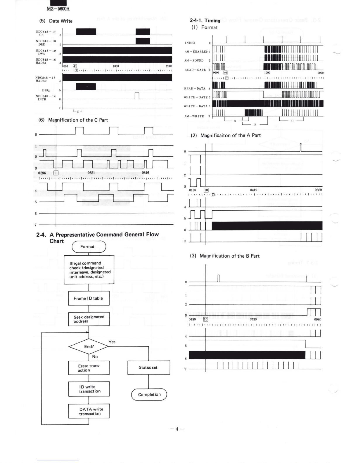
2-3. Basic Operations General Flow Chart
No
Power~n
or
reset
Command
control
program
format
,
read, write, seek,
etc
.
2-3-1.
Timing
(1) Command Transfer
NDC848-
17
CS
NDC848 - 18
DRD
NDC848 -
19
JJWR
NDC
848-
16
HADR1
NDC84
8-
15
HADRO
___
__
(hardware,
memory,
etc.}
2000
(2)
Magnification
of
the
A Part
-
MZ-5600A
.____
_
______.nL...__
_ ___,/L_
I I I I I I I I I
(3) Data
Read
NDC848 -
17
CS
NDC
848-
18
DRD
NDC848 - 19
DWI\
NDC848- 16
HADR1
I I I I
I I I I
1000
2000
I•
'''I
rl:l·· , ,
,,I,,
I'
•I
,,
''I'
I
''
I •
I'
I I I I ••
••••
'
I'
••
' I
NDC848 - 15
HADRO
DRQ
NDC848 - 14
INTR
(4)
Magnification
of
the B Part
0
--
-+--____J
3
0246
I 0271
0296
I•
I I I
,,
I I
[TI,
I I I I ' I I I I I I
••
I I I I I I I I I I I I I I I I I I I I I I I ' I I I I I I I I I I I I I I
5
6
------+-----------------------
----------------------
7
__
_,
____________
_______
___
- 3 -
-
MZ-5600A
(5) Data Write
NDC848-17
CS
NDC848-18
DRD
NDC848 -
19
OWR
NDC848 -
16
HADRI
NDC848 -
15
HADRO
DRQ
NDC848 -
14
INTR
(6) Magnification
of
the C Part
2-4. A Prepresentative Command General Flow
Chart
Illegal
command
check
(desi
gnated
interleave, designated
unit address,
etc
.)
- 4 -
2-4-1. Timing
(1) Format
INDEX
AM-
ENABLEO I
AM
- FOUND
READ-G
ATE
3
READ-
DATA
4
WRITE-G
ATES
WRITE-D
ATA
6
(2) Magnificaiton
of
the A Part
2
a
0169
[!Q]
04
19 0669
I I I I I I I I
•[T}
I I I I I I I I I I I I I I I I I I I I I I I I I I I I I I I I I I I I I I I I I
5
6
7
(3) Magnification
of
the 8 Part
o---+~nL_
__
__________
____
,L_
_
Ill
2
--+-
--------------~
"
~
3--
~--------
----
----------nll
0480
[!Q]
0700
0980
I'
I I I I ' I I I I I I I I
I•
I I I I I I I I I I I I I I I I I I J I I I I
I'
I'
I I I I
11
I
(4) Magnification
of
the
C Part
1
157
!.@]
1407
1
657
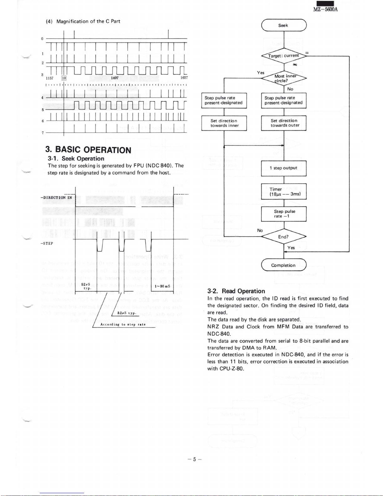
3.
BASIC OPERATION
3-1.
Seek
Operation
The
step
for
seeking
is
generated by FPU (NDC
840).
The
step
rate is designated by a
command
from
the
host.
- DIRECTION I N
-STEP
1-80
mS
L
A
ccordi ng l o llep
rat
e
- 5 -
Seek
1
step
output
3-2.
Read
Operation
-
MZ-5600A
In
the
read
operation, the
ID read
is
first
executed
to
find
the
designated
sector
. On finding
the
desired
ID
field,
data
are read.
The
data
read by
the
disk are
separated.
NRZ
Data
and
Clock
from
MFM Data
are
transferred
to
NDC-840.
The
data
are
converted
from serial
to 8-bit
parallel
and
are
transferred
by DMA
to
RAM.
Error
detection
is
executed
in NDC-
840
, and if
the
error
is
less
than
11
bits,
error
correction
is
executed
in association
with
CPU-Z-80.
b
-
MZ-5600A
Check
: illegal
command
, desig-
nated
unit
address, etc.
Sector
address + 1
No
No
1
step
seek
head =
0,
cylinder =
+1
Yes
- 6 -
READ
INDEX
AM-
ENABLEO I
AM-
FOlJND
READ-GA
TE 3
~
I
~
~
0000
:
rn
.. I··,. , .... , ... ,,
,,,,,,,
,,,,,,.,
..
,.,,,,,,
D
ATAO
DATA
l
L__A
___j
3
Magnification
of
the
A Part
I
I
I I
0
140
[Q]
'
0390
0640
, , . , . , ... , , m , , , , . , , , , , , , , , , , . , , , , , ,
..
, , , , , .. , , , ,
3-3. Write Operation
In
the
data
write
operation,
the
ID
read
is
first
executed
to
search
the
designated
sector
. On finding
the
desired
ID
field,
the
write
gate is
opened
and
writing
is
executed
.
Write
data
are
transferred
from
the
host
to
RAM,
then
from
RAM
to
NDC-840,
where
they
are
transformed
to
serial
data
. As
the
ECC
is
generated
by
the
ECC
Generator,
the
data
are
transformed
into
the
MFM
pattern
and
transferred
.._.,
to
the
disk.
After
completing
the
data, the
generated
ECC
(error
correcting
code)
is
transferred
to
the
disk.
No
No
No
-
Check : illegal
command,
designated unit
address, etc.
WR
IT E
I N
DEX
AM
- ENABLEO
AM
- FOUND
RE
AD-GATE
RE
AD-
DATA
WRITE-DATA
6
-
MZ-5600A
0000
~
I
000
2000
,,,
, , r
LrJ
,,,,,,,
r,, ,,,,,,,,,
' '
,,,,,,,,
'''
I•
•' ,,,, ,,,
'
l__
A
__j
Magnification
of
the A Part
0
--t----''
I
2
--~---~'----------
3
I
0117
0367
0617
, . , .. , , , , , , . , m, , . , , , .... , . , , . ,
..
, , , . ,
..
, .. , . , ,
..
, ,
- 7 -
-
MZ-5600A
4.
DRIVE INTERFACE
4-1. Drive Interface Signals
(1) Control Signal Interface Connector (CN1)
Pin
No.
signals Pin
No.
Signals
2 · · ·
REDUCED
WRITE
CURRENT
I
HEAD
SELECT
2
3
1
GND
GND
GND
GND
4
HEAD
SELECT2
2
3
6
8
10 ....
..
12 ...
.. .
14 .
.....
16 ......
18 ....
. .
20 ....
. .
22
....
..
24 ..... .
26
····
··
28
... ...
30 . . .
...
32 . .....
84
...
...
WRITE
GATE
SEEK
COMPLETE
TRACKO
WRITE
FAULT
HEAD
SELECT
2°
RESERVED
HEAD
SELECT
2
1
INDEX
READY
STEP
DRIVE
SELECT
1
DRIVE
SELECT
2
DRIVE
SELECT
3
DRIVE
SELECT
4
DIRECT
ION
IN
5
7
9 GND
11 ···
···
GND
13 ······ GND
15
·····
· GND
17 ·····
· GND
19
·····
· GND
21 ····· · GND
23 ·····
· GND
25
··
·· ··
GND
?:l ···
···
GND
29
···
···
GND
81 ······ GND
33
····· · GND
1
33
31
2}
'Zl
- - - - - - - • - - - - - -8
~
CN1
connector
designated
pin
No.
o o o o
--------------0
o I
0 0 0
0--------------0
0.
84
32
30
28
4 2
(2) Data Signal Interface Connector (CN2)
Pin No.
Signals
Pin No .
Signals
2 GND
1 .
..
DRIVE
SELECTED
4
GND 3
RESERVED
6 GND
5
SPARE
8 GND 7
RESERVED
10
......
SPARE
9
SPARE
12 ......
GND
11
......
GND
14
...
-MFM
WRITE
DATA
13 ... +MFM
WRITE
DATA
16
..
..
..
GND
15
.. · ..
· GND
18 ...
-MFM
READ DATA
17 ...
+MFM
READ
DATA
20 ....
..
GND
CN2 connector
designated
pin
No .
t
19
......
GND
19
17
15
- - - - - - - 3
ODD
--------o
ODD
--------0
20 1816 - - - - - - - 4 2
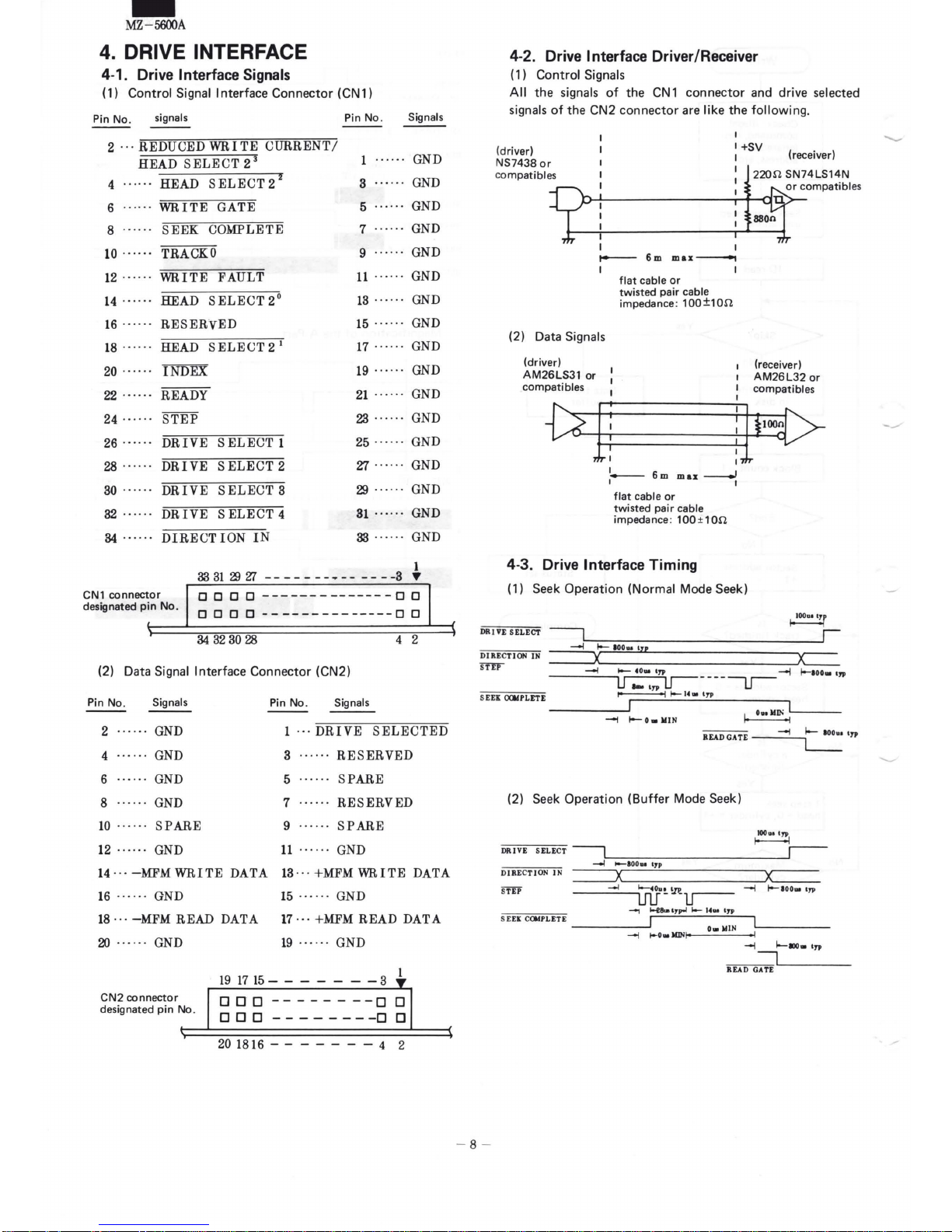
4-2. Drive Interface Driver/Receiver
( 1) Control Signals
All
the signals
of
the
CN1
connector and drive selected
signals
of
the CN2 connector
are
like the
following
.
I
(driver)
NS7438
or
compatibles
I +SV
I
(receiver)
I
t---
6m
max--,
I I
(2) Data Signals
(driver)
AM26LS31
or
:
compatibles
I
flat
cable
or
twisted pair cable
impedance:
100±10.n
-
I
6m
max---'
I
flat
cable
or
twisted pair cable
impedance: 100±10.n
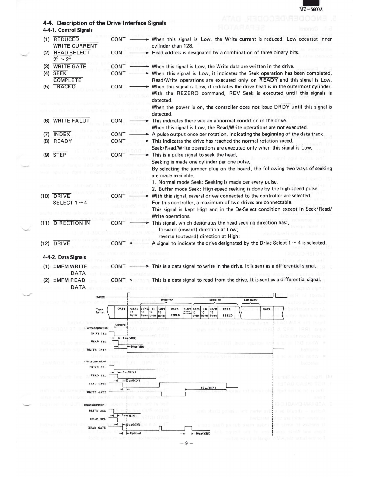
4-3. Drive Interface Timing
(1) Seek Operation (Normal Mode Seek)
(receiver)
AM26L32
or
compatibles
DRIVE
SELECT
DIRE
CTION IN
S'fEP
~
I--
IOOu trp
--~X
~
--1
-
eo
..
'"
--1
1-aoo.
,,
~----~
:-;S E""
EJ[
;;;-
OCAI=P=-:L-=:ET=E
~
IC,. 1n>
--i
-O•JoiiN
--:REA_D_G-AT-E
~In>
(2)
Seek
Operation
(Buffer
Mode Seek)
DRIVE SELECT
--l
1--IOOu
trp
DIRECTION IN
=:J~;----------,-'X'----
_
--~;.;__
......
Ouo
!n.
-l
~
lOO•
In>
UlJ-
~
.....,
~--ta-t,.poo~
t--
14u.
'"
S
EU
C<»>PLETE
____
....J
-~·~·~Joi~IN~~L------
-l
t-O•MINI--
-1
l-IDO•
In>
I
READ
GATE.__
___
_
- 8 -
-
----
-
MZ-5600A
4-4. Description
of
the Drive Interface
Signals
4-4-1. Control Signals
( 1)
REDUCED
WRITE
CURRENT
(2)
HEAD
SELECT
2?-
2
2
(3)
WRITE GATE
(4)
SEEK
COMPLETE
(5)
TRACKO
(6)
WRITE
FALUT
(7)
INDEX
(8)
READY
(9)
STEP
(10) DRIVE
SELECT1
- 4
(11)
DIRECTIONIN
(12) DRIVE
4-4-2. Data Signals
(1)
±MFMWRITE
DATA
(2)
±MFM
READ
DATA
CONT
CONT
CONT
CONT
CONT
CONT
CONT
CONT
CONT
CONT
CONT
CONT
CONT
CONT
When
this
signal is Low,
the
Write
current
is
reduced.
Low
occursat
inner
cylinder
than 128
.
Head address
is
designated
by a combination
of
three
binary
bits.
When
this
signal
is
Low,
the
Write
data
are
written
in
the
drive.
When
this sign
al
is Low ,
it
indicates
the
Seek
operation
has
been
completed
.
Read/Write
ope
rati
ons
are
executed
only
on
READY
and
this signal
is
Low.
When this sign
al
is
Low, it indicates
the
drive head
is
in
the
outermost
cylinder.
With
the
REZERO
command, REV
Seek
is
executed
until
this
signals
is
detected
.
When
the
power is on,
the
controller
does
not
issue
DRDY
until
this
signal
is
detected.
This
indicate
s there was an
abnormal
condition
in
the
drive.
When
this
signal
is
Low,
the
Read/Write
operations
are
not
executed.
A pulse
output once
per
rotation,
indicating
the
beginning
of
the
data
track.
This
indicates the
drive has reached
the
normal
rotation
speed.
Seek/Read/Write
operations
are
executed
only
when
this
signal
is
Low.
This
is
a pulse signal
to
seek
the
head.
Seeking
is
made
one
cylinder
per
one
pulse.
By
selecting the j
umper
plug on
the
board, the
following
two
ways
of
seeking
are
made
available .
1. Normal
mode
Seek
: Seeking
is
made
per
every pulse.
2. Buffer
mode
Seek: High -
speed
seeking
is
done
by
the
high-speed pulse.
With
this
signa
l,
several drives
connected
to
the
controller
are
selected
.
For
this
controller, a
maximum
of
two
drives are
connectable
.
This signal
is kep
t High
and
in
the De-
Select
condition
except
in
Seek/Read/
Write
operat
ions.
---
This signal, which designates
the
head seeking
direction
has:,
forward
(inward)
direction
at
Low;
reverse
(outward)
direction
at
High;
A signal
to
indicat e
the
drive
designated
by
the
Drive
Select
1 - 4
is
selected
.
This
is a data
signal
to
write
in
the
drive.
lt
is
sent
as a differential signal.
This
is a data
signal
to
read
from
the
drive.
lt
is
sent
as a differential
signal.
IN
DEX
----!
'-------....,.,...-
---
----,----------.1
Sector
00
Sector
01
l
•t
aector
,-,-~--~=;~==~==~~~~~;===~~----'~~~
~~
___l____..l._~
__L____._l__l(
I Gm I (
Track
format
{Fo
i1'N
t operet ion)
1
0ptione
l~
:
DR
IT E S E L
HEAD
SEL
WR
ITE OA
TE
{W
rite
o~tion
)
DRIVE
SEL
BEAD
SEL
'
'
'
--f
.._O
.. (lUN
)
!i
--t
1-&0u•(lO
N)
--t
t-50u•OHN)
READ GA
TE
~~+
:
____
__J
WRITE OATE
__
-4-'--Tt---
----,
I
Reed
operation)
DRIVE S
EL
---,
:
-t
t-
Oua,(MJN)
IIEADSEL
~
-+1
,._50u•(W:IN
)
8
0-..
(MIN)
READ GATE
~
L..;..:
____
__.JnL. ___
..JnL
_ _ _
-t
;..._
Optional
---t
1-
80
Ul
(
)f]N
)
- 9 -
-
MZ-5600A
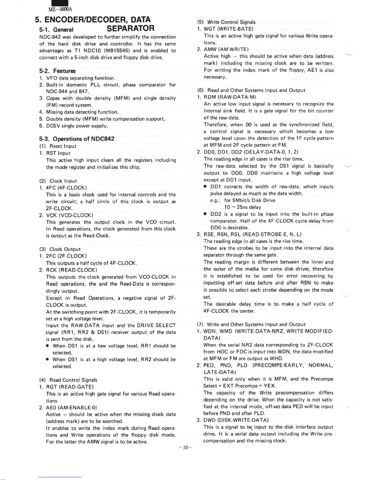
5. ENCODER/DECODER,
DATA
5-1.
General
SEPARATOR
NDC-842 was
developed
to
further
simplify
the
connection
of
the
hard
disk drive
and
controller. it
has
the
same
advantages as
T1
NDC10
(MB15546)
and
is
enabled
to
connect
with
a 5 -inch disk drive
and
floppy
disk drive.
5-2.
Features
1.
VFO
data
separating
function.
2. Built-in
domestic
PLL
circuit,
phase
comparator
for
N DC-844
and
84
7.
3.
Copes wi
th
double
density
(MFM)
and
single
density
(FM)
record
system.
4. Missing
data
detecting
function
.
5.
Double
density
(MFM)
write
compensation
support
.
6.
DC5V single
power
supply.
5-3. Operations
of
NDC842
(1) Reset
Input
1.
RST
Input
This active high
input
clears
all
the
registers including
the
mode
register and initializes
this
chip.
(2)
Clock
Input
1.
4FC
(4F-CLOCK)
This
is
a basic
clock
used
for
internal
controls
and
the
write
circuit; a half
circle
of
this
clock
is
output
as
2F-CLOCK .
2. VCK (VCO-CLOCK)
This
generates
the
output
clock
in
the
VCO
circuit
.
In Read
operations,
the
clock
generated
from
this
clock
is
output
as
the
Read-Clock.
(3) Clock
Output
1.
2FC
(2F-CLOCK)
This
outputs
a half
cycle
of
4F-CLOCK.
2. RCK (READ-CLOCK)
This
outputs
the
clock
generated
from
VCO-CLOCK in
Read
operations,
the
and
the
Read-Data
is
correspon
-
dingly
output
.
Except
in Read
Operations,
a negative signal
of
2F-
CLOCK
is
output.
At
the
switching
point
with 2F-CLOCK, it
is
temporarily
set
at
a high voltage level.
Input
the
RAW-DATA
input
and
the
DRIVE
SELECT
signal
(RR1,
RR2
& DS1) receiver
output
of
the
data
is
sent
from
the
disk.
• When
DS1
is
at
a low voltage level , R R 1
should
be
selected.
•
When
DS 1 is
at
a high voltage level, R R2
should
be
selected.
(4) Read
Control
Signals
1.
RGT
(READ-GATE)
This
is
an active high gate signal
for
various Read
opera-
tions
.
2. AEO (AM-ENABLE-D)
Active -
should
be active
when
the
missing
clock
data
(address
mark)
are
to
be
searched
.
it
enables
to
write
the
index
mark
during
Read
opera
-
tions
and
Write
operations
of
the
floppy
disk
mode.
For
the
latter
the
AMW signal
is
to
be active.
-10-
(5) Write
Control
Signals
1. WGT (WRITE -BATE)
This
is
an active high gate signal
for
various Write opera-
tions
.
2. AMW
(AM-WRITE)
Active high - this
should
be active
when
data
(address
mark)
including
the
missing
clock
are
to
be
written
.
For
writing
the
index
mark
of
the
floppy,
AE1
is
also
necessary.
(6) Read
and
Other
Systems
Input
and
Output
1. RDM (RAW-DATA-M)
An
active low
input
signal
is
necessary
to
recognize
the
internal sink field.
it
is
a gate signal
for
the
bit
counter
of
the
raw-
data
.
Therefore,
when
00
is
used
as
the
synchronized
field,
a
control
signal
is
necessary
which
becomes
a low
voltage level
upon
the
detection
of
the
1 F
cycle
pattern
at M FM
and
2 F cycle
pattern
at
FM.
2. DDO, DD1,
DD2
(DELAY-DATA-0, 1, 2)
The
reading edge in all cases
is
the
rise
time.
The
raw-data
selected
by
the
DS1
signal
is
basically
output
to
DDO. DDO
maintains
a high voltage level
except
at
DD1
input
.
• DD1
corrects
the
width
of
raw-data,
which
inputs
pulse
delayed
as
much
as
the
data width.
e.g.:
for
5Mbit/s
Disk Drive
10-
25ns
delay
•
DD2
is
a signal
to
be
input
into
the
built
-in phase
comparator.
Half
of
the 4F-CLOCK
cycle
delay
from
DDO
is
desirable.
3.
RSE, RSN , RSL (READ-STROBE-E,
N,
L)
The
reading edge in all cases
is
the
rise
time
.
These
are
the
strobes
to
be
input
into
the
internal
data
separator
through
the
same
gate.
The
reading margin
is
different
between
the
inner
and
the
outer
of
the
media
for
some
disk drives,
therefore
it
is
established
to
be used
for
error
recovering
by
inputting
off-set
data
before
and
after
RSN
to
make
it possible
to
select
each
strobe
depending
on
the
mode
set.
The
desirable delay
time
is
to
make a half
cycle
of
4F-CLOCK
the
center.
(7) Write and
Other
Systems
Input
and
Output
1. WDN, WMD (WRITE-DATA-NRZ, WRITE-
MODIFIED
DATA)
When
the
serial N R2
data
corresponding
to
ZF-CLOCK
from
HOC
or
FDC
is
input
into
WDN ,
the
data
modified
at
MFM
or
FM are
output
as WHD.
2.
PED, PND, PLD
(PRECOMPE-EARLY
, NORMAL,
LATE-DATA)
This
is
valid
only
when
it
is
MFM,
and
the
Precompe
Select=
EXT
Precompe
= YEX.
The
capacity
of
the
Write
precompensation
differs
depending
on
the
drive. When
the
capacity
is
not
satis-
fied
at
the
internal
mode,
off-set
data
PED will be
input
before
PND
and
after
PLD .
3.
DWD (DISK-WRITE-DATA)
This
is
a signal
to
b~
input
to
the
disk
interface
output
drive.
it
is
a serial
data
output
including
the
Write
pre
compensation
and
the
missing
clock
.
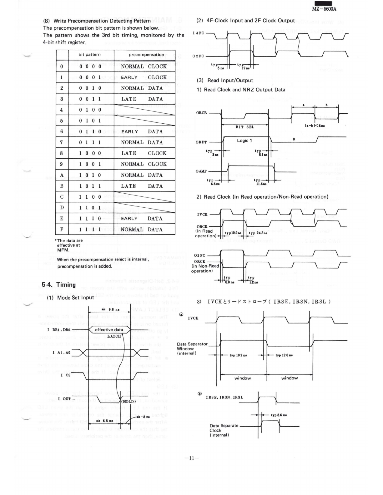
(8) Write Precompensation Detecting Pattern
The precompensation
bit
pattern
is
shown below.
(2) 4F-Ciock
Input
and 2F Clock
Output
-
MZ-5600A
The pattern shows the 3rd
bit
timing,
monitored by the
4-
bit
shift
register.
bit
pattern
0 0
1
0
2
0
3
0
4 0
5
0
6
0
7
0
8
1
9
1
A
1
B
1
c 1
D
1
E 1
F
1
*Th
e data are
effective
at
MFM
.
0 0 0
0 0
1
0
1 0
0
1
1
1
0 0
1 0 1
1 1
0
1 1
1
0 0 0
0
0 1
0 1 0
0
1
1
1
0
0
1
0
1
1
1
0
1 1 1
precompensation
NORMAL
CLOCK
EARLY
CLOCK
NORMAL
DATA
LATE
DATA
-----
-------
EARLY
DATA
NORMAL
DATA
LATE
CLOCK
NORMAL
CLOCK
NORMAL
DATA
LATE
DATA
----
-----
EARLY
DATA
NORMAL
DATA
When
the
precompensation select is
internal,
precompensation
is
added.
5-4. Timing
(
1)
Mode Set
Input
oil 9.8
no
I
AI,
AO
I
CS
'----JI(HOLD)
·
·-8
Dl
oil 6.8
Dl
(3)
Read
Input/Output
1)
Read
Clock and N RZ
Output
Data
•
b
ORCR
~
I
v---
BIT
SEL
lo-b
I<&DO
logic
1
0
I
-
ORDT
yp-
~
lyp-
1--
8DO
8.101
OAMF
7P
lyp
&.&no
11.6no
2)
Read
Clock (in
Read
operation/Non-
Read
operation)
02
FC
~
~
r
\'----------.1/
~
ORCK
r---~
(in
Non
-Read
--+1
\.._
__
.-~/
\'----'
operation)
lyp
lyp
6.8
DO
1.2no
3)
I V
CK
c
')
-
f:
.7.
I-
o - 7 ( I R
SE
, I R S
N,
I R S L )
IVCK
--J
Data Separate
Window
(interna
l)
r_
\
lyp 10.7
Dl
window
I
RSE,
IRSN.
IRSL
--
- - lyp
12.6
DO
window
.I
\.
----if-+--
lyp 8.8 DO
-11-
Data Separate
---l..IJ
Clock
(internal)
\
I
-
MZ-5600A
(4) Write
Input/Output
1)
Write Clock
and N RZ
Input
Data
14
FC
0
2F
C
Write Clock
2) MFM Data
OWMD
Data
Bit
Clock
Bit
DWD
Output
(1)
Write
M
in8n
::s
M
in
4 n s
Precompensation
Data
··
..................
........
..... Precompensation Mode
*Early
Data
*Normal
Data
*Late
Data
* Early,
Normal,
Late-
Same
with
Clock
Bit
DWD
Output
2 . . . . . . . . Precompensation Mode at
EXT
IPED
IPND
---..J
I
!PLO
ODWD
6.
MAINTENANCE (Trouble-ihooting)
6-1. Genral
Trouble analysis
of
the NDC5801 Hard Disk Controller
is
described, sequence by sequence.
6-2. Tools
The tools necessary
for
trouble analysis
are
the
following
.
(1) Host system (MZ-6500)
(2) Troubled
5"
Disk and NDC5801 controller
(3) Oscilloscope
(4) Test program
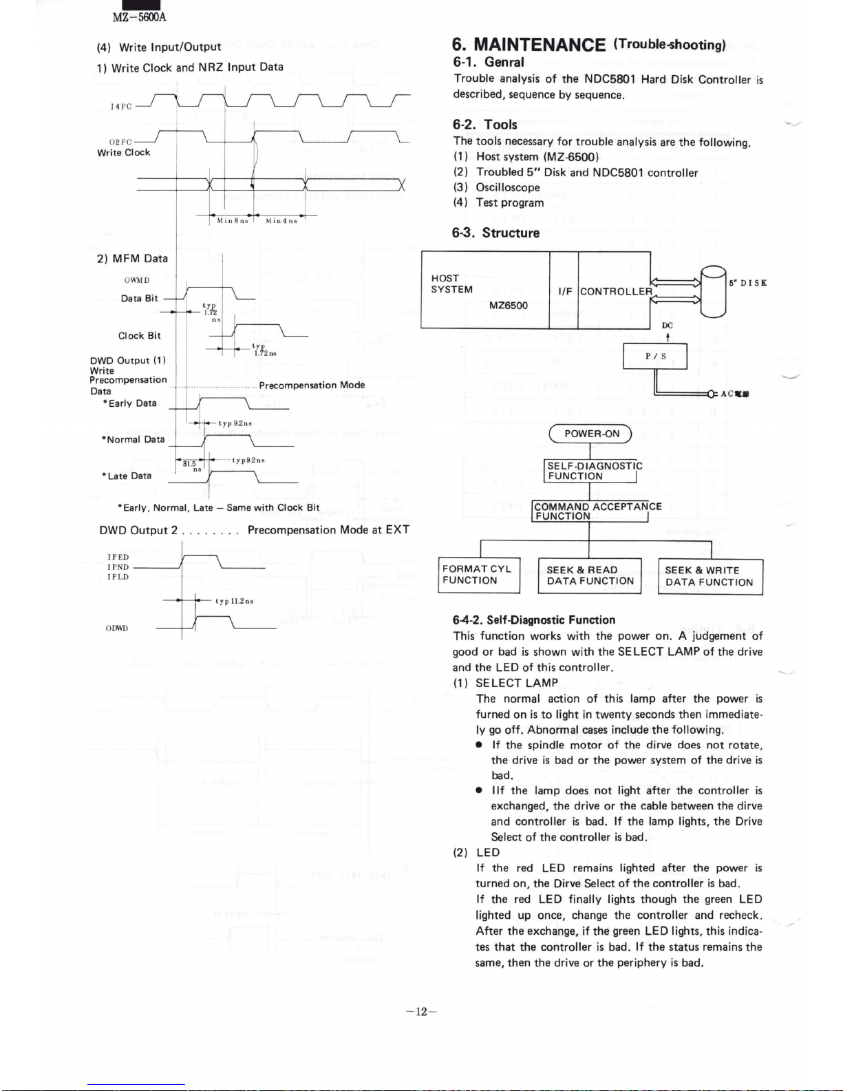
6-3. Structure
I
r---
HOST
r------
SYSTEM
1/F
CONTROLLER
6"
D l S K
MZ6500
I
DC
6-4-2. Self-Diagnostic Function
This
function
works
with
the power on. A judgement
of
good
or
bad
is
shown
with
the SELECT LAMP
of
the drive
and the LED
of
this controller.
(1) SELECT LAMP
The
normal action
of
this lamp after the power
is
turned on
is
to
light in
twenty
seconds
then immediate·
ly
go
off.
Abnormal
cases
include the following.
•
If
the spindle
motor
of
the dirve
does
not
rotate,
the drive
is
bad
or
the power system
of
the drive
is
bad.
•
llf
the lamp
does
not
light after the controller
is
exchanged, the drive
or
the cable between the dirve
and
controller
is
bad.
If
the lamp lights, the Drive
Select
of
the controller
is
bad.
(2) LED
If
the red LED remains lighted after the power
is
turned on, the Dirve Select
of
the controller
is
bad.
If
the red LED
finally
lights though the
green
LED
lighted up once, change the controller and recheck.
After
the exchange,
if
the
green
LED lights, this indica-
tes
that
the controller
is
bad.
If
the status remains the
same,
then the drive or the periphery
is
bad
.
-12-
 Loading...