

Page 1
SERVICE MANUAL
Ver 1.1 2004. 09
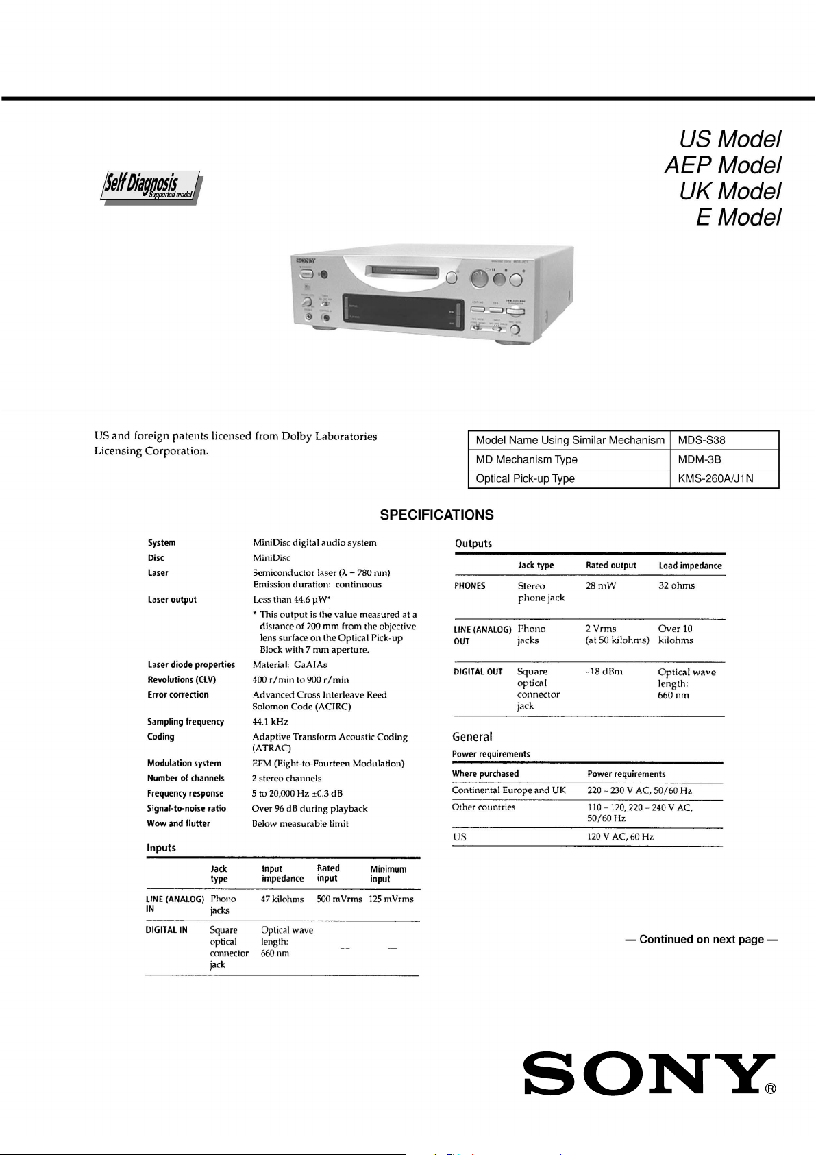
MDS-PC1
9-922-739-13
2004I02-1
© 2004.09
MiNi DiSC DECK
Sony Corporation
Audio Group
Published by Sony Engineering Corporaton
Page 2
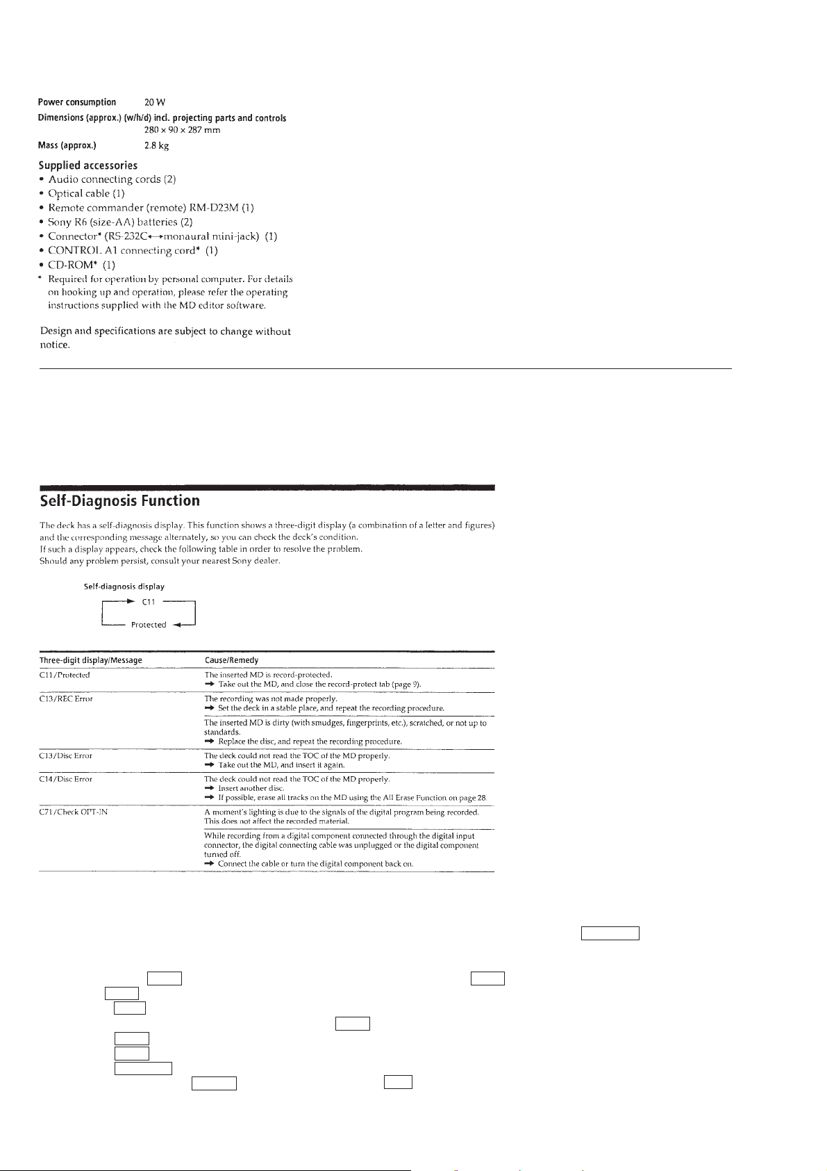
SELF-DIAGNOSIS FUNCTION
The self-diagnosis function consists of error codes for users which are displayed automatically when errors occur, and error codes which
show the error history in the test mode during servicing. For details on how to view error codes for users, refer to the following box in the
instruction manual. For details on how to perform checks during servicing, refer to the following “Procedure for Using the Self-Diagnosis
Function (Error History Display Mode)”.
Procedure for Using the Self-Diagnosis Function (Error History Display Mode)
Note: Perform the self-diagnosis function in the “error history display mode” in the test mode. The following describes the least required
steps. Be careful not to enter other modes by mistake. If other modes are set accidentally, press the EDIT/NO button to exit that
mode.
1. While pressing the AMS dial, connect the power plug to the outlet, and release the AMS dial.
2. Rotate the AMS dial until “ERR DP MODE” is displayed.
3. Pressing the YES button sets the error history mode and displays “total rec”.
4. Select the contents to be displayed or executed using the AMS dial.
5. Pressing the AMS dial displays or executes the contents selected.
6. Pressing the AMS dial another time returns to step 4.
7. Pressing the EDIT/NO button displays “ERR DP MODE” and exits the error history mode.
8. T o e xit the test mode, set the TIMER knob to “OFF”, and press the 1/u button. The unit sets into the STANDBY state, and the test mode
ends.
– 2 –
Page 3
ITEMS OF ERROR HISTORY MODE ITEMS AND CONTENTS
Selecting the Test Mode
Display
total rec
total play
retry err
total err
err history
er refresh?
Details of History
Displays the recording time in the form of “rππππππh”.
The displayed time is the total number of hours the laser is high power, which is about one-fourth of the actual
recording time. The time is displayed in decimal digits between 0h and 65535h.
Displays the playback time in the form of “pππππππh”.
The displayed time is the total actual play time. The paused time is not counted. The time is displayed in decimal
digits between 0h and 65535h.
Displays the total number of retries during recording and retry errors during playback in the form of “rππpππ”.
r indicates the retries during recording while p indicates the retry errors during playback. The number of retries is
displayed in hexadecimal digits between 00 and FF.
Displays the total number of errors in the form of “totalππ”.
The number of errors is displayed in hexadecimal digits between 00 and FF.
Displays the 10 latest errors in the form of “0π E@@”.
The π indicates the history number. The smaller the number, the newer is the error. (00 is the latest error.)
The @@ indicates the error code. Refer to the following table for details. Rotate the AMS dial to switch the error
history.
Mode which erases all the error histories.
The error history serves as a reference for when to replace the optical pick-up. Perform this procedure when the
optical pick-up has been replaced in order to erase past error histories and not at other times. Press the YES button
when “er refresh??” is displayed. The history will be erased and “Complete!” will be displayed momentarily. Be
sure to check the following when this mode has been executed.
*Check that the data has been erased.
*Perform recording and playback, and check that the mechanism operates normally.
Table of Error Codes
Error Code
E00
E01
E02
E03
E04
No error
Disc error. Cannot read PTOC
(Disc is ejected out)
Disc error. UTOC error
(Disc is not ejected out)
Loading error
Cannot read address (Servo has deviated)
Details of Error
Error Code
E05
E06
E07
E08
E09
E0A
Details of Error
FOK has deviated
Unfocused (Servo has deviated)
Recording retry
Recording retry error
Play retry error
(Access error)
Playback retry error (C2 error)
– 3 –
Page 4
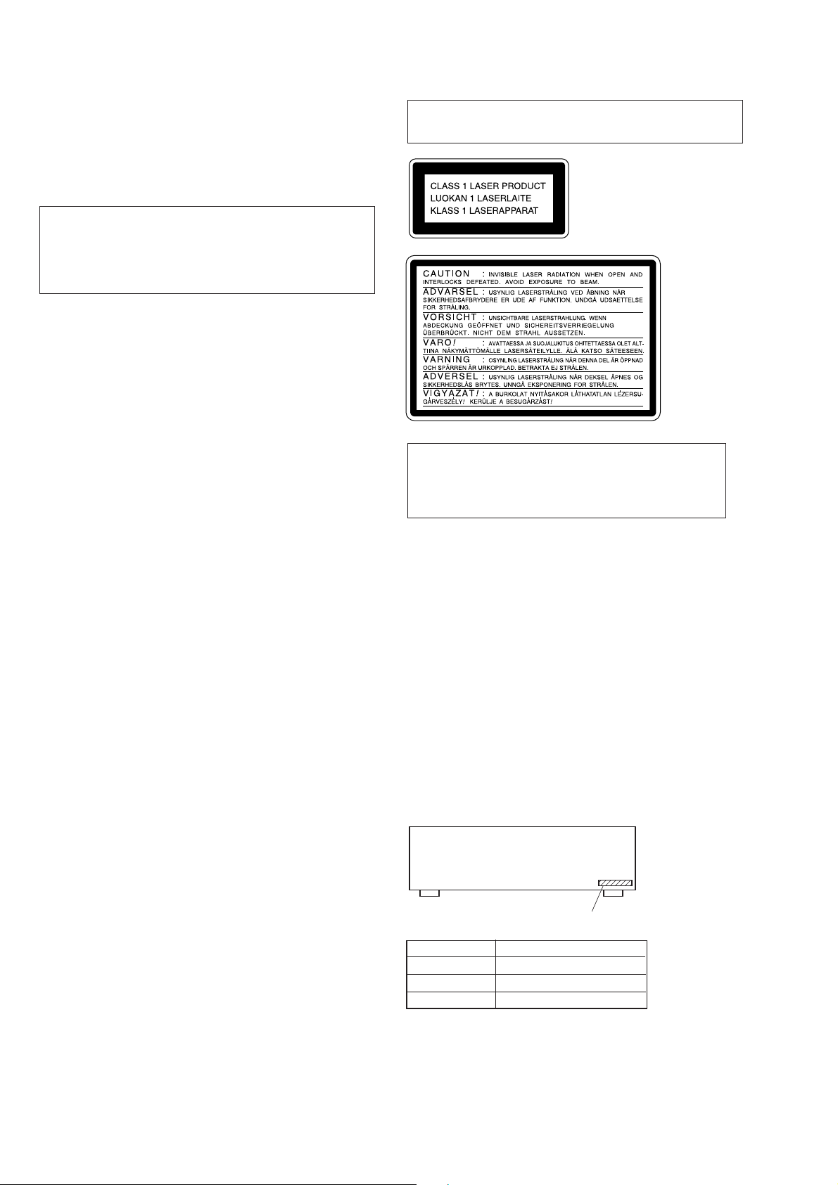
CAUTION
Danger of explosion if battery is incorrectly replaced.
Replace only with the same or equivalent type recommended by
the equipment manufacturer.
Discard used batteries according to manufacture’s instructions.
ADVARSEL!
Laser component in this product is capable of emitting radiation
exceeding the limit for Class 1.
This appliance is classified as
a CLASS 1 LASER product.
The CLASS 1 LASER PRODUCT MARKING is located on
the rear exterior.
Lithiumbatteri - Eksplosionsfare ved fejlagtig håndtering.
Udskiftning må kun ske med batteri af samme fabrikat og type.
Levér det brugte batteri tilbage til leverandøren.
ADVARSEL
Eksplosjonsfare ved feilakting skifte av batteri.
Benytt samme batteritype eller en tilsvarende type anbefalt av
apparatfabrikanten.
Brukte batterier katterier kasseres i henhold til fabrikantens
VARNIG
Explosionsfara vid felaktigt batteribyte.
Använd samma batterityp eller en likvärdig typ som rekommenderas
av apparattillverkaren.
Kassera använt batteri enligt gällande föreakrifter.
VAROITUS
Parist voi räjähtää, jos se on virheellisesti asennettu.
V aihda paristo ainoastaan laite valmistajan suosittelemaan tyyppiin.
Hävitä käytetty paristo valmistajan ohjeiden mukaisesti.
This caution
label is located
inside the unit.
CAUTION
Use of controls or adjustments or performance of procedures
other than those specified herein may result in hazardous radiation exposure.
Notes on chip component replacement
• Never reuse a disconnected chip component.
• Notice that the minus side of a tantalum capacitor may be
damaged by heat.
Flexible Circuit Board Repairing
• Keep the temperature of soldering iron around 270˚C
during repairing.
• Do not touch the soldering iron on the same conductor of the
circuit board (within 3 times).
• Be careful not to apply force on the conductor when soldering
or unsoldering.
SAFETY-RELATED COMPONENT WARNING !!
COMPONENTS IDENTIFIED BY MARK ! OR DO TTED LINE
WITH MARK ! ON THE SCHEMATIC DIAGRAMS AND IN
THE PARTS LIST ARE CRITICAL TO SAFE OPERATION.
REPLACE THESE COMPONENTS WITH SONY PARTS
WHOSE PART NUMBERS APPEAR AS SHOWN IN THIS
MANUAL OR IN SUPPLEMENTS PUBLISHED BY SONY.
MODEL IDENTIFICATION
— BACK PANEL —
Parts No.
PARTS No. MODEL
4-996-315-1π Singapore model
4-996-315-2π AEP, UK model
4-996-315-3π US model
– 4 –
Page 5
SAFETY CHECK-OUT
TABLE OF CONTENTS
After correcting the original service problem, perform the following safety checks before releasing the set to the customer:
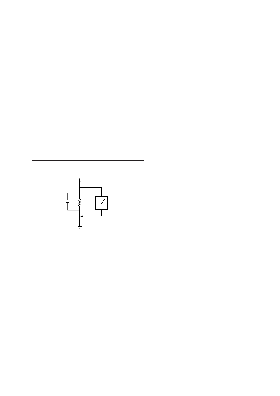
Check the antenna terminals, metal trim, “metallized” knobs, screws,
and all other exposed metal parts for AC leaka ge. Check leakage as
described below.
LEAKAGE
The AC leakage from any exposed metal part to earth Ground and
from all exposed metal parts to any exposed metal part having a
return to chassis, must not exceed 0.5 mA (500 microampers). Leakage current can be measured by any one of three methods.
1. A commercial leakage tester, such as the Simpson 229 or RCA
WT-540A. Follow the manufacturers’ instructions to use these
instruments.
2. A battery-operated AC milliammeter. The Data Precision 245
digital multimeter is suitable for this job.
3. Measuring the voltage drop across a resistor by means of a V OM
or battery-operated A C v oltmeter. The “limit” indication is 0.75
V, so analog meters must have an accurate low-voltage scale.
The Simpson 250 and Sanwa SH-63Trd are examples of a passive VOM that is suitable. Nearly all battery operated digital
multimeters that have a 2V AC range are suitable. (See Fig. A)
To Exposed Metal
Parts on Set
0.15µF
1.5k
Ω
AC
voltmeter
(0.75V)
1. SERVICING NOTE .......................................................... 6
2. GENERAL .......................................................................... 9
3. DISASSEMBLY
3-1. Front Panel ......................................................................... 29
3-2. Back Panel and Main Board ...............................................30
3-3. Bracket (T)/(L)/(R) ............................................................. 31
3-4. SUB Chassis ....................................................................... 31
3-5. Shutter Assembly ................................................................ 32
3-6. Slider Complete Assembly.................................................. 33
4. TEST MODE ..................................................................... 34
5. ELECTRICAL ADJUSTMENTS ............................... 38
6. DIAGRAMS
6-1. Circuit Boards Location ...................................................... 43
6-2. Block Diagrams
• BD Section ....................................................................... 45
• Main Section ....................................................................47
6-3. Schematic Diagram – BD (1/2) Section –........................... 51
6-4. Schematic Diagram – BD (2/2) Section –........................... 53
6-5. Printed Wiring Board – BD Section –.................................55
6-6. Printed Wiring Board – SW Section – ................................57
6-7. Schematic Diagram – SW Section – ................................... 58
6-8. Printed Wiring Board – Main Section –.............................. 59
6-9. Schematic Diagram – Main (1/3) Section – ........................ 61
6-10. Schematic Diagram – Main (2/3) Section – ...................... 63
6-11. Schematic Diagram – Main (3/3) Section – ...................... 65
6-12. Printed Wiring Board – Panel Section –............................ 67
6-13. Schematic Diagram – Panel Section – .............................. 69
6-14. IC Block Diagrams ........................................................... 71
6-15. IC Pin Functions ............................................................... 76
Earth Ground
Fig. A. Using an AC voltmeter to check AC leakage.
7. EXPLODED VIEWS
7-1. Front Panel Section ............................................................. 84
7-2. Chassis Section ................................................................... 85
7-3. Mechanism Deck Section 1 (MDM-3B) .............................86
7-4. Mechanism Deck Section 2 (MDM-3B) .............................87
8. ELECTRICAL PARTS LIST ........................................ 88
– 5 –
Page 6
SECTION 1
SERVICING NOTE
BD BOARD WAVEFORM CHECK TOOL
Use the jig (J-2501-124-A or J-2501-149-A) to facilitate the checking of the waveform of the BD board. The names and check items of each
terminal are as follows.
I+3V : For measuring the IOP (check if the optical pick-up laser has weakened)
IOP : For measuring IOP (check if the optical pick-up laser has weakened)
TEO : TRK error signal (traverse adjustment)
VC : Reference level for checking signals
RF : RF signal (jitter check)
Mechanism deck
Jig
RF
RF
VC
TEO
IOP
I+3V
GND
CN110
6P connector
Jig
(J-2501-149A)
GND can not be used.
H-3V
IOP
TEO
VC
(J-2501-124A)
[FORCED RESET]
Perform forced reset if the unit does not operate normally due to the hangup of the microprocessor.
It is recommended that this be performed when the test mode and retry cause display mode cannot be exited, or when the unit does not
operate normally when reassembled after being disassembled.
Method:Disconnect the power plug from the outlet, short-circuit the JW143 and 164 (RESET) of the MAIN board using a pair of tweezers,
and discharge the backup battery.
[MAIN BOARD] (Component Side)
JW143 JW164
CN307
IC401
IC101
– 6 –
Page 7
RETRY CAUSE DISPLAY MODE
* In this test mode, the causes for retry of the unit during recording and stop can be displayed on the fluorescent display tube. During
playback, the “track mode” for obtaining track information will be set.
This is useful for locating the faulty part of the unit.
* The following will be displayed:
During recording and stop :Retry cause, number of retries, and number of retry errors.
During playback :Information such as type of disc played, part played, copyright.
These are displayed in hexadecimal.
Procedure:
1. Load a recordable disc whose contents can be erased into the unit.
2. Press the MENU/NO button. When “Edit Menu” is displayed on the fluorescent display tube, rotate the AMS dial to display “All
Erase?”.
3. Press the YES button. (Or press the AMS dial)
4. When “All Erase??” is displayed on the fluorescent display tube, the music calendar number blinks.
5. Press the YES button to displa y “Complete!!”, and press the p button immediately . Wait for about 15 seconds while pressing the button.
(The AMS dial can be pressed instead of the YES button for the same results.)
6. When the “TOC” displayed on the fluorescent display tube goes off, release the p button.
7. Press the rREC button to set the recording standby state. Then press the ·P button to start recording.
8. Press the DISPLAY/CHAR button and check the test mode display (Fig. 1).
9. T o c heck the “track mode”, press the ·P button to start play. Then press the DISPLAY/CHAR button to display the test mode display
(Fig. 2), and check the display.
10. T o exit the test mode, press the 1/u button to turn OFF the power. When “TOC” disappears, disconnect the po wer plug from the outlet.
If the test mode cannot be exited, refer to “Forced Reset” on page 5.
Fig. 1 Reading the Test Mode Display (During recording and stop)
RTs@@c##e**
Fluorescent display tube display
@@: Cause of retry
## : Number of retries
** : Number of retry errors
Fig. 2 Reading the Test Mode Display (During playback)
@@####** $$
Fluorescent display tube display
@@: Parts No. (name of area named on TOC)
## : Cluster
** : Sector
$$ : Track mode (Track information such as copyright information of each part)
Reading the Retry Cause Display
Hexadecimal
Bit
Binary
Address (Physical address on disc)
}
Higher Bits Lower Bits
84218421
b7 b6 b5 b4 b3 b2 b1 b0
00000001
00000010
00000100
00001000
00010000
00100000
01000000
10000000
Hexa-
decimal
01
02
04
08
10
20
40
80
Cause of Retry Occurring conditions
shock
Discontinuous address
ader5
DIN unlock
FCS incorrect
IVR rec error
CLV unlock
Access fault
When track jump (shock) is detected
When ADIP address is not continuous
When ADER was counted more than five times
continuously
When DIN unlock is detected
When not in focus
When ABCD signal level exceeds the specified range
When CLV is unlocked
When access operation is not performed normally
– 7 –
Page 8
Reading the Display:
Convert the hexadecimal display into the binary display. If more than two causes, they will be added.
Example
When 44 is displayed:
Upper bit : 4=0100 n b6
Lower bit : 4=0010 n b2
In this case, the retry cause is combined of “CVL unlock” and “ader5”.
When A4 is displayed:
Upper bit : A=1010 n b7+b5
Lower bit : 4=0010 n b2
The retry cause in this case is combined of “access fault”, “IVR rec error”, and “ader5”.
Reading the Track Mode Display
Higher Bits Lower Bits
Hexadecimal
Bit
Binary
Reading the Display:
Convert the hexadecimal display into the binary display. Several cause are added and displayed.
Example
When 84 is displayed:
Upper bit : 8=1000 n b7
Lower bit : 4=0100 n b2
In this case, as b2 and b7 are 1 and others are 0, the cause is combined of “Emphasis OFF”, “Monaural”, “Original”, Copyrighted” and
“Write permitted”.
When 07 is displayed:
Upper bit : 0=0000 n all 0
Lower bit : 7=0111 n b0+b1+b2
In this case, as b0, b1, and b2 are 1 and others are 0, the cause is combined of “Emphasis ON”, “Stereo”, “Original”, Copyrighted” and
“Write prohibited”.
84218421
b7 b6 b5 b4 b3 b2 b1 b0
00000001
00000010
00000100
00001000
00010000
00100000
01000000
10000000
Hexa-
decimal
01
02
04
08
10
20
40
80
When 0 When 1
Emphasis OFF
Monaural
This is 2-bit display. Normally 01.
01:Normal audio. Others:Invalid
Audio (Normal)
Original
Copyright
Write prohibited
Details
Emphasis ON
Stereo
Invalid
Digital copy
No copyright
Write allowed
Hexadecimal/Decimal Conversion Table
Hexadecimal Binary Hexadecimal Binary
0
1
2
3
4
5
6
7
0000
0001
0010
0011
0100
0101
0110
0111
8
9
A
B
C
D
E
F
1000
1001
1010
1011
1100
1101
1110
1111
– 8 –
Page 9
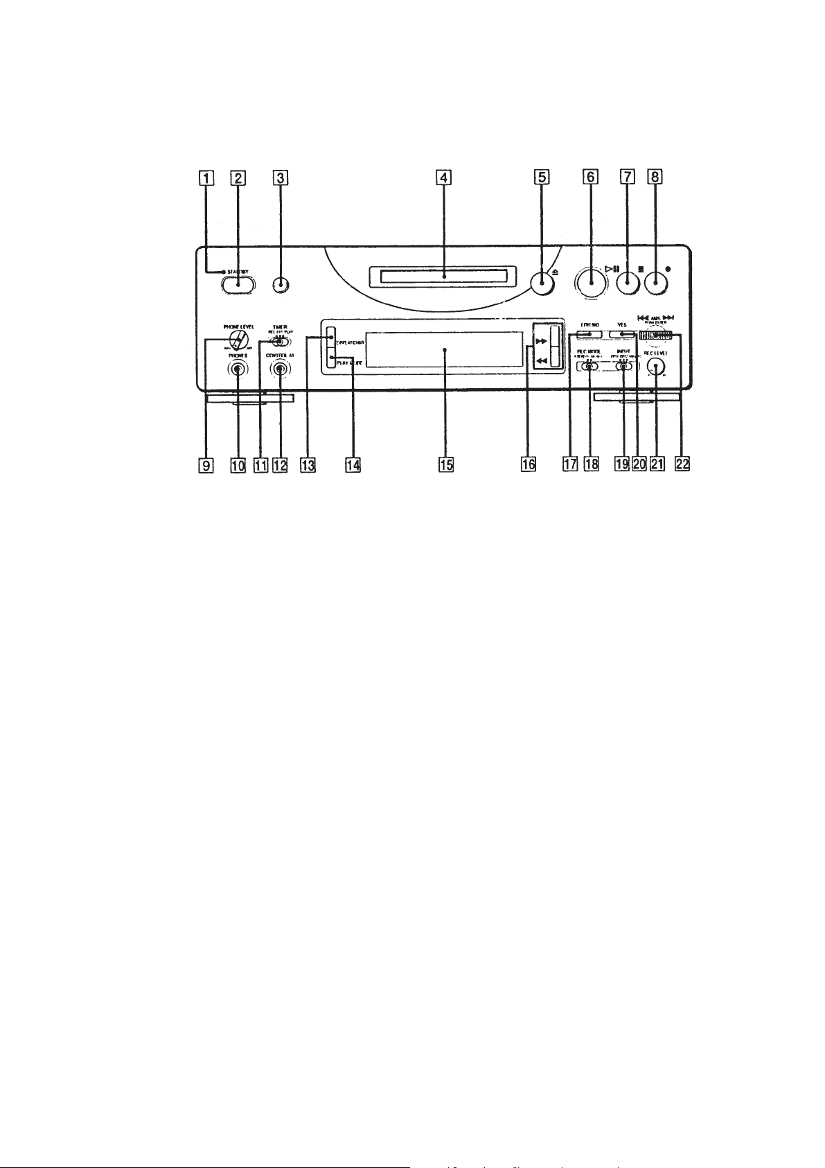
Front Panel
SECTION 2
GENERAL
Location of Parts and Controls
1 STANDBY lamp
2 1/u (Power) switch
3 Remote sensor
4 DISK compartment
5 § button
6 ·P button
7 p button
8 r button
9 PHONE LEVEL knob
10 PHONES jack
11 TIMER switch
12 CONTROL A1 jack
13 DISPLAY/CHAR button
14 PLAY MODE button
15 DISPLAY window
16 0/) button
17 EDIT/NO button
18 REC MODE switch
19 INPUT switch
20 YES button
21 REC LEVEL knob
22 AMS dial
• AMS is the abbreviation for Automatic Music Sensor.
– 9 –
Page 10
This section is extracted from
instruction manual.
– 10 –
Page 11
– 11 –
Page 12
– 12 –
Page 13
– 13 –
Page 14
– 14 –
Page 15
– 15 –
Page 16
– 16 –
Page 17
– 17 –
Page 18
– 18 –
Page 19
– 19 –
Page 20
– 20 –
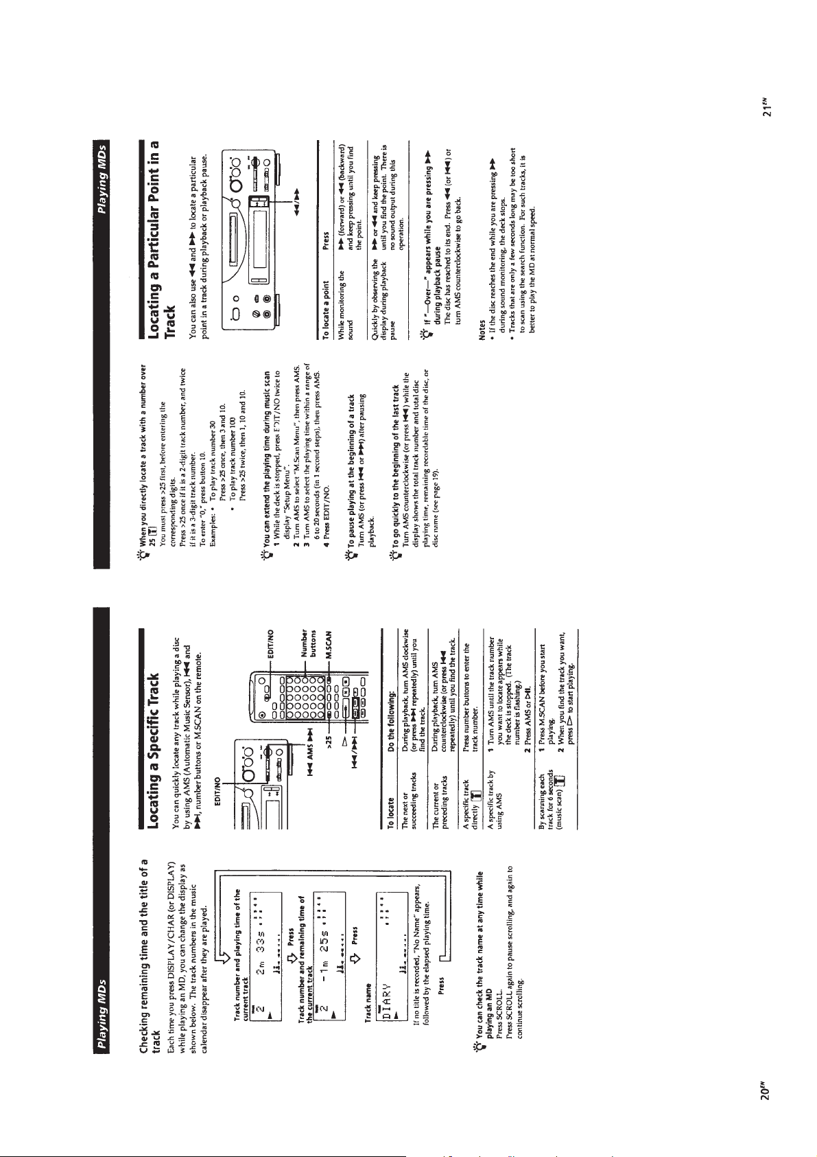
Page 21
– 21 –
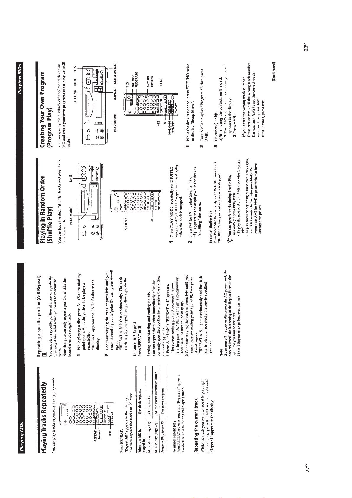
Page 22
– 22 –
Page 23
– 23 –
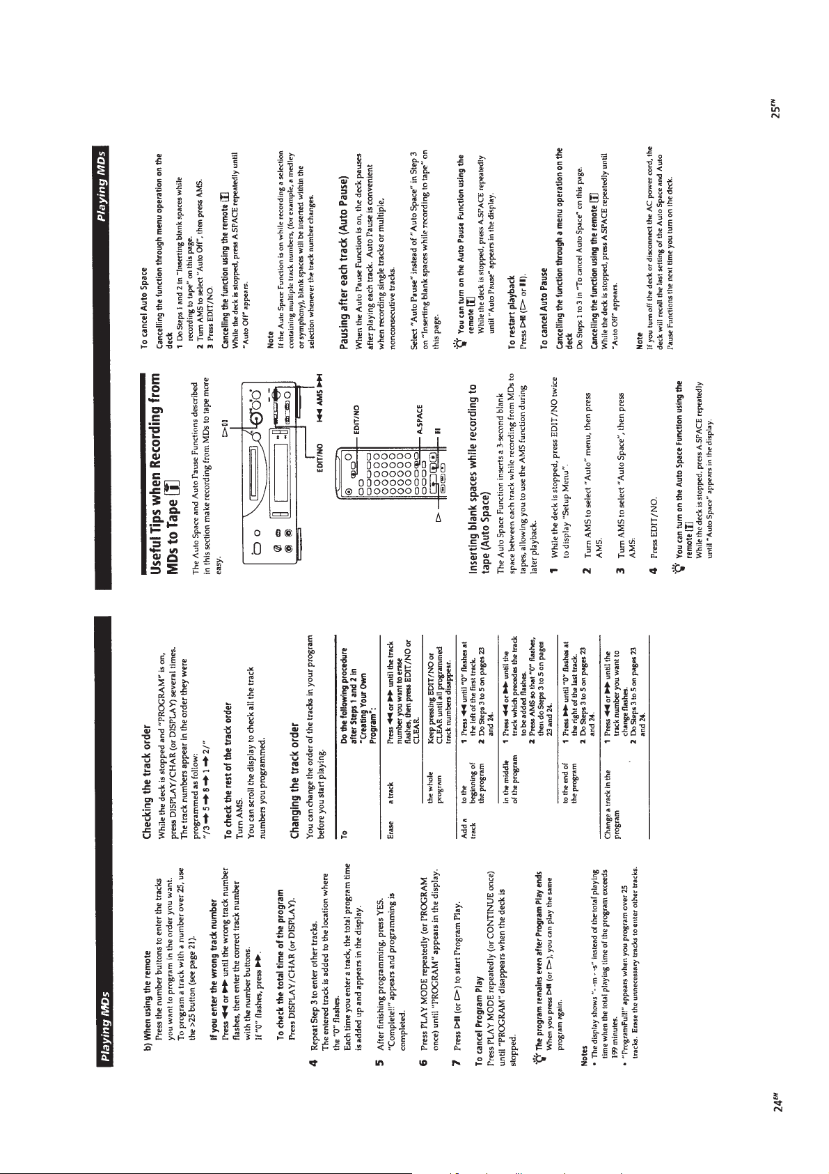
Page 24
– 24 –
Page 25
– 25 –
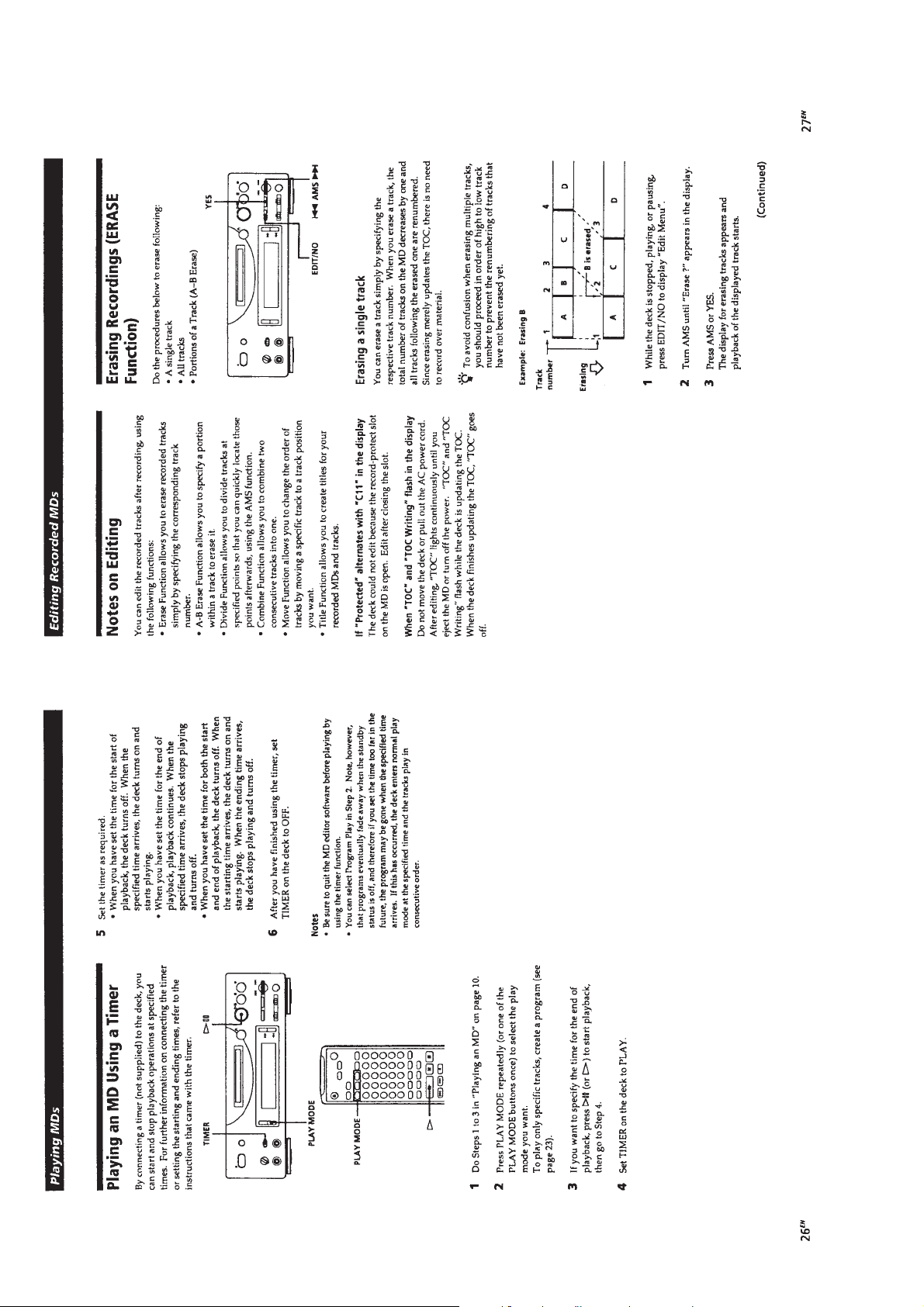
Page 26

– 26 –
Page 27

– 27 –
Page 28

– 28 –
Page 29

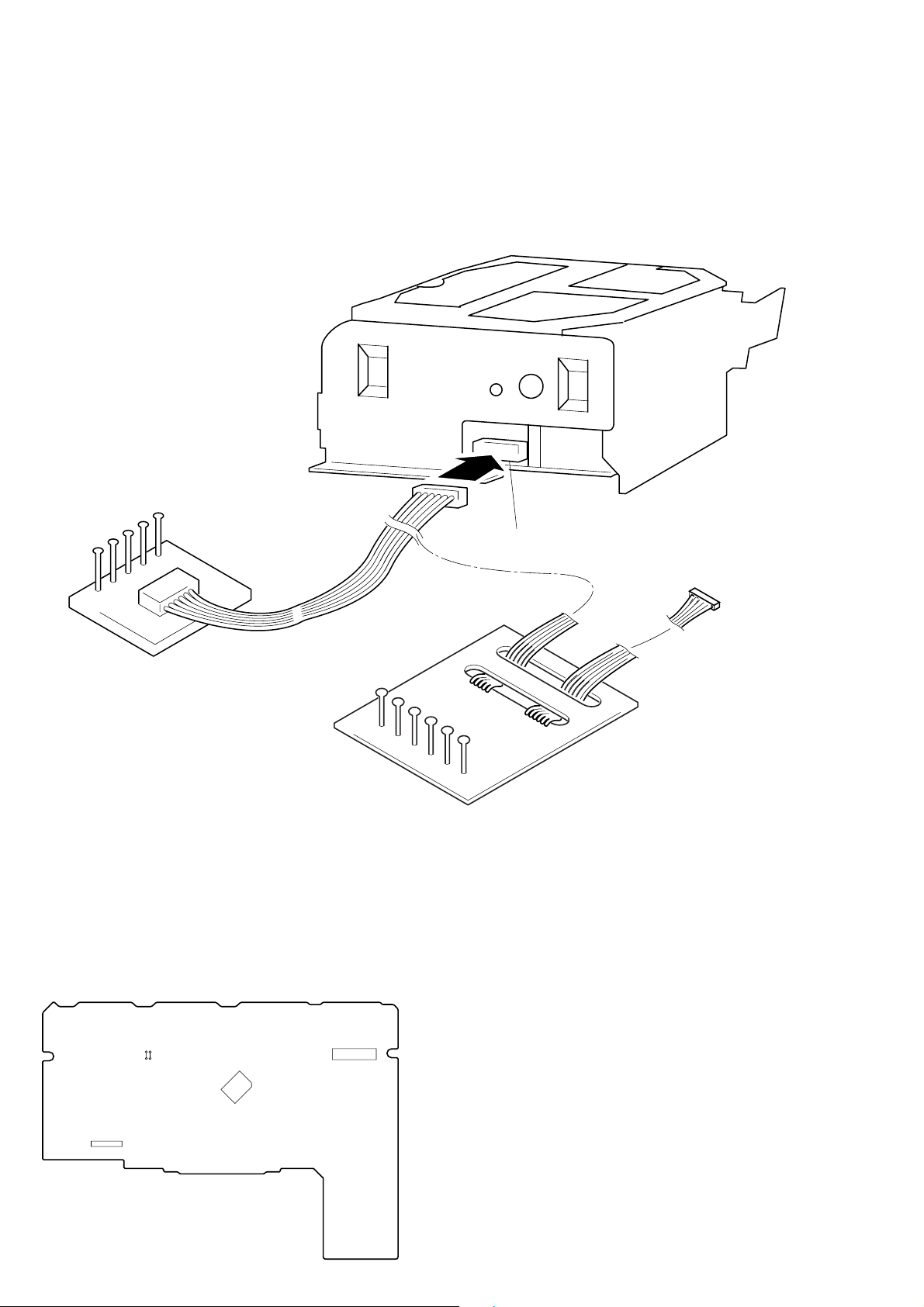
SECTION 3
DISASSEMBLY
Note: Follow the disassembly procedure in the numerical order given.
3-1. FRONT PANEL
7
Front panel assembly
3
Connector (CN403)
2
Connector
(CN800)
6
Three claws
5
Four screws (BVTP3x10)
4
Lead (With connector)
1
Flat type wire
(23core)
– 29 –
Page 30

3-2. BACK PANEL AND MAIN BOARD
!£
Back panel
!¢
Main board
8
Two screws (BVTP3x10)
2
Connector (CN301)
3
Two screws
(PTTWH3x6)
1
Connector (CN306)
4
Two screws
(PTTWH3x6)
7
Flat type wire
(29core)
5
Power
trnasformer
6
Flat type wire
(19core)
!™
Four screws (BVTP3x10)
!º
Three screws (BVTP3x10)
9
Screw
(BVTP3x10)
Note for installation
Install the Back panel as shown
in the figure.
Back panel
!¡
PC board holder
Chassis
– 30 –
Page 31

3-3. BRACKET (T)/(L)/(R)
2
Bracket (T)
6
Two screws
(BVTT2x3)
7
Bracket (L)
1
Four screws
(BVTT2x3)
4
Screw
(BVTT2x3)
5
Bracket
(joint)
3
Screw
(BVTT2x3)
3-4. SUB CHASSIS
1
Two step screws
5
Sub chassis
3
Two insulators
Part A
2
Two step screws
4
Two insulators
8
Two screws
(BVTT2x3)
Part A
Part A
9
Bracket (R)
NG
OK
– 31 –
Take care so that the part A
may be right position when installing.
Page 32

3-5. SHUTTER ASSEMBLY
2
Shaft (shutter)
1
Stopper washer
3
Shutter assembly
Shutter assembly
Shaft (lid)
Shaft (shutter)
Hole A
When installing, install the shaft (shutter) into the hole A
as shown in the figure before installing the shaft (lid) into
the hole B.
Hole B
– 32 –
Page 33

3-6. SLIDER COMPLETE ASSEMBLY
1
Screw
(M1.7x2)
2
Retainer (gear)
3
Set the shaft of Gear (LA) to be at the
position in the figure.
4
Remove the slider complete assembly
in the direction of arrow with putting
out of two claws.
Install the part A of lever (head up)
to pass over the slider complete assembly.
Take care not to damage the
detective switch.
Part A
OK
NG
Slider complete assembly
45˚
claw
claw
• Note for installation of Slider complete assembly
– 33 –
Page 34

SECTION 4
TEST MODE
4-1. PRECAUTIONS FOR USE OF TEST MODE
(1)As loading related operations will be performed regardless of the test mode operations being performed, be sure to check that the disc is
stopped before setting and removing it.
Even if § button is pressed while the disc is rotating during continuous playback, continuous recording, etc., the disc will not stop
rotating.
Therefore, it will be ejected while rotating.
Be sure to press the EDIT/NO button to stop the disc rotation before pressing the § button.
(2)Detection of the rec-proof tab is not performed in the test mode. Therefore, the contents of the recorded contents will be erased when
operations in the mode for emitting the recording laser are performed (4-1-1) or when the r button is pressed. Consequently, be careful
not to set the continuous recording mode and traverse adjustment mode with a disc whose contents cannot be erased in the test mode.
4-1-1. Recording Laser Emission Mode and Operating Buttons
*Continuous recording mode (CREC MODE)
*Traverse adjustment mode (EFBAL ADJUST)
*Laser power adjustment mode (LDPWR ADJUST)
*Laser power check mode (LDPWR CHECK)
*Traverse (MO) check (EF MO CHECK)
*Traverse (MO) adjustment (EF MO ADJUST)
*When pressing the r button.
4-2. SETTING THE TEST MODE
While pressing the AMS dial, connect the power plug to the outlet and release the AMS dial.
4-3. EXITING THE TEST MODE
With the TIMER knob set to “OFF”, press the POWER button. The STANDBY state will be set.
4-4. BASIC OPERATIONS OF THE TEST MODE
All operations are performed using the AMS dial, YES button, and EDIT/NO button.
The functions of these buttons are as follows.
Function name
AMS knob
YES button
EDIT/NO button
Changes parameters and modes
Proceeds onto the next step. Finalizes input.
Returns to previous step. Stops operations.
Function
– 34 –
Page 35

4-5. SELECTING THE TEST MODE
There are altogether 23 test modes, shown in the following table. Rotating the AMS dial to the right switches to the mode below the current
mode in the table while rotating to the left switches to the mode above. Each time the EDIT/NO button is pressed, the display changes in the
following order;
“TEMP CHECK” n “TEMP ADJUST” n “SLED MO VE” n “TEMP CHECK”...
Display
TEMP CHECK
LDPWR CHECK
EF MO CHECK
EF CD CHECK
FBIAS CHECK
CPLAY MODE
CREC MODE
Scurve CHECK
DETRK CHECK
TEMP ADJUST
LDPWR ADJUST
EF MO ADJUST
EF CD ADJUST
FBIAS ADJUST
EEP MODE
MANUAL CMD
SVDATA READ
ERR DP MODE
SLED MOVE
ACCESS MODE
0920 CHECK
HEAD ADJUST
V er@@@@@
Contents
Temperature compensation offset check
Laser power check
Traverse (MO) check
Traverse (CD) check
Focus bias check
Continuous playback mode
Continuous recording mode
S curve check
Detrack check
Temperature compensation offset adjustment
Laser power check
Traverse (MO) check
Traverse (CD) check
Focus bias check
Nonvolatile memory control
Command transfer
Status display
Error history display, clear
Sled check
Access check
Outermost circumference check
Head position check
Microprocessor version display
Mark
(X)
(X)
(X) (!)
(X)
(X)
(X)
(X)
(X)
(X)
• For details of each adjustment mode , refer to the items in “5. Electric Adjustments”. For details of “ERR DP MODE”, refer to the selfdiagnosis function on page 2.
• If other modes are set accidentally, press the EDIT/NO button to exit that mode.
• As items marked (X) in the “Mark” column are not used during servicing, they are not described here. If these modes ar e set accidentally,
press the EDIT/NO button to exit that mode. Be especially careful with items marked (!) as they will overwrite the non-volatile memory,
and as a result, the unit will not operate normally.
4-5-1. Operating the Continuous Playback Mode
1. Entering the continuous playback mode
(1) Set the disc in the unit. (Recordable discs or discs for playback only).
(2) Rotate the AMS dial and display “CPLAY MODE”.
(3) Press the YES button to change the display to “CPLAY MID”.
(4) When access completes, the display changes to “C1=
Note: The numbers “
” displayed indicate the error rate and “ADER”.
AD= ”.
2. Changing the part to be played back
(1) When th YES button is pressed during continuous playback, the display changes as below, and the played back part can be changed.
“CPLAY MID” n “CPLAY OUT” n “CPLAY IN”
(2) When access completes, the display changes to “C1=
Note: The numbers “
” displayed indicate the error rate and “ADER”.
AD= ”.
3. Ending the continuous playback mode
(1) Press the EDIT/NO button. The display changes to “CPLAY MODE”.
(2) Press the § button to remove the disc.
Note:The playback start addresses for IN, MID, and OUT are as follows. To display the playback position address on the display, press
the DISPLAY/CHAR button to display “CPLAY(
)”.
IN: 40h cluster
MID: 300h cluster
OUT:700h cluster
– 35 –
Page 36

4-5-2. Operating the Continuous Recording Mode
1. Entering the continuous recording mode
1 Set a recordable disc in the unit. (Refer to Note 3.)
2 Rotate the AMS dial and display “CREC MODE”.
3 Press the YES button to change the display to “CREC MID”.
4 When access completes, the display changes to “CREC ( )” and the REC display lights up.
Note: The numbers “
” displayed indicate the recording position address.
2. Changing the part to be recorded
1 When th YES button is pressed during continuous recording, the display changes as below and the recorded part can be changed.
The REC display is off while changing.
“CPLAY MID” n “CPLAY OUT” n “CPLAY IN”
2 When access completes, the display changes to “CREC MODE”, and the REC display lights up.
Note: The numbers “
” displayed indicate the recording position address.
3. Ending the continuous recording mode
1 Press the EDIT/NO button. The display changes to “CREC (
)”, and the REC display lights up.
2 Press the § button to remove the disc.
Note 1: The recording start addresses for IN, MID, and OUT are as follows.
IN: 40h cluster
MID: 300h cluster
OUT: 700h cluster
Note 2: The EDIT/NO button can be used to stop recording anytime.
Note 3: The rec-proof tab will not be detected during the test mode. Be careful not to set the continuous recording mode with a disc whose
contents cannot be erased.
Note 4: Do not perform continuous recording for long periods of time above 5 minutes.
Note 5: During continuous recording, be careful not to apply vibration.
4-5-3. Non-Volatile Memory Mode (EEP MODE)
This mode reads and writes the contents of the non-volatile memory.
It is not used in servicing. If set accidentally, press the EDIT/NO button immediately to exit it.
4-6. FUNCTIONS OF OTHER BUTTONS
Function
·P
p
)
0
r REC
POWER (*NOTE)
(TIMER : PLAY or REC)
PLAY MODE
DISPLAY/CHAR
§
POWER (*NOTE)
(TIMER: OFF)
Sets continuous playback when pressed in the STOP state. T urns ON/OFF the tracking servo when pressed during continuous
playback.
Stops the continuous playback and recording.
Moves the sled to the external circumference only while the button is pressed.
Moves the sled to the internal circumference only while the button is pressed.
Turns ON/OFF recording during continuous playback.
Switches between bit and groove when pressed.
Switches the spindle servo mode (CLVS ˜ CLV A).
Switches the displayed contents when pressed.
Ejects the disc.
Exits the test mode.
*Note: The function of the POWER button changes according to the position of the TIMER knob.
Contents
– 36 –
Page 37

4-7. DISPLAYS DURING TEST MODE
Mode display
Error rate display
Address display
Auto gain display (Not used in servicing)
Detrack check display (Not used in servicing)
IVR display (Not used in servicing)
The display changes according to the following sequence each time the DISPLAY/CHAR button is pressed.
1. Mode display
“TEMP ADJUST” and “CPLAYMODE” are displayed.
2. Error rate display
The error rate is displayed as follows.
C1=ππππ AD=ππ
C1=:Indicates the C1 error.
AD=:Indicates ADER.
3. Address display
The address is displayed as follows.
(MO:Recordable discs, CD:Discs for playback only)
At this time, pressing the 1/u button with the TIMER knob set to
PLAY switches the display between groove and bit.
h=ππππs=ππππ(MO bit and CD)
h=ππππa=ππππ (MO groove)
h=Indicates the header address.
s=Indicates the SUBQ address.
a=Indicates the ADIP address.
Note:Displayed as “–” when servo is operated.
4. Auto gain display (Not used in servicing)
The auto gain is displayed as follows.
AG=ππ/ππ.ππ
5. Detrack check display (Not used in servicing)
The detrack is displayed as follows.
ADR=πππππππ
6. IVR display (Not used in servicing)
IVR is displayed as follows.
[ππ][ππ][ππ
Meanings of other displays
Display
¢
P
REC
–SYNC
A.SPACE
OVER
REPEAT
A-B
TRACK
DISC
DATE
CLOCK
Currently continuous playback (CLV:ON)
Tracking servo OFF
Recording mode ON
CLV low speed mode
ABCD adjustment completed
Tracking offset cancel ON
Tracking auto gain OK
Focus auto gain OK
Bit
High reflection rate
CLV-S
CLV LOCK
When Lit
Contents
When Off
STOP (CLV:OFF)
Tracking servo ON
Recording mode OFF
CLV normal mode
Tracking offset cancel OFF
Groove
Low reflection
CLV-A
CLV UNLOCK
– 37 –
Page 38

SECTION 5
d
ELECTRICAL ADJUSTMENTS
5-1. PRECAUTIONS FOR CHECKING LASER DIODE
EMISSION
When checking the emission of the laser diode during adjustments,
never view directly from the top as this may cause blindness.
5-2. PRECAUTIONS FOR USE OF OPTICAL PICK-
UP (KMS-260A)
As the laser diode in the optical pick-up is easily damaged by static
electricity, solder the laser tap of the flexible board when using it.
Before disconnecting the connector, solder first. Before connecting
the connector, be careful not to remove the solder . Also take adequate
measures to prevent damage by static electricity . Handle the flexible
board with care as it breaks easily.
Pick-up
Laser tap
Flexible boar
5-3. PRECAUTIONS FOR ADJUSTMENTS
1) When replacing the following parts, perform adjustments and
checks marked ¬ in the order shown in the following table.
Optical
Pick-up
1. Temperature
compensation
offset
adjustment
2. Laser power
adjustment
3. Traverse
adjustment
4. Focus bias
adjustment
5. Error rate check
IC171
¬¬G¬
¬G¬¬
¬G¬¬
¬G¬¬
¬G¬¬
2) Perform the adjustment in the test mode.
After completing the adjustments, exit the test mode.
3) Perform the adjustments in the order shown.
4) Use the following tools and measuring devices.
• Check disc (MD) TDYS-1
(Parts No.:4-963-646-01)
• Laser power meter LPM-8001
(Parts No.:J-2501-046-A)
• Oscilloscope (Measure after calibration of the probe).
• Digital voltmeter
• Thermometer
• Jig for checking the BD board waveform
(Parts No.:J-2501-124-A)
5) When observing several signals on the oscilloscope, etc., make
sure that the VC and ground do not connect inside the
oscilloscope.
(The VC and ground will short-circuit.)
6) Using the above jig enables the waveform to be checked without
the need for soldering.
(Refer to Servicing Note on page 5.)
BD Board
IC101, IC121, IC192
D101
5-4. CREATING THE CONTINUOUSLY RECORDED
DISC
• The disc is used for the focus bias adjustment and error rate check.
The following describes how to create a continuously recorded
disc.
1. Insert a disc (blank disc) commercially available.
2. Rotate the AMS knob to display “CREC MODE”.
3. Press the YES button to display “CREC MID”.
“CREC (0300)” will be momentarily displayed and recording
started.
4. Complete recording within 5 minutes.
5. Press the NO button and stop recording.
6. Press the § button and remove the disc.
Create the continuous recorded disc for adjusting the focus bias
and checking the error rate as described above.
Note:
• Be careful not to apply vibrations during continuous recording.
– 38 –
Page 39

5-5. TEMPERATURE COMPENSATION OFFSET
ADJUSTMENT
Save the current temperature data in the non-volatile memory as
the 25 °C standard data.
Note:
1. Normally, this adjustment should not be performed.
2. Set the surrounding temperature to 22 to 28 °C when performing
this adjustment.
Also perform this adjustment immediately after the power is
turned on when the internal temperature of the unit is the same
as the surrounding temperature (22 to 28 °C).
3. After replacing D101, perform this adjustment after the
temperature of parts reach the surrounding temperature.
Adjusting Procedure:
1. Rotate the AMS knob, to display “TEMP ADJUST”.
2. Press the YES button and select the “TEMP ADJUST” mode.
3. “TEMP= ” and the current temperature data are displayed.
4. To save the data:Press the YES button.
If not saving the data:Press the NO button.
5. When the YES button is pressed, “TEMP= SAVE” is
displayed, and then “TEMP ADJUST” is displayed again.
“TEMP ADJUST” is displayed again immedia tely after the NO
button is pressed.
Specification:
TEMP= should be E0 to EF. F0 to FF, 00 to 0F, 10 to 1F and 20
to 2F.
5-6. LASER POWER ADJUSTMENT
Connection:
Laser power
meter
2. Rotate the AMS knob to display “LDPWR ADJUST”.
(Laser power:For adjustment)
3. Press the YES button once to display “LD 0.9mW $@@”.
4. Rotate the AMS knob so that the laser power meter reads 0.86
to 0.92 mW. Set the range knob of the laser power meter to 10
mW, press the YES button, and save the adjustment results in
the non-volatile memory. (“LD SAVE $ ” is displayed
momentarily.)
5. “LD 7.0 mW $ ” is next displayed.
6. Rotate the AMS knob so that the laser po wer meter reads 6.9 to
7.1 mW, press the YES button, and sa ve the adjustment results
in the non-volatile memory. (“LD SAVE $ ” is displayed
momentarily.)
Note:Do not emit 7.0 mW continuously for more than 15
seconds.
7. Rotate the AMS knob to display “LDPWR CHECK”.
8. Press the YES button once to display “LD 0.9mW $ ”.
Check that the laser power meter reading is 0.85 to 0.91 mW.
9. Press the YES button another time to display “LD 7.0mW $
”.
Check that the readings of the laser power meter and digital
voltmeter become the specified v alue.
Specified value
Laser power meter reading:7.0 ± 0.1 mW
Digital voltmeter reading:Value displayed on optical pick-up label
± 10%
(Optical pick-up label)
KMS
260A
27X40
B0825
N
Iop = 82.5 mA in this case
Iop (mA) = Digital voltmeter reading (mV)/1 (Ω)
Optical pick-up
objective lens
Digital
Voltmeter
BD board
CN110 Pin
CN110 Pin
5
4
(I+3V)
(IOP)
Adjusting Procedure:
1. Set the laser power meter on the objective lens of the optical
pick-up from the disc slot. (If it cannot be set properly, pr ess the
0 or ) button to move the optical pick-up).
Connect the digital voltmeter to Pin 5 (I+3V) and Pin 4 (IOP)
of CN110.
10.Press the NO button to display “LDPWR CHECK” and stop
the laser emission.
(The NO button is effective at all times to stop the laser
emission.)
– 39 –
Page 40

5-5. TEMPERATURE COMPENSATION OFFSET
ADJUSTMENT
Save the current temperature data in the non-volatile memory as
the 25 °C standard data.
Note:
1. Normally, this adjustment should not be performed.
2. Set the surrounding temperature to 22 to 28 °C when performing
this adjustment.
Also perform this adjustment immediately after the power is
turned on when the internal temperature of the unit is the same
as the surrounding temperature (22 to 28 °C).
3. After replacing D101, perform this adjustment after the
temperature of parts reach the surrounding temperature.
Adjusting Procedure:
1. Rotate the AMS knob, to display “TEMP ADJUST”.
2. Press the YES button and select the “TEMP ADJUST” mode.
3. “TEMP= ” and the current temperature data are displayed.
4. To save the data:Press the YES button.
If not saving the data:Press the NO button.
5. When the YES button is pressed, “TEMP= SAVE” is
displayed, and then “TEMP ADJUST” is displayed again.
“TEMP ADJUST” is displayed again immedia tely after the NO
button is pressed.
Specification:
TEMP= should be E0 to EF. F0 to FF, 00 to 0F, 10 to 1F and 20
to 2F.
5-6. LASER POWER ADJUSTMENT
Connection:
Laser power
meter
2. Rotate the AMS knob to display “LDPWR ADJUST”.
(Laser power:For adjustment)
3. Press the YES button once to display “LD 0.9mW $@@”.
4. Rotate the AMS knob so that the laser power meter reads 0.86
to 0.92 mW. Set the range knob of the laser power meter to 10
mW, press the YES button, and save the adjustment results in
the non-volatile memory. (“LD SAVE $ ” is displayed
momentarily.)
5. “LD 7.0 mW $ ” is next displayed.
6. Rotate the AMS knob so that the laser po wer meter reads 6.9 to
7.1 mW, press the YES button, and sa ve the adjustment results
in the non-volatile memory. (“LD SAVE $ ” is displayed
momentarily.)
Note:Do not emit 7.0 mW continuously for more than 15
seconds.
7. Rotate the AMS knob to display “LDPWR CHECK”.
8. Press the YES button once to display “LD 0.9mW $ ”.
Check that the laser power meter reading is 0.85 to 0.91 mW.
9. Press the YES button another time to display “LD 7.0mW $
”.
Check that the readings of the laser power meter and digital
voltmeter become the specified v alue.
Specified value
Laser power meter reading:7.0 ± 0.1 mW
Digital voltmeter reading:Value displayed on optical pick-up label
± 10%
(Optical pick-up label)
KMS
260A
27X40
B0825
N
Iop = 82.5 mA in this case
Iop (mA) = Digital voltmeter reading (mV)/1 (Ω)
Optical pick-up
objective lens
Digital
Voltmeter
BD board
CN110 Pin
CN110 Pin
5
4
(I+3V)
(IOP)
Adjusting Procedure:
1. Set the laser power meter on the objective lens of the optical
pick-up from the disc slot. (If it cannot be set properly, pr ess the
0 or ) button to move the optical pick-up).
Connect the digital voltmeter to Pin 5 (I+3V) and Pin 4 (IOP)
of CN110.
10.Press the NO button to display “LDPWR CHECK” and stop
the laser emission.
(The NO button is effective at all times to stop the laser
emission.)
– 39 –
Page 41

5-8. FOCUS BIAS ADJUSTMENT
Adjusting method:
1. Load a continuously recorded disc (Refer to “5-4. Creating the
Continuously Recorded Disc”.)
2. Rotate the AMS knob to display “CPLAY MODE”.
3. Press the YES button to display “CPLAY MID”.
4. When “C1= AD= ” is displayed, press the NO button.
5. Rotate the AMS knob to display “FBIAS ADJUST”.
6. Press the YES button to display “ / a= ”.
The first four digits indicate the C1 error rate, the two digits
after the “/” indicate ADER and the two digits after “a=” indicate
the focus bias value.
7. Rotate the AMS knob in the clockwise direction, and look for
the focus bias value at which the C1 error rate becomes
approximately 220 (Refer to Note 2).
8. Press the YES button to display “ / b= ”.
9. Rotate the AMS knob in the counterclockwise direction, and
look for the focus bias value at which the C1 error rate becomes
220.
10. Press the YES button to display “ / b= ”.
11. Chec k that the C1 error rate is below 50 and that ADER is 00,
and press the YES button.
12. If the value of “( )” in the “ - - ( )” displayed is
above 20, press the YES button.
If below, press the NO button and start from step 2 again.
13. Press the § button and remove the continuously recorded disc.
Note 1: The following figure shows the relation between the C1
error and focus bias value. Look for points a and b in the
following figure by the adjustment above. The focus
position (point c) is automatically calculated from points a
and b.
Note 2: As the C1 error rate changes, use the average value in the
adjustment.
C1 error
220
Focus bias value
(F. BIAS)
bc a
5-9. ERROR RATE CHECK
5-9-1. CD ERROR RATE CHECK
Checking Procedure:
1. Load a check disc (MD) TDYS-1.
2. Rotate the AMS knob to display “CPLAY MODE”.
3. Press the YES button to display “CPLAY MID”.
4. “C1= AD= ” is displayed.
5. Check that the C1 error rate is below 20.
6. Press the NO button to stop playback. Then press the § button
and remove the check disc (MD).
5-9-2. MO Error Rate Checking
Checking Procedure:
1. Load a continuously recorded disc (Refer to “5-4. Creating the
Continuously Recorded Disc”.)
2. Rotate the AMS knob to display “CPLAY MODE”.
3. Press the YES button to display “CPLAY MID”.
4. “C1= AD= ” is displayed.
5. Check that the C1 error rate is below 50 and ADER is 00.
6. Press the NO button to stop playback. Then press the § button
and remove the disc.
5-10. FOCUS BIAS CHECK
Change the focus bias value and check the focus tolerance amount.
Checking Procedure:
1. Load a continuously recorded disc (Refer to “5-4. Creating the
Continuously Recorded Disc”.)
2. Rotate the AMS knob to display “CPLAY MODE”.
3. Press the YES button to display “CPLAY MID”.
4. When “C1= AD= ” is displayed, press the NO button.
5. Rotate the AMS knob to display “FBIAS CHECK”,
6. Press the YES button to display “
The first four digits indicate the C1 error , the two digits after the
“/” indicate ADER and the two digits after “c=” indicate the
focus bias value.
Check that the C1 error is below 50 and ADER is 00.
7. Press the YES button to change the display to “ / b=
”.
Check that the C1 error does not drop below 220 and ADER
does not remain above 00.
8. Press the YES button to change the display to “ / a=
”.
Check that the C1 error does not drop below 220 and ADER
does not remain above 00.
9. Press the NO button, press the § button next, and remov e the
continuously recorded disc.
/ c= ”.
Note 1:If the C1 error is above 220 or ADER is above 00 only for
point a (step 8 above) and point b (step 7 above), the focus
bias may not be adjusted properly. In this case, adjust again.
– 41 –
Page 42

5-11. ADJUSTING POINTS AND CONNECTING POINTS
[BD BOARD] (SIDE A)
CN110
RF I+3V
VC
CN101
D101
[BD BOARD] (SIDE B)
NOTE
IOP
TEO
IC192
IC171
IC101
IC121
NOTE:It is useful to use the jig. for checking the waveform. (Refer
to Servicing Note on page 6.)
– 42 –
Page 43

6-1. CIRCUIT BOARDS LOCATION
d
TRANS board
SW board
SECTION 6
DIAGRAMS
BACK UP board
VOLTAGE SELECTOR board
MAIN boar
PANEL board
BD board
ROTARY ENCODER (S701)
VOLUME board
– 43 –
Page 44

MDS-PC1
6-2. BLOCK DIAGRAMS
– BD SECTION –
• SIGNAL PATH
: PB
: REC
:PB(Digital out)
:REC(Digital in)
OPTICAL PICK-UP BLOCK
(KMS-260A/J1N)
DETECTOR
F
IJ
C
B
D
A
E
VC
PD
LD
ILCC
HR901
OVER WRITE
HEAD
VC
D101
LASER ON
SW
Q101
15
14
10
APC
Q162,163
HEAD
DRIVE
Q181,182
I
1
J
2
A
4
B
5
C
6
D
7
E
8
F
9
VC
3
TEMPR
TEMPI
PD
48 47 46 40
RFO
MORFI
MORFO
RF AMP
IV AMP
IV AMP
CVB
TEMP
AMP
APC
11
11
14
15
17
AGCI
BALANCE
APCREF
12
VCC
E-F
4
IC122
RF AMP
IC101
RF AGC & EQ
BPF
EQADJ
1
2
OVER WRITE HEAD DRIVE
IC181
3
18 2
9
P-P
PEAK
&
BOTTOM
ABCD
AMP
FOCUS
ERROR
AMP
AT
AMP
TRACKING
ERROR
AMP
SERIAL
VICONV
3TADJ
2522 23
WBLADJ
PARALLEL
DECODER
1
18
RF
38
AUX
33 66
BOTM
36
PEAK
37
ABCD
35
FE
34 65
BPF
ADFM
ADIN
ADFG
CSLED
SWDT
SCLK
XLAT
FOCNT
VC
31
29
30
32
TE
26
SE
28
27
16
17
18
20
VC
VC
Q180
FILTER
VC
DIGITAL SERVO SIGNAL PROCESSOR, DIGITAL SIGNAL PROCESSOR
EFM/ACIRC ENCODER/DECODER, SHOCK-PROOF MEMORY CONTROLLER,
EFMO
100
PCO
58
FILI
59
FILO
60
CLTV
61
RFI
55
AUX1
BOTM
63
PEAK
62
ABCD
64
EE
VC
67
TE
74
SE
73
ADFG
78
DTRF
82
CKRF
81
XLRF
80
FOCNT
79
ATRAC ENCODER/DECODER, 2M-BIT DRAM
PLL
ANALOG
MUX
ADIP
DEMODULATOR/
DECODER
SPINDLE
SERVO
SPRD
93
ACIRC,
ENCODER/
DECODER
SPFD
94
EFM,
FG IN
95 10
IC121
XRST
RECP
13
15 14
TX
SHOCK
RESISTANT
MEMORY
CONTROLLER
APC
APCREF
FFDR
XINIT
A/D
CONVERTER
PWM
GENERATOR
FRDR
TFDR
TRDR
ATRAC
ENCODER/
DECODER
SAMPLING
RATE
CONVERTER
SERVO
DSP
3
20
SFDR
SRDR
D0 D3 A0 A9
91928586898883
47 • 46 • 48 • 49
DIGITAL
AUDIO
I/F
CLOCK
GENERATOR
SUBCODE
PROCESSOR
MONITOR
CONTROL
CPU
I/F
AUTO
SEQUENCER
32 29 • 34 38 • 43
DIN
ADDT
DADT
DOUT
XBCK
LRCK
OSCI
SQSY
DQSY
MNT3
MNT2
MNT1
MNT0
SENS
SRDT
SCLK
SWDT
XLAT
XWE
XRAS
XCAS
XOE
21
23
24
22
26
25
16
11
12
4
3
2
1
9
8
6
5
7
45
44
42
41
1 5
BUFFER
IC123
DRAM
IC124
3
XWE
4
XRAS
17
XCAS
16
XOE
1
DQ1
•
2
•
18
•
DQ4
19
A0
6
9
•
11
15
•
A9
5
SCTX
XINT
DIN
ADDT
DADT
DOUT
BCK
LRCK
512FS
SQSY
DQSY
MNT3
MNT2
MNT1
MNT0
SENS
SRDT
SCLK
SWDT
XLAT
LDON
MAIN
SECTION
HF
MODULE
TRAKING
COIL
FOCUS
COIL
M902
SLED MOTOR
M901
SPINDLE MOTOR
09
TRK–
TRK+
FSC+
FSC–
SLED+
M
SLED–
SPDL+
M
SPDL–
HF MODULE
SW
IC103,Q102-104
SLED/SPINDLE MOTOR DRIVE
FOCUS/TRACKING COIL DRIVE
IC152
10
DRIVER
12
21
DRIVER
23
27
DRIVER
25
6
DRIVER
8
PSB
5
EEP ROM
IC171
TFDR
85
TRDR
86
FRDR
89
FFDR
88
SFDR
92
SRDR
91
SPFD
94
SPRD
93
XRST
16
M903
LOADING MOTOR
SDA
DETECT SW
S681 - 683,
S685 - 688
M
6
WRPWR
MOD
SDA
SCLSCL
LIMIT
REFLECT
PROTECT
CHACK IN
PACK OUT
PB P
REC P
LOAD-IN
LOAD-OUT
XRST
– 45 – – 46 –
Page 45

MDS-PC1
– MAIN SECTION –
DIN
DOUT
ADDT
DADT
SCTX
XINT
BCK
LRCK
512FS
SQSY
DQSY
MNT3
MNT2
MNT1
MNT0
SENS
SRDT
SCLK
SWDT
XLAT
BD
SECTION
09
LIMIT
REFLECT
PROTECT
CHACK IN
PACK-OUT
PB-P
REC-P
LDON
WRPWR
MOD
LOAD-IN
LOAD-OUT
SDA
SCL
XRST
BCK
LRCK
512FS
SCLK
SWDT
XLAT
2
10
DRIVE
LOADING MOTOR
DRIVE
IC311
1
DRIVE
DIGITAL
OUT
IC352
LOADING
Q311, 312
SLOCK
XBUSY
4
SW
DIGITAL
INPUT SELECTOR
IC315
8
2
5
18
76
68
66
77
65
32
33
31
71
74
70
72
51
53
60
59
69
75
73
5
54
6
55
56
78
79
67
1
13
80
20
XINT
SQSY
DQSY
MNT3 (SLOCK)
MNT2 (XBUSY)
MNT1 (SHOCK)
MNT0 (FOK)
SENS
SRDT
SCLK
SWDT
XLATCH
LIMIT-IN
REFLECT
PROTECT
CHACK IN
PACK-OUT
PB-P
REC-P
SYSTEM CONTROL
LDON
WR PWR
MOD
LDIN
LDOUT
LD LOW
SDA
SCL
DIG-RST
XOUT
13 15
X402
7MHz
2
4
86
SCTX
IC401
XIN
BUFFER
IC314 (1/2)
5
OPT SEL
AMUTE
CONTROL A1 OUT
CONTROL A1 IN
MONO/ST
KEY0
KEY1
KEY2
TIMER SW
SOURCE SW
JOG1
JOG0
REMOCOM
FLCLK
FLDATA
FLCS
P DOWN
CLOCKSET1
CLOCKSET0
STBY
A/D, D/A CONVERTER
MCK1
15
35 36
22
256CK
I/O
22MHz
XOUT
X201
IC201
XIN
5
BA501
LITHIUM
BATTERY
BACK +3.3V
+3V REG
IC192
SYS +3.3V
ANA +5V
CONVERTER
CONVERTER
PH +5V
RV702
INLM
55
INLP
A/D
D/A
1
INRP
INRM
+ L1
– L2
+ R1
– R2
1
5
4
6
56
1
2
41
39
30
32
SRESET
212
R-ch
R-ch
SWITCHING REG
+5V REG
+3.3V REG
+5V REG
BACK UP
IC501
BUFFER
IC314 (2/2)
24 23
17
16
1310
FRONT-END
IC101
LPF 1
15
MUTE
4
+6V
3
+B
–6V
–32V
14
+6V REG
IC541
–6V REG
–32V REG
+B
IC551
IC310
REC LEVEL
2526
R-ch
MUTE
SW
Q306
RECT
31
–B
23
13
D001,
D002
RECT
D007,
D008
RECT
D005,
006
RECT
D003,
004
FL701
RECT
D009
MUTE
Q102
AC
AC
2122
R-ch
R-ch
HEADPHONE
AMP
IC308
3 1
TR001
POWER
TRANSFORMAER
L
R
(ANALOG)
R
L
RV701
PHONE LEVEL
J401
S-LINK
CONTROL A1
CONTROL A1
AEP,UK
MAIN
POWER
S301
SP
VOLTAGE
SELECTOR
S301
IN
J101
LINE
OUT
R-ch
J702
J701
PHONES
AC
IN
• R-CH is omitted.
1
3
3
48ADA RES
12 3 RSTSYSTEM RST
49
87
7
100
97
95
94
91
88
21
22
83LED0 (POWER)
6
37
35
34
19
82
81
50
MATRIX
LED DRIVE
Q701
3 RM
DISPLAY DRIVER
SCK
62
SDATA
63
CS
61
RST
60
IC353
DIGITAL
IN
RESET
IC502
SW
IC701
+3.3V
(DIN)
SIRCS
RECEIVER
IC702
S1
S36
39
40
D1
54
D15
4
12
BCK
LRCK
512FS
27
18
16 DPD
SWDT
SCLK
XLAT
LEVEL SHIFT
Q203
D701
STANDBY
DADT
RES
CONTROL A1 DRIVER
FL701
FLUORESCENT
INDICATOR
TUBE
10 11
25 28 26
PH +5V
AC
I/O
CPU INTERFACE
19 20 21
Q485
+3V
(BD)
• SIGNAL PATH
: PB
: REC
:PB(Digital out)
:REC(Digital in)
• Abbreviation
SP :Singapore model.
– 47 – – 48 –
Page 46

THIS NOTE IS COMMON FOR PRINTED WIRING
0.46Vp-p
3.1Vp-p
22.581MHz
3.2Vp-p
44.1kHz
3.8Vp-p
11.29MHz
3.3Vp-p
44.1kHz
2.9Vp-p
22.578MHz
5Vp-p
22.58MHz
BOARDS AND SCHEMATIC DIAGRAMS.
(In addition to this, the necessary note is printed
in each block.)
WAVEFORMS
– BD SECTION – – MAIN SECTION –
1
1
– PANEL SECTION –
1
For schematic diagrams.
Note:
• All capacitors are in µF unless otherwise noted. pF: µµF
50 WV or less are not indicated except for electrolytics
and tantalums.
• All resistors are in Ω and
specified.
¢
•
• C : panel designation.
Note: The components identified by mark ! or dotted line
• U : B+ Line.
• V : B– Line.
• H : adjustment for repair.
• Voltages and waveforms are dc with respect to ground
• Voltages are taken with a VOM (Input impedance 10 MΩ).
• Waveforms are taken with a oscilloscope.
• Circled numbers refer to waveforms.
• Signal path.
• Abbreviation
: internal component.
with mark ! are critical for safety.
Replace only with part number specified.
under no-signal (detuned) conditions.
no mark : STOP
( ) : PLAY
< > : REC
Voltage variations may be noted due to normal production tolerances.
Voltage variations may be noted due to normal production tolerances.
E : PB
q : REC
a : PB (DIGITAL OUT)
r : REC (DIGITAL IN)
SP : Singapore model.
: Can not be measured.
∗
1
4
/
W or less unless otherwise
For printed wiring boards.
Note:
• X : parts extracted from the component side.
• Y : parts extracted from the conductor side.
•
p : parts mounted on the conductor side.
®
•
• b : Pattern from the side which enables seeing.
(The other layers' patterns are not indicated.)
: Through hole.
IC101 1, 2 I, J (PLAY mode)
2
IC101 4 A (PLAY mode)
3
IC101 8, 9 E, F (PLAY mode)
4
IC121 !§ OSCI
5
IC121 @∞ LRCK
6
2.822MHz
IC121 @§ XBCK
7
0.1Vp-p
0.06Vp-p
3.8Vp-p
7MHz
IC401 !£ XOUT
2
IC201 0 LRCK1, @• LRCK
3
2.822MHz
IC201 !¡ BCK1, @§ BCK
4
IC201 !∞ MCK1, @™ 256CK
22.553MHz
5
IC201 @∞ 512FS
6
IC201 #∞ XOUT
3.4Vp-p
3.6Vp-p
5.6Vp-p
3.7Vp-p
2.361MHz
IC701 %ª OSC1
Caution:
Pattern face side: Parts on the pattern f ace side seen from the
(Side B) pattern face are indicated.
Parts face side: Parts on the parts face side seen from the
(Side A) parts face are indicated.
• Indication of transistor
• Indication of transistor
C
These are omitted
EB
• Indication of transistor
ECB
These are omitted
IC121 @¶ FS256
8
3.2Vp-p
176.4kHz
IC121 (º FS4
– 49 – – 50 –
Page 47

MDS-PC1
6-3. SCHEMATIC DIAGRAM – BD (1/2) SECTION –
• See page 50 for Waveforms.
• See page 55 for Printed Wiring Board.
• See page 71 for IC Block Diagrams.
• See page 76 for IC Pin Functions.
– 51 –
(Page 54)(Page 53)
– 52 –
Page 48

6-4. SCHEMATIC DIAGRAM – BD (2/2) SECTION –
(Page 65) (Page 58) (Page 61)
(Page 51) (Page 52)
• See page 50 for Waveforms.
• See page 55 for Printed Wiring Board.
• See page 72 for IC Block Diagrams.
• See page 77 for IC Pin Functions.
MDS-PC1
– 53 –
– 54 –
Page 49

MDS-PC1
6-5. PRINTED WIRING BOARD – BD SECTION –
• See page 43 for Circuit Boards Location.
(Page 57)
• Semiconductor
Location
Ref. No. Location
D101 E-3
D181 C-9
D183 C-9
IC101 F-14
IC103 B-15
IC121 D-12
IC122 C-4
IC123 E-10
IC124 F-12
IC152 B-12
IC171 F-9
IC181 D-9
IC192 G-6
Q101 C-14
Q102 B-15
Q103 B-14
Q104 B-14
Q162 B-14
Q163 B-15
Q180 D-6
Q181 B-9
(Page 59) (Page 59)
Q182 B-9
– 55 –
– 56 –
Page 50

MDS-PC1
(Page 53)
6-6. PRINTED WIRING BOARD – SW SECTION –
• See page 43 for Circuit Boards Location.
(Page 55)
6-7. SCHEMATIC DIAGRAM – SW SECTION –
– 57 – – 58 –
Page 51

MDS-PC1
6-8. PRINTED WIRING BOARD – MAIN SECTION –
• See page 43 for Circuit Boards Location.
(Page 67)
(Page 67)
(Page 68)
(Page 56)
(Page 56)
: US
: AEP, UK, SP
• Semiconductor Location
Ref. No. Location
D001 E-10
D002 E-10
D003 E-10
D004 E-10
D005 D-11
D006 D-11
D007 D-9
D008 D-9
D009 E-9
D350 F-1
D485 A-8
D486 A-10
D501 C-10
D531 E-8
D541 C-3
D599 B-3
IC101 C-2
IC201 E-2
IC308 D-3
Ref. No. Location
IC310 E-8
IC311 G-1
IC314 B-5
IC315 B-6
IC352 A-4
IC353 A-3
IC401 D-5
IC501 C-9
IC502 A-10
IC541 C-3
IC551 B-3
Q102 D-3
Q202 D-3
Q203 E-3
Q306 D-10
Q311 G-1
Q312 G-1
Q485 A-9
– 59 – – 60 –
Page 52

6-9. SCHEMATIC DIAGRAM – MAIN (1/3) SECTION –
• See page 50 for Waveforms.
• See page 82 for IC Pin Functions.
MDS-PC1
(Page 53)
(Page 69)
– 61 –
(Page 65)
(Page 63)
(Page 65)
– 62 –
Page 53

MDS-PC1
6-10. SCHEMATIC DIAGRAM – MAIN (2/3) SECTION –
• See page 50 for Waveforms.
• See page 59 for Printed Wiring Board.
• See page 73 for IC Block Diagrams.
• See page 80 for IC Pin Functions.
(Page 69)
(Page 62)
L805 0µH
US
AEP, UK, SP
1µH
(Page 65)
– 63 – – 64 –
(Page 66)
Page 54

6-11. SCHEMATIC DIAGRAM – MAIN (3/3) SECTION –
• See page 50 for Waveforms.
• See page 59 for Printed Wiring Board.
• See page 75 for IC Block Diagrams.
MDS-PC1
(Page 63) (Page 64)
(Page 61)
(Page 62)
– 65 –
(Page 53)
(Page 70)
– 66 –
Page 55

MDS-PC1
6-12. PRINTED WIRING BOARD – PANEL SECTION –
• See page 43 for Circuit Boards Location.
(Page 60)
(Page 59)
(Page 59)
• Semiconductor
Location
Ref. No. Location
D701 D-1
D750 A-2
IC701 B-6
IC702 C-2
Q701 D-2
– 67 – – 68 –
Page 56

6-13. SCHEMATIC DIAGRAM – PANEL SECTION –
• See page 50 for Waveforms.
MDS-PC1
(Page 64)
(Page 65)
– 69 –
(Page 62)
– 70 –
Page 57

6-14. IC BLOCK DIAGRAMS
• BD section
IC101 CXA2523AR
MORFO47MORFI46RFO45OPN
48
RFA1
+
–
1I
2J
CVB
3VC
4A
IVR
5B
IVR
6C
IVR
7D
IVR
8E
IVR
9F
IVR
GSW IV
10PD
+
–
+
–
+
–
+
–
+
–
+
–
+
–
+
–
IC121 CXD2652AR
EFMO
DVSS
TEST3
TEST2
TEST1
FGIN
SPFD
100
99 98 97 96 95 94 93
OPO43ADDC42COMPP41COMPO40AGCI39RF AGC38RF37PEAK
44
USROP
–
+
RFA2
–
–
–
–
–
–
–
AA
BB
CC
DD
EE
FF
1
2
1
2
GRVA
CFST
FBAL
HLPT
–1
–2
PTGR
–2
–1
GRV
+
+
+
+
ABCDA
+
+
–
FEA
–
–
–
+
+
ATA
+
EE'
–
+
–
EFB TESW
FF'
AUXSW
COMMAND
–
+
–
+
+
–
BPF3T
BPF22
WBL
WBL
RF AGC EQ
USRC
PEAK
BOTTOM
WBL
PTGR
ADIP
AGC
PEAK3T
P-P
WBL
3T
EQ
BGR
3T
3T WBL
PBH
DET
–1
–2
–1
–2
DET
TEMP
EQ
BPFC
SEA
TEA
VI CONV
TG
TG
36
BOTM
35
ABCD
34
FE
33
AUX
32 ADFG
31 ADAGC
30 ADIN
29 ADFM
28 SE
27 CSLED
26 TE
25 WBLADJ
1
MNT0
2
MNT1
MNT2
MNT3
SWDT
SCLK
XLAT
SRDT
SENS
XRST
SQSY
DQSY
RECP
XINT
OSCI
OSCO
XTSL
TESTG
D VSS
DIN
DOUT
ADDT
DADT
LRCK
MONITOR
CONTROL
3
4
5
6
CPU I/F
7
8
9
10
11
SUBCODE
PROCESSOR
12
13
14
15
TX
16
17
GENERATOR
18
19
20
21
22
23
24
25
CLOCK
26
XBCK
27
28
FS256
EACH
BLOCK
DVDD
IC152 BH6511FS-E2
EACH
BLOCK
SPRD
SPINDLE
SERVO
ADIP
DEMODULATOR/
DECODER
EACH
BLOCK
DIGITAL
AUDIO
SFDR91SRDR90FS489FRDR88FFDR87DVDD86TFDR85TRDR84LDDR83APCREF82DTRF81CKRF80XLRF79F0CNT78ADFG77APC76DCHG
92
PWM
GENERATOR
SERVO
DSP
APC
SHOCK RESISTANT
MEMORY CONTROLLER
SAMPLING
I/F
ENCODER/DECODER
RATE
CONVERTER
ATRAC
ADDRESS/DATA BUS A00 - A11, D0 - D3
39
40
A1138A0837A0736A0635A0534A0433A1032A0031A0130A0229A03
CONVERTER
41
XOE
DVSS
42
A/D
43
XCAS
A09
AUTO
INTERFACE
44
XRAS
SEQUENCER
DECODER
ENCODER/
EFM/ACIRC
COMP
DRAM
XWE
ANALOG
MUX
49D348D247D046D145
PLL
50
MVCI
75
AUX2
74
TE
73
SE
72
AVSS
71
ADRB
70
ADRT
69
AVDD
68
ADIO
67
VC
66
AUX1
65
FE
64
ABCD
63
BOTM
62
PEAK
61
CLTV
60
FILO
59
FILI
58
PCO
57
PDO
56
AVSS
55
RFI
54
BIAS
53
AVDD
52
ASYI
51
ASYO
+
–
11APC
12APCREF
14
13
GND
TEMPI
15
TEMPR
SCRI - PARA
DECODE
17
16
SWDT
SCLK
18
XLAT
19
XSTBY
VREF
20
F0CNT
CAPA–
CAPA+
IN2R
IN2F
VM2
OUT2F
PGND2
OUT2R
VM12
OUT1R
PGND1
OUT1F
VM1
IN1F
32 31 30 29 28 27 26 25 24 23 22 21 20 19 18 17
24
23
22
21
EQADJ
3TADJ
VCC
CHARGE
PUMP.
1 2 3 4 5 6 7 8 9 10 11 12 13 14 15 16
GND
VREF
OSC
VG
INTERFACE
INTERFACE
IN4R
IN4F
AMP
AMP
VM4
OUT4F
PGND4
AMP
OUT4R
VM34
AMP
OUT3R
PGND3
AMP
AMPAMPAMP
OUT3F
PREDRIVEPREDRIVE
PREDRIVEPREDRIVE
VM3
INTERFACE
INTERFACE
IN3F
IN1R
IN3R
V
PSB
DD
V
DD
PSB
– 71 – – 72 –
Page 58

IC171 BR24C01AF
1024 BIT EEPROM ARRAY
SLAVE WORD
7BIT
ADDRESS RESISTOR
START STOP
CONTROL CIRCUIT
VOLTAGE
DET
ACK
8BIT
DATA
RESISTOR
8
CC
V
TEST
7
6
SCL
5
SDA
GND
1
A0
A1
2
3
A2
4
7BIT
ADDRESS
DECODER
HIGH VOLTAGE
GENERATION CIRCUIT
IC192 L88MS33T-TL
START UP
CIRCUIT
1 2 3 4 5
VIN STB GND CN VOUT
REFERENCE
VOLTAGE
ON/OFF
CONTROL
ERROR
AMP
PROTECTOR
CURRENT
LIMITER
• MAIN section
IC101 LA9615
1
LINE02
2
PMUTE
3
LINE01
MUTE
4
5
LINE/MIC
V
DD
6
7
+D/A1
8
+D/A1
9
+D/AO1
LP1N1
10
LPOUT1
11
GND1
12
LPOUT2
13
14
LPIN2
15
D/AO2
–D/A2
16
+D/A2
17
18
CC
V
V
IC201 CXD8607N
VOLTAGE
REFERENCE
+
56
INLP
55
54
53
52
51
50
49
48
47
46
45
44
43
42
41
40
39
38
37
36
35
34
33
32
31
30
29
INLM
REFO
LVSS
LVDD
AVSS(LF)
NU
NU
VSS1(LF)
TEST3
TEST2
VSS1
VDD1
VDD1
VDD2
L1
AVDDL
L2
AVSSL
XVSS
XIN
XOUT
XVDD
AVSSR
R2
AVDDR
R1
VDD2
–
+
1
EE
INRP
INRM
REFI
AVDD
AVSS
APD
TEST1
LRCK1
BCK1
ADDT
V35A
VSS1 (LF)
MCKI
DPD
VSS2(LF)
INIT
MODE
SHIFT
LATCH
256CK
V35D
VSS2
512CK
BCK2
DADT
LRCK2
2
–
3
4
5
6
7
NU
8
NU
9
10
11
12
13
14
15
16
17
18
19
20
21
22
23
24
25
26
27
28
INTERFACE
MODULATOR MODULATOR
DECIMATION
FILTER
LOW CUT
FILTER
ATT PLM
CPU
I/O
ATT PLM
I/O
OVER
SAMP
FILTER
OVER
SAMP
FILTER
DECIMATION
FILTER
LOW CUT
FILTER
SHAPER
SHAPER
MOIZE
NOIZE
36
LINE1
V
EE
+
–
–
+
+
–
+
–
13.2k
13.2k
13.2k
–
+
–
+
CC
–
2.35k
+
+
–
2.35k
+
–
+
–
–
+
V
35
MIC1
34
33
SW01
SWI1
32
–A/D1
31
30
INV1
+A/D1
29
A/DREF
28
27
VREF
+A/D2
26
INV2
25
24
–A/D2
23
SWI2
SWO2
22
MIC2
21
GND2
20
19
LINE2
– 73 –
Page 59

IC308 M5218AL
3
2
1
OUT1
–IN1
+IN1
4
V–
IC310 M5293L
GND
2
REFERENCE
4
ON/OFF
VOLTAGE
1
IN
5
+IN2
7
6
–IN2
OUT2
PROTECTION
8
V+
+
–
OVERHEAT
5k
27k
OVERCURRENT
LIMITTER
REFERENCE
5
VOLTAGE
3
OUT
IC311 LB1641
PRE
DRIVER
INPUT LOGIC BLOCK
21
GND OUT1 P1 VZ IN1 IN2 V
109876543
CC1VCC2 P2 OUT2
– 74 –
Page 60

IC501 LA5620
PH5
1
2
STBY
3
CC
V
ANA5
4
5
SYS3.3
6
BACK
AC
7
–
+
–
+
–
+
–
+
3.3V
CD1
8
9
P. DOWN
10
GND
11
CD2
S. RESET
12
IC502 M62016L
COM
+
–
INTERRUPT SIGNAL
GENERATING BLOCK
DELAY
CIRCUIT
DELAY
CIRCUIT
–
+
–
+
VREF
COM
+
–
2 3
1
GND INT RESET CD VCC
RESET SIGNAL
GENERATING BLOCK
4
5
– 75 –
Page 61

6-15. IC PIN FUNCTIONS
• IC101 RF Amplifier (CXA2523R) (BD Board)
Pin No. Pin Name I/O Function
1
2
3
4 to 9
10
11
12
13
14
15
16
17
18
19
20
21
22
23
24
25
26
27
28
29
30
31
32
33
34
35
36
37
38
39
40
41
42
43
44
45
46
47
48
I
J
VC
A to F
PD
APC
APCREF
GND
TEMPI
TEMPR
SWDT
SCLK
XLAT
XSTBY
F0CNT
VREF
EQADJ
3TADJ
Vcc
WBLADJ
TE
CSLED
SE
ADFM
ADIN
ADAGC
ADFG
AUX
FE
ABCD
BOTM
PEAK
RF
RFAGC
AGCI
COMPO
COMPP
ADDC
OPO
OPN
RFO
MORFI
MORFO
I
I-V converted RF signal I input
I
I-V converted RF signal J input
O
Middle point voltage (+1.5V) generation output
I
Signal input from the optical pick-up detector
I
Light amount monitor input
O
Laser APC output
I
Reference voltage input for setting laser power
—
Ground
I
Temperature sensor connection
O
Reference voltage output for the temperature sensor
I
Serial data input from the CXD2652AR
I
Serial clock input from the CXD2652AR
I
Latch signal input from the CXD2652AR “L”: Latch
I
Stand by signal input “L”: Stand by
I
Center frequency control voltage input of BPF22, BPF3T, EQ from the CXD2652AR
O
Reference voltage output (Not used)
I/O
Center frequency setting pin for the internal circuit EQ
I/O
Center frequency setting pin for the internal circuit BPF3T
—
+3V power supply
I/O
Center frequency setting pin for the internal circuit BPF22
O
Tracking error signal output to the CXD2652AR
—
External capacitor connection pin for the sled error signal LPF
O
Sled error signal output to the CXD2652AR
O
FM signal output of ADIP
I
ADIP signal comparator input ADFM is connected with AC coupling
—
External capacitor connection pin for AGC of ADIP
O
ADIP duplex signal output to the CXD2652AR
3 signal/temperature signal output to the CXD2652AR
I
O
(Switching with a serial command)
O
Focus error signal output to the CXD2652AR
O
Light amount signal output to the CXD2652AR
O
RF/ABCD bottom hold signal output to the CXD2652AR
O
RF/ABCD peak hold signal output to the CXD2652AR
O
RF equalizer output to the CXD2652AR
—
External capacitor connection pin for the RF AGC circuit
I
Input to the RF AGC circuit The RF amplifier output is input with AC coupling
O
User comparator output (Not used)
I
User comparator input (Fixed at “L”)
I/O
External capacitor pin for cutting the low band of the ADIP amplifier
O
User operation amplifier output (Not used)
I
User operation amplifier inversion input (Fixed at “L”)
O
RF amplifier output
I
Groove RF signal is input with AC coupling
O
Groove RF signal output
• Abbreviation
APC: Auto Power Control
AGC: Auto Gain Control
– 76 –
Page 62

• IC121 Digital Signal Processor, Digital Servo Signal Processor, EFM/ACIRC Encoder/Decoder,
Shock-proof Memory Controller, ATRAC Encoder/Decoder, 2M Bit DRAM (CXD2652AR) (BD Board)
Pin No. Pin Name I/O Function
1
2
3
4
5
6
7
8
9
10
11
12
13
14
15
16
17
18
19
20
21
22
23
24
25
26
27
28
29 to 32
33
34 to 38
39
40
41
42
43
44
45
MNT0 (FOK)
MNT1 (SHCK)
MNT2 (XBUSY)
MNT3 (SLOC)
SWDT
SCLK
XLAT
SRDT
SENS
XRST
SQSY
DQSY
RECP
XINT
TX
OSCI
OSCO
XTSL
DVDD
DVSS
DIN
DOUT
ADDT
DADT
LRCK
XBCK
FS256
DVDD
A03 to A00
A10
A04 to A08
A11
DVSS
XOE
XCAS
A09
XRAS
XWE
FOK signal output to the system control
O
“H” is output when focus is on
Track jump detection signal output to the system control
O
Monitor 2 output to the system control
O
Monitor 3 output to the system control
O
Writing data signal input from the system control
I
Serial clock signal input from the system control
I (S)
Serial latch signal input from the system control
I (S)
Reading data signal output to the system control
O (3)
Internal status (SENSE) output to the system control
O (3)
Reset signal input from the system control “L”: Reset
I (S)
Subcode Q sync (SCOR) output to the system control
O
“L” is output every 13.3 msec. Almost all, “H” is output
Digital In U-bit CD format subcode Q sync (SCOR) output to the system control
O
“L” is output every 13.3 msec Almost all, “H” is output
Laser power switching input from the system control “H”: Recording, “L”: Playback
I
Interrupt status output to the system control
O
Recording data output enable input from the system control
I
System clock input (512Fs=22.5792 MHz)
I
System clock output (512Fs=22.5792 MHz) (Not used)
O
System clock frequency setting “L”: 45.1584 MHz, “H”: 22.5792 MHz (Fixed at “H”)
I
+3V power supply (Digital)
—
Ground (Digital)
—
Digital audio input (Optical input)
I
Digital audio output (Optical output)
O
Data input from the A/D converter
I
Data output to the D/A converter
O
LR clock output for the A/D and D/A converter (44.1 kHz)
O
Bit clock output to the A/D and D/A converter (2.8224 MHz)
O
11.2896 MHz clock output (Not used)
O
+3V power supply (Digital)
—
O
O
DRAM address output
O
O
Ground (Digital)
—
Output enable output for DRAM
O
CAS signal output for DRAM
O
Address output for DRAM
O
RAS signal output for DRAM
O
Write enable signal output for DRAM
O
* I (S) stands for Schmidt input, I (A) for analog input, O (3) for 3-state output, and O (A) for analog output in the column I/O
– 77 –
Page 63

Pin No.
46
47
48, 49
50
51
52
53
54
55
56
57
58
59
60
61
62
63
64
65
66
67
68
69
70
71
72
73
74
75
76
77
78
79
80
81
82
83
84
85
Pin Name I/O
D1
D0
D2, D3
MVCI
ASYO
ASYI
AVDD
BIAS
RFI
AVSS
PDO
PCO
FILI
FILO
CLTV
PEAK
BOTM
ABCD
FE
AUX1
VC
ADIO
AVDD
ADRT
ADRB
AVSS
SE
TE
AUX2
DCHG
APC
ADFG
F0CNT
XLRF
CKRF
DTRF
APCREF
LDDR
TRDR
Function
I/O
I/O
Data input/output for DRAM
I/O
I (S)
Clock input from an external VCO (Fixed at “L”)
O
Playback EFM duplex signal output
Playback EFM comparator slice level input
I (A)
—
+3V power supply (Analog)
Playback EFM comparator bias current input
I (A)
I (A)
Playback EFM RF signal input
—
Ground (Analog)
Phase comparison output for the clock playback analog PLL of the playback EFM
O (3)
(Not used)
Phase comparison output for the recording/playback EFM master PLL
O (3)
I (A)
Filter input for the recording/playback EFM master PLL
O (A)
Filter output for the recording/playback EFM master PLL
Internal VCO control voltage input for the recording/playback EFM master PLL
I (A)
I (A)
Light amount signal peak hold input from the CXA2523R
Light amount signal bottom hold input from the CXA2523R
I (A)
I (A)
Light amount signal input from the CXA2523R
I (A)
Focus error signal input from the CXA2523R
Auxiliary A/D input
I (A)
I (A)
Middle point voltage (+1.5V) input from the CXA2523R
Monitor output of the A/D converter input signal (Not used)
O (A)
—
+3V power supply (Analog)
A/D converter operational range upper limit voltage input (Fixed at “H”)
I (A)
I (A)
A/D converter operational range lower limit voltage input (Fixed at “L”)
—
Ground (Analog)
Sled error signal input from the CXA2523R
I (A)
I (A)
Tracking error signal input from the CXA2523R
Auxiliary A/D input (Fixed at “L”)
I (A)
I (A)
Connected to +3V power supply
I (A)
Error signal input for the laser digital APC (Fixed at “L”)
ADIP duplex FM signal input from the CXA2523R (22.05 ± 1 kHz)
I (S)
O
O
O
O
O
O
O
0 control output to the CXA2523R
Filter f
Control latch output to the CXA2523R
Control clock output to the CXA2523R
Control data output to the CXA2523R
Reference PWM output for the laser APC
PWM output for the laser digital APC (Not used)
Tracking servo drive PWM output (–)
• Abbreviation
EFM: Eight to Fourteen Modulation
PLL : Phase Locked Loop
VCO: Voltage Controlled Oscillator
– 78 –
Page 64

Pin No.
86
87
88
89
90
91
92
93
94
95
96 to 98
99
100
• Abbreviation
EFM: Eight to Fourteen Modulation
Pin Name I/O
TFDR
DVDD
FFDR
FRDR
FS4
SRDR
SFDR
SPRD
SPFD
TEST0
TEST1 to TEST3
DVSS
EFMO
O
Tracking servo drive PWM output (+)
+3V power supply (Digital)
—
O
Focus servo drive PWM output (+)
Focus servo drive PWM output (–)
O
176.4 kHz clock signal output (X’tal) (Not used)
O
O
Sled servo drive PWM output (–)
Sled servo drive PWM output (+)
O
O
Spindle servo drive PWM output (–)
Spindle servo drive PWM output (+)
O
I (S)
Test input (Fixed at “L”)
I
Ground (Digital)
—
O
EFM output when recording
Function
– 79 –
Page 65

• IC201 A/D, D/A converter (CXD8607N) (MAIN Board)
Pin No. Pin Name I/O Function
10
11
12
13
14
15
16
17
18
19
20
21
22
23
24
25
26
27
28
29
30
31
32
33
34
35
36
37
38
39
40
1
INRP
2
INRM
3
REFI
4
5
6
7
8
9
DD
AV
AVss
APD
NU
NU
TEST1
LRCK1
BCK1
ADDT
35A
V
VSS1 (LF)
MCKI
DPD
SS2 (LF)
V
INIT
MODE
SHIFT
LATCH
256CK
35D
V
VSS2
512CK
BCK2
DADT
LRCK2
DD2
V
R1
VDDR
A
R2
SSR
AV
XVDD
XOUT
XIN
SS
XV
AVSSL
L2
DDL
AV
I
Rch analog (+) input
I
Rch analog (–) input
I
A/D reference voltage input (+3.2V)
—
+5V power supply (A/D, analog)
—
Ground (A/D, analog)
I
A/D analog block power down “L”: Power down
—
Not used
—
I
Test pin (Fixed at “L”)
I
A/D LRCK input
I
A/D BCK input
O
A/D data output
—
+3.3V power supply
—
Ground (A/D, digital)
I
A/D master clock input (256 fs)
I
A/D digital block power down “L”: Power down/reset
—
Ground (D/A, digital)
I
D/A initialize “L”: Initialize
I
Mode flag input
I
Shift clock input
I
Latch clock input
O
256 fs clock output
—
+3.3V power supply
—
Ground (D/A, digital)
O
512 fs clock output
I
D/A BCK input
I
D/A data input
I
D/A LRCK input
—
+5V power supply (D/A, digital)
O
Rch PLM output 1
—
+5V power supply (D/A, Rch, analog)
O
Rch PLM output 2
—
Ground (D/A, Rch, analog)
—
+5V power supply (X’tal)
O
X’tal oscillation output (22 MHz)
I
X’tal oscillation input (512 fs ) (22 MHz)
—
Ground (X’tal)
—
Ground (D/A, Lch, analog)
O
Lch PLM output 2
—
+5V power supply (D/A, Lch, analog)
– 80 –
Page 66

41
42
43
44
45
46
47
48
49
50
51
52
53
54
55
56
L1
DD2
V
VDD1
VDD1
VSS1
TEST2
TEST3
SS1 (LF)
V
NU
NU
SS (LF)
AV
LVDD
LVSS
REFO
INLM
INLP
O
Lch PLM output 1
—
+5V power supply (D/A, digital)
—
+5V power supply (A/D, digital)
—
—
Ground (A/D, digital)
I
Test pin (Fixed at “L”)
I
—
Ground (A/D, digital)
—
Not used
—
—
Ground (A/D, analog)
—
+5V power supply (A/D, buffer)
—
Ground (A/D, buffer)
O
A/D reference voltage output (+3.2V)
I
Lch analog (–) input
I
Lch analog (+) input
FunctionPin No. Pin Name I/O
– 81 –
Page 67

• IC401 System Control (M30610MCA-261FP) (MAIN Board)
Pin No.
1, 2
3
4
5
6
7
8
9
10
11
12
13
14
15
16
17
18
19
20
21, 22
23 to 25
26
27 to 30
31
32
33
34
35
36
37
38 to 47
48
49
50
51
52
53
54
55
56
57, 58
59
60
61
62
Pin Name I/O Function
NC
(DAOUT0)
(DAOUT1)
SQSY
REMOCON
CONTROL A1 IN
BYTE
CNVSS
XIN-T
XOUT -T
SYSTEM RST
XOUT
GND
XIN
VCC (3.3V)
NMI
DQSY
P.DOWN
XINT
JOG1, JOG0
NC
NC (BEEP)
NC
SWDT
SRDT
SCLK
FLCS
FLDATA
NC
FLCLK
NC
ADA RES
AMUTE
STBY
CHACK IN
PACK-IN
PACK-OUT
LDIN
LDOUT
LD-LOW
NC
REC-P
PB-P
REC/PB (NC)
+3V
O
O
Not used
O
I
ADIP sync or subcode Q sync input from CXD2652AR
I
Remote controls
I
Signal input from CONTROL A1
I
Not used
—
Ground
O
Not used
O
I
System reset input “L”: reset
O
Main clock output (7.0MHz)
—
Ground
I
Main clock input (7.0MHz)
—
+3.3V power supply
I
(Fixed at “H”)
I
Subcode Q sync input of digital in U-bit. CD format from CXD2652AR
I
Power down detection input “L”: Power down
I
Interrupt status input from CXD2652AR
I
JOG dial pulse input from the rotary encoder
O
O
Not used
O
O
Writing data signal output to the serial bus
I
Reading data signal input from the serial bus
O
Clock signal output to the serial bus
O
Chip select signal output to the display driver
O
Serial data signal output to the display driver
O
Not used (Fixed at “L”)
O
Serial clock signal output to the display driver
O
Not used
O
Reset signal output to the D/A, A/D converter Reset: “L”
O
Line out muting output Mute: “L”
O
Strobe signal output to the power supply circuit Power supply ON: “H”, stand by: “L”
I
Detection input from the chucking-in switch “L”: Chucking
I
Detection input from the disc detection switch (Fixed at “L”)
I
Detection input from the loading out switch. Loaded out position: “L”, Others: “H”
I
Loading motor control input
O
Loading motor control output
O
Loading motor voltage control output Low voltage: “H”
O
Not used
I
Detection signal input from the recording position detection switch
I
Detection signal input from the playback position detection switch
O
Not used
—
+3.3V power supply
– 82 –
Page 68

Pin No. Pin Name I/O Function
63
64
65
66
67
68
69
70
71
72
73
74
75
76
77
78
79
80
81
82
83
84
85
86
87
88
89
90
91
92
93
94,95
96
97
98
99
100
NC
GND
SENS
NMT1 (SHOCK)
DIG-RST
MNT2 (XBUSY)
LDON
REFLECT
XLATCH
PROTECT
MOD
LIMIT-IN
WR PWR
MNT3 (SLOCK)
MNT0 (FOK)
SDA
SCL
SCTX
CLOCKSET0
CLOCKSET1
LED0 (POWER)
LED1 (NC)
NC
OPT SEL
CONTROL A1 OUT
NC (BEEP SW)
SOURCE SW
NC
TIMER SW
NC
NC (KEY3)
KEY 2, KEY 1
AVSS
KEY0
VREF
AVCC
MONO/ST
O
Not used
—
Ground
I
Internal status (SENSE) input from the CXD2652AR
I
Track jump signal input from the CXD2652AR
O
Digital rest signal output to the CXD2652AR and motor driver Reset: “L”
I
In the state of executive command from the CXD2652AR
O
Laser ON/OFF control output “H”: Laser ON
Disk reflection rate detection input from the reflect detection switch
I
Disk with low reflection rate: “H”
O
Latch signal output to the serial bus
Recording-protection claw detection input from the protection detection switch
I
Protect: “H”
O
Laser modulation switching signal output
Detection input from the limit switch
I
Sled limit-In: “L”
O
Write power ON/OFF output
I
In the state of spindle srvo lock from the CXD2562AR
Focus OK signal input from the CXD2652AR
I
“H” is input when focus is on
I/O
Data signal input/output pin with the backup memory
O
Clock signal output to the backup memory
Writing data transmission timing output to the CXD2652AR
O
Shared with the magnetic head ON/OFF output
I
Clock destination select pin US, Canadian: “L”, Except US, Canadian : “H”
I
Clock destination select pin US, Canadian: “H”, Except US, Canadian : “L”
O
LED control signal output for POWER ON/STANDBY indicator
O
Not used
O
O
Digital input select signal output
O
Control signal output to CONTROL A1 OUT terminal
O
Not used
I
Input source change input (A/D input)
O
Not used
I
Timer mode change input (A/D input)
O
Not used
O
I
Key input pin (A/D input)
—
Ground (Analog)
I
Key input pin (A/D input)
—
A/D reference voltage (Fixed at “H”)
—
+3.3V power supply
I
Monaural, stereo change input Monaural: “H”
– 83 –
Page 69

SECTION 7
EXPLODED VIEWS
NOTE:
• Items marked “*” are not stocked since they are
seldom required for routine service. Some delay
should be anticipated when ordering these items.
• The mechanical parts with no reference number in
the exploded views are not supplied.
7-1. FRONT PANEL SECTION
9
5
14
13
• Hardware (# mark) list and accessories and packing
materials are given in the last of this parts list.
• Abbreviation
SP : Singapore model
12
11
10
5
The components identified by
mark ! or dotted line with mark
! are critical for safety.
Replace only with part number
specified.
11
8
7
13
FL701
6
7
5
not supplied
2
1
#1
Ref. No. Part No. Description Remark
1 X-4950-175-1 PANEL ASSY, FRONT
2 4-962-708-01 EMBLEM (4-A), SONY
3 4-996-311-01 KNOB (REC)
* 4 1-668-216-11 VOLUME BOARD
5 4-951-620-01 SCREW (2.6X8), +BVTP
#2
S701
4
5
not supplied
Supplied
3
with RV702
Ref. No. Part No. Description Remark
* 9 A-4724-509-A PANEL BOARD, COMPLETE (US)
10 1-782-265-11 WIRE (FLAT TYPE) (23 CORE)
11 3-363-099-11 SCREW (CASE 3 TP2)
* 12 4-985-899-91 CASE
13 2-389-320-01 CUSHION
* 6 1-690-880-31 LEAD (WITH CONNECTOR)
7 4-996-312-01 KNOB (TIMER)
8 4-998-455-01 KNOB (HP)
* 9 A-4724-251-A PANEL BOARD, COMPLETE (SP)
* 9 A-4724-288-A PANEL BOARD, COMPLETE (AEP,UK)
* 14 4-983-462-01 HOLDER (FL)
FL701 1-517-353-11 INDICATOR TUBE, FLUORESCENT
S701 1-475-657-11 ENCODER, ROTARY
– 84 –
Page 70

7-2. CHASSIS SECTION
#1
63
#1
not supplied
55
56
65
#1
56
TR001
53
not supplied
52
#1
54
51
57
#1
58
58
58
(US)
(UK)
62
(AEP,SP)
(SP)
#1
#1
59
MDM-3B
64
60
not supplied
61
#1
Ref. No. Part No. Description Remark Ref. No. Part No. Description Remark
* 51 1-668-214-11 BACK UP BOARD
52 1-782-263-11 WIRE (FLAT TYPE) (29 CORE)
53 1-782-264-11 WIRE (FLAT TYPE) (19 CORE)
* 54 A-4724-250-A MAIN BOARD, COMPLETE (SP)
* 54 A-4724-287-A MAIN BOARD, COMPLETE (AEP,UK)
* 54 A-4724-508-A MAIN BOARD, COMPLETE (US)
* 55 1-668-217-11 TRANS BOARD
56 4-886-821-11 SCREW, S TIGHT, +PTTWH 3X6
57 3-703-244-00 BUSHING (2104), CORD (AEP,UK,SP)
* 57 3-703-571-11 BUSHING (S) (4516), CORD (US)
! 58 1-558-945-21 CORD, POWER (POLAR, SPT-1) (US)
! 58 1-696-586-21 CORD, POWER (UK)
! 58 1-751-275-11 CORD, POWER (AEP,SP)
* 59 4-996-315-12 PANEL, BACK (SP)
* 59 4-996-315-21 PANEL, BACK (AEP,UK)
* 59 4-996-315-31 PANEL, BACK (US)
60 4-965-822-01 FOOT
61 4-977-699-11 LEG (F)
! 62 1-569-008-21 ADAPTOR, CONVERSION 2P (SP)
63 1-775-377-21 LEAD (WITH CONNECTOR) (US,AEP,UK)
* 64 1-670-450-11 VOLTAGE SELECTOR BOARD (AEP,UK,SP)
65 3-531-576-11 RIVET
! TR001 1-431-252-21 TRANSFORMER, POWER (US)
! TR001 1-431-253-21 TRANSFORMER, POWER (AEP,UK)
! TR001 1-431-254-11 TRANSFORMER, POWER (SP)
The components identified by mark ! or dotted
line with mark ! are critical for safety.
Replace only with part number specified.
– 85 –
Page 71

7-3. MECHANISM DECK SECTION 1 (MDM-3B)
not supplied
#3
not supplied
#3
#3
204
not supplied
#3
205
201
202
203
201
202
not supplied
209
#3
208
206
207
Ref. No. Part No. Description Remark Ref. No. Part No. Description Remark
201 4-628-167-01 SCREW, STEP
202 4-987-327-01 INSULATOR
203 4-986-959-01 WASHER, STOPPER
204 4-987-736-01 SHAFT (SHUTTER)
205 X-4947-825-1 SHUTTER ASSY
* 207 A-4699-770-A BD BOARD, COMPLETE
#4
206 1-660-966-11 PC BOARD, OP RALAY FLEXIBLE
208 1-777-517-11 WIRE (FLAT TYPE) (15 CORE)
209 4-997-962-01 SPRING (O/C), TENSION
not supplied
– 86 –
Page 72

Ver 1.1
Page 73

SECTION 8
BACK UP
Note:
The components identified by
mark ! or dotted line with mark
! are critical for safety.
Replace only with part number
specified.
When indicating parts by reference
number, please include the board
name.
Ref. No. Part No. Description Remark Ref. No. Part No. Description Remark
* 1-668-214-11 BACK UP BOARD
BA501 1-528-739-11 BATTERY, LITHIUM (VL2020 3V)
* CN502 1-569-499-11 PIN, CONNECTOR 3P
**************************************************************
* A-4699-770-A BD BOARD, COMPLETE
BD
*************
< BATTERY >
< CONNECTOR >
******************
ELECTRICAL PARTS LIST
• Due to standardization, replacements in the parts list
may be different from the parts specified in the
diagrams or the components used on the set.
• -XX, -X mean standardized parts, so they may have
some difference from the original one.
• Items marked “*” are not stocked since they are
seldom required for routine service. Some delay
should be anticipated when ordering these items.
• RESISTORS
All resistors are in ohms
METAL: Metal-film resistor
METAL OXIDE: Metal Oxide-film resistor
F : nonflammable
C142 1-163-251-11 CERAMIC CHIP 100PF 5% 50V
C143 1-163-251-11 CERAMIC CHIP 100PF 5% 50V
C144 1-163-251-11 CERAMIC CHIP 100PF 5% 50V
C146 1-163-038-91 CERAMIC CHIP 0.1uF 25V
C151 1-126-206-11 ELECT CHIP 100uF 20% 6.3V
C152 1-163-038-91 CERAMIC CHIP 0.1uF 25V
C153 1-163-021-91 CERAMIC CHIP 0.01uF 10% 50V
C156 1-163-038-91 CERAMIC CHIP 0.1uF 25V
C158 1-163-019-00 CERAMIC CHIP 0.0068uF 10% 50V
C160 1-104-601-11 ELECT CHIP 10uF 20% 10V
C161 1-104-601-11 ELECT CHIP 10uF 20% 10V
C163 1-163-021-91 CERAMIC CHIP 0.01uF 10% 50V
C164 1-163-021-91 CERAMIC CHIP 0.01uF 10% 50V
• SEMICONDUCTORS
In each case, u: µ , for example:
uA...: µ A..., uPA...: µ PA..., uPB...: µ PB...,
uPC...: µ PC..., uPD...: µ PD...
• CAPACITORS
uF : µ F
• COILS
uH : µ H
• Abbreviation
SP : Singapore model
< CAPACITOR >
C101 1-104-851-11 TANTAL. CHIP 10uF 20% 10V
C102 1-163-038-91 CERAMIC CHIP 0.1uF 25V
C103 1-104-851-11 TANTAL. CHIP 10uF 20% 10V
C104 1-104-851-11 TANTAL. CHIP 10uF 20% 10V
C105 1-163-021-91 CERAMIC CHIP 0.01uF 10% 50V
C106 1-163-275-11 CERAMIC CHIP 0.001uF 5% 50V
C107 1-163-038-91 CERAMIC CHIP 0.1uF 25V
C108 1-163-038-91 CERAMIC CHIP 0.1uF 25V
C109 1-163-037-11 CERAMIC CHIP 0.022uF 10% 25V
C110 1-163-038-91 CERAMIC CHIP 0.1uF 25V
C111 1-164-344-11 CERAMIC CHIP 0.068uF 10% 25V
C112 1-163-017-00 CERAMIC CHIP 0.0047uF 5% 50V
C113 1-107-682-11 CERAMIC CHIP 1uF 10% 16V
C115 1-164-489-11 CERAMIC CHIP 0.22uF 10% 16V
C116 1-163-037-11 CERAMIC CHIP 0.022uF 10% 25V
C117 1-164-004-11 CERAMIC CHIP 0.1uF 10% 25V
C119 1-104-851-11 TANTAL. CHIP 10uF 20% 10V
C121 1-126-206-11 ELECT CHIP 100uF 20% 6.3V
C122 1-163-021-91 CERAMIC CHIP 0.01uF 10% 50V
C123 1-163-038-91 CERAMIC CHIP 0.1uF 25V
C124 1-163-038-91 CERAMIC CHIP 0.1uF 25V
C127 1-163-038-91 CERAMIC CHIP 0.1uF 25V
C128 1-163-021-91 CERAMIC CHIP 0.01uF 10% 50V
C129 1-107-823-11 CERAMIC CHIP 0.47uF 10% 16V
C130 1-163-251-11 CERAMIC CHIP 100PF 5% 50V
C131 1-163-023-00 CERAMIC CHIP 0.015uF 5% 50V
C132 1-107-823-11 CERAMIC CHIP 0.47uF 10% 16V
C133 1-163-017-00 CERAMIC CHIP 0.0047uF 5% 50V
C134 1-163-038-91 CERAMIC CHIP 0.1uF 25V
C135 1-163-038-91 CERAMIC CHIP 0.1uF 25V
C136 1-126-206-11 ELECT CHIP 100uF 20% 6.3V
C141 1-163-038-91 CERAMIC CHIP 0.1uF 25V
C167 1-163-038-91 CERAMIC CHIP 0.1uF 25V
C168 1-163-038-91 CERAMIC CHIP 0.1uF 25V
C169 1-104-851-11 TANTAL. CHIP 10uF 20% 10V
C171 1-163-038-91 CERAMIC CHIP 0.1uF 25V
C181 1-126-206-11 ELECT CHIP 100uF 20% 6.3V
C182 1-163-038-91 CERAMIC CHIP 0.1uF 25V
C183 1-163-038-91 CERAMIC CHIP 0.1uF 25V
C184 1-107-836-11 ELECT CHIP 22uF 20% 8V
C185 1-164-611-11 CERAMIC CHIP 0.001uF 10% 500V
C187 1-126-206-11 ELECT CHIP 100uF 20% 6.3V
C188 1-163-021-91 CERAMIC CHIP 0.01uF 10% 50V
C189 1-163-989-11 CERAMIC CHIP 0.033uF 10% 25V
C190 1-126-206-11 ELECT CHIP 100uF 20% 6.3V
C191 1-163-038-91 CERAMIC CHIP 0.1uF 25V
C195 1-164-346-11 CERAMIC CHIP 1uF 16V
C196 1-163-038-91 CERAMIC CHIP 0.1uF 25V
C197 1-163-038-91 CERAMIC CHIP 0.1uF 25V
< CONNECTOR >
CN101 1-766-508-11 CONNECTOR, FFC/FPC (ZIF) 22P
CN102 1-778-461-11 CONNECTOR, FFC/FPC 29P
CN103 1-778-460-11 CONNECTOR, FFC/FPC 19P
CN104 1-766-898-21 HOUSING, CONNECTOR (PC BOARD) 4P
CN106 1-770-698-11 CONNECTOR, FFC/FPC 15P
CN110 1-774-731-21 PIN, CONNECTOR (PC BOARD) 5P
< DIODE >
D101 8-719-988-62 DIODE 1SS355
D181 8-719-046-86 DIODE F1J6TP
D183 8-719-046-86 DIODE F1J6TP
< IC >
IC101 8-752-080-95 IC CXA2523AR
– 88 –
Page 74

BD
Ref. No. Part No. Description Remark Ref. No. Part No. Description Remark
IC103 8-729-903-10 IC TRANSISTOR FMW1
IC121 8-752-384-47 IC CXD2652AR
IC122 8-759-234-20 IC TC7S08F
IC123 8-759-242-70 IC TC7WU04F
IC124 8-759-473-29 IC MN41V4400SJ-08-T1
IC152 8-759-430-25 IC BH6511FS-E2
IC171 8-759-484-73 IC BR24C01AF-E2
IC181 8-759-095-65 IC TC74ACT540FS
IC192 8-759-426-95 IC L88MS33T-TL
< COIL >
L101 1-414-235-11 INDUCTOR CHIP 0uH
L102 1-414-235-11 INDUCTOR CHIP 0uH
L103 1-414-235-11 INDUCTOR CHIP 0uH
L105 1-414-235-11 INDUCTOR CHIP 0uH
L106 1-414-235-11 INDUCTOR CHIP 0uH
L121 1-414-235-11 INDUCTOR CHIP 0uH
L122 1-414-235-11 INDUCTOR CHIP 0uH
L151 1-412-622-51 INDUCTOR 10uH
L152 1-412-622-51 INDUCTOR 10uH
L153 1-412-039-51 INDUCTOR CHIP 100uH
L154 1-412-039-51 INDUCTOR CHIP 100uH
L161 1-414-235-11 INDUCTOR CHIP 0uH
L162 1-414-235-11 INDUCTOR CHIP 0uH
< TRANSISTOR >
Q101 8-729-028-91 TRANSISTOR DTA144EUA-T106
Q102 8-729-026-53 TRANSISTOR 2SA1576A-T106-QR
Q103 8-729-402-93 TRANSISTOR UN5214-TX
Q104 8-729-402-93 TRANSISTOR UN5214-TX
Q162 8-729-101-07 TRANSISTOR 2SB798-DL
Q163 8-729-028-91 TRANSISTOR DTA144EUA-T106
Q180 8-729-015-76 TRANSISTOR UN5211
Q181 8-729-018-75 TRANSISTOR 2SJ278MY
Q182 8-729-017-65 TRANSISTOR 2SK1764KY
R132 1-216-097-91 RES,CHIP 100K 5% 1/10W
R133 1-216-117-00 METAL CHIP 680K 5% 1/10W
R134 1-216-049-91 RES,CHIP 1K 5% 1/10W
R135 1-216-061-00 METAL CHIP 3.3K 5% 1/10W
R136 1-216-049-91 RES,CHIP 1K 5% 1/10W
R137 1-216-025-91 RES,CHIP 100 5% 1/10W
R140 1-216-029-00 METAL CHIP 150 5% 1/10W
R141 1-216-295-91 SHORT 0
R142 1-216-073-00 METAL CHIP 10K 5% 1/10W
R143 1-216-073-00 METAL CHIP 10K 5% 1/10W
R144 1-216-025-91 RES,CHIP 100 5% 1/10W
R146 1-216-037-00 METAL CHIP 330 5% 1/10W
R147 1-216-025-91 RES,CHIP 100 5% 1/10W
R148 1-216-045-00 METAL CHIP 680 5% 1/10W
R150 1-216-295-91 SHORT 0
R158 1-216-097-91 RES,CHIP 100K 5% 1/10W
R159 1-216-097-91 RES,CHIP 100K 5% 1/10W
R161 1-216-057-00 METAL CHIP 2.2K 5% 1/10W
R162 1-216-057-00 METAL CHIP 2.2K 5% 1/10W
R163 1-216-057-00 METAL CHIP 2.2K 5% 1/10W
R164 1-216-045-00 METAL CHIP 680 5% 1/10W
R165 1-216-097-91 RES,CHIP 100K 5% 1/10W
R166 1-220-149-11 REGISTER 2.2 10% 1/2W
R167 1-216-065-91 RES,CHIP 4.7K 5% 1/10W
R169 1-219-724-11 METAL CHIP 1 1% 1/4W
R170 1-216-073-00 METAL CHIP 10K 5% 1/10W
R171 1-216-073-00 METAL CHIP 10K 5% 1/10W
R172 1-216-295-91 SHORT 0
R173 1-216-121-91 RES,CHIP 1M 5% 1/10W
R175 1-216-061-00 METAL CHIP 3.3K 5% 1/10W
R176 1-216-295-91 SHORT 0
R177 1-216-061-00 METAL CHIP 3.3K 5% 1/10W
R178 1-216-295-91 SHORT 0
R179 1-216-089-91 RES,CHIP 47K 5% 1/10W
R180 1-216-073-00 METAL CHIP 10K 5% 1/10W
< RESISTOR >
R101 1-216-295-91 SHORT 0
R103 1-216-049-91 RES,CHIP 1K 5% 1/10W
R104 1-216-073-00 METAL CHIP 10K 5% 1/10W
R105 1-216-065-91 RES,CHIP 4.7K 5% 1/10W
R106 1-216-133-00 METAL CHIP 3.3M 5% 1/10W
R107 1-216-113-00 METAL CHIP 470K 5% 1/10W
R109 1-216-295-91 SHORT 0
R110 1-216-073-00 METAL CHIP 10K 5% 1/10W
R111 1-216-295-91 SHORT 0
R112 1-216-089-91 RES,CHIP 47K 5% 1/10W
R113 1-216-049-91 RES,CHIP 1K 5% 1/10W
R115 1-216-049-91 RES,CHIP 1K 5% 1/10W
R117 1-216-113-00 METAL CHIP 470K 5% 1/10W
R120 1-216-025-91 RES,CHIP 100 5% 1/10W
R121 1-216-097-91 RES,CHIP 100K 5% 1/10W
R123 1-216-033-00 METAL CHIP 220 5% 1/10W
R124 1-216-025-91 RES,CHIP 100 5% 1/10W
R125 1-216-025-91 RES,CHIP 100 5% 1/10W
R127 1-216-025-91 RES,CHIP 100 5% 1/10W
R131 1-216-073-00 METAL CHIP 10K 5% 1/10W
R181 1-216-073-00 METAL CHIP 10K 5% 1/10W
R182 1-216-089-91 RES,CHIP 47K 5% 1/10W
R183 1-216-089-91 RES,CHIP 47K 5% 1/10W
R184 1-216-073-00 METAL CHIP 10K 5% 1/10W
R185 1-216-073-00 METAL CHIP 10K 5% 1/10W
R186 1-216-296-91 SHORT 0
R187 1-216-296-91 SHORT 0
R188 1-216-073-00 METAL CHIP 10K 5% 1/10W
R189 1-216-073-00 METAL CHIP 10K 5% 1/10W
R190 1-216-073-00 METAL CHIP 10K 5% 1/10W
R195 1-216-295-91 SHORT 0
R196 1-216-295-91 SHORT 0
R198 1-216-295-91 SHORT 0
R199 1-216-295-91 SHORT 0
R200 1-216-295-91 SHORT 0
R201 1-216-295-91 SHORT 0
R202 1-216-295-91 SHORT 0
R502 1-216-295-91 SHORT 0
R504 1-216-295-91 SHORT 0
**************************************************************
– 89 –
Page 75

MAIN
Ref. No. Part No. Description Remark Ref. No. Part No. Description Remark
* A-4724-287-A MAIN BOARD, COMPLETE (AEP,UK)
********************
* A-4724-508-A MAIN BOARD, COMPLETE (US)
********************
* A-4724-250-A MAIN BOARD, COMPLETE (SP)
********************
7-685-872-09 SCREW +BVTT 3X8 (S)
C255 1-162-600-11 CERAMIC 0.0047uF 20% 16V
C256 1-162-600-11 CERAMIC 0.0047uF 20% 16V
C311 1-162-306-11 CERAMIC 0.01uF 20% 16V
C312 1-162-306-11 CERAMIC 0.01uF 20% 16V
C332 1-128-576-11 ELECT 100uF 20% 63V
C333 1-126-950-11 ELECT 330uF 20% 35V
C334 1-164-159-11 CERAMIC 0.1uF 50V
C340 1-164-159-11 CERAMIC 0.1uF 50V
C343 1-164-159-11 CERAMIC 0.1uF 50V
< CAPACITOR >
C001 1-117-850-11 ELECT 15000uF 20% 16V
C002 1-126-935-11 ELECT 470uF 20% 16V
C006 1-126-935-11 ELECT 470uF 20% 16V
C013 1-164-159-11 CERAMIC 0.1uF 50V
C014 1-164-159-11 CERAMIC 0.1uF 50V
C101 1-128-551-11 ELECT 22uF 20% 25V
C103 1-128-551-11 ELECT 22uF 20% 25V
C106 1-162-306-11 CERAMIC 0.01uF 20% 16V
C107 1-162-282-31 CERAMIC 100PF 10% 50V
C108 1-162-282-31 CERAMIC 100PF 10% 50V
C109 1-104-665-11 ELECT 100uF 20% 10V
C110 1-162-294-31 CERAMIC 0.001uF 10% 50V
C111 1-162-600-11 CERAMIC 0.0047uF 20% 16V
C113 1-162-600-11 CERAMIC 0.0047uF 20% 16V
C114 1-162-294-31 CERAMIC 0.001uF 10% 50V
C115 1-104-665-11 ELECT 100uF 20% 10V
C116 1-162-282-31 CERAMIC 100PF 10% 50V
C117 1-162-282-31 CERAMIC 100PF 10% 50V
C118 1-162-306-11 CERAMIC 0.01uF 20% 16V
C121 1-126-964-11 ELECT 10uF 20% 50V
C125 1-126-964-11 ELECT 10uF 20% 50V
C128 1-104-665-11 ELECT 100uF 20% 10V
C129 1-126-964-11 ELECT 10uF 20% 50V
C130 1-126-964-11 ELECT 10uF 20% 50V
C134 1-126-964-11 ELECT 10uF 20% 50V
C135 1-126-964-11 ELECT 10uF 20% 50V
C141 1-162-286-31 CERAMIC 220PF 10% 50V
C142 1-162-286-31 CERAMIC 220PF 10% 50V
C151 1-162-290-31 CERAMIC 470PF 10% 50V
C152 1-162-290-31 CERAMIC 470PF 10% 50V
C161 1-162-290-31 CERAMIC 470PF 10% 50V
C162 1-162-290-31 CERAMIC 470PF 10% 50V
C200 1-126-926-11 ELECT 1000uF 20% 10V
C201 1-162-600-11 CERAMIC 0.0047uF 20% 16V
C202 1-162-600-11 CERAMIC 0.0047uF 20% 16V
C203 1-162-306-11 CERAMIC 0.01uF 20% 16V
C205 1-162-306-11 CERAMIC 0.01uF 20% 16V
C206 1-164-159-11 CERAMIC 0.1uF 50V
C221 1-162-282-31 CERAMIC 100PF 10% 50V
C223 1-164-159-11 CERAMIC 0.1uF 50V
C231 1-162-306-11 CERAMIC 0.01uF 20% 16V
C234 1-104-665-11 ELECT 100uF 20% 10V
C235 1-162-205-31 CERAMIC 18PF 5% 50V
C236 1-162-207-31 CERAMIC 22PF 5% 50V
C243 1-162-306-11 CERAMIC 0.01uF 20% 16V
C254 1-126-934-11 ELECT 220uF 20% 10V
C344 1-162-306-11 CERAMIC 0.01uF 20% 16V
C345 1-164-159-11 CERAMIC 0.1uF 50V
C347 1-162-306-11 CERAMIC 0.01uF 20% 16V
C348 1-162-306-11 CERAMIC 0.01uF 20% 16V
C350 1-104-665-11 ELECT 100uF 20% 10V
C351 1-126-933-11 ELECT 100uF 20% 16V
C355 1-126-963-11 ELECT 4.7uF 20% 50V
C391 1-162-306-11 CERAMIC 0.01uF 20% 16V
C393 1-162-306-11 CERAMIC 0.01uF 20% 16V
C397 1-126-925-11 ELECT 470uF 20% 10V
C400 1-126-925-11 ELECT 470uF 20% 10V
C401 1-131-347-00 TANTALUM 1uF 10% 35V
C409 1-162-294-31 CERAMIC 0.001uF 10% 50V
C410 1-162-294-31 CERAMIC 0.001uF 10% 50V
C411 1-162-294-31 CERAMIC 0.001uF 10% 50V
C412 1-164-159-11 CERAMIC 0.1uF 50V
C413 1-164-159-11 CERAMIC 0.1uF 50V
C414 1-164-159-11 CERAMIC 0.1uF 50V
C415 1-164-159-11 CERAMIC 0.1uF 50V
C420 1-162-294-31 CERAMIC 0.001uF 10% 50V
C421 1-162-294-31 CERAMIC 0.001uF 10% 50V
C432 1-162-282-31 CERAMIC 100PF 10% 50V
C433 1-162-282-31 CERAMIC 100PF 10% 50V
C467 1-162-282-31 CERAMIC 100PF 10% 50V
C468 1-162-282-31 CERAMIC 100PF 10% 50V
C486 1-164-159-11 CERAMIC 0.1uF 50V
C490 1-162-282-31 CERAMIC 100PF 10% 50V
C501 1-126-964-11 ELECT 10uF 20% 50V
C503 1-126-916-11 ELECT 1000uF 20% 6.3V
C504 1-126-934-11 ELECT 220uF 20% 10V
C505 1-126-926-11 ELECT 1000uF 20% 10V
C508 1-126-963-11 ELECT 4.7uF 20% 50V
C509 1-126-960-11 ELECT 1uF 20% 50V
C510 1-164-159-11 CERAMIC 0.1uF 50V
C513 1-104-663-11 ELECT 33uF 20% 25V
C514 1-126-964-11 ELECT 10uF 20% 50V
C522 1-164-159-11 CERAMIC 0.1uF 20% 50V
C523 1-126-968-11 ELECT 100uF 20% 50V
C541 1-126-934-11 ELECT 220uF 20% 10V
C542 1-162-306-11 CERAMIC 0.01uF 20% 16V
C551 1-126-934-11 ELECT 220uF 20% 10V
C552 1-162-306-11 CERAMIC 0.01uF 20% 16V
C605 1-164-159-11 CERAMIC 0.1uF 50V
C606 1-164-159-11 CERAMIC 0.1uF 50V
C801 1-162-306-11 CERAMIC 0.01uF 20% 16V
C802 1-164-159-11 CERAMIC 0.1uF 50V
C803 1-164-159-11 CERAMIC 0.1uF 50V
C804 1-164-159-11 CERAMIC 0.1uF 50V
– 90 –
Page 76

MAIN
Ref. No. Part No. Description Remark Ref. No. Part No. Description Remark
C805 1-162-306-11 CERAMIC 0.01uF 20% 16V
C806 1-164-159-11 CERAMIC 0.1uF 50V
C807 1-162-306-11 CERAMIC 0.01uF 20% 16V
C808 1-162-306-11 CERAMIC 0.01uF 20% 16V
C809 1-162-282-31 CERAMIC 100PF 10% 50V
C810 1-164-159-11 CERAMIC 0.1uF 50V
C811 1-162-187-31 CERAMIC 1PF 20% 50V
C816 1-164-159-11 CERAMIC 0.1uF 50V (US)
C5013 1-164-159-11 CERAMIC 0.1uF 50V
< CONNECTOR >
J101 1-770-720-11 JACK, PIN 4P (LINE (ANALOG) IN, OUT))
J401 1-779-655-21 JACK (SMALL TYPE)(2 GANG)
JW045 1-412-473-21 INDUCTOR 0UH
JW087 1-412-473-21 INDUCTOR 0UH
JW088 1-412-473-21 INDUCTOR 0UH
JW089 1-412-473-21 INDUCTOR 0UH
JW090 1-412-473-21 INDUCTOR 0UH
< JACK >
(S LINK CONTROL A1)
< JUMPER RESISTOR >
CN401 1-770-167-11 CONNECTOR, FFC/FPC 19P
CN402 1-770-657-11 CONNECTOR, FFC/FPC 29P
* CN403 1-564-337-00 PIN, CONNECTOR 3P
CN501 1-569-490-11 SOCKET, CONNECTOR 3P
CN700 1-770-651-11 CONNECTOR, FFC/FPC 23P
* CN800 1-564-708-11 PIN, CONNECTOR (SMALL TYPE) 6P
< DIODE >
D001 8-719-200-82 DIODE 11ES2
D002 8-719-200-82 DIODE 11ES2
D003 8-719-200-82 DIODE 11ES2
D004 8-719-200-82 DIODE 11ES2
D005 8-719-911-19 DIODE 1SS119-25
D006 8-719-911-19 DIODE 1SS119-25
D007 8-719-200-82 DIODE 11ES2
D008 8-719-200-82 DIODE 11ES2
D009 8-719-200-82 DIODE 11ES2
D350 8-719-933-40 DIODE HZS6C2L
D485 8-719-933-40 DIODE HZS6C2L
D486 8-719-911-19 DIODE 1SS119-25
D501 8-719-911-19 DIODE 1SS119-25
D531 8-719-118-64 DIODE RD5.6F-T7B3
D541 8-719-210-21 DIODE 11EQS04
D599 8-719-210-21 DIODE 11EQS04
JW091 1-249-413-11 CARBON 470 5% 1/4W F
< COIL >
L225 1-410-397-21 FERRITE BEAD INDUCTOR
L305 1-410-509-11 INDUCTOR 10uH
L801 1-414-142-11 INDUCTOR 1uH
L802 1-412-473-21 INDUCTOR 0uH
L803 1-412-473-21 INDUCTOR 0uH
L804 1-412-473-21 INDUCTOR 0uH
L805 1-414-142-11 INDUCTOR 1uH (AEP,UK,SP)
L805 1-412-473-21 INDUCTOR 0uH (US)
L806 1-410-466-41 INDUCTOR 4.7uH
L809 1-412-473-21 INDUCTOR 0uH
L810 1-414-142-11 INDUCTOR 1uH
L811 1-410-501-11 INDUCTOR 2.2uH
< TRANSISTOR >
Q102 8-729-141-30 TRANSISTOR 2SC3623A-LK
Q202 8-729-141-30 TRANSISTOR 2SC3623A-LK
Q203 8-729-194-57 TRANSISTOR 2SC945-P
Q306 8-729-422-57 TRANSISTOR UN4111
Q311 8-729-119-76 TRANSISTOR 2SA1175-HFE
Q312 8-729-900-80 TRANSISTOR DTC114ES
Q485 8-729-620-05 TRANSISTOR 2SC2603-EF
< GROUND PLATE >
EP301 1-537-771-21 TERMINAL BOARD, GROUND
EP302 1-537-771-21 TERMINAL BOARD, GROUND
< IC >
IC101 8-759-426-97 IC LA9615
IC201 8-759-426-99 IC CXD8607N
IC308 8-759-634-50 IC M5218AL
IC310 8-759-633-42 IC M5293L
IC311 8-759-822-09 IC LB1641
IC314 8-759-917-18 IC SN74HCU04AN
IC315 8-759-916-12 IC SN74HC00AN
IC352 8-749-012-69 IC GP1F38T (DIGITAL OPTICAL OUT)
IC353 8-749-012-70 IC GP1F38R (DIGITAL OPTICAL IN)
IC401 8-759-541-84 IC M30610MCA-261FP
IC501 8-759-426-96 IC LA5620
IC502 8-759-481-02 IC M62016L
IC541 8-759-708-06 IC NJM78L06A
IC551 8-759-700-69 IC NJM79L12A
< RESISTOR >
R107 1-247-862-11 CARBON 20K 5% 1/4W
R108 1-247-862-11 CARBON 20K 5% 1/4W
R109 1-249-429-11 CARBON 10K 5% 1/4W
R110 1-249-421-11 CARBON 2.2K 5% 1/4W F
R111 1-249-417-11 CARBON 1K 5% 1/4W F
R113 1-249-417-11 CARBON 1K 5% 1/4W F
R114 1-249-421-11 CARBON 2.2K 5% 1/4W F
R115 1-249-429-11 CARBON 10K 5% 1/4W
R116 1-247-862-11 CARBON 20K 5% 1/4W
R117 1-247-862-11 CARBON 20K 5% 1/4W
R121 1-249-441-11 CARBON 100K 5% 1/4W
R123 1-249-429-11 CARBON 10K 5% 1/4W
R124 1-249-429-11 CARBON 10K 5% 1/4W
R125 1-249-433-11 CARBON 22K 5% 1/4W
R126 1-249-438-11 CARBON 56K 5% 1/4W
R127 1-249-429-11 CARBON 10K 5% 1/4W
R128 1-249-429-11 CARBON 10K 5% 1/4W
R129 1-249-438-11 CARBON 56K 5% 1/4W
R130 1-249-433-11 CARBON 22K 5% 1/4W
– 91 –
Page 77

MAIN
Ref. No. Part No. Description Remark Ref. No. Part No. Description Remark
R131 1-249-429-11 CARBON 10K 5% 1/4W
R132 1-249-429-11 CARBON 10K 5% 1/4W
R134 1-249-441-11 CARBON 100K 5% 1/4W
R141 1-249-427-11 CARBON 6.8K 5% 1/4W F
R142 1-249-427-11 CARBON 6.8K 5% 1/4W F
R143 1-249-429-11 CARBON 10K 5% 1/4W
R144 1-249-429-11 CARBON 10K 5% 1/4W
R145 1-249-427-11 CARBON 6.8K 5% 1/4W F
R146 1-249-427-11 CARBON 6.8K 5% 1/4W F
R147 1-249-429-11 CARBON 10K 5% 1/4W
R148 1-249-429-11 CARBON 10K 5% 1/4W
R150 1-249-429-11 CARBON 10K 5% 1/4W
R151 1-249-437-11 CARBON 47K 5% 1/4W
R152 1-249-411-11 CARBON 330 5% 1/4W
R153 1-249-441-11 CARBON 100K 5% 1/4W
R160 1-249-429-11 CARBON 10K 5% 1/4W
R161 1-249-437-11 CARBON 47K 5% 1/4W
R162 1-249-411-11 CARBON 330 5% 1/4W
R163 1-249-441-11 CARBON 100K 5% 1/4W
R198 1-249-429-11 CARBON 10K 5% 1/4W
R199 1-249-415-11 CARBON 680 5% 1/4W F
R201 1-249-401-11 CARBON 47 5% 1/4W F
R202 1-249-401-11 CARBON 47 5% 1/4W F
R203 1-249-412-11 CARBON 390 5% 1/4W F
R204 1-247-836-11 CARBON 1.6K 5% 1/4W
R206 1-249-401-11 CARBON 47 5% 1/4W F
R215 1-249-401-11 CARBON 47 5% 1/4W F
R235 1-249-417-11 CARBON 1K 5% 1/4W F
R236 1-247-903-00 CARBON 1M 5% 1/4W
R252 1-249-401-11 CARBON 47 5% 1/4W F
R253 1-249-401-11 CARBON 47 5% 1/4W F
R255 1-249-401-11 CARBON 47 5% 1/4W F
R256 1-249-401-11 CARBON 47 5% 1/4W F
R298 1-249-429-11 CARBON 10K 5% 1/4W
R299 1-249-415-11 CARBON 680 5% 1/4W F
R311 1-249-429-11 CARBON 10K 5% 1/4W
R312 1-249-429-11 CARBON 10K 5% 1/4W
R313 1-249-429-11 CARBON 10K 5% 1/4W
R316 1-249-409-11 CARBON 220 5% 1/4W F
R322 1-249-401-11 CARBON 47 5% 1/4W F
R323 1-249-401-11 CARBON 47 5% 1/4W F
PANEL
R420 1-249-441-11 CARBON 100K 5% 1/4W
R431 1-249-429-11 CARBON 10K 5% 1/4W
R432 1-249-429-11 CARBON 10K 5% 1/4W
R433 1-249-429-11 CARBON 10K 5% 1/4W
R442 1-249-429-11 CARBON 10K 5% 1/4W
R443 1-249-429-11 CARBON 10K 5% 1/4W
R445 1-249-429-11 CARBON 10K 5% 1/4W
R446 1-249-429-11 CARBON 10K 5% 1/4W
R447 1-249-429-11 CARBON 10K 5% 1/4W
R448 1-249-429-11 CARBON 10K 5% 1/4W
R449 1-249-441-11 CARBON 100K 5% 1/4W
R452 1-249-441-11 CARBON 100K 5% 1/4W
R455 1-249-429-11 CARBON 10K 5% 1/4W
R460 1-249-429-11 CARBON 10K 5% 1/4W
R461 1-249-429-11 CARBON 10K 5% 1/4W
R462 1-249-429-11 CARBON 10K 5% 1/4W
R463 1-249-429-11 CARBON 10K 5% 1/4W
R491 1-249-425-11 CARBON 4.7K 5% 1/4W F
R492 1-249-429-11 CARBON 10K 5% 1/4W
R493 1-249-426-11 CARBON 5.6K 5% 1/4W
R494 1-249-393-11 CARBON 10 5% 1/4W F
R501 1-249-441-11 CARBON 100K 5% 1/4W
R509 1-249-429-11 CARBON 10K 5% 1/4W
R510 1-249-429-11 CARBON 10K 5% 1/4W
R513 1-249-410-11 CARBON 270 5% 1/4W F
R514 1-249-416-11 CARBON 820 5% 1/4W F
R515 1-249-429-11 CARBON 10K 5% 1/4W
R516 1-247-807-31 CARBON 100 5% 1/4W
R517 1-249-438-11 CARBON 56K 5% 1/4W
R518 1-247-891-00 CARBON 330K 5% 1/4W
R519 1-249-417-11 CARBON 1K 5% 1/4W F
R520 1-249-429-11 CARBON 10K 5% 1/4W
R533 1-249-441-11 CARBON 100K 5% 1/4W
R802 1-249-393-11 CARBON 10 5% 1/4W F
< COMPOSITION CIRCUIT BLOCK >
RB401 1-234-039-11 CIRCUIT BLOCK, COMPOSITION
< VIBRATOR >
X201 1-579-314-11 VIBRATOR, CRYSTAL (22MHz)
X402 1-767-778-21 VIBRATOR, CERAMIC (7MHz)
R324 1-249-401-11 CARBON 47 5% 1/4W F
R325 1-249-401-11 CARBON 47 5% 1/4W F
R340 1-247-895-00 CARBON 470K 5% 1/4W
R343 1-247-895-00 CARBON 470K 5% 1/4W
R344 1-249-437-11 CARBON 47K 5% 1/4W
R345 1-247-895-00 CARBON 470K 5% 1/4W
R346 1-247-895-00 CARBON 470K 5% 1/4W
R348 1-249-437-11 CARBON 47K 5% 1/4W
R350 1-249-417-11 CARBON 1K 5% 1/4W F
R405 1-247-903-00 CARBON 1M 5% 1/4W
R407 1-249-429-11 CARBON 10K 5% 1/4W
R408 1-249-429-11 CARBON 10K 5% 1/4W
R417 1-249-429-11 CARBON 10K 5% 1/4W
R418 1-249-429-11 CARBON 10K 5% 1/4W
R419 1-249-429-11 CARBON 10K 5% 1/4W
– 92 –
**************************************************************
* A-4724-288-A PANEL BOARD, COMPLETE (AEP,UK)
*********************
* A-4724-509-A PANEL BOARD, COMPLETE (US)
*********************
* A-4724-251-A PANEL BOARD, COMPLETE (SP)
*********************
* 1-690-880-31 LEAD (WITH CONNECTOR)
2-389-320-01 CUSHION
* 4-983-462-01 HOLDER (FL)
< CAPACITOR >
C371 1-162-294-31 CERAMIC 0.001uF 10% 50V
Page 78

PANEL
SW
Ref. No. Part No. Description Remark
C373 1-162-294-31 CERAMIC 0.001uF 10% 50V
C702 1-164-159-11 CERAMIC 0.1uF 50V
C703 1-162-294-31 CERAMIC 0.001uF 10% 50V
C704 1-162-294-31 CERAMIC 0.001uF 10% 50V
C705 1-162-294-31 CERAMIC 0.001uF 10% 50V
C706 1-162-294-31 CERAMIC 0.001uF 10% 50V
C707 1-162-294-31 CERAMIC 0.001uF 10% 50V
C708 1-162-306-11 CERAMIC 0.01uF 20% 16V
C709 1-124-589-11 ELECT 47uF 20% 16V
C710 1-162-215-31 CERAMIC 47PF 5% 50V
C716 1-164-159-11 CERAMIC 0.1uF 50V
C717 1-124-584-00 ELECT 100uF 20% 10V
C718 1-162-306-11 CERAMIC 0.01uF 20% 16V
C721 1-162-306-11 CERAMIC 0.01uF 20% 16V
C730 1-164-159-11 CERAMIC 0.1uF 50V
< CONNECTOR >
CN701 1-778-688-11 CONNECTOR, FFC/FPC 23P
< DIODE >
D701 8-719-046-44 DIODE SEL5221S (STANDBY)
D750 8-719-933-40 DIODE HZS6C2L
Ref. No. Part No. Description Remark
R717 1-249-429-11 CARBON 10K 5% 1/4W
R721 1-247-807-31 CARBON 100 5% 1/4W
R722 1-247-807-31 CARBON 100 5% 1/4W
R723 1-247-807-31 CARBON 100 5% 1/4W
R724 1-247-807-31 CARBON 100 5% 1/4W
R741 1-249-401-11 CARBON 47 5% 1/4W F
R752 1-249-421-11 CARBON 2.2K 5% 1/4W F
R753 1-249-432-11 CARBON 18K 5% 1/4W
R754 1-249-437-11 CARBON 47K 5% 1/4W
R762 1-249-421-11 CARBON 2.2K 5% 1/4W F
R763 1-247-843-11 CARBON 3.3K 5% 1/4W
R764 1-249-431-11 CARBON 15K 5% 1/4W
R772 1-249-421-11 CARBON 2.2K 5% 1/4W F
R773 1-247-843-11 CARBON 3.3K 5% 1/4W
R774 1-249-425-11 CARBON 4.7K 5% 1/4W F
R791 1-247-807-31 CARBON 100 5% 1/4W
R792 1-249-429-11 CARBON 10K 5% 1/4W
R793 1-249-429-11 CARBON 10K 5% 1/4W
< VARIABLE RESISTOR >
RV701 1-225-579-11 RES, VAR, CARBON 1K/1K (PHONE LEVEL)
< SWITCH >
< FLUORESCENT INDICATOR >
FL701 1-517-353-11 INDICATOR TUBE, FLUORESCENT
< IC >
IC701 8-759-426-98 IC MSM9202-02GS-K
IC702 8-749-013-92 IC GP1UC7X
< JACK >
J701 1-750-925-11 JACK (SMALL TYPE)(PHONES)
J702 1-784-295-11 JACK (SMALL TYPE)(CONTROL A1)
< COIL >
L701 1-414-142-11 INDUCTOR 1uH
L702 1-414-142-11 INDUCTOR 1uH
L703 1-412-473-21 INDUCTOR 0uH
< TRANSISTOR >
Q701 8-729-119-76 TRANSISTOR 2SA1175-HFE
< RESISTOR >
R701 1-249-429-11 CARBON 10K 5% 1/4W
R702 1-249-429-11 CARBON 10K 5% 1/4W
R705 1-247-842-11 CARBON 3K 5% 1/4W
R706 1-249-421-11 CARBON 2.2K 5% 1/4W F
R707 1-249-429-11 CARBON 10K 5% 1/4W
R708 1-249-417-11 CARBON 1K 5% 1/4W F
R709 1-249-417-11 CARBON 1K 5% 1/4W F
R712 1-247-807-31 CARBON 100 5% 1/4W
R713 1-249-393-11 CARBON 10 5% 1/4W F
R714 1-249-393-11 CARBON 10 5% 1/4W F
R715 1-247-843-11 CARBON 3.3K 5% 1/4W
R716 1-249-425-11 CARBON 4.7K 5% 1/4W F
S702 1-762-404-11 SWITCH, SLIDE (INPUT)
S703 1-762-404-11 SWITCH, SLIDE (REC MODE)
S704 1-771-047-11 SWITCH, SLIDE (TIMER)
S751 1-762-875-21 SWITCH, KEYBOARD (§)
S752 1-762-875-21 SWITCH, KEYBOARD (PLAYMODE)
S753 1-762-875-21 SWITCH, KEYBOARD (DISPLAY/CHAR)
S754 1-762-875-21 SWITCH, KEYBOARD (1/u)
S761 1-762-875-21 SWITCH, KEYBOARD (EDIT/NO)
S762 1-762-875-21 SWITCH, KEYBOARD (YES)
S765 1-762-875-21 SWITCH, KEYBOARD (fl)
S771 1-762-875-21 SWITCH, KEYBOARD (r)
S772 1-762-875-21 SWITCH, KEYBOARD (p)
S773 1-762-875-21 SWITCH, KEYBOARD ())
S774 1-762-875-21 SWITCH, KEYBOARD (0)
**************************************************************
* 1-661-774-11 SW BOARD
*********
< CONNECTOR >
CN601 1-770-698-11 CONNECTOR, FFC/FPC 15P
CN602 1-778-638-21 PIN, CONNECTOR (PC BOARD) 2P
CN603 1-778-638-21 PIN, CONNECTOR (PC BOARD) 2P
< SWITCH >
S681 1-572-467-61 SWITCH, PUSH (1 KEY)(LIMIT IN)
S682 1-692-377-31 SWITCH, PUSH (1 KEY)(REFLECT)
S683 1-692-847-21 SWITCH, PUSH (1 KEY)(PROTECT)
S685 1-572-467-61 SWITCH, PUSH (1 KEY)(CHUCKING IN)
S686 1-762-621-21 SWITCH, PUSH (1 KEY)(PACK OUT)
S687 1-572-688-11 SWITCH, PUSH (1 KEY)(PB POSITION)
S688 1-762-621-21 SWITCH, PUSH (1 KEY)(REC POSITION)
**************************************************************
– 93 –
Page 79

MDS-PC1
TRANS
Ref. No. Part No. Description Remark
* 1-668-217-11 TRANS BOARD
1-775-377-21 LEAD (WITH CONNECTOR)(US,AEP,UK)
! C301 1-113-924-11 CERAMIC 0.0047uF 20% 250V
! C302 1-113-924-11 CERAMIC 0.0047uF 20% 250V
! C303 1-113-924-11 CERAMIC 0.0047uF 20% 250V
! C304 1-113-924-11 CERAMIC 0.0047uF 20% 250V
C812 1-164-159-11 CERAMIC 0.1uF 50V
* CN301 1-580-230-31 PIN, CONNECTOR (PC BOARD) 2P
CN306 1-564-523-11 PLUG, CONNECTOR 8P
! LF301 1-424-485-11 FILTER, LINE
VOLTAGE SELECTOR
************
< CAPACITOR >
< CONNECTOR >
< LINE FILTER >
< TRANSFORMER >
VOLUME
(AEP,UK,SP)
(SP)
(AEP,UK)
Ref. No. Part No. Description Remark
! 58 1-558-945-21 CORD, POWER (POLAR, SPT-1) (US)
! 58 1-696-586-21 CORD, POWER (UK)
! 58 1-751-275-11 CORD, POWER (AEP,SP)
! 62 1-569-008-21 ADAPTOR, CONVERSION 2P (SP)
63 1-775-377-21 LEAD (WITH CONNECTOR) (US,AEP,UK)
206 1-660-966-11 PC BOARD, OP RALAY FLEXIBLE
208 1-777-517-11 WIRE (FLAT TYPE) (15 CORE)
! 267 8-583-028-02 OPTICAL PICK-UP KMS-260A/J1N
FL701 1-517-353-11 INDICATOR TUBE, FLUORESCENT
HR901 1-500-396-11 HEAD, OVER WRITE
M901 A-4672-135-A MOTOR ASSY, SPINDLE
M902 A-4672-133-A MOTOR ASSY, SLED
M903 A-4672-134-A MOTOR ASSY, LOADING
S701 1-475-657-11 ENCODER, ROTARY
! TR001 1-431-252-21 TRANSFORMER, POWER (US)
! TR001 1-431-253-21 TRANSFORMER, POWER (AEP,UK)
! TR001 1-431-254-11 TRANSFORMER, POWER (SP)
**************************************************************
ACCESSORIES & PACKING MATERIALS
********************************
! TR001 1-431-253-21 TRANSFORMER, POWER (AEP,UK)
! TR001 1-431-254-11 TRANSFORMER, POWER (SP)
**************************************************************
* 1-670-450-11 VOLTAGE SELECTOR BOARD (AEP,UK,SP)
***********************
< CONNECTOR >
CN302 1-564-321-00 PIN, CONNECTOR 2P (AEP,UK)
* CN302 1-564-687-11 PIN, CONNECTOR 3P (SP)
< SWITCH >
! S301 1-771-473-11 SWITCH, POWER (VOLTAGE CHANGE)
(MAIN POWER)(AEP,UK)
! S301 1-771-474-11 SWITCH, POWER (VOLTAGE CHANGE)
(VOLTAGE SELECTOR)(SP)
**************************************************************
* 1-668-216-11 VOLUME BOARD
************
< CONNECTOR >
CN702 1-564-722-11 PIN, CONNECTOR (SMALL TYPE) 6P
< VARIABLE RESISTOR >
RV702 1-225-417-11 RES, VAR, CARBON 20K/20K (REC LEVEL)
**************************************************************
MISCELLANEOUS
*************
1-475-850-11 REMOTE COMMANDER (RM-D23M)
1-558-271-11 CORD, CONNECTION (AUDIO, 108cm)
1-574-264-11 CORD, OPTICAL PLUG
1-759-642-11 COMPACT DISK (DGRS-135)
1-783-106-11 CORD, CONNECTION (CONTROL A1, 150cm)
3-861-309-11 MANUAL, INSTRUCTION
(ENGLISH,FRENCH,SPANISH)
3-861-309-21 MANUAL, INSTRUCTION
(PORTUGUESE,CHINESE)(AEP,SP)
3-861-309-31 MANUAL, INSTRUCTION
(GERMAN,DUTCH,SWEDISH,ITALIAN)(AEP)
3-861-428-11 MANUAL, INSTRUCTION
(FOR SOFTWARE)(ENGLISH,FRENCH,SPANISH)
3-861-428-21 MANUAL, INSTRUCTION (FOR SOFTWARE)
(PORTUGUESE,CHINESE)(AEP,SP)
3-861-428-31 MANUAL, INSTRUCTION (FOR SOFTWARE)
(GERMAN,DUTCH,SWEDISH,ITALIAN)(AEP)
A-4406-082-A CORD, CONNECTION (CAV-50C)
4-983-537-11 COVER,BATTERY (FOR RM-D23M)
**************************************************************
**************
HARDWARE LIST
**************
#1 7-685-647-79 SCREW +BVTP 3X10 TYPE2 N-S
#2 7-685-645-79 SCREW +BVTP 3X6 TYPE2 N-S
#3 7-685-850-04 SCREW +BVTT 2X3 (S)
#4 7-685-851-04 SCREW +BVTT 2X4 (S)
#5 7-627-852-28 +P 1.7X3
#6 7-627-553-17 PRECISION SCREW +P 2X2 TYPE 3
#7 7-627-552-27 SCREW,PRECISION +P 1.7X2
* 6 1-690-880-31 LEAD (WITH CONNECTOR)
10 1-782-265-11 WIRE (FLAT TYPE) (23 CORE)
52 1-782-263-11 WIRE (FLAT TYPE) (29 CORE)
53 1-782-264-11 WIRE (FLAT TYPE) (19 CORE)
The components identified by mark ! or dotted
line with mark ! are critical for safety.
Replace only with part number specified.
– 94 –
Page 80

MEMO
MDS-PC1
– 95 –
Page 81

MDS-PC1
REVISION HISTORY
Clicking the version allows you to jump to the revised page.
Also, clicking the version at the upper right on the revised page allows you to jump to the next revised
page.
Ver. Date Description of Revision
1.0 1998.06 New
1998.10 US model addition.
1.1 2004.09 Correction of exploded views parts list (Ref. No. 254, 272, 273 and 274).
(SPM-03039)
 Loading...