

Page 1
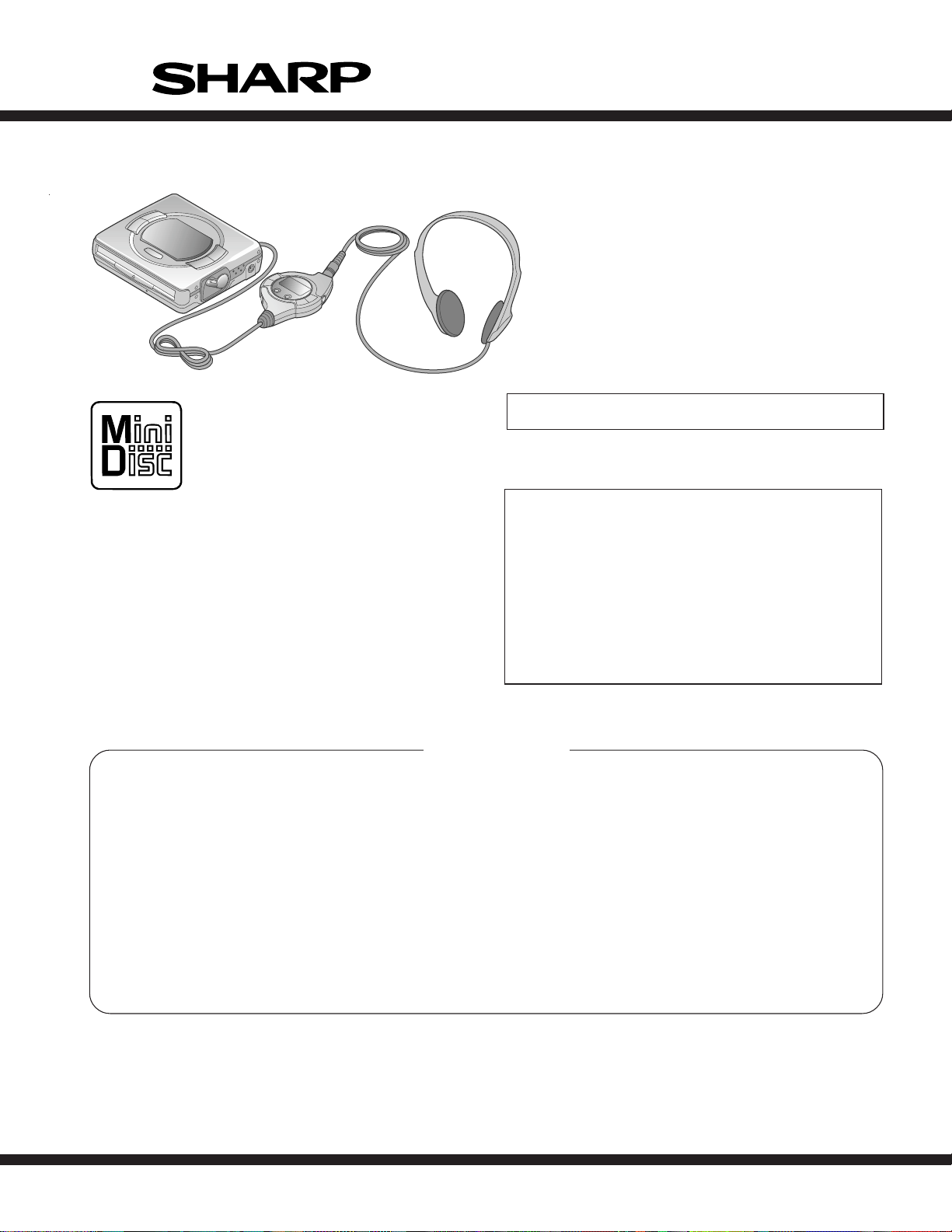
MD-S301MK
SERVICE MANUAL
No. S8865MDS301MK
MD-S301MK
• In the interests of user-safety the set should be restored to its original
condition and only parts identical to those specified should be used.
This Service Manual is for the MD-S301MK, which is a minormodification
model of the MD-S301, This manual, therefore, describes only the changed
points from the service manual. Please refer to the MD-S301 service manual
(No. S1801MDS301//) together with this manual.
MD-S301
Page
INSTALLING THE TOP CABINET .................................. 7
TEST MODE MENU ...................................................... 10
WAVEFORMS OF MD CIRCUIT................................... 31
TROUBLESHOOTING................................................... 32
FUNCTION TABLE OF IC ............................................. 36
CONTENTS
Page
SPECIFICATIONS ................................................................................................................................................................. 2
BATTERY DISPOSAL............................................................................................................................................................. 2
NAMES OF PARTS ............................................................................................................................................................... 3
OPERATION MANUAL .......................................................................................................................................................... 4
QUICK GUIDE ........................................................................................................................................................................ 6
DISASSEMBLY...................................................................................................................................................................... 7
REMOVING AND REINSTALLING THE MAIN PARTS......................................................................................................... 8
ADJUSTMENT ....................................................................................................................................................................... 9
BLOCK DIAGRAM ................................................................................................................................................................ 11
SCHEMATIC DIAGRAM/WIRING SIDE OF P.W.BOARD.................................................................................................... 12
VOLTAGE ............................................................................................................................................................................. 17
NOTES ON SCHEMATIC DIAGRAM ................................................................................................................................... 18
PARTS GUIDE/EXPLODED VIEW
SHARP CORPORATION
– 1 –
This document has been published to be used
for after sales service only.
The contents are subject to change without notice.
Page 2
MD-S301MK
FOR A COMPLETE DESCRIPTION OF THE OPERATION OF THIS UNIT, PLEASE REFER
TO THE OPERATION MANUAL.
SPECIFICATIONS
General
Power source:
Power consumption:7 W (AC adaptor)
Output power: RMS; 10 mW (5 mW + 5 mW)
Charging time: Approx. 3.5 hours
Battery life:
When using the
rechargeable battery
(fully charged)
included with the unit
Approx. 8 hours Approx.3.5 hours Approx. 11.5 hours
Volume level: "VOL 15"
The above values are the standard values when the unit is
charged and used at an ambient temperature of 68 ˚F (20 ˚C).
The playing time when using an alkaline battery may be different,
depending on the type and manufacturer of the battery and on the
operating temperature.
DC 3.6 V (rechargeable lithium-ion battery x 1)
DC 5 V (AC adaptor)
AC 120V, 60 Hz
DC 1.5 V: Optionally available battery case,
DC 4.5 V: Optionally available car adaptor,
(0.2 % T.H.D.)
(When using the AC adaptor included with
the unit)
When using one, commercially available, high
capacity, "AA" size, alkaline
battery (in the optionally
available battery case)
AD-S30BC(commercially available,
"AA" size, alkaline battery x 1)
AD-CA20X(
DC negative
system)
for cars with a 12-24V
ground electrical
When using one, commercially available, high
capacity, "AA" size, battery
with the rechargeable
battery (fully charged)
Output level:
Specified
output
Headphones — 5 mW + 5 mW 32 ohms
LINE 250 mV (-12 dB) — 50 kohms
Dimensions: Width: 3-7/16" (87 mm)
Height: 31/32" (24 mm)
Depth: 3-3/32" (78 mm)
Weight: 0.43 lbs. (192 g) with rechargeable
battery
Output socket: Headphones (impedance: 19 ohms)/
remote control unit
Maximum
output level
Load
impedance
MiniDisc Player
Type: Portable MiniDisc player
Signal readout: Non-contact, 3-beam semi-conductor
Audio channels: 2
Frequency response: 20 - 20,000 Hz (± 3 dB)
Rotation speed: Approx. 400 - 900 rpm
Error correction: ACIRC (Advanced Cross Interleave
Coding: ATRAC (Adaptive TRansform
D/A converter: 1 bit
Sampling frequency: 44.1kHz
Modulation system: EFM (Eight to Fourteen Modulation)
Wow and flutter: Unmeasurable (less than ±0.001%
laser pick-up
Reed-Solomon Code)
Acoustic Coding)
W.peak)
Specifications for this model are subject to change without
prior notice.
BATTERY DISPOSAL
Contains nickel cadmium (or sealed lead) battery.Must be
recycled or disposed of properly.Remove the battery from the
product and contact federal or state environmental agencies
for information on recycling and disposal options.
– 2 –
Page 3
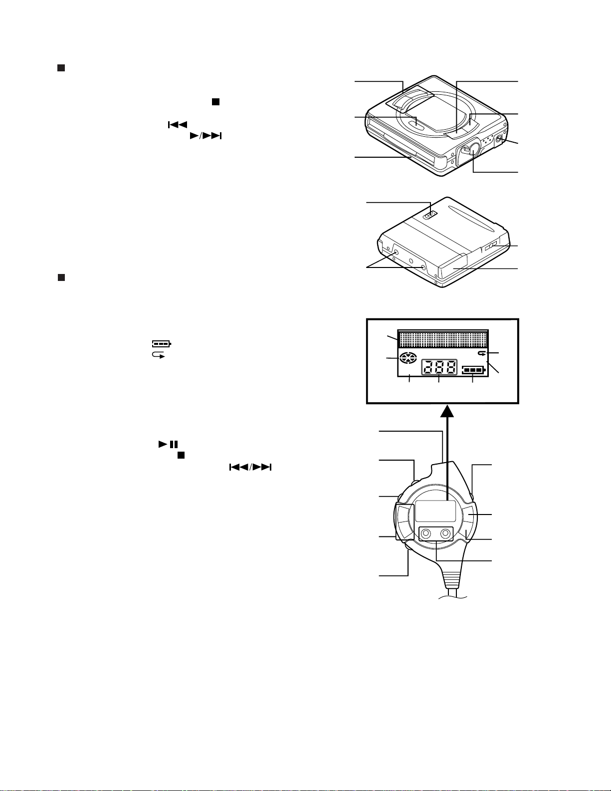
NAMES OF PARTS
Main unit
1. Volume Buttons: +, –
2. Stop/Power Off/Charge Button: :OFF
3. Power Indicator
4. Fast Reverse Button:
5. Play/Fast Forward Button:
6. 5V DC Input Socket
7. Eject Lever
8. Hold Switch
9. Battery Case Connection Terminals
10. Headphones Socket
11. Rechargeable Lithium-lon Battery Compartment
MD-S301MK
1
2
5
6
3
7
8
10
Remote control unit
1. Character/Time Information Display
2. Disc Mode Indicator
3. Total Track Number Display
4. Track Number Indicator
5. Battery Indicator:
6. Repeat Indicator:
7. Random Indicator
8. Headphones Socket
9. Hold Switch
10. Play Mode Button
11. Volume Buttons: +, –
12. Bass Button
13. Display Button
14. Play/Pause Button:
15. Stop/Power Off Button:
16. Fast Reverse/Fast Foward Buttons:
9
8
9
10
11
2
1
TOTAL
3
4
1
RANDOM
5
11
6
7
13
14
15
– 3 –
16
12
Page 4
MD-S301MK
■ Rechargeable battery power
When the rechargeable battery is used for
the first time or when you want to use it
after a long period of disuse, be sure to
charge it fully.
1Open the rechargeable battery com-
partment cover.
2Insert the rechargeable battery.
● Insert the side with the arrow first.
3Close the rechargeable battery com-
partment cover.
4Plug the AC adaptor into the AC outlet,
and then insert the plug on the AC
adaptor cord into the DC IN 5V jack.
5Press the ■:OFF button to begin charg-
ing.
● The POWER indicator will flash, and
the battery will begin charging.
● Battery charging will be complete in 3.5
hours. When the battery is fully
charged, the POWER indicator will go
out.
1
2
POWER SOURCE
Notes:
● After charging is complete, the AC
adaptor may be left connected.
(For example, when charging at night)
● The battery will not be charged when-
ever the power to the main unit is
turned on.
● If the operation in step 5 is performed
without inserting the rechargeable bat-
tery, the POWER indicator will flash for
5 seconds. This is normal.
● Do not force open the rechargeable
battery cover too far.
● Do not attach the optionally available
battery case when charging the internal
battery.
This unit can be used with 4 different power sources: a rechargeable battery, an AC
adaptor, an optionally available battery case (AD-S30BC), and an optionally available car
adaptor (AD-CA20X).
OPEN
OPEN
Mark
To the
DC IN 5V
jack
AC 120V, 60 Hz
OPEN
OFF
POWER
5
Insert
securely,
all the way
in.
4
■ Checking the remaining
amount of battery charge
The remaining amount of battery charge is
shown by t he battery indicator ( ) on
the remote control display during oper-
ation.
How to read the battery indicator
● When the battery is completely dis-
charged, the whole battery indicator will
flash. Recharge the battery or replace
the alkaline battery with a new one.
● When the battery has completely run
out, “Lo BATT” will appear in the dis-
play. Then, the power will be discon-
nected automatically.
Notes:
●
When the AC adaptor included with this
unit or an optionally available car adaptor
is used, the battery indicator will not be
shown.
●
The number of bars shown in the battery
indicator may increase or decrease, de-
pending on the operation being per-
formed. This is normal.
●
When the rechargeable battery and the
alkaline battery are used at the same time,
the rechargeable battery is used first, and
then the alkaline battery.
Since the battery indicator shows the re-
maining amount of the particular battery
being used, the number of bars will in-
crease when the unit switches to the al-
kaline battery.
CONVENIENT OPERATION OF THE UNIT
Battery
indicator
Charging is
needed.
When the battery is
completely charged
OPERATION MANUAL
– 4 –
Page 5
MD-S301MK
If trouble occurs
When this product is subjected to strong
external interference (mechanical shock,
excessive static electricity, abnormal sup-
ply voltage due to lightning, etc.) or if it is
operated incorrectly, it may malfunction. If
such a problem occurs, do the following:
1. Unplug the AC adaptor from the AC
outlet.
2. Remove the battery.
3. Leave the unit completely unpowered
for approximately 30 seconds.
4. Plug the AC adaptor back into the AC
outlet and retry the operation.
If strange sounds, smell or smoke come
out of the unit or an object is dropped into
the unit, remove the AC adaptor from the
AC outlet immediately and contact an au-
thorized Sharp service centre.
Many potential “problems” can be resolved by the owner without calling a service techni-
cian. If something seems to be wrong with this product, check the following before calling
your authorized SHARP dealer or service center.
PROBLEM CAUSE
The unit does not turn
on.
Is the AC adaptor disconnected?
Is the battery exhausted?
Is the unit in the safety mode?
Has condensation formed inside the unit?
Is the unit being influenced by mechanical shock or by
static electricity?
No sound is heard
from the headphones.
Is the volume set too low?
Is the remote control unit or the headphones plugged
in?
Are you trying to play a MiniDisc with data on it
instead of a MiniDisc containing music?
When the operation
buttons are pressed,
the unit does not
respond.
Is the unit in the safety mode?
Is the battery exhausted?
Is the remote control unit plug or the headphone plug
inserted firmly?
Has condensation formed inside the unit?
Is the unit being influenced by mechanical shock or by
static electricity?
Some sounds are
skipped.
Is the battery exhausted?
Is the unit being subjected to excessive vibration?
TROUBLESHOOTING
When an error message is displayed on the display, proceed as follows:
Display Meaning Remedy
BLANK
Nothing is recorded. Replace the disc with a
recorded disc.
E-DISC
The disc is damaged or
the music information is
not written properly on the
disc.
Replace the disc.
E-SYS
The unit is malfunctioning
and will require service.
For service, contact your
local Sharp authorized
servicer.
E-TEMP
The temperature is too
high.
Turn off the power, and
wait for a while.
E-TOC
E-UTOC
The disc is damagad. Replace the disc.
Lo BATT
The battery has run down. Charge the rechargeable
battery or replace the
alkaline battery (or use
the AC adaptor for power).
No DISC
A disc has not been
loaded.
Load a disc.
POWER?
Improper power is being
supplied.
Use one of the specified
power sources.
?DISC
There is an error in the
signal from the disc.
Replace the disc.
ERROR MESSAGES
– 5 –
Page 6
MD-S301MK
PORTABLE MINIDISC PLAYER Quick-Guide
MD-S301
MK
Guía rápida
AC power
Alimentación de CA
AC 120V, 60Hz
To an AC outlet
120V CA, 60Hz
A un tomacor rien te de CA
To the DC IN 5V jack
Al enchufe DC IN 5V
Alkaline battery power
Alimentación de la pila alcalina
1
• One alkaline battery
(LR6, “AA” size)
•
Una pila alcalina
(tamaño “AA”, LR6)
2
RELEASE LOCK
• Battery is not i ncl uded .
•
La pila no est á i n cl uid a.
Back of the M D pl ayer
Parte trasera del reproductor de minidiscos
Rechargeable battery power
Alimentación de la batería recargable
1
The optio nally avail able a lkali ne
battery case
La caja de la pila alcalina
disponible opcionalmente
Press the ■:OFF
3
2
OPEN
Volume Tone
Volumen Tono
OPEN
Sound control
Control del sonido
Volume level
Nivel de vol ume n
OPEN
AC 120V, 60Hz
To an AC outlet
120V CA, 60Hz
A un tomacor rien te de CA
(1) BASS 1
(2) BASS 2
(3) BASS 3
(4) BASS OFF
BASS
(1) BASS 1
(2) BASS 2
(3) BASS 3
● The volume level can be
adjusted from “0” to “30”.
●
El nivel de vol umen pued e
ajustarse desd e “0” a “30 ”.
(4) BASS OFF
4
button to begin
charging .
Pulse el bo tón
■:OFF
para iniciar
la carga.
Bass is emphasized a little.
Bass is emphasized more.
Bass is emphasized still more.
Bass emphasis is canceled.
Los graves se acentúan un
poco.
Los graves se acentúan más.
Los graves se acentúan toda-
vía más.
La acentuación de los graves
se cancela.
Loading and playing a MiniDisc
Connection
Connection
Inserción y reproducción de un minidisco
Conexión
Conexión
1
2
■ APSS
(Auto Program Search System)
■
APSS
(Sistema de bús queda
automática de programas)
■ Random play or Repeat play
■
Reproducción aleatoria o
reproducción repe tida
PLAY MODE
OFF
Track name
Nombre de pista
To move to the beginning of the next track:
Press the / ( ) button during playback.
To re-start the track being played:
Press th e butto n dur ing play back .
Para pas ar al pr inc ipi o de la pi sta sigu ient e:
Pulse el botó n
Para reiniciar la pista que se está reproduciendo:
Pulse el botón durante la reproducción.
During playback or while in the stop mode, press the PLAY
MODE but ton r epea ted ly to sele ct t he play back mod e.
..........
RANDOM
.............
.............
1
.........
No display
Durante la reproducción o en el modo de parada, pulse repetidamente el botón PLAY MODE para seleccionar el modo de
reprod ucción.
..........
RANDOM
.............
.............
1
...
Sin visualización
/()
durant e l a r e prod uc ci ó n.
Random play
Repeat play of all of the tracks
Repeat play of a single track
Normal playback
Reproducción aleatoria
Reproducción repetida de todas las pistas
Reproducción repetida de una sola pista
Reproducción normal
■ Important
●Do not wear your headphones when you are cross-
ing stree ts or near traff ic.
● Do n ot us e yo ur he ad phon es wh il e driv in g a mo t or
vehicle, it may create a dangerous traffic hazard
and may be illegal. Remember to obey all of the
safety rules in your area.
●Do not play the unit at a high volume. Hearing
experts advise against extended play at high volume levels.
●If you exper ience ring ing i n your e ars, reduce the
volume or discontinue use.
■
Importante
●
No se ponga auriculares cuando atraviese calles ni
cuando esté cerca del tráfico.
●
No emplee los auriculares mientr as conduce un
vehículo, porque puede cr ear situac iones peligr osas en el tráfico y puede ser ilegal. Recuerde que
debe respetar las reglas de seguridad de su zona.
●
No reproduzca sonido en el aparato a altos niveles
de volum en. Lo s exper tos di cen que es per judic ial
la repr oducc ión con tinuada a alto s nivel es de vol umen.
●
Si nota timbres en los oídos, reduzca el volumen o
no utilice el aparato.
■ Volume setting
Reduce the volume before starting to play. MiniDiscs,
compared to ordinary cassette tapes, have very little
noise. If the volu me is adjust ed according to your
usual exp ectations of noise, you may damage your
hearing due to the high volume.
■
Ajuste del volume n
Reduzca el volumen antes de iniciar la reproducción.
Los mínidiscos, en compara ción con las cintas de
casete normales, tienen muy poco ruido. Si se ajusta
el volume n de ac ue rdo co n el ruido que p ue de es pe rarse nor malment e, podría dañar se los oídos debido
al alto vol umen .
– 6 –
Page 7
DISASSEMBLY
MD-S301MK
Caution on Disassembly
Follow the below-mentioned notes when disassembling
the unit and reassembling it, to keep it safe and ensure
excellent performance:
1. Take the battery and minidisc out of the unit.
2. When disassembling the machine, be sure to withdraw
the power plug from the socket in advance.
3. When disassemble the parts, remove the nylon band or
wire holder as necessary.
To assemble after repair, be sure to arrange the wires as
they were.
If a screw of different length is fitted to the MD mecha-
nism (the screw of the part to be fitted to the MD
mechanism chassis), it may contact the optical pickup,
resulting in malfunction.
4. When repairing, pay due attention to electrostatic charges
of IC.
STEP
REMOVAL
1 Bottom Cover 1. Battery Cover.........(A1) x1 7-1
2 Top Cabinet 1. Screw.....................(B1) x4 7-1
3 Main PWB 1. Screw .................... (C1) x1 7-2
4 Mechanism Unit 1. Lift the back side, and 7-3
PROCEDURE
2. Screw .................... (A2) x6
2. Flexible PWB ........ (B2) x1 7-2
2. Flexible PWB ........ (C2) x2
3. Soldering ............. (C3) x3
remove in the arrow
direction.
FIGURE
Note:
Carefully handle the main PWB and flexible PWB.
So as to prevent electrostatic damage of optical pickup after
removing the flexible PWB (*1) for optical pickup from the
connector, wrap the front end of flexible PWB in conductive
aluminum foil.
(B1)x2
ø1x2.5mm
Center
Cabinet
(C2)x1*
Flexible PWB for
optical pickup
(A2)x2
ø1x2.5mm
Top Cabinet
Pull
(C2)x1
Bottom Cover
Figure 7-1
Pull
(C3)x3
Pull
Figure 7-2
(A2)x2
ø1x2.5mm
(A1)x1
Pull
(A2)x2
ø1x2.5mm
(B1)x2
ø1x2.5mm
(C1)x1
ø2x3mm
Main PWB
(B2)x1
Pull
Pull
Mechanism Unit
Figure 7-3
– 7 –
Page 8
MD-S301MK
(A2)x3
ø1.4x2.8mm
MD Mechanism
Spindle Motor
Solder joint of mechanism
flexible PWB
(A1)x1
REMOVING AND REINSTALLING THE MAIN PARTS
Remove the mechanism according to the disassembling methods 1 to 4. (See Page 7.)
How to remove the spindle motor (See Fig. 8-1.)
1. Remove the flexible PWB solder joint (A1) x 1.
2. Remove the screws (A2) x 3 pcs., and remove the spindle
motor.
* When installing the spindle motor, gently press in the arrow
direction (in view of grating).
How to remove the sled motor (See Fig. 8-2.)
1. Remove the stop washer (B1) x 1 pc., and remove the gear
(B2) x 1 pc.
2. Remove the screws (B3) x 2 pcs.
3. Remove the flex PWB soldering joint (B4) x 3 places, and
remove the sled motor.
Note:
Be careful so that the motor gear is not damaged.
(If the gear is damaged, abnormal sound is emitted when
searching is performed.)
Bracket
Sled Motor
Figure 8-1
(B3)x1
ø1.4x1.2mm
(B3)x1
ø1.4x1.5mm
Stop Washer
(B1)x1
(B2)x1
(B4)x3
Solder joint of mechanism
flexible PWB
How to reinstall the optical pickup unit
(See Fig. 8-3.)
1. Remove the screw (C1) x 1 pc.
2. Slowly raise the optical pickup.
Note:
Be careful so that the motor gear is not damaged.
(If the gear is damaged, abnormal sound is emitted when
searching is performed.)
Figure 8-2
(C1)x1
ø1.7x3mm
Optical Pickup
Shaft
Figure 8-3
– 8 –
Page 9
MD-S301MK
ADJUSTMENT
Preparation for adjustment (use the low reflection disc on which music has been recorded)
MD adjustment needs two types of disc, namely recording disc (low reflection disc) and Playback only disc (high reflection disc).
Type
1 High reflection disc MMD-110 (TEAC TEST MD) 88GMMD-110
2 Low reflection disc MMD-212 (TEAC TEST MD) 88GMMD-212
Test disc
How to enter the TEST MODE (In STANDBY state)
1
Holding down the PLAY MODE button of remote control unit, press the VOL button and button of main unit.
2
Charge control "ON"
3
Indication of microcomputer version for one second [ ]
: Microcomputer ROM version
: EEPROM version
4
All LCD lighting for 2 seconds
5
TEST MODE STOP "_TEST_"
* When the button is pressed while the indication 3 and 4 appears, the mode is changed to TEST MODE STOP state.
* If the button is pressed while indication 3 to 5 appears, the EEPROM rewrite-enable area is updated, and the mode is changed
to STAND-BY state.
How to leave the TEST MODE
1
In the TEST MODE STOP state, version indication state and full-lighting state press the button.
2
Initialization of normal mode setting.
(BASS setting, VOL setting, etc.)
3
EEPROM rewrite-enable area updating and adjustment error setting.
(all items are adjusted when power is turned on in the normal mode)
4
Change to standby state.
Parts No.
—
Preliminary automatic adjustment or EEPROM rewriting
1
Short-circuit TP435 and TP421.
2
Perform preliminary automatic adjustment or EEPROM rewriting.
3
Press the button to set the standby state.
4
Release short-circuiting of TP435 and TP421.
– 9 –
Page 10

MD-S301MK
EEPROM DATA LIST (ROM Version : h)
Focus setting
Item
F G 3 5 H F F 1 7 0 H
F F 2 F 0 H F H Z D B H
F L n 0 9 H D J G 1 4 H
F R V 0 0 H F P f 8 8 H
F L V 3 5 H W T f 2 0 H
F S S 0 2 H
Setting
Tracking setting
Item
T G 3 B H T F 1 7 0 H
T F 2 E 0 H T F S 0 0 H
T B o 1 9 H T B t 2 A H
T K o 1 F H T K t 1 1 H
T D o B B H T D t 1 E H
S C o 0 0 H S C t 4 0 H
S C m 5 3 H D B O 0 0 H
C L p 1 2 H C L r 2 4 H
W T m 9 0 H
Setting
Spindle setting
Item
S P G 1 6 H S P i A C H
S P m 8 5 H S P o 5 6 H
S P 1 1 0 H S P 2 6 0 H
S P 3 F 2 H S P 4 F 2 H
S P 5 1 0 H S P D 6 9 H
S P R 0 0 H
Setting
Sled setting
Item
S L K 4 2 H S T L 2 1 H
S T M 0 6 H S T E 2 1 H
S D V 6 6 H S J P 0 6 H
S R V 0 9 H
Setting
Item
Item
Item
Item
Setting
Setting
Setting
Setting
Adjustment setting
Item Setting
C O K A 0 H F A T C 0 H
T A T 3 E H C A T 2 0 H
F A B 0 0 H
Item
Digital EQ setting
Item
H Q 1 9 0 H H Q 2 9 0 H
H S G 1 1 H H S O F D H
L Q 1 9 0 H L Q 2 9 0 H
L S G 1 1 H L S O 0 0 H
G Q 1 9 4 H G Q 2 8 A H
G S G 1 1 H G S O 0 0 H
D Q R 0 0 H
Setting
Item
Control setting
Item Setting
C T O 4 7 H C T 1 D 0 H
P W L 0 3 H R C O 1 B H
R C 1 0 0 H D R E 6 E H
D R 1 1 0 H D R 2 4 6 H
I N 1 3 2 H I N 2 4 9 H
I N E 6 E H C T 2 1 4 H
C T 3 8 0 H C T 4 0 0 H
C T 5 0 0 H C T 6 0 0 H
C T 7 0 0 H
H: After measuring temperature set the value obtained
from the correction table.
TEST mode version display:
: Microcomputer ROM version
: EEPROM version
: Destination setting
Item
Setting
Setting
Setting
BASS setting
Item Setting
B S 1 A 2 H B S 2 C 4 H
B S 3 E 4 H
Item
TEMP setting
Item
T M H
Setting
Setting
– 10 –
Page 11

26~29
32~37
39~46
25
41
74
42
40
28, 30
73
67, 44
+2.5V
Q852
IC404
REMOTE CONTROL
DRIVER
5, 6
IC101
IR3R55
RF SIGNAL
PROCESSOR
Q101
15
1~9
11~19
IC201
LR376481
ENDEC
3, 5~9, 11
74, 70~72
48~55
37~39
90~100
64
65
97
43
SW452 SKIP DOWN
SW453 STOP
SW454 VOLUME DOWN
SW455 VOLUME UP
17~22, 24
IC601
MPC17A39
PICKUP COIL
DRIVER
2, 15~18, 20, 21
17
24
13
1, 3, 6
20, 19
3-PHASE BRUSH
LEESS DRIVER
IC901
BA6965FV
6, 8, 11, 12
4MBIT D-RAM
DRIVER CONT
M
M
M901
SPINDLE MOTOR
A-B SIGNAL
E-F SIGNAL 11, 12
9, 10
1, 2, 3, 4
RF1~RF4 SIGNAL
OPTICAL
PICKUP UNIT
BAE
F
TRACKING
LASER DIODE
FOCUS
RF1
RF2
RF3
RF4
J701
REMOTE CONTROL/
HEADPHONES
L-CH
R-CH
18
19
17
+B+B
70
AUDIO AMP
IC702
IR3R54N
14
16
2, 4
7, 16
22, 23
24
+B
5, 11
15
1, 2, 3, 6
D/A
CONVERTER
IC501
UDA1320
10
7, 5, 3
1~4
4
5
IC403
TC7W14FU
INVERTER
EEPROM
IC402
S29L294A
+B+B
88
11, 1486~88
+B
9, 23, 24
36, 81
IC401
IX2677AF
SYSTEM
MICROCOMPUTER
91, 16~19
82~84, 86
XL201
33.8688MHz
SW401
HOLD SW
SW901
DISC IN
SW451 PLAY/SKIP UP
ENDEC
AUDIO
D/ACONVERTER
LASER
MOTOR DRIVER
12, 33, 72
IC405
S80821LN
RESET
D402
+B
+B
4
2
1
15
POWER DRIVE
IC831, IC832
IC821, IC851
IC871
TK71325M
POWER SUPPLY
MICROCOMPUTER
4
2, 3
5
SYSTEM MICROCOMPUTER
MOTOR DRIVE
CHARGE DRIVE
ON/OFF
D801 Q801
CONSTANT
CURRENT DRIVE
IC812
IC861,
862, 863
START UP DRIVE
2~4
INTERNAL
BATTERY
3.6V
BATTERY
1.5V
1
J801
EXTERNAL BATTERY
DC JACK
(DC IN 5V)
+B
12, 62, 68,
78, 87
IC202
IX2567AF
4M BIT
D-RAM
20
+B
10
+B
5, 9, 10, 14
23, 27, 28, 32
1, 4, 7, 12, 19,
22 , 25, 30, 33
1015
+B
LASER POWER
CONTROL
M902
SLED MOTOR
MD
+B
13, 14, 24, 42 18, 19, 43
1
2
4
25~30, 40
4,13~16
38, 60, 63
9, 88
2~7
SLED MOTER
DRIVER
4, 7, 8
9, 13
8, 10, 12
57
90
S-80821ALNP
Q871
LRAGND
DGND
KEY
PLAY
DATA
EL+B
2
3
4
5
1
7
8
6
U.V.W
U.V.W
IC911, 912, 913
Q901 ~ Q906
POWER SELECT CHARGE
7SH86FU
MD-S301MK
Figure 11 BLOCK DIAGRAM
– 11 –
Page 12

MD-S301MK
1
4
3
4
0
T
T
9
K
W
A
B
C
TP102
TP101
TP103
TP105
3 2
4
1
R903
150
R420
A
R905
100K
330
5
4 3 2 1
5
B
COM
LDYCC
R906
C903
1
R419
100K
CN101
FLEXBLE
PWB
D
E
F
PLAYBACK SIGNAL
C102
1
C103
@
1
R101
390K
RF SIGNAL
PROCESSOR
TP106
6
7
6
7
DGND
DGND
270K
TP616
TP614
TP108
8
8
LDON
TP109
9
9
LDVAR
R909
10K
C902
0.01
BA6965FV
FG
11
12
BRK+
13
14
STBY
RIB
15
VCC
16
17
18
19
VOUTVMUOUT
20
BRUSH LEESS
TP110
10
11
11
10
RF2
IC901
C911
0.1
3-PHASE
DRIVER
TP113
TP111
13
14
12
14
13
12
MP/R
AGND
OPICVCC
PICKUP UNIT
GND
CSLBRK–
CSL
CST
COM
WIN
VIN
UIN
RFWOUT
TP115
TP114
16
15
16
15
RF4
RF3FRF1
OPTICAL
10
9
8
7
6
5
4
3
2
1
TP116
TP117
18
17
18
17
E
R908
100K
C910
0.047
1
R902
TP119
TP118
19
19
T+
R907
150K
C909
0.047
C908
0.47
C905
0.0022
C906
0.0022
R904
TP120
21
20
21
20
T–
E–
NDS355AN
1
R901
22K
IC101
IR3R55
C161
1
TP121
TP122
22
22
E+
Q901
U
V
W
C907
0.0022
TP144
C104
0.027
Q101
2SA17457
S
R911
100K
D
S
Q904
NDS335N
IC911
RN4904
IC912
RN4904
IC913
RN4904
C112
0.033
48
ROUT
RF1
1
R
RF2
2
and
RF3
3
SW
RF4
4
REFI
5
6
REFO
RFADD
7
TCGI
8
AIN
9
BIN
10
EIN
11
FIN
12
BIAS
13
Q902
NDS355AN
G
S
R912
100K
D
G
S
R914
100K
1
6
2
5
4 3
6
1
5
2
4 3
6
1
2
5
4 3
IC911~IC913’
POWER SELECT
CHARGE DRIVER
R413
1K
47
GOUT
14
R915
100K
AVCC
C111
0.0033
CK112
46
45
TTR
EFMAGI
DIFF
DIFF
BIAS
STBY
16
15
CK101
R154
1.2K
F–
T+
F+
T–
NDS355AN
G
Q905
NDS335N
G
CK902
CK903
44
EFM
AGC
EFMAGC
DISC
17
CK103
CK102
Q903
D D D
S
R913
100K
D
S
R916
100K
CK901
C110
SGAIN
C113
0.1
G
G
0.22
42
43
AGND
LOGIC
AGND
18
19
Q906
NDS335N
C109
AVCC
ADIP
AGC
DGND
41
LPF
20
4.7
EFMI
DTEMP
40
NC
21
CK104
TP145
C107
0.012
39
RF2-1
EFMO
HPF
LATCH
22
CK105
38
ADAG
CLOCK
23
CK106
TP433
R434
37
ADIPI
ADAGC
ADLPFO
TCGO
BOUT
EOUT
FOUT
DATA
24
TP434
1K
R430
10K
ADIPO
22KO
22KI
WBO
AOUT
DVCC
C106
0.22
NC
1
2
3
4
TP139
36
35
34
33
32
31
30
29
28
27
26
25
TP131
TP100
R433
1K
IC402
S29L294A
VCC
CS
SK
DO
PRTCT
GND
DI
2
EEPROM
CK111
CK109
CK108
CK107
TP133
TP132
R112
22K
R111
22K
TP130
R431
100K
8
6
5
TP436
R102
56K
CK110
C121
7
R114
22K
R113
22K
270P(CH)
C122
270P(CH)
R161
C165
0.033
TP435
1K
R435
R414
22K
EFM
TCG
1.2K
WB
C123
A
B
E
F
C124
390P
390P
17
CK205
CK206
CK207
C203
0.1
R204
1K
TP210
CK201
CK203
CK204
FOK
SENSE
CIN
DINT
XRT
SYSD0
SYSD1
SYSD2
SYSD3
SYSD4
SYSD5
SYSD6
SYSD7
SYWRX
SYRDX
SYCS
CIN
TP209
TP417
TP418
TP409
TP410
R222
1M
TP208
74
73
75
72
66
70
68
69
71
67
BCLK
LRCK
VDD3
DFCK
DGND
DOUT
ADDATA
DADATA
TOTMON
76
TEMON
77
78
SBCK
LR376481
98
SYWRX
99
SYRDX
100
SYRS
EFMI
AVCC
TCG
AGND
AIN
FIN
EIN
BIN
10
8
9
6
5
4 3 2
7
EFM
F
B
TCG E WB
A
R231
82K
R233
270K
LED401
CL200HRC
1K
R423
66
70
68
69
71
72
EMPH
SYSTEM MICROCOMPUTER
SLCNT2
4
P57
VSS
76
77
78
SLCNT4
SLCNT3
5
P56
HSTOP
NC P64
NC
98
99
100
SLCNT5
6
7
P54
P55
P65
INNSW
VBATC
PDCNT
OEM
SLCNT6
8
67
9
65
PWLED
PBOPON
IX2677AF
X2
VDD
10
11
100K
R405
C204
0.1
TP201
76
77
78
79
80
81
82
83
84
85
86
87
88
89
90
91
92
93
94
95
96
97
98
99
100
76
77
78
79
80
81
82
83
84
85
86
87
88
89
90
91
92
93
94
95
96
97
98
99
100
75
P66
P67
VDD
SPIN
P101
TEST0
TEST1
EPCS
EEPD
EEPK
P33
ELON
CIN
PHOLD
PCNT1
VPP
PCNT2
CKSTP
DISCIN
FEMON
SBO
SBSY
SFSY
FOK
SENSE
COUT
MCCK
DINTX
VDD1
DGND
RSTX
SYSD0
SYSD1
SYSD2
SYSD3
SYSD4
SYSD5
SYSD6
SYSD7
EFMMON
1
74
P62
HPLAY
SLCNT1
R232
62K
73
3 2 1
TP421
33.868MHz
64
65
63
X1I
DIN
X1O
IC201
ENDEC
VBAT
WBI
VDD1
11
1312
C231
0.1
TP414
62
63
64
PBLAT
RACLK
RADAT
IC401
XT2
VSS
X1
14
13 12
TP422
XL201
61
62
VDD1
DGND
TEST0
DGND
15
14
TP218
TP219
10/6.3
60
60
RFLAT
OPICGA
RESET
XT1
16
15
CK403
VPD
TEST1
C101
LDON
28
27
26
DINT
DINT
5P(CH)
60
59
VXI
50
49
48
28
27
26
TEST2
16
17
X176KO
58
59
P43
50
49
RKEY
PLVDRY
PLVDCI
SENSE
18
17
SENSE
FOK
C211
5P(CH)
58
57
CDBCLK
CDLRCK
EFMO
PLCK
ACRCER
RAA1
RAA2
RAA3
FODRF
X176KO
19
18
FODRF
L101
10µH
57
56
PSLDCI
PSLDRY
SYD2
SYD1
XRT
FOK
19
20
XRT
R411
100K
C212
56
55
TEST4
CDDATA
FODRR
TRDRF
20
21
TRDRF
FODRR
SYSD7
54 53
55
SYD7
PSLINN
PO4
PO5
21
22
C222
22P(CH)
53
54
TEST3
TES01
RARASX
RACASX
TRDRR
SLDRF
23
22
SLDRF
TRDRR
SYSD6
SYSD5
52
SYD6
SYD5
SYD0
BEEP
KHOLD
RPLAY
RMDAT
RMLOG
SYRS
SYRD
SYWR
AVREF1
MDOUT5
LDVAR
AVSS
CNTRY
TEMP
HKEY1
DCNT
AVDD
24
23
C407
52
EX1
EX0
TCRS
RAD0
RAD1
RAWEX
RAA9
RAD3
RAD2
DGND
RAOEX
RAA8
RAA7
RAA6
RAA5
RAA4
VDD2
RAA10
RAA0
SLDRR
SPDRF
24
25
SPDRF
SYSD4
SYSD3
51
SYD3
SYD4
P27
P26
P25
ANI5
PLVINN
AVREF0
25
TP411
1
51
X700KO
SPDRR
C201
50
49
48
47
46
45
44
43
42
41
40
39
38
37
36
35
34
33
32
31
30
29
28
27
26
50
49
48
47
46
45
44
43
42
41
40
39
38
37
36
35
34
33
32
31
30
29
28
27
26
1
SYSD2
SYSD1
SYSD0
TP413
SYCS
SYRDX
SYWRX
TP419
TP220
L201
CK406
CK405
CK404
22K
R408
TP205
TP204
TP203
TP206
4.7µH
S
R407
TP412
R40
22
C
0.
100K
R
3
TP606
TP605
6
5
6
5
U
COM
TP607
8
7
8
7
W
U
TP608
TP609
9
9
V
V
MOTOR
TP610
10
11
10
11
U
V
M901
SLED
W
1
M
3
V
TP611
TP612
13
12
13
12
W
COM
1
3
M
4
2 4
COM
M902
SPINDLE
MOTOR
W
U
TP613
CN601
2
COM
C603
X176KO
1
2
3
R601
4
56K
L601
5
47uH
T+
T–
F+
1
C601
1
1
C604
6
L602
7
47µH
8
9
L603
10
47µH
F–
11
L604
12
47µH
13
14
TRDRR
15
TRDRF
16
FODRF
17
FODRR
18
C602
1
PICKUP COIL DRIVER
CLK
PS
OE
VD1
FO1
PGND
PGND
RO1
VD1
VD2
RO2
PGND
PGND
FO2
VD2
RI1
FI1
FI2
RI2
IC601
MPC17A39
36
VC
35
34
LG
GND
33
VD3
32
FO3
31
30
RO3
29
VD3
28
VD4
27
26
RO4
25
FO4
24
VD4
23
RI3
22
21
FI3
SPDRF
FI4
20
RI4
19
VG
AGND
TP601
TP603
TP604
TP602
4 3 2 1
4 3 2 1
G
MECHANISM
FLEXIBLE PWB
PH901
SW901
DISC IN
SPINDLE MOTOR/SLED MOTOR UNIT
GP1S93K
H
• NOTES ON SCHEMATIC DIAGRAM can be found on page 18.
1
23456
Figure 12 SCHEMATIC DIAGRAM (1/2)
C622
0.1
L609
10µH
TP617
C600
15/10
L608
47µH
SLDRF
– 12 –
L600
2.2µH
C608
1
TP615
C609
4.7
C408
IC403
TC7W14FU
INVERTER
R402
15K
1
R416
12K
10P(CH)
C409
R417
10K
C405
150P(CH)
8
7
R455
100K
R415
47K
KEY FLEXIBLE
39K
PWB
SW455
V.UP
R451
12K
SW454
10K
R424
6
5
R418
4 3 2 1
C406
680P
TP401
TP402
TP403
2
3
1
2
1
SW453
V.DOWN
TP404
4
4 3
STOP
R452
TP405
TP406
5
6
6
5
SW452
S.DOWN
10K
CN401
R454
22K
SW451
PLAY/S.UP
KEY SWITCH FLEXIBLE UNIT
Page 13

10K
22K
TP205
TP204
TP203
TP206
TP220
L201
4.7µH
+2.5V
IC202
IX2567AF
4BIT D-RAM
I/O1
1
I/O2
2
WE
3
RAS
4
A9
5
A0
6
A1
7
A2
8
A3
9
VCC A4
10
TP202
C202
1
L202
1µH
MD-S301MK
MAIN PWB-A
L701
R713
161514 13
8
9
C701
1
C707
0.056
C706
3.3/6.3
C713
R711
82
10
0.22
R707
8.2
R714
8.2
R712
11
C702
27K
C714
0.22
82
R708
27K
12
1
C715
0.083
L-CH
R-CH
C716
0.083
D451
015Z5.1Y
C751
0.1
L751
4.7µH
L732
L731
L733
L736
L710
L734
TP728
TIPSOLID INDUCTI
R722
TP725
D702
015Z5.1Y
TP724
TP723
TP722
TP721
TP726
TP727
4
3
2
1
6
5
7
8
J701
REMOTE CONTROL/
HEADPHONES
L-CH
R-CH
AGND
DGND
KEY
PLAY
DATA
EL+B
47µH
R709
C711
R710
C703
1
C704
C705
0.01
24
22
23
AUDIO AMP.
1K
1K
1
R701
150K
19
20
21
IC702
IR3R54N
4 3 2 1
6
5
0.0022
L702
47µH
18
R702
330K
0.0022
7
C712
17
GND
20
I/O4
19
I/O3
18
CAS
17
OE
16
A8
15
A7
14
A6
13
12
A5
11
C504
10/6.3
C742
0.001
C741
0.01
+2.2V
IC501
UDA1320
D/A CONVERTER
-2.2V
VOUTR
BCK
1
VSSA
WS
2
VOUTL
DATA
3
VDDA
VDDD
4
VREFD
VSSD
5
MUTE
SYSCLK
6
DEEM
APSEL
7
SF0
SF1
8
TP501
L721
100µH
16
C502
15
10/6.3
14
13
12
11
C503
10
10/6.3
9
C508
L501
10µH
2.2
C501
10/6.3
TP701
C859
1
2.2
C507
L711
100µH
R501
R502
47/4.0
C732
47/4.0
5.6K
5.6K
R506
8.2K
C722
TP702
47/4.0
C731
47/4.0
R505
8.2K
C721
+2.5V
D841
1SS372
C846
C845
1
1
IC802
UMD3N
CONSTANT
C821
0.1
TP812
+2.5V
330K
C816
27P(CH)
6
5
EAOUT
GND
0.33
OUT
VCC
8
7
C838
R854
100K
100K
R870
R869
100K
Q861
2SC4738 GR
1
C864
1
R864
100K
R821
56K
R822
27K
C828
12P
4
5
(CH)
VCC
R824
390K
GND
2 1
3
IC833
TC7S66FU
ANALOG SWITCH
R842
100K
C837
180P(CH)
10K
R838
R840
4 3 2 1
+ –
EAIN+
EAIN–
++
–
PWM
OSC
STATE
ROSC
OSCOUT
11
10
9
C839
560P
15K
0.01
R843
C852
IC851
1
NDC631N
POWER DRIVE
1
2
3
D862
HZU2BLL
R868
C857
1M
10/10
1
2
R863
3
100K
C863
0.01
IC862
TC7SL32FU
START UP DRIVE
R823
C826
360K
DB
6
5
4
1
L824
10µH
D822
F1J2F
C827
10
R825
18K
R835
100K
R836
R839
100K
100K
33K
VREF
OSCIN
12
C840
390P
2.8V DC/DC CONVERTER
1
2
3
5
4
0.01
C836
IC832
C833
IR3M09N
0.01
POWER DRIVE
C830
L852
4.7µH
L851
10µH
C851
3.3
IC852
S8327B28
5
4
C862
R867
3.3
390K
R862
470K
D831
1
R861
C815
27P(CH)
6
GND
RB521S30
OUT
7
G
R851
100K
SB10015C
1K
R860
100K
START UP DRIVE
IC821
NDC631N
POWER DRIVE
1
6
2
5
4
3
C832
220P(CH)
5
4 3 2 1
EAOUT
EAIN–
EAIN+
++
–
PWM
STATE
VCC
10
8
9
R837
15K
D
Q852
2SJ305
S
D854
D
G
S
Q853
NDS335N
5
1
2
4
3
IC861
TC7SL32FU
ROSC
+
–
R833
33µH
C853
L822
4.7µH
L823
4.7µH
C824
3.3
D821
RB521S30
33K
10K
R831
DB
OSC
OSCOUT
11
12
C834
L853
1
C861
1
4
5
6
R832
100K
VREF
560P
OSCIN
C835
390P
R852
1K
3
2
1
IC831
L821
1µH
C822
33/10
0.01
C831
IR3M09N
POWER DRIVE
D2
D1
D0
SW401 HOLD
K406
K405
K404
413
S
DX
RX
9
R407
TP412
R409
22K
R401
330K
C403
0.047
100K
R412
150K
TP416
TP415
D402
1SS361
R403
TP408
10K
7SH86FU
REMOTE CONTROL
1
2
IC405
S80821LN
RESET
1
2
IC404
4
3
5
4 3
R871
Q871
2SA1745
1K
C871
0.47
L871
4.7
+2.5V
IC871
TK71325M
22K
R454
CN401
LE UNIT
SW451
PLAY/S.UP
POWER
SUPPLY
MICROCOMPUTER
+2.5V
C401
10/6.3
R865
100K
R866
100K
R421
1K
R422
1K
START UP DRIVE
TP811
C611
R847
220K
C842
56P(CH)
R845
240K
R844
270K
D856
C858
10
C856
D857
RB491D
1
2
3
4
5
D861
1SS393
1
5
2
3
4
IC863
TC7SL00FU
L102
10µH
C151
68/10
L611
1µH
1
C855
L854
F1J2F
10µH
1
RB521S30
3 2 1
R846
C841
1
D855
C865
CURRENT DRIVE
6
1
1
C823
R814
100K
R819
100K
Q812
DTC144 EE
Q851
G
2SJ305
D S
D814
RB521S30
D852
1SS372
IC815
RN4986
CHARGE DRIVE
D802
015Z5.1Y
2.7K
R801
CURRENT DRIVE
R803
4
5
3.9K
2
3
R804
1.2K
D812
SB10015C
IC812
HAT1025R
8
1
2
7
6
3
4
5
CONSTANT
CURRENT DRIVE
D813
SB10015C
Q811
DTC144 EE
POWER SELECT
CHARGE DRIVE
D851
RB521S30
C813
1
TP805
IC801
HN1C03FU
CONSTANT
1
2
3
6
1
2
5
4
3
IC814
RN4904
C801
1
R802
3.3K
D803
6
5
R805
4
10K
R806
D811
SB10015C
8
6
7
1
2
3
R813
100K
C812
0.1
270
TP803
1
2
TP112
3
RB521S30
TP806
R811
1K
5
R812
22K
4
C811
IC811
1
NDH831N
CONSTANT
CURRENT DRIVE
TP801
R817
470K
R818
560K
TP802
J801
DC JACK
TP804
Q801
2SD1950
TP871
TP872
+
EX
BATTERY,
–
EX
BATTERY
+
CHARGE
–
CHARGE
+
,–
,+
,–
• The numbers 1 to 17 are waveform numbers shown in page 31 of MD-S301.
7
8 9 10 11 12
Figure 13 SCHEMATIC DIAGRAM (2/2)
– 13 –
Page 14

MD-S301MK
A
B
C
9
R501
R502
D
R506
8
17
E
36
F
G
118
R601
R868
R869
D854
L853
C503
R505
C502
C611
L611C622
L609
3035 25 20
IC601
5
Q853
C609
L601
C601
L702
10
C507
C508
R870
IC871
9
16
C608
L608
C602
L701
IC852
D862
13
C857
R702
10
15
15
L602
C603
C853
C401
5
IC501
L600
C600
19
C604
45
C731
L603
L501
Q861
8
1
D402
R420
C504
C408
R419
C204
C856
C855
C858
L604
C706
R232
R231
C741
C501
C203
C732
76
100
C231
J701
REMOTE CONTROL/
HEADPHONES
J701
C722
D857
C721
L721
L851
R222
65 60
L101
L854
XL201
C211
C212
55
R113
R114
C101
C151
D856
L201
75
R233
C851
C201
80
85
90
95
1
LED401
L711
L852
70
IC201
51015
C121
C122
C123
C124
L102
D822
20
R825
R112
C109
1
3
C106
L824
IC833
51
45
40
35
30
25
R806
1
6
4
IC802
C822
L822
L823
C824
C813
5
4
50
10 11
C202
26
R111
37
C107
48
C110
C111
L821
C827
Q801
C841
1
5
6
L202
C407
3035
40
IC101
45
510
112
C112
C103
C102
C801
C104
R802
R871
IC202
2536
20
15
C161
R101
R803
R805
D813
24
13
D803
J801
6
Q871
Q101
C871
26
16
15
C113R154
R801
334
IC801
1
R804
D802
J801
DC JACK
1
MAIN PWB-A(BOTTOM VIEW)
• : Through-hole where the top, bottom and +B patterns are connected.
H
• : Through-hole where the top, bottom and hround patterns are connected.
• : Through-hole where the top and bottom patterns are connected.
• The numbers 1 to 17 are waveform numbers shown in page 31 of MD-S301.
1
23456
Figure 14 WIRING OF P.W.BOARD (1/3)
– 14 –
Page 15

IC401
R430
R434
1
45
8
R435
R433
R431
R102
R414
R403
R407
R916
IC913
Q903
R413
Q902
Q901
R911
IC911
R913
R912
1
3
4
6
1
3
4
6
1
3
4
6
IC912
R915 R914
C903
R903
R908
R907
R905
R906
Q904
Q905
Q906
R405
R418
C406
IC403
R411
R204
R417
R416
R423
1
25
26
30354045
50
51
55
60
65
70
75
76 100
80 85 90 95
5
10
15
20
C165
R161
IC404
R409
C823
C812
R818
R817
C821
R822
R821
R844
C831
R832
R835
R823
C836
C828
R839
R842
R847
C842
R845
R408
R412
C815
R838
R840
C837
C816
R824
R831
R833
C830 C826
C403
1
45
8
IC405
R865
R424
R866
R402
C859
1
5
10
12
13
24
15
20
C701
R707
C707
R708
C702
C405
C742
R415
R401
R422
R862
1
3
1
3
4
4
455
4
5
1
3
4
5
1
2
4
3
R864
C864
R452
R455
R451
R454
R860
R867
R861
R863
C863
IC862
IC861
IC863
IC815
C852
C409
R909
C902
C909
C910
C908
R701
C705
C704C703
R709
R710
C713
C714
R711
R712
C711
C712
R714
L751
R852
C861
C862
D861
C838
D855
R843
C839
R851
R732
R731
R722
C715
C716
D702
IC851
D821
R836
D451
L710
L734
L733
Q851
L871
C846
C845
IC821
D841
D812
C833
R837C835
C834
1
1
1
4
8
5
1
13
3
6
6
6
7
7
12
12
C840
D831
Q852
C865
D852
R854
C751
L736
R421
R713
D811
1
4
5
6
IC814
R813
Q812
113
3
1
3
4
4
6
6
4
6
Q811
R812
C811
R819
R814
D851
D814
R811
R846
C832
SW401
CN401
CN601
CN101
IC702
IC402
IC901
IC831
IC832
IC812
IC811
C911
C905
C906
C907
R904
R902
R901
1
10
11
15
20
5
KEY SWITCH
FLEXIBLE UNIT
BATTERY,–
(206)
PICKUP
FLEXIBLE PWB
MECHANISM
FLEXIBLE PWB
SW401
HOLD
MAIN PWB-A(TOP VIEW)
BATTERY,+
(207)
EXT.BATTERY
(220)
2
3
4
5
7
6
12
13
14
15
11
10
16
TP433
TP102
TP103
TP100
TP101
TP144
TP105
TP120
TP118
TP117
TP121
TP122
TP119
TP811
TP115
TP113
TP116
TP114
TP111
TP109
TP436
TP602
TP610
TP612
TP613
TP603
TP408
TP871
TP609
TP607
TP615
TP606
TP608
TP617
TP611
TP139
TP604
TP201
TP410
TP614
TP616
TP110
TP418
TP605
TP601
TP417 TP133
TP131
TP202
TP435
TP132
TP434
TP130
TP414
TP108
TP413
TP205
TP206
TP203
TP419
TP415
TP409
TP416
TP805
TP411
TP204
TP219
TP404
TP209
TP210
TP208
TP220
TP218
TP501
TP702
TP422
TP701
TP402
TP872
TP802
TP421
TP106
TP403
TP406
TP401
TP405
TP812
TP725
TP112
TP412
TP801
TP724
TP803
TP728
TP727
TP804
TP145
TP722
TP721
TP806
TP726
TP723
1
13
CK108
1
22
P16 5 - C
P16 5 - H
P16 3 - E
7
Figure 15 WIRING OF P.W.BOARD (2/3)
8 9 10 11 12
– 15 –
MD-S301MK
Page 16

MD-S301MK
A
SPINDLE MOTOR
B
C
D
M901
SW901
DISC IN
MECHANISM
FLEXIBLE PWB
M902
SLED MOTOR
P15 10 - A
TO MAIN PWB
CN401
VOLUME
UP
SW455
E
CN601
REW
SW452
P15 10 - G
TO MAIN PWB
SW451
SW454
PICKUP UNIT (15)
VOLUME
DOWN
SW453
PLAY/FF
:OFF
F
STOP
KEY SWITCH
FLEXBLE UNIT(221-9)
G
FLEXIBLE
PWB
P15 8 - G
CN101
TO MAIN PWB
H
1
23456
Figure 16 WIRING OF P.W.BOARD (3/3)
– 16 –
Page 17

VOL TAGE
MD-S301MK
PIN
NO.
1
2
3
4
5
6
7
8
9
10
11
12
13
14
15
16
17
18
19
20
21
22
23
24
25
26
27
28
29
30
31
32
33
34
35
36
37
38
39
40
41
42
43
44
45
46
47
48
IC101
VOLTAGE
0.71V
0.71V
0.71V
0.71V
1.27V
1.27V
0.71V
1.27V
1.28V
1.28V
1.27V
1.27V
2.53V
2.53V
0V
2.53V
2.53V
0V
0V
1.48V
2.51V
0V
0V
2.53V
1.27V
1.27V
1.28V
1.28V
1.27V
1.39V
1.27V
1.27V
1.28V
0V
1.27V
0V
0V
1.27V
1.27V
1.28V
1.27V
2.53V
0V
0V
1.27V
0V
1.27V
0V
PIN
NO.
1
2
3
4
5
6
7
8
9
10
11
12
13
14
15
16
17
18
19
20
21
22
23
24
25
26
27
28
29
30
31
32
33
34
35
36
37
38
39
40
41
42
43
44
45
46
47
48
49
50
VOLTAGE
0.94V
2.53V
1.28V
0V
1.27V
1.27V
1.27V
1.27V
1.27V
2.22V
1.38V
2.03V
0V
0V
0V
0V
1V
0V
0V
0V
0V
0V
0V
0V
0V
0.5V
0.6V
0.58V
1.4V
0.92V
2.54V
0.6V
0.99V
0.99V
0.81V
0.8V
1.82V
0V
2.07V
1.62V
1.67V
0.92V
1.74V
2.53V
1.7V
1.52V
0V
1.94V
1V
0.92V
IC201
PIN
NO.
100
51
52
53
54
55
56
57
58
59
60
61
62
63
64
65
66
67
68
69
70
71
72
73
74
75
76
77
78
79
80
81
82
83
84
85
86
87
88
89
90
91
92
93
94
95
96
97
98
99
VOLTAGE
1.01V
0V
0V
0V
0V
0V
0V
0V
0V
0V
0V
2.03V
0V
0.9V
0.8V
0V
0V
2.02V
0V
1V
1V
1V
0V
0V
1V
1V
1V
2.02V
0V
2.02V
1V
2.02V
0V
0V
1V
2.02V
2.02V
0V
2.5V
0V
0V
0V
0V
0V
0V
0V
0V
2.51V
2.5V
0V
PIN
NO.
10
11
12
13
14
15
16
17
18
19
20
1
2
3
4
5
6
7
8
9
IC202
VOLTAGE
0V
0V
2.41V
0V
1.13V
1.4V
0.58V
0.6V
0.6V
2.54V
0.62V
0.8V
0.8V
0.8V
0.8V
1.82V
1.96V
1.3V
1.7V
0V
PIN
NO.
1
2
3
4
5
6
7
8
9
10
11
12
13
14
15
16
17
18
19
20
21
22
23
24
25
26
27
28
29
30
31
32
33
34
35
36
37
38
39
40
41
42
43
44
45
46
47
48
49
50
VOLTAGE
2.52V
0V
2.51V
0V
2.51V
0V
2.51V
0V
2.52V
1.383V
1.252V
0V
1.481V
1.19V
2.44V
2.02V
0V
2.02V
2.51V
0V
2.52V
0V
2.52V
2.52V
0V
1.69V
0.68V
2.28V
2.51V
2.28V
1.48V
2.51V
0V
0V
0V
2.52V
2.51V
2.51V
0V
2.51V
0.27V
2.25V
2.49V
2.51V
0V
0V
0V
0V
0V
0V
IC401
PIN
NO.
100
51
52
53
54
55
56
57
58
59
60
61
62
63
64
65
66
67
68
69
70
71
72
73
74
75
76
77
78
79
80
81
82
83
84
85
86
87
88
89
90
91
92
93
94
95
96
97
98
99
VOLTAGE
0V
0V
0V
0V
0V
2.51V
2.51V
0V
0V
0V
0V
2.51V
0V
0V
2.51V
2.4V
2.51V
0V
0V
0V
0V
0V
0V
2.46V
0V
2.49V
0V
0V
0V
0V
2.52V
2.52V
1.26V
2.51V
0V
2.52V
0V
0V
1.26V
1.77V
0V
2.51V
2.52V
0V
0V
1.25V
2.51V
0.43V
0V
0.31V
PIN
NO.
PIN
NO.
PIN
NO.
1
2
3
4
5
6
7
8
1
2
3
4
5
6
7
8
1
2
3
4
5
IC402
VOLTAGE
0V
0V
0V
0V
0V
2.52V
0V
2.52V
IC403
VOLTAGE
1.2V
1.26V
1.19V
0V
1.19V
1.25V
1.25V
2.52V
IC404
VOLTAGE
0V
2.51V
0V
2.2V
2.52V
PIN
NO.
1
2
3
4
5
6
7
8
9
10
11
12
13
14
15
16
IC501
VOLTAGE
0V
1V
0V
2.54V
0V
0.99V
2.54V
2.54V
2.54V
0V
0V
1.26V
2.54V
1.25V
0V
1.25V
PIN
NO.
1
2
3
4
5
6
7
8
9
10
11
12
13
14
15
16
17
18
19
20
21
22
23
24
25
26
27
28
29
30
31
32
33
34
35
36
IC601
VOLTAGE
0V
1V
2.5V
0V
4.78V
0V
0V
0V
4.78V
4.71V
0V
0V
0V
4.71V
0V
0V
0V
0V
0V
0V
0V
0V
4.73V
0V
0V
0V
0V
4.69V
4.69V
2.8V
0V
4.7V
0V
0V
2.54V
9.8V
PIN
NO.
1
2
3
4
5
6
7
8
9
10
11
12
13
14
15
16
17
18
19
20
21
22
23
24
IC701
VOLTAGE
0V
0V
0V
0V
0V
0V
0V
0.94V
0V
0V
0V
0V
2.51V
0V
0V
0V
–2.26V
0V
0V
2.03V
0.77V
0V
0V
0V
PIN
NO.
PIN
NO.
PIN
NO.
1
2
3
4
5
6
7
8
1
2
3
4
5
6
7
8
1
2
3
4
5
6
IC811
VOLTAGE
4.75V
4.75V
4.74V
0V
0.69V
4.77V
4.74V
0.7V
IC812
VOLTAGE
4.82V
0V
4.83V
0V
4.86V
4.83V
4.84V
4.75V
IC814
VOLTAGE
7.6V
7.5V
7.5V
0V
0V
0V
PIN
NO.
PIN
NO.
1
2
3
4
5
6
1
2
3
4
5
6
IC815
VOLTAGE
0V
0V
0V
0.7V
0.7V
0V
IC821
VOLTAGE
4.7V
4.7V
0V
0V
4.7V
0V
PIN
NO.
PIN
NO.
12
1
2
3
4
5
6
7
8
9
10
11
12
1
2
3
4
5
6
7
8
9
10
11
IC831
VOLTAGE
1.26V
0.94V
1.32V
1.29V
1.16V
0V
0.24V
4.98V
0V
0.4V
1V
1V
IC832
VOLTAGE
120V
0.94V
1.32V
1.29V
1.16V
0V
0.21V
4.78V
0V
0.4V
1V
1V
PIN
NO.
1
2
3
4
5
6
PIN
NO.
1
2
3
4
5
PIN
NO.
1
2
3
4
5
– 17 –
IC851
VOLTAGE
4.7V
4.7V
0V
0V
4.7V
0V
IC852
VOLTAGE
0.66V
4.65V
0V
0V
0V
IC861
VOLTAGE
0V
1.32V
0V
0.73V
0.73V
PIN
NO.
PIN
NO.
PIN
NO.
1
2
3
4
5
1
2
3
4
5
1
2
3
4
5
IC862
VOLTAGE
0.74V
0V
0V
0.74V
0.74V
IC863
VOLTAGE
2.46V
2.26V
0V
2.44V
2.48V
IC871
VOLTAGE
0V
0V
0V
2.51V
4.69V
PIN
NO.
10
11
12
13
14
15
16
17
18
19
20
1
2
3
4
5
6
7
8
9
IC901
VOLTAGE
0V
0V
0V
0V
0V
0V
0.6~1V
2.47V
1.89,2.16V
0V
2.51V
0.69V
0V
2.5V
0V
2.52V
0V
0V
0V
0V
PIN
NO.
PIN
NO.
PIN
NO.
1
2
3
4
5
6
1
2
3
4
5
6
1
2
3
4
5
6
IC911
VOLTAGE
9.74V
9.67V
9.67V
0V
0V
0V
IC912
VOLTAGE
9.74V
9.67V
9.67V
0V
0V
0V
IC913
VOLTAGE
9.74V
9.67V
9.67V
0V
0V
0V
Page 18

MD-S301MK
NOTES ON SCHEMATIC DIAGRAM
• Resistor:
To differentiate the units of resistors, such symbol as K and
M are used: the symbol K means 1000 ohm and the symbol
M means 1000 kohm and the resistor without any symbol is
ohm-type resistor. Besides, the one with “Fusible” is a fuse
type.
• Capacitor:
To indicate the unit of capacitor, a symbol P is used: this
symbol P means micro-micro-farad and the unit of the
capacitor without such a symbol is microfarad. As to electrolytic capacitor, the expression “capacitance/withstand voltage” is used.
(CH), (TH), (RH), (UJ): Temperature compensation
(ML): Mylar type
• The indicated voltage in each section is the one measured
by Digital Multimeter between such a section and the chassis with no signal given.
• Parts marked with “ ” ( ) are important for
maintaining the safety of the set. Be sure to replace these
parts with specified ones for maintaining the safety and
performance of the set.
• The wiring diagram and the PWB drawing may be changed
to refect improvements in the design without prior notice.
They may differ a little the unit you have.
REF. NO
SW401 HOLD OFF—ON
SW451 PLAY/FF OFF—ON
SW452 REW OFF—ON
SW453 STOP OFF—ON
SW454 VOLUME DOWN OFF—ON
SW455 VOLUME UP OFF—ON
SW901 DISC IN OFF—ON
DESCRIPTION
POSITION
TOP VIEW
B
(G)
(3)
E
TOP
VIEW
C
(D)
(2)
(S)
1
F1J2F
2SA1745
2SC4738 GR
2SJ305
DTC144 EE
NDS355 AN
NDS335 N
TOP VIEW
015Z5.1Y
RB521S30
HZU2BLL
FRONT
VIEW
BEC
2SD19502SA17457
TOP VIEW
CL200HRC
TOP VIEW
1SS372
TOP VIEW
RB491D
SB10015C
Figure 18 TYPES OF TRANSISTOR AND LED
– 18 –
TOP VIEW
1SS361
1SS393
Page 19

PARTS GUIDE
MD-S301MK
“HOW TO ORDER REPLACEMENT PARTS”
To have your order filled promptly and correctly, please furnish the
following information.
1. MODEL NUMBER 2. REF. No.
3. PART NO. 4. DESCRIPTION
MARK: SPARE PARTS-DELIVERY SECTION
Explanation of capacitors/resistors parts codes
Capacitors
VCC ....................... Ceramic type
VCK........................ Ceramic type
VCT........................ Semiconductor type
VC • • MF ............... Cylindrical type (without lead wire)
VC • • MN............... Cylindrical type (without lead wire)
VC • • TV................ Square type (without lead wire)
VC • • TQ ............... Square type (without lead wire)
VC • • CY ............... Square type (without lead wire)
VC • • CZ ............... Square type (without lead wire)
VC • • • • • • • • • J .. The 13th character represents capacity difference.
("J" ±5%, "K" ±10%, "M" ±20%, "N" ±30%,
"C" ±0.25 pF, "D" ±0.5 pF, "Z" +80-20%.)
If there are no indications for the electrolytic capacitors, error is ±20%.
MODEL
Contact your nearest SHARP Parts Distributor to order.
For location of SHARP Parts Distributor,
Please call Toll-Free;
1-800-BE-SHARP
MD-S301MK
For U.S.A. only
Resistors
VRD ....................... Carbon-film type
VRS........................ Carbon-film type
VRN ....................... Metal-film type
VR • • MF ............... Cylindrical type (without lead wire)
VR • • MN............... Cylindrical type (without lead wire)
VR • • TV................ Square type (without lead wire)
VR • • TQ ............... Square type (without lead wire)
VR • • CY ............... Square type (without lead wire)
VR • • CZ ............... Square type (without lead wire)
VR • • • • • • • • • J .. The 13th character represents error.
("J" ±5%, "F" ±1%, "D" ±0.5%.)
If there are no indications for other parts, the resistors are ±5%
carbon-film type.
NOTE:
Parts marked with “ ” are important for maintaining the safety of the set.
Be sure to replace parts with specified ones for maintaining the safety and performance of the set.
– 19 –
Page 20

MD-S301MK
NO.
PART CODE
PRICE
RANK
DESCRIPTION
INTEGRATED CIRCUITS
IC101 VHIIR3R55//-1 J AQ RF Signal,Processor,IR3R55
IC201 VHILR376481-1 J BD ENDEC,LR376481
IC202 RH-IX2567AFZZ J BA 4Mbit D-RAM,IX2567AF
IC401 RH-IX2677AF03 J AX System Microcomputer,
IC402 VHIS29L294A-1 J AH EE-PROM,S29L294A
IC403 VHITC7W14FU-1 J AF Inverter,TC7W14FU
IC404 VHI7SH86FU/-1 J AE Remote Control Driver,7SH86FU
IC405 VHIS80821LN-1 J AE Reset,S80821LN
IC501 VHIUDA1320/-1 J AM D/A Converter,UDA1320
IC601 VHIMPC17A39-1 J AQ Pickup Coil Driver,MPC17A39
IC702 VHIIR3R54N/-1 J AQ Audio Amp.,IR3R54N
IC801 VHIHN1C03FU-1 J AD Constant Current Drive,
IC802 VHIUMD3N///-1 J AC Constant Current Drive,UMD3N
IC811 VHINDH831N/-1 J AH Constant Current Drive,
IC812 VHIHAT1025R-1 J AK Constant Current Drive,
IC814 VHIRN4904//-1 J AD Power Select Charge Drive,
IC815 VHIRN4986//-1 J AD Charge Drive,RN4986
IC821 VHINDC631N/-1 J AG Power Drive,NDC631N
IC831,832 VHIIR3M09N/-1 J AL Power Drive,IR3M09N
IC833 VHITC7S66FU-1 J AD Analog Switch,TC7S66FU
IC851 VHINDC631N/-1 J AG Power Drive,NDC631N
IC852 VHIS8327B28-1 J AG 2.8V DC/DC Converter,
IC861,862 VHI7SL32FU/-1 J AE Start Up Drive,TC7SL32FU
IC863 VHI7SL00FU/-1 J AE Start Up Drive,TC7SL00FU
IC871 VHITK71325M-1 J AE Power Supply Microcomputer,
IC901 VHIBA6965FV-1 J AN 3-Phase Brush Leess Driver,
IC911~913 VHIRN4904//-1 J AD Power Select Charge Drive,
IX2677AF
HN1C03FU
NDH831N
HAT1025R
RN4904
S8327B28
TK71325M
BA6965FV
RN4904
TRANSISTORS
Q101 VS2SA17457/-1 J AB Silicon,PNP,2SA17457
Q801 VS2SD1950//-1 J AD Silicon,NPN,2SD1950
Q811,812 VSDTC144EE/-1 J AB Digital,NPN,DTC144 EE
Q851,852 VS2SJ305///-1 J AF FET,2SJ305
Q853 VHINDS335N/-1 J AF N Channel,Power Drive,
Q861 VS2SC4738GR-1 J AC Silicon,NPN,2SC4738 GR
Q871 VS2SA1745//-1 J AC Silicon,PNP,2SA1745
Q901~903 VHINDS355AN-1 J AE N Channel,FET,NDS355AN
Q904~906 VHINDS335N/-1 J AF N Channel,Power Drive,
NDS335N
NDS335N
DIODES
D402 VHD1SS361//-1 J AB Silicon,1SS361
D451 VHE015Z5R1Y-1 J AD Zener,5.1V,015Z5.1Y
D702 VHE015Z5R1Y-1 J AD Zener,5.1V,015Z5.1Y
D802 VHE015Z5R1Y-1 J AD Zener,5.1V,015Z5.1Y
D803 VHDRB521S30-1 J AC Silicon,RB521S30
D811~813 VHDSB10015C-1 J AD Silicon,SB10015C
D814 VHDRB521S30-1 J AC Silicon,RB521S30
D821 VHDRB521S30-1 J AC Silicon,RB521S30
D822 VHDF1J2F///-1 J AE Silicon,F1J2F
D831 VHDRB521S30-1 J AC Silicon,RB521S30
D841 VHD1SS372//-1 J AD Silicon,1SS372
D851 VHDRB521S30-1 J AC Silicon,RB521S30
D852 VHD1SS372//-1 J AD Silicon,1SS372
D854 VHDSB10015C-1 J AD Silicon,SB10015C
D855 VHDRB521S30-1 J AC Silicon,RB521S30
D856 VHDF1J2F///-1 J AE Silicon,F1J2F
D857 VHDRB491D//-1 J AD Silicon,RB491D
D861 VHD1SS393//-1 J AC Silicon,1SS393
D862 VHEHZU2BLL/-1 J AD Zener,HZU2BLL
LED401 VHPCL200HRC-1 J AD LED,Red,CL200HRC
PH901(8-3) VHPGP1S93K/-1 J AF Phote Interrupter,GP1S93K
COILS
L101 VPBNN100M0000 J AC 10 µH
L102 RCILC0333AFZZ J AC 10 µH,Choke
L201 VPBNN4R7M0000 J AC 4.7 µH
NO. PARTS CODE
L202 VPBNN1R0M0000 J AC 1 µH
L501 RCILC0333AFZZ J AC 10 µH,Choke
L600 RCILC0331AFZZ J AC 2.2 µH,Choke
L601~604 RCILR0559AFZZ J AC 47 µH
L608 RCILR0559AFZZ J AC 47 µH
L609 RCILC0333AFZZ J AC 10 µH,Choke
L611 VPBNN1R0M0000 J AC 1 µH
L701,702 RCILC0344AFZZ J AC Choke
L710 RCILC0290AFZZ J AC Tip Solid Induction,200mA
L711 RCILC0246AFZZ J AC 100 µH,Choke
L721 RCILC0246AFZZ J AC 100 µH,Choke
L731,732 RCILC0353AFZZ J AB Tip Solid Induction,100mA
L733 RCILC0352AFZZ J AB Tip Impeder,150mA
L734 RCILC0290AFZZ J AC Tip Solid Induction,200mA
L736 RCILC0290AFZZ J AC Tip Solid Induction,200mA
L751 VPBNN4R7M0000 J AC 4.7 µH
L821 RCILC0330AFZZ J AC 1 µH,Choke
L822,823 RCILC0332AFZZ J AC 4.7 µH,Choke
L824 RCILC0333AFZZ J AC 10 µH,Choke
L851 RCILC0333AFZZ J AC 10 µH,Choke
L852 RCILC0332AFZZ J AC 4.7 µH,Choke
L853 RCILC0348AFZZ J AE 33 µH,Choke
L854 RCILC0333AFZZ J AC 10 µH,Choke
L871 VRS-TV2AB4R7J J AA 4.7 ohms,1/10W
PRICE
RANK
DESCRIPTION
VIBRATOR
XL201 RCRSC0021AFZZ J AG Crystal,33.8688 MHz
CAPACITORS
C101 VCSAFA0JJ106M J AD 10 µF,6.3V,Electrolytic,Tantalum
C102,103 RC-KZ1193AFZZ J AC 1 µF,6.3V
C104 VCKYTV1EB273K J AB 0.027 µF,25V
C106 RC-KZ1204AFZZ J AB 0.22 µF,10V
C107 VCKYCY1EB123K J AA 0.012 µF,25V
C109 RC-KZ1181AFZZ J AE 4.7 µF,10V
C110 RC-KZ1204AFZZ J AB 0.22 µF,10V
C111 VCKYCY1HB332K J AA 0.0033 µF,50V
C112 VCKYCY1CB333K J AA 0.033 µF,16V
C113 VCKYCY1CB104K J AB 0.1 µF,16V
C121,122 VCCCCY1HH271J J AA 270 pF (CH),50V
C123,124 VCCSCY1HL391J J AA 390 pF,50V
C151 VCSAPM1AJ686M J AH 68 µF,10V,Electrolytic,Tantalume
C161 RC-KZ1193AFZZ J AC 1 µF,6.3V
C165 VCKYCY1CB333K J AA 0.033 µF,16V
C201 RC-KZ1171AFZZ J AC 1 µF,16V
C202 VCKYTV1CF105Z J AB 1 µF,16V
C203,204 VCKYCY1CB104K J AB 0.1 µF,16V
C211,212 VCCCCY1HH5R0C J AA 5 pF (CH),50V
C222 VCCCCY1HH220J J AA 22 pF (CH),50V
C231 VCKYCY1CB104K J AB 0.1 µF,16V
C401 VCSAFA0JJ106M J AD 10 µF,6.3V,Electrolytic,Tantalum
C403 VCKYCY1CB473K J AA 0.047 µF,16V
C405 VCCCCY1HH151J J AA 150 pF (CH),50V
C406 VCKYCY1HB681K J AA 680 pF,50V
C407,408 VCKYTV1CF105Z J AB 1 µF,16V
C409 VCCCCY1HH100D J AA 10 pF (CH),50V
C501~504 VCSAFA0JJ106M J AD 10 µF,6.3V,Electrolytic,Tantalum
C507,508 RC-KZ1185AFZZ J AD 2.2 µF,10V
C600 VCSAFB1AJ156M J AE 15 µF,10V,Electrolytic,Tantalum
C601~604 RC-KZ1193AFZZ J AC 1 µF,6.3V
C608 RC-KZ1171AFZZ J AC 1 µF,16V
C609 RC-KZ1181AFZZ J AE 4.7 µF,10V
C611 RC-KZ1183AFZZ J AC 1 µF,10V
C622 VCKYTV1CB104K J AA 0.1 µF,16V
C701,702 VCKYTV1CF105Z J AB 1 µF,16V
C703,704 RC-KZ1193AFZZ J AC 1 µF,6.3V
C705 VCKYCY1EB103K J AA 0.01 µF,25V
C706 VCSAFA0JJ335M J AD 3.3 µF,6.3V,Electrolytic,Tantalum
C707 VCKYCY1CB563K J AB 0.056 µF,16V
C711,712 VCKYCY1HB222K J AA 0.0022 µF,50V
C713,714 RC-KZ1204AFZZ J AB 0.22 µF,10V
C715,716 VCKYCY1CB823K J AB 0.082 µF,16V
C721,722 VCSAFE0GJ476M J AE 47 µF, 4.0V,Electrolytic,
C731,732 VCSAFE0GJ476M J AE 47 µF, 4.0V,Electrolytic,
C741 VCKYCY1EB103K J AA 0.01 µF,25V
C742 VCKYCY1HB102K J AA 1000 pF,50V
C751 VCKYCY1CB104K J AB 0.1 µF,16V
C801 RC-KZ1183AFZZ J AC 1 µF,10V
Tantalume
Tantalume
– 1 –
Page 21

MD-S301MK
NO. PART CODE
C811 RC-KZ1168AFZZ J AC 1 µF,10V
C812 VCKYCY1CB104K J AB 0.1 µF,16V
C813 RC-KZ1183AFZZ J AC 1 µF,10V
C815,816 VCCCCY1HH270J J AA 27 pF (CH),50V
C821 VCKYCY1CB104K J AB 0.1 µF,16V
C822 VCEAPS336AF1A J AC 33 µF,10V,Electrolytic
C823 RC-KZ1193AFZZ J AC 1 µF,6.3V
C824 RC-KZ1186AFZZ J AD 3.3 µF,10V
C826 RC-KZ1183AFZZ J AC 1 µF,10V
C827 RC-KZ1290AFZZ J AG 10 µF,10V
C828 VCCCCY1HH120J J AA 12 pF (CH),50V
C830 RC-KZ1193AFZZ J AC 1 µF,6.3V
C831 VCKYCY1EB103K J AA 0.01 µF,25V
C832 VCCCCY1HH221J J AA 220 pF (CH),50V
C833 VCKYCY1EB103K J AA 0.01 µF,25V
C834 VCCSCY1HL561J J AA 560 pF,50V
C835 VCCSCY1HL391J J AA 390 pF,50V
C836 VCKYCY1EB103K J AA 0.01 µF,25V
C837 VCCCCY1HH181J J AA 180 pF (CH),50V
C838 VCKYCY1EB103K J AA 0.01 µF,25V
C839 VCCSCY1HL561J J AA 560 pF,50V
C840 VCCSCY1HL391J J AA 390 pF,50V
C841 RC-KZ1205AFZZ J AB 0.33 µF,10V
C842 VCCCCY1HH560J J AA 56 pF (CH),50V
C845,846 RC-KZ1168AFZZ J AC 1 µF,10V
C851 RC-KZ1186AFZZ J AD 3.3 µF,10V
C852 RC-KZ1193AFZZ J AC 1 µF,6.3V
C853 RC-KZ1183AFZZ J AC 1 µF,10V
C855,856 RC-KZ1193AFZZ J AC 1 µF,6.3V
C857 VCSAFA1AJ106M J AD 10 µF,10V,Electrolytic,Tantalum
C858 RC-KZ1290AFZZ J AG 10 µF,10V
C859 RC-KZ1193AFZZ J AC 1 µF,6.3V
C861 RC-KZ1193AFZZ J AC 1 µF,6.3V
C862 RC-KZ1186AFZZ J AD 3.3 µF,10V
C863 VCKYCY1EB103K J AA 0.01 µF,25V
C864,865 RC-KZ1193AFZZ J AC 1 µF,6.3V
C871 RC-KZ1206AFZZ J AC 0.47 µF,10V
C902 VCKYCY1EB103K J AA 0.01 µF,25V
C903 RC-KZ1193AFZZ J AC 1 µF,6.3V
C905~907 VCKYCY1HB222K J AA 0.0022 µF,50V
C908 RC-KZ1206AFZZ J AC 0.47 µF,10V
C909,910 VCKYCY1CB473K J AA 0.047 µF,16V
C911 VCKYCY1CB104K J AB 0.1 µF,16V
PRICE
RANK
DESCRIPTION
RESISTORS
VRS-CY1JB000J J AA 0 ohm, Jumper,0.8×1.55mm,
VRS-TV2AB000J J AA 0 ohm,Jumper,1.25× 2mm,Green
R101 VRS-CY1JB394J J AA 390 kohms,1/16W
R102 VRS-CY1JB563J J AA 56 kohms,1/16W
R111~114 VRS-CY1JB223J J AA 22 kohms,1/16W
R154 VRS-CY1JB122J J AA 1.2 kohms,1/16W
R161 VRS-CY1JB122J J AA 1.2 kohms,1/16W
R204 VRS-CY1JB102J J AA 1 kohm,1/16W
R222 VRS-CY1JB105J J AA 1 Mohm,1/16W
R231 VRS-CY1JB823D J AA 82 kohms,1/16W
R232 VRS-CY1JB623F J AA 62 kohms,1/16W
R233 VRS-CY1JB274F J AA 270 kohms,1/16W
R401 VRS-CY1JB334J J AA 330 kohms,1/16W
R402 VRS-CY1JB153J J AA 15 kohms,1/16W
R403 VRS-CY1JB103J J AA 10 kohm,1/16W
R405 VRS-CY1JB104J J AA 100 kohm,1/16W
R407 VRS-CY1JB104J J AA 100 kohm,1/16W
R408,409 VRS-CY1JB223J J AA 22 kohms,1/16W
R411 VRS-CY1JB104J J AA 100 kohm,1/16W
R412 VRS-CY1JB154J J AA 150 kohms,1/16W
R413 VRS-CY1JB102J J AA 1 kohm,1/16W
R414 VRS-CY1JB223J J AA 22 kohms,1/16W
R415 VRS-CY1JB473J J AA 47 kohms,1/16W
R416 VRS-CY1JB123J J AA 12 kohms,1/16W
R417 VRS-CY1JB103J J AA 10 kohm,1/16W
R418 VRS-CY1JB393J J AA 39 kohms,1/16W
R419 VRS-CY1JB104J J AA 100 kohm,1/16W
R420 VRS-CY1JB331J J AA 330 ohms,1/16W
R421~423 VRS-CY1JB102J J AA 1 kohm,1/16W
R424 VRS-CY1JB103J J AA 10 kohm,1/16W
R430 VRS-CY1JB103J J AA 10 kohm,1/16W
R431 VRS-CY1JB104J J AA 100 kohm,1/16W
R433~435 VRS-CY1JB102J J AA 1 kohm,1/16W
R451 VRS-CY1JB123J J AA 12 kohms,1/16W
R452 VRS-CY1JB103J J AA 10 kohm,1/16W
Green
NO.
R454 VRS-CY1JB223J J AA 22 kohms,1/16W
R455 VRS-CY1JB104J J AA 100 kohm,1/16W
R501,502 VRS-CY1JB562J J AA 5.6 kohms,1/16W
R505,506 VRS-CY1JB822J J AA 8.2 kohms,1/16W
R601 VRS-CY1JB563J J AA 56 kohms,1/16W
R701 VRS-CY1JB154J J AA 150 kohms,1/16W
R702 VRS-CY1JB334J J AA 330 kohms,1/16W
R707,708 VRS-CY1JB273J J AA 27 kohms,1/16W
R709,710 VRS-CY1JB102J J AA 1 kohm,1/16W
R711,712 VRS-CY1JB820J J AA 82 ohms,1/16W
R713,714 VRS-CY1JB8R2J J AA 8.2 ohms,1/16W
R722 RCILC0290AFZZ J AC Tip Solid Induction,200mA
R801 VRS-CY1JB272D J AA 2.7 kohms,1/16W
R802 VRS-TV2AB332J J AA 3.3 kohms,1/10W
R803 VRS-CY1JB392D J AA 3.9 kohms,1/16W
R804 VRS-CY1JB122D J AA 1.2 kohms,1/16W
R805 VRS-CY1JB103J J AA 10 kohm,1/16W
R806 VRS-CY1JB271J J AA 270 ohms,1/16W
R811 VRS-CY1JB102D J AA 1 kohm,1/16W
R812 VRS-CY1JB223D J AA 22 kohms,1/16W
R813,814 VRS-CY1JB104J J AA 100 kohm,1/16W
R817 VRS-CY1JB474D J AA 470 kohms,1/16W
R818 VRS-CY1JB564D J AA 560 kohms,1/16W
R819 VRS-CY1JB104J J AA 100 kohm,1/16W
R821 VRS-CY1JB563D J AA 56 kohms,1/16W
R822 VRS-CY1JB273D J AA 27 kohms,1/16W
R823 VRS-CY1JB364D J AA 360 kohms,1/16W
R824 VRS-CY1JB394D J AA 390 kohms,1/16W
R825 VRS-CY1JB183J J AA 18 kohms,1/16W
R831 VRS-CY1JB333J J AA 33 kohms,1/16W
R832 VRS-CY1JB104J J AA 100 kohm,1/16W
R833 VRS-CY1JB103J J AA 10 kohm,1/16W
R835,836 VRS-CY1JB104J J AA 100 kohm,1/16W
R837 VRS-CY1JB153D J AA 15 kohms,1/16W
R838 VRS-CY1JB333J J AA 33 kohms,1/16W
R839 VRS-CY1JB104J J AA 100 kohm,1/16W
R840 VRS-CY1JB103J J AA 10 kohm,1/16W
R842 VRS-CY1JB104J J AA 100 kohm,1/16W
R843 VRS-CY1JB153D J AA 15 kohms,1/16W
R844 VRS-CY1JB274D J AA 270 kohms,1/16W
R845 VRS-CY1JB244D J AA 240 kohms,1/16W
R846 VRS-CY1JB334D J AA 330 kohms,1/16W
R847 VRS-CY1JB224D J AA 220 kohms,1/16W
R851 VRS-CY1JB104J J AA 100 kohm,1/16W
R852 VRS-CY1JB102J J AA 1 kohm,1/16W
R854 VRS-CY1JB104J J AA 100 kohm,1/16W
R860 VRS-CY1JB104J J AA 100 kohm,1/16W
R861 VRS-CY1JB102J J AA 1 kohm,1/16W
R862 VRS-CY1JB474J J AA 470 kohms,1/16W
R863~866 VRS-CY1JB104J J AA 100 kohm,1/16W
R867 VRS-CY1JB394J J AA 390 kohms,1/16W
R868 VRS-CY1JB105J J AA 1 Mohm,1/16W
R869,870 VRS-CY1JB104J J AA 100 kohm,1/16W
R871 VRS-CY1JB102J J AA 1 kohm,1/16W
R901,902 VRS-CY1JB1R0J J AA 1 ohm,1/16W
R903 VRS-CY1JB151J J AA 150 ohms,1/16W
R904 VRS-CY1JB223J J AA 22 kohms,1/16W
R905 VRS-CY1JB104J J AA 100 kohm,1/16W
R906 VRS-CY1JB274J J AA 270 kohms,1/16W
R907 VRS-CY1JB154J J AA 150 kohms,1/16W
R908 VRS-CY1JB104J J AA 100 kohm,1/16W
R909 VRS-CY1JB103J J AA 10 kohm,1/16W
R911~916 VRS-CY1JB104J J AA 100 kohm,1/16W
PRICE
RANK
DESCRIPTIONPARTS CODE
OTHER CIRCUITRY PARTS
CN101 QCNCW801XAFZZ J AH Socket,22Pin
CN401 QCNCW801FAFZZ J AE Socket,6Pin
CN601 QCNCW818NAFZZ J AG Socket,13Pin
J701 QJAKM0201AFZZ J AH Jack,Remote Control/Head-
J801 QJAKC0136AFZZ J AD Jack,DC
M901 RMOTV0500AFZZ J AT Spindle Motor Ass’y
M902 RMOTS0104AFZZ J AR Sled Motor Ass’y
SW401 QSW-S0948AFZZ J AC Switch,Slide Type [HOLD]
SW451 ———— — Switch,Key Type [Play/FF]
SW452 ———— — Switch,Key Type [REW]
phones
(Ref No.221-9 Cabinet
Exploded View)
(Ref No.221-9 Cabinet
Exploded View)
– 2 –
Page 22

MD-S301MK
NO.
SW453 ———— — Switch,Key Type [Stop]
SW454 ———— — Switch,Key Type [Volume Down]
SW455 ———— — Switch,Key Type [Volume Up]
SW901(8-2) QSW-M0169AFZZ J AD Switch,Push Type [DISC IN]
PART CODE
PRICE
RANK
DESCRIPTION
(Ref No.221-9 Cabinet
Exploded View)
(Ref No.221-9 Cabinet
Exploded View)
(Ref No.221-9 Cabinet
Exploded View)
MECHANICAL PARTS
1 NGERH0589AFZZ J AC Wheel,Drive
2 NSFTD0327AFZZ J AE Shaft,Drive
3 LHLDX3135AFM1 J AH Cartridge Holder Ass’y
4 MSPRT1605AFFJ J AB Spring,Cancel Lever
5 MLEVF2595AFFW J AD Lever,Eject
6 LCHSM0930AFM1 J AM Main Chassis Ass’y
7 PCUSG0599AFZZ J AB Cushion
8 QPWBH0305AFM1 J AN Mechanism Flexible PWB Ass’y
8- 1 ———— — Motor Base Ass’y,with Flexible
8- 2(SW901) QSW-M0169AFZZ J AD Switch,Push Type [Disc In]
8- 3(PH901) VHPGP1S93K/-1 J AF Photo Interrupter,GP1S93K
9 XSPSN14P01800 J AA Screw,ø1.4×1.8mm
10 LX-JZ0154AFZZ J AA Screw,ø1.4×2.8mm
11 MSPRP0878AFFJ J AB Spring,Plate
12 LX-BZ0823AFZZ J AA Screw,ø1.4×1.2mm
13 NGERH0588AFZZ J AD Gear,Drive
14 LX-WZ9290AFZZ J AA Washer,ø0.8×ø2.4×0.2mm
15 RCTRH8174AFZZ J BQ Optical Pickup Unit Ass’y
16 MSPRP0877AFFJ J AC Spring,Drive Grip
17 LX-BZ0800AFZZ J AA Screw,ø1.4×2.5mm
18 NSFTM0292AFFW J AC Shaft,Guide
19 LX-JZ0144AFZZ J AA Screw,ø1.7×3mm
20 MSPRT1604AFFJ J AB Spring,Eject Lever
21 LX-BZ0804AFFF J AA Screw,ø1.4×2.2mm
22 PCUSG0650AFZZ J AB Cushion
23 LANGF1603AFFW J AC Bracket,Protect
24 LX-BZ0825AFZZ J AA Screw,ø1.4×1.5mm
M901 RMOTV0500AFZZ J AT Spindle Motor Ass’y
M902 RMOTS0104AFZZ J AR Sled Motor Ass’y
PWB (Not Replacement Item)
CABINET PARTS
201 CCABB2841AF01 J AS Front Cabinet Ass’y
201- 1 ———— — Front Cabinet
201- 2 GFTAC3135AFSA J AG Cover,MD
201- 3 LANGZ0335AFFW J AB Bracket,Disc Guide
201- 4 PCUSG0638AFZZ J AA Rubber,Preventive Vibration D
201- 5 PGIDM0256AFSA J AB Guide (Left)
202 CCABD4375AF01 J AW Bottom Cabinet Ass’y
202- 1 ———— — Bottom Cabinet
202- 2 GCOVA2218AFSA J AB Cover,DC Jack
202- 3 GCOVA2219AFSA J AB Cover,LED
202- 4 JKNBZ2040AFSA J AD Knob,Hold
202- 5 PSHET0367AFZZ J AA Sheet,Insulator,Bottom Cabinet
203 GFTAB1347AFSA J AC Cover,Battery
205 GCOVA2216AFSA J AD Cover,Eject
206 QTANZ9147AFFQ J AC Terminal,-,Rechargeable Battery
207 QTANZ9148AFFQ J AC Terminal,+,Rechargeable Battery
208 JKNBK0526AFSA J AE Knob,Eject
209 LANGK0932AFM1 J AM Main Frame Ass’y
210 PCUSG0640AFZZ J AB Cushion,Mechanism
211 PSHET0373AFZZ J AC Sheet
213 LANGZ0342AFM1 J AN Bracket,Eject
214 PCUSG0534AFZZ J AC Rubber,Preventive Vibration
215 PCUSG0633AFZZ J AA Rubber,Preventive Vibration B
216 GCABA2841AFSA J AE Center Cabinet
217 PCUSG0634AFZZ J AA Rubber,Preventive Vibration C
219 PSHET0376AFZZ J AA Sheet,Ext.Battery Terminal
220 QTANZ9152AFFQ J AG Ext.Battery Terminal
221 CCABC4328AF01 J BB Top Cabinet Ass’y
221- 1 ———— — Top Cabinet
221- 2 HDECQ0527AFSA J AM Plate,Decoration
221- 3 PSHEZ0814AFZZ J AC Sheet,Decoration Plate
221- 4 JKNBZ2041AFSA J AH Knob,Operation
(Not Replacement Item)
(Not Replacement Item)
(Not Replacement Item)
NO. PARTS CODE
221- 5 LANGK0933AFFW J AF Bracket,Operation Knob
221- 7 PSHEZ0839AFZZ J AC Sheet,Bracket
221- 8 PCUSG0643AFZZ J AA Rubber,Preventive Vibration E
221- 9 RUNTK0441AFZZ J AL Key Switch Flexible PWB Ass’y
222 PCUSG0642AFZZ J AA Cushion,Terminal
223 PFLT-1129AFZZ J AB PU Felt
224 PFLT-1127AFZZ J AA PU Felt
226 PSHEZ0856AFZZ J AB Sheet,Mechanism
229 PGUMS0728AFZZ J AB Cushion,PWB
230 PCUSG0655AFZZ J AB Cushion,Motor
231 PSHEZ0851AFZZ J AC Bracket,Eject Knob
232 LANGT1953AFFW J AC Bracket,Eject
601 LX-BZ0967AFFC J AB Screw,ø1.4×2mm
602 LX-BZ0877AFF3 J AA Screw,ø1.4×1.5mm
603 LX-CZ0107AFFF J AA Screw,ø1.2×2.5mm
605 LX-CZ0126AFFF J AA Screw,ø1.4×2mm
608 LX-BZ0805AFFN J AB Screw,ø1.7×2.5mm
610 LX-BZ0908AFF3 J AA Screw,ø1.4×2.0mm
PRICE
RANK
DESCRIPTION
ACCESSORIES
! RADPA3489AFZZ J AV AC Adapter
RPHOH0185AFZZ J AW Headphones
RRMCW0024AFZZ J BB Remote Control
TCAUH0341AFZZ J AD Service Card
TINSZ1374AFZZ J AF Operation Manual
TINSZ1375AFZZ J AC Quick Guide
UBAGC0076AFSA J AH Carrying Case
UBATI0068AFSA J BG Rechargeable,Battery
P.W.B. ASSEMBLY (Not Replacement Item)
PWB-A DCYO-3074AF93 J — Main
OTHER SERVICE PARTS
88GMMD-110 J BV High Reflection Disc MMD-110
88GMMD-212 J BU Low Reflection Disc MMD-212
(TEAC Test MD)
(TEAC Test MD)
– 3 –
Page 23

MD-S301MK
10x3
A
17
16
1
9
B
M901
18
2
8
15
8-2
(SW901)
8-1
8-3
(PH901)
C
24
12
14
13
10
10
22
19
23
D
11
7x2
M902
6
21
E
20
F
3
4
G
5
H
1
23456
Figure 4 MD MECHANISM EXPLODED VIEW
– 5 –
– 4 –
Page 24

MD-S301MK
A
221
221-2
601x2
221-3
221-1
B
301
221-4
MECHANISM
207
601x2
224
230
221-8
220
224
216
219
222
215
PWB-A
608
C
223
229
209
602
201-5
605
217
201-2
201-1
214x2
603
D
226
E
221-5
221-7
221-9
221-8
206
232
203
217
210
602
213
602
201-3
201-4
201
602
231
205
610
211
208
F
202
601x2
202-5
202-3
202-2
G
202-1
H
1
23456
202-4
601x2
601x2
Figure 5 CABINET EXPLODED VIEW
– 6 –
– 5 –
– 5 –
Page 25

PACKING METHOD
SETTING POSITION OF SWITCHES AND KNOBS
UNIT HOLD OFF
Remote HOLD CANCEL
Control
Carring Case
MD-S301MK
Service Card
Operation Manual
Quick Guide
Pad, AC Adaptor
SPAKZ0489AFZZ
Polyethylene Bag, Unit
SSAKH0314AFZZ
MD-S301MK
Sheet
SPAKZ0466AFZZ
Connecting
Cord, RCA Type
Remote
Contol
Rechargeable,
Battery
Packing Add., Unit
SPAKA2704AFZZ
AC Adaptor
Packing Case
SPAKC6620AFZZ
– 6 –
– 7 –
Stereo
Headphones
Unit
:Not Replacement Item
Page 26

MD-S301MK
— M E M O —
– 8 –
– 5 –– 7 –
Page 27

— M E M O —— M E M O —
MD-S301MK
– 9 –
– 8 –
Page 28

MD-S301MK
COPYRIGHT 1998 BY SHARP COPORATION
©
ALL RIGHTS RESERVED.
No part of this publication may be reproduced,
stored in a retrieval system, or transmitted in
any from or by any means, electronic, mechanical,
photocopying, recording, or otherwise, without
prior written permission of the publisher.
– 10 –
SHARP CORPORATION
Communication Systems Group
Quality & Reliability Control Center
Higashihiroshima, Hiroshima 739-0192, Japan
Printed in Japan
A9808-725NS•HA•J
SC
 Loading...