

Page 1
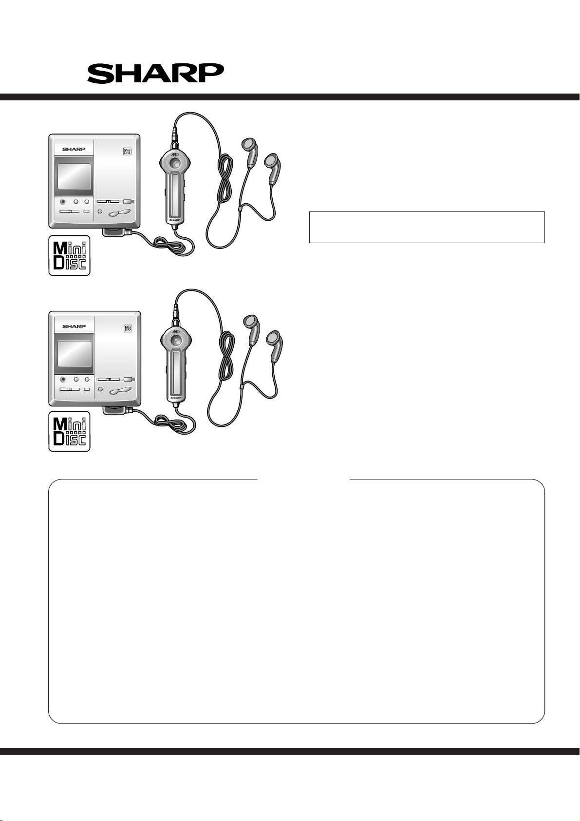
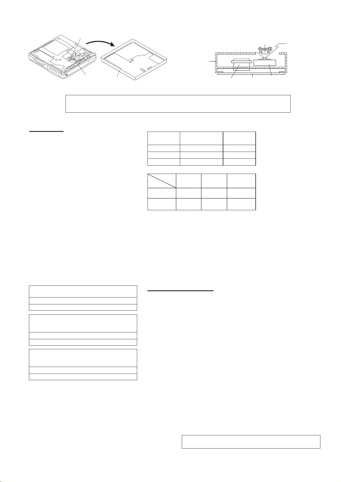
Illustration: MD-MT831H
MD-MT831H/W
SERVICE MANUAL
No. SX963MDMT831H
MD-MT831H(GL)
MD-MT831W(GL)
• In the interests of user-safety the set should be restored to its
original condition and only parts identical to those specified be
used.
Illustration: MD-MT831W
CONTENTS
SAFETY PRECAUTION FOR SERVICE MANUAL ............................................................................................................... 2
SPECIFICATIONS ................................................................................................................................................................. 3
NAMES OF PARTS ............................................................................................................................................................... 4
OPERATION MANUAL.......................................................................................................................................................... 5
QUICK GUIDE ....................................................................................................................................................................... 8
DISASSEMBLY.................................................................................................................................................................... 10
REMOVING AND REINSTALLING THE MAIN PARTS....................................................................................................... 11
ADJUSTMENT ...................................................................................................................................................................... 12
MD ERROR MESSAGE DISPLAY CONTENT LIST ........................................................................................................... 26
BLOCK DIAGRAM ............................................................................................................................................................... 27
SCHEMATIC DIAGRAM ...................................................................................................................................................... 28
VOLTAGE ............................................................................................................................................................................ 31
WIRING SIDE OF P.W.BOARD........................................................................................................................................... 32
WAVEFORMS OF MD CIRCUIT ......................................................................................................................................... 35
NOTES ON SCHEMATIC DIAGRAM .................................................................................................................................. 36
TYPES OF TRANSISTOR AND DIODE .............................................................................................................................. 36
TROUBLE SHOOTING........................................................................................................................................................ 37
FUNCTION TABLE OF IC.................................................................................................................................................... 40
PARTS GUIDE/EXPLODED VIEW
PACKING METHOD (MD-MT831H FOR U.K. ONLY)
Page
SHARP CORPORATION
– 1 –
This document has been published to be used
for after sales service only.
The contents are subject to change without notice.
Page 2
MD-MT831H/W
SAFETY PRECAUTION FOR SERVICE MANUAL
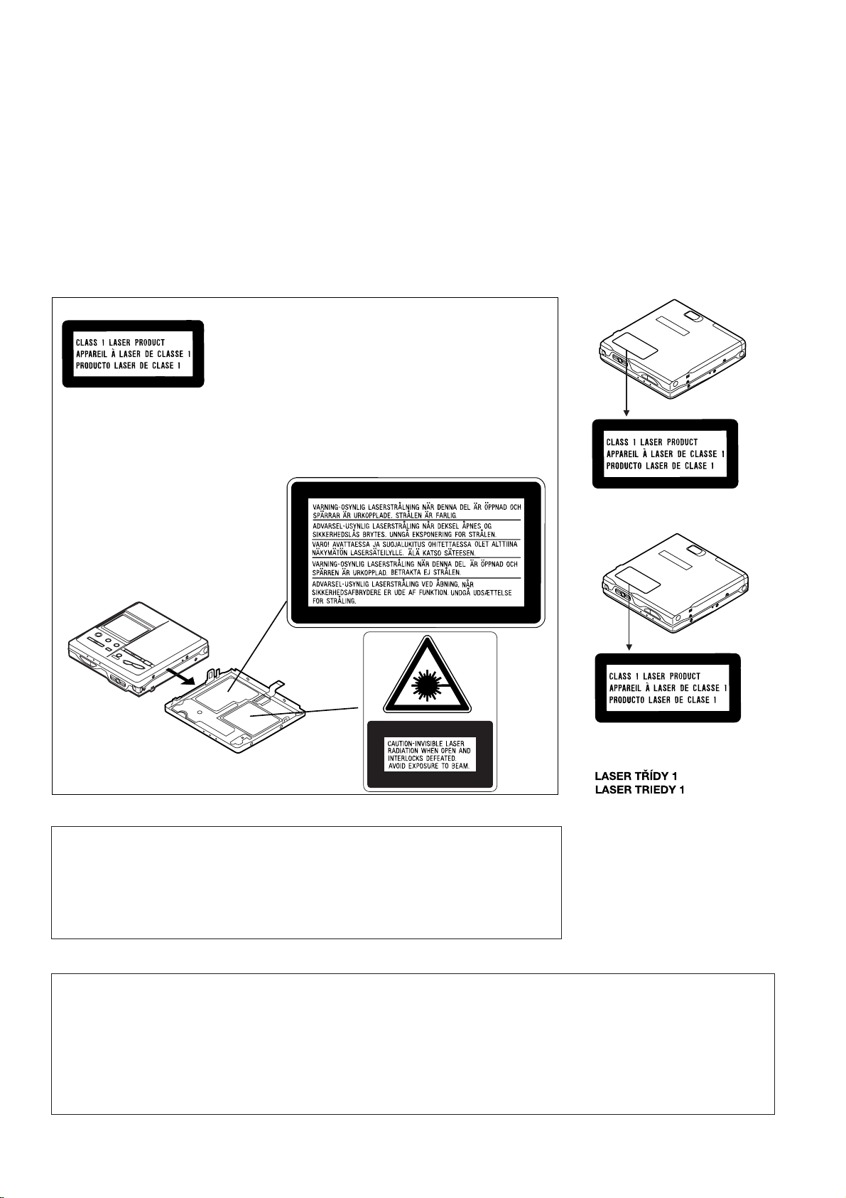
Precaution to be taken when replacing and servicing the Laser Pickup.
The AEL (Accessible Emission Level) of Laser Power Output for this model is specified to be lower than Class I Requirements.
However, the following precautions must be observed during servicing to protect your eyes against exposure to the laser beam.
(1) When the cabinet has been removed, the power is turned on without a compact disc, and the Pickup is on a position
outer than the lead-in position, the Laser will light for several seconds to detect a disc. Do not look into the Pickup Lens.
(2) The Laser Power Output of the Pickup inside the unit and replacement service parts have already been adjusted prior
to shipping.
(3) No adjustment to the Laser Power should be attempted when replacing or servicing the Pickup.
(4) Under no circumstances look directly into the Pickup Lens at any time.
(5) CAUTION - Use of controls or adjustments, or performance of procedures other than those specified herein may result
in hazardous radiation exposure.
CAUTION
● This Portable MiniDisc Recorder is classified as a CLASS 1 LASER product.
● The CLASS 1 LASER PRODUCT label is located on the bottom.
Use the Portable MiniDisc Recorder only in accordance with the instructions given in
●
this manual and do not attempt to interfere with the interlock switch or make any
other adjustment as this may result in exposure to hazardous radiation.
Laser Diode Properties
● Material: GaAIAs
● Wavelength: 785 nm
● Pulse time:
Read mode; 0.8 mW Continuous
Write mode; max. 10 mW 0.5S
min. cycle 1.5S
Repetition
(MD-MD831H for U.K.)
LASER KLASSE 1
LUOKAN 1 LASERLAITE
KLASS 1 LASERAPPARAT
(MD-MD831H for Europe)(For MD-MD831W)
VAROITUS! LAITTEEN KÄYTTÄMINEN MUULLA KUIN TÄSSÄ KÄYTTÖOHJEESSA
MAINITULLA TAVALLA SAATTAA ALTISTAA
KÄYTTÄJÄN TURVALLISUUSLUOKAN 1 YLITTÄVÄLLE
NÄKYMÄTTÖMÄLLE LASERSÄTEILYLLE.
VARNING - OM APPARATEN ANVÄNDS PÅ ANNAT SÄTT ÄN I DENNA BRUKSANVISNING
SPECIFICERAS. KAN ANVÄNDAREN UTSÄTTAS FÖR OSYNLIG LASERSTRÅLNING, SOM
ÖVERSKRIDER GRÄNSEN FÖR LASERKLASS 1.
(MD-MD831H for Europe)
Precaution to be taken when replacing and servicing the laser pickup.
The following precautions must be observed during servicing to protect your eyes against exposure to the laser.
Warning of possible eye damage when repairing:
If the AC adaptor or batteries are connected when the top houising (disc cover) of the unit is removed, and the PLAY key is
pressed, the laser will light up during focus access (2-3 seconds). (Fig. 3-1) During the operation, the laser will leak from the
opening between the magnetic head and the mechanical chassis (Fig. 3-2). In order to protect your eyes, you must not look
at the laser during repair. Before repairing be sure to disconnect the AC adaptor and remove the batteries.
– 2 –
Page 3
g
Magnet head
Magnet Head
Laser Beam
Optical Pickup
Main PWB
Spindle motor
Mechanism
Chassis
MD-MT831H/W
Optical pickup
Top Cabinet
Figure 3-1 Figure 3-2
FOR A COMPLETE DESCRIPTION OF THE OPERATION OF THIS UNIT, PLEASE REFER TO
THE OPERATION MANUAL.
■ General
Power source:
DC 3.6V: Rechargeable Lithium-Ion battery
x 1
DC 5.0V: AC adaptor (AC 220 - 230V, 50/
DC 5.0V: AC adaptor (AC 230 - 240V, 50/
DC 5.0V: AC adaptor (AC 110 - 240V, 50/
DC 3.3V: Battery case (with voltage booster)
DC 4.5V: Separately available car adaptor,
Power consumption:
7 W (AC adaptor) [MD-MT831H]
0.15A (AC adaptor) [MD-MT831W]
Output power:
RMS; 20 mW (10 mW + 10 mW) (0.2% T.H.D.)
Charging time:
Approx. 3 hours
(When using the AC adaptor included with the
unit)
Battery life:
When using the rechargeable battery (fully
charged) included with the unit
Continuous recording:Approx. 9.5 hours
Continuous play:Approx. 14.5 hours
When using one, commercially available, high
capacity, “AA” size, alkaline battery (The rechargeable battery is in the unit, discharged.)
Continuous recording:Approx. 4.5 hours
Continuous play:Approx. 11.5 hours
When using one, commercially available, high
capacity, “AA” size, alkaline battery with the rechargeable battery (fully charged)
Continuous recording:Approx. 14 hours
Continuous play:Approx. 26 hours
● The continuous recording time is for analogue
inputs when the volume level is set to “VOL 0”.
● The continuous play time shows the value
when the volume level is set to “VOL 15”.
● The above values are the standard values
when the unit is charged and used at an ambient temperature of 20°C (68°F).
● The operating time when using an alkaline
battery may be different, depending on the type
and manufacturer of the battery, and on the
operatin
60 Hz) [MD-MT831H for Europe]
60 Hz) [MD-MT831H for U.K.]
60 Hz) [MD-MT831W]
(commercially available, “AA”
size, alkaline battery x 1)
AD-CA20X (for cars with a 12-
24V DC negative earth electrical
system)
temperature.
SPECIFICATIONS
Input sensitivity:
Recording
level
Reference input
level
Input
impedance
MIC H 0.25 mV 10 k ohms
MIC L 2.5 mV 10 k ohms
LINE
100 mV 20 k ohms
Output level:
Earphones
LINE
Specified
output
—
250 mV
(-12dB)
Maximum
output level
10 mW +
10 mW
—
impedance
32 ohms
10 k ohms
Dimensions:
Width: 79.4 mm (3-1/8")
Height:17.9 mm (11/16")
Depth: 81.8 mm (3-3/16")
Weight:
163 g (0.36 lbs.) with rechargeable battery
Input socket:
Line/optical digital, microphone (powered by
the main unit)
Output socket:
Earphones (impedance: 32 ohms)/remote
control unit
■ MiniDisc Recorder
Type:
Portable MiniDisc recorder
Signal readout:
Non-contact, 3-beam semi-conductor laser
pick-up
Audio channels:
Stereo 2 channels/monaural (long-play mode)
1 channel
Frequency response:
20 – 20,000 Hz (± 3 dB)
Rotation speed:
Approx. 400 – 1,350 rpm
Error correction:
ACIRC (Advanced Cross Interleave ReedSolomon Code)
Coding:
ATRAC (Adaptive Transform Acoustic Coding),
24-bit computed type
Recording method:
Magnetic modulation overwrite method
Sampling frequency:
44.1 kHz (32 kHz and 48 kHz signals are converted to 44.1 kHz,
Wow and flutter:
Unmeasurable (less than ±0.001% W. peak)
and then recorded.)
Specifications for this model are subject to change without prior
notice
Load
– 3 –
Page 4
MD-MT831H/W
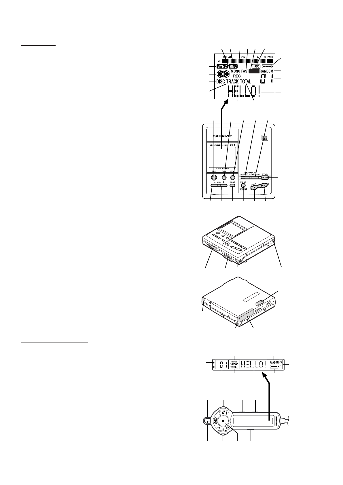
■ Main unit
1. Monaural Long-Play Mode Indicator
2. Record Indicator
3. Level Meter
4. Fast Play Indicator
5. Repeat Indicator
6. TOC Indicator
7. Battery Indicator
8. Random Indicator
9. Track Number Indicator
10. Character/Time Information Indicator
11. Synchro Recording Indicator
12. Disc Mode Indicator
13. Disc Name Indicator
14. Track Name Indicator
15. Remaining Recording Time Indicator
16. Total Track Number Indicator
17. Record/Track Mark Button
18. Display/Character Select Button
19. Edit/Auto Mark/Time Mark Button
20. Fast Reverse/Recording Level Down/
Name Select Button
21. Fast Forward/Recording Level Up/
Name Select Button
22. Enter/Fast Play/Synchro Button
23. Volume Down/Cursor Button
24. Volume Up/Cursor Button
25. Bass/Fade Time/Delete Button
26. Mode/Fade Button
27. Stop/Power Off Button
28. Play/Pause Button
NAMES OF PARTS
123456
11
12
13
14
15 16
172718 20 21
19
26252423
7
8
9
10
22
28
29. Open Lever
30. Remote Control/Earphones Socket
31. Handstrap Holder
32. Optical/Line Input Socket
33. Hold Switch
34. 5V DC Input Socket
35. Microphone Input Socket
36. Battery Cover
■ Remote control unit
1. Disc Mode Indicator
2. Random Indicator
3. Record Indicator
4. Synchro Recording Indicator
5. Track Number Indicator
6. Total Track Number Indicator
7. Character/Time Information Indicator
8. Battery Indicator
9. Repeat Indicator
10. Attachment Eye
11. Play/Pause/Fast Reverse/
Fast Forward Shuttle Switch
12. Play Mode Button
13. Sound/Track Mark Button
14. Earphones Socket
15. Display/Volume Shuttle Switch
16. Stop/Power Off Button
17. Hold Switch
29
30 31 32
34
35 36
12
3
4
6587
1110 12 13
1514 1716
33
9
– 4 –
Page 5
OPERA TION MANUAL
Caution:
● Whilst you are using the rechargeable
battery and the alkaline battery at the
same time, do not remove either of them.
If you do, when the unit is in the play
mode, playback will stop. When in the
recording mode, the recorded contents
will be erased, and the power may be
disconnected.
● Do not use rechargeable batteries
(nickel-cadmium battery etc.) in the bat-
tery case.
● If the unit is not used for a long period of
time, remove the battery. (Even if the
power is turned off, the battery will drain
slowly but continuously.)
● Remove the battery if it is weak or if the
unit is not in use for long periods to pre-
vent potential damage due to battery
leakage.
● Be sure to hold the plug when removing
it. If you pull on the lead, it may break,
or the unit may malfunction.
● Do not use any car adaptor except for
the separately available AD-CA20X.
● For information about the battery life, see
the battery item in the SPECIFICA-
TIONS.
● This unit should only be used within the
range of 0°C (32°F) and 40°C (104°F).
■ Alkaline battery power with a
rechargeable battery
If you use the battery case and the re-
chargeable battery at the same time, the
MD can play much longer than with only
one source of battery power.
● Use one commercially available alkaline
battery (LR6, “AA” size).
1
Make sure that a rechargeable battery
is inserted.
● The external battery case should not
be used unless the rechargeable
battery is installed in the main unit.
2
Insert the battery into the battery case.
(1) Open the case cover.
(2) Insert the battery according to the
polarity marked on the inside of the
battery case. Then, close the case
cover.
3
Attach the battery case to the main unit.
(1) Match the bumps on the battery case
to the holes in the main unit.
(2) Turn the screw in the direction
marked “LOCK” to secure the bat-
tery case.
■ AC power
1
Connect the lead from the AC adaptor
to the DC IN 5V socket on the main unit.
2
Plug the AC adaptor into an AC socket.
Notes:
● When there is thunder or lightning in your
vicinity, unplug the AC adaptor from the
AC socket.
● When power failure occurs whilst play-
ing back using the AC adaptor, discon-
nect the adaptor from the outlet. Other-
wise, playback may start automatically
when the power returns.
● When the unit is not in use for extended
periods, remove the AC adaptor from the
AC socket.
● Never use an AC adaptor other than the
one specified. Otherwise, problems or
serious hazards may be created.
● Do not bend, twist or tie the power lead
or put heavy objects on top of it.
2
3
1
2
RELEASE LOCK
Press.
Open.
Back of the
MD recorder
4
1
2
3
1
2
3
POWER SOURCE
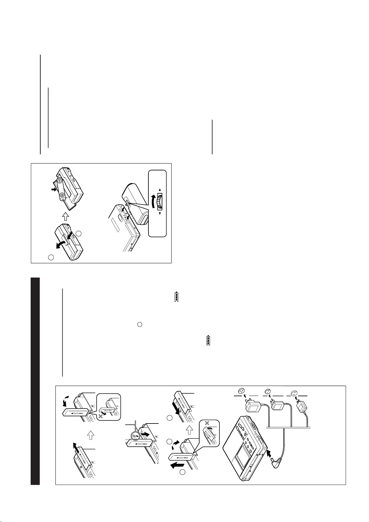
■ Rechargeable battery power
This unit can be used with the following power sources: a rechargeable battery, an AC
adaptor, a battery case, and a separately available car adaptor (AD-CA20X).
When the rechargeable battery is used for
the first time or when you want to use it af-
ter a long period of disuse, be sure to charge
it fully.
1
Open the battery cover.2Insert the rechargeable battery.
● Insert the side with the arrow first.
3
Close the battery cover.
● Do not fold down the cover before
pulling it up as 1
shows. The cover
may break.
4
Plug the AC adaptor into the AC socket,
and then insert the plug on the AC adap-
tor lead into the DC IN 5V socket.
● About 4 seconds later, “
” will
flash, and the battery will begin charg-
ing.
● Battery charging will be complete in
3.0 hours. When the charging is com-
plete, “ ” will go out.
Mark
To the DC IN 5V socket
Insert securely
,
all the way in.
Caution:
● Do not remove the plastic around the
rechargeable battery. Heat generation,
fire and explosion can result.
Notes:
● After charging has been completed, the
AC adaptor may be left connected.
(For example, when charging at night)
● If the rechargeable battery is in the unit,
it will be charged, even whilst operating
the unit. (Float charge)
● Do not force the battery cover open too
far.
● When the AC adaptor plug is inserted
and a MiniDisc has already been in-
serted, playback may start automatically.
In this case, press the
•
■/:OFF button
twice to turn the power off.
AC 110V-240V, 50/60 Hz
(For MD-MT831W)
AC 230V-240V, 50/60 Hz
(MD-MT831H for U.K.)
AC 220V-230V, 50/60 Hz
(MD-MT831H for Europe)
MD-MT831H/W
– 5 –
Page 6

MD-MT831H/W
Many potential “problems” can be resolved by the owner without calling a service technician.
If something seems to be wrong with this product, check the following before calling your
authorised SHARP dealer or service centre.
■ If trouble occurs
When this product is subjected to strong
external interference (mechanical shock,
excessive static electricity, abnormal sup-
ply voltage due to lightning, etc.) or if it is
operated incorrectly, it may malfunction.
If such a problem occurs, do the following:
1. Unplug the AC adaptor from the AC
socket.
2. Remove the battery.
If trouble occurs with a particular MiniDisc
● Depending on the MiniDisc, sound may skip or stop during playback if there is some-
thing wrong with the stored information. In such a case, try another MiniDisc before
calling for service.
3. Leave the unit completely unpowered for
approximately 30 seconds.
4. Plug the AC adaptor back into the AC
socket and retry the operation.
If strange sounds, smell or smoke come out
of the unit or an object is dropped into the
unit, remove the AC adaptor from the AC
socket immediately and contact an
authorised SHARP service centre.
PROBLEM CAUSE
The unit does not turn
on.
● Is the AC adaptor disconnected?
● Is the battery exhausted?
● Is the unit in the hold mode?
● Has condensation formed inside the unit?
● Is the unit being influenced by mechanical shock or by
static electricity?
● Is the volume set too low?
● Is the remote control unit or the earphones plugged in?
● Are you trying to play a MiniDisc with data on it instead
of a MiniDisc containing music?
● Is the unit in the hold mode?
● Is the battery exhausted?
● Is the remote control unit plug or the earphone plug in-
serted firmly?
● Is the battery exhausted?
● Is the unit being subjected to excessive vibration?
● Has the track number or character information been
written on the disc yet?
● Is the unit in the recording or editing mode?
● Is the MiniDisc protected against accidental erasure?
● Is the unit connected properly to the other equipment?
● Is the AC adaptor unplugged or did a power failure oc-
cur whilst recording or editing?
● Is the unit in the hold mode?
● Is an optical signal being output from the external equip-
ment?
Read the operation manual for the external equipment.
No sound is heard from
the earphones.
When the operation
buttons are pressed, the
unit does not respond.
Some sounds are
skipped.
The MiniDisc cannot be
ejected.
Recording and editing
are impossible.
TROUBLESHOOTING
■ Moisture condensation
In the following cases, condensation
may form inside the unit.
● Shortly after turning on a heater.
● When the unit is placed in a room where
there is excessive steam or moisture.
● When the unit is moved from a cool
place to a warm place.
When the unit has condensation inside,
the disc signals cannot be read, and the
unit may not function properly.
● If this happens, remove the disc.
The condensation should evaporate in
approximately 1 hour. The unit will then
function properly.
When the number of tracks used reaches
the limit, regardless of the remaining re-
cording time, further recording will be
impossible.
(Maximum number of tracks: 255)
If a MiniDisc has been recorded or ed-
ited repeatedly or if a MiniDisc has
scratches on it, it may not be possible to
record the maximum number of tracks on
it.
If there are scratches on a disc, the unit
will automatically avoid recording in those
areas. The recording time will be reduced.
When the remaining recording time of a
disc is displayed, short tracks less than
12 seconds long may not be included in
the total.
For MiniDiscs on which repeated record-
ing and editing operations were per-
formed, the COMBINE function may not
work.
A cluster (about 2 seconds) is normally the
minimum unit of recording. So, even if a track
is less than 2 seconds long, it will use about
2 seconds of space on the disc.
Therefore, the time actually available for re-
cording may be less than the remaining time
displayed.
If there are scratches on discs, those sec-
tions will be automatically avoided (no record-
ing will be placed in those sections). There-
fore, the recording time will be reduced.
For MiniDiscs on which repeated record-
ing and editing were performed, some
sounds may be skipped whilst cueing and
reviewing.
If there are scratches or dust on a
MiniDisc, the track numbers following that
track will be increased by one.
MINIDISC SYSTEM LIMITATIONS
MiniDiscs are recorded using a different system than is used for cassette tapes or DAT
recordings. Therefore, the following conditions may be encountered, depending on how
the disc has been recorded or edited. These are due to system limitations, and should be
considered normal.
Even if the maximum recording
time of a MiniDisc has not been
reached, “DISC FULL” or “TOC
FULL” may be displayed.
Even if the number of tracks and
the recording time have not
reached the limit, “DISC FULL”
may be displayed.
Even if several short tracks are
erased, the remaining recording
time may not show an increase.
Two tracks may not be combined
in editing.
The total of the recorded time and
time remaining on a disc may not
add up to the maximum possible
recording time.
When recorded tracks are played
back using the cue and review op-
erations, some sounds may be
skipped.
A track number can be created in
the middle of a track.
– 6 –
Page 7
MD-MT831H/W
ERROR MESSAGES
PLAY MD
(PLAY md)
● You tried to record on a playback-
only disc.
● Replace it with a recordable disc.
Error messages RemedyMeaning
BLANK MD
(BLANK)
BATT EMPTY
(Lo BATT)
● The battery is run down. ● Charge the rechargeable battery or
replace the alkaline battery (or use
the AC adaptor for power).
● Nothing is recorded. ● Replace the disc with a recorded disc.
Can’t FADE
Can’t A.F
● The recordable time is shorter than
the fading time
● Record after you check the remain-
ing recording time.
Can’t COPY
(Can’t C)
● No copy can be made because of
the SCMS copyright system.
● Record using the analogue cable.
Can’t EDIT
(Can’t E)
● A track cannot be edited. ● Change the stop position of the track
and then try editing it.
Can’t READ*
(Can’tS)
(Can’T)
(Can’tU)
● The disc is damaged. ● Reload the disc or replace it.
● Replace it with another recorded disc.
Can’t REC
(Can’t R)
●
Recording cannot be performed cor-
rectly due to vibration or shock in the unit.
● Re-record or replace it with another
recordable disc.
Can’t STAMP
● Editing is impossible. ● Check the number of tracks.
Can’t WRITE
(can’tW)
● Cannot save the TOC information
correctly to a MiniDisc.(A large por-
tion of the disc has been damaged.)
● Replace the disc with another re-
cordable disc.
DEFECT
(DEFECT)
● The disc is scratched. ● If the sound you hear is not right, try
recording again.
● Replace the disc with another re-
cordable disc.
DISC FULL
● The disc is out of recording space. ● Replace it with another recordable
disc.
HOLD
(HOLD)
LOCKED
(Can’t LOCK)
NO DISC
Er-MD**
(ErMD*)
NO SIGNAL
(noSIG.)
● Poor connection of the digital cable.
● No output signal comes out from the
external unit to playback.
● The unit is in the hold mode. ● Return the HOLD switch to its origi-
nal position.
● The OPEN lever was moved during
recording or editing.
● Turn off the power and remove the
MiniDisc.
● A disc has not been loaded. ● Load a disc.
● You have come to the conclusion
that the unit is out of order.
● T o have it repaired, go to the distribu-
tor where you purchased the unit.
● Connect the digital cable securely.
● If the portable CD player has a function
to prevent sound skips,deactivate it.
● Playback with the connected unit.
( ) : Error messages seen on the remote control.
* : Number or Symbol.
TEMP OVER
(TEMP!)
TOC FULL
Tr. Protect
? DISC
(? DISC)
● The temperature is too high. ● Turn off the power, and wait for a
while.
● There is no space left for recording
character information (track names,
disc names, etc.).
● Replace it with another recordable
disc.
● A disc which contains data other than
music was played.
● There is an error in the signal from
the disc.
● A disc which contains non-music
data cannot be played.
● Replace it with another recorded
disc.
● The track has been protected from
being erased.
● Edit the track with the device on
which it was recorded.
SORRY
(SORRY)
● Since a track number is currently
being located or written to, the unit
cannot accept your command.
● Wait for a while and try the opera-
tion again.
PROTECTED
● The MD is write protected.
● You tried to record without loading
an MD
● A playback-only MD was loaded
and the REC button was pressed
when the power was off.
● Move the write protection knob back
to its original position.
● Load a recordable MD.
● Replace it with a recordable MD.
Error messages RemedyMeaning
POWER ?
● Improper power is being supplied. ● Use one of the specified power
sources.
TOC FORM**
(T form**)
● There is an error in the recording sig-
nal
● Erase all of the signal errors, and
then try recording again.
( ) : Error messages seen on the remote control.
* : Number or Symbol.
CONVENIENT OPERATION OF THE UNIT
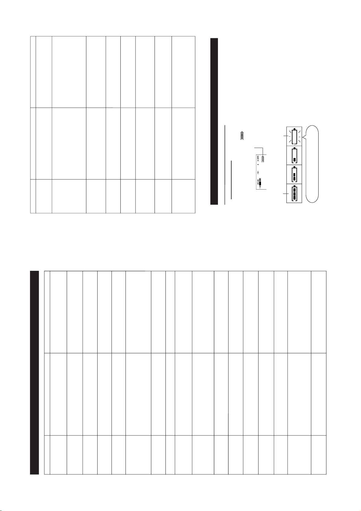
■ Checking the remaining amount
of battery charge
The remaining amount of battery charge
is shown by the battery indicator (
)
during operation.
< How to read the battery indicator >
● When the battery is completely discharged,
the whole battery indicator will flash. Re-
charge the battery or replace the alkaline
battery with a new one.
● When the battery has run completely out,
“BATT EMPTY” (main unit) and “Lo BA TT”
(remote control unit) will appear. Then, the
power will be disconnected automatically.
Notes:
● When using the unit with an alkaline bat-
tery or a rechargeable battery, the battery
indicator will not correctly display the remain-
ing capacity for approximately 20 seconds
after the power has been turned on.
● When the AC adaptor included with this unit
or a separately available car adaptor is
used, the battery indicator will not be shown.
● The number of bars shown in the battery
indicator may increase or decrease, de-
pending on the operation being performed.
This is normal.
● When the rechargeable battery and the al-
kaline battery are used at the same time,
the rechargeable battery is used first, then
the alkaline battery.
Since the battery indicator shows the re-
maining amount of the particular battery
being used, the number of bars will in-
crease when the unit switches to the al-
kaline battery.
Battery indicator
When the battery needs charging, it is
impossible to start recording or editing.
When the battery is
completely charged
Charging is
needed.
– 7 –
Page 8
MD-MT831H/W
3
Insert a MiniDisc.
PLA YING A MINIDISC
1
Insert the earphones plug firmly into the earphones socket
on the remote control unit.
2
Plug the remote control unit into the socket on the main
unit. Push the plug all the way in.
4
■ Play
■ Adjust the Volume
To interrupt playback:
Press the button.
● T o resume playback, press the button again.
To stop playback:
Press the
•
■/:OFF button.
To turn off the power:
Press the
•
■/:OFF button whilst in the stop mode.
Volume (0 - 30)
■ Adjust the bass level
BASS 1
BASS 2
BASS 3
BASS OFF
Bass sounds are emphasised slightly
Bass sounds are emphasised more.
Bass sounds are emphasised even
more.
Bass emphasis is cancelled.
SOUND CONTROL
● Playback starts automatically with a
play-back only MiniDisc or a MiniDisc
which is protected against acciden-
tal erasure. (Auto-play function)
■ Insert a MiniDisc
LOADING/UNLOADING A MINIDISC
■ Remove the MiniDisc
■ Remote Control Unit/Earphones
CONNECTION
2
1
3
4
2
1
3
DIGITAL OUT
RL
AUDIO OUT
■ Analog recording
■ Digital recording
■ Microphone
RIGHT LEFT
Analogue cable included with this unit
Optical digital cable included with this unit
MIC IN
OPEN
OPEN
REMOTE
OPTICAL
/
LINE IN
OPTICAL
/
LINE IN
QUICK GUIDE
– 8 –
Page 9
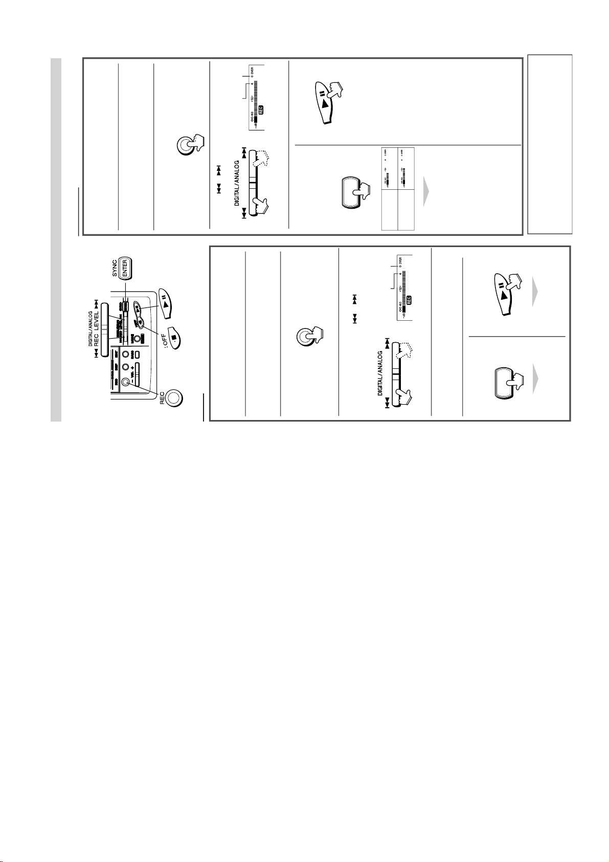
MD-MT831H/W
RECORDING
1
Connect the external equipment.
2
Insert a recordable MiniDisc.
3
REC
REC LEVEL
■ Audio
<Synchro Recording>
6
<Manual Recording>
ENTER
SYNC
■ Microphone
ENTER
SYNC
1
Connect the stereo microphone to the MIC IN socket.
2
Insert a recordable MiniDisc.
3
REC
To stop recording:
Press the
•
■/:OFF button.
To turn off the power:
Press the
•
■/:OFF button whilst in the stop mode.
<Synchro Recording>
5
<Manual Recording>
5
Put the equipment connected to this unit into the playback
stand-by mode.
Begin playback on the
source equipment.
MIC SYNC H
MIC SYNC L
–24dB
–12dB
When a sound, such as a per-
son speaking, is picked up by
the microphone, recording will
begin automatically
.
● If a silence lasts for 3 sec-
onds or more, the record-
ing will be paused auto-
matically. However , the unit
will not pause for about the
first 10 seconds after re-
cording has started.
4
Whilst playing sound from the external equipment con-
nected to this unit, press the or button to adjust
the recording level.
0dB–4dB
Start playback on the
equipment connected
to this unit.
4
Press the or button to adjust the recording level.
0dB–4dB
Press the ENTER/SYNC but-
ton to select the synchro re-
cording level.
REC LEVEL
– 9 –
Page 10
MD-MT831H/W
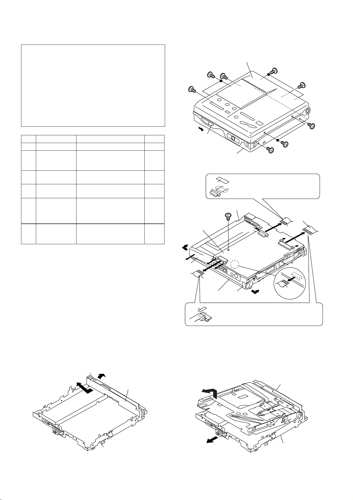
DISASSEMBLY
Cares before disassembling
When assembling the machine after disassembling or
repair, observe the following requirements so as to
ensure safety and performance.
1. Remove the batteries from the machine, and take out the
mini-disc.
2. When assembling after repair, be sure to restore the
initial location of wires.
Since the screws are small, incorrect fixing may result in
malfunction.
3. When repairing, pay utmost attention to static electricity
of IC.
(B1)x2
ø1.4x2mm
(A1)x1
ø1.4x2mm
Top Cabinet
(A1)x1
ø1.4x2mm
(B1)x2
ø1.4x2mm
(A1)x1
ø1.4x2mm
STEP
REMOVAL
1 Bottom Cabinet 1. Screw ..................... (A1) x5 10-1
2 Top Cabinet 1. Open the Top Cabinet 10-1
3 Center Cabinet A 1. Open the Battery Cover 10-2
4 Main PWB 1. Screw .................... (C1) x1 10-2
5 Mechanism Unit
6 Jack PWB
PROCEDURE
2. Screw ..................... (B1) x6
3. Flexible PWB.......... (B2) x1 10-2
2.
Remove in the arrow direction.
2. Flexible PWB......... (C2) x3
1.
Slacken the main frame in 10-3
the direction of A, then
remove it in the direction
of B.
1.
Lift the metal fitting in the 10-4
direction of C and remove
it in the direction of D.
FIGURE
Battery
Cover
Open Lever
Bottom Cabinet
(C1)x1
ø1.7x2.5mm
Main PWB
Pull
Pull
(B2)x1
Center
Cabinet B
Felt
(A1)x1
ø1.4x2mm
(A1)x1
ø1.4x2mm
(B1)x2
ø1.4x2mm
Figu re 10-1
Felt
When assembling, attach felt to the
flexible PWB not to the connector.
If it is slack, it may touch the sheet metal.
Main Frame
Pull
Center
Cabinet A
When assembling, put the folded flexible PWB on
the connector and attach felt to it. If it is slack,
it may touch the sheet metal.
(C2)x1*
Flexible PWB
for optical
pickup
(C2)x1
Pull
Pull
(C2)x1
Bracket
D
Figure 10-4
C
Main Frame
Jack PWB
Caution:
Carefully handle the main PWB and flexible PWB. After removing the
flexible PWB (*1) for the optical pickup from the connector, do not
touch directly the front end of flexible PWB with your hand so as to
prevent damage of optical pickup by static electricity.
Figure 10-2
Mechanism Unit
B
A
Main Frame
Figure 10-3
– 10 –
Page 11
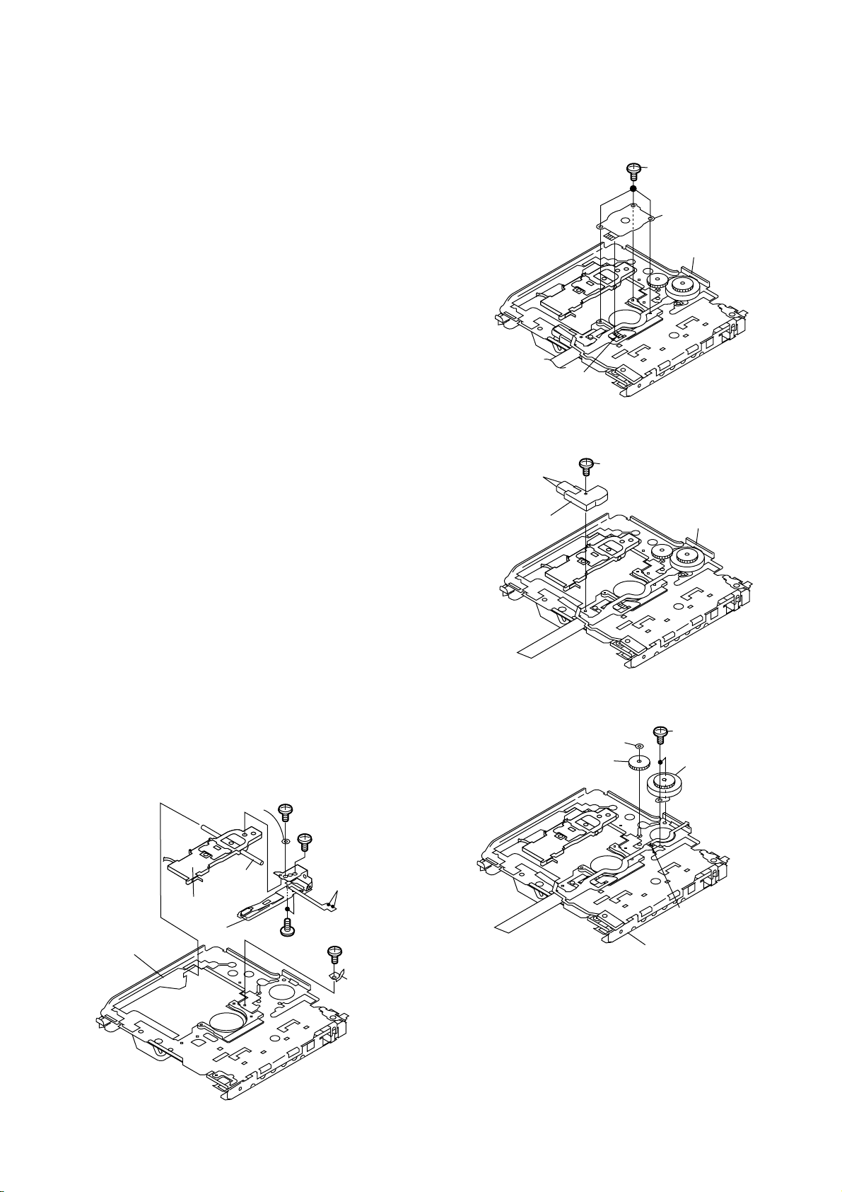
REMOVING AND REINSTALLING THE MAIN PARTS
Remove the mechanism according to the disassembling methods 1 to 5. (See Page 10.)
MD-MT831H/W
How to remove the spindle motor (See Fig. 11-1.)
1. Remove the solder joint (A1) x 4 of flexible PWB.
2. Remove the screws (A2) x 3 pcs., and remove the spindle
motor.
How to remove the lift motor (See Fig. 11-2.)
1. Remove the solder joint (B1) x 2 of Lift motor.
2. Remove the screw (B2) x 1 pc., and remove the lift motor.
Note:
Take care so that the motor gear is not damaged.
(If the gear is damaged, noise is caused.)
How to remove the sled motor (See Fig. 11-3.)
1. Remove the stop washer (C1) x 1 pc., and remove the drive
gear (C2) x 1 pc.
2. Remove the screws (C3) x 2 pcs.
3. Remove the solder joints (C4) x 2 of flexible PWB and
remove the sled motor.
Note:
Take care so that the motor gear is not damaged.
(If the gear is damaged, noise is caused.)
How to remove the magnetic head (See Fig. 11-4.)
1. Remove the screws (D1) x4 which connects the magnetic
head to the head relay flexible PWB, remove the spring
washers (D2) x 1 and remove the soldering joints (D3) x 2.
Note:
Mount carefully so as not to damage the magnetic head.
(If the gear is damaged, noise is caused.)
Mechanism Flexible
PWB Solder Joint
(A1)x4
Solder Joint
(B1)x2
Lift Motor
(A2)x3
ø1.4x2.8mm
Spindle Motor
MD Mechanism
Figure 11-1
(B2)x1
ø1.4x4.5mm
MD Mechanism
How to reinstall the optical pickup unit
(See Fig. 11-4.)
1. Remove the screw (E1) x 1 pc.
2. Slowly raise the optical pickup.
(D2)x1
Shaft
Pickup Unit
Magnetic head
MD Mechanism
(D1)x1
ø1.4x2.2mm
(D1)x1
ø1.4x1.8mm
Solder Joint
(D3)x2
(D1)x2
ø1.4x1.1mm
(E1)x1
ø1.7x3mm
Spring
Figure 11-2
(C1)x1
(C2)x1
Figure 11-3
(C3)x2
ø1.4x1.2mm
Sled Motor
Solder Joint
(C4)x2
MD Mechanism
Figure 11-4
– 11 –
Page 12
MD-MT831H/W
Test disc
ADJUSTMENT
MD adjustment needs two types of disc, namely recording disc (low reflection disc) and playback-only disc (high
reflection disc).
Type
1 High reflection disc MMD-110 (TEAC Test MD) 88GMMD-110
2 Low reflection disc MMD-213A (TEAC Test MD) 88GMMD-213A
3 Low reflection disc Recording minidisc UDSKM0001AFZZ
Test disc Parts No.
Note: Use the low reflection disc on which music has been recorded.
Entering the TEST mode
1. Setting at port (in standby state, disc-free state or power nonconnected state)
(1) Set the port as follows.
TEST1 : "Low"
TEST0 : "High"
(2) Press the PLAY button in the standby state (it is allowed to insert the disc or to connect the power supply).
(3) Test Mode STOP [ T E S T _ ]
2. Setting by special button operation (in standby state)
Test mode: Perform it with the remote control.
(1) Press and hold the "PLAY MODE" button on the remote control and press the "PLAY" button.
(2) Release only the "PLAY MODE" button.
(3) Press and hold only the "PLAY" button and press the "VOL-" button.
(4) When the EL on the remote control turns on, release the "VOL-" button
*Since the unit is changed to the setting for production line inspection , be sure to set it to the default setting state in the following default
setting procedure before returning it to the user.
(5) Normal mode setting initialization (BASS setting, VOL setting, etc.)
(6) Indication of microcomputer version for one second [ X X X X X X ]
Destination
Microcomputer version
(7) Whole LCD lighting for 2 seconds
(8) Test Mode STOP [ T E S T _ ]
*When the PLAY button is pressed during indication (6) and (7), the process proceeds to (8).
EEPROM version
Leaving the TEST mode
(1) Press the STOP button in the TEST mode stop state or version indicating state or whole LCD lighting state.
(2) EEPROM rewrite-enable area updating, adjustment error setting .
(3) Change to standby state
Shipping setting method
Press and hold the "VOLUME-DOWN" and "PLAY" buttons on the main unit at the same time, supply power from the DC IN plug [INIT], then
stop the power supply from the DC IN plug after the "BYE OK" display disappears.
Test Mode
1. AUTO 1 Mode • Perform preliminary automatic adjustment.
2. AUTO 2 Mode
3. TEST-PLAY Mode
4. TEST-REC Mode
5. MANUAL 1 Mode
• If the combination of mechanism and pickup
PWB has been changed, be sure to start from
AUTO1.
• Perform ATT (attenuator) automatic adjustment.
• Perform continuous playback (error rate display,
jump test)
• Continuous playback from the specified address
is performed.
• 1 line, 10 lines or 384 lines manual jump is
performed.
• C1 error rate display (pit section), ADIP error
rate display (groove section)
• The temperature correction is performed only when
servo start is performed, but the posture correction
is not performed during continuous playback.
• Continuous record from the specified address
is performed.
• Change of record laser output(servo gain is also
changed according to laser output).
• The temperature correction is performed only
when servo start is performed, but the posture
correction is not performed during continuous
recording.
• Temperature is displayed. (Updating in real time)
• Seeing the displayed adjustment value, perform
preliminary manual adjustment.
(Error rate indication, jump test
6. MANUAL 2 Mode
7. ERROR INFORMATION
Mode • Error information is initialized
8. NORMAL Mode
9. EEPROM Mode
10. INNER Mode
• Temperature is displayed. (Updating in real time)
• Seeing the displayed adjustment value perform
manfully the preliminary adjustment.
(Error rate indication, jump test)
• Continuous playback is performed
(error rate display, jump test).
• Error information is displayed.
• The mode is changed from the TEST mode to
the normal mode without adjustment.
• In the normal mode the internal operation mode,
memory capacity, etc. areindicated.
• In the normal mode both temperature correction
and posture correction are perfomed.
• Factors of digital servo are changed manually.
(Each servo is turned on individually.)
• Cut-off frequency of BASS1, BASS2 and BASS3
is selected manually.
• Temperature detection terminal voltage is
measured, and the reference value is set.
• Defaults are selected and set.
• Setting of EEPROM protect area is updated.
(In case of protect releasing)
• Determine the position where the INNER switch
is turned on. (only high reflection disc).
• The temperature correction is performed only
when servo start is performed, but the posture
correction is not performed.
– 12 –
Page 13

MD-MT831H/W
Operation in each TEST mode
1. AUTO1 Mode
• When the STOP button is pressed while the AUTO1 menu appears or during automatic adjustment, the mode changes to the TEST mode
stop state. At this time the adjustment value is not output.
• Be sure to adjust, using the specified disc MMD-212.
At this time release the EEPROM (IC402) protection. (Refer to EEPROM write procedure.)
• Adjustment NG; Adjustment item out of range, focus ON failure, and adjustment error
• When the PLAY button is pressed while ADJ. OK is displayed, AUTO2 is executed.
2. AUTO2 Mode
• When the STOP button is pressed while the AUTO2 menu appears or during automatic adjustment, the mode changes to the TEST mode
stop state. At this time the adjustment value is not output.
• Adjustment NG; Adjustment item out of range, and adjustment error.
• When the PLAY button is pressed while ADJ. OK is displayed,TEST_PLAY is executed.
3. MANUAL1 Mode
• Adjustment item to be made in AUTO1 mode is performed manually.
• When the VOL UP button is pressed during adjustment, the setting increases, and the new setting is output.
• If the VOL DOWN button is pressed during adjustment, the setting decreases and the new setting is output.
• If the VOL UP/DOWN button is held down, the setting changes continuously with 100 ms cycle.
*In this operation, the setting change is performed for each digit. The digit is changed by pressing the MODE button.
• If the setting is within the allowable range, the RANDOM display lights.
• When the STOP button is pressed during MANUAL1 MENU or measurement or adjustment, the state is changed to the TEST mode stop
state.
4. MANUAL2 Mode
• Adjustment item to be made in AUTO2 mode is performed manually.
• When the VOL UP button is pressed during adjustment, the setting increases, and the new setting is output.
• If the VOL DOWN button is pressed during adjustment, the setting decreases and the new setting is output.
• If the VOL UP/DOWN button is held down, the setting changes continuously with 100 ms cycle.
*In this operation, the setting change is performed for each digit. The digit is changed by pressing the MODE button.
• If the setting is within the allowable range, the RANDOM display lights.
• When the STOP button is pressed during MANUAL2 MENU or measurement or adjustment, the state is changed to the TEST mode stop
state.
• When the PLAY button is pressed in B-ATT set state, the mode is changed to the continuous playback mode.
• As for operation during continuous playback refer to "TEST-PLAY mode explanation".
5. TEST-PLAY Mode
• When the STOP button is pressed while the TEST-PLAY menu appears, or in TEST-PLAY or continuous playback mode, the mode
changes to the TEST mode stop state.
• When the PLAY button is pressed while the TEST-PLAY menu appears,continuous playback is initiated from the current pickup position.
• Whenever the DISP button is pressed in the TEST-PLAY menu, the target address changes as follows.
When the PLAY button is pressed while a target address is displayed, continuous playback is performed after searching that address.
• Each time the MODE button is pressed while the TEST-PLAY mode target address is displayed, the digit which is changed by pressing the
SKIP UP/DOWN button is changed as follows.
• When the SKIP UP button is pressed in the TEST-PLAY mode target address is displayed, the digit of address specified by the MODE
button is set to +1h. (0 to F)
• When the SKIP DOWN button is pressed in the TEST-PLAY mode target address is displayed, the digit of address specified by the MODE
button is set to -1h. (0 to F)
* When the SKIP UP/DOWN button is held down, the setting changes continuously, one cycle being 100 ms.
• When the BASS button is pressed in the continuous playback mode, the number of jump lines changes as follows.
* After the number of jump lines is indicated for one second, the address indication is restored. [ T R _ ]
• When the SKIP UP button is pressed in the continuous playback mode, the specified number of lines is jumped in the FWD direction.
• When the SKIP DOWN button is pressed in the continuous playback mode, the specified number of lines is jumped in the REV direction.
* When the SKIP UP/DOWN button is held down, jump is repeated every approx. 100 ms.
•Whenever the DISP button is pressed in the continuous playback mode, the indication changes as follows.
* Pre-mastered disc
* Recordabl disk
0032 — 03C0 — 0700 — 08A0 — 0950— 0032 —
003
2 — 0032 — 0032 — 0032 —
1 — 10 — 384 — 1
Continuous playback (SUBQ address indication) [ S Q ]
Continuous playback (C1 error indication) [ C E ]
Continuous playback (SUBQ address indication) [ S Q ]
Continuous playback (ADIP address indication) [ A P ]
Continuous playback (C1 error indication) [ C E ]
Continuous playback (ADIP error indication) [ A E ]
Continuous playback (ADIP address indication) [ A P ]
|
|
|
|
|
– 13 –
Page 14

MD-MT831H/W
6. TEST-REC Mode
• When the STOP button is pressed while the TEST-REC menu appears, or in the TEST-REC mode or continuous record mode, the mode
changes to the TEST mode stop state.
• When the PLAY button is pressed while the TEST-REC menu appears, the continuous record is initiated from the current pickup position.
• Whenever the DISP button is pressed in the TEST-REC menu, the target address changes as follows.
0032 — 03C0 — 0700 — 08A0 —0950 — 0032 —
When the PLAY button is pressed while a target address is displayed, continuous playback is performed after searching that address.
• Whenever the MODE button is pressed in the TEST-REC mode target address is displayed, the digit which is changed by the SKIP UP/
DOWN button changes as follows.
0032 — 0032 — 0032 — 0032 —
• When the SKIP UP button s pressed in the TEST-REC mode target address is displayed, the digit of address specified by the BASS button
is set to +1h.(0 to F)
• When the SKIP DOWN button is pressed in the TEST-REC mode target address is displayed, the digit of address specified by the BASS
button is set to -1h. (0 to F)
* When the SKIP UP/DOWN button is held down, the setting changes continuously, one cycle being 100 ms.
• When the VOL UP/DOWN button is pressed in the TEST-REC mode or continuous record mode, the laser record power changes.
(Servo gain changes also according to record power.)
* After the laser record power is indicated for one second, the address indication is restored.
• : Address
• : Laser power cord
• Operation is disabled if the premastered disc or disc is in miserase-protected state.
7. NORMAL Mode
• When the STOP button is pressed while the NORMAL menu appears, the mode changes to the TEST mode stop state.
• Indication during operation
Indication of memory capacity on main unit LCD [ ] + Level meter
: Internal mode
: Address (Cluster section)
: Address (Sector section)
• Selection of sound volume, BASS, etc. is possible (without indication)
• Recording is also possible.
• If the STOP button is pressed during operation in the NORMAL mode, the NORMAL mode is canceled, and the power is turned off.
[ R P W _ ]
8. Error data display Mode
• Reversing when SKIP DOWN button is pressed
• When the STOP button is pressed while the error data indication menu appears or during error data indication, the mode changes to the
TEST mode stop state.
• Error data 0 is the latest error.
• Error which occurred in the TEST mode is also stored in the memory.
• When the DISP button is pressed while the error data indication menu appears, the error data is initialized. [ C L E A R _ ]
: Error Code
•
Explanation of error history code
13h : Adjustment servo retraction excessive retrial
16h : C. IN detection time-over
17h : A, B, E, F, and TCRSO offset measurement value out of tolerable range
21h : Focus retraction completion allowable time-over
23h : Track search completion allowable time-over
32h : P-TOC read failure
42h : U-TOC read failure
44h : U-TOC write data write disabled/read check error
45h : U-TOC write test failure
52h : SD write data write disabled
71h : Pickup position initialization time-over
72h : EEPROM data read check sum error
73h : Record head drive disabled (by EJECT lever)
82h : Power overvoltage detection
91h : Ambient temperature is higher that the allowable temperature.
9. INNER Mode
• when the STOP button is pressed on the INNER menu (SQ______ ), the state is changed to the TEST mode STOP state.
• : Address
– 14 –
Page 15
MD-MT831H/W
EEPROM (IC402) writing procedure
1. Procedure to replace EEPROM and write initial value of microcomputer in EEPROM
(1) Replace EEPROM.
(2) Refer to the latest EEPROM data list.
(3) Start the test mode. (Refer to "How to enter the test mode".)
(4) Version display
[ V e r . ]
EEPROM version (C ~ Z)
Microcomputer ROM version
(5) The whole LCD lights.
(6) Test mode stop state.
[ T E S T ]
(7) Press the "BASS" button, and press twice the "SKIP DOWN" button.
[ E E P R O M ]
(8) Perform the operation to display "EEPROM SETTING MODE CHART", compare the EEPROM DATA LIST with the display,
and set according to the EEPROM DATA LIST with the VOL UP or VOL DOWN key.
(9) Set the temperature reference. (Refer to the Temperature Reference Setting Method.)
(10) Set according to the EEPROM DATA LIST.
(11) Press the Stop button.
[ T E S T ]
(12) Press the Stop button.
(13) After data is written in EEPROM, turn off power .
2. Temperature reference setting method
[1] Measurement, calculation and setting procedure
(1) Set the TEST mode.
• Set TEST 1, 0 = '01', and turn on power (or set PLAY ON in standby state).
(2) Start the EEPROM mode 'Temp' menu.
• Key operation in order of BASS, SKIP-DOWN x 2 times, PLAY, PLAY in the test mode STOP state.
• 'TM$$%%' is displayed. ($$= Temperature code, %% = Temperature reference)
(3) Once press SKIP-UP, and determine the displayed microcomputer TEMP input AD value.
• 'TPin##' is displayed. (## = TEMP input AD value)
(4) At the ambient temperature, determine the temperature corrected value from the temperature measurement value
correction table.
(5) Determine the temperature reference, using the following formula.
• Temperature reference = Microcomputer TEMP input AD value + Temperature corrected value
(6) Set the temperature reference value by button operation , and check whether the temperature code indication corresponds to "Temperature
Code Identification Table".
[2] Temperature measurement value correction table
Ambient
temperature
+ 9oC ~ +11oC - 05h + 10.0oC
+12oC ~ +14oC - 04h + 12.7oC
+15oC ~ +16oC - 03h + 15.4oC
+17oC ~ +19oC - 02h + 18.2oC
+20oC ~ +22oC - 01h + 20.9oC
+23oC ~ +24oC ± 00h + 23.6oC
+25oC ~ +27oC + 01h + 26.3oC
+28oC ~ +30oC + 02h + 29.0oC
+31oC ~ +33oC + 03h + 31.8oC
Temperature
correction
Center
temperature
Ambient
temperature
- 9oC ~ +10oC 08h + 0.5oC
+ 3oC ~ +21oC 07h + 12.5oC
+15oC ~ +33oC 06h + 23.6oC
+26oC ~ +43oC 05h + 35.0oC
Temperature
correction
Center
temperature
– 15 –
Page 16
MD-MT831H/W
EEPROM DATA LIST (EEPROM version c)
Fucus setting
Item display
F G 1 _ 2 0 H
F G 2 _ 3 1 H
F F 0 _ 1 0 H
F F 1 _ 7 0 H
F F 2 _ E 8 H
F f 0 _ 1 0 H
F f 1 _ 4 0 H
F f 2 _ E 8 H
F Z H _ E D H
F L n _ 0 A H
F L p _ 0 7 H
D j G _ 0 D H
F S S _ 1 C H
F T S _ 1 8 H
F S B _ 3 0 H
F T B _ 2 8 H
F G M _ 6 6 H
Tracking setting
Item display
T G 1 _ 1 8 H
T G 2 _ 1 F H
T F 0 _ 1 0 H
T F 1 _ 7 0 H
T F 2 _ E 0 H
T f 0 _ 1 0 H
T f 1 _ 4 0 H
T f 2 _ E 0 H
T F S _ 0 0 H
T B o _ 2 B H
T B t _ 1 4 H
T K o _ 2 B H
T K t _ 1 2 H
T D o _ 6 7 H
T D t _ 3 4 H
S C o _ 0 0 H
S C t _ 1 A H
S C m _ 5 3 H
C L p _ 2 4 H
C L r _ 3 C H
J P I _ 0 6 H
K 1 0 _ 6 5 H
T H P _ 0 2 H
T H G _ 0 2 H
T O P _ 0 0 H
T O G _ F 8 H
T 1 P _ 2 0 H
Set values
Set values
Spindle setting
Item display
S P G _ 1 4 H
S P i _ 4 A H
S P m _ 2 9 H
S P o _ 1 F H
P G M _ E 0 H
S P 1 _ 1 0 H
S P 2 _ 6 0 H
S P 3 _ F 2 H
S P 4 _ F 2 H
S P 5 _ 1 0 H
S p 2 _ 6 0 H
S p 5 _ 1 0 H
S D 1 _ 7 8 H
S D 2 _ 7 F H
S P K _ 6 B H
M P G _ 4 8 H
Sled setting
Item display
S L G _ 8 0 H
S L 2 _ 5 0 H
S L M _ 6 A H
S K k _ 4 8 H
S K t _ 4 A H
S K m _ 4 D H
W T m _ 2 4 H
S B T _ 0 A H
S B L _ 4 8 H
M V 1 _ 0 0 H
M V 2 _ F A H
S L V _ 2 8 H
S I i _ 2 9 H
S I m _ 4 9 H
S I o _ 5 9 H
S I x _ A A H
S L T _ 4 3 H
M M V _ 0 0 H
S L P _ 4 A H
BASS setting
Item display
B 1 A _ 3 F H
B 1 B _ 0 0 H
B 1 C _ 0 0 H
B 2 A _ 1 F H
B 2 B _ 0 0 H
B 2 C _ 0 0 H
B 3 A _ E 2 H
B 3 B _ 0 0 H
B 3 C _ 0 0 H
Set values
Set values
Set values
– 16 –
Page 17

MD-MT831H/W
ADJ. SET setting
Item display
C O K _ 3 8 H
F A T _ C 0 H
T A T _ 3 E H
C A T _ 4 0 H
F A B _ E 0 H
TEMP setting
Item display
T M _ Calculate values
Set values
Set values
Control setting
Item display
C T 0 _ 0 2 H
C T 1 _ 1 5 H
C T 2 _ 1 8 H
C T 3 _ 3 1 H
R C 0 _ C 0 H
R C 1 _ F E H
S Y C _ A 6 H
P W C _ 1 2 H
P W L _ 2 6 H
D R 1 _ 0 9 H
D R 2 _ 4 7 H
I N 1 _ 5 4 H
I N 2 _ 9 D H
I N H _ 6 4 H
D R H _ 7 4 H
P L E _ A 6 H
R C E _ 9 4 H
E L T _ A 0 H
X 2 T _ C 0 H
S D F _ 1 F H
C H V _ 0 C H
S G P _ B 0 H
S 2 P _ 4 0 H
S R T _ 0 A H
S T 0 _ 7 3 H
S T 1 _ 7 3 H
S T 2 _ 7 3 H
S T 3 _ 7 3 H
S T 4 _ 7 A H
S T 5 _ 8 0 H
S T 6 _ 8 0 H
S T 7 _ 8 0 H
S T 8 _ 8 6 H
S T 9 _ 8 D H
S T A _ 8 D H
K C 0 _ 0 6 H
K C 1 _ 0 9 H
K C 2 _ 0 D H
K C 3 _ 0 F H
K C 4 _ 1 1 H
K C 5 _ 1 2 H
K C 6 _ 1 6 H
K C 7 _ 1 7 H
K C 8 _ 1 A H
K C 9 _ 1 F H
K C A _ 1 F H
Set values
– 17 –
Page 18

MD-MT831H/W
Test Mode Change Chart
Tset Mode Menu
T E S T
SKIP UP
Slide external
periphery move
BASS
Slide internal
periphery move
A U T O 1
SKIP UP SKIP DOWN
A U T O 2
SKIP UP SKIP DOWN
T P L A Y
SKIP UP SKIP DOWN
T R E C
SKIP UP SKIP DOWN
M A N U 1
SKIP UP SKIP DOWN
M A N U 2
SKIP UP SKIP DOWN
: Test Mode STOP
SKIP DOWN
SKIP DOWN
: Pre-auto adjustment menu
: ATT auto adjustment menu
: Pre-manual adjustment menu
: ATT manual adjustment menu
: Pre-adjustment value check menu
: ATT adjustment value check menu
E D A T A
SKIP UP SKIP DOWN
N O R M A L
SKIP UP SKIP DOWN
E E P R O M
SKIP UP
SKIP DOWN
I N N E R
SKIP UP
* When the [STOP] button is pressed in specific menu, the "TEST MODE STOP" state is set.
* When the [PLAY] button operation is performed in the specific menu, the operation of this
menu is executed.
: Digital input signal monitor menu
: Error history display menu
: EEPROM setting menu
: INNER switch position measurement menu
– 18 –
Page 19

Preautomatic Adjustment
MD-MT831H/W
A U T O 1
PLAY
A T 1
Adjustment error
Normal end
A D J . N G
A D J . O K
PLAY
A T 2
* When the [STOP] button is pressed in specific menu, the "TEST MODE STOP" state is set.
* " " represent the adjustment number as follows.
0 0 : Innermost periphery move
0 2 : ABEF offset tentative measurement
0 4 : RF side focus gain coarse adjustment
0 5 : Focus ATT tentative setting
0 6 : RF side bit section tracking gain adjustment
0 7 : COUT level setting for pit section adjustment
0 8 : External periphery move
0 9 : RF side groove section tracking gain adjustment
1 0 : COUT level setting for groove section adjustment
1 1 : RF side TCRS gain adjustment
1 2 : Tracking ATT initial setting
1 3 : RF side focus gain minor adjustment
1 4 : Focus ATT initial setting
1 5 : S gain "High" ABEF offset measurement
1 6 : TCRS offset measurement
1 7 : S gain "Low" ABEF offset measurement
: Preautomatic Adjustment menu
: During preadjustment adjustment
: Preadjustment error (adjustment value output)
: Preadjustment normal end (adjustment value output)
: During ATT automatic adjustment
ATT Auto Adjustment
A U T O 2
PLAY
A T 2
Adjustment error
Normal end
A D J . N G
A D J . O K
PLAY
S Q # # # #
A P # # # #
* When the [STOP] button is pressed in specific menu, the "TEST MODE STOP" state is set.
* " " represent the adjustment number as follows.
0 0 : Innermost periphery move
0 3 : Pit section tracking ATT setting
0 4 : Pit section focus ATT setting
0 6 : External periphery move (low reflection only)
0 7 : TCRS ATT setting (low reflection only)
0 8 : Groove section tracking ATT setting (low reflection only)
0 9 : Groove section focus ATT setting (low reflection only)
: ATT Autoadjustment menu
: During ATT autoadjustment
: ATT adjustment error (adjustment value output)
: ATT adjustment normal end (adjustment value output)
: Continuous playback (high reflection)
: Continuous playback (low reflection)
– 19 –
Page 20

MD-MT831H/W
Pre-Manual Adjustment
M A N U 1
PLAY
T M P $ $
SKIP UP SKIP DOWN
A h
SKIP UP SKIP DOWN
B h
SKIP UP SKIP DOWN
E h
SKIP UP SKIP DOWN
F h
SKIP UP SKIP DOWN
L O N P
SKIP UP SKIP DOWN
A B
SKIP UP SKIP DOWN
S a
SKIP UP SKIP DOWN
S b
SKIP UP SKIP DOWN
e f
SKIP UP SKIP DOWN
P C H
SKIP UP SKIP DOWN
e f
SKIP UP SKIP DOWN
G C H
SKIP UP SKIP DOWN
T C
SKIP UP SKIP DOWN
S E
SKIP UP SKIP DOWN
S F
SKIP UP SKIP DOWN
a b
SKIP UP SKIP DOWN
S A
SKIP UP SKIP DOWN
S B
SKIP UP SKIP DOWN
T H
: Pre-Manual Adjustment menu
: Temperature code display
$ $ : Temperature code
: A signal offset (AINO) tentative measurement
: Measurement value
: B signal offset (BINO) tentative measurement
: Measurement value
: E signal offset (EINO) tentative measurement
: Measurement value
: F signal offset (FINO) tentative measurement
: Measurement value
: Laser ON (Play Power)
: AB MAXO measurement
: Measurement value
: A-ATT (focus) tentative setting
: ATT setting
: B-ATT (focus) tentative setting
: ATT setting
: Bit section LPFEFO measurement
: Measurement value
: Pit section adjustment COUT level setting
: COUT level setting
: Group section LPFEFO measurement
: Measurement value
: Groove section adjustment COUT level setting
: COUT level setting
: TCRSMIO measurement
: Measurement value
: E-ATT (tracking) initial setting
: ATT setting
: F-ATT (tracking) initial setting
: ATT setting
: LPFABO measurement
: Measurement value
: A-ATT (focus) initial setting
: ATT setting
: B-ATT (focus) initial setting
: ATT setting
: TCRS signal offset (TCRSO) measurement
: Measurement value
– 20 –
Page 21

ATT Manual Adjustment
MD-MT831H/W
M A N U 2
PLAY
T M P $ $
SKIP UP SKIP DOWN
L O N P
SKIP UP SKIP DOWN
P E
SKIP UP SKIP DOWN
P F
SKIP UP SKIP DOWN
H A
L a
SKIP UP SKIP DOWN
H B
L b
SKIP UP SKIP DOWN
G C
SKIP UP SKIP DOWN
G E
SKIP UP SKIP DOWN
G F
SKIP UP SKIP DOWN
L A
SKIP UP SKIP DOWN
L B
: ATT manual adjustment menu
: Temperature code display
$ $ : Temperature code
: Laser ON (Play Power)
: Pit section E-ATT (tracking) setting
: ATT setting
: Pit section F-ATT (tracking) setting
: ATT setting
: High reflection: A-ATT (focus) setting
: Low reflection: A-ATT (focus) setting
: ATT setting
: High reflection: B-ATT (focus) setting
: Low reflection: B-ATT (focus) setting
: ATT setting
: TCRS ATT setting
: ATT setting
:Groove section E-ATT (tracking) setting
: ATT setting
:Groove section F-ATT (tracking) setting
: ATT setting
: Low reflection: A-ATT (focus) setting
: ATT setting
: Low reflection: B-ATT (focus) setting
: ATT setting
– 21 –
Page 22

MD-MT831H/W
Continuous Playback
• Continuous playback from current pickup position
T P L A Y
PLAY
S Q # # # #
A P # # # #
• Continuous playback from any address
T P L A Y
DISP
A d 0 0 3 2
PLAY
S Q # # # #
A P # # # #
* When the [STOP] button is pressed in specific menu, the "TEST MODE STOP" state is set.
* In the start address set state the start address changes as follows when the [DISP] button is pressed.
H
0 0 3 2
(initial value) 0 3 C 0
DISP
A d 0 0 3 2
: Continuous playback menu
: Continuous playback (pit section)
: Continuous playback (groove section)
# # # # : Address
: Continuous playback menu
: Start address setting
: Continuous playback (pit section)
: Continuous playback (groove section)
# # # # : Address
H
A d 0 3 C 0
DISP
A d 0 7 0 0
0 7 0 0 H 0 8 A 0 H
DISP
A d 0 8 A 0
DISP
9 5 0 H
* In the start address setting state the start address change digit changes when the [MODE] button is pressed.
1st digit (initial value) 2nd digit 3rd digit
A d 0 0 3 2
* In the start address set state the value of selection digit changes in the range of "0h to Fh"
when the [SKIP UP/DOWN] button is pressed
* In the continuous playback state the number of jump lines changes as follows shown
the [BASS] button is pressed.
1 (initial value) 10 384
1 T R
* When the [SKIP UP] button is pressed in the continued playback mode, jump of specified
number of lines occurs in the external periphery direction.
If the key is held down jump occurs continuously (100 ms cycle).
* When the [SKIP DOWN] button is pressed in the continuous playback mode, jump of
specified number of lines occurs in the internal periphery direction.
If the key is held down, jump occurs continuously (100 ms cycle).
MODE
BASS
A d 0 0 3 2
1 0 T R
MODE
A d 0 0 3 2
MODE
BASS
3 8 4 T R
BASS
– 22 –
Page 23

Continuous Rrecord
• Continuous record from the current pickup position
MD-MT831H/W
T R E C
PLAY
A P # # # #
• Continuous record playback from any address
T R E C
PLAY
A d 0 0 3 2
PLAY
A P # # # #
* When the [STOP] button is pressed in specific menu, the "TEST MODE STOP" state is set.
* In the start address set state the start address changes as follows when the [DISP] button is pressed.
0 0 3 2 H (initial value) 0 3 C 0
A d 0 0 3 2
DISP
A d 0 3 c 0
: Continuous record menu
: Continuous record
# # # #: Address
: Continuous record menu
: Start address setting
: Continuous record
# # # #: Address
H
DISP DISP
0 7 0 0
A d 0 7 0 0
DISP
H
0 8 A 0
H
A d 0 8 A 0
9 5 0 H
* In the start address setting state the start address change digit changes when the [MODE] button is pressed.
1st digit (initial value) 2nd digit 3rd digit
A d 0 0 3 2
* In the start address set state the value of selection digit changes in the range of 0h to Fh when
the [SKIP UP/DOWN] button is pressed.
* In the continuous record state and start address set state the record laser power changes in the
range of "0h to Fh" when the [VOL UP/DOWN] button is pressed.
MODE
A d 0 0 3 2
MODE
A d 0 0 3 2
MODE
Inner Switch Position Measurement
I N N E R
PLAY
S Q # # # #
* When the [STOP] button is pressed in specific menu, the "TEST MODE STOP" state is set.
: INNER switch position measurement menu
: Continuous playback (pit section)
# # # # : Address
– 23 –
Page 24

MD-MT831H/W
Test Mode Normal Playback
N O R M A L
PLAY
@@@@@@
* When the [STOP] button is pressed in specific menu, the "TEST MODE STOP" state is set.
* When the NORMAL mode is canceled, the power is turned off.
: TEST mode normal playback menu
: Continuous playback
@@@@@@: Mode and address display
Error History Display
• Error history clear
E D A T A
PLAY
C L E A R
• Error history display
E D A T A
PLAY
E 0 § §
SKIP UP SKIP DOWN
E 1 § §
SKIP UP SKIP DOWN
E 2 § §
SKIP UP SKIP DOWN
E 3 § §
SKIP UP SKIP DOWN
E 4 § §
SKIP UP SKIP DOWN
E 5 § §
SKIP UP SKIP DOWN
E 6 § §
SKIP UP SKIP DOWN
E 7 § §
SKIP UP SKIP DOWN
E 8 § §
SKIP UP SKIP DOWN
E 9 § §
: Error history display menu
: Error history clear
: Error history display menu
: Error history 0 display
§ § : Error code
: Error history 1 display
§ § : Error code
: Error history 2 display
§ § : Error code
: Error history 3 display
§ § : Error code
: Error history 4 display
§ § : Error code
: Error history 5 display
§ § : Error code
: Error history 6 display
§ § : Error code
: Error history 7 display
§ § : Error code
: Error history 8 display
§ § : Error code
: Error history 9 display
§ § : Error code
* When the [STOP] button is pressed in specific menu, the "TEST MODE STOP" state is set.
– 24 –
Page 25

EEPROM Setting
MD-MT831H/W
E E P R O M
PLAY
SKIP DOWN
T E M P
SKIP UP SKIP DOWN
F o c u s
SKIP UP SKIP DOWN
T r a c k
SKIP UP SKIP DOWN
S p i n
SKIP UP SKIP DOWN
S l e d
SKIP UP SKIP DOWN
B a s s
SKIP UP SKIP DOWN
A D J S E T
SKIP UP SKIP DOWN
: EEPROM setting menu
: TEMP setting menu
: Focus setting menu
: Tracking setting menu
: Spin setting menu
: Sled setting menu
: BASS setting menu
: Adjustment setting menu
D E Q S E T
SKIP UP SKIP DOWN
SKIP UP
* When the [STOP] button is pressed in specific menu, the "TEST MODE STOP" state is set.
* When the [PLAY] button operation is performed in the specific state, the specific setting menu is set.
C T R L
: Digital EQ setting menu
: Control setting menu
Setup operation except for TEMP
Menu name
PLAY
: Each setting menu
Item 1
SKIP UP SKIP DOWN
Item 2
SKIP UP SKIP DOWN
Item 3
* When the [STOP] button is pressed in specific menu, the "TEST MODE STOP" state is set.
* When the [DISP] button operation is performed in the specific state, the menu changes to
"TEMP SETTING menu".
* In the specific state the setting changes in the range of "00h to FFh" when the
[VOL UP/DOWN] button is pressed.
(The upper limit varies depending on the items)
* When the [MODE] button is pressed in each state, the set digit is changed.
– 25 –
Page 26

MD-MT831H/W
TEMP Setting
T e m p
: Temp setting menu
PLAY
: TEMP reference
T M § §
SKIP UP SKIP DOWN
T p i n
§ § : Temperature code
: TEMP A/D input value
: Reference
: Measurement value
* When the [STOP] button is pressed in specific menu, the "TEST MODE STOP" state is set.
* When the [DISP] button operation is performed in the specific state, the menu changes to
"TEMP SETTING menu".
* In the specific state the setting changes in the range of "00h to FFh" when the
[VOL UP/DOWN] button is pressed.
* When the [MODE] button is pressed in each state, the set digit is changed.
MD ERROR MESSAGE DISPLAY CONTENT LIST
Display content
(Remote control)
'Can' tREAD*' Focus lead-in processing time over 30: DISC ERR R * indicates the detailed factor.
('Can' tS') Track search processing time over 31: DISC ERR S f: Focus error
'Er-MD80' EEPROM readout Check sum error 80: EEPROM ERR
('Er-MD80')
Er-MD81 Wrong combination of PWB and 81: Mismatch of mechanism and
mechanism PWB
'Er-MD**' Loading mechanism operation error 10: MECHA ERR 3E fall ** indicates the operation state.
('Er-MD**') 11: MECHA ERR 3M (Error code)
'Can' tREAD*' Readout of the P-TOC information F8:
('Can' tT') is not completed. F9: TOC ERR S EJECT operation a: Servo adjustment error
'Er-MD41' Judged it abnormal by the U-TOC 41: TOC W ERR ** is an error number.
('Er-MD41') write test.
'Can' tREAD*' Readout of the U-TOC information MD DATA byte 18 bit 5=1 * indicates the detailed factor.
('Can tU') is not completed. (Only UTOC ERR R ALL ERASE u: UTOC READ ERR
TOC FORM** Abnormal data DISC detection C0: UTOC ERR L0 * indicates the detailed factor.
Error content Error code
32: DISC ERR W r: READ ERR
12: MECHA ERR 3L 3*: Recording head fall
20: MECHA ERR 2E rise 2*: Recording head rise
21: MECHA ERR 2M 1*: EJECT
23: MECHA ERR 2D
F1: MECHA ERR 1M EJECT
F2: MECHA ERR 1L
F3: MECHA ERR 1D
FOCUS ERROR EJECT operation
FA: TOC ERR R EJECT operation f: Focus error
is possible.)
C1: UTOC ERR L1 L*: Loop
C2: UTOC ERR L2
C4: UTOC ERR L4
DO: UTOC ERR A a_: Address error
FD: TOC ERR T EJECT operation t_: FTNO > LTNO
s: Search time over
w: SD write time over
** indicates the detailed factor.
s: Search time over
r: READ ERR
Remarks
– 26 –
Page 27

MD-MT831H/W
HEAD DRIVER
IC351:74ACT02T
IC353:FTD2005
IC354:CPH5608
VCC VEE
BATTERY
RECHARGEABLE
BATTERY
IC841
RESET 2.35V
REGULATOR
XC66DS01
IC830
DC/DC CONVERTER
IR3M12N
IC501
AD/DA
CONVERTER
AK4519VF
M902
SLED
MOTOR
IC101
RF SIGNAL
PROCESSOR
IR3R58M
IC771
2.5V REGULATOR
62GR2522
IC200
POWER DRIVE
62FP2502
IC401
SYSTEM
MICROCOMPUTER
IX2823AF
RIPPLE
FILTER
VCC VEE
IC871
4.5V REGULATOR
62GR4522
OPIC
LASER
PICK
HEAD
M901
SPINDLE
MOTOR
IC201
ENCORD/DECORD/
SERVO ATRAC
LR37812
+2.7V
+2.5V
T F
+2.5V
+2.7V
+2.5V
+2.7V
VDD
+1.7V
+2.7V
+2.2V
–2.3V
AVCC
+2.5V
+6~8V
+2.7V
J703
HEADPHONES
J703
REMOTE
CONTROL
J801
DC IN
(4~5.5V)
(2.9~4.1V)
(3.3V)
VCC
+2.35V
LCD
OPERATION SWITCH UNIT
IC703
AUDIO AMP.
IR3R59N
IC701
AUDIO AMP.
IR3R54N
IC601
DRIVE SERVO/MOTOR
CONTROL
BD6603KV
IC402
58X2404T
EEPROM
+4.5V
IC202
IX2824AF
16 BIT D-RAM
+2.5
+4.5V
INPUT/OUTPUT
UNIT
OPTICAL IN
J701
LINE IN
J702
MIC IN
IC203
1.7V REGULATOR
62FP1702
57,58
21,25,
27,29
7,9,
12,14
40,42
8,13
41,63
29,40
37
3
26-30,
32-37,
39-46
2-5,
7-11,
14-23
66
74
15
6
19
4
20 17
9,16
7,18
10
6
24
17
Q721
8
23
1-2
46
2-5,17
35-38,54
2,5-7
14-17
83,
84
82
74
2,5,31
17-25
57,58
50
5
2,3
5
18
3
4
5
+9V
8
1,12
+2.7V
82-84,86,
89-100
62
3
2
1,2,23,24
2
18,23
8
(UP/DOWN)
(DOWN)
19,20
SW402
HOLD
SW902
DISC
PROTECT
55
4
SW401
EJECT
SW403
LID
DETECTION
97
73 12
PLAYBACK SIGNAL
RECORD SIGNAL
+B
+B
+B
+B
+B
+B
M903
LIFT
MOTOR
45,47
20
21
R-CH
L-CH
R-CH
L-CH
8
3
4
5
R-CH
L-CH
3
2
22
R-CH
L-CH
3
2
1,20,21,23-30,
73,93-95
Q101
IC851 POWER DRIVE
NDS331N
+2.7
2
3
LASER ON/OFF
IC1
FLIP FLOP IC
7WH74FK
31,87,98
+2.35V
22
75
1,6-8
2
M
M
M
J701
IC801,IC802
OVER
VOLTAGE
REVERSE
CONNECTION
PROTECTION
CIRCUIT
Q101
SWITCHING
49
3
8
Q601
Q602
SWITCHING
Q891
8
7
28
IC821
P CHANNEL
DUAL FET
FDG312P
3
4
17
Figure 27 BLOCK DIAGRAM
– 27 –
Page 28

MD-MT831H/W
SPDRR
DISC
LDCNT2
LDCNT1
SLDRF
SLDRR
SPDRF
FODRR
FODRF
TRDRR
TRDRF
SP
X176KO
DCNT1
IN3F
H3PG2
H3ROUT
H3VM
H3FOUT
H3PG1
H4PG2
H4ROUT
H4VM
H4FOUT
H4PG1
IN3R
IN4F
IN4R
FG
CSL1
CSL2
CST
SPVM1
SPPG1
SPVM2
SPWOUT
SPVOUT
SPUOUT
SPPG2
ASGND
SGND
SPCOM
SPWIN
SPVIN
SPUIN
BRK+
BRK-
H2FPG1
H2FOUT
H2VM
H2ROUT
H1PG2
H1PG1
H1FOUT
H1VM
IN1R
H1ROUT
H1PG2
IN2R
IN2F
IN1F
PWIN2
PWIN1
PW1VM
PW1OUT
PWPG
PW2OUT
PW2VM
VCC2
VCC1
STALL
STHB
EXTCLK
C1P
C1M
C2P
C2M
VG
T+
T-
F+
F-
PDCNT
INNSW
S
G2
G1
D2
D1
S1
S2
G1
D1
S2
G2
S1
D2
T-
F+
T+
F-
VCC
GND
L171
10µH
TEMP
SGAIN
DISC
ESW
BOUT
MODE
SW
EFMAGC
ASW
BSW
FSW
TCGO
OPICPW
VCC2
WBO
GND2
ADIPNF
ADAGI
2-1
DCNF
VCC1
BIAS
GND1
NIN
PITG
3+4
PIN
1+2
1234
AOUT
BOUT
EOUT
DTEMP
SGAIN
DISC
BPF
R
and
SW
DIFF
ADIP
AGC
BIAS
RF1
RF2
RF3
RF4
REFI
REFO
RFADD
TCGI
AIN
BIN
EIN
FIN
FOUT
EOUT
AOUT
ADIPO
ADAGC
EFMO
LDVAR
LDON
OPICGA
INNS
PDC
EFMO
SYRS
SYRD
SYWR
SYD7
SYD6
SYD5
SYD4
SYD3
SYD2
SYD1
SYD0
DINT
CIN
SENSE
FOK
XRT
2.0V
OPIC
VCC
MP/R
B
A
COM
CVCC
VCC
DGND
AGND
E
F
T-
F+
T+
F-
RF2
RF4
RF3
RF1
LDON
DGND
LDVAR
HEAD
1
UP/DOWN
15
COM
W
U
V
SPIN
-
+
R906
270K
R908
100K
R907
180K
R905
100K
C602
1
C910
0.027
C908
0.22
C906
0.0022
C909
0.027
C905
0.0022
C907
0.0022
R904
12K
64
63
62
61
60
59
58
57
56
55
54
53
52
51
50
49
48
47
46
45
44
43
42 41
40
39
38
37 36
35
34 33
32
31
30
29
28
27
26
25
24
23
22
21
20
19
18
17
16
15
14
13
12
11
10
9
8
7
6
5
4321
C601
1
C603
1
C604
1
R909
10K
C902
0.01
L608
4.7µH
L604
47µH
L603
47µH
L601
22µH
L602
22µH
C911
0.1
C608
1
TP601
C609
0.22
L609
4.7µH
L610
4.7µH
C610
0.22
C605
0.1
TP61
C
2
CK109
TP652
TP653
TP651
TP663
TP661
TP662
TP659
TP660
TP665
TP664
TP654
TP655
TP657
TP656
TP658
R361
15
C361
0.039
R403
1K
R922
100K
R921
330
IC354
CPH5608
HEAD
DRIVER
5 4
3
2
1
TP105A
C353
10/6.3
C354
0.1
IC351
74ACT02T
HEAD DRIVER
4
1
1
3
1
2
1
1
1
0
9
8
7
6
5
4
3
2
1
C357
0.1
TP351
C351
18P
(CH)
IC353
FTD2005
HEAD
DRIVER
D351
SBE803
5
4 3
2
1
R920
100K
Q901
RN1104
TP119
TP115
TP105
TP101
TP109
TP106
TP102
TP108
TP103
TP114
TP110
TP118
TP111
TP122
TP120
TP117
TP116
R351
10
R40
100K
TP487
TP487A
C171
33/6.3
C121
220P(CH)
C122
220P(CH)
C123
330P(CH)
C124
330P(CH)
R104 22K
R101 22K
R102 22K
R103 22K
R106
1.2K
Q102
RN1104
Q101
2SA17457
C161
1
TP100
TP139
CK108
R112
220K
C109
1
C114
5P
(CH)
R111
12K
C111
1
C112
0.1
C113
1
TP144
R136
390K
R135
56K
R137
56K
TP133
TP132
TP131
TP130
C107
0.1
C106
1
C132
0.22
C110
0.22
IC101
IR3R58M
RF SIGNAL
PROCESSOR
48
47
46
45
44
43 42 41 40
39 38
37
36
35
34
33
32
31
30
29
28
27
26
25
24
23
22 21 21 19
18
17
16
15
14
13
12
11
10
9
8
7
6
5
4
3
2
1
C131
0.1
CK102
C108
1
C102
1
C103
1
R140
390K
C133
0.22
R139
39K
R138
390K
CK111
CK112
CK113
CK114
R133
120K
R131
120K
R134
820K
R132
820K
R161
1.2K
C165
0.033
TP352
C100
10/6.3
TP20
C204
0.47
TP211
C203
0.1
R204
1K
CK206
CK205
CK204
TP210A
TP209A
TP210
TP209
TP
TP208A
CK201
CK202
CK203
9
8
7
6
5
4 3 2 1
CN101
22
21
20
19
18
17
16
15
14
13 12
11
10
9
8
7
6
5
4 3 2 1
15
14
13 12
11
10
9
8
7
6
5
4 3 2 1
CN601
M
M
MAIN PWB-A1
PLAYBACK SIGNAL
RECORD SIGNAL
OPTICAL PICKUP UNIT
SW901
DISC
PROTECT
M903
LIFT
MOTOR
M902
SPINDLE
MOTOR
M901
SLED
MOTOR
47
48
1
2
17
18
19
32
11
10
4
9
17
13
15
14
2
16
LASER ON/OFF
2.5V
2.5V
2.5V
0V
0V
0V
0V
0V
+B
+B
+B
4.41V
HEAD DRIVER
CONTROL
PH901
PHOTO
INTERRUPTER
+B
+B
FLEXIBLE
PWB
22
21
20
19
18
17
16
15
14
13 12
11
10
IC351
MECHANISM FLEXIBLE
PWB ASS'Y
IC601
BD6603KV
DRIVE SERVO/
MOTOR CONTROL
SWITCHING
1
2
3
1
-
+
M
TP121
18
8
7 6 5
4 3 2 1
P28
A
B
C
D
E
F
P29 P30
G
H
• NOTES ON SCHEMATIC DIAGRAM can be found on page 36.
1
23456
Figure 28 SCHEMATIC DIAGRAM (1/3)
– 28 –
Page 29

EMPH0
R855
E
9
C
0
+
+
P28
10
4
C204
0.47
TP211
2.0V
CK203
FOK
SENSE
CK205
DINT
XRT
SYD0
SYD1
SYD2
SYD3
SYD4
SYD5
SYD6
SYD7
SYWR
SYRD
SYRS
P29 P30
CK202
CK201
1
TP208A
TP208
11
TP209A
TP209
TP210A
TP210
CK204
CIN
CK206
C203
0.1
R204
1K
9
TP201A
76
77
78
79
80
81
82
83
84
85
86
87
88
89
90
91
92
93
94
95
96
97
98
99
100
TP201
75
TOTMON
TEMON
DCNT
OPTCNT
DAPON
ADPON
FOK
SENSE
COUT
MCCK
DINTX
VDD2
DGND
RSTX
SYSD0
SYSD1
SYSD2
SYSD3
SYSD4
SYSD5
SYSD6
SYSD7
SYWRX
74
EFMMON
TP202
L204
100mA
73
71
72
DFCK
ADDATA
74
75
AGND
AVCC
EFMI
5
4 3 2 1
XL201
33.868MHz
C211
5P(CH)
R222
70
BCLK
DADATA
FEMON
1M
680
69
LRCK
DGND
68
CK207
67
DOUT
PLLBVC
TP204
66
DIN
C212
8P(CH)
65
64
62
63
X1I
X1O
VDD1
DGND
R207
3
IC201
LR37812
ENCODE/DECODE/
SERVO ATRAC
SYRDX
99
SYRS
100
BIN
EIN
FIN
AIN
TCG
AVCC2
6
C207
VREF
WBI
7
0.1
VDD1
VBAT
12
11
14
10
13
9
8
MD-MT831H/W
DADATA
ADDATA
DFCK
BCLK
LRCK
ADPON
DAPON
OPTCNT
DIN
EMPH1
CK225
LDCNT2
LDCNT1
61
60
59
58
56
57
VXI
VPO
EMPH
LDCNT1
LDCNT2
X700KO
51
52
TCRS
SPDRF
24
SPDRR
25
DGND
TRDRF
X176KO
TEST2
FODRF
FODRR
18
16
19
17
15
20
TP207
TP212
+B
EFMO
51
54
55
53
52
TP205
EFMO
50
TEST0
TEST1
PLCK
DILOCK
ACRCER
RAA11
RAD0
RAD1
RAWEX
RARASX
RAA9
RAD3
RAD2
RACASX
DGND
RAOEX
RAA8
RAA7
RAA6
RAA5
RAA4
VDD2
RAA10
RAA0
RAA1
RAA2
RAA3
SLDRR
SLDRF
TRDRR
24
21
22
23
CK224
49
48
TP203
CK222
47
46
45
44
43
42
41
40
39
38
37
36
35
34
33
32
31
30
29
28
27
26
25
TP200
12
VCCDRAM
L202
5.6
C210
1
C202
22/6.3
GND
1
VCC
I/O4
2
I/O1
I/O3
3
I/O2
CAS
4
WE
OE
RAS
5
A9
6
A10
A8
7
A7
A0
8
A6
A1
9
A5
A2
1
0
A4
A3
1
1
GND
VCC
2
1
IC202
IX2824AF
16 BIT D-RAM
24
3 2
2
2
2
1
2
0
9
1
1
8
1
7
6
1
5
1
4
1
3
1
7
IC501
AK4519VF
AD/DA
CONVERTER
TP487A
B
R904
906
70K
R907
180K
C100
10/6.3
12K
R909
10K
C902
0.01
EFMO
SPDRR
C605
0.1
INNSW
PDCNT
DISCPR
R404
100K
TP610
SPIN
C600
22/6.3
HDON
TP1
C209
0.1
TP2
L600
2.2µH
TP11
1
CK
DQFP
2
3
4
GND
IC1
7WH74FK
FLIP FLOP IC
VCO
R206
27K
R205
68K
CLR
TP206
Q
8
7
6
5
X176KO
+B
C205
0.1
TP5
FODRF
R422
100K
TRDRF
FODRR
TP8
C2
0.1
SLDRF
TRDRR
SPDRF
SLDRR
VCCENDEC
C201
22/6.3
SYD7
SYD6
RCAULT
MCPGIN
INPGIN
INPGCK
RCPCNT2
TP416A
TP417A
OPICGA
PBAULT
LDON
DISC
SGAIN
SPDRR
SYD5
SYD4
L100
10µH
SYD3
TP416
TP417
AUDATA
AUSCLK
+2.7V
VCC2R5V
+B
HDON
TP405
TP415
TP401
N7SZ86P5
1
2
SW401
EJECT
TP414
R406
100K
R405
10K
R425
22K
R424
22K
RKEY
IC404
GATE IC
GND
1
C401
0.1
C130
0.1
LDVAR
TEMP
HKEY2
HKEY1
INN
DCI
DRY
VCC
4 3 2
TP406
XRT
FOK
SENSE
DCNT1
5
+B
4 3
RDATA
Q601
RT1P441 U
SWITCHING
SWITCHING
+2.5V
ELLVL
26
27
28
29
30
31
32
33
34
35
36
37
38
39
40
41
42
43
44
45
46
47
48
49
50
SYD2
25
SYD3
SYD4
SYD5
SYD6
SYD7
VSS
RCLAT
MCPGI
INPGI
INPGCK
RCPCNT
TEST1
TEST0
JPNP
VCC
OPICGA
PBLAT
LDON
DISCP
SGAIN
RACLK
RADAT
VSS
51
24
ELONL
52
ELON
SYD1
SYD0
23
SYD1
REC
53
SYD0
PBOPON
TP412
PBMUTE
TP413
SYWR
22
54
DCEXT
SW403
LID DETECTION
TP409
PCNT1
TP411
SYRS
SYRD
TP22
R416 1K
R414 1K
R415 1K
20
21
SYWR
25
50
DCEXT
55
TP404
4 3
2 1
14
13
19
16
18
15
17
WP
VSS
SYRS
SYRD
EEPK
EPCS
EEPD
PCNT1
SYD2
IC401
IX2823AF
SYSTEM
MICROCOMPUTER
ELONH
MD2
WDTOVF
MD1
MD0
BUZOUT
KHOLD
56
RESET
INNSW
59
63
61
62
60
58
57
TP403
BEEP
INNSW
R408
100K
R407
10K
SW402
HOLD
TP441
R411
100K
TP411A
DSPSTB
DSPSCK
11
12
SCK0
DSPSCK
µSTBY
NMI
64
65
TP400
XL401
4.19MHz
10
DSPSTB
VCC
66
TP408
DSPDAT
9
8
RPLAY
DSPDAT
77
76
EXTAL
XTAL
68
67
RMDAT
1
2
AVCC
ARQ
VSS
69
R412
15K
7
5
6
7
8
PDCNT
6
VSS
CIN
SPIN
STOP
70
SCL
WF
5
PDCNT
PLAY
71
EMPH0
58X2404T
EEPROM
SDA
VSS
IC402
VCC
CIN
SPIN
DISCPR
2 1
4
3
HDON
P14
PCNT2
SPWDS
DISCPR
VCC
EJSW
CKSTP
XRST
FOK
SENSE
DCNT1
SWPUP
MCMON
P24
VSS
AVSS
LDVAR
TEMP
HKEY2
HKEY1
RKEY
PLVINN
PLVDCI
PLVDRY
Vref
EMPH0
APQD
DINT
PF4
75
74
73
72
RPLAY
A2
A1
A0
RPLAY
R402
100K
4
R413
1K
3
TP407
2
TP410
1
100
99
98
97
96
95
95
93
92
91
90
89
88
87
86
85
84
83
82
81
80
79
78
77
76
TP402
R423
22K
DINT
1.7V
C206
1
1
2
IC203
62FP1702
1.7V
REGULATOR
3
2
0V
1
10.9V
Q602
RT1N441 U
2
2.3V
3
0V
1
C200
1
1
2
IC200
62FP2502
POWER DRIV
+B
3
0V
0V
3
• The numbers 1 to 18 are waveform numbers shown in page 35.
7
8 9 10 11 12
Figure 29 SCHEMATIC DIAGRAM (2/3)
– 29 –
Page 30

MD-MT831H/W
+
P28
P29
P30
CN451
TP451
C502A
0.0022
C869
47/6.3
D851
C858
47P(CH)
8
O1
Buf Buf
17
0.022
C551A
1SS389
O2
C821
C509A
1
R857
100K
7
18
56P
(CH)
C510A
1
C504
3.3/6.3
C511
TP500
C836
0.1
C837
0.1
GND
+
-
+
PVCC
1
19
R823
100K
R826
220K
R825
10M
C826
220/4
+B
TP771
RCAULT
6
EO1
EO2
DSPSTB
DSPSCK
DSPDAT
HREC
HKEY2
HKEY1
HPLAY
AUSCLK
D836
MA793
C851
0.01
5
EIN1
+
+
-
EIN2
20
TP481
TP482
TP483
TP772
AUDATA
R838
4 3 2
EIP1
EIP2
21
R821
100K
R824
C825
2.2
4 3
5
47
R852
100K
CTL1
DELAY
VREF LVS
VREF
22
C823
0.1
C822
10P(CH)
270K
L821
27µH
INPGCK
INPGIN
MCPGIN
C838
0.1
R858
OSCPLS
TP452
TP453
TP454
TP455
TP456
TP457
TP458
TP459
TP461
TP471
TP472
TP473
TP474
TP475
TP476
TP477
TP478
TP479
TP480
TP484
TP486
TP489
R757
2.2K
C760
0.1
BEEP
PBMUTE
RCPCNT2
2
1
C859
270P(CH)
33K
RDB
OSC
VCC
23
C831
1
1
2
3
4
5
6
7
8
9
10
1
2
3
4
5
6
7
8
9
10
11
12
13
14
15
16
17
18
19
20
21
22
R758
100
IC871
62GR4522
REGULATOR
R860
1
OSC
OSC RDB
OSCI
OSCI
24
C855
180P(CH)
6
1
D821
F10J2E
CN701
4.5V
33K
5
2
1
22
FLAT
CABLE
(217)
R754
150K
R761
220K
12
4
3
A
B
7
IC501
AK4519VF
AD/DA
CONVERTER
C506
0.001
+2.7V
6
C505
0.001
12
13
11
SDTO
DGND
14
8
10
SCLK
VD
15
LRCK
SDTI
16
9
8
MCLK
PWDA
CMODE
DEM1
17
R501A
470
R502A
470
C501A
0.0022
C503
3.3/6.3
4 3 2 1
6
5
7
AINL
AINR
VRDA
VRAD
VCML
VCMR
PWAD
AOUTR
VA
AGND
AOUTL
DEM0
VCOM
VB
19
21
18
22
24
23
20
5
C500
10/6.3
C508
R500
4.7
IC771
62GR2522
2.5V
REGULATOR
4 3
2
1
5
C872
10/10
L871
0.47µH
C856
L852
1
10µH
S
C853
47P
IC851
(CH)
NDS331N
POWER DRIVE
R851
10K
12
11
PGND
DELAY
CHG1
14
13
IC830
IR3M12N
+2.7V
C775
0.01
C871
1
D
CTL2
1
C861
1
VREG1
-
+
15
10
G
REG1
C854
LVCC
L771
100µH
L851
4.7µH
0.01
9
OD1
16
C771
47/6.3
L862
100µH
D861
F10J2E
Buf
PGND
C
C507
10/6.3
C774
1
+B
C773
1.7V
C206
1
B
62FP1702
REGULATOR
Q601
RT1P441 U
SWITCHING
SWITCHING
Q602
RT1N441 U
2.3V
0V
10.9V
2
3
1
2
IC203
1.7V
0V
1
D
E
0.22
3
EMPH0
+B
3
0V
1
2
0V
R853
R855
220K
300K
C857
10
D852
U1FWJ44N
F
+2.5V
C200
G
1
1
2
62FP2502
POWER DRIVE
DC/DC CONVERTER
+B
3
IC200
• The numbers 1 to 18 are waveform numbers shown in page 35.
LCD/KEY SWITCH FLEXIBLE
7
16K
6
PWB ASS'Y
5
4
LCD
3
2
1
5.6K 8.2K 16K
R720
8.2K
R719
8.2K
8
9
12
11
10
ROUT
LOUT
RIHP
LIHP
DGND
13
16
14
15
17
R702
22
IC703
C764
1
IR3R59N
AUDIO AMP.
1
R-
R+
RLPFO
LPF LPF
L-
L+
LLPFO
23
24
R765
20
R766
20
C766
0.22
C891
0.47
D432
MA793
R815
56K
R816
24K
5
4
6
DRIVER
321
CONSTANT CURRENT
D801
F05J2L
IC841
C805
XC66DS01
100/6.3
RESET 2.35V
REGULATOR
1
5
2
43
2
0V
1
0V
R844
560K
R841
100K
R843
100K
5.6K
7
AGND
VEE
18
C701
10/6.3
C702
10/6.3
D802
015Z5.1Y
R800
22K
R804
R802
1K
5.1V
3
Q841
RN1104
SWITCHING
680
19
R892
82
5
1
R801
2.2K
C841
10/6.3
56K
6
RI
L-ch
R-ch
2
D804
D803
1SS400
C842
1
DCEXT
8.2K
VCC
5
20
R701
C765
0.22
4
LI
3
BASE
DOWN
VOL-
EDIT
VOL+
56K
STOP
R712
5.6K
R711
5.6K
C734
0.1
C733
C703
0.1
1
22
24
23
R703
100K
IC701
IR3R54N
0.01
AUDIO AMP.
R728
1K
R729
2.7K
R730
2.7K
4 3 2
21
22
JACK PWB-A2
KEY
C491
PLAY
0.1
TP731
R492
1K
RPLAY
RKEY
D491
015Z5.1Y
R894
22
ELLVL
R810
5.6K
1
2
IC801
D841
RB731U
R893
1K
TP808
4 3
5
6
R891
1K
6
5
43
TP809
C808
R809
2.2K
1
ELON
D800
1SS360
C807
R813
1K
TP805
0.01
R808
15K
R805
680K
D805
F05J2L
D813
015Z2.7Z
Q891
2SA1873 GR
VCC1
C800
1
1SS400
2
1
DISP
MODE
REC
UP
PLAY
ENTER
R717
1K
Q711
RN1444A
0V
0V
C713
1
2
3
1
0V
L-ch
C712
100P
R-ch
R715
(CH)
100K
R716
100K
C714
1
R727
C731
8.2K
0.22
L-ch
C721
3.3/6.3
R-ch
C722
3.3/6.3
C723
C737
0.001
0.022
L456
100mA
L452
150mA
L454
100mA
L453
100mA
TP732
RDATA
L457
100mA
D493
015Z5.1Y
C492
0.01
IC801
HN1C01FU
DUAL TRANSISTOR
R806
300K
R718
1K
C715
0.1
L703
100mA
C711
100P
(CH)
R723
6.8K
L458
100mA
TP801
TP803
TP804
TP810
TP811
TP812
R714
10K
R726
39K
TP726
TP725
TP722
TP724
TP723
TP721
TP727
TP728
TP802
R713
10K
C726
3.3/6.3
R724
6.8K
L713
100mA
L702
100mA
L704
150mA
C724
0.001
1
2
3
4
5
6
7
8
9
10
1
1
2
3
4
5
6
7
8
9
10
11
12
13
14
TP764
15
16
17
18
19
20
21
22
22
CN702
C758
1
10
11
HP
BEEP
BIAS
RHPVCC
LOGIC
LHPVCC
LAT
DAT
CLK
15
13
14
16
PBAULT
R831
180K
R832
200K
IC821
P CHANNEL
DUAL FET
FDG312P
0.1
36K
TP751
TP752
TP753
TP754
TP755
TP756
TP757
TP758
TP759
TP760
TP761
TP762
TP763
TP766
TP770
R762
91K
9
8
7
RHPVEE
AMP & GAIN SEL.
AMP & GAIN SEL.
LHPVEE
18
17
C431
0.47
C833
0.33
PCNT1
IC703
C754
1
6
20
19
C753
1
+B
D431
1SS361
R431
330K
5
4 3 2
RIN
ATT
ATT
LIN
22
21
C763
1
TP807
C801
0.1
IC802
FDC634P
C806
3.3
R811
100K
TP706
TP708
TP707
TP701
TP702
TP703
TP704
TP705
Q721
2SC4738 BL
R725
100
C725
3.3/6.3
L714
100mA
TP713
TP712
TP711
L712
100mA
L711
150mA
6
5
2
4
3
1
7
8
J703
REMOTE
CONTROL/
HEADPHONS
J801
DC IN
3
2
1
RECHARGEABLE
BATTERY
TERMINAL,+
RECHARGEABLE
BATTERY
TERMINAL,-
EXTERNAL
TERMINAL,+
EXTERNAL
TERMINAL,-
TP714
6
8
7
1
2
3
4
5
RIPPLE
FILTER
4
2
3
1
VCC
Vout
GND
L
J701
OPTICAL/
LINE IN
J702
MIC IN
GND
R
H
• NOTES ON SCHEMATIC DIAGRAM can be found on page 36.
1
23456
Figure 30 SCHEMATIC DIAGRAM (3/3)
– 30 –
R812
DCI
100K
HREC
HPLAY
INN
DRY
Page 31

IC101
PIN
VOLTAGE
NO.
0.27V
1
0.27V
2
3
0.27V
4
0.27V
1.26V
5
1.26V
6
1.26V
7
1.26V
8
1.26V
9
10
1.26V
11
1.26V
12
1.26V
13
1.26V
1.26V
14
15
1.26V
1.26V
16
17
1.26V
18
1.26V
19
1.26V
20
1.26V
21
1.26V
22
1.26V
23
1.26V
24
0.27V
1.48V
25
–
26
–
27
2.50V
28
2.50V
29
1.55V
30
–
31
1.26V
32
1.26V
33
0.23V
34
1.26V
35
1.26V
36
37
1.27V
1.27V
38
0.25V
39
2.50V
40
1.50V
41
–
42
1.26V
43
–
44
0.28V
45
1.26V
46
0.28V
47
0.27V
48
IC202 IC351
PIN
VOLTAGE
NO.
2.70V
1
1.50V
2
1.50V
3
2.50V
4
1.80V
5
–
6
1.00V
7
–
8
0.10V
9
0.50V
10
–
11
2.70V
12
–
13
0.90V
14
0.90V
15
0.90V
16
–
17
1.20V
18
1.00V
19
1.60V
20
1.80V
21
1.40V
22
1.50V
23
–
24
PIN
NO.
1
2
3
4
5
6
7
8
9
10
11
12
13
14
15
16
17
18
19
20
21
22
23
24
25
26
27
28
29
30
31
32
33
34
35
36
37
38
39
40
41
42
43
44
45
46
47
48
49
50
PIN
NO.
1
2
3
4
5
6
7
8
9
10
11
12
13
14
PIN
NO.
1
2
3
4
5
6
7
8
IC201
VOLTAGE
1.25V
1.25V
–
–
–
–
2.50V
–
–
1.27V
2.50V
2.50V
–
2.36V
0.27V
0.27V
0.20V
0.20V
0.32V
0.20V
0.70V
0.70V
2.20V
2.33V
0.36V
0.88V
2.50V
1.27V
–
2.50V
1.26V
1.26V
1.26V
1.26V
1.26V
1.26V
1.26V
1.29V
1.70V
–
–
1.26V
–
–
–
–
–
–
–
–
VOLTAGE
–
–
4.41V
–
–
4.41V
0.10V
–
4.40V
–
1.14V
4.41V
–
0.20V
IC402
VOLTAGE
–
2.36V
–
–
2.36V
–
2.36V
2.36V
VOLTAGE
PIN
VOLTAGE
NO.
51
0.90V 2.50V 2.20V
52
0.50V
53
2.00V
1.40V
54
1.00
55
2.50V
56
0.90V
57
0.90V
58
0.90V
59
1.20V
60
1.20V
61
1.80V
62
–
63
2.10V
64
1.50V
65
1.70V
66
1.0V
67
1.80V
68
2.40V
69
1.60V
70
1.60V
71
1.00V
72
2.40V
73
1.90V
74
1.10V
75
1.26V
76
–
77
–
78
–
79
2.50V
80
–
81
–
82
–
83
–
84
–
85
1.00V
86
1.70V
87
–
88
0.75V
89
90
0.75V
91
2.70V
1.26V
92
0.27V
93
–
94
1.26V
95
1.26V
96
2.50V
97
–
98
–
99
1.25V
100
IC404 IC354
PIN
VOLTAGE
NO.
1
2.52V
0.24V
2
0.10V
3
4
2.25V
2.52V
5
IC871
PIN
VOLTAGE
NO.
–
1
10.90V
2
2.36V
3
–
4
4.45V
5
IC353
PIN
VOLTAGE
NO.
2.72V
1
–
2
–
3
–
4
–
5
–
6
–
7
2.72V
8
PIN
NO.
1
2
3
4
5
6
7
8
9
10
11
12
13
14
15
16
17
18
19
20
21
22
23
24
25
26
27
28
29
30
31
32
33
34
35
36
37
38
39
40
41
42
43
44
45
46
47
48
49
50
Preform the measurement on
the IC401 pin 37 in the TEST
mode with GND short-circuited.
(LCD is in "TEST" state.)
IC401
VOLTAGE
2.50V
–
2.30V
0.20V
–
–
0.24V
–
2.30V
2.20V
2.00V
2.30V
2.40V
2.36V
–
2.36V
–
2.35V
0.36V
2.33V
2.20V
0.27V
0.11V
0.60V
0.20V
0.20V
0.40V
0.60V
0.44V
–
–
2.10V
2.70V
2.70V
2.36V
2.35V
2.35V
2.34V
2.36V
–
2.36V
2.36V
–
–
–
–
–
–
2.18V
PIN
VOLTAGE
NO.
0.10V
1
0.20V
2
–
3
–
4
–
5
IC200
PIN
VOLTAGE
NO.
1
0V
2
2.5V
3
2.7V
IC2
PIN
VOLTAGE
NO.
1
1.00V
2
2.20V
3
–
4
–
5
–
1.76V
6
1.76V
7
1.76V
8
PIN
VOLTAGE
NO.
51
52
2.36V
2.36V
53
54
–
–
55
–
56
2.36V
57
2.36V
58
2.70V
59
60
2.36V
61
2.36V
2.30V
62
2.36V
63
2.36V
64
2.36V
65
1.07V
66
1.13V
67
–
68
1.17V
69
2.33V
70
–
71
–
72
2.52V
73
2.34V
74
2.28V
75
0.12V
76
2.36V
77
2.36V
78
–
79
1.50V
80
1.40V
81
2.10V
82
2.36V
83
2.36V
84
1.47V
85
–
86
–
87
–
88
–
89
–
90
–
91
2.32V
92
–
93
2.52V
94
2.36V
95
1.18V
96
2.34V
97
2.36V
98
2.36V
99
–
100
IC601
PIN
VOLTAGE
NO.
0.38V
1
–
2
–
3
–
4
–
5
–
6
–
7
4.60V
8
–
9
–
10
–
11
–
12
4.65V
13
–
14
–
15
0.72V
16
–
17
0.15V
18
0.15V
19
0.15V
20
0.40V
21
–
22
–
23
–
24
0.15V
25
–
26
0.15V
27
–
28
0.15V
29
–
30
0.85V
31
1.80V
32
2.44V
33
2.50V
34
–
35
–
36
–
37
–
38
–
39
–
40
4.74V
41
–
42
–
43
–
44
–
45
0.23V
46
0.05V
47
0.05V
48
4.38V
49
0.20V
50
0.26V
51
0.20V
52
0.30V
53
–
54
–
55
–
56
0.20V
57
0.20V
58
0.20V
59
0.20V
60
–
61
–
62
4.90V
63
–
64
IC821
PIN
VOLTAGE
NO.
1
2.77V
2
2.77V
3
2.77V
4
4.66V
5
2.76V
2.76V
6
IC851
PIN
VOLTAGE
NO.
D
4.08V
S
0V
G
0.36V
MD-MT831H/W
IC701 IC830
PIN
VOLTAGE
NO.
1.43V
1
–
2
–
3
–
4
1.40V
5
–
6
–
7
1.32V
8
–
9
–
10
–
11
–
12
–
13
–
14
–
15
–
16
–2.2V
17
–
18
–
19
2.14V
20
0.83V
21
–
22
–
23
–
24
IC703
PIN
VOLTAGE
NO.
1
–
2
–
0.47V
3
4
–
–
5
2.14V
6
–2.2V
7
–
8
2.14V
9
10
–
1.08V
11
2.72V
12
2.36V
13
–
14
–
15
2.14V
16
–
17
–2.2V
18
–2.2V
19
–
20
–
21
0.48V
22
–
23
–
24
IC771
PIN
VOLTAGE
NO.
–
1
2.72V
2
2.72V
3
–
4
2.51V
5
IC801
PIN
VOLTAGE
NO.
–
1
0.20V
2
–
3
–
4
0.72V
5
0.72V
6
IC203
PIN
VOLTAGE
NO.
1
0V
2
2.0V
3
2.15V
PIN
VOLTAGE
NO.
1.25V
1
1.24V
2
2.35V
3
1.22V
4
1.24V
5
1.10V
6
–
7
0.37V
8
–
9
–
10
–
11
–
12
0.86V
13
2.35V
14
–
15
–
16
2.75V
17
4.60V
18
1.21V
19
1.24V
20
1.22V
21
1.24V
22
4.66V
23
0.56V
24
IC501
PIN
VOLTAGE
NO.
2.51V
1
2.51V
2
–
3
–
4
–
5
–
6
–
7
–
8
1V
9
1V
10
1V
11
0.10V
12
–
13
2.51V
14
–
15
–
16
0.18V
17
–
18
0.27V
19
0.36V
20
–
21
–
22
2.51V
23
2.51V
24
IC841
PIN
VOLTAGE
NO.
1
2.36V
–
2
2.36V
3
4.60V
4
–
5
IC802
PIN
VOLTAGE
NO.
5.10V
1
5.10V
2
0.71V
3
–
4
5.10V
5
4.85V
6
– 31 –
Page 32

MD-MT831H/W
A
MAIN PWB-A1
EXTERNAL
TERMINAL, (212)
EXTERNAL
TERMINAL, +
(213)
(TOP VIEW)
17
C122
24
13
C765
3
R139
15
10
95
C121
C763
R134
Q102
C754
1
30
24
C133
R140
R138
R135
R137
R136
12
1
2
IC203
R762
R766
1318
26
10
5
1
100
4
IC402
5
R415
TP411A
20
IC703
5
R761
22
B
1924
20
IC202
CK224
51
75
76
XL201
C131
CK206
37
40
CK111
DETECTION
CK112
50
60
65
48
SW403
LID
36
1
C132
45
1
5
45
80
C113
35
IC101
C103
R161
6
40
IC201
85
R104
30
5
R132
C165
C102
C161
CK109
7
R131
Q101
C124
R103
10
90
C123
R102
CK102
20
15
12
R133
C764
R106
R765
35
R101
25
CK114
1
CK222
12
C
55
CK225
CK207
70
CK202
D
TP208A
TP209A
TP210A
CK201
C109
C108
C110
R111
R112
C106
C107
C111
C112
C114
E
F
TP201A
16
TP105A
TP487A
G
TP8
TP5
C2
8
5
IC1
1
4
TP2
TP1
TP11
H
• The numbers 1 to 18 are waveform numbers shown in page 35.
1
L100
C100
1
CN101
1
R891
3
R893
C891
C491
TO OPTICAL
PICKUP UNIT
P34 1-C
5
4
R894
Q891
C492
L457
R892
D491
7
8
22
REMOTE CONTROL/
23456
5
SW402
HOLD
CK203
R500
C505
C506
C551A
IC501
20
15
IC401
60
R408
C858
10
15
R823
R832
C837
C831
R405
10
65
C401
C851
R852
IC830
R821
R831
C854
IC851
6
4
2
R406
4
C511
5
C431
R860
R858
5
20
C823
R853
C853
D861
1
3
D841
SW401
EJECT
– 32 –
12
1
70
C507
13
15
25
20
15
TP416A
TP417A
R422
R412
CK113
D493
2
4
D432
C209
1
8
R411
15
C760
R757
C207
C206
C753
10
L454
L452
1
C200
2
CK108
30
35
40
45
50
R431
12
R758
C766
R808
D813
R813
26
R413
R416
13
C808
L453
25
51
R423
R825
R824
6
1
IC200
R414
D431
IC821
D805
R754
R844
3
1
C508
3
55
R403
C822
4
3
D821
L456
24
20
R407
R404
R851
12
C758
13
C825
C821
R826
C833
R857
D851
R812
C838
R838
56
J703
HEADPHONES
Figure 32 WIRING OF P.W.BOARD (1/3)
TO KEY
FLEXIBLE PWB
P34 3-F
10
CN451
10
C504
10
C500
IC404
1
5
100
95
90
85
C605
C855
1
C859
1
5
24
16
R905
R855
R906
R907
C907
C861
C836
1
C773
8
C503
4
3
1
5
1
R402
3
D351
4
C351
CK204
CK205
8
10
R424
14
80
R920
R425
7675
Q602
C609
C610
64
60
IC601
10
15
20
17 32
25
C906
C905
C910
R921
R908
R904
R922
CN601
D836
R843
R841
C842
TO MECHANISM FLEXIBLE PWB
3
4
IC841
5
1
C806
6
IC802
1
1
3
1
P34 5-A
JACK PWB-A2
(TOP VIEW)
EXTERNAL
TERMINAL, +
(212)
1
RECHARGEABLE
BATTERY
TERMINAL, –
(221)
5
1
3
IC771
4
5
C774
C775
IC353
4
C354
1
1
5
3
2
IC354
5
Q901
C357
15
Q601
30
C908
3
5055
C902
151
D801
4
C911
49
45
40
D804
C361
C602
R802
48
33
C909
C601
R801
C801
7
5
1
35
C856
R361
C603
C604
R909
1
3
D803
R804
IC801
R800
IC351
6
4
3
R816
R815
7
8
R805
6
C807
4
R810
FLAT
CABLE(217)
TO MAIN PWB
P33 10-B
RECHARGEABLE
BATTERY
TERMINAL, +
(211)
D802
R806
D800
C800
R809
J701
OPTICAL/
LINE IN
78
6
R718
1
1
CN702
C712
R711
C711
C734
5
22
C701
R719
C733
1
22
R702
R720
R712
10
12
IC701
20
24
13
15
J702
MIC IN
1
2
J801
DC IN
3
Page 33

J703
REMOTE CONTROL/
HEADPHONS
C826
C805
L171
L458
R492
C171
R811
Q841
C869
L862
C857
L852
L851
L821
C841
C771
L771
L604
L601
D852
L608
L610
L600
L603
XL401
C608
C130
C353
R351
L609
L602
R222
C212
R206
C205
R205
C211
C201
C202
C600
L202
R204
C203
C210
R207
L204
C204
R501A
R502A
C501A
C502A
C871
C872
L871
CN701
IC871
C510A
C509A
1
22
TO JACK PWB
P32 5-D
5
4
1
3
1
2
3
J801
DC IN
2
1
9
14
15
11
10
18
C721
R728
C731
R727
R730
C722
C724
C723
R729
R726
R724
R723
C725
R725
C703
R703
R701
C737
Q721
C702
R716
C714
R715
C713
Q711
R714
R717
C715
R713
J702
MIC IN
2
4
1
3
5
4
1
3
2
J701
OPTICAL/LINE IN
C726
L712
L714
L711
L713
L703
L704
L702
FLAT CABLE(217)
TP655
TP724
TP811
TP652
TP654
TP653
TP657
TP661
TP803
TP805
TP808
TP801
TP406
TP802
TP660
TP663
TP665
TP664
TP658
TP662
TP651
TP656
TP723
TP725
TP726
TP401
TP721
TP809
TP810
TP103
TP102
TP106
TP487
TP728
TP105
TP727
TP722
TP118
TP110
TP114
TP115
TP101
TP111
TP201
TP139
TP407
TP408
TP402
TP133
TP132
TP409
TP131
TP411
TP732
TP731
TP116
TP117
TP130
TP209
TP210
TP404
TP403
TP459
TP601
TP807
TP771
TP441
TP119
TP122
TP454
TP804
TP413
TP109
TP400
TP120
TP412
TP108
TP812
TP417
TP416
TP458
TP121
TP610
TP453
TP415
TP474
TP452
TP472
TP473
TP489
TP500
TP351
TP414
TP455
TP405
TP659
TP204
TP208
TP205
TP212
TP203
TP207
TP100
TP410
TP144
TP486
TP200
TP202
TP456
TP206
TP772
TP479
TP480
TP481
TP484
TP471
TP478
TP211
TP475
TP482
TP451
TP461
TP483
TP457
TP352
TP477
TP476
MAIN PWB-A1
(BOTTOM VIEW)
13
TP712
TP711
TP713
TP714
TP755
TP766
TP770
TP758
TP756
TP751
TP763
TP759
TP764
TP757
TP754
TP760
TP752
TP753
TP707
TP705
TP703
TP701
TP761
TP704
TP762
TP708
TP702
TP706
22
1
JACK PWB-A2
(BOTTOM VIEW)
MD-MT831H/W
: Through-hole where the top, bottom and +B patterns are connected.
: Through-hole where the top, bottom and hround patterns are connected.
: Through-hole where the top and bottom patterns are connected.
: Through-hole connected to any items other than the ground in 6-layer PWB and the +B pattern.
7
8 9 10 11 12
Figure 33 WIRING OF P.W.BOARD (2/3)
– 33 –
Page 34

MD-MT831H/W
A
OPTICAL
PICKUP
TO MAIN PWB
P32 4-H
CN601
UNIT(15)
B
SW901
DISC PROTECT(8-2)
M903
LIFT MOTOR
PH901
C
PHOTE
INTERRUPTER
(8-3)
CN101
TO MAIN PWB
P32 2-H
M902
SPINDLE MOTOR
MECHANISM
FLEXIBLE
PWB Ass'y(8)
D
LCD Ass'y(235)
M901
SLED MOTOR
E
TO MAIN PWB
P32 4-B
MAGNETIC HEAD(21)
CN451
F
G
CN451
KEY SWITCH
FLEXIBLE PWB Ass'y(234)
H
1
23456
Figure 34 WIRING OF P.W.BOARD (3/3)
– 34 –
Page 35

MD-MT831H/W
ENV
1994 / 12 / 16 01:03:40
=Filter= =Offset= =Record Length=
Smoothiing : OFF
BW : FULL
CH1 : 0.00V
CH2 : 0.00V
Main : 10K
Zoom : 10K
CH3 : 0.000V
CH4 : 0.00V
=Trigger=
Mode : NORMAL
Type : EDGE CH2
Detay : 0.0ns
Hold OFF : MINIMUM
T
TP201
(EFM)
TP210
(TEOUT)
TP209
(TOTAL)
Stopped
CH1=1V
DC 10:1
CH3=500mV
DC 10:1 (2ms/div)
2ms/div
CH2=2V
DC 10:1
T
1
2
9
10
11
1994 / 12 / 15 08:39:46
=Filter= =Offset= =Record Length=
Smoothiing : OFF
BW : FULL
CH1 : 0.00V
CH2 : 0.00V
Main : 10K
Zoom : 10K
CH3 : 0.00V
CH4 : 0.0V
=Trigger=
Mode : AUTO
Type : EDGE CH1
Detay : 0.0ns
Hold OFF : MINIMUM
T
TP210
(TEOUT)
TP661
(SL+)
TP660
(SL-)
Stopped
CH1=2V
DC 10:1
CH3=2V
DC 10:1 (1s/div)
1s/div
CH2=2V
DC 10:1
1
3
2
NORM:1kS/s
10
14
15
WAVEFORMS OF MD CIRCUIT
CH2=500mV
DC 10:1
CH1 : 0.00V
CH2 : 0.000V
CH3 : 0.00V
CH4 : 0.00V
T
CH3=5V
DC 10:1
Main : 10K
Zoom : 10K
1994 / 12 / 15 22:54:19
CH4=2V
50ms/div
DC 10:1 (50ms/div)
NORM:200kS / s
=Trigger=
Mode : NORMAL
Type : EDGE CH4
Detay : 0.0ns
Hold OFF : MINIMUM
Stopped
CH1=2V
DC 10:1
SDTi
5
1
SCLK
6
2
T
LRCK
7
3
MCLK
8
4
=Filter= =Offset= =Record Length=
Smoothiing : OFF
BW : FULL
Stopped
CH1=1mV
DC 10:1
TP208
1
(FEOUT)
1
TP122
2
(F+)
2
3
CK205
3
(SENSE)
CK204
T
4
(FOK)
4
=Filter= =Offset= =Record Length=
Smoothiing : OFF
BW : FULL
CH2=2V
DC 10:1
CH1 : 0.00V
CH2 : 0.00V
CH3 : 0.00V
CH4 : 0.00V
T
CH3=2V
DC 10:1
Main : 5K
Zoom : 5K
1994 / 12 / 16 00:24:17
CH4=2V
50us/div
DC 10:1 (50us/div)
NORM:100MS / s
=Trigger=
Mode : AUTO
Type : EDGE CH3
Detay : 0.0ns
Hold OFF : MINIMUM
10
11
12
13
9
16
CH2=2V
DC 10:1
CH1 : 0.00V
CH2 : 0.00V
CH3 : 0.00V
CH4 : 0.00V
CH2=2V
DC 10:1
CH1 : 0.00V
CH2 : 0.00V
CH3 : 0.000V
CH4 : 0.0V
CH2=2V
DC 10:1
T
T
Stopped
CH1=2V
DC 10:1 (50ms/div)
T
SPDRR
1
TP601
2
(VM)
=Filter= =Offset= =Record Length=
Smoothiing : OFF
BW : FULL
Stopped
CH1=2V
DC 10:1 (2ms/div)
TP201
(EFM)
2
T
TP210
(TEOUT)
1
TP209
(TOTAL)
=Filter= =Offset= =Record Length=
Smoothiing : OFF
BW : FULL
Stopped
CH1=500mV
DC 10:1 (20us/div)
T
CK109
(HPFO)
Main : 10K
Zoom : 10K
CH3=500mV
DC 10:1
Main : 10K
Zoom : 10K
1994 / 12 / 15 23:31:21
50ms/div
ENV
=Trigger=
Mode : NORMAL
Type : EDGE CH1
Detay : 0.0ns
Hold OFF : MINIMUM
1994 / 12 / 15 08:57:26
2ms/div
ENV
=Trigger=
Mode : NORMAL
Type : EDGE CH1
Detay : 0.0ns
Hold OFF : MINIMUM
1994 / 12 / 15 09:10:03
20us/div
ENV
10
14
15
10
12
13
1
1
10
Stopped
CH1=2V
DC 10:1
TP208
(FEOUT)
1
T
TP210
(TEOUT)
2
TP661
3
(SL+)
TP660
4
(SL-)
BandwidthONSmooth
FULL 20MHz
=Filter= =Offset= =Record Length=
Smoothiing : OFF
BW : FULL
Stopped
CH1=2V
DC 10:1
T
TP208
1
(FEOUT)
TP210
2
)
(TEOUT
3
SPDRR
TP601
4
(VM)
=Filter= =Offset= =Record Length=
Smoothiing : OFF
BW : FULL
Stopped
CH1=2V
DC 10:1
TP201
9
(EFM)
1
TP210
T
(TEOUT)
2
CH2=2V
DC 10:1
OFF
CH1 : 0.00V
CH2 : 0.00V
CH3 : 0.00V
CH4 : 0.00V
CH2=2V
DC 10:1
CH1 : 0.00V
CH2 : 0.00V
CH3 : 0.00V
CH4 : 0.00V
CH2=2V
DC 10:1
CH3=2V
DC 10:1
Main : 10K
Zoom : 10K
CH3=2V
DC 10:1
Main : 10K
Zoom : 10K
T
CH3=1V
DC 10:1
1994 / 12 / 18 09:26:46
CH4=2V
DC 10:1 (1s/div)
=Trigger=
Mode : AUTO
Type : EDGE CH2
Detay : 0.0ns
Hold OFF : MINIMUM
1994 / 12 / 15 09:58:45
CH4=2V
DC 10:1 (1s/div)
=Trigger=
Mode : AUTO
Type : EDGE CH1
Detay : 0.0ns
Hold OFF : MINIMUM
1994 / 12 / 15 21:54:52
CH4=1V
500us/div
DC 10:1 (500us/div)
Stopped
1s/div
ENV
9
1s/div
ENV
ENV
CH1=2V
DC 10:1 (500ms/div)
TP201
T
(EFM)
1
=Tracel= P-P 1.280V
=Filter=
Smoothiing : OFF
BW : FULL
=Offset= =Record Length=
CH1 : 0.000V
CH2 : 0.00V
CH3 : 0.00V
CH4 : 0.00V
Main : 1K
Zoom : 1K
1994 / 12 / 16 01:23:16
500ms/div
MORM:200MS/s
=Trigger=
Mode : AUTO
Type : EDGE CH1
Detay : 0.0ns
Hold OFF : MINIMUM
17
For TP208, TP209, and TP210, use the specific LPF, and
observe the waveform.
1
CK108
(WBO)
2
=Filter= =Offset= =Record Length=
TP
Smoothiing : OFF
BW : FULL
CH1 : 0.000V
CH2 : 0.00V
CH3 : 0.000V
CH4 : 0.0V
Main : 4K
Zoom : 4K
10K
TP121
18
=Trigger=
Mode : NORMAL
Type : EDGE CH1
Detay : 0.0ns
Hold OFF : MINIMUM
Measurement
1000P
3
4
(T-)
=Filter= =Offset= =Record Length=
Smoothiing : OFF
CH1 : 0.00V
BW : FULL
CH2 : 0.00V
CH3 : 0.00V
CH4 : 0.00V
– 35 –
Main : 10K
Zoom : 10K
=Trigger=
Mode : NORMAL
Type : EDGE CH2
Detay : 0.0ns
Hold OFF : MINIMUM
When watching the EEM monitor (TP201)
Set MSL from 00H to 80H with EEPROM control setting. After
completion restore 00H.
Page 36

MD-MT831H/W
NOTES ON SCHEMATIC DIAGRAM
• Resistor:
To differentiate the units of resistors, such symbol as K and
M are used: the symbol K means 1000 ohm and the symbol
M means 1000 kohm and the resistor without any symbol is
ohm-type resistor. Besides, the one with “Fusible” is a fuse
type.
• Capacitor:
To indicate the unit of capacitor, a symbol P is used: this
symbol P means micro-micro-farad and the unit of the
capacitor without such a symbol is microfarad. As to electrolytic capacitor, the expression “capacitance/withstand voltage” is used.
(CH), (TH), (RH), (UJ): Temperature compensation
(ML): Mylar type
B
(G)
(3)
E
TOP
VIEW
C
(D)
(2)
TOP VIEW
(S)
1
2SA17457
2SC4738 BL
RN1104
F10J2E
F05J2L
RN1444 A
RT1P441 U
RT1N441 U
• The indicated voltage in each section is the one measured
by Digital Multimeter between such a section and the chassis with no signal given.
• Parts marked with “ ” ( ) are important for
maintaining the safety of the set. Be sure to replace these
parts with specified ones for maintaining the safety and
performance of the set.
REF. NO
SW401 EJECT OFF—ON
SW402 HOLD OFF—ON
SW403 LID DETECTION OFF—ON
SW902 DISC PROTECT OFF—ON
TOP VIEW
MA793
DESCRIPTION
TOP VIEW
1SS360
POSITION
TOP VIEW
6
5
4
RB731U
TOP VIEW
TOP VIEW
TOP VIEW
1
2
3
1SS361
Figure 36 TYPES OF TRANSISTOR AND DIODE
– 36 –
SBE803
2SA1873 GR
Page 37

MD-MT831H/W
TROUBLE SHOOTING
It is advisable to use the TEST mode (refer to Error Data Display Mode, P14) indicating the causes of troubles before
starting repair. Causes of operation errors (up to 10 errors) are recorded as error codes. This information is useful
for repair.
When does not function
When the CD section does not operate When the objective lens of the optical pickup is dirty,this section may not operate.Clean
the objective lens,and check the playback operation.When this section does not operate even after the above step is taken,check
the following items.
Remove the cabinet and follow the troubleshooting instructions.
"Track skipping and/or no TOC(Table Of Contents) may be caused by build up of dust other foreign matter on the laser pickup lens.
Before attempting any adjustment make certain that the lens is clean. If not, clean it as mentioned below."
Turn the power off.
Gently clean the lens with a lens cleaning tissue and a small amount of isopropyl alcohol.
Do not touch the lens with the bare hand.
Is the power supply turned on when the remote control
button or main unit button is pressed?
Yes
Does the display operate normally?
Yes
Is playback state set?
Yes
Is audio output normal?
Yes
Is recording/playback operation normal?
• Power is not turned on when the / button is
pressed.
Is power turned on when the remote control button is
pressed?
No
No
No
No
No
Perform the check stated in item "Power is not turned on
when the PLAY button is pressed".
Perform the check stated in item "Abnormal display".
Perform the check stated in item "Playback state connot be
set".
Perform the check stated in item "Audio playback circuit".
Perform the check stated in item "Recording/playback
operation".
No
Is operation normal when the main body button is pressed?
No
Is the pin 55 of IC401 in H state?
Yes
Does the pin 66 of IC401 oscillate?
Yes
No
No
– 37 –
Check the periphery of remote controller and main unit
headphone terminal (J703) and IC401.
Check the position of Hold switch.
Replace XL401.
Page 38

MD-MT831H/W
• Abnormal display
Is waveform output from CN451 pins 1 to 3?
Are the pin10 (VCC) and pin 6 (GND) normal?
Yes
Check for pattern breakage of flexible PWB, check for
defects of display microcomputer (replace the display unit).
Is waveform output from IC401 pins 9,11,13?
No
Yes
Check between IC401 and
CN451.
• Playback state cannot be set
When it has been ascertained that the address up to cluster address is normal in the TEST mode.
Is initialization performed normally in case of high- reflection
disc playback?
No
Is the lead-in photointerrupter set to OFF when the optical
pickup moves to the innermost periphery in NORMAL mode?
(Is TP662 in H level?).
Yes
No
Does the playback time display advance?
Yes
Check IC201 and IC202 connection line.
Check the lead-in photointerrupter, mechanical flex
PWB soldering and CN601 connection.
No
Check the periphery of IC401.
No
Ia an attempt to repeat repeatedly the TOC part performed
on the low-reflection disc?
Yes
Position check in INNER mode
No
Replace the disc.
• Audio playback clrcult
Although the playback time display is acting., no sound is given during playback in the normal mode.
Is audio wavefrom output from IC501 pins 19 and 20?
Yes
Is audio wavefrom output from IC703 pins 8 and 17.
Yes
Is audio wavefrom output from J703 pins 3 and 4.
Yes
Check headphones jack,and periphery of headphone.
No
No
No
Check IC201 pins 70 to 72, pin 74 and IC501 pins 9, 10, 11,
15
Check the pins 4 and 21 of IC703.
Check whether there is defective solder joint of audio signal
line between IC703 and J703
– 38 –
Page 39

• The spindle motor fails to run.Does the head move
MD-MT831H/W
Does the waveform appear on the IC201 pins 24 and 25 after
TEST mode AUTO2 completion and in this state?
Yes
Does waveform appear on the IC601 pin 64?
Yes
Does waveform appear on IC601 pins 25, 27 and 29?
Yes
Replace the spindle motor.
Check the IC201 periphery.
No
Replace. IC601
No
L608, IC201, IC601, CN601 and flex, etc. soldering check
No
• Recording/playback operation
Insert a low reflection disc, and ascertain audio output by normal playback, and then set TEST REC mode.
Does the head move down, failing to start record even
when the continuous record mode is set after address?
No
Does the RF waveform appear at TP201 (when monitoring
the RF waveform, set to MSL:80H using the control setting
item of EEPROM) when recording/playback is performed?
Yes
Check voltage of pins 57 and 58 of IC201, pins 37, 38, 45, and
Yes
47 of IC601, pins 1 and 2 of CN601. Check whether disc is
record-inhibited.
No
Is the level during recording different from that during
playback at the pin 86 of IC401?
Yes
Is RF pattern output from IC201 pin 50?
Yes
Check whether there is any damage in IC101, periphery of
laser diode.
Check for defects of IC351 in head drive flexible PWB,head,
flexible PWB.
Is audio monitor output given in normal mode LINE IN
record?
No
Is waveform obtained on IC501 pins 3 and 6?
No
Check periphery of IC401 and IC101.
No
Check for soldering failure of IC201 .
No
Check waveforms of pins 9 to 12 of IC501, pins 70 to 73 of
Yes
IC201.
Check whether the pin 7 of IC501 and the pin 81 of IC201 are in
H state.
Yes
Is audio waveform observed on the pins 18 and 19 of
IC703?
Yes
Check whether input waveform is observed on the pins 8
and 17 of IC703.
No
– 39 –
Does voltage on the IC701 pins 13 to 15 change in case of
record VOLUME UP/DOWN?
Page 40

MD-MT831H/W
FUNCTION TABLE OF IC
IC202 RH-iX2824AFZZ: 16 Bit D-RAM (IX2824AF)
Pin No.
1 Vcc Power supply (2.6V)
2 DQ1 Data input/data output
3 DQ2 Data input/data output
4 WE Write enable
5 RAS Low address strobe
6 NC Not connected
7 A10 Address input
8-11 A0-A3 Address input
12 Vcc Power supply (2.6V)
13 Vss Ground (0V)
14-19 A4-A9 Address input
20 OE Output enable
21 CAS Column address strobe
22 DQ3 Data input/data output
23 DQ4 Data input/data output
24 Vss Ground (0V)
Terminal Name
IC202 RH-iX2824AFZZ: 16 Bit D-RAM (IX2824AF)
Vcc
1
DQ1
2
DQ2
3
WE
4
RAS
5
NC
6
24
23
22
21
20
19
Function
Vss
DQ4
DQ3
CAS
OE
A9
A10
7
A0
8
A1
9
A2
10
A3
11
Vcc
12
Figure 40 BLOCK DIAGRAM OF IC
IC402 VHi58X2404T-1: EEPROM (58X2404T)
Pin No.
1-3 A0-A2 Device address
4 VSS Ground
5 SDA Serial data input/output
6 SCL Serial clock input
7 WP Write protect
8 VCC Power supply
Terminal Name
18
17
16
15
14
13
A8
A7
A6
A5
A4
Vcc
Function
– 40 –
Page 41

MD-MT831H/W
IC401 RH-iX2823AF04 :System Microcomputer (IX2823AF) (1/2)
Pin No.
1 P12/TCLKA CIN Input Track cross signal/focus drive detection
2 TCLKB SPIN Input Spindle motor FG pulse detection input
3* P14 P14 Output (not used)
4 P15 DISCPR Input Disc record inhibition switch input
5* TIOCA2 SPWDS Input Spindle motor FG pulse width detection
6 P17 PDCNT Output Inner detection PD current control output
7 Vss VSS — Ground potential
8 TxD0 RMDAT Output Remote control indication data output
9 TxD1 DSPDAT Output Unit indication data output
10 P32 P32 Input Reserve (_RPLAY (connected to the pin 75)
11* P33 DSPSTB Output Main unit display strobe output
12* SCK0 SCK0 Output Serial I/O clock output (not used)
13 SCK1 DSPSCK Output Unit indication data clock output
14 PE0 _EPCS Output EEPROM chip selection output
15 PE1 EEPD Input/Output EEPROM serial data input/output
16 PE2 EEPK Output EEPROM serial clock output
17* PE3 EPRT Output EEPROM write protection
18 Vss VSS — Ground potential
19 PE4 PCNT1 Outout Vref supply control output of power IC
20 PE5 SYRS Output System LSI register selection output
21 PE6 _SYRD Output System LSI read enable output\
22 PE7 _SYWR Output System LSI write enable output
23-30 PD0-PD7 SYD0-SYD7 Input/Output System LSI parallel data bus
31 Vss VSS — Ground potential
32 PC0 PCLAT Output Record audio IC data latch output
33 PC1 _MCPGI Input Microphone plug insertion detection input
34 PC2 _INPGI Input Line/digital plug insertion detection
35 PC3 INPGCK Input Line/digital plug type detection
36 PC4 RCPCNT Input/Output Record circuit power control output
37 PC5 TEST1 Input Test mode setting input 1
38 PC6 TEST0 Input Test mode setting input 0
39 PC7 JPNP Input Kana conversion/Kana input existence/nonexistence discrimination
40 Vcc VCC — Positive power supply
41* PB0 OPICGA Output P.U detection sensitivity switching output
42* PB1 _LCDRST Input LCD reset
43 PB2 PBLAT Output Audio IC data latch output
44 PB3 LDON Output P.U. laser ON/OFF control output
45 PB4 DISCP Output RF amplifier TE polarity switching output
46 PB5 SGAIN Output RF amplifier gain polarity switching output
47 PB6 RACLK Output Audio IC data clock output
48 PB7 RADAT Output Audio IC serial data output
49 Vss VSS — Ground potential
50 PA0 _ELONH Output EL lighting control output H
51 PA1 _ELONL Output EL lighting control output L
52 PA2 _REC Input Unit REC button operation detection input
53 PA3 PBOPON Output Audio IC output stage control output
54 P20 P20 Output Reserve
55 P21 _KHOLD Input Unit key hold switch input
56 TIOCC3 BUZOUT Output Beep sound pulse output
57 MD0 MD0 Input Operation mode selection input 0
58 MD1 MD1 Input Operation mode selection input 1
59 P23 INNSW Input Mechanism inner SW position detection input
Port Name
Terminal Name Input/Output
In this unit, the terminal with asterisk mark (*) is (open) terminal which is not connected to the outside.
Function
– 41 –
Page 42

MD-MT831H/W
IC401 RH-iX2823AF04 :System Microcomputer (IX2823AF) (2/2)
Pin No.
60 WDTOVF WDTOVF Output Watch dog timer (not used)
61 MD2 MD2 Input Operation mode selection input 2
62 RES _RESET Input Microcomputer hard reset input
63 NMI _NMI Input Nonmaskable interruption (not used)
64 STBY _STBY Input Microcomputer standby input (not used)
65 Vcc VCC — Positive power supply
66 XTAL XTAL — Crystal connection terminal
67 EXTAL EXTAL — Crystal connection terminal
68 Vss VSS — Ground potential
69 PF7 PF7 Output Reserve
70 PF6 _PLAY Input Unit PLAY button operation detection input
71 PF5 EMPH0 Output Audio emphasis control output 0
72* PF4 PF4 Output Spare
73 PF3 _DINT Input System LSI interruption
74 PF2 _ARQD Input Disk cap opens and closes detection/it is started and required
75 PF1 _RPLAY Input Remote control PLAY key operation detection input
76 IRQ0 _ARQK Input Start request by the key /DC-IN input
77 AVcc AVCC — A/D and D/A converter positive power supply
78 Vref VREF — A/D and D/A converter reference voltage
79 AN0 PLVDRY Input Dry battery voltage detection input
80 AN1 PLVDCI Input DC jack voltage detection input
81 AN2 PLVINN Input Lithium battery voltage detection input
82 AN3 RKEY Input Remote control key operation detection input
83 AN4 HKEY1 Input Unit key operation detection input 1
84 AN5 HKEY2 Input Unit key operation detection input 2
85 AN6 TEMP Input Ambient temperature detection input
86 DA1 LDVAR Output P.U. laser power setting output
87 AVss AVSS — A/D and D/A converter ground potential
88 Vss VSS — Ground potential
89* P24 P24 Output (not used)
90 TIOCB4 MCMON Output Internal operation status monitor
91* P26 P26 Output Spare
92 P27 DCNT Output Mechanism driver enable output
93 PG0 SENSE Input System LSI servo sense input
94 PG1 _FOK Input Focus OK signal input
95 PG2 _XRST Output System LSI hard reset output
96 PG3 CKSTP Output Microcomputer standby operation monitor output
97 PG4 _EJSW Input Ejection lever operation detection input
98 Vcc VDD — Positive power supply
99 P10 PCNT2 Output Vcc supply control output of power IC
100 P11 HDON Output Recording head current control output
Port Name
Terminal Name Input/Output
Function
In this unit, the terminal with asterisk mark (*) is (open) terminal which is not connected to the outside.
– 42 –
Page 43

IC601 VHiBD6603KV-1: Drive Servo/Motor Control (BD6603KV) (1/2)
MD-MT831H/W
Pin No.
1* PWIN2 Half bridge 2 input
2 IN1F Half bridge 1 forward input
3 IN1R Half bridge 1 reverse input
4 IN2F Half bridge 2 forward input
5 IN2R Half bridge 2 reverse input
6 H1PG2 Half bridge 1 power section GND 2
7 H1ROUT Half bridge 1 reverse output
8 H1VM Half bridge 1 power section power supply
9 H1FOUT Half bridge 1 forward output
10 H2PG1 Half bridge 1 power section GND 1
11 H2PG2 Half bridge 2 power section GND 2
12 H2ROUT Half bridge 2 reverse output
13 H2VM Half bridge 2 power section power supply
14 H2FOUT Half bridge 2 forward output
15 H2PG1 Half bridge 2 power section GND 1
16 BRK- Brake comparator input (-)
17 BRK+ Brake comparator input (+)
18 SPUIN SPIN detection comparator input (U phase)
19 SPVIN SPIN detection comparator input (V phase)
20 SPWIN SPIN detection comparator input (W phase)
21 SPCOM SPIN motor coil midpoint input terminal
22 SGND Small signal section GND (MOS)
23 ASGND Small signal section GND (Bip.)
24 SPPG2 Spindle power section GND 2
25 SPUOUT Spindle motor output (U phase)
26 SPVM2 Spindle power section power supply 2
27 SPVOUT Spindle motor output (V phase)
28 SPPG1 Spindle power section GND1
29 SPWOUT Spindle motor output (W phase)
30 SPVM1 Spindle power section power supply 1
31 CST Start oscillation capacitor connection terminal
32 CSL2 Slope capacitor connection terminal 2
33 CSL1 Slope capacitor connection terminal 1
34 FG FG output
35 IN4R Half bridge 4 reverse input
36 IN4F Half bridge 4 forward input
37 IN3R Half bridge 3 reverse input
38 IN3F Half bridge 3 forward input
39 H4PG1 Half bridge 4 power section GND1
40 H4FOUT Half bridge 4 forward output
41 H4VM Half bridge 4 power section power supply
42 H4ROUT Half bridge 4 reverse output
43 H4PG2 Half bridge 4 power section GND2
44 H3PG1 Half bridge 3 power section GND1
45 H3FOUT Half bridge 3 forward output
46 H3VM Half bridge 3 power section power supply
47 H3ROUT Half bridge 3 reverse output
48 H3PG2 Half bridge 3 power section GND2
49 VG Chargepump output
50* C2M CHARGEPUMP capacitor 2 connection terminal 51* C2P CHARGEPUMP capacitor 2 connection terminal +
Terminal Name
Function
In this unit, the terminal with asterisk mark (*) is (open) terminal which is not connected to the outside.
– 43 –
Page 44

MD-MT831H/W
IC601 VHiBD6603KV-1: Drive Servo/Motor Control (BD6603KV) (2/2)
Pin No.
52* C1M CHARGEPUMP capacitor 1 connection termina l 53* C1P CHARGEPUMP capacitor 1 connection terminal +
54 EXTCLK Synchronous clock input terminal
55 STHB Half bridge mute terminal
56 STALL Stand-by terminal
57 VCC1 Small signal section power supply terminal 1 (MOS)
58 VCC2 Small signal section power supply terminal 2 (Bip.)
59* PW2VM Half bridge 2 power section power supply
60* PW2OUT Half bridge 2 output
61 PWPG Half bridge power section GND
62 PW1OUT Half bridge 1 output
63 PW1VM Half bridge 1 power section power supply
64 PWIN1 Half bridge 1 input
In this unit, the terminal with asterisk mark (*) is (open) terminal which is not connected to the outside.
IC601 VHiBD6603KV-1: Drive Servo/Motor Control (BD6603KV)
Terminal Name
H3PG2
H3ROUT
H3VM
H3FOUT
H3PG1
H4PG2
H4ROUT
H4VM
H4FOUT
Function
H4PG1
IN3F
IN3R
IN4F
IN4RFGCSL1
VG
C2M
C2P
C1M
C1P
EXTCLK
STHB
STALL
VCC1
VCC2
PW2VM
PW2OUT
PWPG
PW1OUT
PW1VM
PWIN1
48474645444342414039383736353433
49
50
51
52
53
54
55
56
57
BD6603KV
58
59
60
61
62
63
64
32
31
30
29
28
27
26
25
24
23
22
21
20
19
18
17
CSL2
CST
SPVM1
SPWOUT
SPPG1
SPVOUT
SPVM2
SPUOUT
SPPG2
ASGND
SGND
SPCOM
SPWIN
SPVIN
SPUIN
BRK+
12345678910111213141516
IN1F
PWIN2
IN2F
IN1R
IN2R
H1PG2
Figure 44 BLOCK DIAGRAM OF IC
H1VM
H1ROUT
H1FOUT
– 44 –
H1PG1
H2PG2
H2VM
H2ROUT
H2FOUT
BRK-
H2PG1
Page 45

PARTS GUIDE
MD-MT831H/W
MODEL
“HOW TO ORDER REPLACEMENT PARTS”
To have your order filled promptly and correctly, please furnish the
following information.
1. MODEL NUMBER 2. REF. No.
3. PART NO. 4. DESCRIPTION
MARK: SPARE PARTS-DELIVERY SECTION
Explanation of capacitors/resistors parts codes
Capacitors
VCC ....................... Ceramic type
VCK........................ Ceramic type
VCT........................ Semiconductor type
VC • • MF ............... Cylindrical type (without lead wire)
VC • • MN............... Cylindrical type (without lead wire)
VC • • TV................ Square type (without lead wire)
VC • • TQ ............... Square type (without lead wire)
VC • • CY ............... Square type (without lead wire)
VC • • CZ ............... Square type (without lead wire)
VC • • • • • • • • • J .. The 13th character represents capacity difference.
("J" ±5%, "K" ±10%, "M" ±20%, "N" ±30%,
"C" ±0.25 pF, "D" ±0.5 pF, "Z" +80-20%.)
If there are no indications for the electrolytic capacitors, error is ±20%.
MD-MT831H(GL)
MD-MT831W(GL)
For U.S.A. only
Contact your nearest SHARP Parts Distributor to order.
For location of SHARP Parts Distributor,
Please call Toll-Free;
1-800-BE-SHARP
Resistors
VRD ....................... Carbon-film type
VRS........................ Carbon-film type
VRN ....................... Metal-film type
VR • • MF ............... Cylindrical type (without lead wire)
VR • • MN............... Cylindrical type (without lead wire)
VR • • TV................ Square type (without lead wire)
VR • • TQ ............... Square type (without lead wire)
VR • • CY ............... Square type (without lead wire)
VR • • CZ ............... Square type (without lead wire)
VR • • • • • • • • • J .. The 13th character represents error.
("J" ±5%, "F" ±1%, "D" ±0.5%.)
If there are no indications for other parts, the resistors are ±5%
carbon-film type.
NOTE:
Parts marked with “ ” are important for maintaining the safety of the set.
Be sure to replace parts with specified ones for maintaining the safety and performance of the set.
Page 46

MD-MT831H/W
PARTS CODE NO. PARTS CODE
PRICE
RANK
DESCRIPTIONNO.
INTEGRATED CIRCUITS
IC1 VHI7WH74FK/-1 J AE Flip Flop IC,7WH74FK
IC101 VHIIR3R58M/-1 J AM RF Signal Processor,IR3R58M
IC200 VHI62FP2502-1 J AE Power Drive,62FP2502
IC201 VHILR37812/-1 J BA Encode/Decode/Servo Atrac,
IC202 RH-IX2824AFZZ J AX 16Bit D-RAM,IX2824AF
IC203 VHI62FP1702-1 J AE 1.7V Regulator,62FP1702
IC351 VHI74ACT02T-1 J AE Head Driver,74ACT02T
IC353 VHIFTD2005/-1 J AG Head Driver,FTD2005
IC354 VHICPH5608/-1 J AH Head Driver,CPH5608
IC401 RH-IX2823AF04 J AV System Microcomputer,
IC402 VHI58X2404T-1 J AF EEPROM,58X2404T
IC404 VHIN7SZ86P5-1 J AE Gate IC,N7SZ86P5
IC501 VHIAK4519VF-1 J AQ AD/DA Converter,AK4519VF
IC601 VHIBD6603KV-1 J AX Drive Servo/Motor Control,
IC701 VHIIR3R54N/-1 J AQ Audio Amp.,IR3R54N
IC703 VHIIR3R59N/-1 J AN Audio Amp.,IR3R59N
IC771 VHI62GR2522-1 J AG 2.5V Regulator,62GR2522
IC801 VHIHN1C01FU-1 J AD Dual Transistor,HN1C01FU
IC802 VHIFDC634P/-1 J AG Constant Current Drive,
IC821 VHIFDG312P/-1 J AD P Channel Dual FET,FDG312P
IC830 VHIIR3M12N/-1 J AM DC/DC Converter,IR3M12N
IC841 VHIXC66DS01-1 J AF Reset 2.35V Regulator,
IC851 VHINDS331N/-1 J AD Power Drive,NDS331N
IC871 VHI62GR4522-1 J AG 4.5V Regulator,62GR4522
LR37812
IX2823AF
BD6603KV
FDC634P
XC66DS01
TRANSISTORS
Q101 VS2SA17457/-1 J AB Silicon,PNP,2SA17457
Q102 VSRN1104///-1 J AB Digital,NPN,RN1104
Q601 VSRT1P441U/-1 J AB Digital,NPN,RT1P441 U
Q602 VSRT1N441U/-1 J AB Digital,NPN,RT1N441 U
Q711 VSRN1444A//-1 J AC Digital,NPN,RN1444 A
Q721 VS2SC4738BL-1 J AC Silicon,NPN,2SC4738 BL
Q841 VSRN1104///-1 J AB Digital,NPN,RN1104
Q891 VS2SA1873GR-1 J AC Silicon,PNP,2SA1873 GR
Q901 VSRN1104///-1 J AB Digital,NPN,RN1104
DIODES
D351 VHDSBE803//-1 J AD Silicon,SBE803
D431 VHD1SS361//-1 J AB Silicon,1SS361
D432 VHDMA793///-1 J AC Silicon,MA793
D491 VHE015Z5R1Y-1 J AD Zener,5.1V,015Z5.1Y
D493 VHE015Z5R1Y-1 J AD Zener,5.1V,015Z5.1Y
D800 VHD1SS360//-1 J AB Silicon,1SS360
D801 VHDF05J2L//-1 J AC Silicon,F05J2L
D802 VHE015Z5R1Y-1 J AD Zener,5.1V,015Z5.1Y
D803,804 VHD1SS400//-1 J AB Silicon,1SS400
D805 VHDF05J2L//-1 J AC Silicon,F05J2L
D813 VHE015Z2R7Z-1 J AB Zener,2.7V,015Z2.7Z
D821 VHDF10J2E//-1 J AC Silicon,F10J2E
D836 VHDMA793///-1 J AC Silicon,MA793
D841 VHDRB731U//-1 J AC Silicon,RB731U
D851 VHD1SS389//-1 J AB Silicon,1SS389
D852 VHDU1FWJ44N-1 J AD Silicon,U1FWJ44N
D861 VHDF10J2E//-1 J AC Silicon,F10J2E
PH901(8-3) ———— — Photo Interrupter,CPI100
(Supplies at REF No.8)
COILS
L100 VPBNN100M0000 J AC 10 µH
L171 RCILC0356AFZZ J AC 10 µH
L204 RCILC0353AFZZ J AB Tip Solid Induction,100mA
L452 RCILC0352AFZZ J AB Tip Impeder,150mA
L453,454 RCILC0353AFZZ J AB Tip Solid Induction,100mA
L456~458 RCILC0353AFZZ J AB Tip Solid Induction,100mA
L600 RCILC0331AFZZ J AC 2.2 µH,Choke
L601,602 RCILC0372AFZZ J AC 22 µH,Choke
L603,604 RCILC0358AFZZ J AC 4.7 µH,Choke
L608~610 RCILC0358AFZZ J AC 4.7 µH,Choke
L702,703 RCILC0353AFZZ J AB Tip Solid Induction,100mA
L704 RCILC0352AFZZ J AB Tip Impeder,150mA
PRICE
RANK
L711 RCILC0352AFZZ J AB Tip Impeder,150mA
L712~714 RCILC0353AFZZ J AB Tip Solid Induction,100mA
L771 RCILC0359AFZZ J AC 100 µH,Choke
L821 RCILC0282AFZZ J AC 27 µH,Choke
L851 RCILC0332AFZZ J AC 4.7 µH,Choke
L852 RCILC0333AFZZ J AC 10 µH,Choke
L862 RCILC0359AFZZ J AC 100 µH,Choke
L871 VPBNNR47M0000 J AC 0.47 µH
DESCRIPTION
VIBRATORS
XL201 RCRSC0028AFZZ J AH Crystal,33.868 MHz
XL401 RCRM-0203AFZZ J AD Ceramic,4.19 MHz
CAPACITORS
C2 VCKYCY1CB104K J AB 0.1 µF,16V
C100 VCSATN0JJ106M J AC 10 µF,6.3V,Electrolytic,Tantalum
C102,103 VCKYCY0JB105K J AC 1 µF,6.3V
C106 RC-KZ1228AFZZ J AC 1 µF,10V
C107 VCKYTV1CB104K J AA 0.1 µF,16V
C108,109 VCKYCY0JB105K J AC 1 µF,6.3V
C110 VCKYCY1AB224K J AB 0.22 µF,10V
C111 RC-KZ1228AFZZ J AC 1 µF,10V
C112 VCKYTV1CB104K J AA 0.1 µF,16V
C113 VCKYCY0JB105K J AC 1 µF,6.3V
C114 VCCCCY1HH5R0C J AA 5 pF (CH),50V
C121,122 VCCCCY1HH221J J AA 220 pF (CH),50V
C123,124 VCCCCY1HH331J J AA 330 pF (CH),50V
C130,131 VCKYCY1CB104K J AB 0.1 µF,16V
C132 VCKYCY1AB224K J AB 0.22 µF,10V
C133 RC-KZ1239AFZZ J AB 0.22 µF,16V,Ceramic
C161 VCKYCY0JB105K J AC 1 µF,6.3V
C165 VCKYCY1CB333K J AA 0.033 µF,16V
C171 RC-SZ1144AFZZ J AD 33 µF,6.3V,Electrolytic,Tantalum
C200 VCKYCY0JB105K J AC 1 µF,6.3V
C201 VCSATA0JJ226M J AD 22 µF,6.3V,Electrolytic,Tantalum
C202 VCSATA0JJ226M J AD 22 µF,6.3V,Electrolytic,Tantalum
C203 VCKYCY1CB104K J AB 0.1 µF,16V
C204 VCKYCY1AB474K J AC 0.47 µF,10V
C205 VCKYCY1CB104K J AB 0.1 µF,16V
C206 VCKYCY0JB105K J AC 1 µF,6.3V
C207 VCKYCY1CB104K J AB 0.1 µF,16V
C209 VCKYCY1CB104K J AB 0.1 µF,16V
C210 VCKYCY0JB105K J AC 1 µF,6.3V
C211 VCCCCY1HH5R0C J AA 5 pF (CH),50V
C212 VCCCCY1HH8R0D J AA 8 pF (CH),50V
C351 VCCCCY1HH180J J AA 18 pF (CH),50V
C353 VCSAFA0JJ106M J AD 10 µF,6.3V,Electrolytic,Tantalum
C354 VCKYCY1CB104K J AB 0.1 µF,16V
C357 VCKYCY1CB104K J AB 0.1 µF,16V
C361 VCKYCY1EB393K J AB 0.039 µF,25V
C401 VCKYCY1CB104K J AB 0.1 µF,16V
C431 VCKYCY1AB474K J AC 0.47 µF,10V
C491 RC-KZ1182AFZZ J AB 0.1 µF,16V,Ceramic
C492 VCKYCY1EB103K J AA 0.01 µF,25V
C500 VCSATN0JJ106M J AC 10 µF,6.3V,Electrolytic,Tantalum
C501A,502A VCKYCY1HB222K J AA 0.0022 µF,50V
C503,504 VCSATN1AJ335M J AC 3.3 µF,6.3V,Electrolytic,Tantalum
C505,506 VCKYCY1HB102K J AA 0.001 µF,50V
C507 VCSATN0JJ106M J AC 10 µF,6.3V,Electrolytic,Tantalum
C508 VCKYCY0JB105K J AC 1 µF,6.3V
C509A,510A VCKYCY0JB105K J AC 1 µF,6.3V
C511 VCKYCY0JB105K J AC 1 µF,6.3V
C551A VCKYCY1EB223K J AB 0.022 µF,25V
C600 VCEAPW0JW226M J AC 22 µF,6.3V,Electrolytic
C601~604 VCKYCY0JB105K J AC 1 µF,6.3V
C605 VCKYCY1CB104K J AB 0.1 µF,16V
C608 RC-KZ1184AFZZ J AC 1 µF,16V,Ceramic
C609,610 VCKYCY1AB224K J AB 0.22 µF,10V
C701,702 VCSATN0JJ106M J AC 10 µF,6.3V,Electrolytic,Tantalum
C703 VCKYCY1EB103K J AA 0.01 µF,25V
C711,712 VCCCCY1HH101J J AA 100 pF (CH),50V
C713,714 VCKYCY0JB105K J AC 1 µF,6.3V
C715 VCKYCY1CB104K J AB 0.1 µF,16V
C721,722 VCSATN1AJ335M J AC 3.3 µF,6.3V,Electrolytic,Tantalum
C723,724 VCKYCY1HB102K J AA 0.001 µF,50V
C725,726 VCSATN1AJ335M J AC 3.3 µF,6.3V,Electrolytic,Tantalum
C731 VCKYCY1CF224Z J AB 0.22 µF,16V
C733,734 VCKYCY1CB104K J AB 0.1 µF,16V
C737 VCKYCY1EB223K J AB 0.022 µF,25V
– 1 –
Page 47

MD-MT831H/W
NO. PARTS CODE
C753 VCKYCY1AF105Z J AB 1 µF,10V
C754 VCKYCY0JB105K J AC 1 µF,6.3V
C758 RC-KZ1184AFZZ J AC 1 µF,16V,Ceramic
C760 VCKYCY1CB104K J AB 0.1 µF,16V
C763,764 VCKYCY0JB105K J AC 1 µF,6.3V
C765,766 VCKYCY1AB224K J AB 0.22 µF,10V
C771 VCSATK0JJ476M J AD 47 µF,6.3V,Electrolytic,Tantalum
C773 VCKYCY1AB224K J AB 0.22 µF,10V
C774 VCKYCY1AF105Z J AB 1 µF,10V
C775 VCKYCY1EB103K J AA 0.01 µF,25V
C800 VCKYCY0JB105K J AC 1 µF,6.3V
C801 VCKYCY1CB104K J AB 0.1 µF,16V
C805 VCEAPW0JW107M J AD 100 µF,6.3V,Electrolytic
C806 RC-KZ1186AFZZ J AD 3.3 µF,10V,Ceramic
C807 VCKYCY1EB103K J AA 0.01 µF,25V
C808 VCKYCY0JB105K J AC 1 µF,6.3V
C821 VCCCCY1HH560J J AA 56 pF (CH),50V
C822 VCCCCY1HH100D J AA 10 pF (CH),50V
C823 VCKYCY1CB104K J AB 0.1 µF,16V
C825 VCKYTQ1CB225K J AC 2.2 µF,16V
C826 VCEAPW0GW227M J AD 220 µF,4.0V,Electrolytic
C831 VCKYCY0JB105K J AC 1 µF,6.3V
C833 RC-KZ1205AFZZ J AB 0.33 µF,10V
C836~838 VCKYCY1CB104K J AB 0.1 µF,16V
C841 VCSAFA0JJ106M J AD 10 µF,6.3V,Electrolytic,Tantalum
C842 VCKYCY0JB105K J AC 1 µF,6.3V
C851 VCKYCY1EB103K J AA 0.01 µF,25V
C853 VCCCCY1HH470J J AA 47 pF (CH),50V
C854 VCKYCY1EB103K J AA 0.01 µF,25V
C855 VCCCCY1HH181J J AA 180 pF (CH),50V
C856 RC-KZ1184AFZZ J AC 1 µF,16V,Ceramic
C857 VCKYTQ0JB106K J AE 10 µF,6.3V
C858 VCCCCY1HH470J J AA 47 pF (CH),50V
C859 VCCCCY1HH271J J AA 270 pF (CH),50V
C861 RC-KZ1184AFZZ J AC 1 µF,16V,Ceramic
C869 VCSATK0JJ476M J AD 47 µF,6.3V,Electrolytic,Tantalum
C871 RC-KZ1228AFZZ J AC 1 µF,10V
C872 VCSATA1AJ106M J AE 10 µF,10V,Electrolytic,Tantalum
C891 VCKYCY1AB474K J AC 0.47 µF,10V
C902 VCKYCY1EB103K J AA 0.01 µF,25V
C905~907 VCKYCY1HB222K J AA 0.0022 µF,50V
C908 VCKYCY1AB224K J AB 0.22 µF,10V
C909,910 VCKYCY1CB273K J AA 0.027 µF,16V
C911 VCKYCY1CB104K J AB 0.1 µF,16V
PRICE
RANK
DESCRIPTION
RESISTORS
VRS-CY1JB000J J AA 0 ohm,Jumper,
VRS-TV2AB000J J AA 0 ohm,Jumper,1.25×2mm,Green
L202 VRS-TV2AB5R6J J AA 5.6 ohms,1/10W
R101~104 VRS-CY1JB223J J AA 22 kohms,1/16W
R106 VRS-CY1JB122J J AA 1.2 kohms,1/16W
R111 VRS-CY1JB123J J AA 12 kohms,1/16W
R112 VRS-CY1JB224J J AA 220 kohms,1/16W
R131 VRN-CY1JD124D J AA 120 kohms,1/16W,1%,Metal Film
R132 VRS-CY1JB824D J AA 820 kohms,1/16W
R133 VRN-CY1JD124D J AA 120 kohms,1/16W,1%,Metal Film
R134 VRS-CY1JB824D J AA 820 kohms,1/16W
R135 VRN-CY1JD563D J AA 56 kohms,1/16W,1%,Metal Film
R136 VRS-CY1JB394D J AA 390 kohms,1/16W
R137 VRN-CY1JD563D J AA 56 kohms,1/16W,1%,Metal Film
R138 VRS-CY1JB394D J AA 390 kohms,1/16W
R139 VRS-CY1JB393J J AA 39 kohms,1/16W
R140 VRS-CY1JB394J J AA 390 kohms,1/16W
R161 VRS-CY1JB122J J AA 1.2 kohms,1/16W
R204 VRS-CY1JB102J J AA 1 kohm,1/16W
R205 VRS-CY1JB683D J AA 68 kohms,1/16W,1%
R206 VRN-CY1JD273D J AA 27 kohms,1/16W,1%,Metal Film
R207 VRN-CY1JD681D J AA 680 ohms,1/16W,1%,Metal Film
R222 VRS-CY1JB105J J AA 1 Mohm,1/16W
R351 VRS-TV2AB100J J AA 10 ohm,1/10W
R361 VRS-TQ2BB150J J AA 15 ohms,1/8W
R402 VRN-CY1JD104D J AA 100 kohm,1/16W,1%,Metal Film
R403 VRS-CY1JB102J J AA 1 kohm,1/16W
R404 VRS-CY1JB104J J AA 100 kohm,1/16W
R405 VRS-CY1JB103J J AA 10 kohm,1/16W
R406 VRS-CY1JB104J J AA 100 kohm,1/16W
R407 VRS-CY1JB103J J AA 10 kohm,1/16W
R408 VRS-CY1JB104J J AA 100 kohm,1/16W
R411 VRS-CY1JB104J J AA 100 kohm,1/16W
0.8×1.55mm,Green
NO.
R412 VRS-CY1JB153J J AA 15 kohms,1/16W
R413~416 VRS-CY1JB102J J AA 1 kohm,1/16W
R422 VRS-CY1JB104J J AA 100 kohm,1/16W
R423 VRN-CY1JD223D J AA 22 kohms,1/16W,1%,Metal Film
R424,425 VRS-CY1JB223J J AA 22 kohms,1/16W
R431 VRS-CY1JB334J J AA 330 kohms,1/16W
R492 VRS-CY1JB102J J AA 1 kohm,1/16W
R500 VRS-CY1JB4R7J J AA 4.7 ohms,1/16W
R501A,502A VRS-CY1JB471J J AA 470 ohms,1/16W
R701,702 VRS-CY1JB220J J AA 22 ohms,1/16W
R703 VRS-CY1JB104J J AA 100 kohm,1/16W
R711,712 VRS-CY1JB562J J AA 5.6 kohms,1/16W
R713,714 VRS-CY1JB103J J AA 10 kohm,1/16W
R715,716 VRS-CY1JB104J J AA 100 kohm,1/16W
R717,718 VRS-CY1JB102J J AA 1 kohm,1/16W
R719,720 VRS-CY1JB822J J AA 8.2 kohms,1/16W
R723,724 VRS-CY1JB682J J AA 6.8 kohms,1/16W
R725 VRS-CY1JB101J J AA 100 ohm,1/16W
R726 VRS-CY1JB393J J AA 39 kohms,1/16W
R727 VRS-CY1JB822J J AA 8.2 kohms,1/16W
R728 VRS-CY1JB102J J AA 1 kohm,1/16W
R729,730 VRS-CY1JB272J J AA 2.7 kohms,1/16W
R754 VRS-CY1JB154J J AA 150 kohms,1/16W
R757 VRS-CY1JB222J J AA 2.2 kohms,1/16W
R758 VRS-CY1JB101J J AA 100 ohm,1/16W
R761 VRS-CY1JB224J J AA 220 kohms,1/16W
R762 VRS-CY1JB913J J AA 91 kohms,1/16W
R765,766 VRS-CY1JB200J J 20 ohms,1/16W
R800 VRS-TV2AB223J J AA 22 kohms,1/10W
R801 VRN-CY1JD222D J AA 2.2 kohms,1/16W,1%,Metal Film
R802 VRS-CY1JB102J J AA 1 kohm,1/16W
R804 VRN-CY1JD681D J AA 680 ohms,1/16W,1%,Metal Film
R805 VRS-CY1JB684D J AA 680 kohms,1/16W
R806 VRN-CY1JD304D J AA 300 kohms,1/16W,1%,Metal Film
R808 VRS-CY1JB153J J AA 15 kohms,1/16W
R809 VRS-CY1JB222J J AA 2.2 kohms,1/16W
R810 VRS-CY1JB562J J AA 5.6 kohms,1/16W
R811,812 VRN-CY1JD104D J AA 100 kohm,1/16W,1%,Metal Film
R813 VRN-CY1JD102D J AA 1 kohm,1/16W,1%,Metal Film
R815 VRN-CY1JD563D J AA 56 kohms,1/16W,1%,Metal Film
R816 VRN-CY1JD243D J AA 24 kohms,1/16W,1%,Metal Film
R821 VRS-CY1JB104J J AA 100 kohm,1/16W
R823 VRS-CY1JB104J J AA 100 kohm,1/16W
R824 VRN-CY1JD274D J AA 270 kohms,1/16W,1%,Metal Film
R825 VRS-CY1JB106J J AA 10 Mohm,1/16W
R826 VRN-CY1JD224D J AA 220 kohms,1/16W,1%,Metal Film
R831 VRN-CY1JD184D J AA 180 kohms,1/16W,1%,Metal Film
R832 VRN-CY1JD204D J AA 200 kohms,1/16W,1%,Metal Film
R838 VRS-CY1JB470J J AA 47 ohms,1/16W
R841 VRN-CY1JD104D J AA 100 kohm,1/16W,1%,Metal Film
R843 VRN-CY1JD104D J AA 100 kohm,1/16W,1%,Metal Film
R844 VRS-CY1JB564J J AA 560 kohms,1/16W
R851 VRS-CY1JB103J J AA 10 kohm,1/16W
R852 VRS-CY1JB104J J AA 100 kohm,1/16W
R853 VRN-CY1JD224D J AA 220 kohms,1/16W,1%,Metal Film
R855 VRN-CY1JD304D J AA 300 kohms,1/16W,1%,Metal Film
R857 VRS-CY1JB104J J AA 100 kohm,1/16W
R858 VRS-CY1JB333J J AA 33 kohms,1/16W
R860 VRS-CY1JB333J J AA 33 kohms,1/16W
R891 VRS-CY1JB102J J AA 1 kohm,1/16W
R892 VRS-CY1JB820J J AA 82 ohms,1/16W
R893 VRS-CY1JB102J J AA 1 kohm,1/16W
R894 VRS-CY1JB220J J AA 22 ohms,1/16W
R904 VRS-CY1JB123J J AA 12 kohms,1/16W
R905 VRS-CY1JB104J J AA 100 kohm,1/16W
R906 VRS-CY1JB274J J AA 270 kohms,1/16W
R907 VRS-CY1JB184J J AA 180 kohms,1/16W
R908 VRS-CY1JB104J J AA 100 kohm,1/16W
R909 VRS-CY1JB103J J AA 10 kohm,1/16W
R920 VRS-CY1JB104J J AA 100 kohm,1/16W
R921 VRS-CY1JB331J J AA 330 ohms,1/16W
R922 VRS-CY1JB104J J AA 100 kohm,1/16W
PRICE
RANK
DESCRIPTIONPARTS CODE
OTHER CIRCUITRY PARTS
CN101 QCNCW801XAFZZ J AH Socket,22Pin
CN451 QCNCW846KAFZZ J AE Socket,10Pin
CN601 QCNCW863QAFZZ J AE Socket,15Pin
CN701,702 QCNCW862XAFZZ J AF Socket,22Pin
J701 VHLJFJ7001/-1 J AN Jack,Optical/Line In
J702 QJAKM0209AFZZ J AE Jack,Mic In
– 2 –
Page 48

MD-MT831H/W
NO.
J703 QJAKM0205AFZZ J AH Jack,Remote Control/
J801 QJAKC0146AFZZ J AE Jack,DC In
M901 RMOTV0529AFZZ J AS Motor Ass’y [Sled]
M902 RMOTV0530AFZZ J AS Motor Ass’y [Spindle]
M903 RMOTV0531AFM1 J AQ Motor Ass’y [Lift]
SW401 QSW-M9015AFZZ J AD Switch,Push Type [Eject]
SW402 QSW-S0948AFZZ J AC Switch,Slide Type [Hold]
SW403 QSW-M9016AFZZ J AD Switch,Push Type [Lid Detection]
SW901(8-2) ———— — Switch,Push Type [Disc Protect]
PARTS CODE
PRICE
RANK
DESCRIPTION
Headphones
(Supplies at REF No.8)
MECHANICAL PARTS
1 NGERH0597AFZZ J AC Wheel,Drive
2 NSFTD0334AFZZ J AD Screw,Drive
3 LANGF1612AFM1 J AF Bracket,Magnetic Field Ass’y
4 MARMM0172AFFW J AF Bracket,Magnetic Head
5 LHLDX3144AFM1 J AT Cartridge Holder Ass’y
6 LCHSM0948AFM1 J AS Main Chassis Ass’y
7 PCUSG0599AFZZ J AB Cushion
8 QPWBH0348AFM1 J AN Mechanism Flexible PWB Ass’y
8- 1 ———— — Mechanism Flexible PWB
8- 2(SW901) ———— — Switch,Push Type [Disc Protect]
8- 3(PH901) ———— — Photo Interrupter,CPI100
9 MLEVF2664AFFW J AD Lever,Eject
10 MSPRD1367AFFJ J AD Spring,Bracket
11 MSPRP0959AFFJ J AE Spring,Thrust Plate
12 MSPRP0925AFFJ J AD Driver Screw Bracket
13 NGERH0603AFZZ J AE Gear,Drive
14 MSPRP0958AFFJ J AE Spring,Magnetic Field
! 15 RCTRH8194AFZZ J BM Optical Pickup Ass’y
16 MSPRP0922AFFJ J AD Spring,Drive Grip
17 NSFTM0292AFFW J AC Shaft,Guide
18 MSPRT1638AFFJ J AC Spring,Eject Lever
19 MLEVF2662AFM1 J AG Lift Working Lever Ass’y
20 MLEVF2663AFFW J AD Lever,Lift
21 RCILH0114AFZZ J AN Magnetic Head
501 LX-BZ0800AFZZ J AA Screw,ø1.4×2.5mm
502 LX-BZ0804AFFF J AA Screw,ø1.4×2.2mm
503 LX-BZ0823AFZZ J AA Screw,ø1.4×1.2mm
504 LX-BZ0959AFZZ J AB Screw,ø1.4×1.8mm
505 LX-BZ0997AFZZ J AC Screw,ø1.4×4.5mm
506 LX-BZ0998AFZZ J AC Screw,ø1.4×1.0mm
507 LX-JZ0148AFZZ J AA Screw,ø1.7×3mm
508 LX-JZ0154AFZZ J AA Screw,ø1.4×2.8mm
509 LX-JZ0158AFZZ J AA Screw,ø1.4×2.5mm
510 LX-WZ9290AFZZ J AA Washer,ø0.8×ø2.4×0.2mm
511 XSPSN14P01500 J A A Screw,ø1.4×1.5mm
512 XWSSD14-05000 J AA Washer,ø1.4×0.5mm
513 LX-BZ1004AFZZ J AB Screw,ø1.4×1.1mm
M901 RMOTV0529AFZZ J AS Motor Ass’y [Sled]
M902 RMOTV0530AFZZ J AS Motor Ass’y [Spindle]
M903 RMOTV0531AFM1 J AQ Motor Ass’y [Lift]
(Supplies at REF No.8)
(Supplies at REF No.8)
(Supplies at REF No.8)
CABINET PARTS
201 GFTAC3160AFM1 J AU Top Cabinet
202 GCABD4419AFSA J AS Bottom Cabinet [MD-MT831H]
202 GCABD4420AFSA J AS Bottom Cabinet [MD-MT831W]
203 LHLDZ3192AFM1 J AU Main Frame Ass’y
204 PCUSG0693AFZZ J AB Cushion
205 PSHET0455AFZZ J AB Sheet,Microphone Insulation
206 PSHET0456AFZZ J AB Sheet,Line Insulation
207 PSHET0457AFZZ J AB Sheet,Capacitor Insulation
211 QTANB9412AFFQ J AD Terminal,Rechargeable Battery,+
212 QTANZ9176AFFQ J AB Terminal A,External
213 QTANZ9177AFFQ J AC Terminal B,External
214 GCABA2911AFSA J AM Center Cabinet A
215 JKNBZ2216AFSA J AF Button,Eject
216 GCOVA2329AFSA J AB Cover,DC Jack
217 QPWBH0349AFZZ J AE Junction Flexible PWB
218 JKNBZ2217AFSA J AD Knob,Hold
219 PFLT-1127AFZZ J AA PU Felt
220 GFTAB1372AFSA J AE Cover,Battery
221 QTANB9413AFFQ J AC Terminal,Rechargeable Battery,222 HDECQ0607AFSA J AH Decoration Plate
223 JKNBZ2210AFSA J AL Button,Operation
NO. PARTS CODE
224 JKNBZ2212AFSA J AF Button,Play
225 JKNBZ2213AFSA J AF Button,Record Level
226 JKNBZ2214AFSA J AF Button,Volume
227 JKNBZ2215AFSA J AC Button,Record
228 LANGT1979AFM1 J AH Bracket,Display
229 LANGT1980AFM1 J AE Bracket Fitting Ass’y
230 PFLT-1158AFZZ J AB Sheet,LCD Flexible Insulation
231 PFLT-1163AFZZ J AB Sheet,LCD Flexible PWB
232 PSHET0462AFZZ J AB Sheet,Key Flexible Insulation
233 PSHEZ1097AFZZ J AB Sheet,Bracket Fitting
234 RUNTK0525AFZZ J AS Key Flexible PWB Ass’y
235 RUNTZ0742AFZZ J AX LCD Ass’y
237 PSHET0442AFZZ J AC Insulation Sheet,Bottom Cabinet
238 PSHET0472AFZZ J AB Sheet,Junction Insulation
239 PFLT-1157AFZZ J AB Sheet,Head Flexible PWB
240 PSHET0463AFZZ J AB Sheet A,Jack PWB Insulation
241 PSHET0464AFZZ J AB Sheet B,Jack PWB Insulation
242 PCUSS0784AFZZ J AB Cushion,LCD
247 PFLT-1159AFZZ J AB Sheet,Key Flexible PWB Holder
248 PSHET0469AFZZ J AB Sheet,Play
249 GCABA2912AFSA J AH Center Cabinet B
250 GCOVA2328AFSA J AC Cover,External Terminal
251 LHLDZ1777AFSA J AC Cover,Terminal,+
253 PSHEZ1143AFZZ J AB Sheet,Microphone Jack
255 PSHEZ1138AFZZ J AC Sheet,External Terminal
256 PSHEZ1139AFZZ J AC Sheet,Terminal,+
258 PCUSS0787AFZZ J AB Cushion,Driver
259 PSPAZ0594AFZZ J AC Spacer,Top Cabinet Fulcrum
260 TLABS0507AFZZ J AD Label,Laser Caution
261 TLABS0508AFZZ J AD Label,Laser Mark
262 PFLT-1160AFZZ J AB Felt
263 PSHET0473AFZZ J AB Sheet, Flexible PWB
601 LX-BZ1008AFFC J AB Screw,ø1.4×2mm
602 LX-BZ0805AFFN J AB Screw,ø1.7×2.5mm
603 LX-BZ0966AFFC J AB Screw,ø1.4×1.5mm
604 LX-BZ1005AFFW J AB Screw,ø1.4×12.5mm
605 LX-BZ1006AFFW J AB Screw,ø1.4×8.6mm
PRICE
RANK
DESCRIPTION
Protection
Insulation
Insulation
Bracket Fitting
ACCESSORIES/PACKING PARTS
! RADPA6435AFZZ J BG AC Adapter [MD-MT831W for
! RADPA5402AFZZ J BF AC Adapter [MD-MT831W
! RADPA7486AFZZ J AY AC Adapter
! RADPA8493AFZZ J BH AC Adapter
SPAKC6953AFZZ J AM Packing Case [MD-MT831W]
SPAKZ0537AFZZ J Pad,AC Adapter
SPAKZ0539AFZZ J Pad,AC Adapter
SPAKZ0541AFZZ J Pad,AC Adapter [MD-MT831W
TGANE1220AFZZ J AB Guarantee Card
TINSE1220AFZZ J Operation Manual
TINSZ1407AFZZ J AR Operation Manual
TINSZ1408AFZZ J AR Operation Manual [MD-MT831W
TLABG0527AFZZ J AC Label,Hong Kong [MD-MT831W
TLABM0671AFZZ J AC Label,Feature
TLABN1578AF01 J Label,Serial No.Packing Case
TLABN1579AF01 J Label,Serial No.
Australia/New Zealand]
Except for Hong Kong/
Australia/New Zealand]
[MD-MT831H for Europe]
[MD-MT831W for Hong Kong
[MD-MT831H for Europe]
[MD-MT831W for Hong Kong/
Australia/New Zealand]
Except for Hong Kong/
Australia/New Zealand]
[MD-MT831W for Australia/
New Zealand]
[MD-MT831W for Australia/
New Zealand]
[MD-MT831H for Europe]
Except for Australia/
New Zealand]
for Hong Kong Only]
[MD-MT831H for Europe Only]
[MD-MT831H for Europe]
[MD-MT831H for Europe]
– 3 –
Page 49

MD-MT831H/W
NO. PARTS CODE
TLABN1581AF01 J AC Label,Serial No.
TLABN1582AF01 J AC Label,Serial No. [MD-MT831W
TLABN1583AF02 J Label, Serial No.
TLABS0478AFZZ J AC Label,CPA [MD-MT831W Except
1 GCASZ0090AFSA J AW Battery Case
2 RPHOH0176AFZZ J AR Headphones
2- 1 PCAPH8107AFZZ J AD Cap,Headphones
3 UBNDT0086AFSA J AF Handstrap
4 UBATI0088AFSA J BD Rechargeable Battery
5 RRMCW0051AFSB J BC Remote Control
6 SPAKZ0541AFZZ J Pad,AC Adapter
! 7 RADPA8487AFZZ J BC AC Adapter
8 QCNWG0382AFZZ J AK Connecting Cord,RCA Type
9 SPAKA2748AFZZ J AD Packing Add.,Accessories
10 TINSE1652AFZZ J AH Operation Manual
11 SPAKZ0475AFZZ J AD Spacer,Operation Manual
12 UBAGC0083AFSA J AH Carrying Case
13 SPAKC6952AFZZ J AM Packing Case [MD-MT831H]
14 TLABN1580AF01 J AC Label,Serial No.
15 QCNWG0422AFZZ J AQ Connecting Cord,Optical Type
16 TCADS0085AFZZ J AD Service Card
17 TINSE1654AFZZ J AE Quick Guide
18 TLABN1578AF02 J AB Label,Serial No.Packing Case
PRICE
RANK
DESCRIPTION
[MD-MT831W for Hong Kong]
Except for Hong Kong/
Australia/ New Zealand]
[MD-MT831W for Australia/
New Zealand]
for Hong Kong]
[MD-MT831H for U.K.]
[MD-MT831H for U.K.]
[MD-MT831H for U.K.]
[MD-MT831H for U.K.Only]
[MD-MT831H for U.K.]
[MD-MT831H for U.K.Only]
[MD-MT831H for U.K.Only]
[MD-MT831H for U.K.]
NO.
PRICE
RANK
DESCRIPTIONPARTS CODE
P.W.B. ASSEMBLY (Not Replacement Item)
PWB-A1,2 DHAIK3132AF01 J — Main/Jack (Combined Ass’y)
[Except for Europe]
OTHER SERVICE PARTS
UDSKM0001AFZZ J AZ Recording Mini Disc
88GMMD-110 J BV High Reflection Disc MMD-110
88GMMD-213A J BT Low Reflection Disc MMD-213A
(TEAC Test MD)
(TEAC Test MD)
– 4 –
Page 50

MD-MT831H/W
502
504
512
A
3
14
506
511
509
8
10
4
16
501
21
503
2
12
B
17
8-3
(PH901)
8-1
8-2(SW901)
513x2
C
508x3
15
1
507
503x2
510
13
D
M902
11
7
M901
6
E
9
505
M903
F
19
5
G
20
H
18
1
23456
Figure 5 MD MECHANISM EXPLODED VIEW
– 5 –
Page 51

MD-MT831H/W
258
260
221
251
212
213
212
217
240
239
241
205
206
204
204
204
203
204
259
238
207
605
604
219
247
222
601x2
201
233
229
227
226
225
224
223
234
235
228
603
601x2
216
202
218
601x2
601
237
PWB-A1
PWB-A2
211
602
220
214
249
215
MD MECHANISM
250
242
601x2
601x2
248
232
253
255
247
256
230
239
258
231
261
603
262
262
263
A
B
C
D
E
F
G
H
1
23456
Figure 6 CABINET EXPLODED VIEW
– 6 –
Page 52

MD-MT831H/W
PACKING METHOD (MD-MT831H FOR U.K. ONLY)
Setting position of switches and knobs
UNIT HOLD OFF
Remote Control HOLD CANCEL
8
2
4
7
15
3
9
1. Battery Case GCASZ0090AFSA
2. Headphones RPHOH0176AFZZ
3. handstrap UBNDT0086AFSA
4. Rechargeable Battery UBATi0088AFSA
5. Remote Control RRMCW0051AFSB
6. AC Adapter Pad SPAKZ0541AFZZ
7. AC Adapter RADPA8487AFZZ
8. Connecting Cord, RCA Type QCNWG0382AFZZ
9. Packing Add., Accessories SPAKA2748AFZZ
10. Operation Manual TiNSE1652AFZZ
5
11. Operation Manual Spacer SPAKZ0475AFZZ
12. Carrying Case UBAGC0083AFSA
13. Packing Case SPAKC6952AFZZ
14. Serial No. Label TLABN1580AF01
1
15. Connecting Cord, Optical Type QCNWG0422AFZZ
16. Service Card TCADS0085AFZZ
17. Quick Guide TiNSE1654AFZZ
18. Serial No. Label, Packing Case TLABN1578AF02
10
12
17
16
6
14
13
COPYRIGHT 1999 BY SHARP CORPORATION
©
11
18
ALL RIGHTS RESERVED.
No part of this publication may be reproduced,
stored in a retrieval system, or transmitted in
any from or by any means, electronic, mechanical,
photocopying, recording, or otherwise, without
prior written permission of the publisher.
SHARP CORPORATION
Communication Systems Group
Quality & Reliability Control Center
Higashihiroshima, Hiroshima 739-0192, Japan
Printed in Japan
A9911-3264NS•HA•J
SG • SK • EX
 Loading...