

Page 1
LC-26GA6E/LC-26BV6E
LC-26GA5E
LC-32GA6E/LC-32BV6E
LC-32GA5E
LC-37GA6E
SERVICE MANUAL
SE00LC26GA600
Issued:16th September ‘05
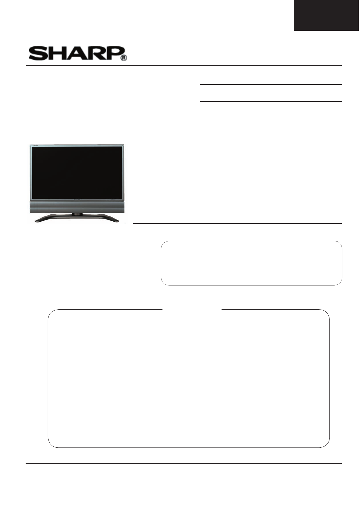
LCD COLOUR TELEVISION
PAL B/G, I / SECAM B/G, D/K, L/L’ SYSTEM COLOUR TELEVISION
MODEL
LC-26GA6E
LC-32GA6E
LC-37GA6E
In the interests of user safety (required by safety
regulations in some countries) the set should be restored to its original condition and only parts identical
to those specifi ed should be used.
E/F/I/K/RU
E/F/I/K/RU
E/F/I/K/RU
LC-26BV6E
LC-32BV6E
CONTENTS
ELECTRICAL SPECIFICATIONS ........................................................................ 3
IMPORTANT SERVICE SAFETY PRECAUTIONS......................................................... 4
DIMENSIONS ......................................................................................................... 6
REMOVING OF MAJOR PARTS .................................................................................... 7
SERVICE ADJUSTMENTS .......................................................................................... 15
SOFTWARE UPDATING ........................................................................................... 29
TROUBLESHOOTING TABLE ............................................................................................ 41
CHASSIS LAYOUT ......................................................................................................... 58
MAJOR ICs INFORMATION .................................................................................................. 60
REPLACEMENT PARTS LIST ........................................................................................................ 89
MECHANICAL PARTS .................................................................................................................... 149
PACKING OF THE SET ................................................................................................................. 155
SOURCE OF DOCUMENTATION ..................................................................................................... 158
BLOCK DIAGRAMS ................................................................................................. 159
OVERALL WIRING DIAGRAM ................................................................................................ 163
SCHEMATIC DIAGRAMS .........................................................................................164
PRINTED WIRING BOARDS ....................................................................................... 202
SHARP CORPORATION
1
This document has been published to
be used for after sales service only.
Page 2

LC-26GA6E/LC-26BV6E
LC-26GA5E
LC-32GA6E/LC-32BV6E
LC-32GA5E
LC-37GA6E
SERVICE MANUAL UPDATE LOG SHEET
Technical Report No.
Technical Bulletin No.
Cause / Solution
Part No.
Page No.
Application
Data /Serial No.
Use this page to keep any special servicing information as Technical Report (Bulletin), Technical Information, etc.
If only part number changes are required, just change part number directly the part number in the Parts Listing Section.
If you need more information, please refer to the Technical Report (Bulletin).
2
Page 3
ELECTRICAL SPECIFICATIONS
LC-26GA6E/LC-26BV6E
LC-26GA5E
LC-32GA6E/LC-32BV6E
LC-32GA5E
LC-37GA6E
Item
LCD panel
Number of dots 3,147,264 dots (1366 g 768 g 3 dots)
Video Colour System PAL/SECAM/NTSC 3.58/NTSC 4.43/PAL 60
TV
Function
FM RADIO
Function
Brightness 450 cd/m
Backlight life 60,000 hours (at Backlight Standard position)
Viewing angles H : 170° V : 170°
Audio amplifier 10W g 2
Speakers Ø 8 cm 2pcs
Terminals
OSD language English/German/French/Italian/Spanish/Dutch/Swedish/Portuguese/Finnish/Turkish/Greek/
Power Requirement AC 220–240 V, 50 Hz
Power Consumption 110 W (0.8 W Standby)
Weight
TV-Standard (CCIR)
Receiving
Channel
TV-Tuning System
STEREO/BILINGUAL NICAM/A2
Receiving Frequency:
Radio-Tuning System:
VHF/UHF E2–E69ch, F2–F69ch, I21–I69ch, IR A–IR Jch
CATV
Rear
Antenna in
FM Radio in
EXT 1
EXT 2
EXT 3 S-VIDEO (Y/C input), RCA pin (AV input)
EXT 4 RCA pin (component input), Ø 3.5 mm Jack (Audio Input)
EXT 5 HDMI (Digital AV input), Ø 3.5 mm jack (Audio input)
PC INPUT D-sub 15 pin (ANALOG RGB), Ø 3.5 mm Jack (Audio Input)
AV OUTPUT
Headphones
26o
LCD COLOUR TV,
Model: LC-26GA6E
26o Advanced Super View &
BLACK TFT LCD
B/G, I, D/K, L, L’
Hyper-band, S1–S41ch
Auto Preset 99 ch, Auto Label, Auto Sort
87.5-108 MHz
Auto Preset 99 ch, Auto Label, Auto Sort
2
UHF/VHF 75 q Din type
Din type
SCART (AV input/output, Y/C input, RGB input, TV output)
SCART (AV input/output, Y/C input, AV Link)
RCA pin (Variable/Fixed)
Ø 3.5 mm jack (Audio output)
Russian/Polish
(Method IEC60107)
12 kg (Display only),
15 kg (Display with stand)
32o
LCD COLOUR TV,
Model: LC-32GA6E
32o Advanced Super View &
BLACK TFT LCD
135 W (0.8 W Standby)
(Method IEC60107)
15.5 kg (Display only),
19.5 kg (Display with stand)
37o
LCD COLOUR TV,
Model: LC-37GA6E
37o Advanced Super View &
BLACK TFT LCD
162 W (0.8 W Standby)
(Method IEC60107)
18.5 kg (Display only),
22.5 kg (Display with stand)
• As a part of policy of continuous improvement, SHARP reserves the right to make design and specification changes for product
improvement without prior notice. The performance specification figures indicated are nominal values of production units. There may
be some deviations from these values in individual units.
NOTE:
The LC-26BV6E and LC-32BV6E models are the same that LC-26GA6E and LC-32GA6E
except the mechanical parts (See page 150 and 152).
3
Page 4
LC-26GA6E/LC-26BV6E
LC-26GA5E
LC-32GA6E/LC-32BV6E
LC-32GA5E
LC-37GA6E
IMPORTANT SERVICE SAFETY PRECAUTION
Service work should be performed only by qualifi ed service technicians who are thoroughly familiar with all
safety checks and the servicing guidelines which follow:
WARNING
1. For continued safety, no modifi cation of any circuit should be attempted.
2. Disconnect AC power before servicing.
CAUTION: FOR CONTINUED PROTECTION AGAINST A RISK OF FIRE REPLACE
ONLY WITH SAME TYPE
F701 (5A, 250V), F702 (5A, 250V), F703 (2A, 250V), F704 (2A, 250V), F705 (1A).
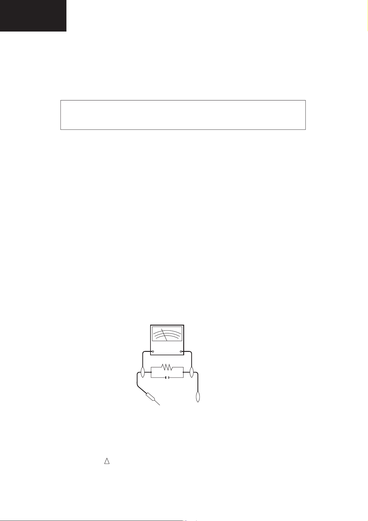
BEFORE RETURNING THE RECEIVER (Fire & Shock Hazard)
Before returning the receiver to the user, perform the following safety checks:
1. Inspect all lead dress to make certain that leads are not pinched, and check that hardware is not lodged between the
chassis and other metal parts in the receiver.
2. Inspect all protective devices such as non-metallic control knobs, insulation materials, cabinet backs, adjustment and
compartment covers or shields, isolation resistor-capacitor networks, mechanical insulators, etc.
3. To be sure that no shock hazard exists, check for leakage current in the following manner.
• Plug the AC cord directly into a 220~240 volt AC outlet. (Do not use an isolation transformer for this test).
•Using two clip leads, connect a 1.5k ohm, 10 watt resistor paralleled by a 0.15μF capacitor in series with all exposed metal
cabinet parts and a known earth ground, such as electrical conduit or electrical ground connected to an earth ground.
•A true RMS reading multimeter should be used for this test, especially where the equipment uses a switch mode
power supply which may result in very non-sinusoidal leakage current.
•Connect the resistor connection to all exposed metal parts having a return to the chassis (antenna, metal cabinet,
screw heads, knobs and control shafts, escutcheon, etc.) and measure the AC voltage drop across the resistor.
All checks must be repeated with the AC cord plug connection reversed. (If necessary, a nonpolarized adaptor plug must
be used only for the purpose of completing these checks.)
Any reading of 0.75V peak (this corresponds to 0.5 mA. peak AC.) or more is excessive and indicates a potential shock
hazard which must be corrected before returning the monitor to the owner.
DVM
AC SCALE
1.5k ohm
10W
0.15 µF
TEST PROBE
TO EXPOSED
METAL PARTS
CONNECT TO
KNOWN EARTH
GROUND
SAFETY NOTICE
Many electrical and mechanical parts in LCD television have special safety-related characteristics.
These characteristics are often not evident from visual inspection, nor can protection afforded by them be necessarily
increased by using replacement components rated for higher voltage, wattage, etc.
Replacement parts which have these special safety characteristics are identifi ed in this manual; electrical components having
such features are identifi ed by “ “ and shaded areas in the Replacement Parts Lists and Schematic Diagrams.
!
For continued protection, replacement parts must be identical to those used in the original circuit.
The use of a substitute replacement parts which do not have the same safety characteristics as the factory recommended
replacement parts shown in this service manual, may create shock, fi re or other hazards.
4
Page 5
LC-26GA6E/LC-26BV6E
L Fa
LC-26GA5E
LC-32GA6E/LC-32BV6E
LC-32GA5E
LC-37GA6E
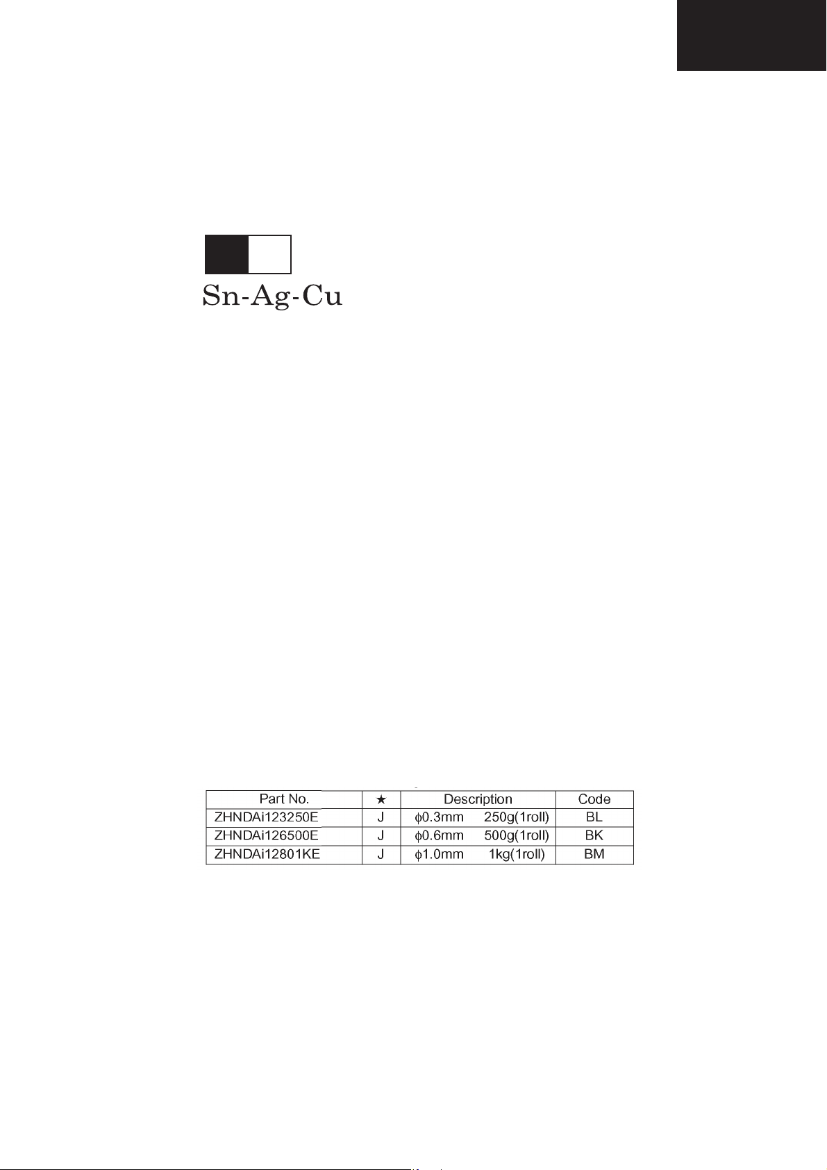
PRECAUTIONS FOR USING LEAD-FREE SOLDER
1 Employing lead-free solder
“ALL PWB” of this model employs lead-free solder. The LF symbol indicates lead-free solder, and is attached on the
PWBs and service manuals. The alphabetical character following LF shows the type of lead-free solder.
Example:
Indicates lead-free solder of tin, silver and copper.
2 Using lead-free wire solder
When fi xing the PWB soldered with the lead-free solder, apply lead-free wire solder. Repairing with conventional lead
wire solder may cause damage or accident due to cracks.
As the melting point of lead-free solder (Sn-Ag-Cu) is higher than the lead wire solder by 40°C, we recommend you to
use a dedicated soldering bit, if you are not familiar with how to obtain lead-free wire solder or soldering bit, contact our
service station or service branch in your area.
3 Soldering
As the melting point of lead-free solder (Sn-Ag-Cu) is about 220°C which is higher than the conventional lead solder by
40°C, and as it has poor solder wettability, you may be apt to keep the soldering bit in contact with the PWB for extended
period of time. However, Since the land may be peeled off or the maximum heat-resistance temperature of parts may be
exceeded, remove the bit from the PWB as soon as you confi rm the steady soldering condition.
Lead-free solder contains more tin, and the end of the soldering bit may be easily corroded. Make sure to turn on and
off the power of the bit as required.
If a different type of solder stays on the tip of the soldering bit, it is alloyed with lead-free solder. Clean the bit after every
use of it.
When the tip of the soldering bit is blackened during use, fi le it with steel wool or fi ne sandpaper.
Be careful when replacing parts with polarity indication on the PWB silk.
Lead-free wire solder for servicing.
5
Page 6
LC-26GA6E/LC-26BV6E
LC-26GA5E
LC-32GA6E/LC-32BV6E
LC-32GA5E
LC-37GA6E
LC-26/32/37GA6E
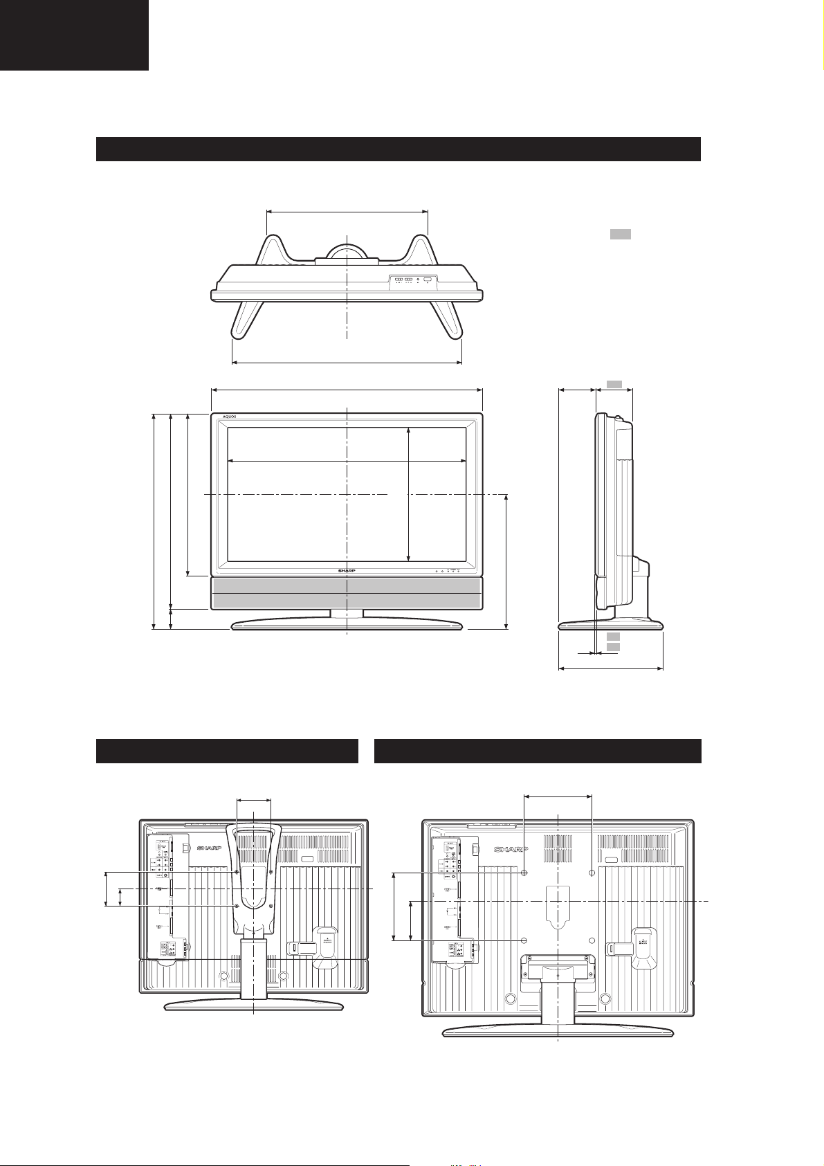
DIMENSIONS
(421) / [473] / ((473))
( ) : LC-26GA6E
[ ] : LC-32GA6E
(( )) : LC-37GA6E
: LC-26/32/37
GA6E
(519) / [677] / ((677))
(663) / [795] / ((917))
(567.9) / [700.4] / ((822.6))
(567,9) / [700,4] / ((822,6))
(407) / [479] / ((548))
(504) / [576] / ((645))(52) / [62] / ((62))
(556) / [638] / ((707))
(320,6) / [395,1] / ((463,8))
(320.6) / [395.1] / ((463.8))
LC-26GA6E LC-32/37GA6E
(355) / [400] / ((435))
(57) /
[109] /
108
((109))
3.1
3,1
(278) / [307] / ((307))
(100)
(50)
(100)
[200] / ((200))
[200] / ((200))
[115] / ((104))
6
Page 7
()
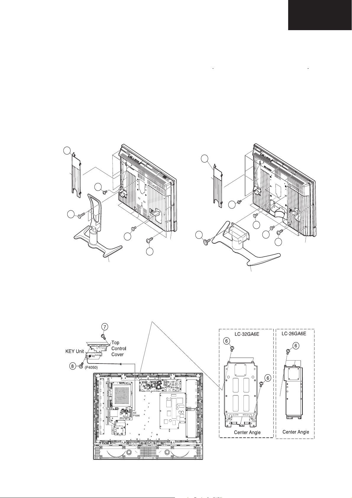
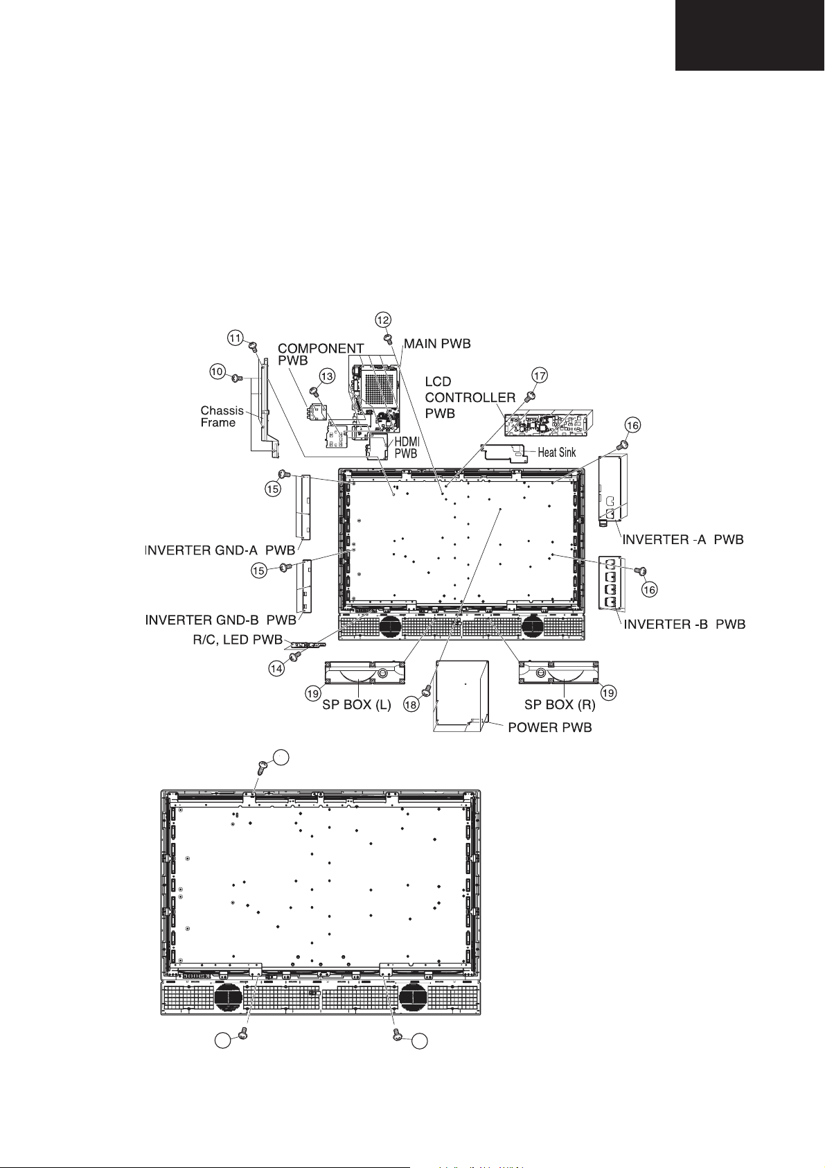
REMOVING OF MAJOR PARTS
LC-26GA6E and LC32GA6E Models
(LC-26GA6E)
1. Remove the Terminal Cover 1 .
2. Remove the 4 lock screws 2 and detach the Stand.
3. Remove the 2 lock screws 3 and the 3 lock screws 4.
4. Remove the 13 lock screws 5 from the Rear Cabinet, and detach the Rear Cabinet.
(LC-32GA6E)
1. Remove the Terminal Cover 1 .
2. Remove the 4 lock screws 2 and detach the Stand.
3. Remove the 4 lock screws 3 and the 3 lock screws 4.
4. Remove the 15 lock screws 5 from the Rear Cabinet, and detach the Rear Cabinet.
1
LC-26GA6E/LC-26BV6E
LC-26GA5E
LC-32GA6E/LC-32BV6E
LC-32GA5E
LC-37GA6E
1
Terminal
Cover
4
2
3
Rear Cabinet
5
Stand
Terminal
Cover
2
4
3
3
5
Stand
(LC-26GA6E) (LC-32GA6E)
5. Remove the 4 (LC-26GA6E) / 7 (LC-32GA6E) lock screws 6 and detach the Center Angle.
6. Remove the KEY Unit.
6-1. Remove the 2 lock screws 7 from the Top Control Cover.
6-2. Remove the 2 lock screws 8 from the KEY Unit.
Rear Cabinet
7
Page 8
LC-26GA6E/LC-26BV6E
LC-26GA5E
LC-32GA6E/LC-32BV6E
LC-32GA5E
LC-37GA6E
7. Disconnect all the connectors from all the PWBs.
8. Remove the MAIN, HDMI and COMPONENT PWBs.
8-1. Remove the 3 lock screws 9 and the 2 lock screws 0. Detach the Chassis Frame.
8-2. Remove the 8 lock screws q and detach the MAIN PWB and HDMI/COMPONENT unit.
8-3. Remove the 4 lock screws w and detach the COMPONENT PWB from HDMI PWB.
9. Remove the 2 lock screws e and detach the R/C,LED PWB
10. Remove the 3 (LC-26GA6E) / 6 (LC-32GA6E) lock screws r and detach the INVERTER GND PWB.
11. LC-26GA6E : Remove the 4 lock screws t and detach the INVERTER PWB.
LC-32GA6E : Remove the 8 lock screws t and detach the INVERTER-A and INVERTER-B PWBs.
12. Remove the 6 lock screws y and detach the LCD CONTROLLER PWB and Heat Sink.
13. Remove the 6 lock screws u and detach the POWER PWB.
14. Remove the 2 lock screws i and detach theSP BOX (L) and (R). (LC-26GA6E only)
CN7601
P2207
P2205
P2206
SC2001
P7704
SC4651
SC4601
SC4652
P2006
CN706
P7707
CN704
P7705
P2103
P1401
P1901
P2102
P4001
P1001
P1902
P2101
P2201
P1301
P1006
P1003
CN707
8
Page 9

LC-26GA6E/LC-26BV6E
LC-26GA5E
LC-32GA6E/LC-32BV6E
LC-32GA5E
LC-37GA6E
15. Remove the 4 (LC-26GA6E) / 3 (LC-32GA6E) lock screws o from the LCD panel unit ass’y, and detach the LCD
panel unit ass’y.
LC-32GA6E
19
LC-26GA6E
19
19
19
LC-32GA6E LC-32GA6E
LC-26GA6E
19
9
Page 10
LC-26GA6E/LC-26BV6E
()
LC-26GA5E
LC-32GA6E/LC-32BV6E
LC-32GA5E
LC-37GA6E
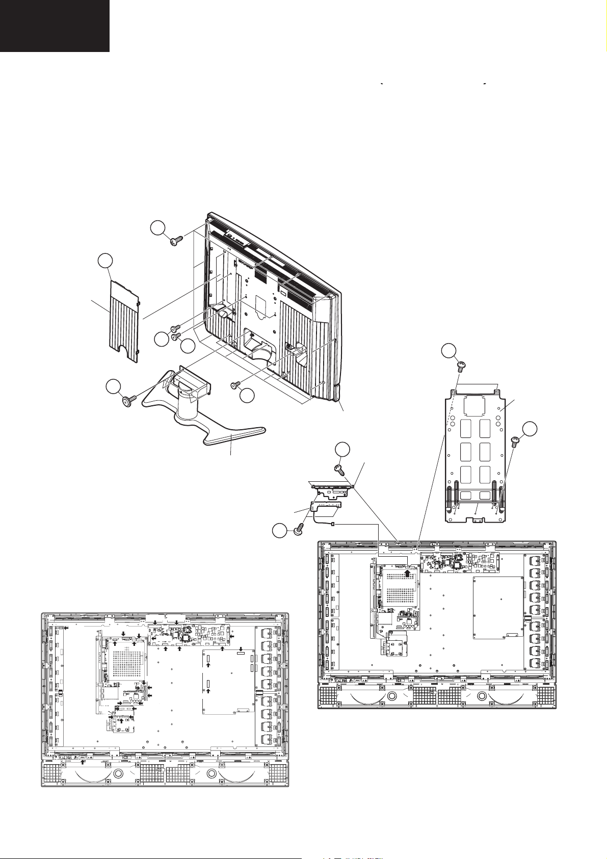
LC-37GA6E Model
1. Remove the Terminal Covers 1.
2. Remove the 4 lock screws 2 and detach the Stand.
3. Remove the 4 lock screws 3, 3 lock screws 4.
4. Remove the 15 lock screws 5 from the Rear Cabinet, and detach the Rear Cabinet.
5. Remove the 2 lock screws 6and the 5 lock screws 7 from the Center Angle, and detach the Center Angle.
6. Remove the KEY PWB.
8-1. Remove the 2 lock screws 8 from the Top Control Cover.
8-2. Remove the 3 lock screws 9 from the KEY PWB.
7. Disconnect all the connectors from all the PWBs.
Terminal
Cover
5
1
CN7601
P2103
P1401
P1901
2
P2205
P2207
P1001
P2101
SC2201
P2206
P1902
P2101
4
SC4651 SC4652
P7704
SC4601
P2201
P1006
P1003
P1301
P2006
3
3
6
Center
Angle
Rear Cabinet
7
8
Stand
Top Control
Cover
KEY Unit
(P4050)
(P1006)
CN706
CN707
P7707
P7705
CN704
9
P4001
10
Page 11
LC-26GA6E/LC-26BV6E
LC-32GA6E/LC-32BV6E
LC-37GA6E
8. Remove the MAIN, COMPONENT and HDMI PWBs.
8-1. Remove the 3 lock screws 0 and the 2 lock screws q. Detach the Chassis Frame.
8-2. Remove the 8 lock screws w and detach the MAIN PWB and HDMI/COMPONENT unit.
8-3. Remove the 4 lock screws e and detach the COMPONENT PWB from HDMI PWB.
9. Remove the 2 lock screws r and detach the R/C,LED PWB
10. Remove the 6 lock screws t and detach the INVERTER GND-A and INVERTER GND-B PWBs.
11. Remove the 8 lock screws y and detach the INVERTER-A and INVERTER-B PWBs.
12. Remove the 6 lock screws u and detach the LCD CONTROLLER PWB and Heat Sink.
13. Remove the 6 lock screws i and detach the POWER PWB.
14. Remove SP BOX (L) and (R) o.
15. Remove the 3 lock screws p from the LCD panel unit ass’y, and detach the LCD panel unit ass’y.
LC-26GA5E
LC-32GA5E
20
20
LCD Panel Unit Ass'y
20
11
Page 12

LC-26GA6E/LC-26BV6E
()
LC-26GA5E
LC-32GA6E/LC-32BV6E
LC-32GA5E
LC-37GA6E
Removing of LCD Panel Unit
LC-26GA6E Model
16. Remove the 4 lock screws p from the 26" LCD Panel Unit, and detach the 26" LCD Panel Unit.
17. Detach the spacers.
18. Detach the Diffusion, Prism and Prism Gurd Sheets and Diffusion Panel.
19. Remove the 6 lock screws a from the Lamp Holder (top), and detach the Lamp Holer (top).
20. Remove the Fluorescent Lamps.
12
Page 13
LC-26GA6E/LC-26BV6E
LC-26GA5E
LC-32GA6E/LC-32BV6E
LC-32GA5E
LC-37GA6E
LC-32GA6E Model
16. Remove the 4 lock screws p from the 32" LCD Panel Unit, and detach the 32" LCD Panel Unit.
17. Detach the sheet spacer-S and sheet spacer-L.
18. Detach the Diffusion, Prism and Prism Gurd Sheets and Diffusion Panel.
19. Remove the 6 lock screws a from the Lamp Holder (top) Ass'y, and detach the Lamp Holer (top) Ass'y.
20. Remove the Fluorescent Lamps.
13
Page 14
LC-26GA6E/LC-26BV6E
LC-26GA5E
LC-32GA6E/LC-32BV6E
LC-32GA5E
LC-37GA6E
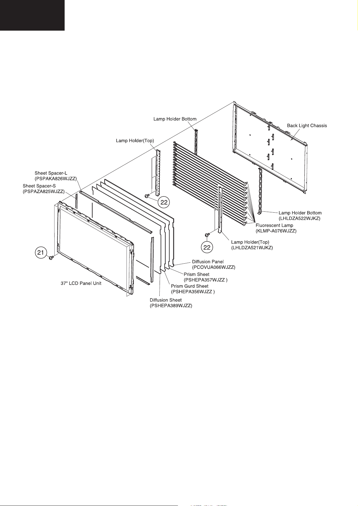
LC-37GA7E Model
16. Remove the 4 lock screws a from the 37" LCD Panel Unit, and detach the 37" LCD Panel Unit.
17. Detach the sheet spacer-L and sheet spacer-S.
18. Detach the Diffusion and Prism Sheets and Diffusion Panel.
19. Remove the 6 lock screws s from the Lamp Holder (top), and detach the Lamp Holder (top).
20. Remove the Fluorescent Lamps.
14
Page 15
Service Adjustments Menus
SERVICE ADJUSTMENTS
LC-26GA6E/LC-26BV6E
LC-26GA5E
LC-32GA6E/LC-32BV6E
LC-32GA5E
LC-37GA6E
VCT PATTERN
GA6 VX.XX ExpX
PATTERN VCT 0
PxW Exp X.X LCD VXX
OPTIONS 0
VCT
PATTERN
OSD
IF
COLOUR OSC OFF
WHITE BALANCE
RGB WHITE BALANCE
W/B PATTERN OFF
OSD
BRIGHTNESS 000
FRC
GA6 VX.XX ExpX
PxW Exp X.X LCD VXX
CTI ON
VOLUME
GA6 VX.XX ExpX
MODE 0
OFFSET 00
IF
GA6 VX.XX ExpX
PxW Exp X.X LCD VXX
CONTRAST 000
RF - AGC OFF
VIDEO AGC
SUBADJ
GA6 VX.XX ExpX
LTI OFF
DCI ON
PxW Exp X.X LCD VXX
BKSH OFF
PATTERN 0
EQUALIZER
PxW Exp X.X LCD VXX
MODE 0
GA6 VX.XX ExpX
BAND 0
VALUE 00
PxW Exp X.X LCD VXX
GA6 VX.XX ExpX
PxW Exp X.X LCD VXX
GA6 VX.XX ExpX
PxW Exp X.X LCD VXX
SUBCONTRAST XXX
SUBBRIGHTNESS XXX
ADC ADJ
SOURCE 0
ADC OFF
VALUE 3
VIDEO-AGC
GA6 VX.XX ExpX
PxW Exp X.X LCD VXX
AGC-AV OFF
AGC MAN 33
M-BASS
WBALANCE
GA6 VX.XX ExpX
PxW Exp X.X LCD VXX
COLOUR 0
WHITE BALANCE
GA6 VX.XX ExpX
PxW Exp X.X LCD VXX
REGISTER 0
VALUE 00
LO 033
HI 175
GAMMA MODE
COPY OFF
RED CUTOFF 000
GREEN CUTOFF 000
BLUE CUTOFF 000
GA6 VX.XX ExpX
RED DRIVE 1FF
GREEN DRIVE 1FF
BLUE DRIVE 1FF
BASS/TREBLE
GA6 VX.XX ExpX
BASS XX
TREBLE XX
ADC MAN
GA6 VX.XX ExpX
PxW Exp X.X LCD VXX
RGB WHITE BALANCE
PxW Exp X.X LCD VXX
OSC OFF
LOUDNESS
PxW Exp X.X LCD VXX
COLOUR 0
GAIN 234
GA6 VX.XX ExpX
PxW Exp X.X LCD VXX
OFFSET 127
SOURCE 0
LOUD MAX 00
FINE ADJ
GA6 VX.XX ExpX
PxW Exp X.X LCD VXX
SAVE
PxW Exp X.X LCD VXX
GA6 VX.XX ExpX
LOUD MIN 00
GAMMA CONST
CONT MIN XXX
CONT MAX XXX
BRI CTR OUT
RED 000
GREEN 000
BLUE 000
BRI MIN XXX
BRI MAX XXX
COL MIN XXX
COL MAX XXX
CONTRAST 255
BRIGHTNESS 255
ACTIVATE OFF
SOURCE 0
COPY LOW OFF
COPY HIGH OFF
GA6 VX.XX ExpX
PxW Exp X.X LCD VXX
GA6 VX.XX ExpX
PxW Exp X.X LCD VXX
GA6 VX.XX ExpX
PxW Exp X.X LCD VXX
VIDEO
VCT
FRC
SHARP SERVICE
VIDEO
GA6 VX.XX ExpX
PxW Exp X.X LCD VXX
FINE ADJ
SUB ADJ
AUDIOPWLCD CONT
NVM
OTHERS
AIS OFF
(Not operative)
AUDIO
VOLUME
EQUALIZER
M_BASS
GA6 VX.XX ExpX
PxW Exp X.X LCD VXX
HOTEL MODE
GA6 VX.XX ExpX
PxW Exp X.X LCD VXX
BASS / TREBLE
LOUDNESS
HOTEL MODE
HOTEL MODE OFF
POWER ON FIXED OFF
M T
PW
PATTERN 0
ADC ADJ
W BALANCE
MAN ADJ
W/B PATTERN OFF
BRI CTR OUT
GAMMA CONST
GA6 VX.XX ExpX
PxW Exp X.X LCD VXX
MAX VOLUME 100
VOLUME FIXED NO
VOL. FIX. VALUE 000
RC BUTTON NO
PANEL BUTTON NO
MENU KEYS NO
OSD NO
IN. MODE START Norm
IN. MODE FIXED NO
LCD CONT
GA6 VX.XX ExpX
PxW Exp X.X LCD VXX
FREQ 0
OTHERS
CPLD
MENU KEYS
STOP BUS
CLR MODE OFF
PATTERN1 00
PATTERN2 0
COMBIAS 190
IC CONT
SOFT VER. XXX
VPS_8/30
GA6 VX.XX ExpX
EXT 2 RGB OFF
FLASH UPGRADE OFF
RAM TEST OFF
COUNTERS
MENU NVM
GA6 VX.XX ExpX
PxW Exp X.X LCD VXX
PxW Exp X.X LCD VXX
ADDR: _ _ _ _
COUNTERS
SW FROM MAINS XXXXX
SW ON TIMES XXXXX
VAL : _ _
SAVE
SW OFF TIMES XXXXX
WORKING HOURS XXXXX
GA6 VX.XX ExpX
HDMI NVM WP YES
ERASE NO
A B C D E F
PxW Exp X.X LCD VXX
GA6 VX.XX ExpX
FAC. DATE DDMY XXXX
PxW Exp X.X LCD VXX
WHITE BALANCE COMPONENT HD
VPS
0300
00
0000
0000
GAMMA R Lo XX
MENU KEYS
GA6 VX.XX ExpX
PxW Exp X.X LCD VXX
ADC1: F5
GAMMA R Lo XX
WHITE BALANCE PC
GA6 VX.XX ExpX
PxW Exp X.X LCD VXX
ADC2: F5
15
Page 16
LC-26GA6E/LC-26BV6E
LC-26GA5E
LC-32GA6E/LC-32BV6E
LC-32GA5E
LC-37GA6E
Adjustment Recomendations
The adjustment values are set to the optimum conditions at the factory before shipping. If a value should become improper
or an adjustment is required due to part replacement, make an adjustment according to the following order:
1. RF AGC (IF Menu). Page 18.
2. Video AGC (IF Menu). Page 18.
3. Colour OSC (VCT Menu). Page 17.
3. Common Bias. (LCD CONT Menu / COMBIAS). Page 24
4. ADC ADJ. Page 22.
5. GAMMA CONST Menu (White Balance Adjustmet). (PW Menu) Page 24.
7. SUBCONTRAST and SUBBRIGHTNESS (VIDEO / SUB ADJ). Page 20.
NOTE: Do not change any other adjust of those above listed, unless you have been advised to do so by a Sharp
representative.
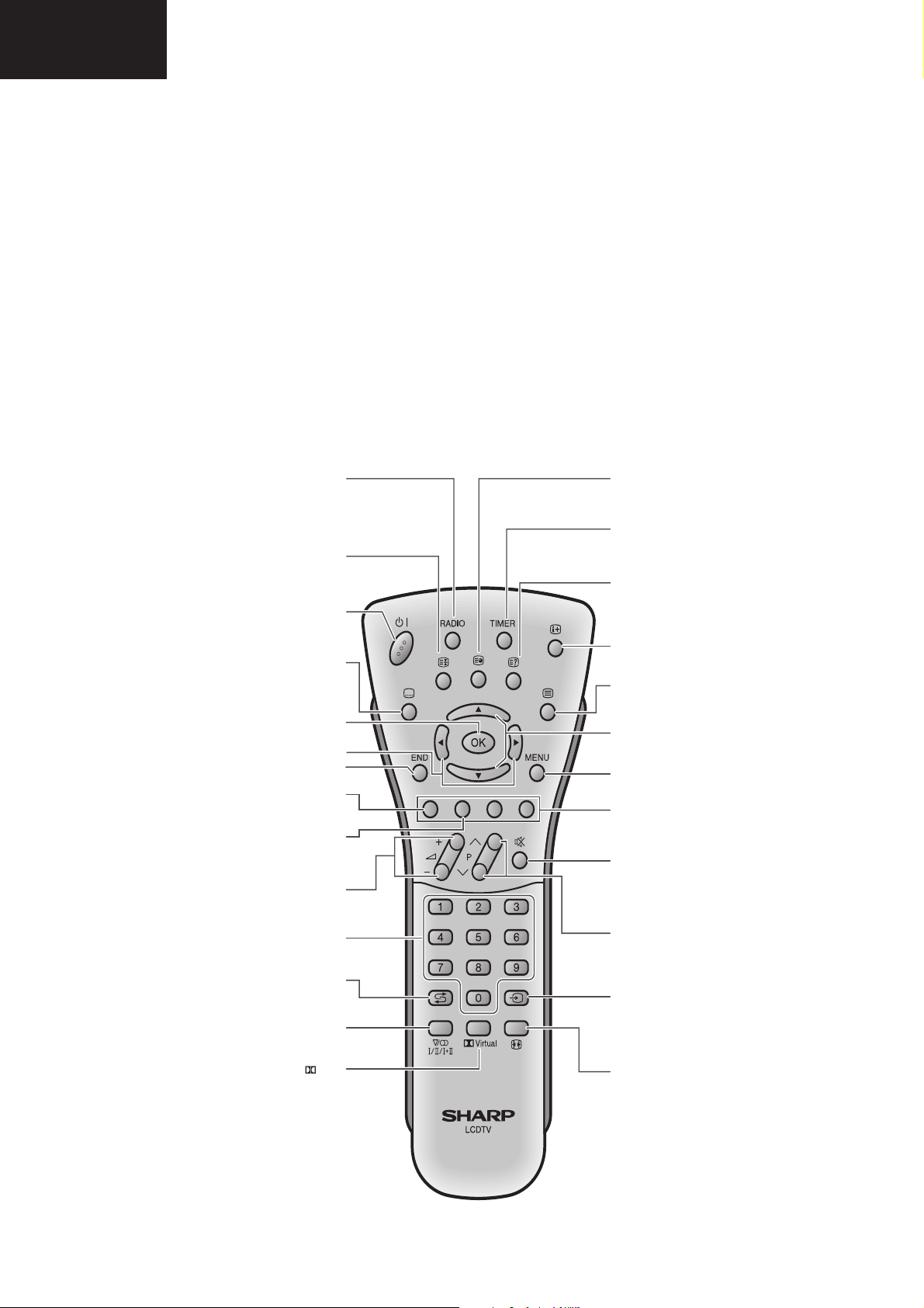
Remote Control Unit
Displays the RADIO MENU screen
and make adjustments for
Temporarily holds the
current Teletext page.
Turns on and off the power or
enters Standby mode.
Go to the next step or execute the
Select a desired level or item.
Displays the “PICTURE LEVELS”
menu directly. (See page 10.)
Displays the “SOUND SPEAKER
LEVELS” menu directly.
i (e/f) (Volume)
i (e) Increases the volume.
i (f) Decreases the volume.
Changes programmes or sets the
page in Teletext mode.
Returns to the previous
programmes or sources.
2 (Sound Mode Selector)
Displays the “STEREO” menu
directly. (See page 12.)
Displays the “SOUND EFFECTS”
menu directly. (See page 11.)
RADIO
FM RADIO mode.
(See page 19.)
3 (Hold)
(See page 20.)
B (Standby/On)
(See page 8.)
[ (Subtitle)
Displays the Teletext
Subtitle directly.
(See page 20.)
OK
item.
Exit the menu item.
Programme select
END
Red
Green
(See page 11.)
A (Flashback)
Virtual
1 (Clock/Subpage)
Displays time in TV mode. (When
available).
Displays the Teletext Subpage in
Teletext mode. (See page 20.)
TIMER
Displays the “FEATURE TIMERS”
menu directly.
(See page 13.)
k (Reveal)
Displays hidden information such
as solutions to riddles and puzzles
in Teletext mode.
(See page 20.)
p (Display/Info)
Displays the programme
information.
m (Teletext)
Displays the Teletext mode screen.
(See page 20.)
Programmes List, Upwards/
Downwards Selection
MENU
Displays the menu. (See page 9.)
Colour (Red/Green/Yellow/Blue)
Select a page in Teletext mode.
(See page 20.)
M (Mute)
Switches the sound on and off.
P (r/s)
r Increases programme number.
s Decreases programme number.
b (Input mode)
Displays “EXT. SOURCES MENU”
menu. (See page 7.)
f (WIDE mode)
Displays the “WIDE MODES” menu
directly, to select your desired
screen size.
(See page 20.)
Sets the area of magnification in
Teletext mode. (See page 20.)
16
Page 17
LC-26GA6E/LC-26BV6E
LC-26GA5E
LC-32GA6E/LC-32BV6E
LC-32GA5E
LC-37GA6E
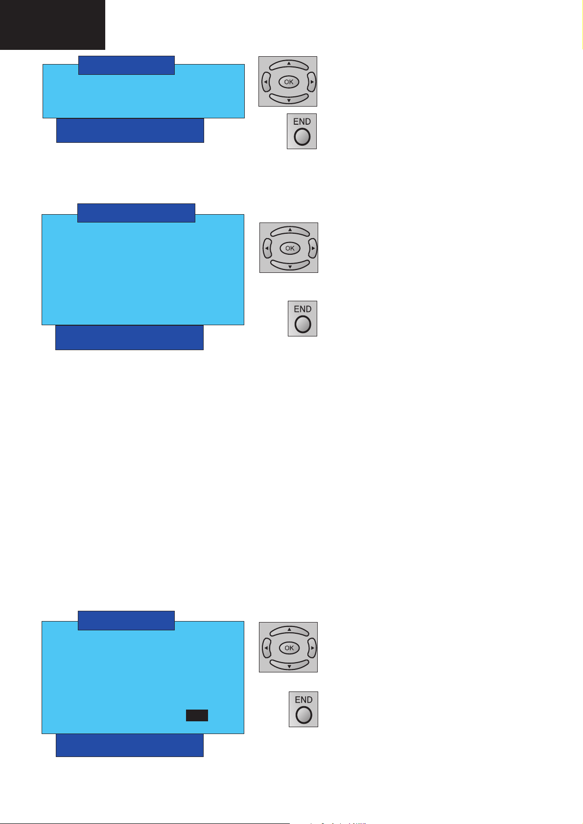
How to enter the Service Mode
The Service Mode is provided to enable the engineer to correctly set up the receiver.
Note that the value of these adjustments may vary from one receiver to another.
Before enter the Service Mode , make factory settings and put the TV in “Dynamic Mode” (Image Mode).
To enter the Service Mode, carry out the following procedure.
1. Connect a test pattern to the antenna terminal.
2. Tune the receiver to this signal.
3. Turn the receiver off using the mains switch.
4. Press volume down and channel up buttons on the top of the receiver at the same time.
5. Keeping these buttons pressed, turn the mains on.
6. Keep pressed the volume down and channel up buttons until the Service Mode On Screen Display (OSD) appears:
SHARP SERVICE
VIDEO
AUDIO
PW
LCD CONT
NVM
OTHERS
AIS OFF
HOTEL MODE
GA6 VX.XX ExpX
PxW Exp X.X LCD VXX
AIS: Autoinstallation.
Video Menu
If you select the VIDEO option the next On Screen Display appear:
VIDEO
VCT
FRC
FINE ADJ
SUBADJ
GA6 VX.XX ExpX
PxW Exp X.X LCD VXX
Use the up/down arrows imprinted on the ring of the
R/C to select a line/term in the menu.
Confi rm the selection with OK this will take you to
the next menu.
Press END button to exit of Service Menu.
Use the up/down arrows to select a term in the
menu.
Confi rm the selection with OK this will take you to
the next menu.
Pressing END button the OSD returns to the
previous menu.
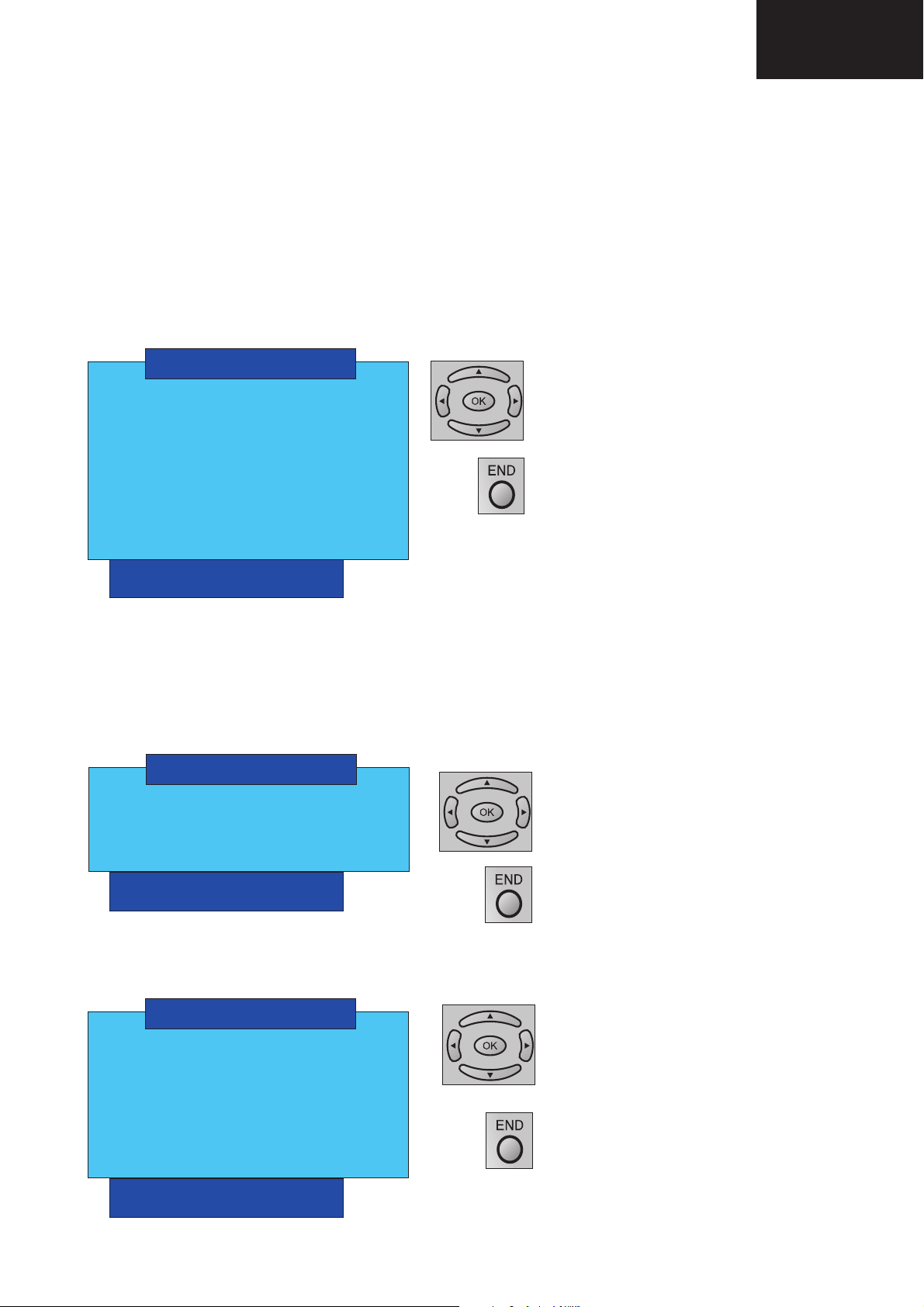
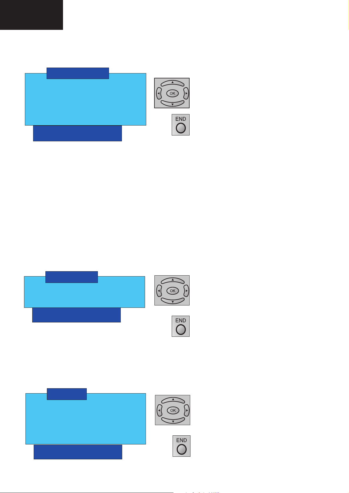
VCT Menu
To adjust parameters of VCT IC.
VCT
PATTERN
OSD
IF
COLOUR OSC OFF
WHITE BALANCE
RGB WHITE BALANCE
W/B PATTERN OFF
GA6 VX.XX ExpX
PxW Exp X.X LCD VXX
Use the up / down arrows to select a term in the
menu.
Confi rm the selection with OK.
COLOUR OSC is adjusting automatically when
is selected.
Pressing END button the OSD returns to the
previous menu.
17
Page 18
LC-26GA6E/LC-26BV6E
LC-26GA5E
LC-32GA6E/LC-32BV6E
LC-32GA5E
LC-37GA6E
VCT PATTERN
PATTERN VCT 0
OPTIONS 0
GA6 VX.XX ExpX
PxW Exp X.X LCD VXX
PATTERN VCT: Contains internal adjusting patterns for VCT IC.
OPTIONS: Changes of colour standards for the patterns. (0,1,2,3)
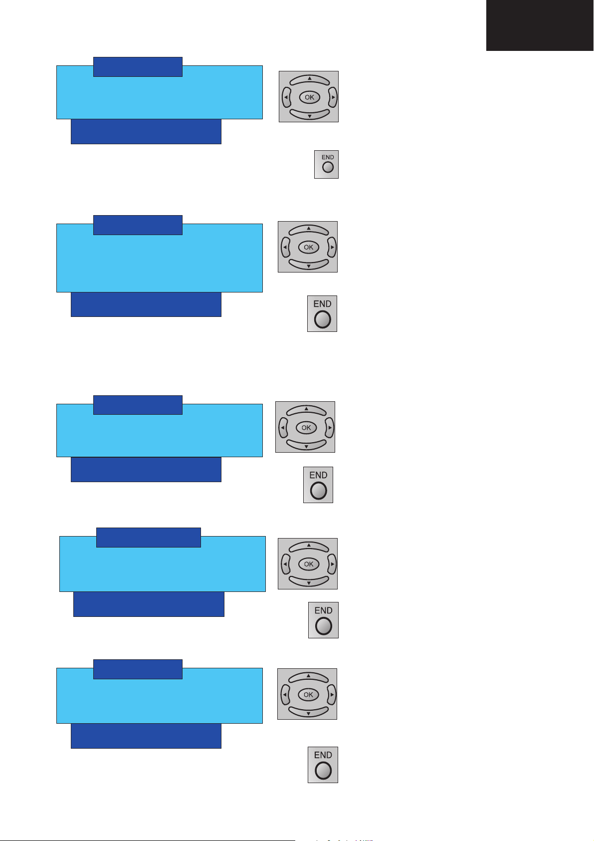
OSD Menu
It allows to change to the brightness and the contrast of the On Screen Display.
OSD
BRIGHTNESS 000
CONTRAST 019
GA6 VX.XX ExpX
PxW Exp X.X LCD VXX
Use the up / down arrows to select a term in the
menu.
Confi rm the selection with OK.
Use the up / down arrows to change pattern.
Press END button to return to the previous menu.
Use the up / down arrows to select a term in the
menu.
Confi rm the selection with OK.
Use the left / right arrows to change between parameters.
Use the up / down arrows to change parameters.
Press END button to return to the previous menu.
IF Menu
Intermediate frequency AGC adjustment. To adjust this item tuning the TV in follow conditions:
- Channel 12
- RF level: 60 dB/uV
- Pattern: Colour bar
IF
RF - AGC OFF
VIDEO AGC
GA6 VX.XX ExpX
PxW Exp X.X LCD VXX
RF-AGC: is adjusting automatically when ON is se-
lected.
The next OSD appear:
ADJ OK!
VIDEO-AGC Menu
Input 1,2,or 3 video input terminal PAL, colour bar with 115% of white.
VIDEO-AGC
AGC-AV OFF
AGC MAN 33
Use the up / down arrows to select a term in the
menu.
Confi rm the selection with OK.
Change between ON/OFF option.
Press END button to return to the previous menu.
Confi rm the selection with OK.
Use the up / down arrows to select between ON/
OFF (It are blinking).
GA6 VX.XX ExpX
PxW Exp X.X LCD VXX
AGC: is adjusting automatically when ON is selected.
The next OSD appear:
ADJ OK!
Press END button to return to the previous menu.
18
Page 19
LC-26GA6E/LC-26BV6E
LC-26GA5E
LC-32GA6E/LC-32BV6E
LC-32GA5E
LC-37GA6E
Colour OSC Menu
To adjust the colour sub-carrier with local oscillator (Adjust for PAL signals). Input 1, 2 or 3 video input terminal PAL
colour bar. The Colour OSC is adjusted automatically when option ON is selected.
When COLOUR OSC is adjusted the next OSD appear:
ADJ OK !
White Balance Menu (It is recomended do not modify)
To adjust the Back Ground (BKGD) of TV.
WHITE BALANCE
RED DRIVE 1FF
GREEN DRIVE 1FF
BLUE DRIVE 1FF
RED CUTOFF 000
GREEN CUTOFF 000
BLUE CUTOFF 000
GA6 VX.XX ExpX
PxW Exp X.X LCD VXX
At TV will appear the factory adjust values.
RGB WHITE BALANCE
RED 32
GREEN 32
BLUE 32
GA6 VX.XX ExpX
PxW Exp X.X LCD VXX
Use the up / down arrows to select a term in the
menu.
Confi rm the selection with OK.
Use the left / right arrows to move between the
parameters.
Use the up / down arrows to change the values.
Confi rm the selection with OK.
Press END button to return to the previous menu.
Use the up / down arrows to select a term in the
menu.
Confi rm the selection with OK.
Use the left / right arrows to move between the
parameters.
Use the up / down arrows to change the values.
Confi rm the selection with OK.
Press END button to return to the previous menu.
FRC Menu
To adjust FRC IC. These parameters are adjusted and saved automatically when the ON option is selected.
FRC
CTI ON
LTI OFF
DCI ON
BKSH OFF
PATTERN 0
GA6 VX.XX ExpX
PxW Exp X.X LCD VXX
CTI: Chroma Transient Improvement
LTI: Luminance Transient Improvement
DCI: Dynamic Contrast Improvement
BKSH: Black Stretcher
PATTERN: Contains internal adjusting patterns for FRC IC.
Use the up / down arrows to select a term in the
menu.
Confi rm the selection with OK.
Use the up / down arrows to change between ON
/ OFF options.
Confi rm the selection with OK.
Pressing END button the OSD returns to the previous menu.
19
Page 20
LC-26GA6E/LC-26BV6E
LC-26GA5E
LC-32GA6E/LC-32BV6E
LC-32GA5E
LC-37GA6E
Fine Adjust Menu
This menu allows to adjust of more precise way the contrast, brightness and colour items. (AtTV will appear the
factory adjust values)
FINE ADJ
CONT MIN XXX
CONT MAX XXX
BRI MIN XXX
BRI MAX XXX
COL MIN XXX
COL MAX XXX
GA6 VX.XX ExpX
PxW Exp X.X LCD VXX
CONT MIN:Fine adjust of minimum contrast.
CONT MAX: Fine adjust of maximum contrast.
BRI MIN: Fine adjust of minimum brightness.
BRI MAX: Fine adjust of maximum brightness.
COL MIN: Fine adjust of minimum colour.
COL MAX: Fine adjust of maximum colour.
Subadjust Menu
With a grey scale (11 bars) adjust the subbrightness and subcontrast. This way the picture will be not saturated in the
end of white and the end of black.
Adjustment
Put backlight at 8 and Contrast at 40.
Increase subcontrast until the second last bar (white 90%) becomes white (100%).
Decrease subcontrast until the penultimate bar (White 90%) becomes visible.
Use the up / down arrows to select a term in the
menu.
Confi rm the selection with OK.
Use the left / right arrows to move between the
parameters.
Confi rm the selection with OK.
Press END button to return to the previous menu.
SUBADJ
SUBCONTRAST XXX
SUBBRIGHTNESS XXX
GA6 VX.XX ExpX
PxW Exp X.X LCD VXX
At TV will appear the factory adjust values.
SUBCONTRAST: Fine adjust of contrast in order to sharpen the adjust the end of white.
SUBRIGHTNESS: Fine adjust of brightness in order to sharpen the adjust the end of black.
Use the up / down arrows to select a term in the
menu.
Confi rm the selection with OK.
Use the left / right arrows to move between the
parameters.
Confi rm the selection with OK.
Press END button to return to the previous menu.
Audio Menu (Not operative)
AUDIO
Use the up / down arrows to select a term in the
VOLUME
EQUALIZER
M_BASS
BASS/TREBLE
LOUDNESS
GA6 VX.XX ExpX
PxW Exp X.X LCD VXX
menu.
Confi rm the selection with OK.
Press END button to return to the previous menu.
20
Page 21
VOLUME
MODE 0
OFFSET 00
GA6 VX.XX ExpX
PxW Exp X.X LCD VXX
LC-26GA6E/LC-26BV6E
LC-26GA5E
LC-32GA6E/LC-32BV6E
LC-32GA5E
LC-37GA6E
Use the up / down arrows to select a term in the
menu.
Confi rm the selection with OK.
Use the up / down arrows to change values.
Confi rm the selection with OK.
MODE: MONO, STEREO, DOLBY, PANORAMA
OFFSET: Value of compensation according to mode.
EQUALIZER
MODE 0
BAND 0
VALUE 00
GA6 VX.XX ExpX
PxW Exp X.X LCD VXX
MODE: Not operative.
BAND: Choose the equalizer band.
VALUE: Offset added to the center point of the selected band.
M-BASS
REGISTER 0
VALUE 00
GA6 VX.XX ExpX
PxW Exp X.X LCD VXX
Press END button to return to the previous menu.
Use the up / down arrows to select a term in the
menu.
Confi rm the selection with OK.
Use the up / down arrows to change values.
Confi rm the selection with OK.
Press END button to return to the previous menu.
Use the up / down arrows to select a term in the
menu.
Confi rm the selection with OK.
Use the up / down arrows to change values.
Confi rm the selection with OK.
Press END button to return to the previous menu.
Parameters to adjust M-BASS features.
BASS/TREBLE
BASS XX
TREBLE XX
GA6 VX.XX ExpX
PxW Exp X.X LCD VXX
LOUDNESS
LOUD MAX 00
LOUD MIN 00
GA6 VX.XX ExpX
PxW Exp X.X LCD VXX
Maximum and minimum values of LOUD.
Use the up / down arrows to select a term in the
menu.
Confi rm the selection with OK.
Use the up / down arrows to change values.
Confi rm the selection with OK.
Press END button to return to the previous menu.
Use the up / down arrows to select a term in the
menu.
Confi rm the selection with OK.
Use the up / down arrows to change values.
Confi rm the selection with OK.
Press END button to return to the previous menu.
21
Page 22
LC-26GA6E/LC-26BV6E
LC-26GA5E
LC-32GA6E/LC-32BV6E
LC-32GA5E
LC-37GA6E
PW Menu
To check the PW IC.
PW
PATTERN 0
ADC ADJ
W BALANCE
MAN ADJ
W/B PATTERN OFF
BRI CTR OUT
GAMMA CONST
GA6 VX.XX ExpX
PxW Exp X.X LCD VXX
PATTERN: Internal pattern of PW to check the IC.
ADC Adjust (Operative from: VCTi 96 / PW 58 software version and upper)
ADC ADJ
SOURCE 0
ADC OFF
VALUE 3
GA6 VX.XX ExpX
PxW Exp X.X LCD VXX
Use the up / down arrows to select a term in the
menu.
Confi rm the selection with OK.
Press END button to return to the previous menu.
Use the up / down arrows to select a term in the
menu.
Confi rm the selection with OK.
Use the up / down arrows to change between options.
Confi rm the selection with OK.
Press END button to return to the previous menu.
SOURCE: TV, PC, Components
ADC: is adjusting automatically when ON is selected.
The next OSD appear:
SAVED
Adjustments
Source 0: Video Composite
Input video: Not necessary
Select ADC item. When confi rm selection with OK , OFF is fl ashing. Press the up arrow one time, and the adjust
made automatically.
Source 1: PC
Input PC signal.
Pattern: Grey scale, 10 steps
Format: XGA (1024 x 768 @ 60Hz).
Use the up arrow menu to select source 1. Confi rm the selection with OK. Use the up arrow menu to select ADC.
Confi rm selection with OK, OFF is fl ashing. Touch the up arrow one time, and the adjust made automatically.
Source 2: Component 720p.
Input component signal.
Pattern: Grey scale, 10 steps.
Format: 720p / 50Hz.
Use the up arrow menu to select source 2. Confi rm the selection with OK. Use the up arrow menu to select ADC.
Confi rm the selection with OK. Off is fl ashing. Touch the up arrow one time, and the adjust made automatically.
22
Page 23
LC-26GA6E/LC-26BV6E
LC-26GA5E
LC-32GA6E/LC-32BV6E
LC-32GA5E
LC-37GA6E
Source 3: Component 1080i.
Input component signal.
Pattern: Grey scale, 10 steps.
Format: 1080i / 60Hz.
Use the up arrow menu to select source 3. Confi rm the selection with OK. Use the up arrow menu to select ADC.
Confi rm the selection with OK. Off is fl ashing. Touch the up arrow one time, and the adjust made automatically.
WBalance Menu (It is recomended for WB adjust use GAMMA CONST Menu).
White Balance adjust of TV mode. Before to carry out the White Balance Adjustments, it is requested to achieve
the Common bias and ADC adjustments in this order.
WBALANCE
COLOUR 0
LO 033
HI 175
GAMMA MODE
COPY OFF
GA6 VX.XX ExpX
PxW Exp X.X LCD VXX
LO / HI: adjusting points to 20% and 80% of colour saturation.
Adjustment
Input 1, 2 or 3 video input terminal.
Pattern: White 20%.
Brightness and contrast: Dynamic settings.
Change LO value in «COLOUR 0» (red) and «COLOUR 2» (blue) in order to become the reference value. Repeat as far as reference level is required.
Do not change green colour (1). It must be as default value.
Change pattern White 80%.
Change HI value in «COLOUR 0» (red) and «COLOUR 2» (blue) in order to become the reference value. Repeat as far as reference level is required.
Do not change green colour (1). It must be as default value.
Use the up / down arrows to select a term in the
menu.
Confi rm the selection with OK.
Use the up / down arrows to change values.
Use the left / right arrows to change between parameters.
Press END button to return to the previous menu.
GAMMA MODE: Differentiate between two types of gamma. (It is recomended do not modify)
ADC MAN Menu
Manual adjust of PixelWorks Analog Digital Converter. Only for look the adjustment value.(It is recomended do not
modify)
Use the up / down arrows to select a term in the
ADC MAN
COLOUR 0
GAIN 234
OFFSET 127
SOURCE 0
GA6 VX.XX ExpX
PxW Exp X.X LCD VXX
BRI CTR OUT Menu
Brightness and contrast output that affects to OSD and picture at the same time.
menu.
Confi rm the selection with OK.
Use the up / down arrows to change values.
Use the left / right arrows to change between parameters.
Press END button to return to the previous menu.
23
Page 24
LC-26GA6E/LC-26BV6E
LC-26GA5E
LC-32GA6E/LC-32BV6E
LC-32GA5E
LC-37GA6E
BRI CTR OUT
CONTRAST 255
BRIGHTNESS 255
GA6 VX.XX ExpX
PxW Exp X.X LCD VXX
GAMMA CONST Menu (White Balance Adjustment)
Fine and manual adjustment of gamma with patterns done defi ning the values of R, G, B.
Use the up / down arrows to select a term in the
menu.
Confi rm the selection with OK.
Use the up / down arrows to change values.
Use the left / right arrows to change between parameters.
Press END button to return to the previous menu.
GAMMA CONST
Use the up / down arrows to select a term in the
RED 000
GREEN 000
BLUE 000
ACTIVATE OFF
SOURCE 0
COPY LOW OFF
COPY HIGH OFF
GA6 VX.XX ExpX
PxW Exp X.X LCD VXX
menu.
Confi rm the selection with OK.
Use the up / down arrows to change values.
Use the left / right arrows to change between parameters.
Press END button to return to the previous menu.
ACTIVATE: It activates the pattern previously selected.
SOURCE: Choose between 0(TV), 1(PC) or 2(HD).
COPY LOW: Saves in NVM the adjusting point of gamma. (Black pattern: 20% of white)
COPY HIGH: Saves in NVM the adjusting point of gamma. (White pattern: 80% of white)
Adjust:
- In order to obtain a pattern with a 20% of white, set to 63 the values of RGB.
- Choose ACTIVATE option and press OK.
- Measure with the colorimeter the white intensity of pattern.
- Press again OK key to return GAMMA CONST Menu.
- Change red or blue to obtained the 20% of white temperature. (Green must be the reference value, so do not
change)
- Finally, already obtained the correct value, save 20% of white with “COPY LOW”.
- Change the source to 1 (PC) and press “COPY LOW” again, change source to 2(HD) and press “COPY LOW”
once more.
Thereby, the same colour temperature is copied at all the sources.
- To obtain a pattern with 80% of white, set to 200 the RGB values and repeat the process before described
pressing fi nally, “COPY HIGH” instead “COPY LOW”.
LCD Cont Menu
Panel control (QS board adjustments).
LCD CONT
FREQ 0
CLR MODE OFF
PATTERN1 00
PATTERN2 0
COMBIAS 190
IC CONT
SOFT VER. XXX
Use the up / down arrows to select a term in the
menu.
Confi rm the selection with OK.
Using the up / down arrows the values are
changed.
Press END button to return to the previous menu.
GA6 VX.XX ExpX
PxW Exp X.X LCD VXX
24
Page 25
LC-26GA6E/LC-26BV6E
LC-26GA5E
LC-32GA6E/LC-32BV6E
LC-32GA5E
LC-37GA6E
FREQ: Change between 50/60Hz and PC.
CLR MODE: When press OK key send the value to monitor microcontroller.
PATTERN1: Choose pattern to adjust QS.
PATTERN2: Choose pattern to adjust QS.
COMBIAS: Specifi c adjustment for QS. COMMON BIAS adjusting value is displayed.
IC CONT: See the next OSD.
SOFT VER.: Software version of QS IC. Display the version of monitor microcontroller.
COMBIAS Adjustment
Select COMBIAS and press the “OK” button so that the fl icker screen will appear.
Adjust the fl icker on the screen to minimum with up / down buttons on the remote control. At this time, press the “OK”
key to complete the adjustment.
IC Cont Menu (NOT OPERATIVE)
Send specifi c data to the QS board.
IC CONT
DEVICE 0
ADDR 000
DATA 00
R/W OFF/ON
SEND
GA6 VX.XX ExpX
PxW Exp X.X LCD VXX
DEVICE: To select QS peripherals ICs. ( 0:LCD Controller / 1:QS Driver / 2: Extended Digital Analog Converter /
3: EEprom Microcontroller / 4: Reserved)
ADDR: Address of register.
DATA: Read mode: Display data after executing “SEND” / Write mode: Select data to write.
R/W: Select Read or Write. ON: write OFF: read.
SEND: Send data to QS.
Use the up / down arrows to select a term in the
menu.
Confi rm the selection with OK.
Use the up / down arrows to change values.
Use the left / right arrows to change between parameters.
Press END button to return to the previous menu.
NVM Menu
To change NVM values.
MENU NVM
Use the up / down arrows to select a term in the
ADDR: _ _ _ _
VAL : _ _
SAVE
HDMI NVM WP YES
ERASE NO
A B C D E F
menu.
Confi rm the selection with OK.
Use the left / right arrows to change between parameters.
Use the up / down arrows to change values.
M T
GA6 VX.XX ExpX
PxW Exp X.X LCD VXX
Press END button to return to the previous menu.
ADDR: NVM address.
VAL: NVM Value.
SAVE: Save NVM changes.
HDMI NVM WP: Unprotect the EDID, that contains the recognizable formats of screen for HDMI.
ERASE: If you select YES and Turn OFF-ON the TV by main switch, the data of NVM will be recorded
to the default values .
In ADDR option of this menu, by using the colour buttons of R/C is possible to pass directly to A, B, C or D parameter.
Note: DO NOT change any NVM data, unless you have been advised to do by a Sharp representative. If data is
incorrectly changed, serious damage may occur to the receiver.
25
Page 26
LC-26GA6E/LC-26BV6E
LC-26GA5E
LC-32GA6E/LC-32BV6E
LC-32GA5E
LC-37GA6E
OTHERS
Use the up / down arrows to select a term in the
CPLD
MENU KEYS
STOP BUS
VPS_8/30
EXT 2 RGB OFF
FLASH UPGRADE OFF
RAM TEST OFF
COUNTERS
GA6 VX.XX ExpX
PxW Exp X.X LCD VXX
CPLD: NOT OPERATIVE
STOP BUS: Stop IC communication.
EXT 2 RGB: Enable or disable the RGB entry over EXT2 connector.
FLASH UPGRADE: Select ON to update to software update. (See page 23)
RAM TEST: Check the RAM memory. It is working correctly when “OFF” appear on the screen. If any number appear,
the memory is not working correctly.
Counters Menu
To see information about TV.
menu.
Confi rm the selection with OK.
Press END button to return to the previous menu.
COUNTERS
SW FROM MAINS XXXXX
SW ON TIMES XXXXX
SW OFF TIMES XXXXX
WORKING HOURS XXXXX
FAC. DATE DDMY XXXX
GA6 VX.XX ExpX
PxW Exp X.X LCD VXX
SW FROM MAINS: Number of times that turn on the TV by the main switch.
SW ON TIMES: Number of times that switch on the TV by the R/C.
SW OFF TIMES: Number of times that switch on the TV by the R/C.
WORKING HOURS: Number of hours that is working the TV.
FAC. DATE DDMY: TV manufacture date (day, month, year).
KEYS Menu
Control menu of good operation of the top panel control keys.
If, when a key of the panel is pressed, the value who appears is within the parameters that appear in this menu, the
operation of this key is correct. High values near FF means, no key pressed.
Press END button to return to the previous menu.
MENU KEYS
ADC1: F5
ADC2: F5
GA6 VX.XX ExpX
PxW Exp X.X LCD VXX
Press END button to return to the previous menu.
26
Page 27
VPS Menu
Broadcasting code identifi cation.
VPS
0300
00
0000
0000
GA6 VX.XX ExpX
PxW Exp X.X LCD VXX
HOTEL Menu
In this menu the Hotel Mode is activated or deactivated.
LC-26GA6E/LC-26BV6E
LC-26GA5E
LC-32GA6E/LC-32BV6E
LC-32GA5E
LC-37GA6E
Only information about VPS. Changes are not allowed.
MENU HOTEL
HOTEL MODE OFF
POWER ON FIXED OFF
MAX VOLUME 100
VOLUME FIXED NO
VOL. FIX. VALUE 000
RC BUTTON NO
PANEL BUTTON NO
MENU KEYS NO
OSD NO
IN. MODE START Norm
IN. MODE FIXED NO
GA6 VX.XX ExpX
PxW Exp X.X LCD VXX
HOTEL MODE : To activate or to deactivate the HOTEL MODE.
POWER ON FIXED: Disable power on/off button of remote control.
MAX VOLUME : To limit the maximum volume.
VOLUME FIXED: Fix volume level.
VOL. FIX. VALUE: Value of “VOLUME FIXED”
RC BUTTON: To activate or to deactivate all remote control keys.
PANEL BUTTON: Disable all buttons on the main unit.
MENU KEYS: Disable “MENU” button on main unit and remote control.
OSD: Disable the OSD displaying.
IN. MODE START: Specify starting channel when power button is switched.
IN. MODE FIXED: Allows start with the input specifi ed in “INPUT MODE START” and prohibit to change channel
and input.
Confi rm the selection with OK.
Use the up / down arrows to change between
ON/OFF.
Press END button to return to the previous menu.
27
Page 28
LC-26GA6E/LC-26BV6E
LC-26GA5E
LC-32GA6E/LC-32BV6E
LC-32GA5E
LC-37GA6E
HD Component White Balance
(
For White Balance adjust it is recomended to use GAMMA CONST menu)
Before to carry out the HD Component White Balance Adjustments, it is requested to achieve the Common bias and
ADC adjustments in this order.
Input Component signal format 720p / 50Hz (Pattern: White 20%.)
Change to EXT 4 in menu TV and set brightness and contrast to 50%.
Enter in adjustment process by remote control ( key). The following OSD appears:
This Key (BROWSE) can be found in many CRT TV
Remote Control. We detail two of them below:
Part Reference SN Price Code EX Price Code
RRMCG0739BMSA AW BT
RRMCG1022BMSA ** BB
GAMMA R Lo XX
By up or down key choose Gamma R Lo or Gamma B Lo and adjust in order to become the reference value. Repeat as
far as reference level is required.Don’t change green colour. It must be as default value.
Change pattern: White 80%.
By up or down key choose Gamma R Hi or Gamma B Hi and adjust in order to become the reference value. Repeat as
far as reference level is required.Don’t change green colour. It must be as default value.
PC White Balance
(For White Balance adjust it is recomended to use GAMMA CONST menu)
Before to carry out the PC White Balance Adjustments, it is requested to achieve the Common bias and ADC adjustments in this order.
Input PC signal format -XGA (Pattern: White 20%.)
Change to PC Input in menu TV and set brightness and contrast to 50%.
Enter in adjustment process by remote control (browse key). The same White Balance Component HD OSD appears.
By up or down key choose Gamma R Lo or Gamma B Lo and adjust in order to become the reference value. Repeat as
far as reference level is required.Don’t change green colour. It must be as default value.
Change pattern: White 80%.
By up or down key choose Gamma R Hi or Gamma B Hi and adjust in order to become the reference value. Repeat as
far as reference level is required.Don’t change green colour. It must be as default value.
28
Page 29
LC-26GA6E/LC-26BV6E
LC-26GA5E
LC-32GA6E/LC-32BV6E
LC-32GA5E
LC-37GA6E
SOFTWARE UPDATING
How to update VCTi Software
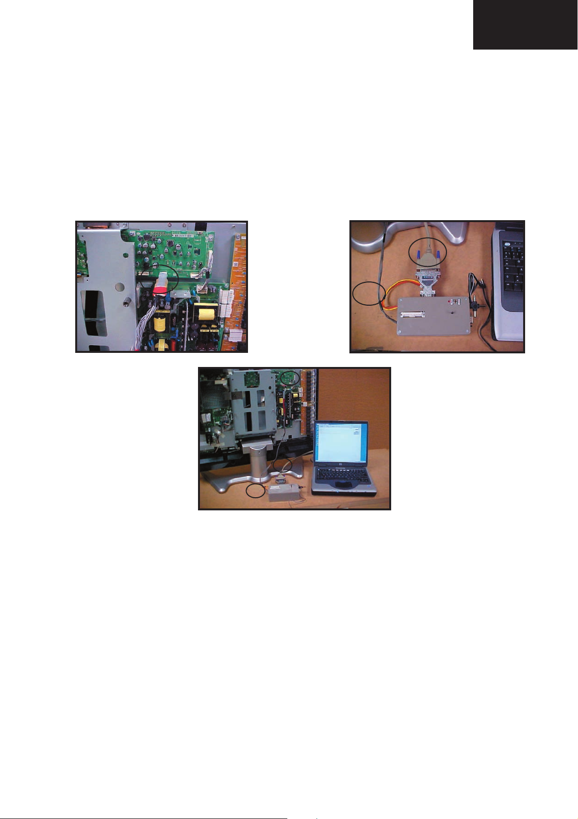
Hardware requirements
To update VCT it is needed:
1. A converter from Parallel port to DB9 supplied by Micronas, a male DB9 to female DB9 wire and the updating
tool (Part Code: CKIT-0002WJV0).
2. Make the connections as indicated below.
2.1. Connect Parallel cable from the updating tool to the PC.
2.2. Connect the long cable from the updating tool to the P2005 connector (LCD Controller PWB).
2.1
2.2
2.2
2.2
2.1
2.2
Software requirements
A complete Visual I2C (VI2C) installation consists of 4 software components:
1. Visual I2C main program (‘visuali2c.exe’ and several DLL fi les)
2. Several DALs: These are IC specifi c low-level access drivers for the I2C bus.
3. A Windows port driver (LPT or USB). There are three versions for Win9x and WinNT/2000/XP.
4. One or more applications (‘*.vi2c’). They’re representing the interface to the user.
Software preparation and update
Access to folder:
-D:\SOFTWARE UPDATE GA5\Installation order VCTi\1
-Install Visual I2C (SETUP_VISUAL_I2C_V3_1_7C.EXE)
It’s strongly recommended to accept the suggested default folder.
29
Page 30
LC-26GA6E/LC-26BV6E
LC-26GA5E
LC-32GA6E/LC-32BV6E
LC-32GA5E
LC-37GA6E
Access to folder:
-D:\SOFTWARE UPDATE GA5\Installation order VCTi\2
-Install LPT driver SETUP_LPTDRVDEV_V0202_XP_20.EXE
Use for Windows 95/98: Setup_LptDrv_v0104_9x.exe
Use for Windows 2000/XP: Setup_LptDrv_v0202_XP_20.exe
Use for Windows NT: Setup_LptDrv_v0104_NT.exe
After installing VI2C, the new generated fi le structure should look like this:
—> Micronas
|—> LptDrv (in case of parallel port driver installed!)
|—> Visual I2C
|—> dal
|—> doc
|—> Port_Driver
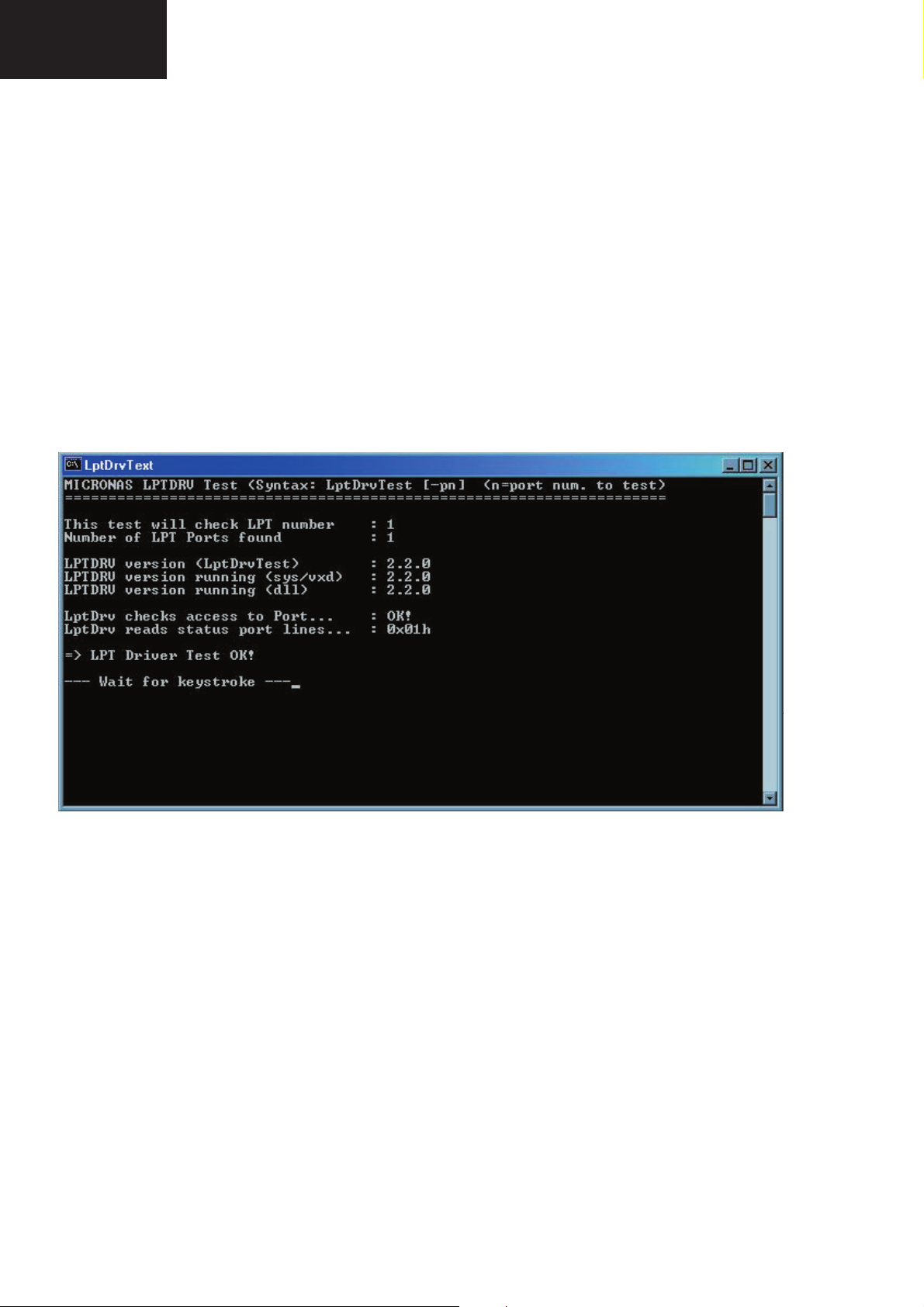
-Check installation of LPT driver:
C:\Program Files\Micronas\LptDrv\LptDrvTest.exe
If the LPT Driver is OK, the next picture shows:
If this test is not OK, check in your BIOS: Parallel Port Mode = EPP
Access to folder:
-D:\SOFTWARE UPDATE GA5\Installation order VCTi\VCT49xyi
-Copy all the content to the folder C:\Program Files\Micronas\Visual I2C and after selecting all fi les and directories
and change the «Read only» property. (When you copy from CD, the fi les are read only protected)
Check your installation:
-When you fi nish this process the Visual I2C is ready for Win2000 and XP
-LptDriver V.2.2.0 and VctiDown.exe V 1.3 are installed.
-If you have Win98 is necessary change version VctiDown.exe.
-Extract C:\Program Files\Micronas\Visual I2C\VCT49xyi\download\VctiDown_v1-2.zip in the same folder.
-Check LptDriver V1.4.0 and VctiDown.exe V1.2 are installed (Win98).
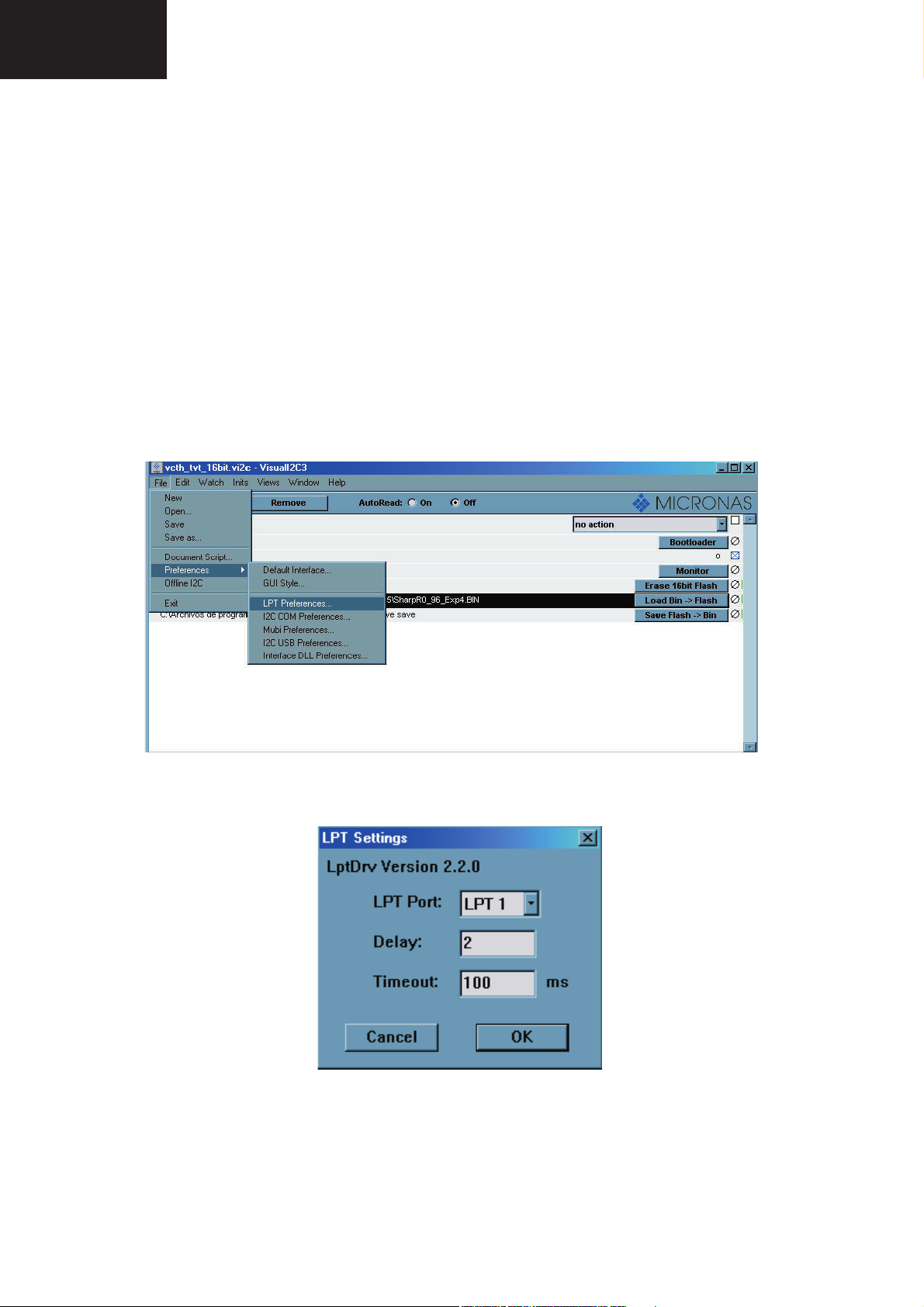
How to use the application
-To start VCTi software updater program, you can create direct access to:
C:\Program Files\Micronas\Visual I2C\VCT49xyi\vcth_tvt_16bit.vi2c
-Run direct access «vcth_tvt_16bit.vi2c».
30
Page 31

-Press OK and Error disappear. Now the program is available for use.
LC-26GA6E/LC-26BV6E
LC-26GA5E
LC-32GA6E/LC-32BV6E
LC-32GA5E
LC-37GA6E
- Double click the fi le name in the Load Bin fi eld and select the software version fi le.
- The fi rst time that you do this process, confi rm that the fi eld address is from 0x800000 to 0x8FFFFF.
31
Page 32
LC-26GA6E/LC-26BV6E
LC-26GA5E
LC-32GA6E/LC-32BV6E
LC-32GA5E
LC-37GA6E
- Enter the TV in Service Mode.
- Select OTHERS / FLASH UPGRADE.
- Change from OFF to ON.
- Switch OFF and Switch ON the TV.
Now the TV does not have watchdog and it is possible to make bootloader.
- Select Bootloader option. Set AutoRead to ON and wait until 22 appears in Bootlader Version fi eld.
- Click on the button Erase 16bit Flash. The bootloader version will be zero during few seconds. When the
version fi eld marks again 22 set Auto Read OFF.
- Click on the button LOAD BIN -> FLASH and the updating will start up.
- The updating will end before the progress bar reaches the end; if there is no error message the updating has
been good.
Sometime the progress bar is very quick or error message appears, then is necessary increase the delay until the
problem disappear:
-Select LPT Preference.
- Increase Delay: normally 2 or 3 are the best choice.
If there are further problems to enter the bootloader mode you can use the hardware method:
- Power off VCTi or hold RESET line to GND.
- Pull down SCL line to GND.
- Power up VCTi or release RESET line.
- Release SCL pull down after minimum of 1 second.
- Check if VCTi is in bootloader mode with a AutoRead.
32
Page 33
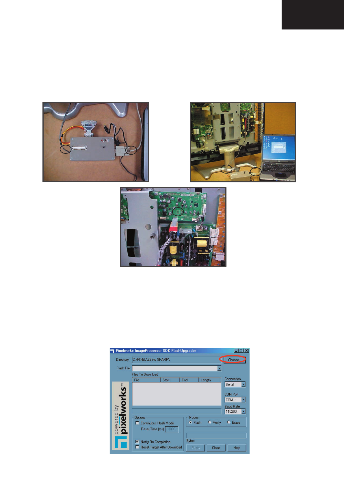
How to Update Pixelworks Software
Hardware requirements
To update Pixelworks it is needed:
1. A female DB9 to male DB9 wire and the updating tool (Part Code: CKIT-0002WJV0).
2. Make the connections as indicated below.
2.1. Connect a Serial cable from the updating tool to the PC.
2.2. Connect the long cable from the updating tool to the P2005 connector (LCD Controller PWB).
2.2
LC-26GA6E/LC-26BV6E
LC-26GA5E
LC-32GA6E/LC-32BV6E
LC-32GA5E
LC-37GA6E
2.2
2.1
2.2
2.1
2.2
Software requirements
Pixel Works FlashUpgrader.
Software preparation
- Create in the PC C:\Pixel folder.
- Copy fi le FlashUpgrader.exe from D:\SOFTWARE UPDATE GA5\Pixel Works to C:\Pixel that you have created
previously.
How to use the application
- Switch on the set you want to update and enter in service mode.
- Double click on C:\Pixel\FlashUpgrader.exe to start the program. The below picture appear:
33
Page 34

LC-26GA6E/LC-26BV6E
LC-26GA5E
LC-32GA6E/LC-32BV6E
LC-32GA5E
LC-37GA6E
- Click on «Choose» and select the QTV.inf fi le where you have the software version.
File
name
File
type
- Click on Flash button and the program is waiting for target reset.
Open
Cancel
- Press Input mode (TV/Video) key on the remote control to reset the Pixel IC and start updating.
If there is not reported any error the update is done, but you can verify the update following the same process but
selecting Verify mode.
34
Page 35

How to Update the Monitor Microcontroller Software
There are 2 ways to update the monitor microcontroller software:
1. Only LCD controller board itself
2. TV Set (already assembled)
Preparation
- (A) MoniWrite.exe(Application)
- (B) Monitor microcontroller software (*.MOT)
- (C) RS-232C cross cable
- (D) Serial controller board. (Part code: CKIT-0003WJV0).
LC-26GA6E/LC-26BV6E
LC-26GA5E
LC-32GA6E/LC-32BV6E
LC-32GA5E
LC-37GA6E
Connection
1. Only LCD controller board itself
1.1- Connect serial controller board (D) and PC with RS-232C cross cable (C).
1.2- Connect serial controller board (D) and the connector P2001 on LCD controller board.
1.3- Supply 6V to No.4 of P7707 on LCD controller board.
35
Page 36

LC-26GA6E/LC-26BV6E
LC-26GA5E
LC-32GA6E/LC-32BV6E
LC-32GA5E
LC-37GA6E
2. TV set
2.1- Connect serial controller board (D) and PC with RS-232C cross cable (C).
2.2- Connect serial controller board (D) and the connector P2005 on LCD controller board via adapter (E).
2.3- Plug AC cable.
Photo connection.
36
Page 37

How to use the application (MoniWrite.exe)
1. Start application
The following windows open.
LC-26GA6E/LC-26BV6E
LC-26GA5E
LC-32GA6E/LC-32BV6E
LC-32GA5E
LC-37GA6E
2. Select COM port
Select COM port connected with Serial Controller Board.
37
Page 38

LC-26GA6E/LC-26BV6E
LC-26GA5E
LC-32GA6E/LC-32BV6E
LC-32GA5E
LC-37GA6E
3. Select ResetLogic
Select ResetLogic «positive» or «negative».
Resetlogic setting for each level hardware
4. Open MOT File
4.1- Click «Open MOT File».
38
Page 39

4.2- Select the monitor microcontroller software (*.MOT) to update.
4.3- Check the selected fi le is correct.
LC-26GA6E/LC-26BV6E
LC-26GA5E
LC-32GA6E/LC-32BV6E
LC-32GA5E
LC-37GA6E
5. Send Start
5.1- Click «SendStart» button and start updating.
39
Page 40

LC-26GA6E/LC-26BV6E
LC-26GA5E
LC-32GA6E/LC-32BV6E
LC-32GA5E
LC-37GA6E
5.2- Now updating....
( Send fl ash writing control program fi rst, and then send the software.)
5.3- Update completed.
6. After update completed
6.1- Unplug AC cable
6.2- Disconnect serial control board.
40
Page 41

LC-26GA6E/LC-26BV6E
LC-26GA5E
LC-32GA6E/LC-32BV6E
LC-32GA5E
LC-37GA6E
TROUBLESHOOTING TABLE
Previously to start following the behing troubleshooting tables, consider the below situations.
Problem Possible Solution
• No power.
• Unit cannot be operated.
• Remote control unit does not operate.
• Strange colour, light colour, or dark,
or colour misalignment.
• Power is suddenly turned off.
• No picture.
• Is the AC cord disconnected?
• Has the power been turned on?
• Make sure the a (Power) switch of the TV is set to on.
• External influences such as lightning, static electricity, etc., may cause improper operation.
In this case, operate the unit after first turning the power off, or unplugging the AC cord
and re-plugging it in after 1 or 2 minutes.
• Are batteries inserted with polarity (e, f) aligned?
• Are batteries worn out? (Replace with new batteries.)
• Are you using it under strong or fluorescent lighting?
• Is a fluorescent light illuminated to remote control sensor?
• Adjust the picture levels.
• Is the room too bright? The picture may look dark in a room that is too bright.
• Check the system setting.
• Check the input type setting.
• The unit’s internal temperature has increased.
• Remove any objects blocking vent or clean.
• Check the power control setting.
• Is connection to other components correct?
• Has input type setup been done correctly after connection?
• Is the correct input selected?
• Is a non-compatible signal being input?
• Is picture adjustment correct?
• Is the antenna connected properly?
• No sound.
• Is the volume too low?
• Make sure that headphones are not connected.
• Make sure the sound is not set to Mute.
Cautions regarding use in high and low temperature environments
• When the unit is used in a low temperature space (e.g. room, office), the picture may leave trails or appear slightly delayed. This is
not a malfunction, and the unit will recover when the temperature returns to normal.
• Do not leave the unit in a hot or cold location. Also, do not leave the unit in a location exposed to direct sunlight or near a heater, as
this may cause the cabinet to deform and the LCD panel to malfunction.
Storage temperature: –20°C to +60°C (–4°F to +140°F).
41
Page 42

LC-26GA6E/LC-26BV6E
LC-26GA5E
LC-32GA6E/LC-32BV6E
LC-32GA5E
LC-37GA6E
Troubleshooting Table (continued)
No power supply (Front LED is off) and no power-up. (Front LED does not change from red to green)
Is the power supply cord properly connected to the Main unit?
<Power supply>
Are F701 and F702 normal?
Is F703 normal?
Is thermal fuse (F704) normal? (117°C specification)
Are the wire harness, FFC, etc. in the set connected properly?
Is a voltage of about 380 V applied to C709 and C710 when
power is turned on?
Is voltage generated at the +13V line (pin 1 of CN706)
immediately after supplying power?
YES
YES
YES
YES
YES
YES
YES
NO
NO
NO
NO
NO
NO
NO
Reconnect the power supply cord and turn on the power.
Replace F701 and F702, and then turn on the power. If a fuse
still blows, replace VA702, D701 and IC701, and then check again.
Replace F703 and then turn on the power. If a fuse still blows,
replace D763 and IC703, and then check again.
After replacing F704 and rechecking the mounting of D701,
D705, Q701, Q702, Q710 and Q711, supply power again. If the
fuse burns out again, replace the said parts and recheck.
Reconnect the wire harness, FFC, etc. and check again.
Check the 380V system power supply circuit. (L703, IC701,
Q701~5, D705, TH701)
Check the power supply circuit of the 13V system.
(T701, T702, F704, Q706-14, PC701, PC703-4, D708-17,
IC702, L710, Q733-6, D735-6, D771, IC706)
Is "H" signal sent to the PS_ON (pin 5 of CN707) line?
Is +3.3V line (pins 11/12 of CN706) normal immediately after
supplying power?
Is F1001 (2.5A) of the Main PWB normal?
YES
Is each REG-IC output normal?
(IC708 (4V), IC740 (33V), IC709 (5V), IC713 (12V), Q760 (6V))
NO
NO
Check the power supply circuit of the +3.3V line system.
(IC715, L715, T703, IC703, PC701-702) (F1001)
Check each REG-IC and each line.
42
Page 43

NO
NO
NO
NO
NO
NO
YES
YES
YES
YES
YES
YES
No audio output (1) (On the reception of TV broadcasting)
No audio output on the reception of
UHF/VHF.
Confirmation of the settings:
1) Is volume of REMOCON set to MIN or MUTE? … Set to any value.
2) Are headphones connected to HEADPHONE (J402)? … Disconnect.
3) Is ANT-CABLE disconnected or is there a connection error? … Connect according to the operation manual.
4) Is "VOLUME" in MENU-SOUND-LEVELS-SPEAKERS-VOLUME set to "MIN=0"? … Set to the desired value between "0-100".
Are audio signals (SPL/R) sent from the
pins (123)(124) of IC1001 (VCTI)?
Are audio signals of the pins (1)(7) of
IC1351 sent normally?
Are audio input signals of the pins (11)(15)
of IC1301 (AUDIO-AMP-IC) normal?
Are audio output signals of the pins
(28)(31)/(24)(27) of IC1301 (AUDIO-AMP-
IC) normal?
Check the connector (P1301) and the left
and right SP-boxes.
Check IC1351 or its peripheral
circuits.
Check the HEADPHONE JACK
(J402) or its peripheral circuits.
Check IC1301 and its peripheral
circuits.
Are IF signals (IF+/IF-) sent to the pins
(109)(110) of IC1001 (VCTI)?
Is IF signal sent from the pin (11) of
TUNER (TU1201)?
Check if power of 33V/5V is supplied to
the pins (9)/(7) of TUNER (TU1201). Or
check its peripheral parts.
Check if +8V, +5V and +3.3V are supplied
to the pins (126), (106) and (105) of
IC1001respectively. Or check its
peripheral circuits.
Check SF1201 and its peripheral circuits.
Troubleshooting Table (continued)
LC-26GA6E/LC-26BV6E
LC-26GA5E
LC-32GA6E/LC-32BV6E
LC-32GA5E
LC-37GA6E
43
Page 44

LC-26GA6E/LC-26BV6E
LC-26GA5E
LC-32GA6E/LC-32BV6E
LC-32GA5E
LC-37GA6E
Troubleshooting Table (continued)
No audio output (2) (On the reception of TV broadcasting, audio from the EXT.
terminal to the external device)
No audio output from EXT1 Terminal.
Is output (A-OUT-L/R) of Pins
(122)(121) of IC1001 (VCTI) normal?
YES
Are the signals (A-OUT-L/R) between
pins (122)(121) of IC1001 and pins
(1)(3) of SCART1 (SC1451) normal?.
YES
Check Q1011, Q1004 and Q1005 of the
2S-Mute circuit and 2S-MUTE-LINE.
No audio output from EXT2 and EXT3
Terminals.
Is output (A-OUT-L/R) of Pins
(120)(119) of IC1001 (VCTI) normal?
YES
Are the signals between pins (120)(119)
of IC1001 and pins (1)(3) of SCART2
(SC1452) normal?. Are the signals
between pins (120)(119) of IC1001 and
pins (5)(8) of SCART3 (J401) normal?.
IC1402
YES
Check (Q1012, Q1406, Q1408) and
(Q1013, Q1403, Q1404) of the S-Mute
circuit.
44
Page 45

YES
YES
YES
YES
NO
NO
NO
NO
NO
NO
NO
NO
NO
No audio output (3) (Output to external terminals)
No audio output from the
headphones.
No audio output from the
SCART1. (EXT-1)
No audio output from the
SCART2. (EXT-2)
No audio output from the
EXT-3.
Are audio signals sent to
the pins (5)(2) of the
headphone terminal
(J402)?
Are audio input/output
signals of the pins
(1)(7)/(3)(5) of IC1351
(HP-AMP) normal?
Are audio output signals
(SPL/R) sent to the pins
(123)(124) of IC1001
(VCTI) normally?
Check the audio input
signals of IC1001 (VCTI),
power supply line, I2C line,
and peripheral circuits.
Confirmation of the settings:
1) Is the MUTE button of REMOCON set to ON? … Set to OFF.
2) Is MENU-SOUND-LEVELS-EXTERNAL-SCART/AV VOL set to "0=MIN"? … Set the desired volume between "0-100".
3) Check the connection with external equipment. … Is there a connection error?
Are audio signals sent to
the pins (1)(3) of SCART-1
(SC1451)?
Are audio signals sent to
the pins (122)(121) of
IC1001?
Are audio signals sent to
the pins (1)(3) of SCART-2
(SC1452)?
Are audio signals sent to
the pins (1)(7) of IC1402?
Are audio L/R signals sent
to the pins (120)(129) of
IC1001?
Check the 2S-MUTE
and SS-MUTES
signals and peripheral
circuits.
Check IC1001 and its
peripheral circuits.
Check IC1001 and its
peripheral circuits.
Check IC1402 and its
peripheral circuits.
Are audio signals sent to
the pins (5)(8) of the EXT
-
3 external terminal J401?
Troubleshooting Table (continued)
LC-26GA6E/LC-26BV6E
LC-26GA5E
LC-32GA6E/LC-32BV6E
LC-32GA5E
LC-37GA6E
45
Page 46
LC-26GA6E/LC-26BV6E
A
(3)(13)
A
(
p
A
(1)(7)
A
A
A
g
p
p
LC-26GA5E
LC-32GA6E/LC-32BV6E
LC-32GA5E
LC-37GA6E
Troubleshooting Table (continued)
No audio output (4) (Sound from external input terminals)
External audio input signals
supplied from SCART1 and EXT3
are not heard.
<SCART1>
Is LI1 audio signal supplied from
the pin (6) of the input terminal
SC1451 to the pin (114) of
IC1001?
Is RI1 audio signal supplied from
the pin (2) of the input terminal
SC1451 to the pin (113) of
IC1001?
<EXT3>
Is LI2 audio signal supplied from
the J401 terminal to the pin (116)
of IC1001?
Is RI2 audio signal supplied from
the J401 terminal to the pin (115)
of IC1001?
YES YES
External audio input signals
supplied from SCART2 and PC
INPUT are not heard.
<SCART2>
Is L audio signal supplied from
the pin (6) of the input terminal
SC1452 to the pin (15) of
IC1401?
Is R audio signal supplied from
the pin (2) of the input terminal
SC1452 to the pin (2) of IC1401?
<PC-INPUT>
Is L audio signal supplied from
the PC-AUDIO CONNECTOR
(J402) to the pin (12) of
IC1401?
Is R audio signal supplied from
the J402 CONNECTOR to the
pin (1) of IC1401?
re audio signals sent to the pins
of IC1401?
NO
Check IC1401 and its
eripheral circuits.
YES
re LI3 and RI3 audio signals
supplied to the pins (118) and
117) of IC1001 respectively?
YES
re audio signals sent to the pins
of IC1351 normally?
YES
re audio input signals of the
pins (11) (15) of IC1301(AUDIO-
MP-IC) normal?
YES
re audio output signals of the
pins (28)(31)/(24) (27) of
-
-
YES
Check the connector (P1301)
and the left and ri
ht SP-boxes.
Check IC1351 and its
NO
eripheral circuits.
NO
Check HEADPHONEJACK (J402) or its
NO
Check IC1301 and its
eripheral circuits.
46
Page 47
Troubleshooting Table (continued)
LC-26GA6E/LC-26BV6E
LC-26GA5E
LC-32GA6E/LC-32BV6E
LC-32GA5E
LC-37GA6E
YES
No audio output (5)
YES
YES
Is the output analogue signal of NO Check IC1906 and
11 of IC1905 as specified? peripheral components
pins 1 and 3 of P2103 ? peripheral components
YES
Is the output signal pin 9 and 7 of NO Check Components
P2101 as specified? units and peripheral.
Are audio signals sent to the pins NO Check IC1351 and its
(1) (7) of IC1351 normally? peripheral circuits.
YES
(11) (15) of IC1301(AUDIO-AMP-IC) JACK (J402) or its
Are audio input signals of the pins NO Check HEADPHONE-
YES
normal? peripheral circuits.
Are audio output signals of the NO Check IC1301 and its
pins (28)(31)/(24) (27) of IC1301 peripheral circuits.
YES
(AUDIO-AMP-IC) normal?
the left and right SP-boxes.
Check the connector (P1301) and
No external input sound Ex 4 comes out No external analogue input sound Ex 5 comes out No external digital input sound Ex 5 comes out
Is the inputted signal from J1901 to NO Check IC1906 and Is the inputted signal from J1902 to NO Check IC1906 and Is the output digital signal pins 84, 85 and NO Check IC1904 and
input terminals 1 and 3 of P2103 ? peripheral components input terminals 1 and 3 of P2103 ? peripheral components 86 of IC1904 as specified? peripheral components
YES YES Is the output analogue signal pins 10 and NO Check IC1905 and
47
Page 48
LC-26GA6E/LC-26BV6E
LC-26GA5E
LC-32GA6E/LC-32BV6E
LC-32GA5E
LC-37GA6E
Troubleshooting Table (continued)
YES
Is FM-IF signal sent from the pin (4) of
peripheral circuits.
Check if +8V, +5V and +3.3V are
supplied to the pins (126), (106) and
(105) of IC1001 respectively. Or check its
IC1201 (MIXER
Check SF1201 and its peripheral
circuits.
No audio output ()
YES
Are IF signals (IF+/IF-) supplied to the
pins (109)(110) of IC1001 (VCTI)?
YES
NO
NO
Is FM-IF signal sent from the pin (10)
of TUNER (TU1201)?
Check IC1351 or its peripheral
circuits.
Check if power of 33V/5V is supplied
Check HEADPHONE-JACK
to the pins (9)/(7) of TUNER
(TU1201). Or check its peripheral
parts.
(J402) or its peripheral circuits.
Check IC1301 and its peripheral
circuits.
No FM sound.
NO
YES
Confirmation of the settings:
1) Is the MUTE button of REMOCON set to ON? … Set to OFF.
2) Are headphones connected to HEADPHONE (J402)? … Disconnect.
3) Is FM-ANT-CABLE disconnected or is there a connection error? … Connect according to the operation manual.
4) Is "VOLUME" in MENU-SOUND-LEVELS-SPEAKERS-VOLUME set to "MIN=0"? … Set to the desired value between "0-100".
Are audio signals (SP L/R) sent from
the pins (123)(124) of IC1001 (VCTI)?
48
NO
Are audio output signals of the pins
(1)(7) of IC1351 (H-PHONE-AMP)
normal?
NO
YES
Are audio input signals of the pins
YES
(11)(15) of IC1301 (AUDIO-AMP-IC)
normal?
NO
YES
Check the connector (P1301) and the
Are audio output signals of the pins
(28)(31)/(24)(27) of IC1301 (AUDIO-
AMP-IC) normal?
left and right SP-boxes.
Page 49

Troubleshooting Table (continued)
LC-26GA6E/LC-26BV6E
LC-26GA5E
LC-32GA6E/LC-32BV6E
LC-32GA5E
LC-37GA6E
<On input of the tuner (U/V)> No picture (1)
No picture appears on the reception of the tuner (U/V)
Confirmation of the settings:
1) Is "INPUT MODE" of remote control set properly?.... Set "INPUT MODE" to TV referring to the operation manual.
2) Is MENU-PICTURE-LEVELS-CONTRAST/BRIGHTNESS set to "MIN"?... Set to the desired level.
3) Is ANT-CABLE disconnected or is there a connector error?....Connect according to the operation manual.
YES
Is video signal (IF) sent from the pin NO Check the tuner (TU1201) and its
(11) of TUNER(TU1201)? peripheral circuit
YES
Are video signals sent from the pins NO Check the SF1201 and its peripheral
(4) and (5) of SF1201 (SAW FIL) ? circuits
YES
YES NO
Are video signals (IF± ) supplier to NO Check SF1201 to the pins (109) (110) of
the pins (109)(110) IC1001 (VCTI)? IC1001 (VCTI) and peripheral circuits
YES NO
Are digital video output (ITU 656 71 ~ 80) and synchro signals (81, 82) of IC 1001? Check IC1001, IC1002, IC 1003 and peripheral components.
Are R,G,B and synchro output signals at pins (97, 94,91, 34 and 35 ) as specified? Check IC6004and peripheral components
YES YES
Are R,G,B output signals at pins NO Check IC1001 and peripheral Are synchro signal at pins (34) NO Check IC1001, IC 6004 and
(1) (144) and (143) of IC1001 as specified? components (35 ) of IC 6004 as specified? peripheral components
YES YES
Are R,G,B input signals at pins NO Check Q1802, Q1803, Q1804 Are synchro input signals at pins NO Check IC 2205 and IC 1803 and
49
(2) (5) (14) of IC1801 as specified? and peripheral components (4) (13) of IC 2206 as specified? peripheral components
YES YES
Are R,G,B input signals at pins NO Check IC1801, IC1802 Are synchro input signals at pins NO Check IC 2206 and peripheral
(14) (5) (11) of IC 2203 as specifeid? and peripheral components (64) (65) of IC 2201 as specified? components
YES
Are R,G,B input signals at pins NO Check IC2203 and IC1803
(37) (43) (50) of IC2201 as specified? and peripheral components YES
YES
YES
and (DVS 101) (DHS 102) (DEN 103) (DCLOK 106) of IC2201 as specified? peripheral components
Are video digital output signals at pins (DEB 66 ~ 78) ( DEG 79 ~ 88) ( DER 89 ~ 98) (DOB 98 ~ 113) (DOG 114 ~ 121) (DOR 124 ~ 131) NO Check IC 2201, IC 2210 and
YES
Are digital video signals (TA2 ± ~ TD2 ± ) sent to the pins (18) ~ (31) of LV connector (SC2201) ? components
Are digital video signals (TA1± ~ TD1± ) sent to the pins (3) ~ (16) of LV connector (SC2201) on MAIN PWB? NO Check IC 2207 and peripheral
Check the LCD CONTROLLER Unit
Page 50
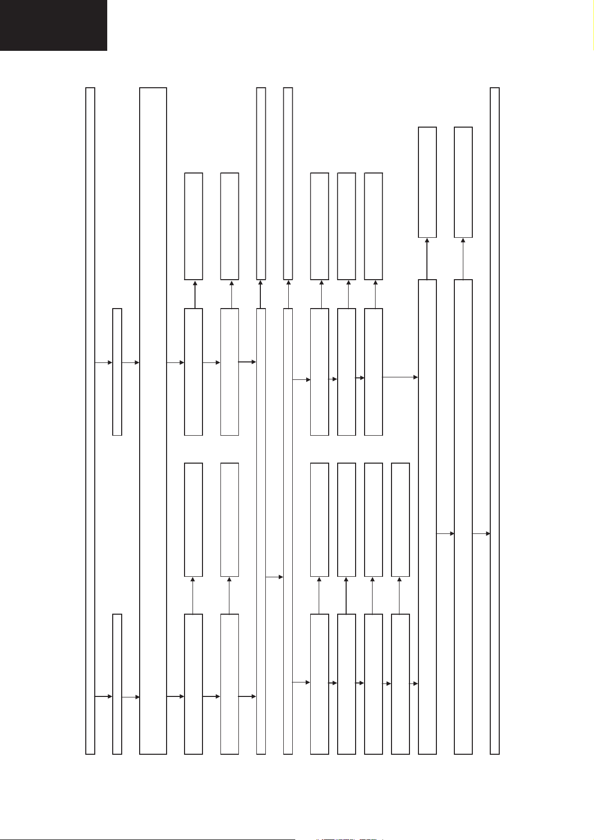
LC-26GA6E/LC-26BV6E
t
LC-26GA5E
LC-32GA6E/LC-32BV6E
LC-32GA5E
LC-37GA6E
Troubleshooting Table (continued)
NO Check SC 1451 connector and
YES
YES NO
< When external connected > No picture (2)
External input in trouble <EXT-1> External input R,G,B in trouble <EXT-1>
YES YES
Confirmation of the settings:
1) Is "INPUT MODE" of remote control set properly?.... Set "INPUT MODE" to EXT.1 referring to the operation manual.
2) Is MENU-PICTURE-LEVELS-CONTRAST/BRIGHTNESS set to "MIN"?... Set to the desired level.
YES YES
Is video signal sent to the pin (19) of NO Check the connection with external Is there R,G and B at pins 5 , 2 and 12 a
scart 1? equipment or input setting IC1403 as specified ? peripherical components.
YES YES
Is there video signal input at pin (66) NO Check SC1451 and peripherical Is there R, G and B signal input at pins NO Check IC 1403, Q 1412 and
of IC 1001 ? components 67, 68 and 69 of IC 1001 as specified ? peripherical components
YES YES NO
Are digital video output (ITU 656 71 ~ 80) and synchro signals (81, 82) of IC 1001? Check IC1001, IC1002, IC 1003 and peripheral components.
Are R,G,B and synchro output signals at pins (97, 94,91, 34 and 35 ) as specified? Check IC6004and peripheral components
YES YES
Are R,G,B output signals at pins NO Check IC1001 and peripheral Are synchro signal at pins (34) NO Check IC1001, IC 6004 and
(1) (144) and (143) of IC1001 as specified? components (35 ) of IC 6004 as specified? peripheral components
YES YES
Are R,G,B input signals at pins NO Check Q1802, Q1803, Q1804 Are synchro input signals at pins NO Check IC 2205 and IC 1803 and
(2) (5) (14) of IC1801 as specified? and peripheral components (4) (13) of IC 2206 as specified? peripheral components
YES YES
Are R,G,B input signals at pins NO Check Q1801, Q1802 Are synchro input signals at pins NO Check IC 2206 and peripheral
(4) (5) (11) of IC 2203 as specified? and peripheral components (64) (65) of IC 2201 as specified? components
YES
Are R,G,B input signals at pins NO Check IC2203 and IC1803
and (DVS 101) (DHS 102) (DEN 103) (DCLOK 106) of IC2201 as specified? peripheral components
(37) (43) (50) of IC2201 as specified? and peripheral components YES
YES
Are video digital output signals at pins (DEB 66 ~ 78) ( DEG 79 ~ 88) ( DER 89 ~ 98) (DOB 98 ~ 113) (DOG 114 ~ 121) (DOR 124 ~ 131) NO Check IC 2201, IC 2210 and
YES
Are digital video signals (TA1± ~ TD1± ) sent to the pins (3) ~ (16) of LV connector (SC2201) on MAIN PWB? NO Check IC 2207 and peripheral
Are digital video signals (TA2 ± ~ TD2 ± ) sent to the pins (18) ~ (31) of LV connector (SC2201) ? components
Check the LCD CONTROLLER Unit
50
Page 51

Troubleshooting Table (continued)
LC-26GA6E/LC-26BV6E
LC-26GA5E
LC-32GA6E/LC-32BV6E
LC-32GA5E
LC-37GA6E
on screen ?
YES NO
YES
YES
< When external connected > No picture (3)
External input in trouble <EXT-2> External input S-VIDEO in trouble <EXT-2>
YES YES
Confirmation of the settings:
1) Is "INPUT MODE" of remote control set properly?.... Set "INPUT MODE" to EXT.2 or S-VIDEO referring to the operation manual.
2) Is MENU-PICTURE-LEVELS-CONTRAST/BRIGHTNESS set to "MIN"?... Set to the desired level.
YES YES
Is video signal sent to the pin (19) of NO Check the connection with external
scart 2? equipment or input setting NO Is there luminance
YES YES
Is there video signal input at pin (64) NO Check SC1452 and peripherical Is chroma signal input NO Check SC 1452 and
of IC 1001 ? components at pin (65) of IC 1001? peripherical components
YES YES NO
Are digital video output (ITU 656 71 ~ 80) and synchro signals (81, 82) of IC 1001? Check IC1001, IC1002, IC 1003 and peripheral components.
Are R,G,B and synchro output signals at pins (97, 94,91, 34 and 35 ) as specified? Check IC6004and peripheral components
YES YES
Are R,G,B output signals at pins (1) NO Check IC1001 and peripheral Are synchro signal at pins (34) NO Check IC1001, IC 6004 and
(144) and (143) of IC1001 as specified? components (35 ) of IC 6004 as specified? peripheral components
YES YES
YES YES
Are R,G,B input signals at pins NO Check Q1802, Q1803, Q1804 Are synchro input signals at pins NO Check IC 2205 and IC 1803 and
(2) (5) (14) of IC1801 as specified? and peripheral components (4) (13) of IC 2206 as specified? peripheral components
51
Are R,G,B input signals at pins NO Check Q1801, Q1802 Are synchro input signals at pins NO Check IC 2206 and peripheral
(4) (5) (11) of IC 2203 as specified? and peripheral components (64) (65) of IC 2201 as specified? components
YES
Are R,G,B input signals at pins NO Check IC2203 and IC1803
(37) (43) (50) of IC2201 as specified? and peripheral components YES
YES
Are video digital output signals at pins (DEB 66 ~ 78) ( DEG 79 ~ 88) ( DER 89 ~ 98) (DOB 98 ~ 113) (DOG 114 ~ 121) (DOR 124 ~ 131) NO Check IC 2201, IC 2210 and
and (DVS 101) (DHS 102) (DEN 103) (DCLOK 106) of IC2201 as specified? peripheral components
Are digital video signals (TA1± ~ TD1± ) sent to the pins (3) ~ (16) of LV connector (SC2201) on MAIN PWB? NO Check IC 2207 and peripheral
Are digital video signals (TA2 ± ~ TD2 ± ) sent to the pins (18) ~ (31) of LV connector (SC2201) ? components
Check the LCD CONTROLLER Unit
Page 52

LC-26GA6E/LC-26BV6E
LC-26GA5E
LC-32GA6E/LC-32BV6E
LC-32GA5E
LC-37GA6E
Troubleshooting Table (continued)
on screen ?
YES NO
YES
YES
< When external connected > No picture (4)
External input in trouble <EXT-3> External input S-VIDEO in trouble <EXT-3>
YES YES
Confirmation of the settings:
1) Is "INPUT MODE" of remote control set properly?.... Set "INPUT MODE" to EXT.3 or S-VIDEO referring to the operation manual.
2) Is MENU-PICTURE-LEVELS-CONTRAST/BRIGHTNESS set to "MIN"?... Set to the desired level.
YES YES
Is video signal sent to the pin (19) of NO Check the connection with external
video 3? equipment or input setting NO Is there luminance
of IC 1001 ? components at pin (63) of IC 1001? peripherical components
YES YES
Is there video signal input at pin (60) NO Check J 401 and peripherical Is chroma signal input NO Check J 403 and
(37) (43) (50) of IC2201 as specified? and peripheral components YES
YES
(4) (5) (11) of IC 2203 as specified? and peripheral components (64) (65) of IC 2201 as specified? components
(2) (5) (14) of IC1801 as specified? and peripheral components (4) (13) of IC 2206 as specified? peripheral components
YES YES
YES YES NO
Are digital video output (ITU 656 71 ~ 80) and synchro signals (81, 82) of IC 1001? Check IC1001, IC1002, IC 1003 and peripheral components.
Are R,G,B and synchro output signals at pins (97, 94,91, 34 and 35 ) as specified? Check IC6004and peripheral components
YES YES
Are R,G,B input signals at pins NO Check Q1802, Q1803, Q1804 Are synchro input signals at pins NO Check IC 2205 and IC 1803 and
(1) (144) and (143) of IC1001 as specified? components (35 ) of IC 6004 as specified? peripheral components
Are R,G,B output signals at pins NO Check IC1001 and peripheral Are synchro signal at pins (34) NO Check IC1001, IC 6004 and
YES
YES YES
Are R,G,B input signals at pins NO Check Q1801, Q1802 Are synchro input signals at pins NO Check IC 2206 and peripheral
Are video digital output signals at pins (DEB 66 ~ 78) ( DEG 79 ~ 88) ( DER 89 ~ 98) (DOB 98 ~ 113) (DOG 114 ~ 121) (DOR 124 ~ 131) NO Check IC 2201, IC 2210 and
Are R,G,B input signals at pins NO Check IC2203 and IC1803
52
and (DVS 101) (DHS 102) (DEN 103) (DCLOK 106) of IC2201 as specified? peripheral components
Are digital video signals (TA1± ~ TD1± ) sent to the pins (3) ~ (16) of LV connector (SC2201) on MAIN PWB? NO Check IC 2207 and peripheral
Are digital video signals (TA2 ± ~ TD2 ± ) sent to the pins (18) ~ (31) of LV connector (SC2201) ? components
Check the LCD CONTROLLER Unit
Page 53

Troubleshooting Table (continued)
LC-26GA6E/LC-26BV6E
LC-26GA5E
LC-32GA6E/LC-32BV6E
LC-32GA5E
LC-37GA6E
No video output (5)
External input in trouble <EXT 4> External input in trouble <EXT 4>
Components SD Components HD
YES YES
YES YES
YES YES
YES
Is there Y, Pr and Pb signal output at pins NO Check IC 1801, IC 1802 and
12 , 4 and 7 of IC1801 as specifed ? peripherical components
YES
YES YES
YES YES
Is there Y, Pr and Pb signal output at pins NO Check IC 2203 , IC 1803 and
12 , 9 and 7 of IC2203 (RGB-SW) as specified ? peripherical components
Is there Y, Pr and Pb signal input at pins NO Check IC 2201 and
37, 43 and 50 of IC2201 (SCALER) as specified ? peripherical components
<Signals>
Confirmation of the settings:
1) Is "INPUT MODE" of remote control set properly?.... Set "INPUT MODE" to EXT.4 referring to the operation manual.
2) Is MENU-CONTRAST/BRIGHTNESS set to "MIN"?... Set to the desired level.
Select EXT 4 and the input signal NO Is EXT 4 selected in the input Is EXT 4 selected in the input NO Select EXT 4 in the
in the input switching menu screen switching menu screen ? switching menu screen ? input switching menu screen
Select SD in main menu AV set-up NO Is SD select in Main menu? Is HD select in Main menu? NO Select HD in main menu AV set-up
Ext 4 SD Ext 4 HD
Check IC2001 and NO Is there Y, Pr and Pb signal outputs at pins Is there Y, Pr and Pb signal outputs at pins NO Check IC2001 and
peripherical components 3, 5 and 6 of IC 2101 as specified ? 3, 5 and 6 of IC 2101 as specified ? peripherical components
Check Q2101, 2102, 2103, 2104, 2105 NO Is there Y, Pr and Pb signal at pins 2, 4 and 6 Is there Y, Pr and Pb signal at pins 1, 3 and NO Check Q2101, 2107, 2108
and 2106 and peripherical components of P2102 as specified ? 5 of P2101 as specified ? 2109 and peripherical components
Check IC 1403, Q 1412 and NO Is there Y, Pr and Pb signal input at pins Is there Y, Pr and Pb signal input at pins NO Check Components unit PWB and
peripherical components 67, 68 and 69 of IC 1001 as specifed ? 13, 6 and 3 of IC 1801 as specifed ? peripherical components
53
Page 54

LC-26GA6E/LC-26BV6E
/
LC-26GA5E
LC-32GA6E/LC-32BV6E
LC-32GA5E
LC-37GA6E
Troubleshooting Table (continued)
<On HDMI input> No picture (6)
No EXT5-MDMI signal during external input
Checklist:
1) Is "INPUT MODE" button on the remote control set up correctly?..........See the operation manual and set "INPUT MODE" to EXT5".
2) Is MENU CONTRAST/BRIGHTNESS set to "MIN"?........................................Set it to an appropriate level.
3) Is CABLE disconnected, or incorrectly connected?.......................................Connect it correctly as per the operation manual.
NO
COMPONENT-UNIT
Are Y, Pb and Pr signals sent from pins Are HDMI-Y, Pb and Pr signals Check IC2101 or
(6), (5) and (3) of IC2101 (A-SW)? sent from pins (9), (14) and (1) peripheral circuits
YES NO
Check P2205/P2101 NO MAIN-UNIT: HDMI-UNIT:
CONNECTOR, Q2107_9 Are Y, Pb and Pr signals Is HDMI-Y/ Pb/Pr signal sent to between COMPONENT-UNIT
and peripheral circuits. sent to pins (6), (3) and pins (17, (14) and (20) of IC1904? HDMI-UNIT Check P2103/P1901
(13) of IC1801? and peripheral circuits.
YES NO
Check IC2203, IC1803 NO Are Y, Pb and Pr signals HDMI-UNIT:
and peripheral circuits. sent to pins (12), (9) and Is LVDS signal sent to pins (71-58) Check IC1904 or peripheral
(7) of IC2203? of IC1904? circuits.
YES NO
Check IC2201 and NO Are Y, Pb and Pr signals HDMI-UNIT:
peripheral circuits sent to pins (43), (50) and Is LVDS signal sent to pins (71-58) Check HDMI-Terminal SC1901
(37) of IC2201? (SCALER) of HDMI-Terminal SC1901? or peripheral circuits.
YES NO
Are video digital ouput signals ( DOR 124 - 131 ), ( DOG 114 - 121 ), ( DOB 99 - 113 ), ( DER 89 - 98 ),
( DEG 79 - 88 ) and ( DEB 66 - 78 ) of IC2201 (SCALER) sent properly? (F MEMORY) and peripheral
YES
COMPONENT-UNIT:
NO
of IC2101 (A-SW)?
Check HDMI-Terminal and
external connection
COMPONENT-UNIT:
YES
CONNECTOR
YES
YES
HDMI-UNIT:
HDMI-UNIT:
YES
Check IC2201 (LVDS), IC2210
NO
circuits.
Are digital video signals (TA1± ~ TD1± ) and (TA2 ± ~ TD2 ± ) sent to pins (3) - (16) and (18) - (31) of
MAIN PWB-LV connector SC2201 respectively? circuits.
YES
Check LCD-CONT-UNIT.
Check IC2207 and peripheral
NO
54
Page 55

Troubleshooting Table (continued)
LC-26GA6E/LC-26BV6E
LC-32GA6E/LC-32BV6E
LC-37GA6E
Check external
connection or input
setting.
Check the power
LC-26GA5E
LC-32GA5E
line of IC1001 and
peripheral circuits.
External input in trouble <PC INPUT>
Is "Ext. Sources menu " NO Set "Ext Sources menu " to PC INPUT
set properly ? referring to the operation manual
No video output (7)
YES YES
From EXT1/EXT2:
No picture appears on EXT3-connected
monitor.
Are R,G,B signal input at pins NO Check IC 2201 and peripheral
(37) (43) and (50) of IC 2201 ? components
8)
No picture (
YES
Is VIDEO signal
sent to pin (2) of
Check external
connection or input
YES
EXT3?
setting.
YES
Is VIDEO signal
Check the power
YES
NO
(FRONTAV) sent
to pin (60) of
IC1001?
Check that VIDEO
line of IC1001 and
peripheral circuits.
signal is sent to
pin (3) of EXT3.
YES
components pins (1) and (13) of IC 2205 NO
Check SC 2801 and peripheral NO Are there synchro signal input at Is there video on screen ?
YES YES
Check IC 2205 , IC1803 and NO Are synchro signal output at Are R,G,B signal input at pins NO Check SC 2801 and peripheral
peripheral components pins (14) and (15) of IC 2205? (6) (10) and (13) of IC 2203 ? components
YES (7) (12) and (9) of IC 2203 ? peripheral components
Check IC 2206 and peripheral NO Are synchro signal output at
components pins (6) and (11) of IC 2206? Are R,G,B signal output at pins NO Check IC 2203 , IC1803 and
From EXT1:
During TUNER reception:
Check IC 2201 and peripheral NO Are there synchro signal input at YES
components pins (64) and (65) of IC 2201 ?
<During external connection>
55
No picture appears on EXT2-connected
monitor.
Checklist:
1) Are input terminal on back of TV and "INPUT MODE" button on the remote control set up correctly?........See the operation manual and set
No picture appears on EXT1-connected
monitor.
"INPUT MODE" appropriately.
2) Is the specified device selected for Signal Type (item) in MENU-SETUP-AV SETUP-EXT?...............................Set it to "VCR or DVD or AUTO".
Is VIDEO signal
sent to pin (19) of
SCART2?
Check external
connection or input
setting.
YES
NO NO NO
Is VIDEO signal
sent to pin (19) of
SCART1?
Is VIDEO signal
(VIN2) sent to pin
(64) of IC1001?
Check the power
line of IC1001 and
peripheral circuits.
YES
NO NO
Is VIDEO signal
(VIN1) sent to pin
(66) of IC1001?
Check that VIDEO
signal is sent to
pin (20) of
SCART2.
Check that VIDEO
signal is sent to
pin (20) of
SCART1.
Page 56

LC-26GA6E/LC-26BV6E
The backlight does not go on.
NO
YES
NO
NO
YES
NO YES
YES
Inside the power supply unit: Has the fuse
F705 1A on the inverter circuit burnt out?
Is power supplied to the INVERTER PWB?
(Vin, 3.5VAC)
Are PWBs properly connected with
harnesses?
(Power supply unit, INVERTER PWB,
INVERTER-GND PWB, LCD
CONTROLLER PWB)
Connect properly or replace harnesses.
Check the inverter circuit behind the burnt
fuse.
Inside the power supply unit: Is each
control signal sent to CN704? (Pin (11) of
OFL1, pin (13) of INV.OSC)
Check the connectors of each fluorescent
lamp and inverter circuit.
Check IC4501 (LCD CONTROL) and its
peripheral circuits.
LC-26GA5E
LC-32GA6E/LC-32BV6E
LC-32GA5E
LC-37GA6E
Troubleshooting Table (continued)
56
Page 57

Troubleshooting Table (continued)
No picture in the LCD section
Is the power supplied to the LCD CONTROLLER PWB? (P7707: +6/+4/+13V)
Check if the REG output -D3.3V_1/2 of IC7706/IC7704 (REG-IC) is sent properly.
YES
Is the output signal of IC4601 (GAMMA) sent properly?
YES
Adjustment process menu: Is the gradation pattern displayed
properly when setting "PATTERN1" in the second llayer of
"LCD CONT" to "02"?
YES
Check IC4901 (QS-DRIVER) and its peripheral circuits.
Data bit drop (gradation-related)
NO
NO
LC-26GA6E/LC-26BV6E
LC-26GA5E
LC-32GA6E/LC-32BV6E
LC-32GA5E
LC-37GA6E
Check the FFC (LV, SC2201 - SC4601) between MAIN
PWB and LCD CONTROLLER PWB and input circuit of
IC4601.
Check IC4501 (LCD CONTROL) and its peripheral circuits.
Adjustment process menu: Is the gradation pattern displayed
properly when setting "PATTERN1" in the second layer of
"LCD CONT" to "02"?
YES
Adjustment process menu: Is the gradation pattern displayed
properly when setting "PATTERN2" in the second layer of
"LCD CONT" to "1"?
YES
Check IC4601 (GAMMA) and its peripheral circuits.
Noise is caused to the moving picture with the QS drive on.
Is the input voltage at pin (62) (OS-TEMP) of IC2004
(microprocessor) 5V?
YES
Is the harness connected correctly between the inverter GND
PWB and LCD CONTROLLER PWB?
YES
The thermistor on the INVERTER GND PWB is faulty. Or
check the peripheral circuits.
NO
NO
NO
NO
Check the connection between SC4651 and SC4652 and
peripheral circuits of IC4501 (LCD CONTROL).
Check IC4902 (FIFO) and its peripheral circuits.
Check IC4901 (QS-DRIVER) and its peripheral circuits.
Connect the harness correctly or replace it.
The whole screen is whitish (LCD power supply).
Adjustment process menu: Is the gradation pattern displayed
properly when setting "PATTERN2" in the second layer of
"LCD CONT" to "1"? (Is it whitish or dark?)
NO
Disconnect the FPC from SC4651 and SC4652. (To protect
the panel against damage)
YES
Check the power supply voltage supplied to the panel (check
at SC4651 and SC4652).
YES
Check the video signal circuits (IC4501, IC4901, IC4601).
57
Page 58

LC-26GA6E/LC-26BV6E
LC-26GA5E
LC-32GA6E/LC-32BV6E
LC-32GA5E
LC-37GA6E
Main Unit Layout QPWBXD334WJN2
IC2801
SC2801
I
CHASSIS LAYOUT
P2205
P2206
SC2201
IC2202
IC1801
IC2201
X2201
IC2210
H
IC6008
IC1002
IC2207
IC2211
IC1006
P2203
P2204
IC1008
P1005
P1004
J402
G
J401
F
IC1351
IC2205
IC2206
IC2203
IC6004
IC2212
IC1003
X6002
IC1001
E
IC1403
SF1201
SC1451
D
TU1201
Q1202
IC1302
C
IC1404
IC1401
IC1301
IC1004
P1001
P2201
P1006
IC1402
IC704
P1002
P1401
IC1405
B
IC2204
SC1452
P1403
P1402
P1301
P1003
A
1
2
3
4 567
58
Page 59

Control Unit Layout QPWBXD335WJN2
LC-26GA6E/LC-26BV6E
LC-26GA5E
LC-32GA6E/LC-32BV6E
LC-32GA5E
LC-37GA6E
SW4054 SW4052 SW4055
I
R4052
R4051
SW4053
R4053
SW4051 SW4056
D4051
R4050
D4050
H
G
RC / LED Unit Layout QPWBXD336WJN2
D4003
D4002
D4001
R4002
RMC4001
R4007
C4003
IC4002
F
COMP YUV Control Unit Layout QPWBD323WJZZ
JF4002
S4057
P4050
JF4001
P4001
E
D
P2103 P2102 P2101
C2113
R2129
R2128
R2127
R2142
R2130
IC2101
R2123 R2141
R2131
IC2102
C2102
R2116
Q2106
R2121
R2119 C2105
R2122
Q2105
R2117
R2115
R2118
R2108
D2101
R2120
R2112 C2104 R2109
R2143
C2106
Q2103
R2110
C2107
R2111
C2101
R2114
R2101
R2113
Q2104
R2102 C2103 R2105
R2106
Q2102
Q2101
R2103
C
HDMI Unit Layout QPWBX322WJZZ
J1901
J1900
SC1901
R1954
L1903
L1902L1901L1900
C1962
C1961
B
R1939
C1957
C1958
R1929
C1947
C1948
R1928
X1900
R1923
C1935 R1927 C1941
C1944
C1928
FB1903
C1912
C1911
R1920
C1919
A
C2901
C1975
C1986
C1992
C1987
C1980
C1973
C1916
C1915
C1914
C1913
C1908
C1910
C2903
R1914
C1969
C1965
C1956
C1995
C1953
C1959
R1934
C1955
C1960
C1951
C1954
C1946
C1943
C1938
C1937
R1925
R1926
C1934
R1922
R1921
C1929
C1930
C1909
C1926
FB1905
FL1903
FL1904
FL1902
FB1909
FB1902
FB1908
FL1901
R1946
D1906
Q1901
R1918
R1911
R1916
Q1900
R1915
R1912
C1918
R1913
R1919
R1917
C1904
D1901
FB1900
D1902 D1903 IC1903
IC1902
C1903
D1900
C1964
C1966
C1963
R1937
C1967
R1941
C1972
C1971
R1938
R1943C1981
R1935
D1904
C1998
C1979
IC1906
R1936
D1905
C1974
R1933
R1952
R1951
R1950
R1949
R1931
R1953
R1932
R1930
IC1907
R1948
IC1905
C1949
C1905
C1906
C1994
C1907
C1921
FB1901
R1947
FL1905
Q1903
Q1902
R1908
LUG1902
P1901
D1907
C1999
D1908
P1902
R2104 R2107
1
2
3
4 567
59
Page 60
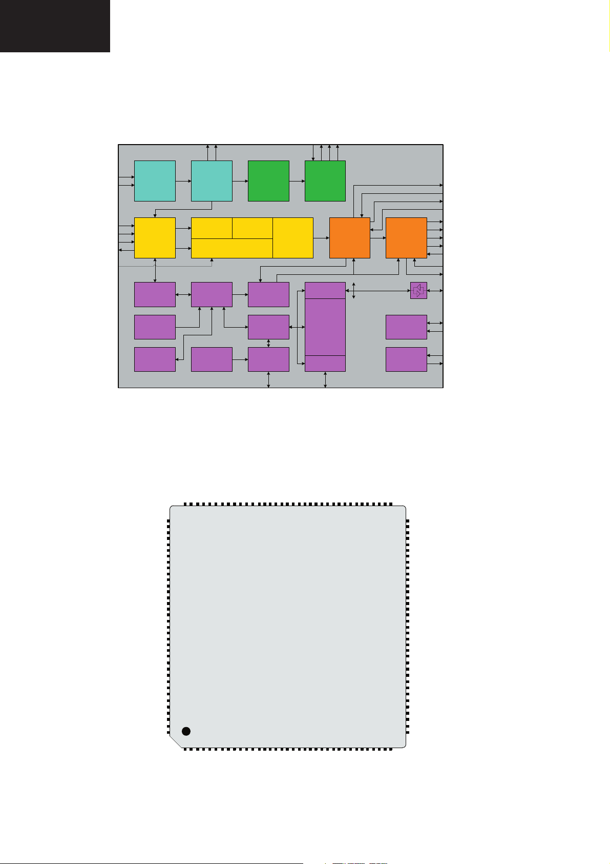
LC-26GA6E/LC-26BV6E
,
LC-26GA5E
LC-32GA6E/LC-32BV6E
LC-32GA5E
LC-37GA6E
1. IC1001 (RH-IXB595WJZZ)
1.1. VCT Block Diagram IC1001
MAJOR ICs INFORMATION
R
E
K
C
G
F
I
A
T
S
T
W
A
U
B
E
N
O
I
U
P
S
A
A
S
IFIN+
IFIN-
CVBS in
YCbCr in
RGB in
CVBS out
IF
Frontend
Video
Frontend
IF
Processor
Comb
Filter
Component
Interface
Demodulator
Color
Decoder
Sound
Panorama
Scaler
Processor
656 in
Slicer
24kB
Char ROM
Bus
Arbiter
Display
Generator
CPU
8051
I2C Master/
Watchdog
20kB XRAM
256kB
Prog ROM
Memory
Interface
ADB, DB, PSENQ,
WRQ, RDQ
PSWEQ
I/O-Ports
1.2. Pinning IC1001
Audio
Slave
Timer
CRT
PWM
ADC
UART
RTC
Pxy
Display &
Deflection
Processor
Video
Backend
Reset & Test
Logic
Clock
Generator
656 out
PROT
HOUT
HFLB
VERT
EW
SVM
RGB out
RGB in
SENSE
RSW
I2C
RESETQ
TEST
XTAL1
XTAL2
IFIN+
IFIN-
VREFIF
TAGC
AIN1R / SIF
AIN1L
AIN2R
AIN2L
AIN3R
AIN3L
AOUT2R
AOUT2L
AOUT1R
AOUT1L
SPEAKERR
SPEAKERL
VREFAU
VSUP8.0AU
GND
GND
VSUP5.0BE
TEST / SUBW
VERT+
VERT-
RSW2
RSW1
SENSE
GNDM
FBIN
SVMOUT
ROUT
GOUT
EW
RIN
GIN
BIN
VSUP5.0FE
RESETQ
VSUP5.0IF
106
107
108
109
110
111
112
113
114
115
116
117
118
119
120
121
122
123
124
125
126
127
128
129
130
131
132
133
134
135
136
137
138
139
140
141
142
143
144
123456789
VRD
XREF
BOUT
P25 / 656HIO
P26 / 656VIO
P30 / 656IO0
P31 / 656IO1
P32 / 656IO2
VSUP3.3EIO
GNDEIO
P33 / 656IO3
P34 / 656IO4
78
77
3132333435
RDQ
WRQ
ADB19
OCF
P35 / 656IO5
747576
73
72
P36 / 656IO6
71
P37 / 656IO7
70
VIN11
69
VIN10
68
VIN9
67
VIN8
66
VIN7
VIN6
65
64
VIN5
VIN4
63
VIN3
62
61
VIN2
60
VIN1
59
VOUT1
VOUT2
58
VOUT3
57
56
VSUP1.8FE
GND
55
GND
54
VSUP3.3FE
53
52
EXTIFQ
51
XROMQ
P10
50
P11
49
P12
48
P13
47
P14
46
P15
45
P16
44
P17
43
P20
42
P21
41
40
SCL
39
SDA
38
DFVBL / FIELD
37
PWMV
36
ALE
RSTQ
VSUP3.3DIG
GND
GND
VSUP1.8DIG
XTAL1
XTAL2
P22
P23
PSENQ
ADB10
DB7
DB6
DB5
DB4
DB3
DB2
DB1
ADB3
ADB2
DB0
ADB0
ADB1
P24 / 656CLKIO
98
96
97
99
101
100
102
103
104
105
909192
939495
80
81
79
82
83848586878889
VCT 49xyI, VCT 48xyI XM
10111213141516
GND
GND
HFLB
SAFETY
GNDDAC
VSUP3.3IO
VSUP3.3BE
VSUP3.3DAC
HOUT
ADB11
VPROT
ADB9
ADB8
1718192021
ADB13
ADB14
ADB17
PSWEQ
242526
27
22
23
ADB18
ADB16
ADB15
STOPQ
30
28
29
ADB7
ADB5
ADB4
ADB6
ENEQ
ADB12
60
Page 61
1.3. Description of Pins IC1001
p
NC = not connected
LV = if not used, leave vacant
OBL = obligatory; connect as described in circuit diagram
IN = Input Pin
OUT = Output Pin
SUPPLY = Supply Pin
LC-26GA6E/LC-26BV6E
LC-26GA5E
LC-32GA6E/LC-32BV6E
LC-32GA5E
LC-37GA6E
Pin No. Pin Name Ty pe Connection
(If not used)
PSSDIP88-1PYPSSDIP88-1PZPMQFP144-2
XM
Short Description
1 88 128 GND SUPPLY OBL Ground Platform
2 87 129 VSUP5.0BE SUPPLY OBL Supply Voltage Analog Video Back-end, 5.0 V
3 86 130 TEST /
SUBW
IN
OUT
GND Test Input, reserved for Test
Subwoofer Output
4 85 131 VERT+ OUT GND Differential Vertical Sawtooth Output
5 84 132 VERT- OUT GND Differential Vertical Sawtooth Output
6 83 133 EW OUT GND Vertical Parabola Output
7 82 134 RSW2 OUT LV Range Switch 2 Output
8 81 135 RSW1 OUT LV Range Switch 1 Output
9 80 136 SENSE IN GND Sense ADC Input
10 79 137 GNDM IN GND Reference Ground for Sense ADC
11 78 138 FBIN IN GND Fast Blank Input, Back-end
12 77 139 RIN IN GND Analog Red Input, Back-end
13 76 140 GIN IN GND Analog Green Input, Back-end
14 75 141 BIN IN GND Analog Blue Input, Back-end
15 74 142 SVMOUT OUT VSUP5.0BE Scan Velocity Modulation Output
16 73 143 ROUT OUT VSUP5.0BE Analog Red Output
17 72 144 GOUT OUT VSUP5.0BE Analog Green Output
18 71 1 BOUT OUT VSUP5.0BE Analog Blue Output
19 70 2 VRD OBL Reference Voltage for RGB DACs
20 69 3 XREF OBL Reference Current for RGB DACs
21 68 4 VSUP3.3BE SUPPLY OBL Supply Voltage Analog Video Back-end, 3.3 V
22 67 5 GND SUPPLY OBL Ground Platform
23 66 6 GND SUPPLY OBL Ground Platform
24 65 7 VSUP3.3IO SUPPLY OBL Supply Voltage I/O Ports, 3.3 V
25 64 8 VSUP3.3DAC SUPPLY OBL Supply Voltage Video DACs, 3.3 V
26 63 9 GNDDAC SUPPLY OBL Ground Video DACs
27 62 10 SAFETY IN GND Safety Input
61
Page 62

LC-26GA6E/LC-26BV6E
LC-26GA5E
LC-32GA6E/LC-32BV6E
LC-32GA5E
LC-37GA6E
1.3. Description of Pins IC1001, continued
Pin No. Pin Name Type Connection
PSSDIP88-1PYPSSDIP88-1PZPMQFP144-2
XM
(If not used)
Short Description
28 61 11 HFLB IN HOUT Horizontal Flyback Input
29 60 12 HOUT OUT LV Horizontal Drive Output
30 59 13 VPROT IN GND Vertical Protection Input
37 PWMV OUT LV PWM Vertical Output
38 DFVBL OUT LV Dynamic Focus Vertical Blanking Output
2
31 58 39 SDA IN/OUT OBL I
32 57 40 SCL IN/OUT OBL I
C Bus Data Input/Output
2
C Bus Clock Input/Output
33 56 41 P21 IN/OUT LV Port 2, Bit 1 Input/Output
34 55 42 P20 IN/OUT LV Port 2, Bit 0 Input/Output
35 54 43 P17 IN/OUT LV Port 1, Bit 7 Input/Output
36 53 44 P16 IN/OUT LV Port 1, Bit 6 Input/Output
37 52 45 P15 IN/OUT LV Port 1, Bit 5 Input/Output
38 51 46 P14 IN/OUT LV Port 1, Bit 4 Input/Output
39 50 47 P13 IN/OUT LV Port 1, Bit 3 Input/Output
40 49 48 P12 IN/OUT LV Port 1, Bit 2 Input/Output
41 48 49 P11 IN/OUT LV Port 1, Bit 1 Input/Output
42 47 50 P10 IN/OUT LV Port 1, Bit 0 Input/Output
43 46 53 VSUP3.3FE SUPPLY OBL Supply Voltage Analog Video Front-end, 3.3 V
44 45 54 GND SUPPLY OBL Ground Platform
45 44 55 GND SUPPLY OBL Ground Platform
46 43 56 VSUP1.8FE SUPPLY OBL Supply Voltage Analog Video Front-end, 1.8 V
47 42 57 VOUT3 OUT LV Analog Video 3 Output
48 41 58 VOUT2 OUT LV Analog Video 2 Output
49 40 59 VOUT1 OUT LV Analog Video 1 Output
50 39 60 VIN1 IN GND Analog Video 1 Input
51 38 61 VIN2 IN GND Analog Video 2 Input
52 37 62 VIN3 IN GND Analog Video 3 Input
53 36 63 VIN4 IN GND Analog Video 4 Input
54 35 64 VIN5 IN GND Analog Video 5 Input
55 34 65 VIN6 IN GND Analog Video 6 Input
56 33 66 VIN7 IN GND Analog Video 7 Input
57 32 67 VIN8 IN GND Analog Video 8 Input
58 31 68 VIN9 IN GND Analog Video 9 Input
62
Page 63

1.3. Description of Pins IC1001, continued
LC-26GA6E/LC-26BV6E
LC-26GA5E
LC-32GA6E/LC-32BV6E
LC-32GA5E
LC-37GA6E
Pin No. Pin Name Type Connection
(If not used)
PSSDIP88-1PYPSSDIP88-1PZPMQFP144-2
XM
Short Description
59 30 69 VIN10 IN GND Analog Video 10 Input
60 29 70 VIN11 IN GND Analog Video 11 Input
61 28 98 P23 IN/OUT LV Port 2, Bit 3 Input/Output
62 27 99 P22 IN/OUT LV Port 2, Bit 2 Input/Output
63 26 100 XTAL2 OUT OBL Analog Crystal Output
64 25 101 XTAL1 IN OBL Analog Crystal Input
65 24 102 VSUP1.8DIG SUPPLY OBL Supply Voltage Digital Core, 1.8 V
66 23 103 GND SUPPLY OBL Ground Platform
67 22 104 GND SUPPLY OBL Ground Platform
68 21 105 VSUP3.3DIG SUPPLY OBL Supply Voltage Digital Core, 3.3 V
69 20 106 VSUP5.0IF SUPPLY OBL Supply Voltage IF ADC, 5.0 V
70 19 107 VSUP5.0FE SUPPLY OBL Supply Voltage Analog IF Front-end, 5.0 V
71 18 108 RESETQ IN/OUT OBL Reset
72 17 109 IFIN+ IN VREF
73 16 110 IFIN- IN VREF
IF
IF
Input/Output
Differential IF Input
Differential IF Input
74 15 111 VREFIF OBL Reference Voltage, IF ADC
75 14 112 TAGC OUT LV Tuner AGC Output
76 13 113 AIN1R /
SIF
IN/OUT GND Analog Audio 1 Input, Right
Analog 2nd Sound IF Output
77 12 114 AIN1L IN GND Analog Audio 1 Input, Left
78 11 115 AIN2R IN GND Analog Audio 2 Input, Right
79 10 116 AIN2L IN GND Analog Audio 2 Input, Left
117 AIN3R IN GND Analog Audio 3 Input, Right
118 AIN3L IN GND Analog Audio 3 Input, Left
119 AOUT2R OUT LV Analog Audio 2 Output, Right
120 AOUT2L OUT LV Analog Audio 2 Output, Left
80 9 AIN3R /
AOUT2R
IN /
OUT
LV Analog Audio 3 Input, Right
Analog Audio 2 Output, Right
81 8 AIN3L /
AOUT2L
IN /
OUT
LV Analog Audio 3 Input, Left
Analog Audio 2 Output, Left
82 7 121 AOUT1R OUT LV Analog Audio 1 Output, Right
83 6 122 AOUT1L OUT LV Analog Audio 1 Output, Left
84 5 123 SPEAKERR OUT LV Analog Loudspeaker Output, Right
85 4 124 SPEAKERL OUT LV Analog Loudspeaker Output, Left
63
Page 64
LC-26GA6E/LC-26BV6E
LC-26GA5E
LC-32GA6E/LC-32BV6E
LC-32GA5E
LC-37GA6E
1.3. Description of Pins IC1001, continued
Pin No. Pin Name Type Connection
(If not used)
PSSDIP88-1PYPSSDIP88-1PZPMQFP144-2
XM
Short Description
86 3 125 VREFAU OBL Reference Voltage, Audio
87 2 126 VSUP8.0AU SUPPLY OBL Supply Voltage Analog Audio, 8.0 V
88 1 127 GND SUPPLY OBL Ground Platform
71 P37 /
656IO7
72 P36 /
656IO6
73 P35 /
656IO5
74 P34 /
656IO4
75 P33 /
656IO3
IN/OUT LV Port 3, Bit 7 Input/Output
Digital 656 Bus 7 Input/Output
IN/OUT LV Port 3, Bit 6 Input/Output
Digital 656 Bus 6 Input/Output
IN/OUT LV Port 3, Bit 5 Input/Output
Digital 656 Bus 5 Input/Output
IN/OUT LV Port 3, Bit 4 Input/Output
Digital 656 Bus 4 Input/Output
IN/OUT LV Port 3, Bit 3 Input/Output
Digital 656 Bus 3 Input/Output
76 GNDEIO SUPPLY OBL Ground Extended I/O Ports
77 VSUP3.3EIO SUPPLY OBL Supply Voltage Extended I/O Ports, 3.3 V
78 P32 /
656IO2
79 P31 /
656IO1
80 P30 /
656IO0
81 P26 /
656VIO
82 P25 /
656HIO
83 P24 /
656CLKIO
IN/OUT LV Port 3, Bit 2 Input/Output
Digital 656 Bus 2 Input/Output
IN/OUT LV Port 3, Bit 1 Input/Output
Digital 656 Bus 1 Input/Output
IN/OUT LV Port 3, Bit 0 Input/Output
Digital 656 Bus 0 Input/Output
IN/OUT LV Port 2, Bit 6 Input/Output
Digital 656 Vsync Input/Output
IN/OUT LV Port 2, Bit 5 Input/Output
Digital 656 Hsync Input/Output
IN/OUT LV Port 2, Bit 4 Input/Output
Digital 656 Clock Input/Output
31 ADB19 OUT LV Address Bus 19 Output
21 ADB18 OUT LV Address Bus 18 Output
19 ADB17 OUT LV Address Bus 17 Output
22 ADB16 OUT LV Address Bus 16 Output
23 ADB15 OUT LV Address Bus 15 Output
18 ADB14 OUT LV Address Bus 14 Output
17 ADB13 OUT LV Address Bus 13 Output
26 ADB12 OUT LV Address Bus 12 Output
14 ADB11 OUT LV Address Bus 11 Output
96 ADB10 OUT LV Address Bus 10 Output
64
Page 65

1.3. Description of Pins IC1001, continued
LC-26GA6E/LC-26BV6E
LC-26GA5E
LC-32GA6E/LC-32BV6E
LC-32GA5E
LC-37GA6E
Pin No. Pin Name Type Connection
(If not used)
PSSDIP88-1PYPSSDIP88-1PZPMQFP144-2
XM
Short Description
15 ADB9 OUT LV Address Bus 9 Output
16 ADB8 OUT LV Address Bus 8 Output
27 ADB7 OUT LV Address Bus 7 Output
28 ADB6 OUT LV Address Bus 6 Output
29 ADB5 OUT LV Address Bus 5 Output
30 ADB4 OUT LV Address Bus 4 Output
84 ADB3 OUT LV Address Bus 3 Output
85 ADB2 OUT LV Address Bus 2 Output
86 ADB1 OUT LV Address Bus 1 Output
87 ADB0 OUT LV Address Bus 0 Output
88 DB0 IN/OUT LV Data Bus 0 Input/Output
89 DB1 IN/OUT LV Data Bus 1 Input/Output
90 DB2 IN/OUT LV Data Bus 2 Input/Output
91 DB3 IN/OUT LV Data Bus 3 Input/Output
92 DB4 IN/OUT LV Data Bus 4 Input/Output
93 DB5 IN/OUT LV Data Bus 5 Input/Output
94 DB6 IN/OUT LV Data Bus 6 Input/Output
95 DB7 IN/OUT LV Data Bus 7 Input/Output
32 RDQ OUT LV Data Read Enable
Output
33 WRQ OUT LV Data Write Enable Output
34 OCF OUT LV Opcode Fetch Output
35 ALE OUT LV Address Latch Enable Output
36 RSTQ OUT LV Internal CPU Reset Output
97 PSENQ OUT LV Program Store Enable Output
20 PSWEQ OUT LV Program Store Write Enable Output
51 XROMQ IN OBL External ROM Enable Input
52 EXTIFQ IN LV Enable External Interface Input
24 STOPQ IN LV Stop CPU Input
25 ENEQ IN LV Enable Emulation Input
65
Page 66

LC-26GA6E/LC-26BV6E
LC-26GA5E
LC-32GA6E/LC-32BV6E
LC-32GA5E
LC-37GA6E
2. IC1301 (VHITA2024++-1)
2.1. Pinning IC1301
+5VGEN
DCAP2
DCAP1
V5D
AGND1
REF
OVERLOADB
AGND2
V5A
OAOUT1
INV1
MUTE
NC
OAOUT2
INV2
BIASCAP
AGND3
SLEEP
36
1
2
3
4
5
6
7
8
9
10
11
12
13
14
15
16
17
18
CPUMP
35
PGND1
34
NC
33
VDDA
32
NC
31
OUTP1
30
VDD1
29
VDD1
28
OUTM1
27
OUTM2
VDD2
26
25
VDD2
OUTP2
24
NC
23
DGND
22
NC
21
PGND2
20
FAULT
19
2.2. Pin Description IC1301
Pin Function Description
2, 3 DCAP2, DCAP1 Charge pump switching pins. DCAP1 (pin 3) is a free running 300kHz square
4, 9 V5D, V5A Digital 5VDC, Analog 5VDC
5, 8,
17
6 REF Internal reference voltage; approximately 1.0 VDC.
7 OVERLOADB A logic low output indicates the input signal has overloaded the amplifier.
10, 14 OAOUT1, OAOUT2 Input stage output pins.
11, 15 INV1, INV2 Single-ended inputs. Inputs are a “virtual” ground of an inverting opamp with
12 MUTE When set to logic high, both amplifiers are muted and in idle mode. When low
16 BIASCAP Input stage bias voltage (approximately 2.4VDC).
18 SLEEP When set to logic high, device goes into low power mode. If not used, this pin
19 FAULT A logic high output indicates thermal overload, or an output is shorted to ground,
20, 35 PGND2, PGND1 Power Grounds (high current)
22 DGND Digital Ground. Connect to AGND locally (near the TA2024).
24, 27;
31, 28
25, 26,
29, 30
13, 21,
23, 32,
34
33 VDDA Analog 12VDC
36 CPUMP Charge pump output (nominally 10V above VDDA)
1 5VGEN Regulated 5VDC source used to supply power to the input section (pins 4 and 9).
AGND1, AGND2,
OUTP2 & OUTM2;
OUTP1 & OUTM1
VDD2, VDD2
VDD1, VDD1
wave between VDDA and DGND (12Vpp nominal). DCAP2 (pin 2) is level shifted
10 volts above DCAP1 (pin 3) with the same amplitude (12Vpp nominal),
frequency, and phase as DCAP1.
Analog Ground
AGND3
approximately 2.4VDC bias.
(grounded), both amplifiers are fully operational. If left floating, the device stays in
the mute mode. This pin should be tied to GND if not used.
should be grounded
or another output.
Bridged output pairs
Supply pins for high current H-bridges, nominally 12VDC.
NC Not connected. Not bonded internally.
66
Page 67
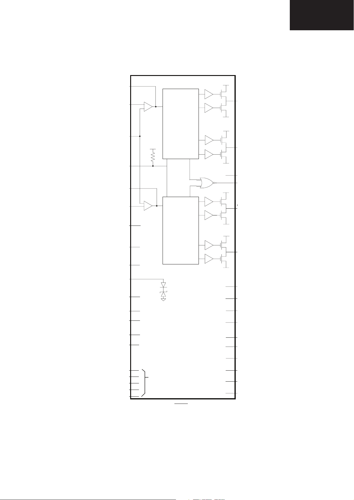
2.3. Block Diagram IC1301
O
O
LC-26GA6E/LC-26BV6E
LC-26GA5E
LC-32GA6E/LC-32BV6E
LC-32GA5E
LC-37GA6E
10
11
16
Processing
&
Modulation
5V
12
VDD1
31
PGND1
VDD1
28
PGND1
19
7
14
15
6
REF
Processing
&
3
DCAP1
Modulation
VDD2
24
PGND2
VDD2
27
2
DCAP2
SLEEP
18
4
17
V5D
5
AGND1
9
V5A
8
AGND2
AGND3
5V
13
21
NC
23
32
34
CPUMP
VDDA
DGND
+5VGEN
VDD1
VDD1
PGND1
VDD2
VDD2
PGND2
PGND2
36
33
22
1
30
29
35
25
26
20
67
Page 68

LC-26GA6E/LC-26BV6E
LC-26GA5E
LC-32GA6E/LC-32BV6E
LC-32GA5E
LC-37GA6E
3. IC2201 (VHISII9021+-1Q)
3.1. Pinning IC1904
SiI 9021
144-Pin
TQFP
(Top View)
68
Page 69
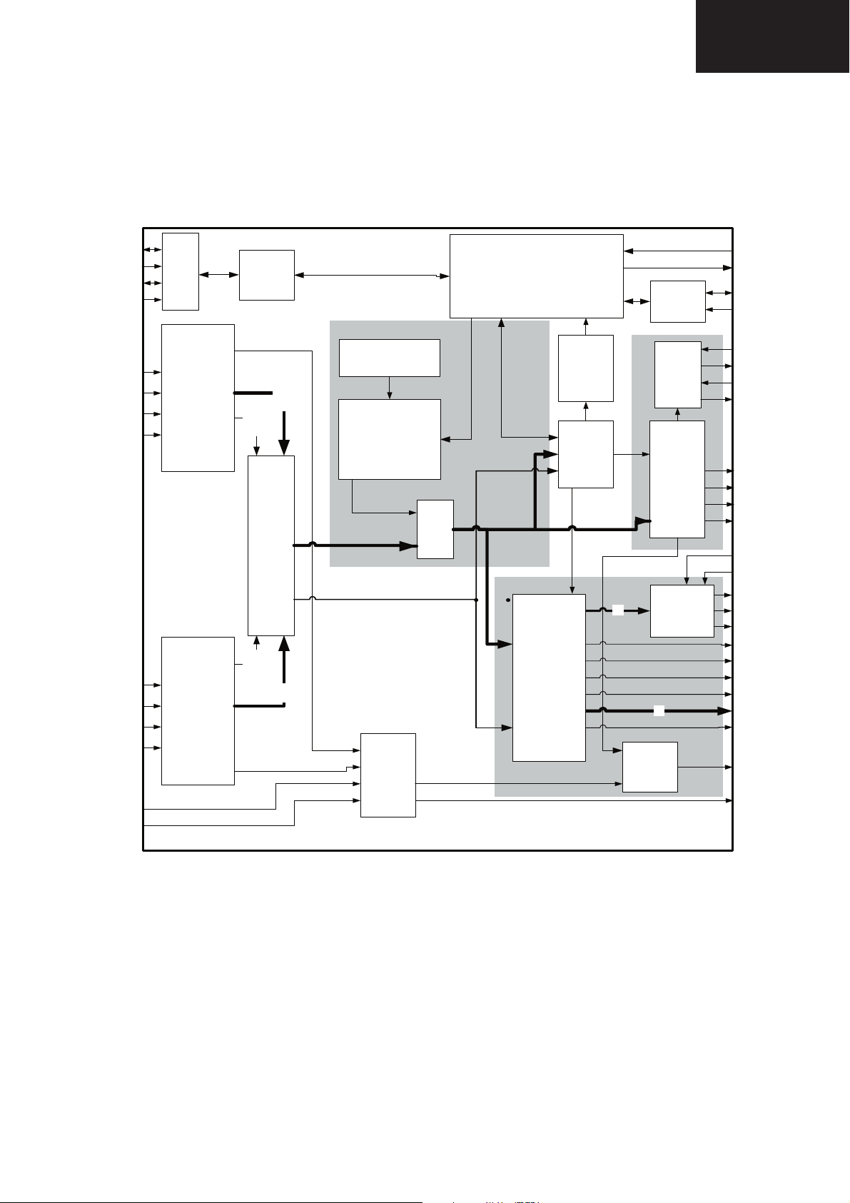
3.2. Block Diagram IC1904
LC-26GA6E/LC-26BV6E
LC-26GA5E
LC-32GA6E/LC-32BV6E
LC-32GA5E
LC-37GA6E
PanelLink
TMDS
SiliconImage Confidential
PanelLink
TMDS
For
Sharp
Internal use Only
69
Page 70
LC-26GA6E/LC-26BV6E
LC-26GA5E
LC-32GA6E/LC-32BV6E
LC-32GA5E
LC-37GA6E
4. IC2201 (RH-IXB372WJZZ)
4.1. Pinning IC2201
D3
D2
D1
D0
A19
A18
A17
A16
VDDPA2
VSSPA2
VDDPA1
VSSPA1
XO
VDDQ3
VSSQ
VDD1
VSS
A15
A14
A13
A12
A11
A10
A9
A8
A7
VDD1
VSS
VDDQ3
VSSQ
A6
A5
A4
A3
A2
A1
NMI
WR
RD
ROM OE
ROM WE
CS0
CS1
PORTA7
PORTA6
PORTA5
PORTA4
PORTA3
PORTA2
PORTA1
PORTA0
D4D5D6D7D8D9D10
154
155
156
157
158
159
160
161
162
163
164
165
166
167
168
169
XI
170
171
172
173
174
175
176
177
178
179
180
181
182
183
184
185
186
187
188
189
190
191
192
193
194
195
196
197
198
199
200
201
202
203
204
205
206
207
208
123456789101112131415161718192021222324252627282930313233343536373839404142434445464748495051
153
152
151
150
D11
149
D12
148
VSS
147
VDD1
146
D13
D14
D15NCNCNCNCNCTESTE N
142
143
144
145
141
140
139
138
137
VSS
136
VDD1
135
VSSQ
134
VDDQ3
133
RES ET_N
132
DOR0
131
DOR1
130
PW1306
(Top View)
DOR2
129
DOR3
128
DOR4
127
DOR5
126
DOR6
125
DOR7
124
VSSQ
123
VDDQ3
122
DOG0
121
DOG1
120
DOG2
119
DOG3
118
DOG4
117
DOG5
116
DOG6
115
DOG7
114
DOB0
113
DOB1
112
DOB2
111
DOB3
110
DOB4
109
DOB5
108
DCLKNEG
107
DCLK
106
VSSQ
105
104
103
102
101
100
52
99
98
97
96
95
94
93
92
91
90
89
88
87
86
85
84
83
82
81
80
79
78
77
76
75
74
73
72
71
70
69
68
67
66
65
64
63
62
61
60
59
58
57
56
55
54
53
VDDQ3
DEN
DHS
DVS
DOB6
DOB7
DER0
DER1
VSS
VDD1
DER2
DER3
DER4
DER5
DER6
DER7
DEG0
DEG1
DEG2
DEG3
VSSQ
VDDQ3
DEG4
DEG5
DEG6
DEG7
DEB0
DEB1
VSS
VDD1
DEB2
DEB3
VCLK
DEB4
DEB5
VSSQ
VDDQ3
DEB6
DEB7
HSYNC
VSYNC
PORTD0
PORTD1
PORTD2
PORTD3
PORTD4
PORTD5
PORTD6
PORTD7
VPEN
TX D
RXD
NC
NC
NC
NC
NC
NC
NC
NC
AVDD
AGND
DVDD1
DGND1
DVDD1
DGND1
AGND
NC
AGND
AVDD
PVD
PVD
PVD
FILT
PGND
PGND
DGND1
DVDD1
PGND
ALVDD
ALVDD
AVDD
ALGND
ALGND
AVDD
RAIN
AGND
AGND
AVDD
AGND
AVDD
GAIN
AGND
AVDD
AGND
AGND
SOGIN
AVDD
BAIN
AGND
AVDD
AGND
AGND
AVDD
Figure 2-1 Pin Locations
CONFIDENTIAL
70
Page 71

4.2. Video Image Processor Block Diagram, IC2201
LC-26GA6E/LC-26BV6E
LC-26GA5E
LC-32GA6E/LC-32BV6E
LC-32GA5E
LC-37GA6E
DRRGB (2 3:0)
DGRGB(2 3:0)
DVS, DHS,
DEN, DCLK
CS
D
A
RxDTx D
NMI
(1:0 )
(15 :0)
(19 :1)
Por tA & PortD (7:0 )
UART
Interrupt
Processor ROM/
16-Bit
2-Wire
IR
GPIO PWM
Control ler
Ti me r s
Watchdog a nd
RAM Interface
Microprocessor Bus
Microprocessor
Serial
Decode r
OSD
Memory Out Bus
Memory
Inte rface
Process or
Bu ff e r
Memory
Memory In Bus
Color
Space
Ex p an d e r
Timing
Dis p la y
Ge ne rat or
PW1306
Color
Tables
Lookup
Internal Block Diagram
and
OSD
Gain
XI XO
Os cillator
RESET
Re s e t
MCLK DCLK UCLK
Res et
PLL and
Pow erOn
Color
Matrix
Video
Scalin g &
En h a nc e m e n t
Auto
Image
CSC
HSHSYNC,
VS
CLK
ADC
A/DCla mp
SOY
SOYIN
PLL
Strippe r
FILT
R/Pr
Sync
Processing
VSYNC
A/DCla mp
G/Y
A/DCla mp
B/Pb
CONFIDENTIAL
71
Page 72

LC-26GA6E/LC-26BV6E
LC-26GA5E
LC-32GA6E/LC-32BV6E
LC-32GA5E
LC-37GA6E
4.3. Description of Pins IC2201
Table 2-1 Signal Descriptions for the Analog Interface Pins
Name Pin Ty pe Function
RAIN 37 AI Red/Green/Blue Analog Inputs. These pins receive the Red, Green and
GAIN 43 AI
BAIN 50 AI
SOGIN 44 AI
FILT 23 AI
HSYNC 65 DIS
VSYNC 64 DIS
Blue, or YPbPr/YCbCr/YUV analog signals from the analog video source.
For proper operation of the clamp feature, these inputs must be
AC-coupled.
Analog Sync-On-Green or Sync-On-Luma input. Allows recovery of the
HSYNC signal when this pin is AC-coupling to the Green (Red or Blue)
analog signal source. If not used, this pin should be left unconnected.
External PLL Loop Filter. When using the on-chip PLL, this pin must be
connected to an external filter network.
Horizontal Synchronization Input. This digital input signal controls the
horizontal scan frequency by synchronizing the start of the horizontal
scan. The logic polarity of this signal is controlled by the HSPOL bit.
Vertical Synchronization Input. This digital signal controls the vertical scan
frequency.
Ta bl e 2 -2
provides detailed Display/Even Port pin descriptions.
Table 2-2 Display/Even Port Pin Descriptions
Name Pin(s) Ty pe Function
DPort Pixel Clock. Output clock for the display port pixel data. DCLK is
enabled by the DCLKEN bit and can be inverted by the DCPOL bit. DCLK
DCLK 106 OSR
DCLKNEG 107 OSR
DVS 101 OS
DHS 102 OS
DEN 103 OS
can be set to run at ½ pixel rate, for dual pixel output mode, by setting the
DCK2EN bit. The internal DCLK clock domain can be disabled by the
DCLKOFF bit to reduce power consumption.
DPort Pixel Clock.
DPort Vertical Sync. DVS can be either active-high or active-low depending
on the VSPOL bit. Width and timing is controlled by the VPLSE and VDLY
registers.
DPort Vertical Sync. DHS can be either active-high or active-low depending
on the HSPOL bit. Sync width can be controlled by the HPLSE register.
DPort Pixel Enable. This signal is active whenever valid data is present.
The polarity is specified by the DENPOL bit.
72
CONFIDENTIAL
Page 73

4.3. Description of Pins IC2201, continued
Table 2-2 Display/Even Port Pin Descriptions (continued)
Name Pin(s) Ty pe Function
DER0 98 OSR
DER1 97 OSR
DER2 94 OSR
LC-26GA6E/LC-26BV6E
LC-26GA5E
LC-32GA6E/LC-32BV6E
LC-32GA5E
LC-37GA6E
DER3 93 OSR
DER4 92 OSR
DER5 91 OSR
DER6 90 OSR
DER7 89 OSR
DEG0 88 OSR
DEG1 87 OSR
DEG2 86 OSR
DEG3 85 OSR
DEG4 82 OSR
DEG5 81 OSR
DEG6 80 OSR
DEG7 79 OSR
DEPort Red Pixel Data. In dual pixel output mode these pins are the EVEN
red outputs.
DEPort Green Pixel Data. In dual pixel output mode these pins are the
EVEN green outputs.
DEB0 78 OSR
DEB1 77 OSR
DEB2 74 OSR
DEB3 73 OSR
DEB4 71 OSR
DEB5 70 OSR
DEB6 67 OSR
DEB7 66 OSR
DEPort Blue Pixel Data. In dual pixel output mode these pins are the EVEN
blue outputs.
CONFIDENTIAL
73
Page 74

LC-26GA6E/LC-26BV6E
LC-26GA5E
LC-32GA6E/LC-32BV6E
LC-32GA5E
LC-37GA6E
4.3. Description of Pins IC2201, continued
Table 2-3 Port D Pin Descriptions
Name Pin(s) Type Function
VCLK 72 I/O D5
VPEN 55 I/O D5
PORTD0 63 I/O D5
PORTD1 62 I/O D5
PORTD2 61 I/O D5
PORTD3 60 I/O D5
PORTD4 59 I/O D5
PORTD5 58 I/O D5
PORTD6 57 I/O D5
PORTD7 56 I/O D5
DVPort Pixel Clock. The VCLK pin is used for DV port image capture.
The polarity can be selected by the VCLKPOL bit.
DVPort Pixel Enable. Used when external flow control capture mode is
enabled by the EXTFCE bit. When VPEN is active, the input data is valid.
The polarity can be selected by the PENPOL bit. Use of this pin allows
non-contiguous input data.
PORTD(7:0) can be used as GPO (Output Only).
Ta bl e 2 -4
provides detailed Display/Odd Port pin descriptions.
Table 2-4 Display/Odd Port Pin Descriptions
Name Pin(s) Type Function
DOR0 131 I/O SR5
DOR1 130 I/O SR5
DOR2 129 I/O SR5
DOR3 128 I/O SR5
DOR4 127 I/O SR5
DOR5 126 I/O SR5
DOR6 125 I/O SR5
DOR7 124 I/O SR5
DOPort Red Pixel Data. In dual pixel output mode these pins are the ODD
red outputs. In single pixel output mode these pins are not used.
74
CONFIDENTIAL
Page 75

4.3. Description of Pins IC2201, continued
Table 2-4 Display/Odd Port Pin Descriptions (continued)
Name Pin(s) Ty pe Function
DOG0 121 I/O SR5
DOG1 120 I/O SR5
DOG2 119 I/O SR5
LC-26GA6E/LC-26BV6E
LC-26GA5E
LC-32GA6E/LC-32BV6E
LC-32GA5E
LC-37GA6E
DOG3 118 I/O SR5
DOG4 117 I/O SR5
DOG5 116 I/O SR5
DOG6 115 I/O SR5
DOG7 114 I/O SR5
DOB0 113 I/O SR5
DOB1 112 I/O SR5
DOB2 111 I/O SR5
DOB3 110 I/O SR5
DOB4 109 I/O SR5
DOB5 108 I/O SR5
DOB6 100 I/O SR5
DOB7 99 I/O SR5
DOPort Green Pixel Data. In dual pixel output mode these pins are the
ODD green outputs. In single pixel output mode these pins are not used.
DOPort Blue Pixel Data. In dual pixel output mode these pins are the ODD
blue outputs. In single pixel output mode these pins are not used.
Ta bl e 2 -5 provides detailed Microprocessor Interface pin descriptions.
Table 2-5 Microprocessor Interface Pin Descriptions
Name
WR 195 I/O D5
RD 196 I/O D5
ROMOE 197 OS
ROMWE 198 OS
CS0 199 I/O D5
CS1 200 I/O D5
NMI 194 ID 5
Pin(s) Type Function
Write Enable. Low indicates a write to external RAM or other devices.
Read Enable. Low indicates a read to external RAM or other devices.
ROM Output Enable. Low output indicates a read from external ROM.
ROM Write Enable. Low indicates a write to external ROM.
Miscellaneous Chip Select 0. Low selects external devices.
Miscellaneous Chip Select 1. When EXTRAMEN=0, low selects external
devices.
Chip select for external RAM. When EXTRAMEN=1, low selects external
RAM. (RAMCS)
Non-Maskable Interrupt. A high input triggers a non-maskable interrupt to
the on-chip microprocessor.
75
CONFIDENTIAL
Page 76
LC-26GA6E/LC-26BV6E
LC-26GA5E
LC-32GA6E/LC-32BV6E
LC-32GA5E
LC-37GA6E
4.3. Description of Pins IC2201, continued
Table 2-5 Microprocessor Interface Pin Descriptions (continued)
Name
A1 193 I/O D5
A2 192 I/O D5
A3 191 I/O D5
A4 190 I/O D5
A5 189 I/O D5
A6 188 I/O D5
A7 183 I/O D5
A8 182 I/O D5
A9 181 I/O D5
A10 180 I/O D5
A11 179 I/O D5
A12 178 I/O D5
A13 177 I/O D5
A14 176 I/O D5
A15 175 I/O D5
A16 164 I/O D5
A17 163 I/O D5
A18 162 I/O D5
A19 161 I/O D5
D0 160 I/O D5
D1 159 I/O D5
D2 158 I/O D5
D3 157 I/O D5
D4 156 I/O D5
D5 155 I/O D5
D6 154 I/O D5
D7 153 I/O D5
D8 152 I/O D5
D9 151 I/O D5
D10 150 I/O D5
D11 149 I/O D5
D12 148 I/O D5
D13 145 I/O D5
D14 144 I/O D5
D15 143 I/O D5
Pin(s) Type Function
Microprocessor address bus output bits (19:1).
Microprocessor 16-bit bidirectional data bus.
76
CONFIDENTIAL
Page 77

4.3. Description of Pins IC2201, continued
Ta bl e 2 -6 provides detailed Peripheral Interface pin descriptions.
Table 2-6 Peripheral Interface Pin Descriptions
Name Pin(s) Ty pe Function
General-purpose I/O port bit controlled by PADAT0 and PAEN0. This pin
PORTA0 208 I/O U5
PORTA1 207 I/O U5
PORTA2 206 I/O U5
PORTA3 205 I/O U5
PORTA4 204 I/O U5
PORTA5 203 I/O U5
PORTA6 202 I/O U5
PORTA7 201 I/O D5
RXD 53 I/O U5
TXD 54 I/O U5
has one other possible function when EXTRAMEN=1.
When EXTRAMEN=1 and PAEN0=0, PORTA1 is microprocessor address
bit 0 (A0).
General-purpose I/O port bit controlled by PADAT1 and PAEN1. This pin
has one other possible function when EXTRAMEN=1.
When EXTRAMEN=1 and PAEN1=0, PORTA1 is microprocessor byte-high
enable (BHEN)
General-purpose I/O port bit controlled by PADAT2 and PAEN2.
General-purpose I/O port bit controlled by PADAT3 and PAEN3. This pin
can also function as an external clock source for DCLK (DCLKEXT) when
both the internal PLLs are disabled or when DPLLBYP=1.
General-purpose I/O port bit controlled by PADAT4 and PAEN4. This pin
has one other possible function when IREN=1.
When IREN=1 and PAEN4=1, this pin can function as an input to the onchip IR receiver 0. (IRRCVR0)
General-purpose I/O port bit controlled by PADAT5 and PAEN5. This pin
has other possible functions depending on the IREN, EIEN registers. When
EIEN=1 and PAEN5=1, this pin can function as an external interrupt to the
on-chip CPU. When IREN=1 and PAEN5=1, this pin can function as an
input to the on-chip IR receiver 1 (IRRCVR1). When DPLLBYP=1 and
PAEN=0, this pin becomes the output of the DCLK PLL. This output can be
routed through an external spread spectrum chip and then back into port
A3 (DCLK input) to implement spread spectrum.
General-purpose I/O port bit controlled by PADAT6 and PAEN6. This pin
has one other possible function when PREF1EN=1.
When PREF1EN=1 and PAEN6=0, PORTA6 is a variable duty-cycle pulse
reference generator (PWM) output controlled by PREF1HI and PREF1LO.
General-purpose I/O port bit controlled by PADAT7 and PAEN7. This pin
has one other possible function when PREF0EN=1.
When PREF0EN=1 and PAEN7=0, PORTA7 is a variable duty-cycle pulse
reference generator (PWM) output controlled by PREF0HI and PREF0LO.
Serial Receive Data. RXD is the serial receive data for the on-chip serial
port. This pin can also function as the 2-wire master data pin when
2WMEN=16.
Serial Transmit Data. TXD is the serial transmit data for the on-chip serial
port. This pin can also function as the 2-wire master clock output pin when
2WMEN=16.
LC-26GA6E/LC-26BV6E
LC-26GA5E
LC-32GA6E/LC-32BV6E
LC-32GA5E
LC-37GA6E
Ta bl e 2 -7
provides detailed Miscellaneous pin descriptions.
Table 2-7 Miscellaneous Pin Descriptions
Name Pin(s) Ty pe Function
TESTEN 137 ID 5
RESET_N 132 BOD
XI 169 I
XO 170 O
Test Mode Enable. Connect to ground for normal operation.
Reset Output. RESET_N is a bidirectional pin that can be used to either
drive external logic in the system or receive an external reset signal.
Crystal Input. Connect to external crystal. XI can also function as the MCLK
input LVTTL-level signal from an external oscillator.
Crystal Output. Connect to external crystal.
77
CONFIDENTIAL
Page 78

LC-26GA6E/LC-26BV6E
LC-26GA5E
LC-32GA6E/LC-32BV6E
LC-32GA5E
LC-37GA6E
4.3. Description of Pins IC2201, continued
Ta bl e 2 -8 provides detailed Power and Ground pin descriptions.
Table 2-8 Power and Ground Pin Descriptions
Name
VDD1
VSS
VDDQ3
VSSQ
VDDPA1 167 P
VDDPA2 165 P
VSSPA1 168 P
VSSPA2 166 P
PVD 22, 24, 26 P
PGND 21, 25, 27 P
DVDD1 1, 3, 20 P
DGND1 2, 4, 19 P
ALVDD 28, 29 P
ALGND 30, 31 P
AVD D
AGND
Pin(s) Typ e Function
75, 95, 135, 146,
173, 184
76, 96, 136, 147,
174, 185
68, 83, 104, 122,
133, 171, 186
69, 84, 105, 123,
134, 172, 187
6, 18, 32, 33, 36,
39, 41, 46, 48,
52
9, 12, 34, 35, 38,
40, 42, 45, 47,
49, 51
P
P
P
P
P
P
1.8V digital core power.
Digital core ground.
3.3V digital I/O power.
Digital I/O ground.
1.8V analog clock generator power.
1.8V analog clock generator power.
Clock generator analog ground.
Clock generator analog ground.
1.8V PLL power.
PLL ground.
1.8V ADC digital power.
ADC digital ground.
1.8V ADC PLL power.
ADC PLL ground.
3.3V ADC analog power.
ADC analog ground.
78
CONFIDENTIAL
Page 79

5. IC6004 (RH-IXB064WJZZ)
5.1. FRC Pin Confi guration IC6004
LC-26GA6E/LC-26BV6E
LC-26GA5E
LC-32GA6E/LC-32BV6E
LC-32GA5E
LC-37GA6E
VSSP7
VDDP7
TMS
TDO/SVMOFF
TCLK
INTR
656I02
656I12
656I22
656I32
656I42
656I52
656I62
656I72
CLKIN2
UVIN0
UVIN1
UVIN2
UVIN3
VSSP8
VDDP8
VDD8M
VSSD60
VSSD61
VDDD60
VDDD61
UVIN4
UVIN5
UVIN6
UVIN7
656i0/YIN0
VSSP9
VDDP9
AUOUT
VSSA1
VDDA2
AYOUT
VSSA2
VDDA3
AVOUT
VSSA3
VSSA4
VDDA4
VSSD5
VDDD5
NC
NC
SCL
SDA
NC
NC
108107106105 104103102101100 99 98 97 96 95 94 93
109
110
111
NC
112
113
TDI
114
115
116
117
118
119
120
121
122
123
124
125
126
127
128
129
130
131
132
133
134
135
136
137
138
139
140
141
NC
142
143
144
1 2 3 4 5 6 7 8 9 10 11 12 13 14 15 16 17 18 19 20 21 22 23 24 25 26 27 28 29 30 31 32 3 3 34 35 36
NC
TEST
656i1/YIN1
656i2/YIN2
VIN
656i3/YIN3
656i4/YIN4
VDDP0
VSSP0
HIN
656i5/YIN5
656i6/YIN6
656i7/YIN7
CLKIN
VDDD0
VSSD0
FAMOUS
FRC 9419A
FRC 9428A
FRC 9429A
AVI
VDDAPLL
VDDA1
VSSA0
ASVMOUT
VDDA0
VSSD4
VDDD4
UVOUT0
UVOUT1
UVOUT2
UV
OUT3
92 91 90 89 88 87 86 85 8 4 83 82 81 80 79 78 77 76 75 74 73
RGBOUT8
RGBOUT9
VDDP1
VSSP1
XOUT
XIN
VDDD11
VDDD10
VSSD1
VSSAPLL
VSSP6
VDDP6
RGBOUT6
RGBOUT7
UVOUT4/INTR
NC
UVOUT5
AVO/ITR
RGBOUT4
RGBOUT5
NC
VOUT
NC
72
71
70
69
68
67
66
65
64
63
62
61
60
59
58
57
56
55
54
53
52
51
50
49
48
47
46
45
44
43
42
41
40
39
38
37
HOUT
UVOUT6
VDDP5
VSSP52
VSSP51
VSSP50
UVOUT7
UVOUT8
VDDD31
VDDD30
VSSD31
VSSD30
UVOUT9
CLKF20
YOUT0
YOUT1
YOUT2
YOUT3
VDDP4
YOUT4
VSSP4
YOUT5
YOUT6
NC
VSSP3
VDDP3
VSSD2
VDDD2
YOUT7
YOUT8
YOUT9
RGBOUT0
RGBOUT1
RGBOUT2
RGBOUT3
RESET
VDDP2
VSSP2
CLKOUT
79
Page 80

LC-26GA6E/LC-26BV6E
LC-26GA5E
LC-32GA6E/LC-32BV6E
LC-32GA5E
LC-37GA6E
5.2. Block Diagram IC6004
UVIN0
UVIN1
UVIN2
UVIN3
UVIN4
UVIN5
UVIN6
UVIN7
CLKIN
HIN
VIN
AVI
656I0/
YIN0
656I1/
YIN1
656I2/
YIN2
656I3/
YIN3
656I4/
YIN4
656I5/
YIN5
656I6/
YIN6
656I7/
YIN7
656I02
656I12
656I22
656I32
656I42
656I52
656I62
656I72
CLKIN2
126
127
128
129
137
138
139
140
14
10
5
17
142
3
4
6
7
11
12
13
117
118
119
120
121
122
123
124
125
ISS
ITU656/ITU601
Test-controller,
Memory bist
TCLK TMSTDO
CLKF20
61
Decoder
Input Processing
HDTV
Bypass
8:4:4
8:8:8
MUX
DCE
Contrast
LSE
CTE
TDI SCL SDA
XOUT XIN
24 23
Xtal
Oscillator
LL-PLLISM
H-/V-
Prescaler
Global
Motion-,
Still-,
Stock-
Detection
8:8:8
Frame
Generator
Pattern
Generator
Curtain
Generator
Brightness
I2C
Interface
105 106114111115113
648 MHz
clock
648 MHz
DTO
Clock Sync Generation
Noise
Reduction
Local Motion
Detection
Filmmode
Detection
Pixelmixer
Chip Control
C800
Controller
to pin 33/78
116
INTR
Divider
Divider
Free-running Clocks
Line-locked Clocks
data buffer
eDRAM
Memory
Controller
FRC 9419A
FRC 9428A
FRC 9429A
FAMOUS
Display Processing
Matrix
Saturation
Tint
Control
39
RESET
VOUT
CLKOUT
HOUT
36 34 35 33
Output Processing
Output
Sync
Controller
data buffer
Motion
Tracking
Vector
Memory
Line
Block
Converter
H-postscaler
H-panorama
Generator
NCE
SVM
Controller
Interpolation
Converter
V-postscaler
4:2:2
V-panorama
Generator
Bit
Reduction
Delay Adjust
Output
Data
Frame
Rate
Block
Line
2D LSE
MEX
ITU656
ITU601
Encoder
GAIN GAIN GAIN GAIN
SVM DAC Y DAC U DAC V DAC
88
ASVMOUT
AYOU T
AVOU TAUOU T
AVO/INTR
979194
27
RGBOUT9
28
RGBOUT8
29
RGBOUT7
30
RGBOUT6
31
RGBOUT5
32
RGBOUT4
40
RGBOUT3
41
RGBOUT2
42
RGBOUT1
43
RGBOUT0
44
YOUT9
45
YOUT8
46
YOUT7
52
YOUT6
53
YOUT5
55
YOUT4
57
YOU T3
58
YOU T2
59
YOUT1
60
YOUT0
UVOUT9
62
UVOUT8
67
UVOUT7
68
73
UVOUT6
76
UVOUT5
78
UVOUT4/INTR
81
UVOUT3
82
UVOUT2
83
UVOUT1
84
UVOUT0
80
Page 81
5.3. Description of Pins IC6004
NC = not connected, leave vacant
LV = not used, leave vacant
LC-26GA6E/LC-26BV6E
LC-26GA5E
LC-32GA6E/LC-32BV6E
LC-32GA5E
LC-37GA6E
Pin No. Pin Name Type Connection
PMQFP144-4
1NCNC
2 LV Test, do not use
3 656I1/YIN1 I LV (pull
4 656I2/YIN2 I LV (pull
5 VIN I LV (pull
6 656I3/YIN3 I LV (pull
7 656I4/YIN4 I LV (pull
8 VDDP0 S Supply digital pad (3.3 V)
9 VSSP0 S Supply digital pad (0 V)
10 HIN I LV (pull
(If not used)
down)
down)
down)
down)
down)
down)
Short Description
Digital (luminance) input
Digital (luminance) input
Vertical sync input
Digital (luminance) input
Digital (luminance) input
Horizontal sync input
11 656I5/YIN5 I LV (pull
down)
12 656I6/YIN6 I LV (pull
down)
13 656I7/YIN7 I LV (pull
down)
14 CLKIN I Clock input (max. 81.0 MHz)
15 VDDD0 S Supply digital pad (1.8 V)
16 VSSD0 S Supply digital pad (0 V)
17 AVI I LV (pull
down)
18 VDDAPLL S Supply analog PLL (1.8 V)
19 VSSAPLL S Supply analog PLL (0 V)
20 VSSD1 S Supply digital core (0 V)
21 VDDD10 S Supply digital core (1.8 V)
22 VDDD11 S Supply digital core (1.8 V)
Digital (luminance) input
Digital (luminance) input
Digital (luminance) input [MSB]
Active video input
23 XIN I Crystal connection 1
81
Page 82
LC-26GA6E/LC-26BV6E
LC-26GA5E
LC-32GA6E/LC-32BV6E
LC-32GA5E
LC-37GA6E
5.3. Description of Pins IC6004, continued
Pin No. Pin Name Type Connection
PMQFP144-4
24 XOUT O LV (pull
25 VSSP1 S Supply digital pad (0 V)
26 VDDP1 S Suplly digital pad (3.3 V)
27 RGBOUT9 O LV Tristate (SELOMODE=0)
28 RGBOUT8 O LV Tristate (SELOMODE=0)
29 RGBOUT7 O LV Tristate (SELOMODE=0)
30 RGBOUT6 O LV Tristate (SELOMODE=0)
(If not used)
down)
Short Description
Crystal connection 2
Digital (red: SELRB=0; blue: SELRB=1;)
Output [MSB](SELOMODE=1)
Digital (red: SELRB=0; blue: SELRB=1;)
Output (SELOMODE=1)
Digital (red: SELRB=0; blue: SELRB=1;)
Output (SELOMODE=1)
Digital (red: SELRB=0; blue: SELRB=1;)
Output (SELOMODE=1)
31 RGBOUT5 O LV Tristate (SELOMODE=0)
Digital (red: SELRB=0; blue: SELRB=1;)
output (SELOMODE=1)
32 RGBOUT4 O LV Tristate (SELOMODE=0)
Digital (red: SELRB=0; blue: SELRB=1;)
Output (SELOMODE=1)
33 AVO/ITR O LV Active video output (CPUIRQ=0)
Interrupt signal output from μC (CPUIRQ=1)
Static 0 (CPUIRQ=2)
Static 1 (CPUIRQ=3)
34 VOUT O LV Vertical sync output
35 HOUT O LV Horizontal sync output.
(Synchronized to 40.5-81 MHz CLKOUTSEL72=1)
(Synchronized to 20.25-40.5 MHz
CLKOUTSEL72=0 and CLKOUTSEL=1)
(Synchronized to 15.1875-30.75 MHz
CLKOUTSEL72=0 and CLKOUTSEL=0)
36 CLKOUT O LV Output clock disabled (CLKOUTON=0)
Output clock (max. 81 MHz) (CLKOUT=1)
(40.5-81 MHz CLK
20.25-40.5 MHz CLKOUT72=0 and CLKOUTSEL=1
1515.1875-30.37 MHz CLKOUT72=0 and
CLKOUTSEL=0)
OUT72=1
37 VSSP2 S Supply digital pad (0 V)
38 VDDP2 S Supply digital pad (3.3 V)
82
Page 83

5.3. Description of Pins IC6004, continued
LC-26GA6E/LC-26BV6E
LC-26GA5E
LC-32GA6E/LC-32BV6E
LC-32GA5E
LC-37GA6E
Pin No. Pin Name Type Connection
PMQFP144-4
39 RESET I Reset input
40 RGBOUT3 O LV Tristate (SELOMODE=0)
41 RGBOUT2 O LV Tristate (SELOMODE=0)
42 RGBOUT1 O LV Tristate (SELOMODE=0)
43 RGBOUT0 O LV Tristate (SELOMODE=0)
44 YOUT9 O LV Tristate (ENITUE=0)
(If not used)
Short Description
Digital (red: SELRB=0; blue: SELRB=1;)
Output (SELOMODE=1)
Digital (red: SELRB=0; blue: SELRB=1;)
Output (SELOMODE=1)
Digital (red: SELRB=0; blue: SELRB=1;)
Output (SELOMODE=1)
Digital (red: SELRB=0; blue: SELRB=1;)
Output [LSB] (SELOMODE=1)
Digital (luminance/green) output [MSB] (ENITUE=1)
45 YOUT8 O LV Tristate (ENITUE=0)
Digital (luminance/green) output (ENITUE=1)
46 YOUT7 O LV Tristate (ENITUE=0)
Digital (luminance/green) output (ENITUE=1)
47 VDDD2 S Supply digital core (1.8 V)
48 VSSD2 S Supply digital core (0 V)
49 VDDP3 S Supply digital pad (3.3 V)
50 VSSP3 S Supply digital pad (0 V)
51 NC NC
52 YOUT6 O LV Tristate (ENITUE=0)
Digital (luminance/green) output (ENITUE=1)
53 YOUT5 O LV Tristate (ENITUE=0)
Digital (luminance/green) output (ENITUE=1)
54 VSSP4 S Supply digital pad (0 V)
55 YOUT4 O LV Tristate (ENITUE=0)
Digital (luminance/green) output (ENITUE=1)
56 VDDP4 S Supply digital pad (3.3 V)
57 YOUT3 O LV Tristate (ENITUE=0)
Digital (luminance/green) output (ENITUE=1)
58 YOUT2 O LV Tristate (ENITUE=0)
Digital (luminance/green) output (ENITUE=1)
59 YOUT1 O LV Tristate (ENITUE=0)
Digital (luminance/green) output (ENITUE=1)
83
Page 84

LC-26GA6E/LC-26BV6E
LC-26GA5E
LC-32GA6E/LC-32BV6E
LC-32GA5E
LC-37GA6E
5.3. Description of Pins IC6004, continued
Pin No. Pin Name Type Connection
PMQFP144-4
60 YOUT0 O LV Tristate (ENITUE=0)
61 CLKF20 O LV Output clock 20.25 MHz disabled (CLKF20ON=0)
62 UVOUT9 O LV Tristate (ENITUE=0)
63 VSSD30 S Supply digital core (0 V)
64 VSSD31 S Supply digital core (0 V)
65 VDDD30 S Supply digital core (1.8 V)
66 VDDD31 S Supply digital core (1.8 V)
67 UVOUT8 O LV Tristate (ENITUE=0)
(If not used)
Short Description
Digital (luminance/green) output [LSB] (ENITUE=1)
Output clock 20.25 MHz enabled (CLKF20ON=1)
Digital (chrominance/blue) output [MSB] (ENITUE=1
and SELRB=0)
Digital (chrominance/red) output [MSB] (ENITUE=1
and SELRB=1)
Digital (chrominance/blue) output (ENITUE=1 and
SELRB=0)
Digital (chrominance/red) output (ENITUE=1 and
SELRB=1)
68 UVOUT7 O LV Tristate (ENITUE=0)
Digital (chrominance/blue) output (ENITUE=1 and
SELRB=0)
Digital (chrominance/red) output (ENITUE=1 and
SELRB=1)
69 VSSP50 S Supply digital pad (0 V)
70 VSSP51 S Supply digital pad (0 V)
71 VSSP52 S Supply digital pad (0 V)
72 VDDP5 S Supply digital pad (3.3 V)
73 UVOUT6 O LV Tristate (ENITUE=0)
Digital (chrominance/blue) output (ENITUE=1 and
SELRB=0)
Digital (chrominance/red) output (ENITUE=1 and
SELRB=1)
74 NC NC
75 NC NC
76 UVOUT5 O LV Tristate (ENITUE=0)
Digital (chrominance/blue) output (ENITUE=1 and
SELRB=0)
Digital (chrominance/red) output (ENITUE=1 and
SELRB=1)
77 NC NC
84
Page 85

5.3. Description of Pins IC6004, continued
LC-26GA6E/LC-26BV6E
LC-26GA5E
LC-32GA6E/LC-32BV6E
LC-32GA5E
LC-37GA6E
Pin No. Pin Name Type Connection
PMQFP144-4
78 UVOUT4/
INTR
79 VDDP6 S Supply digital pad (3.3 V)
80 VSSP6 S Supply digital pad (0 V)
81 UVOUT3 O LV Tristate (ENITUE=0)
82 UVOUT2 O LV Tristate (ENITUE=0)
OLV Tristate (ENITUE=0)
(If not used)
Short Description
Digital (chrominance/blue) output (ENITUE=1 and
SELRB=0)
Digital (chrominance/red) output (ENITUE=1 and
SELRB=1)
Interrupt signal output from C (CPUIRQ=5)
Static 0 (CPUIRQ=6)
Static 1 (CPUIRQ=7)
Digital (chrominance/blue) output (ENITUE=1 and
SELRB=0)
Digital (chrominance/red) output (ENITUE=1 and
SELRB=1)
Digital (chrominance/blue) output (ENITUE=1 and
SELRB=0)
Digital (chrominance/red) output (ENITUE=1 and
SELRB=1)
83 UVOUT1 O LV Tristate (ENITUE=0)
Digital (chrominance/blue) output (ENITUE=1 and
SELRB=0)
Digital (chrominance/red) output (ENITUE=1 and
SELRB=1)
84 UVOUT0 O LV Tristate (ENITUE=0)
Digital (chrominance/blue) output [MSB](ENITUE=1
and SELRB=0)
Digital (chrominance/red) output [LSB] (ENITUE=1
and SELRB=1)
85 VDDD4 S Supply digital core (1.8 V)
86 VSSD4 S Supply digital core (0 V)
87 VDDA0 S Supply analog DAC SVM (3.3 V)
88 ASVMOUT O LV Middle level (STANDBY=1)
Analog SVM output (ACTFBL=0 and STANDBY=1)
Analog SVM output (control by SVMOFF possible)
(ACTFBL=1 and STANDBY=0)
89 VSSA0 S Supply analog DAC SVM (0 V)
90 VDDA1 S Supply analog DAC B/U (3.3 V)
91 AUOUT O LV Middle level (STANDBY=0)
Chrominance output (STANBY=1)
92 VSSA1 S Supply analog DAC B/U (0 V)
93 VDDA2 S Supply analog DAC G/Y (3.3 V)
85
Page 86
LC-26GA6E/LC-26BV6E
LC-26GA5E
LC-32GA6E/LC-32BV6E
LC-32GA5E
LC-37GA6E
5.3. Description of Pins IC6004, continued
Pin No. Pin Name Ty pe Connection
PMQFP144-4
94 AYOUT O LV Middle level (STANDBY=0)
95 VSSA2 S Supply analog DAC G/Y (0 V)
96 VDDA3 S Supply analog DAC R/V (3.3 V)
97 AVOUT O LV Middle level (STANDBY=0)
98 VSSA3 S Supply analog DAC R/V (0 V)
99 VSSA4 S Supply analog band gap (0 V)
100 VDDA4 S Supply analogband gap (3.3 V)
101 VSSD5 S Supply digital core (0 V)
102 VDDD5 S Supply digital core (1.8 V)
103 NC NC
104 NC NC
105 SCL I/O I²C bus clk
(If not used)
Short Description
Luminance output (STANDBY=1)
Chrominance output (STANDBY=1)
106 SDA I/O I²C bus data
107 NC NC
108 NC NC
109 VSSP7 S Supply digital pad (0 V)
110 VDDP7 S Supply digital pad (3.3 V)
111 TMS I Connect to
VDD (3.3 V)
112 NC NC
113 TDO/
SVMOFF
114 TDI I Connect to
115 TCLK I Connect to
116 INTR O LV Interrupt signal
O/I LV Test data out (ACTSVMOFF=1)
VSS (0 V)
VDD (3.3 V)
Test mode select (3.3 V)
SVM input signal (ACTSVMOFF=0)
Test data in (0 V)
Test clock (3.3 V)
Static 0 (CPUIRQ2=00)
Static 1 (CPUIRQ2=01)
Interrupt signal output from C (CPUIRQ2= 1x)
117 656I02 I LV (pull
down)
Digital (luminance) input [LSB]
86
Page 87

5.3. Description of Pins IC6004, continued
LC-26GA6E/LC-26BV6E
LC-26GA5E
LC-32GA6E/LC-32BV6E
LC-32GA5E
LC-37GA6E
Pin No. Pin Name Type Connection
PMQFP144-4
118 656I12 I LV (pull
119 656I22 I LV (pull
120 656I32 I LV (pull
121 656I42 I LV (pull
122 656I52 I LV (pull
123 656I62 I LV (pull
124 656I72 I LV (pull
125 CLKIN2 I LV (pull
(If not used)
down)
down)
down)
down)
down)
down)
down)
down)
Short Description
Digital (luminance) input
Digital (luminance) input
Digital (luminance) input
Digital (luminance) input
Digital (luminance) input
Digital (luminance) input
Digital (luminance) input
Clock input [max. 81.0 MHz]
126 UVIN0 I LV (pull
down)
127 UVIN1 I LV (pull
down)
128 UVIN2 I LV (pull
down)
129 UVIN3 I LV (pull
down)
130 VSSP8 S Supply digital core (0 V)
131 VDDP8 S Supply digital core (3.3 V)
132 VDD8M S Supply memory (1.8 V)
133 VSSD60 S Supply digital core (0 V)
134 VSSD61 S Supply digital core (0 V)
135 VDDD60 S Supply digital core (1.8V)
136 VDDD61 S Supply digital core (1.8 V)
137 UVIN4 I LV (pull
down)
Digital (chrominance) input [LSB]
Digital (chrominance) input
Digital (chrominance) input
Digital (chrominance) input
Digital (chrominance) input
138 UVIN5 I LV (pull
down)
139 UVIN6 I LV (pull
down)
140 UVIN7 I LV (pull
down)
Digital (chrominance) input
Digital (chrominance) input
Digital (chrominance) input [MSB]
87
Page 88

LC-26GA6E/LC-26BV6E
LC-26GA5E
LC-32GA6E/LC-32BV6E
LC-32GA5E
LC-37GA6E
5.3. Description of Pins IC6004, continued
Pin No. Pin Name Ty pe Connection
PMQFP144-4
141 NC NC
142 656I0/YIN0 I LV (pull
143 VSSP9 S Supply digital pad (0 V)
144 VDDP9 S Supply digital pad (3.3 V)
(If not used)
down)
Short Description
Digital (luminance) input [LSB]
88
Page 89

LC-26GA6E/LC-26BV6E
LC-26GA5E
LC-32GA6E/LC-32BV6E
LC-32GA5E
LC-37GA6E
LC-26GA6E PARTS LISTING
REPLACEMENT PARTS
Replacement parts which have special safety characteristics are identifi ed in this manual. Electrical
components having such features are identifi ed by in the Replacement Parts Listing.
The use of a substitute replacement part which does not have the same safety characteristics as
the factory recommended is not permitted.
Replacement parts not shown in this service manual may create shock fi re, or other hazards.
!
REF No. PARTS DESCRIPTION * SN CODE EX CODE
Q2015 VSDTC144EE/-1Y DTC144EE J AA AA
Q2016 VSDTC144EE/-1Y DTC144EE J AA AA
Q4101 VS2SD1664Q+-1Y 2SD1664Q J AC AC
Q4103 VS2SA1530AR-1Y 2SA1530AR J AB AB
Q4104 VS2SC3928AR-1Y 2SC3928AR J AB AB
Q4105 VSTP0610T++-1Y TP0610T J AD AD
Q4106 VS2SC3928AR-1Y 2SC3928AR J AB AB
Q4108 VS2SK1826++-1Y 2SK1826 J AC AC
HOW TO ORDER REPLACEMENT PARTS
To have your order completed promptly and correctly please supply the following information.
1. MODEL NUMBER 2. REF. NO.
3. PART NO. 4. DESCRIPTION
5. CODE 6. QUANTITY
MARK *: SPARE PARTS
DELIVERY SECTION
REF No. PARTS DESCRIPTION * SN CODE EX CODE
LCD UNIT
RLCDTA054WJZZ 26" LCD Panel Unit, LC-26GA6E
J - -
PRINTED WIRING BOARDS (Not Replacement Item)
PWB-A
PWB-B
PWB-C
PWB-D
PWB-E
PWB-F
!
PWB-G
!
PWB-H
!
PWB-I
DUNTKC919FE05 LCD CONTROL LC26" KIT
DUNTKD322WE01 HDMI Unit, LC26GA6E
DUNTKD323WE01 Component Unit LC26GA6E
DUNTKD334WE02 MAIN UNIT LC26GA6E
DUNTKD335WE02 OPERATION (Key) UNIT LC26GA6E
DUNTKD336WE02 RC/LED UNIT LC26GA6E
RDENCA134WJZZ POWER SUPPLY UNIT LC26GA6E
RUNTKA094WJZZ INVERTER UNIT PSD-0397 LC26GA6E
RUNTKA095WJZZ INVERTER GND UNIT PSD-0398 LC26GA6E
J - J - J - -
S- S- S- SBG BY
SAZ BN
SAM AY
PWB-A LCD CONTROL UNIT
INTEGRATED CIRCUITS
IC2001 VHiBD4742G+-1Y BD4742G-TR J AD AD
IC2004 RH-iXA870WJZZQ HD64F3687H J AY AY
IC2006 VHiT7SET32U1EY TC7SET32FU(T5L J AC AC
IC2008 VHiBR24L08F-1Y BR24L08F-WE2 J AE AE
IC2010 VHiM62392FP-1Y M62392FP J AM AM
IC2016 VHiLVX125FT-1Y TC74LVX125FT J AG AG
IC2017 VHiLVX125FT-1Y TC74LVX125FT J AG AG
IC2019 VHiLVX125FT-1Y TC74LVX125FT J AG AG
IC4101 RH-iXA706WJZZQ IR3E12M1 J AN AN
IC4102 VHiNJM4580V-1Y NJM4580V J AE AE
IC4107 VHiLP2951CM-1Y LP2951CMX J AL AL
IC4108 VHiPQ1CZ41H-1Y PQ1CZ41H2ZP J AG AG
IC4109 VHiLT1615ES-1Y LT1615ES5 J AP AP
IC4114 VHiLT1617ES-1Y LT1617ES5 J AP AP
IC4116 VHiLTC1872+-1Y LTC1872ES6 J AR AR
IC4501 RH-iXB003WJZZQ LR38878 J BB BB
IC4601 RH-iXB001WJZZQ LR38879 J BD BD
IC4602 RH-iXB272WJZZY 25LC640-I/SN J AM AM
IC4603 VHiT7WH123U-1Y TC7WH123FU J AD AD
IC4901 RH-iXB002WJZZQ KZ4E064311TFP J BB BB
IC4902 RH-iXA986WJZZQ MS81V2600-12TB J BB BB
IC4903 RH-iXB434WJZZY 25LC320-I/SNG J AL AL
IC7704 VHiPQ033EZ1-1Y PQ033EZ01ZP J AF AF
IC7706 VHiPQ033EZ1-1Y PQ033EZ01ZP J AF AF
IC7708 VHiPQ1L503M-1Y PQ1L503M2SP J AD AD
IC7709 VHiBD4742G+-1Y BD4742G-TR J AD AD
IC7711 VHiPQ1CZ21H-1Y PQ1CZ21H2ZP J AH AH
TRANSISTORS
Q2002 VSDTC144EE/-1Y DTC144EE J AA AA
Q2003 VSDTC144EE/-1Y DTC144EE J AA AA
Q2004 VSDTC144EE/-1Y DTC144EE J AA AA
Q2011 VSDTC144EE/-1Y DTC144EE J AA AA
Q2012 VSDTC144EE/-1Y DTC144EE J AA AA
Q2013 VS2SK536///-1Y 2SK536 J AE AE
Q2014 VS2SK536///-1Y 2SK536 J AE AE
Q4109 VS2SK1826++-1Y 2SK1826 J AC AC
Q4110 VSSi4884DY+-1Y SI4884DY-T1 J AG AG
Q4112 VS2SB1132Q/-1Y 2SB1132Q J AC AC
Q7701 VSDTC114EE/-1Y DTC114EE J AB AB
DIODES
D2004 VHDMA157A//-1Y MA157A J AC AC
D2005 VHD1SS355//-1Y 1SS355 J AB AB
D4101 VHDHSU119//-1Y HSU119 J AB AB
D4102 VHDLi124+++-1Y Li124 J AC AC
D4103 VHDHSU119//-1Y HSU119 J AB AB
D4104 VHDHSU119//-1Y HSU119 J AB AB
D4105 VHDLi114+++-1Y Li114 J AC AC
D4106 RH-EX1274CEZZY Zener Diode J AB AB
D4107 VHDHSU119//-1Y HSU119 J AB AB
D4108 VHDLi114+++-1Y Li114 J AC AC
D4109 VHDLi124+++-1Y Li124 J AC AC
D4110 VHDDA221///-1Y DA221 J AB AB
D4501 VHDDAN222//-1Y DAN222 J AA AA
D7705 VHDHSU119//-1Y HSU119 J AB AB
D7707 VHDHSU119//-1Y HSU119 J AB AB
D7712 VHDSC8024//-1Y SC8024 J AC AC
D7713 VHDSC8024//-1Y SC8024 J AC AC
D7714 VHDLi114+++-1Y Li114 J AC AC
D7715 VHDDAN222//-1Y DAN222 J AA AA
D7718 VHD1SS355//-1Y 1SS355 J AB AB
D7719 VHD1SS355//-1Y 1SS355 J AB AB
D7720 VHD1SS355//-1Y 1SS355 J AB AB
PACKAGED CIRCUITS
X2001 RCRSC0032TAZZY Crystal AG J -- -X4601 RCRUAA048WJZZY J AK AK
COILS AND FILTERS
L4101 RCiLP0343TAZZY Coil J AD AD
L4102 RCiLCA039WJZZY Coil J AF AF
L4103 RCiLP0355TAZZY Coil J AD AD
L4104 RCiLP0343TAZZY Coil J AD AD
L4105 VPD9M4R7J1R4NY Peaking 4.7μH J AB AB
L4106 RCiLPA001WJZZY Coil J AF AF
L4107 VPBWM220K1R2NY Peaking 22μH J AC AC
L4108 VPBWM220K1R2NY Peaking 22μH J AC AC
L4109 RCiLP0343TAZZY Coil J AD AD
L4110 VPD9M4R7J1R4NY Peaking 4.7μH J AB AB
L7701 RCiLP0343TAZZY Coil J AD AD
L7712 RCiLCA095WJZZY Coil (LC-26/32GA6E) J AD AD
L7712 RCiLP0305TAZZY Coil (LC-37GA6E) J AE AE
L7713 RCiLP0343TAZZY Coil J AD AD
FL2001 RFiLZ0169TAZZY Filter J AD AD
FL4103 RFiLNA002WJZZY Filter J AD AD
FL4651 RFiLNA002WJZZY Filter J AD AD
FL4652 RFiLNA002WJZZY Filter J AD AD
FL4653 RFiLNA002WJZZY Filter J AD AD
FL4654 RFiLNA002WJZZY Filter J AD AD
CAPACITORS
C2001 VCKYCY1EF104ZY 0.1 25V Ceramic J AA AA
C2002 VCKYCY1EF104ZY 0.1 25V Ceramic J AA AA
C2003 VCKYCY1EF104ZY 0.1 25V Ceramic J AA AA
C2004 VCKYCY1EF104ZY 0.1 25V Ceramic J AA AA
C2006 VCCCCY1HH220JY 22p 50V Ceramic J AA AA
C2007 VCCCCY1HH220JY 22p 50V Ceramic J AA AA
C2008 VCKYCY1EF104ZY 0.1 25V Ceramic J AA AA
89
Page 90

LC-26GA6E/LC-26BV6E
LC-26GA5E
LC-32GA6E/LC-32BV6E
LC-32GA5E
LC-37GA6E
REF No. PARTS DESCRIPTION * SN CODE EX CODE
C2009 VCKYCY1HB102KY 1000p 50V Ceramic J AA AA
C2010 VCKYCY1HB103KY 0.01 50V Ceramic J AA AA
C2012 VCKYCY1HB102KY 1000p 50V Ceramic J AA AA
C2013 VCKYCY1HB102KY 1000p 50V Ceramic J AA AA
C2014 VCKYCY1EF104ZY 0.1 25V Ceramic J AA AA
C2015 VCKYCY1EF104ZY 0.1 25V Ceramic J AA AA
C2016 VCKYCY1EF104ZY 0.1 25V Ceramic J AA AA
C2017 VCKYCY1EF104ZY 0.1 25V Ceramic J AA AA
C2020 VCKYCY1HB103KY 0.01 50V Ceramic J AA AA
C2021 VCKYCY1EF104ZY 0.1 25V Ceramic J AA AA
C2022 VCEASY1CN107MY 100 16V Electrolytic J AC AC
C2023 VCKYCY1EF104ZY 0.1 25V Ceramic J AA AA
C2024 VCCCCY1HH102JY 1000p 50V Ceramic J AB AB
C2025 VCKYCY1HB103KY 0.01 50V Ceramic J AA AA
C2032 VCKYCY1EF104ZY 0.1 25V Ceramic J AA AA
C2035 VCKYCY1EF104ZY 0.1 25V Ceramic J AA AA
C2036 VCKYCY1EF104ZY 0.1 25V Ceramic J AA AA
C4101 VCKYCY1EF104ZY 0.1 25V Ceramic J AA AA
C4102 RC-KZA097WJZZY 0.1 25V Ceramic J AD AD
C4103 VCKYCY1EF104ZY 0.1 25V Ceramic J AA AA
C4106 RC-KZ0070TAZZY 4.7 16V Ceramic J AD AD
C4108 RC-KZ0070TAZZY 4.7 16V Ceramic J AD AD
C4109 VCCCCY1HH680JY 68p 50V Ceramic J AA AA
C4110 RC-KZA097WJZZY 0.1 25V Ceramic J AD AD
C4112 VCKYCY1EF104ZY 0.1 25V Ceramic J AA AA
C4114 RC-KZA097WJZZY 0.1 25V Ceramic J AD AD
C4115 RC-KZA097WJZZY 0.1 25V Ceramic J AD AD
C4116 RC-KZA047WJZZY 1 50V Ceramic J AC AC
C4117 VCEASY1CN477MY 470 16V Electrolytic J AD AD
C4119 VCAAPF1DJ226MY 22 20V Electrolytic J AF AF
C4120 VCCCCY1HH5R0CY 5p 50V Ceramic J AA AA
C4121 VCKYCY1EF104ZY 0.1 25V Ceramic J AA AA
C4124 VCCCCY1HH680JY 68p 50V Ceramic J AA AA
C4125 VCKYCY1EF104ZY 0.1 25V Ceramic J AA AA
C4127 RC-KZA097WJZZY 0.1 25V Ceramic J AD AD
C4129 RC-KZA097WJZZY 0.1 25V Ceramic J AD AD
C4135 VCKYTV1CB105KY 1 16V Ceramic J AC AC
C4136 VCAAPF1DJ226MY 22 20V Electrolytic J AF AF
C4137 VCKYCY1EF104ZY 0.1 25V Ceramic J AA AA
C4138 VCEASY1EN227MY 220 25V Electrolytic J AD AD
C4139 VCKYTV1CB105KY 1 16V Ceramic J AC AC
C4141 RC-KZA097WJZZY 0.1 25V Ceramic J AD AD
C4142 VCKYCY1HB102KY 1000p 50V Ceramic J AA AA
C4145 RC-KZ0070TAZZY 4.7 16V Ceramic J AD AD
C4146 VCAAPF1CJ396MY 39 16V Electrolytic J AF AF
C4147 VCKYCY1EF104ZY 0.1 25V Ceramic J AA AA
C4153 RC-KZA097WJZZY 0.1 25V Ceramic J AD AD
C4155 VCKYCY1EF104ZY 0.1 25V Ceramic J AA AA
C4156 VCKYCY1EF104ZY 0.1 25V Ceramic J AA AA
C4159 VCEASY1EN476MY 47 25V Electrolytic J AC AC
C4160 VCEASY1HN106MY 10 50V Electrolytic J AC AC
C4161 RC-KZ0070TAZZY 4.7 16V Ceramic J AD AD
C4162 VCCCCY1HH391JY 390p 50V Ceramic J AB AB
C4163 RC-KZA047WJZZY 1 50V Ceramic J AC AC
C4164 VCKYCY1CF224ZY 0.22 16V Ceramic J AB AB
C4165 VCCCCY1HH101JY 100p 50V Ceramic J AA AA
C4166 VCCCCY1HH221JY 220p 50V Ceramic J AA AA
C4168 RC-KZ0053TAZZY 10 10V Ceramic J AD AD
C4169 VCAAPF1DJ396MY 39 20V Electrolytic J AF AF
C4170 VCCCCY1HH101JY 100p 50V Ceramic J AA AA
C4174 RC-KZ0053TAZZY 10 10V Ceramic J AD AD
C4176 VCKYCY1EF104ZY 0.1 25V Ceramic J AA AA
C4177 VCAAPF1DJ226MY 22 20V Electrolytic J AF AF
C4179 VCKYCY1EF104ZY 0.1 25V Ceramic J AA AA
C4180 VCEASY1EN227MY 220 25V Electrolytic J AD AD
C4181 RC-KZ0070TAZZY 4.7 16V Ceramic J AD AD
C4192 VCKYCY1HB152KY 1500p 50V Ceramic J AA AA
C4195 VCKYCY1EF104ZY 0.1 25V Ceramic J AA AA
C4196 VCEASX1VN226MY 22 35V Electrolytic J AC AC
C4197 VCKYCY1EF104ZY 0.1 25V Ceramic J AA AA
REF No. PARTS DESCRIPTION * SN CODE EX CODE
C4501 VCEASY0JN476MY 47 6.3V Electrolytic J AC AC
C4502 VCKYCY1EF104ZY 0.1 25V Ceramic J AA AA
C4503 VCKYCY1HB102KY 1000p 50V Ceramic J AA AA
C4504 VCEASY0JN476MY 47 6.3V Electrolytic J AC AC
C4505 VCKYCY1EF104ZY 0.1 25V Ceramic J AA AA
C4506 VCKYCY1HB102KY 1000p 50V Ceramic J AA AA
C4507 VCEASY0JN476MY 47 6.3V Electrolytic J AC AC
C4508 VCKYCY1EF104ZY 0.1 25V Ceramic J AA AA
C4509 VCKYCY1HB102KY 1000p 50V Ceramic J AA AA
C4510 VCKYCY1EF104ZY 0.1 25V Ceramic J AA AA
C4511 VCKYCY1EF104ZY 0.1 25V Ceramic J AA AA
C4512 VCCCCY1HH331JY 330p 50V Ceramic J AA AA
C4513 VCCCCY1HH331JY 330p 50V Ceramic J AA AA
C4514 VCKYCY1EF104ZY 0.1 25V Ceramic J AA AA
C4515 VCKYCY1EF104ZY 0.1 25V Ceramic J AA AA
C4516 VCKYCY1HB103KY 0.01 50V Ceramic J AA AA
C4517 VCKYCY1EF104ZY 0.1 25V Ceramic J AA AA
C4518 VCKYCY1EF104ZY 0.1 25V Ceramic J AA AA
C4519 VCCCCY1HH331JY 330p 50V Ceramic J AA AA
C4520 VCCCCY1HH331JY 330p 50V Ceramic J AA AA
C4521 VCKYCY1EF104ZY 0.1 25V Ceramic J AA AA
C4522 VCEASY0JN476MY 47 6.3V Electrolytic J AC AC
C4523 VCKYCY1EF104ZY 0.1 25V Ceramic J AA AA
C4524 VCKYCY1HB102KY 1000p 50V Ceramic J AA AA
C4525 VCCCCY1HH331JY 330p 50V Ceramic J AA AA
C4526 VCKYCY1EF104ZY 0.1 25V Ceramic J AA AA
C4527 VCKYCY1EF104ZY 0.1 25V Ceramic J AA AA
C4528 VCKYCY1HB103KY 0.01 50V Ceramic J AA AA
C4529 VCCCCY1HH331JY 330p 50V Ceramic J AA AA
C4530 VCCCCY1HH331JY 330p 50V Ceramic J AA AA
C4531 VCKYCY1EF104ZY 0.1 25V Ceramic J AA AA
C4532 VCKYCY1EF104ZY 0.1 25V Ceramic J AA AA
C4533 VCKYCY1EF104ZY 0.1 25V Ceramic J AA AA
C4601 VCEASY0JN476MY 47 6.3V Electrolytic J AC AC
C4602 VCKYCY1EF104ZY 0.1 25V Ceramic J AA AA
C4603 VCKYCY1HB102KY 1000p 50V Ceramic J AA AA
C4604 VCKYCY1HB103KY 0.01 50V Ceramic J AA AA
C4605 VCKYCY1HB103KY 0.01 50V Ceramic J AA AA
C4606 VCKYCY1HB103KY 0.01 50V Ceramic J AA AA
C4607 VCKYCY1HB103KY 0.01 50V Ceramic J AA AA
C4608 VCKYCY1HB103KY 0.01 50V Ceramic J AA AA
C4609 VCKYCY1HB103KY 0.01 50V Ceramic J AA AA
C4610 VCKYCY1EF104ZY 0.1 25V Ceramic J AA AA
C4611 VCKYCY1HB103KY 0.01 50V Ceramic J AA AA
C4612 VCKYCY1HB103KY 0.01 50V Ceramic J AA AA
C4613 VCKYCY1HB103KY 0.01 50V Ceramic J AA AA
C4614 VCKYCY1HB102KY 1000p 50V Ceramic J AA AA
C4615 VCKYCY1HB103KY 0.01 50V Ceramic J AA AA
C4616 VCKYCY1HB102KY 1000p 50V Ceramic J AA AA
C4617 VCKYCY1HB103KY 0.01 50V Ceramic J AA AA
C4618 VCKYCY1HB103KY 0.01 50V Ceramic J AA AA
C4619 VCKYCY1EF104ZY 0.1 25V Ceramic J AA AA
C4620 VCEASY0JN476MY 47 6.3V Electrolytic J AC AC
C4621 VCKYCY1EF104ZY 0.1 25V Ceramic J AA AA
C4622 VCEASY0JN476MY 47 6.3V Electrolytic J AC AC
C4623 VCKYCY1EF104ZY 0.1 25V Ceramic J AA AA
C4624 VCKYCY1HB102KY 1000p 50V Ceramic J AA AA
C4625 VCKYCY1EF104ZY 0.1 25V Ceramic J AA AA
C4626 VCKYCY1HB103KY 0.01 50V Ceramic J AA AA
C4651 VCAAPF0JJ107MY 100 6.3V Electrolytic J AF AF
C4652 VCKYCY1EF104ZY 0.1 25V Ceramic J AA AA
C4653 VCAAPF1DJ226MY 22 20V Electrolytic J AF AF
C4654 VCKYCY1EF104ZY 0.1 25V Ceramic J AA AA
C4655 VCAAPF0JJ107MY 100 6.3V Electrolytic J AF AF
C4656 VCKYCY1EF104ZY 0.1 25V Ceramic J AA AA
C4657 VCAAPF1DJ226MY 22 20V Electrolytic J AF AF
C4658 VCKYCY1EF104ZY 0.1 25V Ceramic J AA AA
C4901 VCEASY0JN476MY 47 6.3V Electrolytic J AC AC
C4902 VCKYCY1EF104ZY 0.1 25V Ceramic J AA AA
C4903 VCKYCY1HB102KY 1000p 50V Ceramic J AA AA
90
Page 91
LC-26GA6E/LC-26BV6E
LC-26GA5E
LC-32GA6E/LC-32BV6E
LC-32GA5E
LC-37GA6E
REF No. PARTS DESCRIPTION * SN CODE EX CODE
C4904 VCKYCY1EF104ZY 0.1 25V Ceramic J AA AA
C4905 VCKYCY1EF104ZY 0.1 25V Ceramic J AA AA
C4906 VCKYCY1EF104ZY 0.1 25V Ceramic J AA AA
C4907 VCKYCY1EF104ZY 0.1 25V Ceramic J AA AA
C4908 VCKYCY1EF104ZY 0.1 25V Ceramic J AA AA
C4909 VCKYCY1EF104ZY 0.1 25V Ceramic J AA AA
C4910 VCKYCY1HB103KY 0.01 50V Ceramic J AA AA
C4911 VCKYCY1EF104ZY 0.1 25V Ceramic J AA AA
C4912 VCCCCY1HH331JY 330p 50V Ceramic J AA AA
C4913 VCKYCY1EF104ZY 0.1 25V Ceramic J AA AA
C4914 VCKYCY1HB103KY 0.01 50V Ceramic J AA AA
C4915 VCCCCY1HH331JY 330p 50V Ceramic J AA AA
C4916 VCKYCY1HB102KY 1000p 50V Ceramic J AA AA
C4917 VCKYCY1EF104ZY 0.1 25V Ceramic J AA AA
C4918 VCEASY0JN476MY 47 6.3V Electrolytic J AC AC
C4919 VCKYCY1EF104ZY 0.1 25V Ceramic J AA AA
C4920 VCKYCY1EF104ZY 0.1 25V Ceramic J AA AA
C4921 VCKYCY1HB102KY 1000p 50V Ceramic J AA AA
C4922 VCKYCY1EF104ZY 0.1 25V Ceramic J AA AA
C4923 VCKYCY1EF104ZY 0.1 25V Ceramic J AA AA
C4924 VCKYCY1EF104ZY 0.1 25V Ceramic J AA AA
C4925 VCKYCY1EF104ZY 0.1 25V Ceramic J AA AA
C4926 VCKYCY1EF104ZY 0.1 25V Ceramic J AA AA
C4927 VCKYCY1EF104ZY 0.1 25V Ceramic J AA AA
C4928 VCKYCY1EF104ZY 0.1 25V Ceramic J AA AA
C4929 VCKYCY1EF104ZY 0.1 25V Ceramic J AA AA
C4930 VCKYCY1EF104ZY 0.1 25V Ceramic J AA AA
C4931 VCEASY0JN476MY 47 6.3V Electrolytic J AC AC
C4932 VCKYCY1EF104ZY 0.1 25V Ceramic J AA AA
C4933 VCKYCY1EF104ZY 0.1 25V Ceramic J AA AA
C4934 VCKYCY1EF104ZY 0.1 25V Ceramic J AA AA
C4935 VCKYCY1EF104ZY 0.1 25V Ceramic J AA AA
C4936 VCEASY0JN107MY 100 6.3V Electrolytic J AC AC
C4937 VCKYCY1EF104ZY 0.1 25V Ceramic J AA AA
C4938 VCKYCY1HB102KY 1000p 50V Ceramic J AA AA
C4939 VCKYCY1EF104ZY 0.1 25V Ceramic J AA AA
C4940 VCKYCY1EF104ZY 0.1 25V Ceramic J AA AA
C4941 VCKYCY1EF104ZY 0.1 25V Ceramic J AA AA
C4942 VCKYCY1EF104ZY 0.1 25V Ceramic J AA AA
C4943 VCKYCY1EF104ZY 0.1 25V Ceramic J AA AA
C4944 VCKYCY1HB103KY 0.01 50V Ceramic J AA AA
C4945 VCKYCY1EF104ZY 0.1 25V Ceramic J AA AA
C4946 VCKYCY1EF104ZY 0.1 25V Ceramic J AA AA
C4947 VCKYCY1EF104ZY 0.1 25V Ceramic J AA AA
C4948 VCKYCY1EF104ZY 0.1 25V Ceramic J AA AA
C4949 VCKYCY1HB103KY 0.01 50V Ceramic J AA AA
C4950 VCKYCY1EF104ZY 0.1 25V Ceramic J AA AA
C4951 VCKYCY1EF104ZY 0.1 25V Ceramic J AA AA
C4952 VCKYCY1EF104ZY 0.1 25V Ceramic J AA AA
C4953 VCKYCY1EF104ZY 0.1 25V Ceramic J AA AA
C7701 VCEASY1CN107MY 100 16V Electrolytic J AC AC
C7702 VCKYCY1EF104ZY 0.1 25V Ceramic J AA AA
C7703 VCEASX1CN226MY 22 16V Electrolytic J AC AC
C7704 VCKYCY1EF104ZY 0.1 25V Ceramic J AA AA
C7707 VCEASY1CN226MY 22 16V Electrolytic J AC AC
C7709 VCEASY1CN226MY 22 16V Electrolytic J AC AC
C7713 VCKYCY1EF104ZY 0.1 25V Ceramic J AA AA
C7715 VCKYCY1EF104ZY 0.1 25V Ceramic J AA AA
C7723 VCEASY0JN476MY 47 6.3V Electrolytic J AC AC
C7724 VCEASY0JN476MY 47 6.3V Electrolytic J AC AC
C7725 VCKYCY1HB103KY 0.01 50V Ceramic J AA AA
C7728 VCKYCY1EF104ZY 0.1 25V Ceramic J AA AA
C7729 VCKYCY1EF104ZY 0.1 25V Ceramic J AA AA
C7733 VCEASY1EN107MY 100 25V Electrolytic J AC AC
C7734 VCCCCY1HH681JY 680p 50V Ceramic J AB AB
C7735 VCEASY1CN477MY 470 16V Electrolytic J AD AD
C7736 VCKYCY1EF104ZY 0.1 25V Ceramic J AA AA
C7737 VCKYCY1EF104ZY 0.1 25V Ceramic J AA AA
RESISTORS
REF No. PARTS DESCRIPTION * SN CODE EX CODE
R2001 VRS-CY1JF104JY 100k 1/16W Metal Oxide J AA AA
R2002 VRS-CY1JF000JY 0 1/16W Metal Oxide J AA AA
R2003 VRS-CY1JF223JY 22k 1/16W Metal Oxide J AA AA
R2004 VRS-CY1JF000JY 0 1/16W Metal Oxide J AA AA
R2005 VRS-CY1JF101JY 100 1/16W Metal Oxide J AA AA
R2006 VRS-CJ1JF333JY 33k 1/16W Metal Oxide J AA AA
R2007 VRS-CY1JF222FY 2.2k 1/16W Metal Oxide J AA AA
R2008 VRS-CY1JF223JY 22k 1/16W Metal Oxide J AA AA
R2009 VRS-CY1JF101JY 100 1/16W Metal Oxide J AA AA
R2010 VRS-CY1JF223JY 22k 1/16W Metal Oxide J AA AA
R2011 VRS-CY1JF103JY 10k 1/16W Metal Oxide J AA AA
R2013 VRS-CY1JF393JY 39k 1/16W Metal Oxide J AA AA
R2016 VRS-CY1JF103JY 10k 1/16W Metal Oxide J AA AA
R2016 VRS-CY1JF223JY 22k 1/16W Metal Oxide J AA AA
R2017 VRS-CY1JF394JY 390k 1/16W Metal Oxide J AA AA
R2018 VRS-CY1JF106JY 10M 1/16W Metal Oxide J AA AA
R2019 VRS-CY1JF105JY 1M 1/16W Metal Oxide J AA AA
R2020 VRS-CY1JF101JY 100 1/16W Metal Oxide J AA AA
R2021 VRS-CY1JF101JY 100 1/16W Metal Oxide J AA AA
R2022 VRS-CY1JF101JY 100 1/16W Metal Oxide J AA AA
R2023 VRS-CY1JF104JY 100k 1/16W Metal Oxide J AA AA
R2024 VRS-CY1JF000JY 0 1/16W Metal Oxide J AA AA
R2025 VRS-CY1JF103JY 10k 1/16W Metal Oxide J AA AA
R2026 VRS-CY1JF223JY 22k 1/16W Metal Oxide J AA AA
R2027 VRS-CY1JF000JY 0 1/16W Metal Oxide J AA AA
R2028 VRS-CY1JF000JY 0 1/16W Metal Oxide J AA AA
R2030 VRS-CY1JF473JY 47k 1/16W Metal Oxide J AA AA
R2031 VRS-CY1JF101JY 100 1/16W Metal Oxide J AA AA
R2033 VRS-CY1JF000JY 0 1/16W Metal Oxide J AA AA
R2034 VRS-CY1JF000JY 0 1/16W Metal Oxide J AA AA
R2035 VRS-CY1JF472JY 4.7k 1/16W Metal Oxide J AA AA
R2036 VRS-CY1JF223JY 22k 1/16W Metal Oxide J AA AA
R2037 VRS-CY1JF223JY 22k 1/16W Metal Oxide J AA AA
R2038 VRS-CY1JF333JY 33k 1/16W Metal Oxide J AA AA
R2040 VRS-CY1JF103JY 10k 1/16W Metal Oxide J AA AA
R2041 VRS-CY1JF101JY 100 1/16W Metal Oxide J AA AA
R2042 VRS-CY1JF101JY 100 1/16W Metal Oxide J AA AA
R2044 VRS-CY1JF472JY 4.7k 1/16W Metal Oxide J AA AA
R2045 VRS-CY1JF472JY 4.7k 1/16W Metal Oxide J AA AA
R2046 VRS-CY1JF103JY 10k 1/16W Metal Oxide J AA AA
R2048 VRS-CY1JF101JY 100 1/16W Metal Oxide J AA AA
R2049 VRS-CY1JF101JY 100 1/16W Metal Oxide J AA AA
R2050 VRS-CY1JF683JY 68k 1/16W Metal Oxide J AA AA
R2052 VRS-CY1JF101JY 100 1/16W Metal Oxide J AA AA
R2053 VRS-CY1JF223JY 22k 1/16W Metal Oxide J AA AA
R2054 VRS-CY1JF101JY 100 1/16W Metal Oxide J AA AA
R2056 VRS-CJ1JF101JY 100 1/16W Metal Oxide J AA AA
R2058 VRS-CY1JF000JY 0 1/16W Metal Oxide J AA AA
R2059 VRS-CY1JF000JY 0 1/16W Metal Oxide J AA AA
R2060 VRS-CY1JF000JY 0 1/16W Metal Oxide J AA AA
R2061 VRS-CY1JF101JY 100 1/16W Metal Oxide J AA AA
R2063 VRS-CY1JF101JY 100 1/16W Metal Oxide J AA AA
R2064 VRS-CY1JF101JY 100 1/16W Metal Oxide J AA AA
R2065 VRS-CJ1JF101JY 100 1/16W Metal Oxide J AA AA
R2066 VRS-CY1JF000JY 0 1/16W Metal Oxide J AA AA
R2067 VRS-CY1JF101JY 100 1/16W Metal Oxide J AA AA
R2068 VRS-CY1JF104JY 100k 1/16W Metal Oxide J AA AA
R2069 VRS-CY1JF000JY 0 1/16W Metal Oxide J AA AA
R2070 VRS-CY1JF000JY 0 1/16W Metal Oxide J AA AA
R2071 VRS-CY1JF000JY 0 1/16W Metal Oxide J AA AA
R2072 VRS-CY1JF223JY 22k 1/16W Metal Oxide J AA AA
R2073 VRS-CY1JF000JY 0 1/16W Metal Oxide J AA AA
R2074 VRS-CY1JF473JY 47k 1/16W Metal Oxide J AA AA
R2075 VRS-CY1JF222JY 2.2k 1/16W Metal Oxide J AA AA
R2076 VRS-CY1JF000JY 0 1/16W Metal Oxide J AA AA
R2077 VRS-CY1JF101JY 100 1/16W Metal Oxide J AA AA
R2078 VRS-CY1JF101JY 100 1/16W Metal Oxide J AA AA
R2079 VRS-CY1JF101JY 100 1/16W Metal Oxide J AA AA
R2081 VRS-CY1JF223JY 22k 1/16W Metal Oxide J AA AA
R2088 VRS-CY1JF101JY 100 1/16W Metal Oxide J AA AA
91
Page 92
LC-26GA6E/LC-26BV6E
LC-26GA5E
LC-32GA6E/LC-32BV6E
LC-32GA5E
LC-37GA6E
REF No. PARTS DESCRIPTION * SN CODE EX CODE
R2089 VRS-CY1JF101JY 100 1/16W Metal Oxide J AA AA
R2092 VRS-CY1JF223JY 22k 1/16W Metal Oxide J AA AA
R2093 VRS-CY1JF332JY 3.3k 1/16W Metal Oxide J AA AA
R2607 VRS-CY1JF220JY 22 1/16W Metal Oxide J AA AA
R2608 VRS-CY1JF220JY 22 1/16W Metal Oxide J AA AA
R2609 VRS-CY1JF104JY 100k 1/16W Metal Oxide J AA AA
R2610 VRS-CY1JF104JY 100k 1/16W Metal Oxide J AA AA
R2611 VRS-CY1JF101JY 100 1/16W Metal Oxide J AA AA
R2612 VRS-CY1JF822FY 8.2k 1/16W Metal Oxide J AA AA
R2616 VRS-CY1JF103JY 10k 1/16W Metal Oxide J AA AA
R2618 VRS-CY1JF220JY 22 1/16W Metal Oxide J AA AA
R2620 VRS-CY1JF104JY 100k 1/16W Metal Oxide J AA AA
R2625 VRS-CY1JF101JY 100 1/16W Metal Oxide J AA AA
R2629 VRS-CY1JF000JY 0 1/16W Metal Oxide J AA AA
R2630 VRS-CY1JF472JY 4.7k 1/16W Metal Oxide J AA AA
R2631 VRS-CY1JF472JY 4.7k 1/16W Metal Oxide J AA AA
R2633 VRS-CY1JF101JY 100 1/16W Metal Oxide J AA AA
R2634 VRS-CY1JF101JY 100 1/16W Metal Oxide J AA AA
R2636 VRS-CY1JF102JY 1k 1/16W Metal Oxide J AA AA
R2639 VRS-CY1JF100JY 10 1/16W Metal Oxide J AA AA
R2640 VRS-CY1JF472JY 4.7k 1/16W Metal Oxide J AA AA
R2641 VRS-CY1JF472JY 4.7k 1/16W Metal Oxide J AA AA
R2646 VRS-CY1JF000JY 0 1/16W Metal Oxide J AA AA
R2647 VRS-CY1JF000JY 0 1/16W Metal Oxide J AA AA
R4101 VRS-CY1JF102FY 1k 1/16W Metal Oxide J AA AA
R4102 VRS-CY1JF123FY 12k 1/16W Metal Oxide J AA AA
R4103 VRS-CY1JF472FY 4.7k 1/16W Metal Oxide J AA AA
R4109 VRS-CY1JF562FY 5.6k 1/16W Metal Oxide J AA AA
R4112 VRS-CY1JF153FY 15k 1/16W Metal Oxide J AA AA
R4113 VRS-CY1JF330JY 33 1/16W Metal Oxide J AA AA
R4114 VRS-CY1JF563FY 56k 1/16W Metal Oxide J AA AA
R4115 VRS-CY1JF000JY 0 1/16W Metal Oxide J AA AA
R4118 VRS-CY1JF153FY 15k 1/16W Metal Oxide J AA AA
R4119 VRS-CY1JF362FY 3.6k 1/16W Metal Oxide J AA AA
R4120 VRS-CY1JF103JY 10k 1/16W Metal Oxide J AA AA
R4121 VRS-CY1JF332FY 3.3k 1/16W Metal Oxide J AA AA
R4122 VRS-CY1JF682FY 6.8k 1/16W Metal Oxide J AA AA
R4123 VRS-CY1JF332FY 3.3k 1/16W Metal Oxide J AA AA
R4124 VRS-CY1JF562FY 5.6k 1/16W Metal Oxide J AA AA
R4125 VRS-CY1JF332FY 3.3k 1/16W Metal Oxide J AA AA
R4126 VRS-CY1JF682FY 6.8k 1/16W Metal Oxide J AA AA
R4130 VRS-CH1JF100JY 10 1/16W Metal Oxide J AA AA
R4132 VRS-CY1JF513FY 51k 1/16W Metal Oxide J AA AA
R4133 VRS-CY1JF183FY 18k 1/16W Metal Oxide J AA AA
R4134 VRS-CY1JF821FY 820 1/16W Metal Oxide J AA AA
R4135 VRS-CY1JF103FY 10k 1/16W Metal Oxide J AA AA
R4136 VRS-CY1JF563FY 56k 1/16W Metal Oxide J AA AA
R4137 VRS-CY1JF223FY 22k 1/16W Metal Oxide J AA AA
R4138 VRS-CY1JF152FY 1.5k 1/16W Metal Oxide J AA AA
R4139 VRS-CH1JF330JY 33 1/16W Metal Oxide J AA AA
R4140 VRS-CY1JF623FY 62k 1/16W Metal Oxide J AA AA
R4141 VRS-CY1JF273FY 27k 1/16W Metal Oxide J AA AA
R4142 VRS-CY1JF152FY 1.5k 1/16W Metal Oxide J AA AA
R4143 VRS-CY1JF563FY 56k 1/16W Metal Oxide J AA AA
R4144 VRS-CY1JF273FY 27k 1/16W Metal Oxide J AA AA
R4145 VRS-CY1JF122FY 1.2k 1/16W Metal Oxide J AA AA
R4146 VRS-CH1JF330JY 33 1/16W Metal Oxide J AA AA
R4147 VRS-CH1JF100JY 10 1/16W Metal Oxide J AA AA
R4148 VRS-CY1JF433FY 43k 1/16W Metal Oxide J AA AA
R4149 VRS-CY1JF243FY 24k 1/16W Metal Oxide J AA AA
R4150 VRS-CY1JF151FY 150 1/16W Metal Oxide J AA AA
R4152 VRS-CY1JF163FY 16k 1/16W Metal Oxide J AA AA
R4153 VRS-CY1JF153FY 15k 1/16W Metal Oxide J AA AA
R4154 VRS-CY1JF112FY 1.1k 1/16W Metal Oxide J AA AA
R4155 VRS-CY1JF330FY 33 1/16W Metal Oxide J AA AA
R4156 VRS-CY1JF100JY 10 1/16W Metal Oxide J AA AA
R4157 VRS-CY1JF273FY 27k 1/16W Metal Oxide J AA AA
R4158 VRS-CY1JF273FY 27k 1/16W Metal Oxide J AA AA
R4159 VRS-CY1JF512FY 5.1k 1/16W Metal Oxide J AA AA
R4160 VRS-CY1JF330FY 33 1/16W Metal Oxide J AA AA
REF No. PARTS DESCRIPTION * SN CODE EX CODE
R4161 VRS-CY1JF100JY 10 1/16W Metal Oxide J AA AA
R4162 VRS-CY1JF243FY 24k 1/16W Metal Oxide J AA AA
R4163 VRS-CY1JF513FY 51k 1/16W Metal Oxide J AA AA
R4164 VRS-CY1JF132FY 1.3k 1/16W Metal Oxide J AA AA
R4165 VRS-CH1JF330JY 33 1/16W Metal Oxide J AA AA
R4166 VRS-CH1JF100JY 10 1/16W Metal Oxide J AA AA
R4167 VRS-CY1JF243FY 24k 1/16W Metal Oxide J AA AA
R4168 VRS-CY1JF563FY 56k 1/16W Metal Oxide J AA AA
R4169 VRS-CY1JF152FY 1.5k 1/16W Metal Oxide J AA AA
R4170 VRS-CY1JF223FY 22k 1/16W Metal Oxide J AA AA
R4171 VRS-CY1JF563FY 56k 1/16W Metal Oxide J AA AA
R4172 VRS-CY1JF152FY 1.5k 1/16W Metal Oxide J AA AA
R4174 VRS-CY1JF223FY 22k 1/16W Metal Oxide J AA AA
R4175 VRS-CY1JF623FY 62k 1/16W Metal Oxide J AA AA
R4176 VRS-CY1JF241FY 240 1/16W Metal Oxide J AA AA
R4177 VRS-CH1JF330JY 33 1/16W Metal Oxide J AA AA
R4178 VRS-CY1JF000JY 0 1/16W Metal Oxide J AA AA
R4179 VRS-CY1JF513FY 51k 1/16W Metal Oxide J AA AA
R4180 VRS-CY1JF332FY 3.3k 1/16W Metal Oxide J AA AA
R4181 VRS-CY1JF682FY 6.8k 1/16W Metal Oxide J AA AA
R4182 VRS-CY1JF103FY 10k 1/16W Metal Oxide J AA AA
R4183 VRS-CY1JF153FY 15k 1/16W Metal Oxide J AA AA
R4184 VRS-CY1JF223FY 22k 1/16W Metal Oxide J AA AA
R4186 VRS-CH1JF100JY 10 1/16W Metal Oxide J AA AA
R4187 VRS-CY1JF100JY 10 1/16W Metal Oxide J AA AA
R4188 VRS-CY1JF102FY 1k 1/16W Metal Oxide J AA AA
R4190 VRS-CY1JF473FY 47k 1/16W Metal Oxide J AA AA
R4191 VRS-CY1JF753FY 75k 1/16W Metal Oxide J AA AA
R4192 VRS-CY1JF563FY 56k 1/16W Metal Oxide J AA AA
R4193 VRS-CY1JF102JY 1k 1/16W Metal Oxide J AA AA
R4194 VRS-CY1JF121JY 120 1/16W Metal Oxide J AA AA
R4196 VRS-CY1JF750FY 75 1/16W Metal Oxide J AA AA
R4198 VRS-CY1JF562FY 5.6k 1/16W Metal Oxide J AA AA
R4199 VRS-CY1JF104JY 100k 1/16W Metal Oxide J AA AA
R4200 VRS-CY1JF622FY 6.2k 1/16W Metal Oxide J AA AA
R4201 VRS-CY1JF101FY 100 1/16W Metal Oxide J AA AA
R4202 VRS-CY1JF821FY 820 1/16W Metal Oxide J AA AA
R4203 VRS-CY1JF391FY 390 1/16W Metal Oxide J AA AA
R4204 VRS-CY1JF682FY 6.8k 1/16W Metal Oxide J AA AA
R4205 VRS-CY1JF112FY 1.1k 1/16W Metal Oxide J AA AA
R4206 VRS-TV1JD102JY 1k 1/16W Metal Oxide J AA AA
R4208 VRS-CH1JF100JY 10 1/16W Metal Oxide J AA AA
R4209 VRS-TW2ED221JY 220 1/4W Metal Oxide J AB AB
R4210 VRS-CY1JF103JY 10k 1/16W Metal Oxide J AA AA
R4211 VRS-CY1JF103JY 10k 1/16W Metal Oxide J AA AA
R4213 VRS-TW2ED221JY 220 1/4W Metal Oxide J AB AB
R4216 VRS-CY1JF105FY 1M 1/16W Metal Oxide J AA AA
R4217 VRS-CY1JF103JY 10k 1/16W Metal Oxide J AA AA
R4218 VRS-CY1JF393FY 39k 1/16W Metal Oxide J AA AA
R4219 VRS-CY1JF103JY 10k 1/16W Metal Oxide J AA AA
R4220 VRS-CY1JF105FY 1M 1/16W Metal Oxide J AA AA
R4221 VRS-TW2ED153JY 15k 1/4W Metal Oxide J AA AA
R4222 VRS-TW2ED562JY 5.6k 1/4W Metal Oxide J AB AB
R4223 RR-NZ0027TAZZY Resistor J AC AC
R4224 VRS-TV1JD222JY 2.2k 1/16W Metal Oxide J AA AA
R4225 VRS-CY1JF000JY 0 1/16W Metal Oxide J AA AA
R4226 VRS-TV1JD222JY 2.2k 1/16W Metal Oxide J AA AA
R4227 VRS-TW2ED821JY 820 1/4W Metal Oxide J AB AB
R4228 VRS-CY1JF103JY 10k 1/16W Metal Oxide J AA AA
R4229 VRS-CY1JF105FY 1M 1/16W Metal Oxide J AA AA
R4230 VRS-CY1JF911FY 910 1/16W Metal Oxide J AA AA
R4231 VRS-CY1JF513FY 51k 1/16W Metal Oxide J AA AA
R4233 VRS-CY1JF393FY 39k 1/16W Metal Oxide J AA AA
R4234 VRS-CY1JF154FY 150k 1/16W Metal Oxide J AA AA
R4235 VRS-CY1JF104JY 100k 1/16W Metal Oxide J AA AA
R4238 VRS-CY1JF105JY 1M 1/16W Metal Oxide J AA AA
R4239 VRS-TW2ED682JY 6.8k 1/4W Metal Oxide J AA AA
R4244 VRS-TW2ED562JY 5.6k 1/4W Metal Oxide J AB AB
R4250 VRS-CY1JF100JY 10 1/16W Metal Oxide J AA AA
R4256 VRS-CY1JF104JY 100k 1/16W Metal Oxide J AA AA
92
Page 93

LC-26GA6E/LC-26BV6E
LC-26GA5E
LC-32GA6E/LC-32BV6E
LC-32GA5E
LC-37GA6E
REF No. PARTS DESCRIPTION * SN CODE EX CODE
R4260 VRS-CY1JF332FY 3.3k 1/16W Metal Oxide J AA AA
R4261 VRS-TW2ED101JY 100 1/4W Metal Oxide J AA AA
R4262 VRS-CY1JF103JY 10k 1/16W Metal Oxide J AA AA
R4263 VRS-CY1JF330JY 33 1/16W Metal Oxide J AA AA
R4264 VRS-TW2ED101JY 100 1/4W Metal Oxide J AA AA
R4270 VRS-CY1JF104JY 100k 1/16W Metal Oxide J AA AA
R4271 VRS-CY1JF911FY 910 1/16W Metal Oxide J AA AA
R4272 VRS-CY1JF243FY 24k 1/16W Metal Oxide J AA AA
R4273 VRS-CY1JF513JY 51k 1/16W Metal Oxide J AA AA
R4275 VRS-CY1JF562FY 5.6k 1/16W Metal Oxide J AA AA
R4279 VRS-CY1JF100JY 10 1/16W Metal Oxide J AA AA
R4280 VRS-CY1JF100JY 10 1/16W Metal Oxide J AA AA
R4281 VRS-CY1JF100JY 10 1/16W Metal Oxide J AA AA
R4282 VRS-CH1JF100JY 10 1/16W Metal Oxide J AA AA
R4286 VRS-CJ1JF100JY 10 1/16W Metal Oxide J AA AA
R4288 VRS-CH1JF100JY 10 1/16W Metal Oxide J AA AA
R4501 VRS-CY1JF100JY 10 1/16W Metal Oxide J AA AA
R4502 VRS-CH1JF100JY 10 1/16W Metal Oxide J AA AA
R4505 VRS-CY1JF000JY 0 1/16W Metal Oxide J AA AA
R4506 VRS-CY1JF000JY 0 1/16W Metal Oxide J AA AA
R4507 VRS-CJ1JF101JY 100 1/16W Metal Oxide J AA AA
R4508 VRS-CY1JF330JY 33 1/16W Metal Oxide J AA AA
R4509 VRS-CY1JF101FY 100 1/16W Metal Oxide J AA AA
R4510 VRS-CY1JF101FY 100 1/16W Metal Oxide J AA AA
R4511 VRS-CY1JF101FY 100 1/16W Metal Oxide J AA AA
R4512 VRS-CY1JF101FY 100 1/16W Metal Oxide J AA AA
R4513 VRS-CY1JF101FY 100 1/16W Metal Oxide J AA AA
R4514 VRS-CY1JF000JY 0 1/16W Metal Oxide J AA AA
R4516 VRS-CY1JF133FY 13k 1/16W Metal Oxide J AA AA
R4518 VRS-CY1JF000JY 0 1/16W Metal Oxide J AA AA
R4519 VRS-CH1JF330JY 33 1/16W Metal Oxide J AA AA
R4520 VRS-CJ1JF330JY 33 1/16W Metal Oxide J AA AA
R4521 VRS-CJ1JF330JY 33 1/16W Metal Oxide J AA AA
R4522 VRS-CY1JF101JY 100 1/16W Metal Oxide J AA AA
R4523 VRS-CH1JF330JY 33 1/16W Metal Oxide J AA AA
R4524 VRS-CJ1JF330JY 33 1/16W Metal Oxide J AA AA
R4525 VRS-CY1JF330JY 33 1/16W Metal Oxide J AA AA
R4526 VRS-CY1JF330JY 33 1/16W Metal Oxide J AA AA
R4527 VRS-CY1JF330JY 33 1/16W Metal Oxide J AA AA
R4528 VRS-CY1JF330JY 33 1/16W Metal Oxide J AA AA
R4529 VRS-CY1JF103JY 10k 1/16W Metal Oxide J AA AA
R4531 VRS-CY1JF000JY 0 1/16W Metal Oxide J AA AA
R4601 VRS-CY1JF101FY 100 1/16W Metal Oxide J AA AA
R4602 VRS-CY1JF101FY 100 1/16W Metal Oxide J AA AA
R4603 VRS-CY1JF101FY 100 1/16W Metal Oxide J AA AA
R4604 VRS-CY1JF101FY 100 1/16W Metal Oxide J AA AA
R4605 VRS-CY1JF101FY 100 1/16W Metal Oxide J AA AA
R4606 VRS-CY1JF101FY 100 1/16W Metal Oxide J AA AA
R4607 VRS-CY1JF101FY 100 1/16W Metal Oxide J AA AA
R4608 VRS-CY1JF101FY 100 1/16W Metal Oxide J AA AA
R4609 VRS-CY1JF101FY 100 1/16W Metal Oxide J AA AA
R4610 VRS-CY1JF101FY 100 1/16W Metal Oxide J AA AA
R4611 VRS-CY1JF103JY 10k 1/16W Metal Oxide J AA AA
R4613 VRS-CY1JF473JY 47k 1/16W Metal Oxide J AA AA
R4614 VRS-CJ1JF100JY 10 1/16W Metal Oxide J AA AA
R4615 VRS-CH1JF100JY 10 1/16W Metal Oxide J AA AA
R4616 VRS-CH1JF680JY 68 1/16W Metal Oxide J AA AA
R4617 VRS-CH1JF100JY 10 1/16W Metal Oxide J AA AA
R4618 VRS-CY1JF473JY 47k 1/16W Metal Oxide J AA AA
R4619 VRS-CH1JF680JY 68 1/16W Metal Oxide J AA AA
R4620 VRS-CY1JF270JY 27 1/16W Metal Oxide J AA AA
R4621 VRS-CY1JF270JY 27 1/16W Metal Oxide J AA AA
R4622 VRS-CH1JF680JY 68 1/16W Metal Oxide J AA AA
R4623 VRS-CH1JF680JY 68 1/16W Metal Oxide J AA AA
R4624 VRS-CH1JF680JY 68 1/16W Metal Oxide J AA AA
R4625 VRS-CH1JF680JY 68 1/16W Metal Oxide J AA AA
R4626 VRS-CH1JF680JY 68 1/16W Metal Oxide J AA AA
R4627 VRS-CH1JF680JY 68 1/16W Metal Oxide J AA AA
R4628 VRS-CY1JF333JY 33k 1/16W Metal Oxide J AA AA
R4629 VRS-CY1JF472JY 4.7k 1/16W Metal Oxide J AA AA
REF No. PARTS DESCRIPTION * SN CODE EX CODE
R4630 VRS-CY1JF472JY 4.7k 1/16W Metal Oxide J AA AA
R4631 VRS-CY1JF472JY 4.7k 1/16W Metal Oxide J AA AA
R4632 VRS-CY1JF103JY 10k 1/16W Metal Oxide J AA AA
R4637 VRS-CY1JF101JY 100 1/16W Metal Oxide J AA AA
R4639 VRS-CY1JF103JY 10k 1/16W Metal Oxide J AA AA
R4640 VRS-CY1JF000JY 0 1/16W Metal Oxide J AA AA
R4642 VRS-CY1JF000JY 0 1/16W Metal Oxide J AA AA
R4648 VRS-CY1JF000JY 0 1/16W Metal Oxide J AA AA
R4651 VRS-CY1JF000JY 0 1/16W Metal Oxide J AA AA
R4652 VRS-CY1JF000JY 0 1/16W Metal Oxide J AA AA
R4653 VRS-CY1JF000JY 0 1/16W Metal Oxide J AA AA
R4654 VRS-CY1JF000JY 0 1/16W Metal Oxide J AA AA
R4655 VRS-CY1JF000JY 0 1/16W Metal Oxide J AA AA
R4656 VRS-CY1JF000JY 0 1/16W Metal Oxide J AA AA
R4901 VRS-CH1JF100JY 10 1/16W Metal Oxide J AA AA
R4902 VRS-CH1JF100JY 10 1/16W Metal Oxide J AA AA
R4903 VRS-CY1JF100JY 10 1/16W Metal Oxide J AA AA
R4904 VRS-CH1JF100JY 10 1/16W Metal Oxide J AA AA
R4905 VRS-CY1JF100JY 10 1/16W Metal Oxide J AA AA
R4906 VRS-CH1JF470JY 47 1/16W Metal Oxide J AA AA
R4907 VRS-CH1JF470JY 47 1/16W Metal Oxide J AA AA
R4908 VRS-CH1JF470JY 47 1/16W Metal Oxide J AA AA
R4909 VRS-CH1JF470JY 47 1/16W Metal Oxide J AA AA
R4910 VRS-CH1JF470JY 47 1/16W Metal Oxide J AA AA
R4911 VRS-CH1JF470JY 47 1/16W Metal Oxide J AA AA
R4912 VRS-CH1JF101JY 100 1/16W Metal Oxide J AA AA
R4913 RBLN-A005WJZZY Ferrite Bead J AA AA
R4914 VRS-CJ1JF470JY 47 1/16W Metal Oxide J AA AA
R4915 VRS-CJ1JF470JY 47 1/16W Metal Oxide J AA AA
R4916 VRS-CH1JF470JY 47 1/16W Metal Oxide J AA AA
R4917 VRS-CH1JF470JY 47 1/16W Metal Oxide J AA AA
R4918 VRS-CH1JF470JY 47 1/16W Metal Oxide J AA AA
R4919 VRS-CH1JF470JY 47 1/16W Metal Oxide J AA AA
R4920 VRS-CH1JF470JY 47 1/16W Metal Oxide J AA AA
R4922 VRS-CY1JF103JY 10k 1/16W Metal Oxide J AA AA
R4923 VRS-CY1JF000JY 0 1/16W Metal Oxide J AA AA
R4924 VRS-CY1JF472JY 4.7k 1/16W Metal Oxide J AA AA
R7711 VRS-CY1JF103JY 10k 1/16W Metal Oxide J AA AA
R7714 VRS-CY1JF103JY 10k 1/16W Metal Oxide J AA AA
R7721 VRS-CY1JF101JY 100 1/16W Metal Oxide J AA AA
R7723 VRS-TV1JD000JY 0 1/16W Metal Oxide J AA AA
R7725 VRS-CY1JF103JY 10k 1/16W Metal Oxide J AA AA
R7729 VRS-TV1JD000JY 0 1/16W Metal Oxide J AA AA
R7730 VRS-TV1JD000JY 0 1/16W Metal Oxide J AA AA
R7731 VRS-TV1JD000JY 0 1/16W Metal Oxide J AA AA
R7732 VRS-TV1JD000JY 0 1/16W Metal Oxide J AA AA
R7733 VRS-CY1JF362FY 3.6k 1/16W Metal Oxide J AA AA
R7734 VRS-CY1JF222FY 2.2k 1/16W Metal Oxide J AA AA
R7735 VRS-CY1JF223JY 22k 1/16W Metal Oxide J AA AA
R7744 VRS-CY1JF332FY 3.3k 1/16W Metal Oxide J AA AA
R7745 VRS-CY1JF102FY 1k 1/16W Metal Oxide J AA AA
R7746 VRS-CY1JF332FY 3.3k 1/16W Metal Oxide J AA AA
R7747 VRS-TW2ED330JY 33 1/4W Metal Oxide J AA AA
R7748 VRS-CY1JF103JY 10k 1/16W Metal Oxide J AA AA
R7749 VRS-CY1JF103JY 10k 1/16W Metal Oxide J AA AA
R7750 VRS-TV1JD000JY 0 1/16W Metal Oxide J AA AA
R7751 VRS-CY1JF101JY 100 1/16W Metal Oxide J AA AA
R7752 VRS-CY1JF101JY 100 1/16W Metal Oxide J AA AA
R7755 VRS-TV1JD000JY 0 1/16W Metal Oxide J AA AA
R7756 VRS-TV1JD000JY 0 1/16W Metal Oxide J AA AA
R7759 VRS-TV1JD000JY 0 1/16W Metal Oxide J AA AA
R7760 VRS-TW2ED221JY 220 1/4W Metal Oxide J AB AB
R7761 VRS-TW2ED221JY 220 1/4W Metal Oxide J AB AB
R7762 VRS-TW2ED221JY 220 1/4W Metal Oxide J AB AB
R7763 VRS-TW2ED221JY 220 1/4W Metal Oxide J AB AB
R7770 VRS-CY1JF103JY 10k 1/16W Metal Oxide J AA AA
R7771 VRS-CY1JF473JY 47k 1/16W Metal Oxide J AA AA
MISCELLANEOUS PARTS
FB2001 RBLN-0006TAZZY Ferrite Bead J AB AB
93
Page 94

LC-26GA6E/LC-26BV6E
LC-26GA5E
LC-32GA6E/LC-32BV6E
LC-32GA5E
LC-37GA6E
REF No. PARTS DESCRIPTION * SN CODE EX CODE
FB4101 RBLN-0252TAZZY Ferrite Bead J AA AA
FB4102 RBLN-0252TAZZY Ferrite Bead J AA AA
FB4501 RBLN-0210TAZZY Ferrite Bead J AB AB
FB4502 RBLN-0210TAZZY Ferrite Bead J AB AB
FB4503 RBLN-0210TAZZY Ferrite Bead J AB AB
FB4504 RBLN-0210TAZZY Ferrite Bead J AB AB
FB4505 RBLN-0210TAZZY Ferrite Bead J AB AB
FB4601 RBLN-0210TAZZY Ferrite Bead J AB AB
FB4602 RBLN-A005WJZZY Ferrite Bead J AA AA
FB4603 RBLN-0210TAZZY Ferrite Bead J AB AB
FB4604 RBLN-0210TAZZY Ferrite Bead J AB AB
FB4605 RBLN-0210TAZZY Ferrite Bead J AB AB
FB4901 RBLN-0210TAZZY Ferrite Bead J AB AB
FB4902 RBLN-0210TAZZY Ferrite Bead J AB AB
FB4903 RBLN-0210TAZZY Ferrite Bead J AB AB
FB4904 RBLN-0210TAZZY Ferrite Bead J AB AB
FB7709 RBLN-A005WJZZY Ferrite Bead J AA AA
FB7710 RBLN-0210TAZZY Ferrite Bead J AB AB
FB7712 RBLN-A005WJZZY Ferrite Bead J AA AA
FB7713 RBLN-A005WJZZY Ferrite Bead J AA AA
FB7716 RBLN-A005WJZZY Ferrite Bead J AA AA
FB7717 RBLN-A005WJZZY Ferrite Bead J AA AA
FB7718 RBLN-A005WJZZY Ferrite Bead J AA AA
FB7719 RBLN-A005WJZZY Ferrite Bead J AA AA
FB7720 RBLN-0252TAZZY Ferrite Bead J AA AA
P2001 QPLGN0544FJZZY Plug, 7Pin (AD) J AD AD
P2005 QPLGNA144WJZZY Plug, 20Pin J AF AF
P2006 QPLGNA178WJZZY Plug, 9Pin (SH) J AE AE
P7704 QPLGNA177WJZZY Plug, 8Pin (GV) J AE AE
P7705 QPLGNA181WJZZY Plug, 12Pin (BL) J AF AF
P7707 QPLGNA177WJZZY Plug, 8Pin J AE AE
SC4601 QSOCNA540WJPZY Socket, 33Pin (LV) J AE AE
SC4651 QSOCNA222WJZZY Socket, 80Pin J AH AH
SC4652 QSOCNA222WJZZY Socket, 80Pin J AH AH
LUG7701 QLUGHA006WJZZY Lug J AC AC
LUG7702 QLUGHA006WJZZY Lug J AC AC
LUG7703 QLUGHA006WJZZY Lug J AC AC
LUG7704 QLUGHA006WJZZY Lug J AC AC
LUG7705 QLUGHA006WJZZY Lug J AC AC
LUG7706 QLUGHA006WJZZY Lug J AC AC
LUG7707 QLUGZA002WJZZY Lug J AC AC
LUG7708 QLUGZA002WJZZY Lug J AC AC
LUG7709 QLUGZA002WJZZY Lug J AC AC
LUG7710 QLUGZA002WJZZY Lug J AC AC
LUG7711 QLUGZA002WJZZY Lug J AC AC
LUG7712 QLUGZA002WJZZY Lug J AC AC
LUG7713 QLUGZA002WJZZY Lug J AC AC
LUG7714 QLUGZA002WJZZY Lug J AC AC
PWB-B HDMI UNIT
INTEGRATED CIRCUITS
IC1902 VHi24LC2BiN-1Y 24LC02B-I/SN J AF AF
IC1904 VHiSii9021+-1Q SIL9021CTU J BC BC
IC1905 VHiAK4384ET-1Y AK4384ET J AG AG
IC1906 VHiNJM2750M-1Y NJM2750M(TE2) J AH AH
IC1907 VHiPCA9554A-1Y I.C. J -- --
TRANSISTORS
Q1900 VS2SK536///-1Y 2SK536 J AE AE
Q1901 VS2SK536///-1Y 2SK536 J AE AE
Q1902 VSDTC144EE/-1Y DTC144EE J AA AA
Q1903 VSDTC144EE/-1Y DTC144EE J AA AA
Q1904 VSDTC144EE/-1Y DTC144EE J AA AA
Q1905 VSDTA144EE/-1Y DTA144EE J AA AA
Q1906 VSDTA144EE/-1Y DTA144EE J AA AA
Q1907 VSDTC144EE/-1Y DTC144EE J AA AA
DIODES
D1900 VHDDAN202K/-1Y DAN202K J AB AB
D1901 VHD1SS355//-1Y 1SS355 J AB AB
REF No. PARTS DESCRIPTION * SN CODE EX CODE
D1904 RH-EXA092WJZZY Zener Diode 12V J AB AB
D1905 RH-EXA092WJZZY Zener Diode 12V J AB AB
D1906 VHD1SS355//-1Y 1SS355 J AB AB
D1907 RH-EXA092WJZZY Zener Diode 12V J AB AB
D1908 RH-EXA092WJZZY EXA092WJ 12V J AB AB
PACKAGED CIRCUIT
X1900 RCRSCA108WJZZY Crystal, 28.322MHz J AF AF
COILS
L1900 RCiLFA134WJZZY Coil J AF AF
L1901 RCiLFA134WJZZY Coil J AF AF
L1902 RCiLFA134WJZZY Coil J AF AF
L1903 RCiLFA134WJZZY Coil J AF AF
CAPACITORS
C1903 VCEASY1CN476MY 47 16V Electrolytic J AC AC
C1904 VCKYCY1EF104ZY 0.1 25V Ceramic J AA AA
C1905 VCKYCY1EF104ZY 0.1 25V Ceramic J AA AA
C1906 VCEASX1CN106MY 10 16V Electrolytic J AC AC
C1907 VCAAPE0JJ107MY 100 6.3V Electrolytic J AE AE
C1908 RC-KZA109WJZZY 10 16V Ceramic J AC AC
C1909 RC-KZA109WJZZY 10 16V Ceramic J AC AC
C1910 VCAAPE0JJ107MY 100 6.3V Electrolytic J AE AE
C1911 VCKYCY1HB102KY 1000p 50V Ceramic J AA AA
C1912 VCKYCY1HB102KY 1000p 50V Ceramic J AA AA
C1913 VCKYCY1HB102KY 1000p 50V Ceramic J AA AA
C1914 VCKYCY1HB102KY 1000p 50V Ceramic J AA AA
C1915 VCKYCY1HB102KY 1000p 50V Ceramic J AA AA
C1916 VCKYCY1HB102KY 1000p 50V Ceramic J AA AA
C1917 RC-KZA109WJZZY 10 16V Ceramic J AC AC
C1919 RC-KZA109WJZZY 10 16V Ceramic J AC AC
C1920 VCKYCY1EF104ZY 0.1 25V Ceramic J AA AA
C1921 RC-KZA109WJZZY 10 16V Ceramic J AC AC
C1922 VCKYCY1HB102KY 1000p 50V Ceramic J AA AA
C1923 RC-KZA109WJZZY 10 16V Ceramic J AC AC
C1924 VCKYCY1EF104ZY 0.1 25V Ceramic J AA AA
C1925 VCKYCY1HB102KY 1000p 50V Ceramic J AA AA
C1926 RC-KZA109WJZZY 10 16V Ceramic J AC AC
C1927 VCKYCY1EF104ZY 0.1 25V Ceramic J AA AA
C1928 VCKYCY1HB102KY 1000p 50V Ceramic J AA AA
C1929 VCKYCY1HB102KY 1000p 50V Ceramic J AA AA
C1930 VCKYCY1EF104ZY 0.1 25V Ceramic J AA AA
C1931 VCKYCY1EF104ZY 0.1 25V Ceramic J AA AA
C1932 VCKYCY1EF104ZY 0.1 25V Ceramic J AA AA
C1933 VCKYCY1HB102KY 1000p 50V Ceramic J AA AA
C1934 VCKYCY1HB103KY 0.01 50V Ceramic J AA AA
C1935 VCCCCY1HH120JY 12p 50V Ceramic J AA AA
C1936 VCKYCY1HB102KY 1000p 50V Ceramic J AA AA
C1937 RC-KZA109WJZZY 10 16V Ceramic J AC AC
C1938 VCKYCY1HB102KY 1000p 50V Ceramic J AA AA
C1939 VCKYCY1EF104ZY 0.1 25V Ceramic J AA AA
C1940 VCKYCY1EF104ZY 0.1 25V Ceramic J AA AA
C1941 VCCCCY1HH150JY 15p 50V Ceramic J AA AA
C1942 VCKYCY1HB102KY 1000p 50V Ceramic J AA AA
C1943 VCKYCY1HB102KY 1000p 50V Ceramic J AA AA
C1944 VCKYCY1EF104ZY 0.1 25V Ceramic J AA AA
C1945 VCKYCY1HB102KY 1000p 50V Ceramic J AA AA
C1946 VCKYCY1HB102KY 1000p 50V Ceramic J AA AA
C1947 VCKYCY1EF104ZY 0.1 25V Ceramic J AA AA
C1948 VCKYCY1HB102KY 1000p 50V Ceramic J AA AA
C1949 VCEASX1CN106MY 10 16V Electrolytic J AC AC
C1950 VCKYCY1EF104ZY 0.1 25V Ceramic J AA AA
C1951 VCKYCY1EF104ZY 0.1 25V Ceramic J AA AA
C1952 VCKYCY1HB102KY 1000p 50V Ceramic J AA AA
C1954 VCKYCY1EF104ZY 0.1 25V Ceramic J AA AA
C1955 VCKYCY1HB102KY 1000p 50V Ceramic J AA AA
C1957 VCKYCY1EF104ZY 0.1 25V Ceramic J AA AA
C1958 VCKYCY1HB102KY 1000p 50V Ceramic J AA AA
C1959 VCCCCY1HH220JY 22p 50V Ceramic J AA AA
C1960 VCCCCY1HH220JY 22p 50V Ceramic J AA AA
94
Page 95

LC-26GA6E/LC-26BV6E
LC-26GA5E
LC-32GA6E/LC-32BV6E
LC-32GA5E
LC-37GA6E
REF No. PARTS DESCRIPTION * SN CODE EX CODE
C1961 VCKYCY1EF104ZY 0.1 25V Ceramic J AA AA
C1962 VCKYCY1HB102KY 1000p 50V Ceramic J AA AA
C1963 VCKYTV1CB105KY 1 16V Ceramic J AC AC
C1964 VCKYCY1HB102KY 1000p 50V Ceramic J AA AA
C1965 VCKYCY1HB102KY 1000p 50V Ceramic J AA AA
C1966 VCEASX1CN106MY 10 16V Electrolytic J AC AC
C1967 VCKYCY1EF104ZY 0.1 25V Ceramic J AA AA
C1968 VCKYCY1HB102KY 1000p 50V Ceramic J AA AA
C1969 VCKYCY1EF104ZY 0.1 25V Ceramic J AA AA
C1970 VCKYCY1EF104ZY 0.1 25V Ceramic J AA AA
C1971 VCKYCY1HB102KY 1000p 50V Ceramic J AA AA
C1972 VCKYTV1CB105KY 1 16V Ceramic J AC AC
C1973 VCKYCY1EF104ZY 0.1 25V Ceramic J AA AA
C1974 VCEASX1CN106MY 10 16V Electrolytic J AC AC
C1975 VCKYCY1HB102KY 1000p 50V Ceramic J AA AA
C1976 VCKYCY1HB102KY 1000p 50V Ceramic J AA AA
C1977 VCKYCY1HB102KY 1000p 50V Ceramic J AA AA
C1978 VCKYCY1EF104ZY 0.1 25V Ceramic J AA AA
C1979 VCKYTV1CB105KY 1 16V Ceramic J AC AC
C1980 VCKYCY1HB102KY 1000p 50V Ceramic J AA AA
C1981 VCKYTV1CB105KY 116V Ceramic J AC AC
C1982 VCKYCY1HB102KY 1000p 50V Ceramic J AA AA
C1983 VCKYCY1HB102KY 1000p 50V Ceramic J AA AA
C1984 VCKYCY1HB102KY 1000p 50V Ceramic J AA AA
C1985 VCKYCY1HB102KY 1000p 50V Ceramic J AA AA
C1986 VCKYCY1EF104ZY 0.1 25V Ceramic J AA AA
C1987 VCKYCY1HB102KY 1000p 50V Ceramic J AA AA
C1988 VCKYCY1EF104ZY 0.1 25V Ceramic J AA AA
C1989 VCKYCY1HB102KY 1000p 50V Ceramic J AA AA
C1990 VCKYCY1EF104ZY 0.1 25V Ceramic J AA AA
C1991 VCKYCY1HB102KY 1000p 50V Ceramic J AA AA
C1992 VCKYCY1EF104ZY 0.1 25V Ceramic J AA AA
C1993 VCKYCY1HB102KY 1000p 50V Ceramic J AA AA
C1994 VCAAPE0JJ227MY 220 6.3V Electrolytic J AE AE
C1995 VCAAPE0JJ227MY 220 6.3V Electrolytic J AE AE
C1996 VCKYCY1HB102KY 1000p 50V Ceramic J AA AA
C1997 VCKYCY1HB102KY 1000p 50V Ceramic J AA AA
C1998 VCKYTV1CB105KY 1 16V Ceramic J AC AC
C1999 VCKYTV1CB105KY 1 16V Ceramic J AC AC
C2900 VCKYCY1HB102KY 1000p 50V Ceramic J AA AA
C2901 VCKYCY1HB102KY 1000p 50V Ceramic J AA AA
C2902 VCKYCY1HB102KY 1000p 50V Ceramic J AA AA
C2903 VCKYCY1HB102KY 1000p 50V Ceramic J AA AA
C2904 VCKYCY1EF104ZY 0.1 25V Ceramic J AA AA
RESISTORS
R1901 VRS-CY1JF000JY 0 1/16W Metal Oxide J AA AA
R1902 VRS-CY1JF000JY 0 1/16W Metal Oxide J AA AA
R1903 VRS-CY1JF000JY 0 1/16W Metal Oxide J AA AA
R1905 VRS-TV1JD750JY 75 1/16W Metal Oxide J AA AA
R1906 VRS-CY1JF561JY 560 1/16W Metal Oxide J AA AA
R1907 VRS-TV1JD750JY 75 1/16W Metal Oxide J AA AA
R1908 VRS-CY1JF102JY 1k 1/16W Metal Oxide J AA AA
R1909 VRS-CY1JF561JY 560 1/16W Metal Oxide J AA AA
R1910 VRS-TV1JD750JY 75 1/16W Metal Oxide J AA AA
R1913 VRS-CY1JF473JY 47k 1/16W Metal Oxide J AA AA
R1914 VRS-CY1JF474JY 470k 1/16W Metal Oxide J AA AA
R1915 VRS-CY1JF474JY 470k 1/16W Metal Oxide J AA AA
R1916 VRS-CY1JF473JY 47k 1/16W Metal Oxide J AA AA
R1917 VRS-CY1JF100JY 10 1/16W Metal Oxide J AA AA
R1918 VRS-CY1JF473JY 47k 1/16W Metal Oxide J AA AA
R1919 VRS-CY1JF100JY 10 1/16W Metal Oxide J AA AA
R1920 VRS-CY1JF472JY 4.7k 1/16W Metal Oxide J AA AA
R1921 VRS-CY1JF330JY 33 1/16W Metal Oxide J AA AA
R1922 VRS-CY1JF330JY 33 1/16W Metal Oxide J AA AA
R1923 VRS-CY1JF223JY 22k 1/16W Metal Oxide J AA AA
R1924 VRS-CY1JF472JY 4.7k 1/16W Metal Oxide J AA AA
R1925 VRS-CY1JF181FY 180 1/16W Metal Oxide J AA AA
R1926 VRS-CY1JF181FY 180 1/16W Metal Oxide J AA AA
R1927 VRS-CY1JF105JY 1M 1/16W Metal Oxide J AA AA
REF No. PARTS DESCRIPTION * SN CODE EX CODE
R1928 VRS-CY1JF152JY 1.5k 1/16W Metal Oxide J AA AA
R1929 VRS-CY1JF330JY 33 1/16W Metal Oxide J AA AA
R1930 VRS-CY1JF330JY 33 1/16W Metal Oxide J AA AA
R1931 VRS-CY1JF101JY 100 1/16W Metal Oxide J AA AA
R1932 VRS-CY1JF101JY 100 1/16W Metal Oxide J AA AA
R1933 VRS-CY1JF101JY 100 1/16W Metal Oxide J AA AA
R1934 VRS-CY1JF101JY 100 1/16W Metal Oxide J AA AA
R1935 VRS-CY1JF102JY 1k 1/16W Metal Oxide J AA AA
R1936 VRS-CY1JF102JY 1k 1/16W Metal Oxide J AA AA
R1937 VRS-CY1JF102JY 1k 1/16W Metal Oxide J AA AA
R1938 VRS-CY1JF102JY 1k 1/16W Metal Oxide J AA AA
R1939 VRS-CY1JF330JY 33 1/16W Metal Oxide J AA AA
R1940 VRS-CY1JF104JY 100k 1/16W Metal Oxide J AA AA
R1941 VRS-CY1JF102JY 1k 1/16W Metal Oxide J AA AA
R1942 VRS-CY1JF104JY 100k 1/16W Metal Oxide J AA AA
R1943 VRS-CY1JF102JY 1k 1/16W Metal Oxide J AA AA
R1944 VRS-CY1JF102JY 1k 1/16W Metal Oxide J AA AA
R1945 VRS-CY1JF102JY 1k 1/16W Metal Oxide J AA AA
R1946 VRS-CY1JF103JY 10k 1/16W Metal Oxide J AA AA
R1947 VRS-CY1JF103JY 10k 1/16W Metal Oxide J AA AA
R1948 VRS-CY1JF330JY 33 1/16W Metal Oxide J AA AA
R1949 VRS-CY1JF000JY 0 1/16W Metal Oxide J AA AA
R1950 VRS-CY1JF000JY 0 1/16W Metal Oxide J AA AA
R1951 VRS-CY1JF103JY 10k 1/16W Metal Oxide J AA AA
R1955 VRS-CY1JF102JY 1k 1/16W Metal Oxide J AA AA
R1956 VRS-CY1JF102JY 1k 1/16W Metal Oxide J AA AA
R1957 VRS-CY1JF104JY 100k 1/16W Metal Oxide J AA AA
R1958 VRS-CY1JF104JY 100k 1/16W Metal Oxide J AA AA
R1959 VRS-CY1JF102JY 1k 1/16W Metal Oxide J AA AA
R1960 VRS-CY1JF102JY 1k 1/16W Metal Oxide J AA AA
R1961 VRS-CY1JF103JY 10k 1/16W Metal Oxide J AA AA
R1962 VRS-CY1JF473JY 47k 1/16W Metal Oxide J AA AA
R1964 VRS-CY1JF103JY 10k 1/16W Metal Oxide J AA AA
R1965 VRS-CY1JF103JY 10k 1/16W Metal Oxide J AA AA
R1968 VRS-TV1JD000JY 0 1/16W Metal Oxide J AA AA
MISCELLANEOUS PARTS
FB1900 RBLN-0060TAZZY Ferrite Bead J AB AB
FB1901 RBLN-0210TAZZY Ferrite Bead J AB AB
FB1902 RBLN-0060TAZZY Ferrite Bead J AB AB
FB1903 RBLN-0060TAZZY Ferrite Bead J AB AB
FB1904 RBLN-0060TAZZY Ferrite Bead J AB AB
FB1905 RBLN-0060TAZZY Ferrite Bead J AB AB
FB1906 RBLN-0062TAZZY Ferrite Bead J AB AB
FB1907 RBLN-0062TAZZY Ferrite Bead J AB AB
FB1908 RBLN-0210TAZZY Ferrite Bead J AB AB
FB1909 RBLN-0060TAZZY Ferrite Bead J AB AB
FB1910 RBLN-0062TAZZY Ferrite Bead J AB AB
FB1911 RBLN-0062TAZZY Ferrite Bead J AB AB
J1900 QJAKEA073WJZZ Jack, 3Pin J AD AD
J1901 QJAKEA073WJZZ Jack, 3Pin J AD AD
P1901 QPLGNA347WJZZY Plug, 13Pin (HC) J -- -P1902 QPLGNA343WJZZY Plug, 9Pin (HM) J AD AD
SC1901 QSOCZA110WJZZQ Socket, 19Pin J -- -LUG1901 QLUGHA009WJZZY Lug J AC AC
LUG1902 QLUGHA009WJZZY Lug J AC AC
PSLDMA767WJFW Shield J -- -PSLDMA768WJFW Shield J -- -XBPS730P06WS0 Screw J AA AA
PWB-C COMPONENT UNIT
INTEGRATED CIRCUITS
IC2101 VHiNJM2584M-1Y NJM2584M(TE1) J AG AG
IC2102 VHiPQ05DZ1U-1Y PQ05DZ1U J AG AG
TRANSISTORS
Q2101 VS2SC3928AR-1Y 2SC3928AR J AB AB
Q2102 VS2SA1530AR-1Y 2SA1530AR J AB AB
Q2103 VS2SC3928AR-1Y 2SC3928AR J AB AB
Q2104 VS2SA1530AR-1Y 2SA1530AR J AB AB
Q2105 VS2SC3928AR-1Y 2SC3928AR J AB AB
Q2106 VS2SA1530AR-1Y 2SA1530AR J AB AB
95
Page 96

LC-26GA6E/LC-26BV6E
LC-26GA5E
LC-32GA6E/LC-32BV6E
LC-32GA5E
LC-37GA6E
REF No. PARTS DESCRIPTION * SN CODE EX CODE
Q2107 VS2SC3928AR-1Y 2SC3928AR J AB AB
Q2108 VS2SC3928AR-1Y 2SC3928AR J AB AB
Q2109 VS2SC3928AR-1Y 2SC3928AR J AB AB
DIODE
D2101 VHDHSU119//-1Y HSU119 J AB AB
CAPACITORS
C2101 VCEASY1CN226MY 22 16V Electrolytic J AC AC
C2102 VCEASY1CN107MY 100 16V Electrolytic J AC AC
C2103 RC-KZA116WJZZY 4.7 Ceramic J AC AC
C2104 VCKYCY1CF105ZY 1 16V Ceramic J AA AA
C2105 VCKYCY1CF105ZY 1 16V Ceramic J AA AA
C2106 VCEASY1CN107MY 100 16V Electrolytic J AC AC
C2108 VCKYCY1CF105ZY 1 16V Ceramic J AA AA
C2109 VCKYCY1CF105ZY 1 16V Ceramic J AA AA
C2110 VCKYCY1CF105ZY 1 16V Ceramic J AA AA
C2111 VCKYCY1CF105ZY 1 16V Ceramic J AA AA
C2112 VCKYCY1CF105ZY 1 16V Ceramic J AA AA
C2113 VCKYCY1CF105ZY 1 16V Ceramic J AA AA
RESISTORS
R2101 VRS-TQ2BD100JY 10 1/8W Metal Oxide J AA AA
R2102 VRS-CY1JF220JY 22 1/16W Metal Oxide J AA AA
R2103 VRS-CY1JF104JY 100k 1/16W Metal Oxide J AA AA
R2104 VRS-CY1JF151JY 150 1/16W Metal Oxide J AA AA
R2105 VRS-CY1JF274JY 270k 1/16W Metal Oxide J AA AA
R2106 VRS-CY1JF471JY 470 1/16W Metal Oxide J AA AA
R2107 VRS-CY1JF151JY 150 1/16W Metal Oxide J AA AA
R2108 VRS-CY1JF750JY 75 1/16W Metal Oxide J AA AA
R2109 VRS-CY1JF220JY 22 1/16W Metal Oxide J AA AA
R2110 VRS-CY1JF104JY 100k 1/16W Metal Oxide J AA AA
R2111 VRS-CY1JF151JY 150 1/16W Metal Oxide J AA AA
R2112 VRS-CY1JF274JY 270k 1/16W Metal Oxide J AA AA
R2113 VRS-CY1JF471JY 470 1/16W Metal Oxide J AA AA
R2114 VRS-CY1JF151JY 150 1/16W Metal Oxide J AA AA
R2115 VRS-CY1JF750JY 75 1/16W Metal Oxide J AA AA
R2116 VRS-CY1JF220JY 22 1/16W Metal Oxide J AA AA
R2117 VRS-CY1JF104JY 100k 1/16W Metal Oxide J AA AA
R2118 VRS-CY1JF151JY 150 1/16W Metal Oxide J AA AA
R2119 VRS-CY1JF274JY 270k 1/16W Metal Oxide J AA AA
R2120 VRS-CY1JF471JY 470 1/16W Metal Oxide J AA AA
R2121 VRS-CY1JF151JY 150 1/16W Metal Oxide J AA AA
R2122 VRS-CY1JF750JY 75 1/16W Metal Oxide J AA AA
R2123 VRS-CY1JF220JY 22 1/16W Metal Oxide J AA AA
R2124 VRS-CY1JF750JY 75 1/16W Metal Oxide J AA AA
R2125 VRS-CY1JF750JY 75 1/16W Metal Oxide J AA AA
R2126 VRS-CY1JF750JY 75 1/16W Metal Oxide J AA AA
R2127 VRS-CY1JF220JY 22 1/16W Metal Oxide J AA AA
R2128 VRS-CY1JF220JY 22 1/16W Metal Oxide J AA AA
R2129 VRS-CY1JF220JY 22 1/16W Metal Oxide J AA AA
R2130 VRS-CY1JF220JY 22 1/16W Metal Oxide J AA AA
R2131 VRS-CY1JF220JY 22 1/16W Metal Oxide J AA AA
R2132 VRS-CY1JF101JY 100 1/16W Metal Oxide J AA AA
R2133 VRS-CY1JF101JY 100 1/16W Metal Oxide J AA AA
R2134 VRS-CY1JF101JY 100 1/16W Metal Oxide J AA AA
R2135 VRS-CY1JF102JY 1k 1/16W Metal Oxide J AA AA
R2136 VRS-CY1JF102JY 1k 1/16W Metal Oxide J AA AA
R2137 VRS-CY1JF102JY 1k 1/16W Metal Oxide J AA AA
R2138 VRS-CY1JF000JY 0 1/16W Metal Oxide J AA AA
R2139 VRS-CY1JF000JY 0 1/16W Metal Oxide J AA AA
R2143 VRS-CY1JF103JY 10k 1/16W Metal Oxide J AA AA
MISCELLANEOUS PARTS
J2101 QJAKGA082WJZZ Jack, 6Pin J -- -P2101 QPLGNA330WJZZY Plug, 10Pin (HD) (YU) J AD AD
P2102 QPLGNA327WJZZY Plug, 7Pin (SD) (UV) J AC AC
P2103 QPLGNA333WJZZY Plug, 13Pin (HC) J AD AD
LUG2101 QLUGHA009WJZZY Lug J AC AC
LUG2102 QLUGHA009WJZZY Lug J AC AC
LUG2103 QLUGHA009WJZZY Lug J AC AC
LUG2104 QLUGHA009WJZZY Lug J AC AC
PWB-D MAIN UNIT
REF No. PARTS DESCRIPTION * SN CODE EX CODE
INTEGRATED CIRCUITS
IC 0704 VHINJ78L08U-1Y IC NJM78L08UA(TE1)
IC 1001 RH-IXB595WJZZQ IC VCT49XY-F2 PQMQFP144-2 MICRONAS
IC 1002 RH-IXA826WJZZQ IC M29W800DB70N6
IC 1003 RH-IXA757WJN1Y IC M24128-BWMN6T
IC 1004 RH-IXB237WJZZY IC LM1117DTX-1.8
IC 1005 RH-IXB060WJZZY IC IS62WV2568BLL ISSI
IC 1006 RH-IXB233WJZZQ IC XC2C326VQG44C
IC 1006 (*) CH-IXB233CJE1 WITH SOFT CPLD IC XC2C32 GA-6E
IC 1008 RH-IXB234WJZZY IC SST25LF080A334CS2AET
IC 1009 RH-IXB235WJZZY IC NCP301LSN18T1G ONSEMI
IC 1010 VHITC7S14FU-1Y IC TC7S14FU(TE85L)
IC 1011 VHIBD4746G+-1Y IC BD4746G-TR
IC 1201 RH-IXB244WJZZY IC SA612AD,118 PHILIPS
IC 1301 VHITA2024++-1Y IC TA2024
IC 1351 VHIBH3543F+-1Y IC BH3543F-E2-A1 ROHM
IC 1401 VHIBU4052BF-1Y IC BU4052BCF-E2
IC 1402 VHINJM4560M-1Y IC NJM4560M-T1
IC 1403 VHIBU4053V/-1Y IC BU4053BCFV-E2-A1 ROHM
IC 1405 VHIBU4053V/-1Y IC BU4053BCFV-E2-A1 ROHM
IC 1801 RH-IXB063WJZZY IC PI5V330WEX PERICOM
IC 1802 VHITC7S02U/-1Y IC TC7S02FU(TE85L)
IC 1803 VHITC7S08U/-1Y IC TC7S08FU(TE85L)
IC 1804 VHINJ78L08U-1Y IC NJM78L08UA(TE1)
IC 2201 RH-IXB372WJZZQ IC PW1306-20QL PIXELWORKS
IC 2202 VHIBR24L16F-1Y IC BR24L16F-E2
IC 2203 RH-IXB063WJZZY IC PI5V330WEX PERICOM
IC 2205 VHIBU4053V/-1Y IC BU4053BCFV-E2-A1 ROHM
IC 2206 RH-IXB266WJZZY IC 74LCX32 FAIRCHILD
IC 2207 VHITLVD823+-1Q IC THC63LVD823
IC 2210 RH-IXA764WJZZQ IC M29W800DT70N6
IC 2211 RH-IXB237WJZZY IC LM1117DTX-1.8
IC 2801 VHI24LC21//-1Y EPROM 24LC21T-1/SN
IC 6004 RH-IXB064WJZZQ IC FRC9429A-XX-B1 MQFP144-4 MICRONAS
IC 6008 RH-IXB237WJZZY IC LM1117DTX-1.8
TRANSISTORS
Q 0702 RH-TXA014WJZZY TRT SI2312 VISHAY
Q 1001 VS2SA1530AR-1Y TRT SA1530A-T12-1R MITSUBISHI
Q 1002 VS2SA1530AR-1Y TRT SA1530A-T12-1R MITSUBISHI
Q 1003 VS2SC3928AR-1Y TRT 2SC3928AR-T12-1R MITSUBISHI
Q 1004 VSDTC314TK/-1Y TRT DTC314TKT146-A1 ROHM
Q 1005 VSDTC314TK/-1Y TRT DTC314TKT146-A1 ROHM
Q 1008 VS2SC3928AR-1Y TRT 2SC3928AR-T12-1R MITSUBISHI
Q 1009 VS2SC3928AR-1Y TRT 2SC3928AR-T12-1R MITSUBISHI
Q 1010 VSDTC314TK/-1Y TRT DTC314TKT146-A1 ROHM
Q 1011 VSDTA143EKA-1Y TRT DTA143EKA-T146
Q 1012 VSDTA143EKA-1Y TRT DTA143EKA-T146
Q 1013 VSDTA143EKA-1Y TRT DTA143EKA-T146
Q 1014 RH-TXA023WJZZY TRT FDN306P FAIRCHILD
Q 1016 VSDTC144EKA-1Y TRT DTC144EKAT146
Q 1017 VSDTC144EKA-1Y TRT DTC144EKAT146
RH-TXA019WJZZY TRT BF570
Q 1201
Q 1202 VSDTC314TK/-1Y TRT DTC314TKT146-A1 ROHM
Q 1203 VSDTC314TK/-1Y TRT DTC314TKT146-A1 ROHM
Q 1204 RH-TXA019WJZZY TRT BF570
Q 1301 VSDTC314TK/-1Y TRT DTC314TKT146-A1 ROHM
Q 1302 VS2SC3928AR-1Y TRT 2SC3928AR-T12-1R MITSUBISHI
Q 1401 VS2SA1530AR-1Y TRT SA1530A-T12-1R MITSUBISHI
Q 1402 VS2SC3928AR-1Y TRT 2SC3928AR-T12-1R MITSUBISHI
Q 1403 VSDTC314TK/-1Y TRT DTC314TKT146-A1 ROHM
Q 1404 VSDTC314TK/-1Y TRT DTC314TKT146-A1 ROHM
Q 1406 VSDTC314TK/-1Y TRT DTC314TKT146-A1 ROHM
Q 1408 VSDTC314TK/-1Y TRT DTC314TKT146-A1 ROHM
Q 1409 VSDTC114EKA-1Y TRT DTC114EKAT146
Q 1410 VS2SA1530AR-1Y TRT SA1530A-T12-1R MITSUBISHI
Q 1411 VS2SC3928AR-1Y TRT 2SC3928AR-T12-1R MITSUBISHI
Q 1412 VSDTC314TK/-1Y TRT DTC314TKT146-A1 ROHM
Q 1413 VSDTC114EKA-1Y TRT DTC114EKAT146
Q 1418 VSDTC314TK/-1Y TRT DTC314TKT146-A1 ROHM
Q 1801 VS2SC3928AR-1Y TRT 2SC3928AR-T12-1R MITSUBISHI
* IC With software recorded.
SAA AC
SAX BL
SAE AN
SAC AH
SAB AE
SAG AT
SAE AN
SAF AP
SAF AQ
SAA AD
SAA AC
SAA AB
SAD AM
SAL AX
SAB AE
SAA AD
SAA AC
SAA AD
SAA AD
SAB AF
SAA AC
SAA AC
SAA AC
SAR BC
SAA AD
SAB AF
SAA AD
SAA AC
SAM AX
SAE AP
SAB AE
SAB AE
SBC BT
SAB AE
SAA AC
SAA AA
SAA AA
SAA AA
SAA AB
SAA AB
SAA AA
SAA AA
SAA AB
SAA AA
SAA AA
SAA AA
SAA AC
SAA AA
SAA AA
SAA AB
SAA AB
SAA AB
SAA AB
SAA AB
SAA AA
SAA AA
SAA AA
SAA AB
SAA AB
SAA AB
SAA AB
SAA AA
SAA AA
SAA AA
SAA AB
SAA AA
SAA AB
SAA AA
96
Page 97

LC-26GA6E/LC-26BV6E
LC-26GA5E
LC-32GA6E/LC-32BV6E
LC-32GA5E
LC-37GA6E
REF No. PARTS DESCRIPTION * SN CODE EX CODE
Q 1802 RH-TXA021WJZZY TRT BF824 PHILIPS
Q 1803 RH-TXA021WJZZY TRT BF824 PHILIPS
Q 1804 RH-TXA021WJZZY TRT BF824 PHILIPS
Q 1809 VSDTC114EKA-1Y TRT DTC114EKAT146
Q 1810 VSDTC314TK/-1Y TRT DTC314TKT146-A1 ROHM
Q 1811 VSDTC144EKA-1Y TRT DTC144EKAT146
DIODES
D 1001 VHDHSU119//-1Y DIODE HSU119TRF
D 1004 VHDHSU119//-1Y DIODE HSU119TRF
D 1006 VHDHSU119//-1Y DIODE HSU119TRF
D 1203 RH-EX0906CEZZY ZENER DIODE UDZTE-17 30B
D 1204 RH-DXA038WJZZY DIODE BA792,118 PHILIPS
D 1205 VHDHSU119//-1Y DIODE HSU119TRF
D 1303 RH-EX1259CEZZY ZENER DIODE HZU8.2B2TRF
D 1304 RH-EX1259CEZZY ZENER DIODE HZU8.2B2TRF
D 1305 RH-EX1259CEZZY ZENER DIODE HZU8.2B2TRF
D 1306 RH-EX1259CEZZY ZENER DIODE HZU8.2B2TRF
D 1307 RH-EX1245CEZZY ZENER DIODE HZU5,1B3TRF
D 1309 RH-EX1393CEZZY ZENER DIODE UDZS TE-17 5,1B
D 1310 RH-EXA088WJZZY ZENER DIODE UDZS TE-17 3,9B ROHM
D 1401 RH-EX1262CEZZY ZENER DIODE HZU9.1B2TRF
D 1402 RH-EX1262CEZZY ZENER DIODE HZU9.1B2TRF
D 1403 RH-EX1262CEZZY ZENER DIODE HZU9.1B2TRF
D 1404 RH-EX1262CEZZY ZENER DIODE HZU9.1B2TRF
D 1405 RH-EX1262CEZZY ZENER DIODE HZU9.1B2TRF
D 1406 RH-EX1262CEZZY ZENER DIODE HZU9.1B2TRF
D 1407 RH-EX1271CEZZY ZENER DIODE HZU12B2TRF HITACHI
D 1408 VHDMA157A//-1Y DIODE MA157(TX)
D 1409 VHDMA157A//-1Y DIODE MA157(TX)
D 1410 VHDMA157A//-1Y DIODE MA157(TX)
D 1411 VHDMA157A//-1Y DIODE MA157(TX)
D 1412 RH-EX1250CEZZY ZENER DIODE HZU6.2B2TRF
D 1413 RH-EX1264CEZZY ZENER DIODE HZU10B1TRF HITACHI
D 1414 RH-EX1250CEZZY ZENER DIODE HZU6.2B2TRF
D 1415 VHDMA157A//-1Y DIODE MA157(TX)
D 1416 VHDMA157A//-1Y DIODE MA157(TX)
D 1419 VHDMA157A//-1Y DIODE MA157(TX)
D 1420 VHDMA157A//-1Y DIODE MA157(TX)
D 1421 RH-EX1271CEZZY ZENER DIODE HZU12B2TRF HITACHI
D 1422 RH-EX1271CEZZY ZENER DIODE HZU12B2TRF HITACHI
D 1423 RH-EX1250CEZZY ZENER DIODE HZU6.2B2TRF
D 1424 RH-EX1250CEZZY ZENER DIODE HZU6.2B2TRF
D 1425 RH-EX1250CEZZY ZENER DIODE HZU6.2B2TRF
D 1426 RH-EX1250CEZZY ZENER DIODE HZU6.2B2TRF
D 1427 RH-EX1250CEZZY ZENER DIODE HZU6.2B2TRF
D 1428 RH-EX1277CEZZY ZENER DIODE HZU15B2TRF
D 1429 RH-EX1277CEZZY ZENER DIODE HZU15B2TRF
D 1430 RH-EX1250CEZZY ZENER DIODE HZU6.2B2TRF
D 1431 RH-EX1250CEZZY ZENER DIODE HZU6.2B2TRF
D 1432 RH-EX1264CEZZY ZENER DIODE HZU10B1TRF HITACHI
D 1801 VHDHSU119//-1Y DIODE HSU119TRF
D 1802 VHDHSU119//-1Y DIODE HSU119TRF
D 1803 VHDHSU119//-1Y DIODE HSU119TRF
D 1804 VHDHSU119//-1Y DIODE HSU119TRF
D 1805 VHDHSU119//-1Y DIODE HSU119TRF
D 1807 VHDHSU119//-1Y DIODE HSU119TRF
D 2203 VHDMA157A//-1Y DIODE MA157(TX)
D 2204 VHDMA157A//-1Y DIODE MA157(TX)
D 2801 VHDMA157A//-1Y DIODE MA157(TX)
D 2802 RH-EX1247CEZZY ZENER DIODE HZU5.6B2TRF HITACHI
D 2803 RH-EX1247CEZZY ZENER DIODE HZU5.6B2TRF HITACHI
D 2804 VHDRB425D//-1Y DIODE RB425DT146
D 2805 VHDMA157A//-1Y DIODE MA157(TX)
D 2806 VHDMA157A//-1Y DIODE MA157(TX)
D 6015 VHDHSU119//-1Y DIODE HSU119TRF
D 6016 RH-EX1271CEZZY ZENER DIODE HZU12B2TRF HITACHI
PACKAGED CIRCUITS
X 1001 RCRSCA112WJZZY CRYSTAL SMD-49 20.250MHZ
X 1201 RCRSCA088WJZZY CRYSTAL 43.1MHz 4730008417 ACAL
SAA AB
SAA AB
SAA AB
SAA AA
SAA AB
SAA AA
SAA AB
SAA AB
SAA AB
SAA AA
SAA AB
SAA AB
SAA AA
SAA AA
SAA AA
SAA AA
SAA AA
SAA AA
SAA AA
SAA AA
SAA AA
SAA AA
SAA AA
SAA AA
SAA AA
SAA AA
SAA AA
SAA AA
SAA AA
SAA AA
SAA AA
SAA AA
SAA AA
SAA AA
SAA AA
SAA AA
SAA AA
SAA AA
SAA AA
SAA AA
SAA AA
SAA AA
SAA AA
SAA AA
SAA AA
SAA AA
SAA AA
SAA AA
SAA AA
SAA AB
A AB
SA
SAA AB
SAA AB
SAA AB
SAA AB
SAA AA
SAA AA
SAA AA
SAA AA
SAA AA
SAA AA
SAA AA
SAA AA
SAA AB
SAA AA
SAB AE
SAB AE
REF No. PARTS DESCRIPTION * SN CODE EX CODE
X 2201 RCRSB0222GEZZ CRYSTAL HC-49/U03,14.31818MHz
X 6002 RCRSC0012CEZZY CRYSTAL DSX840GA 20,25MHz
COILS
L 1001 VPCGM100MR25NY COIL LB2518T100M 10UH
L 1002 VPCGM100MR25NY COIL LB2518T100M 10UH
L 1003 VPCGM100MR25NY COIL LB2518T100M 10UH
L 1004 VPCGM100MR25NY COIL LB2518T100M 10UH
L 1005 VPCGM100MR25NY COIL LB2518T100M 10UH
L 1201 VPCGM100MR25NY COIL LB2518T100M 10UH
L 1202 VPD9M270J3R2NY PEAK COIL 27UH FSLM2520-270
L 1203 VPCGM100MR25NY COIL LB2518T100M 10UH
L 1204 VPD9MR82JR46NY PEAK COIL 0,82UH FSLM2520-R82
L 1205 VPCGM100MR25NY COIL LB2518T100M 10UH
L 1206 VPD9MR82JR46NY PEAK COIL 0,82UH FSLM2520-R82
L 1301 RCILP0367CEZZ COIL TSL0808S-100K2R6
L 1302 RCILP0367CEZZ COIL TSL0808S-100K2R6
L 1303 RCILP0367CEZZ COIL TSL0808S-100K2R6
L 1304 RCILP0367CEZZ COIL TSL0808S-100K2R6
L 1401 VPD9M2R7J1R0NY PEAK COIL 2,7UH FSLM2520-2R7
L 1402 VPCGM100MR25NY COIL LB2518T100M 10UH
L 1404 VPCGM100MR25NY COIL LB2518T100M 10UH
L 1405 VPD9M2R7J1R0NY PEAK COIL 2,7UH FSLM2520-2R7
L 1407 VPD9M2R7J1R0NY PEAK COIL 2,7UH FSLM2520-2R7
L 1601 VPCGM100MR25NY COIL LB2518T100M 10UH
L 1602 VPCGM100MR25NY COIL LB2518T100M 10UH
L 1807 VPCGM101M2R1NY COIL LB2518T101M 100UH
L 2201 VPD9M270J3R2NY PEAK COIL 27UH FSLM2520-270
L 2202 VPD9M270J3R2NY PEAK COIL 27UH FSLM2520-270
L 2203 VPD9M270J3R2NY PEAK COIL 27UH FSLM2520-270
L 2204 VPD9M270J3R2NY PEAK COIL 27UH FSLM2520-270
L 2205 VPCGM100MR25NY COIL LB2518T100M 10UH
L 2206 VPD9M270J3R2NY PEAK COIL 27UH FSLM2520-270
L 6009 VPCGM100MR25NY COIL LB2518T100M 10UH
L 6010 VPCGM100MR25NY COIL LB2518T100M 10UH
FILTERS
FL 3200 RCILFA071WJZZY FILTER COIL DLP11SN900SL2L
FL 3201 RCILFA071WJZZY FILTER COIL DLP11SN900SL2L
FL 3202 RCILFA071WJZZY FILTER COIL DLP11SN900SL2L
FL 3203 RCILFA071WJZZY FILTER COIL DLP11SN900SL2L
FL 3204 RCILFA071WJZZY FILTER COIL DLP11SN900SL2L
FL 3205 RCILFA071WJZZY FILTER COIL DLP11SN900SL2L
FL 3206 RCILFA071WJZZY FILTER COIL DLP11SN900SL2L
FL 3207 RCILFA071WJZZY FILTER COIL DLP11SN900SL2L
FL 3208 RCILFA071WJZZY FILTER COIL DLP11SN900SL2L
FL 3209 RCILFA071WJZZY FILTER COIL DLP11SN900SL2L
CAPACITORS
C 0705 VCEASN1HN225MY ELEC C 2,2UF 20% 50V MKA50VC2R2MD55
C 0706 VCKYCY1EF104ZY CAPACITOR GRM39F 104Z 25 (1608)SMD
C 1001 VCEAPF1CN107MY ELEC C 100UF 20% 16V
C 1002 VCKYCY1EF104ZY CAPACITOR GRM39F 104Z 25 (1608)SMD
C 1003 VCKYCY1EF104ZY CAPACITOR GRM39F 104Z 25 (1608)SMD
C 1004 VCKYCY1EF104ZY CAPACITOR GRM39F 104Z 25 (1608)SMD
C 1005 VCEAPF1CN107MY ELEC C 100UF 20% 16V
C 1006 VCKYCY1EF104ZY CAPACITOR GRM39F 104Z 25 (1608)SMD
C 1007 VCEAPF1CN107MY ELEC C 100UF 20% 16V
C 1008 VCKYCY1EF104ZY CAPACITOR GRM39F 104Z 25 (1608)SMD
C 1009 VCEAPF1CN107MY ELEC C 100UF 20% 16V
C 1010 VCKYCY1EF104ZY CAPACITOR GRM39F 104Z 25 (1608)SMD
C 1011 VCKYCY1EF104ZY CAPACITOR GRM39F 104Z 25 (1608)SMD
C 1012 VCKYCY1EF104ZY CAPACITOR GRM39F 104Z 25 (1608)SMD
C 1013 VCCCCY1HH180JY CAPACITOR GRM39CK 180J 50 (1608)SMD
C 1014 VCCCCY1HH150JY CAPACITOR GRM39CK 150J 50 (1608)SMD
C 1015 VCKYCY1EF104ZY CAPACITOR GRM39F 104Z 25 (1608)SMD
C 1016 VCEAPF1CN107MY ELEC C 100UF 20% 16V
C 1017 VCKYCY1EF104ZY CAPACITOR GRM39F 104Z 25 (1608)SMD
C 1018 VCEAPF1CN107MY ELEC C 100UF 20% 16V
C 1019 VCEASX0JN107MY ELEC C 100UF 6,3V MVL6,3VC100MF60E1
C 1020 VCEASH1CN337MY ELEC C 330UF 20% 16V 16CV330AX-3
SAB AF
SAB AE
SAA AA
SAA AA
SAA AA
SAA AA
SAA AA
SAA AA
SAA AA
SAA AA
SAA AA
SAA AA
SAA AA
SAA AA
SAA AA
SAA AA
SAA AA
SAA AA
SAA AA
SAA AA
SAA AA
SAA AA
SAA AA
SAA AA
SAA AA
SAA AA
SAA AA
SAA AA
SAA AA
SAA AA
SAA AA
SAA AA
SAA AA
SAA AC
SAA AC
SAA AC
SAA AC
SAA AC
SAA AC
SAA AC
SAA AC
SAA AC
SAA AC
SAA AA
SAA AA
SAA AA
SAA AA
SAA AA
SAA AA
A AA
SA
SAA AA
SAA AA
SAA AA
SAA AA
SAA AA
SAA AA
SAA AA
SAA AA
SAA AA
SAA AA
SAA AA
SAA AA
SAA AA
SAA AA
SAA AC
97
Page 98

LC-26GA6E/LC-26BV6E
LC-26GA5E
LC-32GA6E/LC-32BV6E
LC-32GA5E
LC-37GA6E
REF No. PARTS DESCRIPTION * SN CODE EX CODE
C 1021 VCKYCY1CF224ZY CAPACITOR GRM39F 224Z 16 (1608)SMD
C 1022 VCKYCY1EF104ZY CAPACITOR GRM39F 104Z 25 (1608)SMD
C 1023 VCKYCY1EF104ZY CAPACITOR GRM39F 104Z 25 (1608)SMD
C 1024 VCKYCY1EF104ZY CAPACITOR GRM39F 104Z 25 (1608)SMD
C 1025 VCKYCY1EF104ZY CAPACITOR GRM39F 104Z 25 (1608)SMD
C 1031 VCKYCY1EF104ZY CAPACITOR GRM39F 104Z 25 (1608)SMD
C 1032 VCKYCY1EF104ZY CAPACITOR GRM39F 104Z 25 (1608)SMD
C 1033 VCKYCY1EF104ZY CAPACITOR GRM39F 104Z 25 (1608)SMD
C 1034 VCKYCY1HF223ZY CAPACITOR GRM39F 223Z 50 (1608)SMD
C 1061 VCKYCY1EF104ZY CAPACITOR GRM39F 104Z 25 (1608)SMD
C 1062 RC-KZA489WJZZY CERAM C 22UF 6,3V GRM21BR60J226ME39L
C 1063 VCCCCY1HH101JY CAPACITOR GRM39CK 101J 50 (1608)SMD
C 1064 VCKYCY1EF104ZY CAPACITOR GRM39F 104Z 25 (1608)SMD
C 1065 RC-EZ1274CEZZ ELEC C 1000UF 16V URZ1C102MHR1CV
C 1066 VCKYCY1CF224ZY CAPACITOR GRM39F 224Z 16 (1608)SMD
C 1077 RC-KZ0117TAZZY CERAM C 4,7UF 6,3V GRM40-034B475K6,3PT
C 1201 VCKYCY1EF104ZY CAPACITOR GRM39F 104Z 25 (1608)SMD
C 1202 VCEAPF1CN107MY ELEC C 100UF 20% 16V
C 1203 VCKYCY1EF104ZY CAPACITOR GRM39F 104Z 25 (1608)SMD
C 1204 VCKYCY1HF103ZY CHIP CAP 0.01UF/50V
C 1205 VCEAPF1CN107MY ELEC C 100UF 20% 16V
C 1206 VCKYCY1AB224KY CAPACITOR GRM39B 224K 10 (1608)SMD
C 1207 VCKYCY1HF103ZY CHIP CAP 0.01UF/50V
C 1208 VCEASN1HN335MY ELEC C 3,3UF 20% 50V MKA50VC3R3MD55
C 1209 VCEAPF1CN107MY ELEC C 100UF 20% 16V
C 1210 VCKYCY1EF104ZY CAPACITOR GRM39F 104Z 25 (1608)SMD
C 1211 VCKYCY1HF103ZY CHIP CAP 0.01UF/50V
C 1212 VCKYCY1HF103ZY CHIP CAP 0.01UF/50V
C 1213 VCKYCY1EF104ZY CAPACITOR GRM39F 104Z 25 (1608)SMD
C 1214 VCCCCY1HH151JY CAPACITOR GRM39CK 151J 50 (1608)SMD
C 1215 VCCCCY1HH270JY CAPACITOR GRM39CK 270J 50 (1608)SMD
C 1216 VCCCCY1HH150JY CAPACITOR GRM39CK 150J 50 (1608)SMD
C 1217 VCKYCY1HF103ZY CHIP CAP 0.01UF/50V
C 1218 VCKYCY1EF104ZY CAPACITOR GRM39F 104Z 25 (1608)SMD
C 1219 VCKYCY1HF103ZY CHIP CAP 0.01UF/50V
C 1220 VCKYCY1EF104ZY CAPACITOR GRM39F 104Z 25 (1608)SMD
C 1301 VCKYCY1EF104ZY CAPACITOR GRM39F 104Z 25 (1608)SMD
C 1302 VCEAPF1CN107MY ELEC C 100UF 20% 16V
C 1303 VCKYCY1EF104ZY CAPACITOR GRM39F 104Z 25 (1608)SMD
C 1304 VCEASN1HN335MY ELEC C 3,3UF 20% 50V MKA50VC3R3MD55
C 1305 VCKYCY1HB682KY CAPACITOR GRM39B 682K 50 (1608)SMD
C 1306 VCKYCY1HB682KY CAPACITOR GRM39B 682K 50 (1608)SMD
C 1307 VCKYCY1HB102KY CAPACITOR GRM39B 102K 50 (1608)SMD
C 1308 VCKYCY1HB102KY CAPACITOR GRM39B 102K 50 (1608)SMD
C 1309 VCKYTV1HF104ZY CERAM C 100NF 50V 2125SMD
C 1310 VCEASY1EN227MY ELEC C 220UF 20% 25V MLA25VC220MH10
C 1311 VCKYTV1EF224ZY CERAM C 220NF 25V 2125SMD
C 1312 VCKYTV1EF224ZY CERAM C 220NF 25V 2125SMD
C 1313 VCKYCY1EF104ZY CAPACITOR GRM39F 104Z 25 (1608)SMD
C 1314 VCKYTV1EF224ZY CERAM C 220NF 25V 2125SMD
C 1315 VCKYCY1EF104ZY CAPACITOR GRM39F 104Z 25 (1608)SMD
C 1316
VCKYTQ1EF105ZY CERAM C 1UF 25V 3216SMD
C 1317 VCKYTV1EF474ZY CERAM C 470NF 25V 2125SMD
C 1318 VCKYTV1EF224ZY CERAM C 220NF 25V 2125SMD
C 1319 RC-KZA030WJZZY CERAM C 2,2UF 10V GRM21BB11A225KA01L
C 1320 RC-KZA030WJZZY CERAM C 2,2UF 10V GRM21BB11A225KA01L
C 1321 VCKYCY1AF105ZY CAPACITOR GRM39F 105Z 10 (1608)SMD
C 1322 VCKYCY1EF104ZY CAPACITOR GRM39F 104Z 25 (1608)SMD
C 1325 RC-KZ0075TAZZY CERAM C 2,2UF 16V GRM42-06B225K16PT
C 1326 RC-KZ0075TAZZY CERAM C 2,2UF 16V GRM42-06B225K16PT
C 1327 VCKYCY1HB102KY CAPACITOR GRM39B 102K 50 (1608)SMD
C 1328 VCKYCY1HB102KY CAPACITOR GRM39B 102K 50 (1608)SMD
C 1329 VCKYTV1EB474KY CERAM C 470NF 25V 2125SMD
C 1330 VCKYTV1HF104ZY CERAM C 100NF 50V 2125SMD
C 1331 VCKYTQ1EF105ZY CERAM C 1UF 25V 3216SMD
C 1332 VCKYTV1HF104ZY CERAM C 100NF 50V 2125SMD
C 1333 VCEASY1EN227MY ELEC C 220UF 20% 25V MLA25VC220MH10
C 1334 VCCCCY1HH561JY CAPACITOR GRM39CK 561J 50 (1608)SMD
C 1335 VCCCCY1HH561JY CAPACITOR GRM39CK 561J 50 (1608)SMD
C 1336 VCCCCY1HH561JY CAPACITOR GRM39CK 561J 50 (1608)SMD
SAA AA
SAA AA
SAA AA
SAA AA
SAA AA
SAA AA
SAA AA
SAA AA
SAA AA
SAA AA
SAA AB
SAA AA
SAA AA
SAA AC
SAA AA
SAA AA
SAA AA
SAA AA
SAA AA
SAA AA
SAA AA
SAA AA
SAA AA
SAA AA
SAA AA
SAA AA
SAA AA
SAA AA
SAA AA
SAA AA
SAA AA
SAA AA
SAA AA
SAA AA
SAA AA
SAA AA
SAA AA
SAA AA
SAA AA
SAA AA
SAA AA
SAA AA
SAA AA
SAA AA
SAA AA
SAA AC
SAA AA
SAA AA
SAA AA
SAA AA
SAA AA
SAA AA
SAA AA
SAA AA
SAA AA
SAA AA
SAA AA
SAA AA
SAA AA
SAA AA
SAA AA
SAA AA
SAA AA
SAA AA
SAA AA
SAA AA
SAA AC
SAA AA
SAA AA
SAA AA
REF No. PARTS DESCRIPTION * SN CODE EX CODE
C 1337 VCCCCY1HH561JY CAPACITOR GRM39CK 561J 50 (1608)SMD
C 1351 VCKYCY1AF105ZY CAPACITOR GRM39F 105Z 10 (1608)SMD
C 1352 VCKYCY1AF105ZY CAPACITOR GRM39F 105Z 10 (1608)SMD
C 1353 VCEAPF1CN476MY ELEC C 47UF 20% 16V
C 1354 VCEAPF1CN476MY ELEC C 47UF 20% 16V
C 1355 VCEASX0JN476MY ELEC C 47UF 6,3V MVL6,3VC47ME60E1
C 1356 VCEASN1HN225MY ELEC C 2,2UF 20% 50V MKA50VC2R2MD55
C 1357 VCEASN1HN105MY ELEC C 1UF 20% 50V MKA50VC1MD55
C 1358 VCEASN1HN225MY ELEC C 2,2UF 20% 50V MKA50VC2R2MD55
C 1362 VCKYCY1HB102KY CAPACITOR GRM39B 102K 50 (1608)SMD
C 1363 VCKYCY1HB102KY CAPACITOR GRM39B 102K 50 (1608)SMD
C 1366 VCKYCY1HB681KY CAPACITOR GRM39B 681K 50 (1608)SMD
C 1367 VCKYCY1HB681KY CAPACITOR GRM39B 681K 50 (1608)SMD
C 1376 RC-KZA030WJZZY CERAM C 2,2UF 10V GRM21BB11A225KA01L
C 1377 RC-KZA030WJZZY CERAM C 2,2UF 10V GRM21BB11A225KA01L
C 1402 VCCCCY1HH391JY CAPACITOR GRM39CK 391J 50 (1608)SMD
C 1403 VCCCCY1HH391JY CAPACITOR GRM39CK 391J 50 (1608)SMD
C 1404 RC-KZ0075TAZZY CERAM C 2,2UF 16V GRM42-06B225K16PT
C 1405 RC-KZ0075TAZZY CERAM C 2,2UF 16V GRM42-06B225K16PT
C 1406 VCCCCY1HH221JY CAPACITOR GRM39CK 221J 50 (1608)SMD
C 1407 VCCCCY1HH221JY CAPACITOR GRM39CK 221J 50 (1608)SMD
C 1408 VCCCCY1HH101JY CAPACITOR GRM39CK 101J 50 (1608)SMD
C 1409 VCCCCY1HH101JY CAPACITOR GRM39CK 101J 50 (1608)SMD
C 1410 VCCCCY1HH331JY CAPACITOR GRM39CK 331J 50 (1608)SMD
C 1411 VCCCCY1HH331JY CAPACITOR GRM39CK 331J 50 (1608)SMD
C 1412 VCEAPF1CN226MY ELEC C 22UF 20% 16V
C 1413 VCEAPF1CN226MY ELEC C 22UF 20% 16V
C 1414 VCCCCY1HH101JY CAPACITOR GRM39CK 101J 50 (1608)SMD
C 1415 VCCCCY1HH101JY CAPACITOR GRM39CK 101J 50 (1608)SMD
C 1416 VCEAPF1CN106MY ELEC C 10UF 20% 16V
C 1417 VCKYCY1EF104ZY CAPACITOR GRM39F 104Z 25 (1608)SMD
C 1418 VCKYCY1EF104ZY CAPACITOR GRM39F 104Z 25 (1608)SMD
C 1419 VCKYTV1EB474KY CERAM C 470NF 25V 2125SMD
C 1420 VCKYTV1EB474KY CERAM C 470NF 25V 2125SMD
C 1421 VCEAPF1CN106MY ELEC C 10UF 20% 16V
C 1422 VCEAPF1CN106MY ELEC C 10UF 20% 16V
C 1423 VCEAPF1CN106MY ELEC C 10UF 20% 16V
C 1424 VCCCCY1HH101JY CAPACITOR GRM39CK 101J 50 (1608)SMD
C 1425 VCCCCY1HH101JY CAPACITOR GRM39CK 101J 50 (1608)SMD
C 1426 VCEAPF1CN107MY ELEC C 100UF 20% 16V
C 1427 VCEAPF1CN226MY ELEC C 22UF 20% 16V
C 1429 VCEAPF1CN107MY ELEC C 100UF 20% 16V
C 1430 VCEAPF1CN226MY ELEC C 22UF 20% 16V
C 1439 VCEAPF1CN226MY ELEC C 22UF 20% 16V
C 1440 VCEAPF1CN226MY ELEC C 22UF 20% 16V
C 1441 VCKYCY1CF334ZY CAPACITOR GRM39F 334Z 16 (1608)SMD
C 1442 VCKYCY1HB102KY CAPACITOR GRM39B 102K 50 (1608)SMD
C 1443 VCKYCY1HB102KY CAPACITOR GRM39B 102K 50 (1608)SMD
C 1444 VCKYCY1CF334ZY CAPACITOR GRM39F 334Z 16 (1608)SMD
C 1445 VCCCCY1HH391JY CAPACITOR GRM39CK 391J 50 (1608)SMD
C 1446 VCCCCY1HH391JY CAPACITOR GRM39CK 391J 50 (1608)SMD
C 1447
RC-KZ0075TAZZY CERAM C 2,2UF 16V GRM42-06B225K16PT
C 1448 VCCCCY1HH101JY CAPACITOR GRM39CK 101J 50 (1608)SMD
C 1449 VCCCCY1HH101JY CAPACITOR GRM39CK 101J 50 (1608)SMD
C 1450 RC-KZ0075TAZZY CERAM C 2,2UF 16V GRM42-06B225K16PT
C 1451 VCCCCY1HH101JY CAPACITOR GRM39CK 101J 50 (1608)SMD
C 1452 VCCCCY1HH101JY CAPACITOR GRM39CK 101J 50 (1608)SMD
C 1461 VCKYCY1HB102KY CAPACITOR GRM39B 102K 50 (1608)SMD
C 1462 VCKYCY1HB102KY CAPACITOR GRM39B 102K 50 (1608)SMD
C 1463 RC-KZ0075TAZZY CERAM C 2,2UF 16V GRM42-06B225K16PT
C 1464 RC-KZ0075TAZZY CERAM C 2,2UF 16V GRM42-06B225K16PT
C 1465 VCCCCY1HH391JY CAPACITOR GRM39CK 391J 50 (1608)SMD
C 1466 VCCCCY1HH391JY CAPACITOR GRM39CK 391J 50 (1608)SMD
C 1467 VRS-CY1JF000JY RESISTOR 0 OHM
C 1470 VRS-CY1JF000JY RESISTOR 0 OHM
C 1472 VRS-CY1JF000JY RESISTOR 0 OHM
C 1476 VCKYCY1EF104ZY CAPACITOR GRM39F 104Z 25 (1608)SMD
C 1483 VCKYCY1EF104ZY CAPACITOR GRM39F 104Z 25 (1608)SMD
C 1484 VCKYCY1EF104ZY CAPACITOR GRM39F 104Z 25 (1608)SMD
C 1485 VCKYCY1EF104ZY CAPACITOR GRM39F 104Z 25 (1608)SMD
SAA AA
SAA AA
SAA AA
SAA AA
SAA AA
SAA AA
SAA AA
SAA AA
SAA AA
SAA AA
SAA AA
SAA AA
SAA AA
SAA AA
SAA AA
SAA AA
SAA AA
SAA AA
SAA AA
SAA AA
SAA AA
SAA AA
SAA AA
SAA AA
SAA AA
SAA AA
SAA AA
SAA AA
SAA AA
SAA AA
SAA AA
SAA AA
SAA AA
SAA AA
SAA AA
SAA AA
SAA AA
SAA AA
SAA AA
SAA AA
SAA AA
SAA AA
SAA AA
SAA AA
SAA AA
SAA AA
SAA AA
SAA AA
SAA AA
SAA AA
SAA AA
SAA AA
SAA AA
SAA AA
SAA AA
SAA AA
SAA AA
SAA AA
SAA AA
SAA AA
SAA AA
SAA AA
SAA AA
SAA AA
SAA AA
SAA AA
SAA AA
SAA AA
SAA AA
SAA AA
98
Page 99

LC-26GA6E/LC-26BV6E
LC-26GA5E
LC-32GA6E/LC-32BV6E
LC-32GA5E
LC-37GA6E
REF No. PARTS DESCRIPTION * SN CODE EX CODE
C 1486 VCKYCY1EF104ZY CAPACITOR GRM39F 104Z 25 (1608)SMD
C 1501 VCKYCY1CB683KY CAPACITOR GRM39B 683K 16 (1608)SMD
C 1502 VCKYCY1CB473KY S.CHIP CAP 0.047UF/16V T
C 1601 VCEAPF1CN107MY ELEC C 100UF 20% 16V
C 1602 VCKYCY1EF104ZY CAPACITOR GRM39F 104Z 25 (1608)SMD
C 1603 VCKYCY1EF104ZY CAPACITOR GRM39F 104Z 25 (1608)SMD
C 1604 VCEAPF1CN107MY ELEC C 100UF 20% 16V
C 1804 VCKYCY1HB102KY CAPACITOR GRM39B 102K 50 (1608)SMD
C 1805 VCKYCY1HB102KY CAPACITOR GRM39B 102K 50 (1608)SMD
C 1806 VCKYCY1HB102KY CAPACITOR GRM39B 102K 50 (1608)SMD
C 1807 VCKYCY1EF104ZY CAPACITOR GRM39F 104Z 25 (1608)SMD
C 1808 VCEASN1EN475MY ELEC C 4,7UF 20% 25V MKA25VC4R7MD55
C 1809 VCKYCY1EF104ZY CAPACITOR GRM39F 104Z 25 (1608)SMD
C 1810 VCEAPF1CN107MY ELEC C 100UF 20% 16V
C 1814 VCKYCY1EF104ZY CAPACITOR GRM39F 104Z 25 (1608)SMD
C 1815 VCKYCY1HF103ZY CHIP CAP 0.01UF/50V
C 1816 VCKYCY1EF104ZY CAPACITOR GRM39F 104Z 25 (1608)SMD
C 1817 VCKYCY1EF104ZY CAPACITOR GRM39F 104Z 25 (1608)SMD
C 1819 VCKYCY1EF104ZY CAPACITOR GRM39F 104Z 25 (1608)SMD
C 1820 VCKYCY1EF104ZY CAPACITOR GRM39F 104Z 25 (1608)SMD
C 1821 VCKYCY1EF104ZY CAPACITOR GRM39F 104Z 25 (1608)SMD
C 1822 VCKYCY1EF104ZY CAPACITOR GRM39F 104Z 25 (1608)SMD
C 1823 VCEAPF1CN106MY ELEC C 10UF 20% 16V
C 1824 VRS-CY1JF000JY RESISTOR 0 OHM
C 1826 VRS-CY1JF000JY RESISTOR 0 OHM
C 1828 VRS-CY1JF000JY RESISTOR 0 OHM
C 1830 VRS-CY1JF000JY RESISTOR 0 OHM
C 1831 VRS-CY1JF000JY RESISTOR 0 OHM
C 1832 VRS-CY1JF000JY RESISTOR 0 OHM
C 1833 VCKYCY1EF104ZY CAPACITOR GRM39F 104Z 25 (1608)SMD
C 1834 VCEASH0JN108MY ELEC C 1000UF 20% 6,3V
C 1835 VCKYCY1EF104ZY CAPACITOR GRM39F 104Z 25 (1608)SMD
C 1838 VCEAPF1CN106MY ELEC C 10UF 20% 16V
C 1839 VCKYCY1EF104ZY CAPACITOR GRM39F 104Z 25 (1608)SMD
C 1840 VCEAPF1CN106MY ELEC C 10UF 20% 16V
C 1842 VCEAPF1CN106MY ELEC C 10UF 20% 16V
C 1858 VCKYCY1EF104ZY CAPACITOR GRM39F 104Z 25 (1608)SMD
C 1859 VCKYCY1EF104ZY CAPACITOR GRM39F 104Z 25 (1608)SMD
C 1860 VCKYCY1EF104ZY CAPACITOR GRM39F 104Z 25 (1608)SMD
C 1861 VCEASN1HN225MY ELEC C 2,2UF 20% 50V MKA50VC2R2MD55
C 1862 VCKYCY1EF104ZY CAPACITOR GRM39F 104Z 25 (1608)SMD
C 1864 VRS-CY1JF000JY RESISTOR 0 OHM
C 1865 VRS-CY1JF000JY RESISTOR 0 OHM
C 1866 VCCCCY1HH471JY CAPACITOR GRM39CK 471J 50 (1608)SMD
C 2201 VCKYCY1AB224KY CAPACITOR GRM39B 224K 10 (1608)SMD
C 2202 VCKYCY1EF104ZY CAPACITOR GRM39F 104Z 25 (1608)SMD
C 2203 VCKYCY1EF104ZY CAPACITOR GRM39F 104Z 25 (1608)SMD
C 2204 VCCCCY1HH180JY CAPACITOR GRM39CK 180J 50 (1608)SMD
C 2205 VCCCCY1HH180JY CAPACITOR GRM39CK 180J 50 (1608)SMD
C 2206 VCKYCY1EF104ZY CAPACITOR GRM39F 104Z 25 (1608)SMD
C 2207 VCKYCY1EF104ZY CAPACITOR GRM39F 104Z 25 (1608)SMD
C 2208
VCKYCY1EF104ZY CAPACITOR GRM39F 104Z 25 (1608)SMD
C 2209 VCKYCY1EF104ZY CAPACITOR GRM39F 104Z 25 (1608)SMD
C 2210 VCKYCY1EF104ZY CAPACITOR GRM39F 104Z 25 (1608)SMD
C 2211 VCKYCY1EF104ZY CAPACITOR GRM39F 104Z 25 (1608)SMD
C 2212 VCKYCY1EF104ZY CAPACITOR GRM39F 104Z 25 (1608)SMD
C 2213 VCKYCY1EF104ZY CAPACITOR GRM39F 104Z 25 (1608)SMD
C 2214 VCKYCY1AB224KY CAPACITOR GRM39B 224K 10 (1608)SMD
C 2215 VCKYCY1AB224KY CAPACITOR GRM39B 224K 10 (1608)SMD
C 2216 VCKYCY1AB224KY CAPACITOR GRM39B 224K 10 (1608)SMD
C 2217 RC-KZ0117TAZZY CERAM C 4,7UF 6,3V GRM40-034B475K6,3PT
C 2218 RC-KZ0117TAZZY CERAM C 4,7UF 6,3V GRM40-034B475K6,3PT
C 2219 VCKYCY1EF104ZY CAPACITOR GRM39F 104Z 25 (1608)SMD
C 2220 RC-KZ0117TAZZY CERAM C 4,7UF 6,3V GRM40-034B475K6,3PT
C 2221 VCKYCY1AB224KY CAPACITOR GRM39B 224K 10 (1608)SMD
C 2222 VCKYCY1AB224KY CAPACITOR GRM39B 224K 10 (1608)SMD
C 2223 VCKYCY1HB392KY CAPACITOR GRM39B 392K 50 (1608)SMD
C 2224 VCKYCY1CB393KY S CHIP CAP 0.039UF/16V TAPED
C 2225 VCKYCY1AB224KY CAPACITOR GRM39B 224K 10 (1608)SMD
C 2226 RC-KZ0117TAZZY CERAM C 4,7UF 6,3V GRM40-034B475K6,3PT
SAA AA
SAA AA
SAA AA
SAA AA
SAA AA
SAA AA
SAA AA
SAA AA
SAA AA
SAA AA
SAA AA
SAA AA
SAA AA
SAA AA
SAA AA
SAA AA
SAA AA
SAA AA
SAA AA
SAA AA
SAA AA
SAA AA
SAA AA
SAA AA
SAA AA
SAA AA
SAA AA
SAA AA
SAA AA
SAA AA
SAA AC
SAA AA
SAA AA
SAA AA
SAA AA
SAA AA
SAA AA
SAA AA
SAA AA
SAA AA
SAA AA
SAA AA
SAA AA
SAA AA
SAA AA
SAA AA
SAA AA
SAA AA
SAA AA
SAA AA
SAA AA
SAA AA
SAA AA
SAA AA
SAA AA
SAA AA
SAA AA
SAA AA
SAA AA
SAA AA
SAA AA
SAA AA
SAA AA
SAA AA
SAA AA
SAA AA
SAA AA
SAA AA
SAA AA
SAA AA
REF No. PARTS DESCRIPTION * SN CODE EX CODE
C 2227 RC-KZ0117TAZZY CERAM C 4,7UF 6,3V GRM40-034B475K6,3PT
C 2228 RC-KZ0117TAZZY CERAM C 4,7UF 6,3V GRM40-034B475K6,3PT
C 2229 VCKYCY1AB224KY CAPACITOR GRM39B 224K 10 (1608)SMD
C 2230 VCKYCY1AB224KY CAPACITOR GRM39B 224K 10 (1608)SMD
C 2231 VCKYCY1AB224KY CAPACITOR GRM39B 224K 10 (1608)SMD
C 2232 VCKYCY1AB224KY CAPACITOR GRM39B 224K 10 (1608)SMD
C 2233 VCKYCY1AB224KY CAPACITOR GRM39B 224K 10 (1608)SMD
C 2234 VCKYCY1AB224KY CAPACITOR GRM39B 224K 10 (1608)SMD
C 2235 VCCCCY1HH6R0DY SC CHIP CAPACITOR 6 PF 50 V
C 2236 VCCCCY1HH6R0DY SC CHIP CAPACITOR 6 PF 50 V
C 2237 VCCCCY1HH6R0DY SC CHIP CAPACITOR 6 PF 50 V
C 2238 VCKYCY1EF104ZY CAPACITOR GRM39F 104Z 25 (1608)SMD
C 2239 VCCCCY1HH560JY CAPACITOR GRM39CK 560J 50 (1608)SMD
C 2240 VCCCCY1HH560JY CAPACITOR GRM39CK 560J 50 (1608)SMD
C 2241 VCEAPF1CN106MY ELEC C 10UF 20% 16V
C 2242 VCKYCY1EF104ZY CAPACITOR GRM39F 104Z 25 (1608)SMD
C 2243 VCKYCY1EF104ZY CAPACITOR GRM39F 104Z 25 (1608)SMD
C 2248 VCKYCY1EF104ZY CAPACITOR GRM39F 104Z 25 (1608)SMD
C 2251 VCEAPF1CN106MY ELEC C 10UF 20% 16V
C 2252 VCEAPF1CN106MY ELEC C 10UF 20% 16V
C 2253 VCKYCY1EF104ZY CAPACITOR GRM39F 104Z 25 (1608)SMD
C 2255 VCKYCY1HB222KY CAPACITOR GRM39B 222K 50 (1608)SMD
C 2256 VCKYCY1HB222KY CAPACITOR GRM39B 222K 50 (1608)SMD
C 2257 VCKYCY1HB222KY CAPACITOR GRM39B 222K 50 (1608)SMD
C 2258 VCEASH0JN477MY ELEC C 470UF 20% 6,3V CV-AX-A2
C 2259 VCKYCY1HB102KY CAPACITOR GRM39B 102K 50 (1608)SMD
C 2264 VCKYCY1HF103ZY CHIP CAP 0.01UF/50V
C 2265 VCKYCY1HF103ZY CHIP CAP 0.01UF/50V
C 2266 VCKYCY1EF104ZY CAPACITOR GRM39F 104Z 25 (1608)SMD
C 2267 VCKYCY1EF104ZY CAPACITOR GRM39F 104Z 25 (1608)SMD
C 2268 VCKYCY1EF104ZY CAPACITOR GRM39F 104Z 25 (1608)SMD
C 2269 VCKYCY1EF104ZY CAPACITOR GRM39F 104Z 25 (1608)SMD
C 2270 VCKYCY1EF104ZY CAPACITOR GRM39F 104Z 25 (1608)SMD
C 2271 VCKYCY1HF103ZY CHIP CAP 0.01UF/50V
C 2272 VCKYCY1HF103ZY CHIP CAP 0.01UF/50V
C 2273 VCKYCY1HF103ZY CHIP CAP 0.01UF/50V
C 2274 VCKYCY1HF103ZY CHIP CAP 0.01UF/50V
C 2275 VCKYCY1EF104ZY CAPACITOR GRM39F 104Z 25 (1608)SMD
C 2276 VCEASX1CN476MY ELEC C 47UF 16V MVL16VC47MF60E1
C 2277 VCKYCY1EF104ZY CAPACITOR GRM39F 104Z 25 (1608)SMD
C 2284 VCCCCY1HH150JY CAPACITOR GRM39CK 150J 50 (1608)SMD
C 2285 VCEASH0JN107MY ELEC C 100UF 20% 6,3V
C 2286 VCEASH0JN476MY ELEC C 47UF 20% 6,3V
C 2287 VCCCCY1HH101JY CAPACITOR GRM39CK 101J 50 (1608)SMD
C 2288 VCCCCY1HH101JY CAPACITOR GRM39CK 101J 50 (1608)SMD
C 2289 VCCCCY1HH101JY CAPACITOR GRM39CK 101J 50 (1608)SMD
C 2290 VCCCCY1HH101JY CAPACITOR GRM39CK 101J 50 (1608)SMD
C 2801 VCKYCY1CF224ZY CAPACITOR GRM39F 224Z 16 (1608)SMD
C 2802 VCKYCY1EF104ZY CAPACITOR GRM39F 104Z 25 (1608)SMD
C 6001 RC-KZA043WJZZY CERAM C 10UF 6,3V GRM21BB10J106ME01L
C 6064 VCEAPF1CN106MY ELEC C 10UF 20% 16V
C 6108
VCKYCY1EF104ZY CAPACITOR GRM39F 104Z 25 (1608)SMD
C 6109 VCKYCY1EF104ZY CAPACITOR GRM39F 104Z 25 (1608)SMD
C 6110 VCKYCY1EF104ZY CAPACITOR GRM39F 104Z 25 (1608)SMD
C 6111 VCKYCY1EF104ZY CAPACITOR GRM39F 104Z 25 (1608)SMD
C 6112 VCKYCY1EF104ZY CAPACITOR GRM39F 104Z 25 (1608)SMD
C 6113 VCKYCY1EF104ZY CAPACITOR GRM39F 104Z 25 (1608)SMD
C 6114 VCKYCY1EF104ZY CAPACITOR GRM39F 104Z 25 (1608)SMD
C 6115 VCKYCY1EF104ZY CAPACITOR GRM39F 104Z 25 (1608)SMD
C 6116 VCKYCY1EF104ZY CAPACITOR GRM39F 104Z 25 (1608)SMD
C 6118 VCKYCY1EF104ZY CAPACITOR GRM39F 104Z 25 (1608)SMD
C 6120 VCKYCY1EF104ZY CAPACITOR GRM39F 104Z 25 (1608)SMD
C 6121 VCKYCY1EF104ZY CAPACITOR GRM39F 104Z 25 (1608)SMD
C 6122 RC-KZA043WJZZY CERAM C 10UF 6,3V GRM21BB10J106ME01L
C 6123 VCKYCY1EF104ZY CAPACITOR GRM39F 104Z 25 (1608)SMD
C 6124 VCCCCY1HH220JY CAPACITOR GRM39CK 220J 50 (1608)SMD
C 6125 VCCCCY1HH220JY CAPACITOR GRM39CK 220J 50 (1608)SMD
C 6126 VCKYCY1EF104ZY CAPACITOR GRM39F 104Z 25 (1608)SMD
C 6127 VCKYCY1EF104ZY CAPACITOR GRM39F 104Z 25 (1608)SMD
C 6128 VCKYCY1EF104ZY CAPACITOR GRM39F 104Z 25 (1608)SMD
SAA AA
SAA AA
SAA AA
SAA AA
SAA AA
SAA AA
SAA AA
SAA AA
SAA AA
SAA AA
SAA AA
SAA AA
SAA AA
SAA AA
SAA AA
SAA AA
SAA AA
SAA AA
SAA AA
SAA AA
SAA AA
SAA AA
SAA AA
SAA AA
SAA AC
SAA AA
SAA AA
SAA AA
SAA AA
SAA AA
SAA AA
SAA AA
SAA AA
SAA AA
SAA AA
SAA AA
SAA AA
SAA AA
SAA AA
SAA AA
SAA AA
SAA AB
SAA AB
SAA AA
SAA AA
SAA AA
SAA AA
SAA AA
SAA AA
SAA AB
SAA AA
SAA AA
SAA AA
SAA AA
SAA AA
SAA AA
SAA AA
SAA AA
SAA AA
SAA AA
SAA AA
SAA AA
SAA AA
SAA AB
SAA AA
SAA AA
SAA AA
SAA AA
SAA AA
SAA AA
99
Page 100

LC-26GA6E/LC-26BV6E
LC-26GA5E
LC-32GA6E/LC-32BV6E
LC-32GA5E
LC-37GA6E
REF No. PARTS DESCRIPTION * SN CODE EX CODE
C 6129 VCKYCY1EF104ZY CAPACITOR GRM39F 104Z 25 (1608)SMD
C 6130 VCKYCY1EF104ZY CAPACITOR GRM39F 104Z 25 (1608)SMD
C 6131 VCKYCY1EF104ZY CAPACITOR GRM39F 104Z 25 (1608)SMD
C 6132 VCKYCY1EF104ZY CAPACITOR GRM39F 104Z 25 (1608)SMD
C 6133 VCKYCY1EF104ZY CAPACITOR GRM39F 104Z 25 (1608)SMD
RESISTORS
R 0705 VRS-CY1JF473JY RES 0603 47KOHM 5% 1/10W SMD
R 1002 VRS-CY1JF152JY S. CHIP RES. 1.5K-OHM
R 1003 VRS-CY1JF152JY S. CHIP RES. 1.5K-OHM
R 1004 VRS-CY1JF332JY RES 0603 3,3KOHM 5% 1/10W SMD
R 1005 VRS-CY1JF332JY RES 0603 3,3KOHM 5% 1/10W SMD
R 1006 VRS-CY1JF101JY RES 0603 100 OHM 5% 1/10W SMD
R 1007 VRS-CY1JF101JY RES 0603 100 OHM 5% 1/10W SMD
R 1008 VRS-CY1JF103JY RES 0603 10KOHM 5% 1/10W SMD
R 1009 VRS-CY1JF332JY RES 0603 3,3KOHM 5% 1/10W SMD
R 1010 VRS-CY1JF102JY RES 0603 1KOHM 5% 1/10W SMD
R 1011 VRS-CY1JF105JY RES 0603 1MOHM 5% 1/10W SMD
R 1012 VRS-CY1JF222JY RES 0603 2,2KOHM 5% 1/10W SMD
R 1013 VRS-CY1JF152JY S. CHIP RES. 1.5K-OHM
R 1014 VRS-CY1JF223JY RES 0603 22KOHM 5% 1/10W SMD
R 1015 VRS-CY1JF473JY RES 0603 47KOHM 5% 1/10W SMD
R 1016 VRS-CY1JF101JY RES 0603 100 OHM 5% 1/10W SMD
R 1017 VRS-CY1JF103JY RES 0603 10KOHM 5% 1/10W SMD
R 1018 VRS-CA1JF220JY RES 22 OHM 5% 1/16W SMD
R 1020 VRS-CY1JF102JY RES 0603 1KOHM 5% 1/10W SMD
R 1026 VRS-CY1JF682JY RES 0603 6,8KOHM 5% 1/10W SMD
R 1027 VRS-CY1JF273JY S. CHIP RES. 27-OHM TAPED
R 1028 VRS-CY1JF682JY RES 0603 6,8KOHM 5% 1/10W SMD
R 1029 VRS-CY1JF101JY RES 0603 100 OHM 5% 1/10W SMD
R 1030 VRS-CY1JF682JY RES 0603 6,8KOHM 5% 1/10W SMD
R 1032 VRS-CY1JF102JY RES 0603 1KOHM 5% 1/10W SMD
R 1033 VRS-CY1JF102JY RES 0603 1KOHM 5% 1/10W SMD
R 1034 VRS-CY1JF101JY RES 0603 100 OHM 5% 1/10W SMD
R 1035 VRS-CY1JF681JY RES 0603 680 OHM 5% 1/10W SMD
R 1036 VRS-CY1JF332JY RES 0603 3,3KOHM 5% 1/10W SMD
R 1037 VRS-TQ2BD101JY RES OX 100 OHM 5% 1/8W SMD
R 1039 VRS-CY1JF102JY RES 0603 1KOHM 5% 1/10W SMD
R 1040 VRS-CY1JF392JY RES 0603 3,9KOHM 5% 1/10W SMD
R 1041 VRS-CY1JF103JY RES 0603 10KOHM 5% 1/10W SMD
R 1042 VRS-CY1JF473JY RES 0603 47KOHM 5% 1/10W SMD
R 1043 VRS-CY1JF101JY RES 0603 100 OHM 5% 1/10W SMD
R 1201 VRS-CY1JF682JY RES 0603 6,8KOHM 5% 1/10W SMD
R 1202 VRS-CY1JF512JY RES 0603 5,1KOHM 5% 1/10W SMD
R 1210 VRS-CY1JF102JY RES 0603 1KOHM 5% 1/10W SMD
R 1211 VRS-CY1JF821JY RES 0603 820 OHM 5% 1/10W SMD
R 1212 VRS-CY1JF681JY RES 0603 680 OHM 5% 1/10W SMD
R 1213 VRS-CY1JF222JY RES 0603 2,2KOHM 5% 1/10W SMD
R 1214 VRS-CY1JF331JY RES 0603 330 OHM 5% 1/10W SMD
R 1215 VRS-TQ2BD220JY OX RES 22 OHM 5% 1/8W SMD
R 1216 VRS-CY1JF391JY RES 0603 390 OHM 5% 1/10W SMD
R 1217 VRS-CY1JF332JY RES 0603 3,3KOHM 5% 1/10W SMD
R 1218 VRS-CY1JF122JY RES 0603 1,2KOHM 5% 1/10W SMD
R 1219 VRS-CY1JF680JY RES 0603 68 OHM 5% 1/10W SMD
R 1301 VRS-TQ2BD220JY OX RES 22 OHM 5% 1/8W SMD
R 1302 VRS-CY1JF102JY RES 0603 1KOHM 5% 1/10W SMD
R 1303 VRS-CY1JF102JY RES 0603 1KOHM 5% 1/10W SMD
R 1305 VRS-CY1JF223JY RES 0603 22KOHM 5% 1/10W SMD
R 1306 VRS-CY1JF223JY RES 0603 22KOHM 5% 1/10W SMD
R 1307 VRS-TW2ED100JY RES MCR25 10 OHM 5% 1/4W SMD
R 1308 VRS-CY1JF473JY RES 0603 47KOHM 5% 1/10W SMD
R 1309 VRS-TW2ED100JY RES MCR25 10 OHM 5% 1/4W SMD
R 1310 VRS-CY1JF473JY RES 0603 47KOHM 5% 1/10W SMD
R 1312 VRS-CY1JF822FY RES 0603 8,2KOHM 1% 1/10W SMD
R 1313 VRS-CY1JF104JY RES 0603 100KOHM 5% 1/10W SMD
R 1314 VRS-CY1JF471JY RES 0603 470 OHM 5% 1/10W SMD
R 1315 VRS-CY1JF471JY RES 0603 470 OHM 5% 1/10W SMD
R 1316 VRS-CY1JF105JY RES 0603 1MOHM 5% 1/10W SMD
R 1317 VRS-CY1JF105JY RES 0603 1MOHM 5% 1/10W SMD
R 1318 VRS-CY1JF100JY RES 0603 10 OHM 5% 1/10W SMD
R 1351 VRS-CY1JF332JY RES 0603 3,3KOHM 5% 1/10W SMD
SAA AA
SAA AA
SAA AA
SAA AA
SAA AA
SAA AA
SAA AA
SAA AA
SAA AA
SAA AA
SAA AA
SAA AA
SAA AA
SAA AA
SAA AA
SAA AA
SAA AA
SAA AA
SAA AA
SAA AA
SAA AA
SAA AA
SAA AA
SAA AA
SAA AA
SAA AA
SAA AA
SAA AA
SAA AA
SAA AA
SAA AA
SAA AA
SAA AA
SAA AA
SAA AA
SAA AA
SAA AA
SAA AA
SAA AA
SAA AA
SAA AA
SAA AA
SAA AA
SAA AA
SAA AA
SAA AA
SAA AA
SAA AA
SAA AA
SAA AA
A AA
SA
SAA AA
SAA AA
SAA AA
SAA AA
SAA AA
SAA AA
SAA AA
SAA AA
SAA AA
SAA AA
SAA AA
SAA AA
SAA AA
SAA AA
SAA AA
SAA AA
SAA AA
SAA AA
REF No. PARTS DESCRIPTION * SN CODE EX CODE
R 1352 VRS-CY1JF332JY RES 0603 3,3KOHM 5% 1/10W SMD
R 1354 VRS-CY1JF221JY RES 0603 220 OHM 5% 1/10W SMD
R 1355 VRS-CY1JF221JY RES 0603 220 OHM 5% 1/10W SMD
R 1356 VRS-CY1JF102JY RES 0603 1KOHM 5% 1/10W SMD
R 1357 VRS-CY1JF104JY RES 0603 100KOHM 5% 1/10W SMD
R 1358 VRS-CY1JF472JY RES 0603 4,7KOHM 5% 1/10W SMD
R 1362 VRS-CY1JF000JY RESISTOR 0 OHM
R 1363 VRS-CY1JF000JY RESISTOR 0 OHM
R 1364 VRS-CY1JF222JY RES 0603 2,2KOHM 5% 1/10W SMD
R 1365 VRS-CY1JF105JY RES 0603 1MOHM 5% 1/10W SMD
R 1402 VRS-CY1JF103JY RES 0603 10KOHM 5% 1/10W SMD
R 1403 VRS-TQ2BD750JY OX RES 75 OHM 5% 1/8W SMD
R 1404 VRS-TQ2BD750JY OX RES 75 OHM 5% 1/8W SMD
R 1405 VRS-TQ2BD750JY OX RES 75 OHM 5% 1/8W SMD
R 1406 VRS-TQ2BD750JY OX RES 75 OHM 5% 1/8W SMD
R 1407 VRS-TQ2BD750JY OX RES 75 OHM 5% 1/8W SMD
R 1408 VRS-CY1JF562JY RES 0603 5,6KOHM 5% 1/10W SMD
R 1409 VRS-CY1JF223JY RES 0603 22KOHM 5% 1/10W SMD
R 1410 VRS-CY1JF101JY RES 0603 100 OHM 5% 1/10W SMD
R 1411 VRS-CY1JF101JY RES 0603 100 OHM 5% 1/10W SMD
R 1412 VRS-CY1JF104JY RES 0603 100KOHM 5% 1/10W SMD
R 1413 VRS-CY1JF104JY RES 0603 100KOHM 5% 1/10W SMD
R 1414 VRS-CY1JF271JY S.CHIP RESIS. 270OHM TAPED
R 1415 VRS-CY1JF271JY S.CHIP RESIS. 270OHM TAPED
R 1416 VRS-CY1JF104JY RES 0603 100KOHM 5% 1/10W SMD
R 1417 VRS-CY1JF104JY RES 0603 100KOHM 5% 1/10W SMD
R 1418 VRS-CY1JF183JY RES 0603 18KOHM 5% 1/10W SMD
R 1419 VRS-CY1JF223JY RES 0603 22KOHM 5% 1/10W SMD
R 1420 VRS-CY1JF105JY RES 0603 1MOHM 5% 1/10W SMD
R 1421 VRS-CY1JF105JY RES 0603 1MOHM 5% 1/10W SMD
R 1422 VRS-CY1JF563JY RES 0603 56KOHM 5% 1/10W SMD
R 1423 VRS-CY1JF563JY RES 0603 56KOHM 5% 1/10W SMD
R 1424 VRS-CY1JF563JY RES 0603 56KOHM 5% 1/10W SMD
R 1425 VRS-CY1JF563JY RES 0603 56KOHM 5% 1/10W SMD
R 1426 VRS-CY1JF471JY RES 0603 470 OHM 5% 1/10W SMD
R 1427 VRS-CY1JF471JY RES 0603 470 OHM 5% 1/10W SMD
R 1428 VRS-CY1JF101JY RES 0603 100 OHM 5% 1/10W SMD
R 1429 VRS-CY1JF101JY RES 0603 100 OHM 5% 1/10W SMD
R 1430 VRS-CY1JF471JY RES 0603 470 OHM 5% 1/10W SMD
R 1431 VRS-CY1JF183JY RES 0603 18KOHM 5% 1/10W SMD
R 1432 VRS-CY1JF151JY RES 0603 150 OHM 5% 1/10W SMD
R 1433 VRS-CY1JF151JY RES 0603 150 OHM 5% 1/10W SMD
R 1434 VRS-CY1JF103JY RES 0603 10KOHM 5% 1/10W SMD
R 1436 VRS-CY1JF101JY RES 0603 100 OHM 5% 1/10W SMD
R 1437 VRS-CY1JF101JY RES 0603 100 OHM 5% 1/10W SMD
R 1438 VRS-CY1JF101JY RES 0603 100 OHM 5% 1/10W SMD
R 1439 VRS-TQ2BD750JY OX RES 75 OHM 5% 1/8W SMD
R 1440 VRS-TQ2BD750JY OX RES 75 OHM 5% 1/8W SMD
R 1441 VRS-TQ2BD750JY OX RES 75 OHM 5% 1/8W SMD
R 1442 VRS-CY1JF471JY RES 0603 470 OHM 5% 1/10W SMD
R 1443 VRS-CY1JF183JY RES 0603 18KOHM 5% 1/10W SMD
R 1444
VRS-CY1JF471JY RES 0603 470 OHM 5% 1/10W SMD
R 1445 VRS-CY1JF471JY RES 0603 470 OHM 5% 1/10W SMD
R 1446 VRS-CY1JF151JY RES 0603 150 OHM 5% 1/10W SMD
R 1447 VRS-CY1JF151JY RES 0603 150 OHM 5% 1/10W SMD
R 1448 VRS-CY1JF103JY RES 0603 10KOHM 5% 1/10W SMD
R 1451 VRS-CY1JF103JY RES 0603 10KOHM 5% 1/10W SMD
R 1452 VRS-CJ1JF104JY RES MNR12 100KOHM 5% 1/16W SMD
R 1453 VRS-CJ1JF104JY RES MNR12 100KOHM 5% 1/16W SMD
R 1454 VRS-TQ2BD750JY OX RES 75 OHM 5% 1/8W SMD
R 1456 VRS-TQ2BD750JY OX RES 75 OHM 5% 1/8W SMD
R 1457 VRS-TQ2BD750JY OX RES 75 OHM 5% 1/8W SMD
R 1458 VRS-CY1JF562JY RES 0603 5,6KOHM 5% 1/10W SMD
R 1459 VRS-CY1JF101JY RES 0603 100 OHM 5% 1/10W SMD
R 1460 VRS-CY1JF104JY RES 0603 100KOHM 5% 1/10W SMD
R 1461 VRS-CY1JF104JY RES 0603 100KOHM 5% 1/10W SMD
R 1462 VRS-CY1JF271JY S.CHIP RESIS. 270OHM TAPED
R 1463 VRS-CY1JF104JY RES 0603 100KOHM 5% 1/10W SMD
R 1464 VRS-CY1JF104JY RES 0603 100KOHM 5% 1/10W SMD
R 1465 VRS-CY1JF271JY S.CHIP RESIS. 270OHM TAPED
SAA AA
SAA AA
SAA AA
SAA AA
SAA AA
SAA AA
SAA AA
SAA AA
SAA AA
SAA AA
SAA AA
SAA AA
SAA AA
SAA AA
SAA AA
SAA AA
SAA AA
SAA AA
SAA AA
SAA AA
SAA AA
SAA AA
SAA AA
SAA AA
SAA AA
SAA AA
SAA AA
SAA AA
SAA AA
SAA AA
SAA AA
SAA AA
SAA AA
SAA AA
SAA AA
SAA AA
SAA AA
SAA AA
SAA AA
SAA AA
SAA AA
SAA AA
SAA AA
SAA AA
SAA AA
SAA AA
SAA AA
SAA AA
SAA AA
SAA AA
SAA AA
SAA AA
SAA AA
SAA AA
SAA AA
SAA AA
SAA AA
SAA AA
SAA AA
SAA AA
SAA AA
SAA AA
SAA AA
SAA AA
SAA AA
SAA AA
SAA AA
SAA AA
SAA AA
SAA AA
100
 Loading...