

Page 1
TopPage
SERVICE MANUAL
No.S53M2024LE150M
LED BACKLIGHT TV
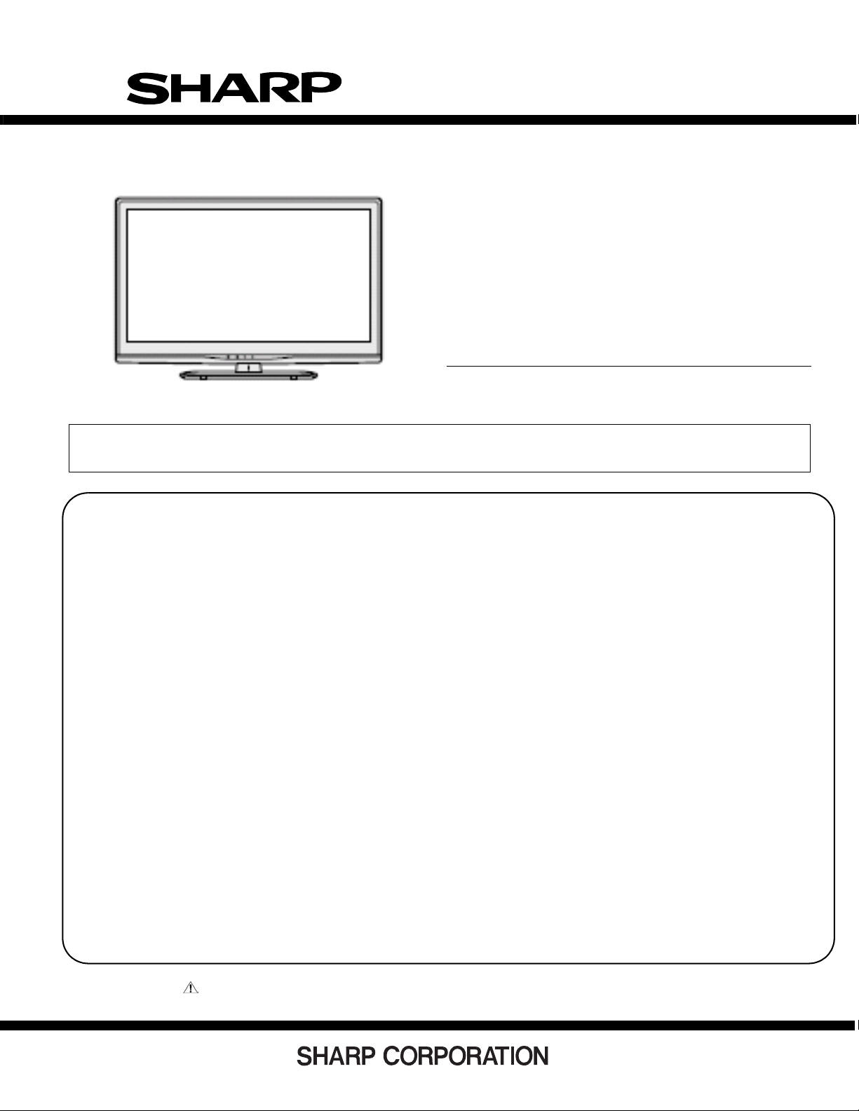
MODEL : LC-24LE150M
In the interests of user-safety (Required by safety regulations in some countries) the set should be restored to its original condition and only parts identical to those specified should be used.
CONTENTS
SAFETY PRECAUTION
IMPORTANT SERVICE SAFETY
PRECAUTION................................................i
PRECAUTION FOR USING LEAD-FREE
SOLDER.........................................................ii
CHAPTER 1. OUTLINE
[1] OUTLINE...........................................1-1
CHAPTER 2. SPECIFICATIONS
[1] SPECIFICATION.................................2-1
CHAPTER 3.OPERATION MANUAL
[1] OPERATION MANUAL........................3-1
CHAPTER 4. DIMENSIONS
[1] DIMENSIONS......................................4-1
CHAPTER 5. REMOVING OF MAJOR PARTS
[1] REMOVING OF MAJOR PARTS...........5-1
CHAPTER 6. ADJUSTMENT
[1] ADJUSTMENT....................................6-1
CHAPTER 7. TROUBLESHOOTING TABLE
[1] TROUBLESHOOTING TABLE .........................7-1
CHAPTER 8. OVERALL WIRING/BLOCK DIAGRAM
[1] SYSTEM BLOCK DIAGRAM............................8-1
CHAPTER 9. PRINTED WIRING BOARD ASSEMBLIES
[1] Main Unit .............................................9-1
[2] LED RC Unit ........................................9-5
[3] POWER Unit........................................9-7
CHAPTER 10. SCHEMATIC DIAGRAM
[1] DESCRIPTION OF SCHEMATIC
DIAGRAM ...........................................10-1
[2] MAIN Unit ...........................................10-2
[3] LED RC Unit .......................................10-4
[4] POWER Unit ......................................10-6
Parts Guide
Parts marked with " " are important for maintaining the safety of the set. Be sure to replace these parts with specified ones for maintaining the
safety and performance of the set.
This document has been published to be used for
after sales service only.
The contents are subject to change without notice.
Page 2
LC-24LE150M
SAFETY PRECAUTION
SAFETY PRECAUTIONSAFETY PRECAUTIONSAFETY PR ECAUTIONSAFETY PRECAUTIONSAFETY P RECAUTIONSAFETY PRECAUTION
LC32LE240M
IMPORTANT SERVICE SAFETY PRECAUTION
Service work should be performed only by qualified service technicians who are thoroughly familiar with all safety checks and the
servicing guidelines which follow:
5GTXKEG/CPWCN
WARNING
1. For continued safety, no modification of any circuit should be
attempted.
2. Disconnect AC power before servicing.
BEFORE RETURNING THE RECEIVER (Fire &
All checks must be repeated with the AC cord plug connection
reversed. (If necessary, a nonpolarized adaptor plug must be used
only for the purpose of completing these checks.)
Any reading of 0.74 Vrms (this corresponds to 0.5 mA rms AC.) or
more is excessive and indicates a potential shock hazard which
must be corrected before returning the monitor to the owner.
Shock Hazard)
Before returning the receiver to the user, perform the following
safety checks:
3. Inspect all lead dr ess to make certain that leads are not pinched,
and check that hardware is not lodged between the chassis and
other metal parts in the receiver.
4. Inspect all protective devices such as non-metallic control knobs,
insulation materials, cabinet backs, adjustment and compartment
covers or shields, isolation resistor-capacitor netw orks, mechanical
insulators, etc.
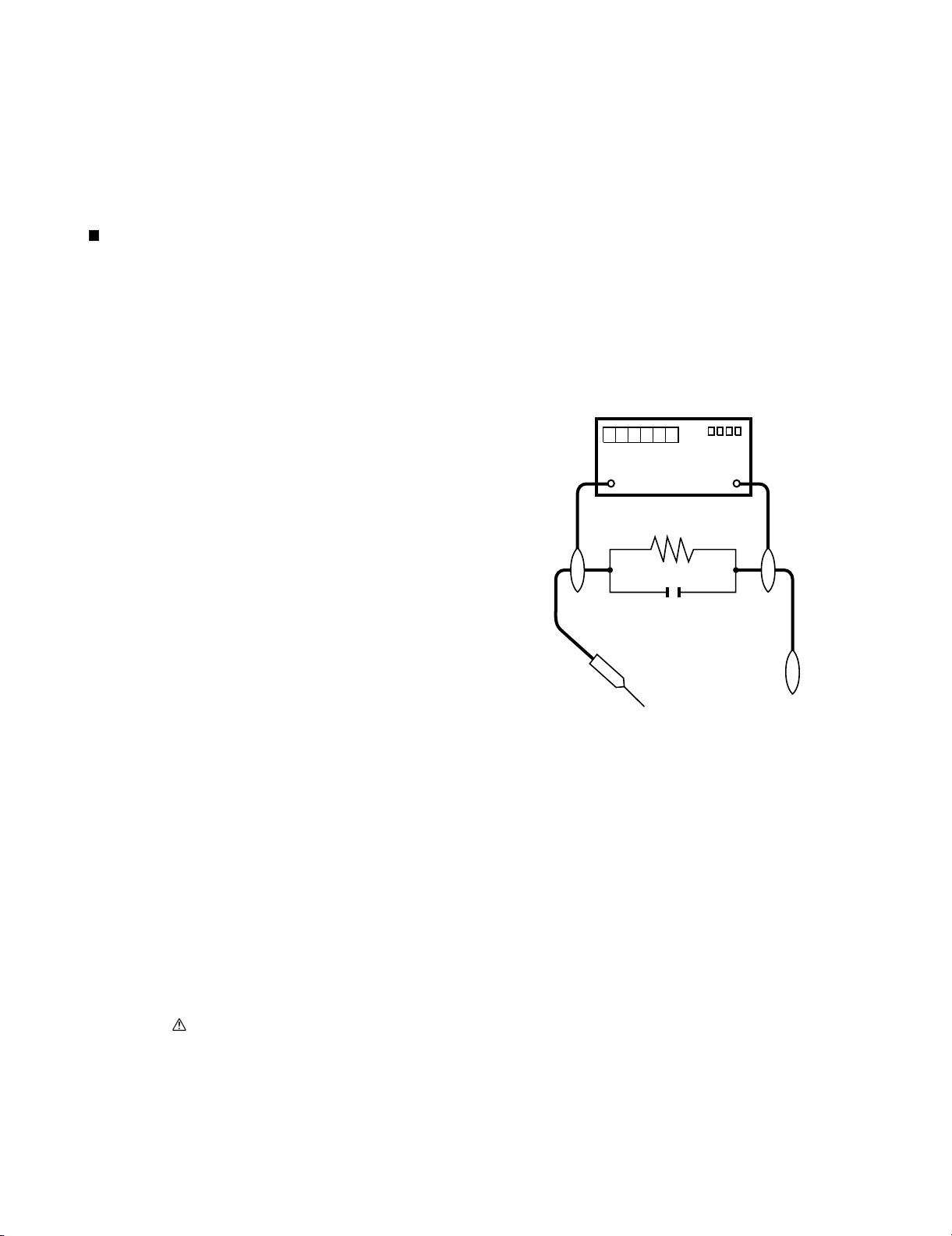
5. To be sure that no shock hazard exists, check for leakage current in
the following manner.
• Plug the AC cord directly into a 110-240 volt AC outlet.
• Using two clip leads, connect a 1.5k ohm, 10 watt resistor paralleled by a 0.15 F capacitor in series with all exposed metal cabinet
parts and a known earth ground, such as electrical conduit or electrical ground connected to an earth ground.
• Use an AC voltmeter having with 5000 ohm per volt, or higher, sensitivity or measure the AC voltage drop across the resistor.
• Connect the resistor connection to all exposed metal parts having a
return to the chassis (antenna, metal cabinet, screw heads, knobs
and control shafts, escutcheon, etc.) and measure the AC voltage
drop across the resistor.
///////////////////////////////////////////////////////////////////////////////////////////////////////////////////////////////////////////////////////////////////////////////////////////////////////////////////////////////////////////
TO EXPOSED
METAL PARTS
DVM
AC SCALE
1.5k ohm
10W
0.15µF
TEST PROBE
CONNECT TO
KNOWN EARTH
GROUND
SAFETY NOTICE
Many electrical and mechanical parts in LCD colour television have
special safety-related characteristics.
These characteristics are often not evident from visual inspection, nor
can pr otection afforded by them be necessarily increased by using
replacement components rated for higher voltage, wattage, etc.
Replacement parts which have these special safety characteristics are
identified in this manual; electrical components having such features
are identified by " " and shaded areas in the Replacement Parts List
and Schematic Diagrams.
///////////////////////////////////////////////////////////////////////////////////////////////////////////////////////////////////////////////////////////////////////////////////////////////////////////////////////////////////////////
For continued protection, replacement parts must be identical to those
used in the original circuit.
The use of a substitute replacement parts which do not have the same
safety characteristics as the factory recommended replacement parts
shown in this service manual, may create shock, fire or other hazards.
i
Page 3
LC-24LE150M
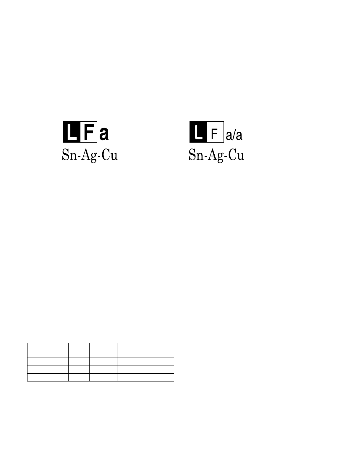
PRECAUTIONS FOR USING LEAD-FREE SOLDER
Employing lead-free solder
• “PWBs” of this model employs lead-free solder. The LF symbol indicates lead-free solder, and is attached on the PWBs and service manuals. The
alphabetical character following LF shows the type of lead-free solder.
Example:
Indicates lead-free solder of tin, silver and copper. Indicates lead-free solder of tin, silver and copper.
Using lead-free wire solder
• When fixing the PWB soldered with the lead-free solder, apply lead-free wire solder. Repairing with conventional lead wire solder may cause damage or accident due to cracks.
As the melting point of lead-free solder (Sn-Ag-Cu) is higher than the lead wire solder by 40 C, we recommend you to use a dedicated soldering
bit, if you are not familiar with how to obtain lead-free wire solder or soldering bit, contact our service station or service branch in your area.
Soldering
• As the melting point of lead-free solder (Sn-Ag-Cu) is about 220 C which is higher than the conventional lead solder by 40 C, and as it has poor
solder wettability, you may be apt to keep the soldering bit in contact with the PWB for extended period of time. However, Since the land may be
peeled off or the maximum heat-resistance temperature of parts may be exceeded, remove the bit from the PWB as soon as you confirm the
steady soldering condition.
Lead-free solder contains more tin, and the end of the soldering bit may be easily corroded. Make sure to turn on and off the power of the bit as
required.
If a different type of solder stays on the tip of the soldering bit, it is alloyed with lead-free solder. Clean the bit after every use of it.
When the tip of the soldering bit is blackened during use, file it with steel wool or fine sandpaper.
• Be careful when replacing parts with polarity indication on the PWB silk.
Lead-free wire solder for servicing
PARTS CODE
ZHNDAi123250E BL J 0.3mm 250g (1roll)
ZHNDAi126500E BK J 0.6mm 500g (1roll)
ZHNDAi12801KE BM J 1.0mm 1kg (1roll)
PRICE
RANK
PART
DELIVERY
DESCRIPTION
ii
Page 4
LC-24LE150M
T
CHAPTER 1. OUTLINE
[1] OUTLINE
MAJOR SERVICE PARTS
PWB
Ref No. Part No .
N DKEYMG260FM02
N DUNTKG255FM02
N DUNTKG265FM02
OTHER UNI
Ref No. Part No .
N RLCDTA249WJN1
ĞƐĐƌŝƉƟŽŶ
MAIN hŶŝƚ
POWER hŶŝƚ
LED RC hŶŝƚ
ĞƐĐƌŝƉƟŽŶ
24" LCD WĂŶĞů hŶŝƚ
1 – 1
Page 5
CHAPTER 2. SPECIFICATIONS
Specifications
LC-24LE150M
Item
LCD panel
Resolution
Video Colour System PAL/SECAM/NTSC 3.58/NTSC 4.43
TV
Function
Audio amplifier/Speakers
Terminals Antenna input
Power Requirement AC 110—240 V, 50/60 Hz
Power Consumption 36 W (0.8 W Standby)
Dimensions
TV-Standard PAL: B/G, D/K, I SECAM: B/G, D/K, K/K
Receiving
Channel
TV-Tuning System Auto Preset 99 ch
STEREO/BILINGUAL NICAM: B/G, I, D/K A2 stereo: B/G
INPUT 1 HDMI (HDMI input), PC input
INPUT 2 VIDEO in, AUDIO in, COMPONENT in
INPUT 3 VIDEO in, AUDIO in
OUTPUT AUDIO out, Headphone (
Model
VHF/UHF 43.25—863.25 MHz
CATV
without stand
with stand
LC-24LE150M
23.5o (598 mm) TFT LCD
1,049,088 pixels (1366 g 768)
S1—S41ch (including Hyperband)
º671:Vº671:HselgnagniweiV
5 Wg 2 / 3 g 8 cm 2pcs
UHF/VHF 75 q DIN type
3.5 mm stereo)
Vietnamese/Indonesian
561 (W) g 358 (H) g 50 (D) mm
561 (W) g 391 (H) g 178 (D) mm
561 (W)
g
423 (H)
g
178 (D) mm ( For Vietnam only )
1
NTSC: M
/iahT/naisreP/naissuR/eseugutroP/hcnerF/cibarA/esenihCdefiilpmiS/hsilgnEegaugnalDSO
)dnatshtiw(gk6.5/)dnatstuohtiw(gk2.5thgieW
Operating Temperature 0°C — 40°C
s As a part of policy of continuous improvement, SHARP reserves the right to make design and specification changes for
product improvement without prior notice. The performance specification figures indicated are nominal values of production
units. There may be some deviations from these values in individual units.
2 – 1
Page 6
LC-24LE150M
CHAPTER 3. OPERATION MANUAL
[1] OPERATION MANUAL
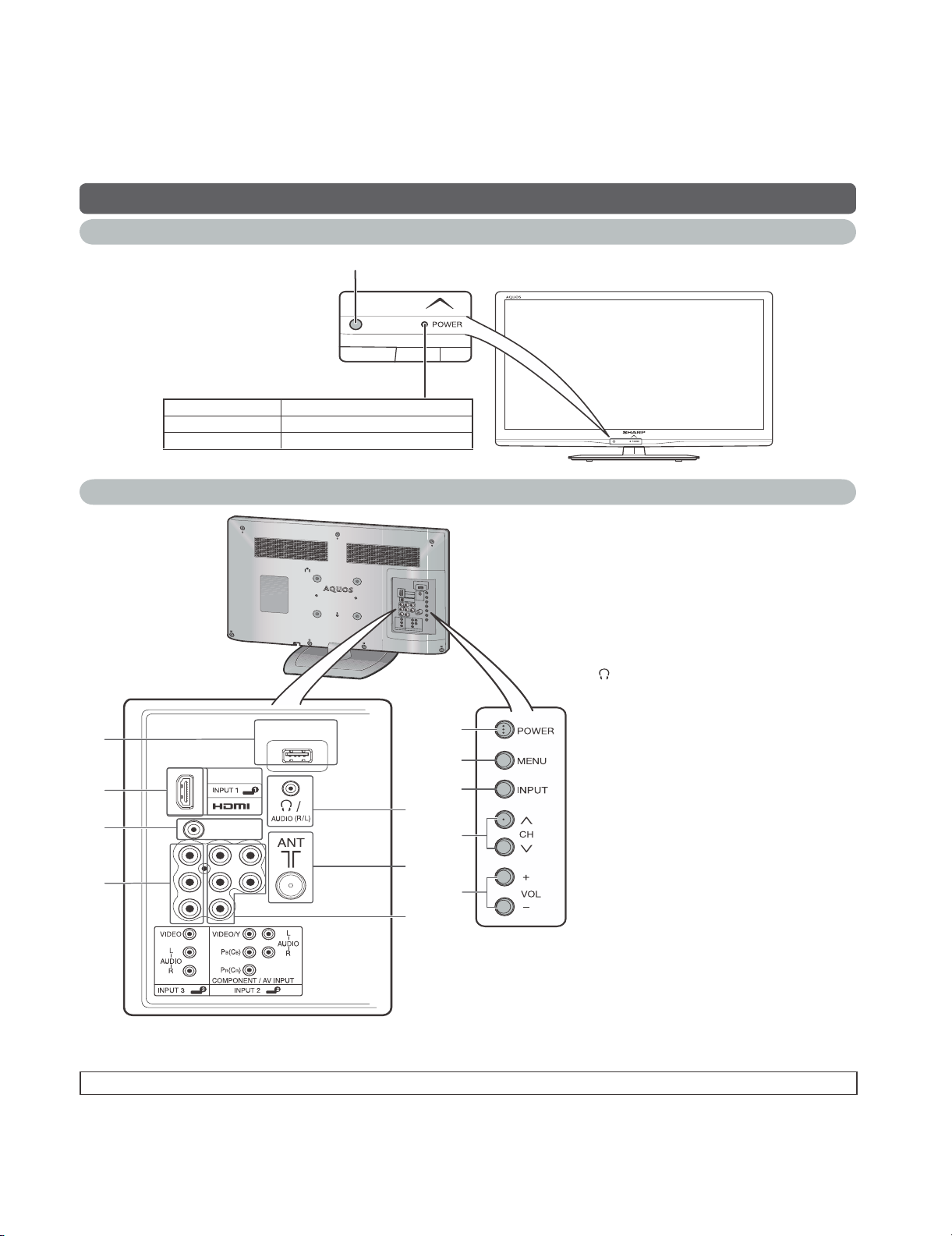
Part names
TV (Front)
Remote control sensor
POWER indicator
Light off Power off.
Lighted (Red) The TV is in standby mode.
Lighted (Green) The TV is on.
TV (Rear)
6
7
8
9
SERVICE
ONLY
SERVICEONLY
10
11
12
1 POWER (On/Off) button
2 MENU button
3 INPUT button
4 Channel up (r)/down (
5 Volume up (e)/down (f) buttons
6 SERVICE ONLY terminal*
7 INPUT 1 (HDMI) terminal
8 SERVICE ONLY terminal*
9 INPUT 3 terminals
10
/AUDIO output (R/L) terminal
11 Antenna input terminal
12 INPUT 2 (COMPONENT/AV INPUT)
1
terminals
s
) buttons
2
3
4
5
* Usually do not connect anything to this terminal as it is reserved only for service personnel.
s The illustrations in this operation manual are for explanation purposes and may vary slightly from the actual operations.
3 – 1
Page 7
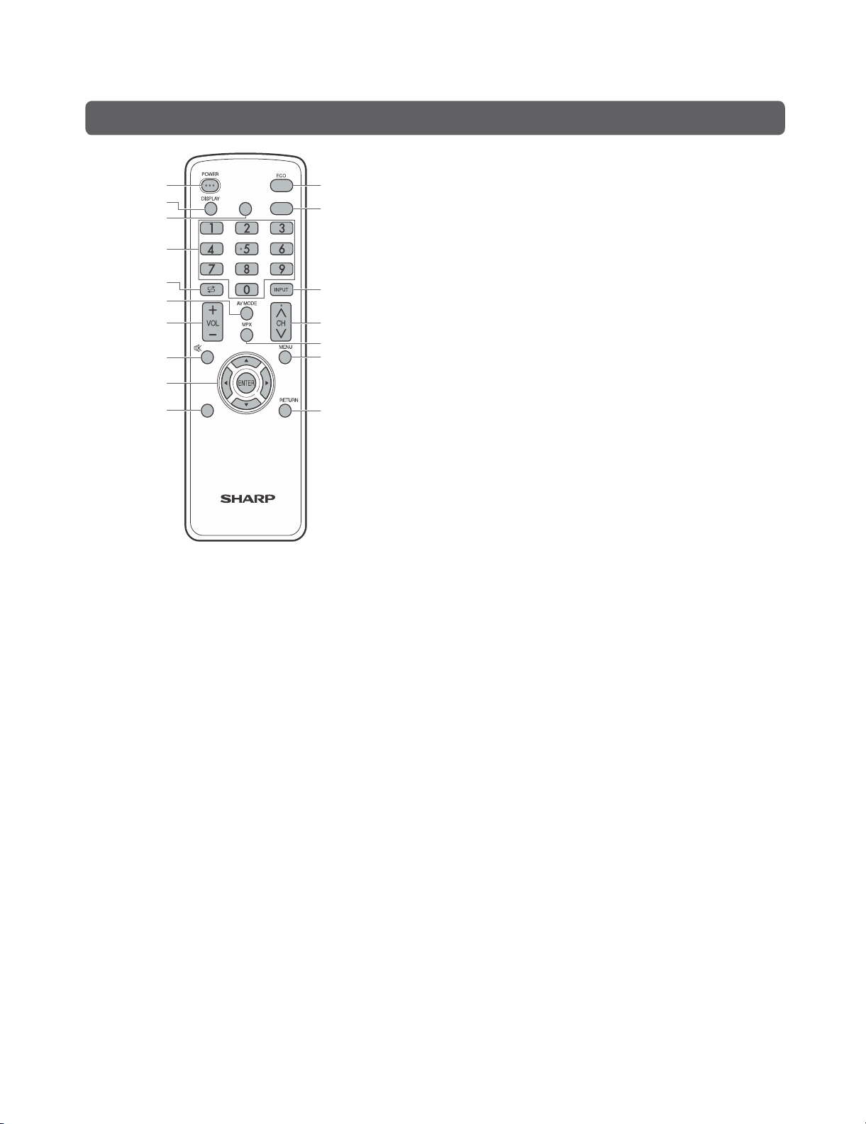
Remote control unit
LC-24LE150M
10
7 VOLk/VOL
1
2
SURROUND TIMER
3
11
12
Set the volume.
(VOLk) Increase the volume.
(VOLl) Decrease the volume.
l
8e (Mute)
e s
4
Press
Mutes sound.
Presse again s Restores sound.
5
13
6
7
14
15
8
16
9
WIDE
17
Mute will be cancelled after 30 minutes. However, the TV
will not suddenly output loud sound as the volume level will
be set to 0 automatically. Increase the volume level by
pressing VOLk.
9a/b/c/d (Cursor)
Select a desired item on the setting screen.
ENTER
Execute a command.
10 WIDE
Change the wide image mode.
11 ECO
Reduce overall power consumption based on user
LCDTV
GB095WJSA
preferences.
12 TIMER
Set the Sleep timer and Reminder.
1 POWER (STANDBY/ON)
To switch the power on and off.
2 DISPLAY
Display the channel or input information.
3 SURROUND
Select surround setting.
4 0 – 9
Set the channel.
5A (Flashback)
PressA to return to the previous selected channel
or external input mode.
6 AV MODE
Select an audio and video setting.
13 INPUT (INPUT SOURCE)
Select an input source.
14 CHr/CH
s
TV input mode: Select the channel.
(CHr) Increase the channel number.
s
) Decrease the channel number.
(CH
15 MPX
Select the sound multiplex mode.
16 MENU
Display the menu screen.
17 RETURN
MENU mode: Return to the previous menu screen.
3 – 2
Page 8
LC-24LE150M
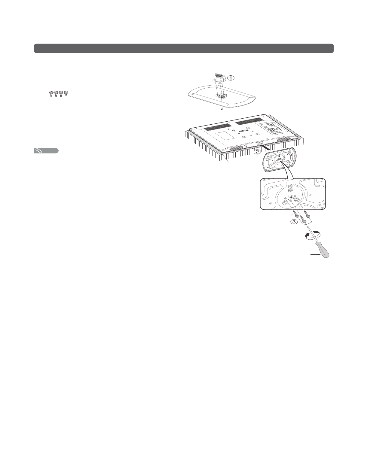
Attaching the stand
s Before attaching (or detaching) the stand, unplug the AC cord from the AC outlet.
s Before performing work spread cushioning over the base area to lay the TV on. This will prevent it from
being damaged.
Confirm the screws supplied with the TV.
1
Screws (
(used in step 1 and 3)
Insert and hook post into stand base slot holes.
2
(1)
Fix the post using short screw.
Insert the stand base to the stand post on the
3
bottom of the TV. (
Insert and tighten the 3 screws into the 3 holes
4
on the bottom of the stand base. (
NOTE
s To detach the stand, perform the steps in reverse order.
s Do not attach or detach the stand without holding it. Doing
so can cause the stand to fall, resulting in serious personal
injuries as well as damage to the stand.
4)
m
)
2
)
3
Soft cushion
Screw
Screw driver
3 – 3
Page 9
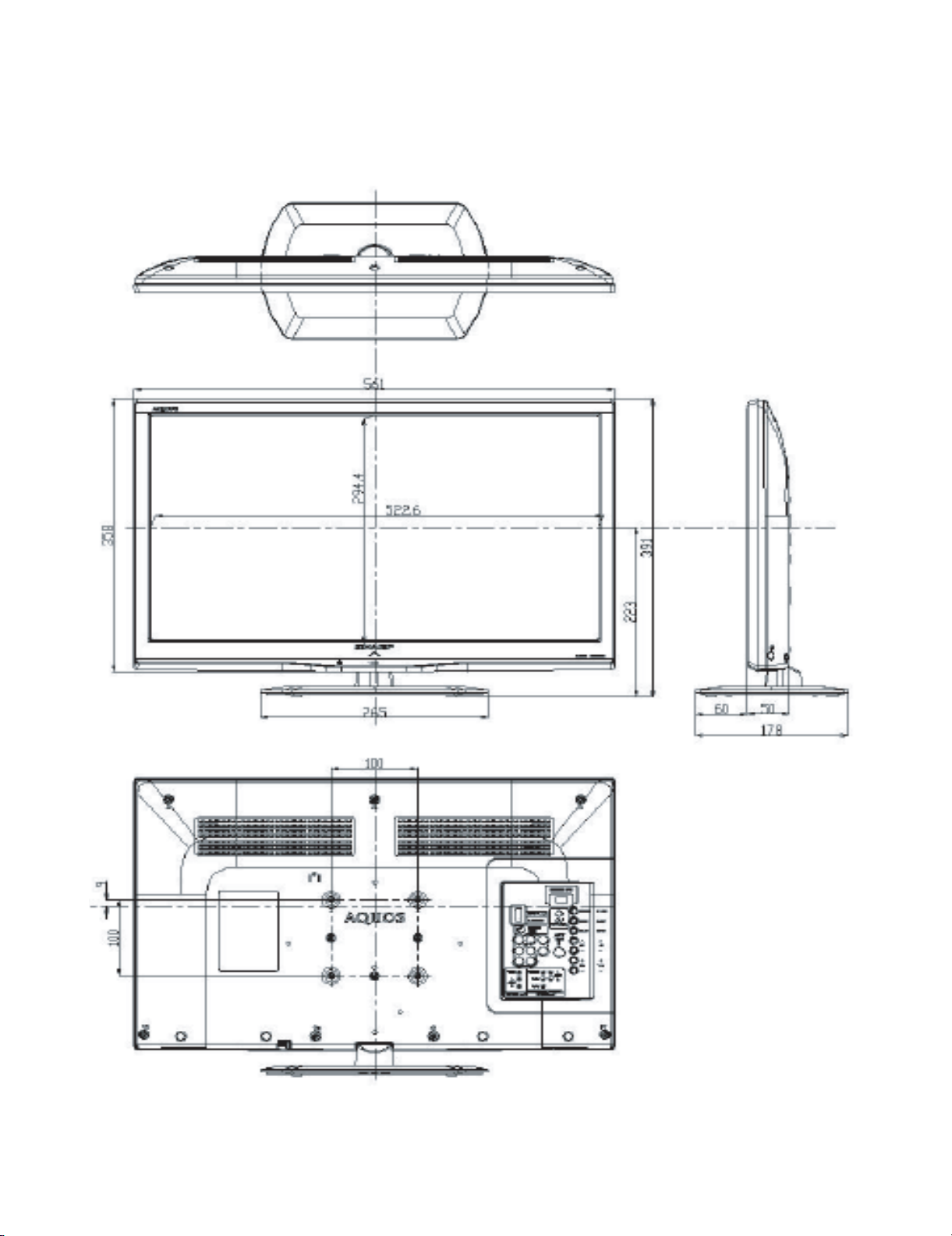
CHAPTER 4. DIMENSIONS
[1] DIMENSIONS
LC-24LE150M
[mm]
4 – 1
Page 10
LC-24LE150M
3
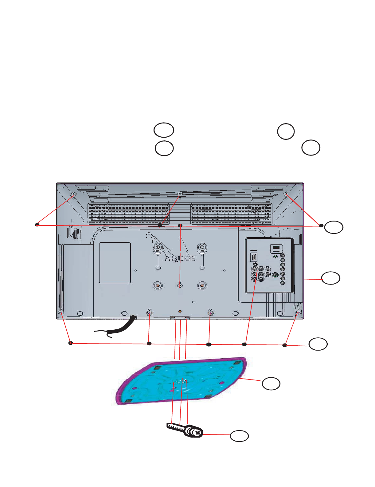
CHAPTER 5. REMOVING OF MAJOR
PARTS
[1] REMOVING OF MAJOR PARTS
[1] REMOVING OF MAJOR PARTS
1.Removing of the Rear Cabinet Ass'y and Stand Base
1 .Remove the 3 screws and detach the Stand Base
2 .Remove the 9 screws and detach the rear cabinet ass'y
1
2
4
3
4
3
2
5 – 1
Page 11
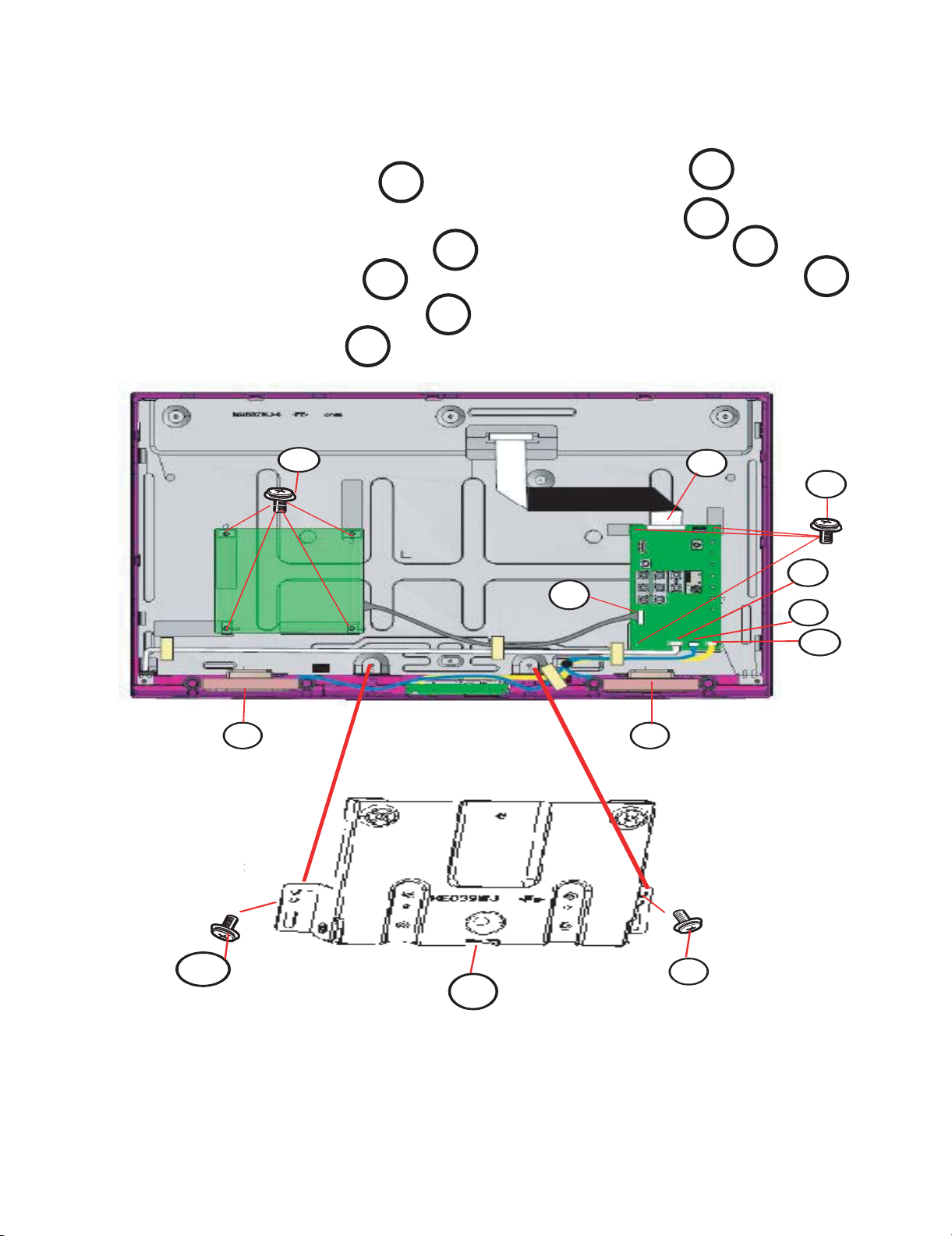
2.Removing of the Bottom Bracket & speaker L/R
5
and PWB Chassis
LC-24LE150M
1 .Remove the 2 screws and detach the bottom bracket
2 .Disconnect SP wayer & remove speaker from L/R panel bosses
3 .Disconnect LED BL FFC CABLE and disconnect LED /IR WIRE
4 .Disconnect PD wayer and remove 4 screw for remove power board
5. Disconnect LVDS FFC wayer and remove 3 screw
for remove main unit
1
4
6
8
9
6
2
3
5
8
7
9
4
1
2
5 – 2
Page 12
LC-24LE150M
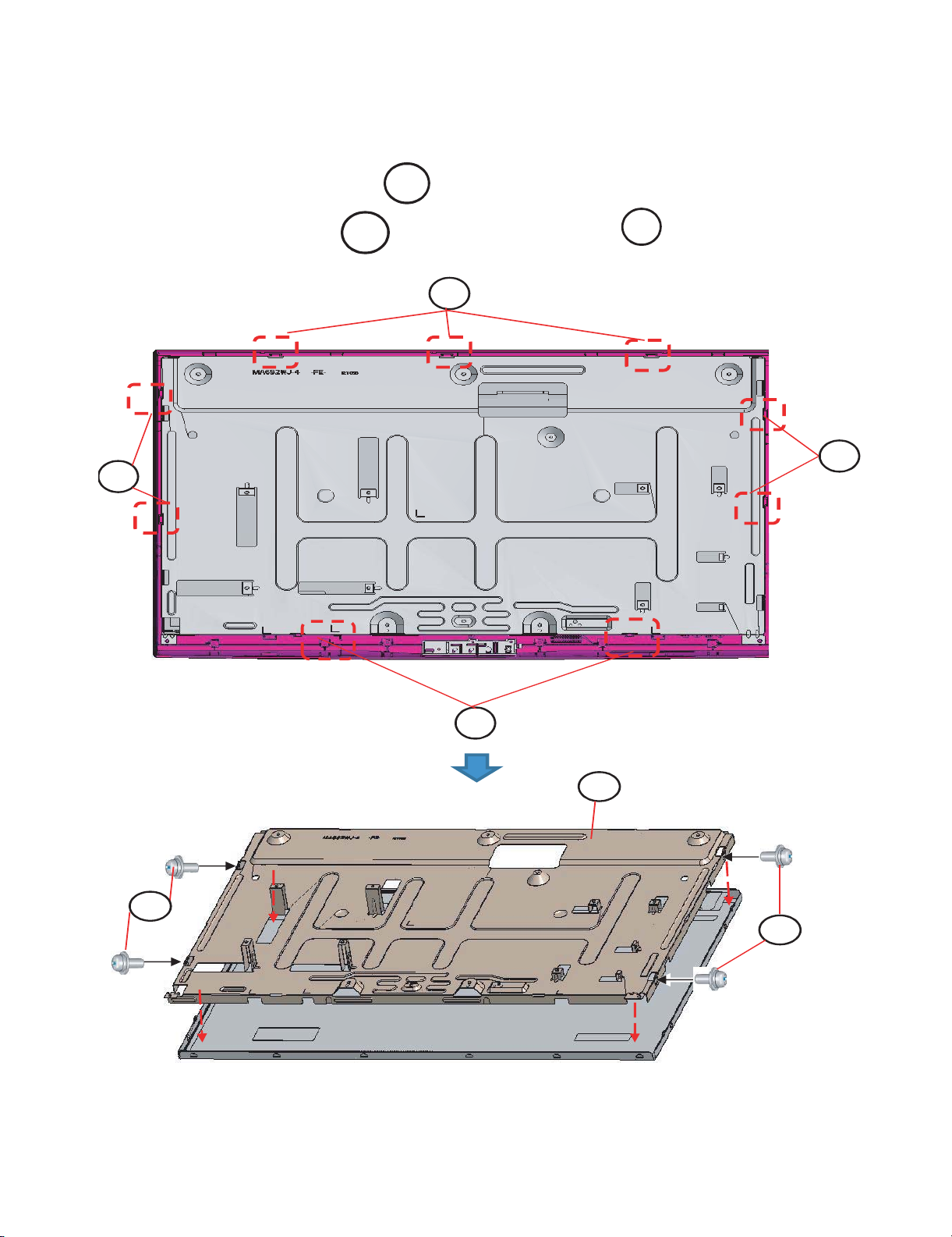
3.Removing of LCD Panel Unit
1 .Hook out the 9 lock
2.Remove 4 screw
1
1
from cab A.
2
and detech KS Tray Chassis
1
3
1
1
5 – 3
Page 13
CHAPTER 6. ADJUSTMENT
–
–
–
–
[1] ADJUSTMENT
[1]
ADJUSTMENT PROCE DURE
1.
Entering
1) While holding down the
inspec-
2) Press the Channel DOWN and Volume DOWN keys at the same time. (The
3) To cancel it, turn off the power using the Power switch or remote
2.
Remote controller
1. key
and
cancel the adjustment process mode
tion process mode is
operation
INPUT
and Volume DOWN keys at the same time, plug in the AC cord to turn on the power. (“K” standing for
displayed
key
on the upper left position of the
operation
screen.)
adjustment
control.
and
description of display in adjustment process mode.
process mode screen
LC-24LE150M
appears.)
Remote controller key
CH ( /
VOL (+ /
Cursor ( /
Cursor ( /
INPUT button on
controller
ENTER —————— ——————
* Input mode is switched
3.
Software
1) Plug off the LCD
2) Insert the USB device to the USB terminal at the LCD
(Make sure that the latest software is installed in the USB
3) Hold the LCD TV power key and plug on the LCD
4) LCD TV is on and detecting the USB
5) A few seconds later, LED light (orange) will blink indicating the software
7) T V w i l l a u t o m a t i c a l l y r e s t a r t w h e n s oftware is successfully installed
8) LCD TV is running with the latest software.
LCD TV
1. EDID DATA
–)
)
)
)
remote
upgradin
TV.
CH ( /
——————
——————
INPUT
automatically
g.
ADJUSTMENT ITEM
INPUT
Main
/+(LOV
–)
button
when relevant
device.
unit key
)
TV.
adjustment
TV.
device).
Changing
Changing
Changing
(TVÆ INPUT1 Æ INPUT2 Æ INPUT3
is started so far as the
selected line
selected line setting
egapagninruT
a selected line setting
(UP/DOWN)
(PREVIOUS/NEXT)
necessary
upgrading.
F
unc
(+1/-1)
(+10/-10)
elggot(gnihctiwsecruostupnI
switching)
)
input signal is
tion
available.
No need to input
2. SIGNAL
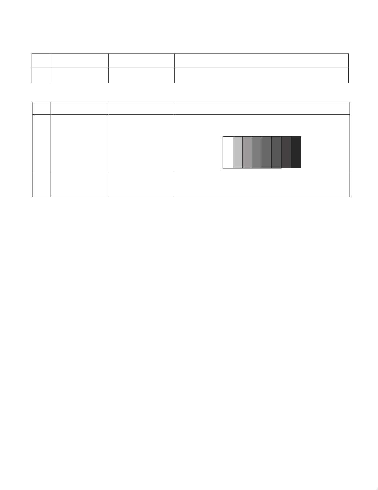
A. PICTURE
Confirmation of signal f rom generat or (setting to spec
15K Component signal ( 50Hz) Y le vel 0.7Vp- p
33K Compone nt signal Ylevel 0.7V p-p
EDID
ADJUSTMENT
ADJUSTMENT
level)
Pb, Pr level 0.7Vp-p : 0.7Vp-p
Pb, Pr level 0.7V p-p0.7Vp-p
+
p-pV7.0langisetisopmoCLAP
0.02Vp-p (pedestal to white
+
0.02Vp-p (pedestal to white
+
0.02Vp-p (pedestal to white
+
0.02Vp -p
+
0.02Vp -Com
–
level)
level)
level)
6 – 1
Page 14
LC-24LE150M
a) Adjustment
1 Adjustment Mode P ress the test key at the test remote control
b) Component 33K 60Hz Signal Adjustment (COMP-HD)
1Setting [Signal]
2 Auto Adjustment
Mode
ITEM CONDITION PROCEDURE
ITEM CONDITION PROCEDURE
COMP 3 3K 60Hz
(1080i)
100% F ull-fi eld
Bar
[Terminal]
COMPONEN T
INPUT 2
Test Mode page 5
(COMP HD)
Colour
Feed the COMPONENT 33K 60Hz (1080i) 100% Full-field
Col our B ar si gnal( 100% c olour s aturat ion) to
COMPONENT INP UT 2
100% Whit e
At the related page, move cursor to [COMP HD ADJ], press
ENTER.
[OK] appears when finished.
Black
6 – 2
Page 15
NO.
B.
WHITE BALANCE ADJUSTMENT
a) Whi te Bal ance Adjustm ent
ITEM CONDITION PROCEDURE
LC-24LE150M
i Setting Backlight : MAX
AV Mode : DYNAMIC
Active Backlight :
OFF
Set the luminance
meter on the centre
of the screen
ii Auto
Initial setting Panel Contrast
Adjustment
[command]
Adjustment
Mode
KRSW0001
KKT10037
Setting
KYOF0001
OSDS0001
SBSL0016
Multi point
adj. Mode
MSET0000
WBI20255
Point 2
WBI20204
MG2G****
MG2B****
MG2R****
Point 1
WBI10051
MG1G****
MG1B****
MG1R****
Write
MSET0003
Set
Max.Level
MGMG****
MGMR****
MGMB****
(1) Measurement MAX Brightness
(2) Set MIN Brightness
(3) Measurement HIGH Brightness
(4) Measurement LOW Brightness
(5) Calculation H Ȗ
(6) Calculation LȖ
(7) Calculation HIGH luminance (Ȗ=2.2)
(8) Calculation Initial setting of R/G/B_HIGH
(9) Set Initial setting of R/G/B_HIGH
(10) Original WB adjustment is performed (HIGH)
Set the specified gradation for point 2, fix the
most faint colour to get reference value,
adjust others 2 colours to minus adjustment for
reference value of point 2.
(11) Measurement HIGH Brightness
(Set) R_HIGH= G_HIGH
(12) Calculation MAX luminance after WB
(13) Set
(14) Calculation LOW luminance (Ȗ=2.2)
(15) Calculation Initial setting of R/G/B_LOW
(16) Set Initial setting of R/G/B_LOW
(17) Original WB adjustment is performed (LOW).
Set the specified gradation for point 1. Set G of
point 1 to the default value [(R1 x G value of
point 2/R2), with fractions rounded] and adjust
RB to the reference value of point 1.
For the details of white balance adjustment procedure, please refer to white balance
adjustment spec for Kameyama model.
1. Confirm the set condition.
2. Connect the white balance jig.
3. Through RS-232C command, adjustment mode screen is displayed.
R/G/B_MAX
R/G/B_HIGH
R/G/B_LOW
G_HIGH= G_HIGH
B_HIGH= G_HIGH
ADJ set to Ȗ=2.2 (L
R/G/B_MAX
XHG
C
nt
= 3000:1
WB
MAX
=4080
WB
H
= 3664/4080
WB
L
= 816/4080
max
=305.7 cd/m²
L
L
min=Lmax/Cnt
XH
=235.1 cd/m²
L
L
XL
=2.06 cd/m²
HȖ=LOG((L
LȖ =LOG((L
L
H22
=(L
max-Lmin
HX
=WB
WB
MAX
R_HIGH=WB
G_HIGH=WB
B_HIGH=WB
XH
XL
Example: G6 panel also use for G8/
CSOT, CMI (be careful of INT setting)
= 0.102
-L
min
)/(L
-L
min
) /(L
)x(WBH/WB
X ((L
H22
HX
’=3703
HX
’=3703
HX
’=3703
max-Lmin
max-Lmin
MAX
-L
min
)/(L
))/LOG(WBH/WB
))/LOG(WBL/WB
)^2.2+L
max-Lmin
MAX
)= 2.44
MAX
)=2.73
min
=241.31
))^(1/H Ȗ)=3703
R_HIGH=3702
G_HIGH=3641
B_HIGH=3703
RESULT
R_HIGH=3641
L
XHG=
G_HIGH=3641
231.3
B_HIGH=3641
XMX=LXHG
L
/((WBH/WB
MAX
)^2.2)=293.04
)
R_MAX=G_MAX*(R_HIGH/G_HIGH)=4078
G_MAX=WB
max-Lmin
))^(1/HȖ)=4010
MAX
X ((L
XMX
-L
min
)/(L
B_MAX=G_MAX*(B_HIGH/G_HIGH)=4078
XLX
=(L
XMX
-L
min
L
WB
LX
=WB
MAX
R_LOW=WB
G_LOW=WB
B_LOW=WB
)x(WBL/WB
X ((L
XLX
=901
XLX
=901
XLX
=901
XLX
MAX
)^2.2+L
min
-L
min
)/(L
max-Lmin
=5.08
))^(1/LȖ)=901
RESULT
R_LOW= 921
G_LOW=901
B_LOW=971
(18) Adjusted value is writing at [command]
MSET0003
6 – 3
Page 16
LC-24LE150M
(19) Set the G of point Max. to the default value
(4080 x G value of point 2 / R2). Set the R,B
Max. value [G
– G value of point 2 + (R,B
max
value of point 2)
(20) Calculate the slope R2
between MAX and Point2. R2
(R
max-Rhigh
)/(4080-3664)
slope,G2slope,B2slope
slope =
(21) Calculate the correction value پR
پG
high,پBhigh.
R
high =R2slope X
(3840-3664)
Set the reference value R,G,B of point 2
(22)
(R2’)=R2+پR
(23)
Calculate the slope R1
high
slope,G1slope,
B1
between Point2 and Point1. R1
(R
high-Rlow
(24)
Calculate the correction value پR
پG
low,پBlow.
)/(3664-816)
low,
R
low =R1slope X
(915-816)
(25)
Set the reference value R,G,B of point 1
(R1’)=R1+پR
(26) Shut down the AC power.
䯲
Initial value at RGB 2 point : 3664
䯲
Initial value at RGB 1 point : 816
[Adjustment value]
侀
Teaching set send by engineering dept is set as
reference.
low
high,
slope
slope =
[Reference values for adjustment reference]
Equipment : Luminance meter [Minolta CA-210]
Point
2 ref.
values
Point
1 ref.
values
Level
229
51
Spec
Data
x=0.272
y=0.277
x=0.272
y=0.277
Adjustment
Spec.
0.0010 0.0020
0.0045 0.0090
Inspection
Spec.
Ref. : For inspection, set the LCD TV as below.
AV MODE : [DYNAMIC] (Reset)
Aging Time : Minimum 5 minutes
6 – 4
Page 17
3.
FACTORY SETTING
AC
powerisplug
Caution:
Do not
Factory setting
Do not
off
ITEM CONDITION PROCEDURE
off
after shipment setting
plugonagain after shipment setting
with rem ote
AC
power
factory
control.
setting.
off t o
exit the
is
done.
is
done.
If do,
please r e-do
1.
Settingisdone with test remote control.
2.
Press
the
3.
When Green background appears
disappears, setting
The followings
‘Factory Setting’ key
is
completed.
are
1)
User setting
2)
Channel data (e.g. broadcast frequencies)
3)
Manufacturer’s option
4)
Password data
5)
Setting values
initialisedtofactory
are set
the
ship ment sett ing.
on the
remote control continuously.
on
screen and
setting
setti ngs
basedonmodel destination
‘K’
mark
LC-24LE150M
Model Name Factory Setting Key
A3KLE1VVZ/J/I/Y/B/N/M
A3KLE1VVP
M-Setting 100000001010110 B/G ENGLISH
P-Setting 100000001011110 M ENGLISH
Name
Remote Control Code S-System Setting OSD Language
**Please do inspection for A3KLE1VVP using NTSC signal.
Setting
6 – 5
Page 18

LC-24LE150M
CHAPTER 7. TROUBLESHOOTING
TABLE
[1] TROUBLESHOOTING TABLE
[1] TROUBLESHOOTING TABLE
No power (front LED failure to light up) or no startup (front LED failure to turn from red to green)
Is the AC cord connector tightly connected to the set? NO Reconnect the AC cord tightly and turn on the power again.
Are the wire harnesses and other cables properly connected in
YES
the set?
YES
Are the DC/DC converter outputs and the output voltages along
the control lines as specified?
1) M+5.V (IC9601)
2) D+1.1 (IC9602)
3) D+3.3V (IC9603)
4) T+ 3.3V (IC1101)
YES
Is there the AC_CTRL and PNL_POWER signal input at pins
(81 and (37) of IC3301?
YES
Check the AC CTRL signal line & PNL .Power signal line.
NO Reconnect the wire harnesses and other cables properly in the
NO Check the DC/DC converters and the control lines. Replace
NO .
set.
defective parts as required.
Check IC3301 & IC3101 and replace accordingly
7 – 1
Page 19

With [RF] signal input No video onscreen (1)
No video in the UHF/VHF reception
LC-24LE150M
Is there IF output from the tuner pin(8)(9) of TU1101 as
specified ?
Is there IF input at pin 18 & 19 of IC 3301? NO Check the circuit between TU1101 & IC3301.
Are there the LVDS signal outputs of IC3301? ( pin 43 to 52) NO Check IC3301 and its LVDS peripheral circuit.
Check LVDS cable, LCD controller (incl. panel) and their peripheral circuits.
With <Video> signal input No video onscreen (2)
No external input video onscreen <INPUT 3>
Is INPUT 3 selected on the input select menu screen?
Is there the video signal input at pin (96) of IC3301? NO Check the line between pin (7) of J501 and pin (96) of IC3301.
YES
YES
YES
YES
NO Check TU1101and its peripheral circuits.
NO Select INPUT 3 on the input select menu screen to pick up the
right input signal.
Are there LVDS signal outputs of IC3301? (pin 43 to 52) NO Check IC3301 and its LVDS peripheral circuits.
Check LVDS cable, LCD controller (incl. panel) and their peripheral circuits.
YES
YES
7 – 2
Page 20

LC-24LE150M
With <Component> signal input No video onscreen (3)
No external input video onscreen <INPUT 2>
Is INPUT 2 selected on the input select menu screen? NO Select INPUT 2 on the input select menu screen to pick up the
Are there the Y, Pb and Pr signal inputs at pins (92), (90) and
(93) of IC3301 respectively?
Is input waveform of IC3301 normal?
Y=(92) pin, Pb=(90) pin, Pr=(93) pin
Is there LVDS signal outputs of IC3301?
( pin 43 to 52 )
Check LVDS cable, LCD controller (incl. panel) and their peripheral circuits.
With <HDMI> signal input No video onscreen (4)
YES
NO Check the line between pins (10)/(11)/(12) of J501 and pins (92)/
YES
NO Check IC3301 and its peripheral circuits.
YES
NO Check IC3301 and LVDS peripheral circuits.
YES
right input signal.
(90)/(93) of IC3301.
No external input video onscreen <INPUT 1>.
right signal input.
Are there signal outputs from SC1501 to IC3301? NO Check peripheral circuits between SC1501 and IC3301.
Check LVDS cable, LCD controller (incl. panel) and their peripheral circuits.
YES
YES
YES
N(pin 43 to 52 )1033CIfostuptuolangisre LVDSehterAOCheckI
C3301 and its LVDS peripheral circuits.
ehtpukcipotneercsunemtcelestupniehtno1TUPNItceleSON?neercsunemehtnodetceles1TUPNIsI
7 – 3
Page 21

No audio heard (1)
No sound in the UHF/VHF reception.
Is the IF output from the tuner pin (8) of TU1101 as specified? NO Check TU1101 and its peripheral circuits.
YES
Is there the I2C signal input at pins (29), (30) of IC3301? NO Check IC3301 and its peripheral circuits.
YES
Is th re audio signal intput at pin(4) ,(10) of IC1701?
YES
Is the L-ch audio signal output at pin(20)(21)(23)(24) of IC3301 ? NO Check IC1701 and its peripheral circuits.
Is the R-ch audio signal output at pin(26),(27),(29),(30) of
IC1701 nor mal?
NO Check connection between IC3301 and IC1701 and its
peripheral circuits.
LC-24LE150M
YES
Are the audio signal L-ch and R-ch output at (3) /(4) and (1 ) /(2) of
P1701 normal?
YES
Check speakers and their peripheral circuits.
NO Check circuit between IC1701 & P1701.
7 – 4
Page 22

LC-24LE150M
No audio heard (2)
No external audio heard
<INPUT 2>
Is there the L-ch audio signal input from pin (4) of input terminal
TL508 to pin (47) of IC3301?
Is there the R-ch audio signal input from pin (5) of input terminal
TL510 to pin (48) of IC3301?
<INPUT 3>
Is there the L-ch audio signal input from pin (2) of input terminal
TL504 to pin (49) of IC3301?
Is there the R-ch audio signal input from pin (3) of input terminal
TL506 to pin (50) of IC3301?
YES
Is there the I2C signal input at pin (29), (30) of IC3301? NO Check IC3301 and its peripheral circuits.
YES
Is there audio signal input at pin(4),(10) of IC1701? NO Check connection between IC3301 and IC1701 and its periph-
eral circuits.
YES
Is the L-ch audio signal output at pin(20), (21) ,(23),(24) of IC3301? NO Check IC1701 and its peripheral circuits.
Is the R-ch audio signal at pin
Are the audio signal L-ch and R-ch output at (3)/(4) and (1)/(2) of
P1701 normal?
Check speakers and their peripheral circuits.
(26)(27)(29)(30) of IC1701 normal ?
YES
NO Check circuit between IC1701 & P1701.
YES
7 – 5
Page 23

No HDMI sound heard. <INPUT 1>
(*INPUT 1 is digital audio.)
LC-24LE150M
No audio heard (3)
(HDMI)”.
YES
Are waveforms input in to the pins of IC3301 normally? NO Check peripheral circuits IC3301.
ch audio signal output at pin (20),(21),(23),(30) of IC1701 normal
Is the L-
Is the R-ch audio signal output at pin(26),(27),(29),(30) of IC1701 normal
Are the audio signal L-ch and R-ch output at (3)/(4) and (1)/(2) of
P1701 normal?
Check speakers and their peripheral circuits.
YES
YES
ON4) (10) of IC1701?(niptatupnilangisoiduaerehtsI Check connection between IC3301 and IC1701 and its periph-
eral circuits.
YES
NO Check IC1701 and its peripheral circuits.
YES
NO Check circuit between IC1701 & P1701.
YES
.DIDEehtkcehCON>1TUPNI<morftuptuooiduaoN
neercsnooedivtupnilanretxeoNni>1TUPNI<“otrefeRON?neercsnoraeppaegamiIMDHehtseoD
7 – 6
Page 24

LC-24LE150M
32
"
O
N
LY
R
T
UNQA
0
73
W
JQZ
:
8
Ω
8Ω
A
C
I
R
E
SET
K
E
Y
0
UR+12
.2
V
TODC DC
CON
V
ER
T
ER
,
TU
N
ER
L
D
O
.
U
S
B, F
L
A
SH&
H
P
A
M
P
.
H
P
_IN
P151
5
P
I
N
S
LED_IRPWB
P101
5PIN
S
T
O
P
A
N
EL
K
E
Y
1
+3.3V
GPIO40
FR
O
M
C
P
U
ST
B
Y
+
5.0V
XIN
/X
O
U
T
IF+
IF
IF
_
IN
+
IF_IN
-
I2C(H
D
M
I)
clk(2)
d
a
ta(4)
H
P
D0
_
IN
H
P
M
UTE
LI
N
E
OUTL
L
IN
E
O
U
T
R
H
P
_L
H
P
_R
R
L
E
D
&
G
L
ED
CHAPTER 8. OVERALL WIRING /
BLOCK DIAGRAM
[1] SYSTEM BLOCK DIAGRAM
8 – 1
Page 25

CHAPTER 9. PRINTED WIRING
BOARD ASSEMBLIES
[1] MAIN Unit
MAIN PWB SIDE A-CHIP
H
G
LC-24LE150M
F
E
D
C
B
A
1
2 109
3
54
6
7
8
9 – 1
Page 26

LC-24LE150M
MAIN PWB SIDE A
H
G
F
E
D
C
B
A
1
2 109
3
54
6
7
8
9 – 2
Page 27

LC-24LE150M
MAIN PWB SIDE
F
MAIN PWB SIDE B-CHIP
H
G
E
D
C
B
A
1
2 109
3
54
6
7
8
9 – 3
Page 28

LC-24LE150M
F
H
G
E
D
MAIN PWB SIDE B
C
B
A
1
2 109
3
54
6
7
8
9 – 4
Page 29

[2] LED RC Unit
LED RC PWB SIDE A
LED RC PWB SIDE -A CHIP
H
G
F
LC-24LE150M
E
D
C
B
A
1
2 109
3
54
6
7
8
9 – 5
Page 30

LC-24LE150M
LED RC PWB SIDE B
LED RC PWB SIDE -B CHIP
H
G
F
E
D
C
B
A
1
2 109
3
54
6
7
8
9 – 6
Page 31

[3] POWER Unit
POWER PWB SIDE A
H
G
F
LC-24LE150M
E
D
C
B
A
1
2 109
3
54
6
7
8
9 – 7
Page 32

LC-24LE150M
POWER PWB SIDE A -CHIP
H
G
F
E
D
C
B
A
1
2 109
3
54
6
7
8
9 – 8
Page 33

LC-24LE150M
POWER PWB SIDE B
H
G
F
E
D
C
B
A
1
2 109
3
54
6
7
8
9 – 9
Page 34

LC-24LE150M
CHAPTER 10. SCHEMATIC DIA-
GRAM
[1] DESCRIPTION OF SCHEMATIC DIAGRAM
1. VOLTAG
1
)
The voltages at test point
g
enerator for ser v
EMEA
icing pur
SURE
MENT CONDITION:
s are measured on exclusive AC adaptor
pose and the above volt
2. INDICATION OF RESISTOR & C
RESISTOR
1
)The unit of re
(K=k =1000 , M=M ).
2
) All resistors are ± 5%, unless otherwi
(K= ± 10%, F= ± 1%
3
)
All
resistors are 1/16W,
C
A
P
ACITO
1)
A
l
l cap
(P=pF
2
)
All
capa
CAUTION:
T
his circuit diagram is original one
d
if
e
f
ence from your
r
SAFETY NOTES:
1
) DISCONNE
BEFORE REPLACING P
2) SEMICONDUC
POTENT
OPERA
sist
ance
""i
s omitted.
, D= ± 0.5%)
unless otherwise noted.
R
a
ci
tors
are
F
, unless oth
=
F)
.
citors are
50V
,
s.
CT THE AC PLUG
T
OR
H
IAL
SHOCK HAZARDS WHEN THE CHAS
ING
T
.
erwise
unless otherwi
therefor
,
FROM THE AC OUTLET
ART
S.
EA
T
SINKS SHOU
se noted.
noted.
se noted.
ages are measured with a 20k ohm/V tester
AP
ACITOR:
e there may b
LD BE REG
e
aslight
ARDED AS
SIS IS
and the st
able s
upply volt
age of A
.
C
110-240V
.Si
gnals are fe
dbyaco
lour
bar
signal
IMP
ORT
ANT SA
FETY NOT
A
P
R
T
S MARKED WITH "
FO
R MAINTA
REPLACE THESE PA
TAI N ING T
INING
HE SAFE
ICE:
(
"
T
HE SAFETY OF
RTS WITH SPECIFIED
T
YA
ND PERFORMA
THE S
)
ARE IMPORT
ET
.BESURETO
ONES FOR MAIN-
N
CE OFT
HE S
ANT
ET.
10 – 1
Page 35

[2] MAIN Unit
3
XIN
8
RX0
GN
4
c
c
c
c
4
LC-24LE150M
H
G
F
E
D
C
B
A
LC-24LE150M
*SC7801
NA961WJQZ
LED1K
LED2K
LED3K
LED4K
NC
VLED
VLED
NC
LED5K
LED6K
LED7K
LED8K
J506
FA068WJQZ
R
L
ZA127WJ
J501
R
Pr
L
Pb
V
Y
P9601
NB098WJ
ERR
OFL
STB
PS_ON
BL POWER
UR+13V
UR+13V
GND
GND
GND
1
2
3
4
5
6
7
8
9
10
11
12
1
2
3
4
5
6
7
8
9
10
1234
211101
321 654987
ALPACA WXGA MAIN
P101
NB150WJ
VCC
1
GND
2
IR-IN
3
LED_G
4
LED_R
5
*L7801
*D7801
@p_cod
2
*R7801
240K
*C7805
22u
*R7802
20K
*R7803
TQE
*R7804
TQE
TQE
*C7801
1000P
*C7802
*C7803
1000P
1000P
R508
6.8K
R507
6.8K
C502
470P
R50
5
R503
C501
470P
R501
R502
R504
75
R506
75
BL_ERR
OFL
STB
C9601
10u
KZA805WJQZ
C9602
47uH
PB364WJQZ
3
1
*Q7801
KU31N10D
2
3
0.2
0.2
*R7805
0.2
*C7806
1000P
*C7804
1000P
R512
C503
10K
470P
R511
10K
6.8K
C512
470P
6.8K
R509
10K
75
C3302
75
C504
5P
C505
C506
5P
R9601
100K
CY
C9603
0.1u
10u
25V
25V
*C7810
1
*R7806
15
*R7807
15
*C7809
*C7808
*C7807
1000P
1000P
1000P
COMP_R
COMP_L
AV1_R
R510
10K
AV1_L
R513
0
AV1_V
5P
100
R515
COMP_CR
R514
100
COMP_N
100
R517
COMP_CB
R51
6
100
5P
R51
9
100
COMP_Y
R51
8
100
R529
0
AV2_V
C9605
0.1u
R9602
25V
75K
CY
8
7
6
EN
RT
SS
IC9601
BD95835EFJ
BST
VIN
SW
1
2
3
R9613
82
C9620
0.1u
25V
4.7
*R7808
VCC
10u
0.1u
*C7811
5
FB
GND
4
1
BL_ERR
FAIL
2
VREG
3
4.7u
N
*C7812
4
PGND
5
*C7813
4.7u
CS
6
OVP
7
STB
STB
8
LED1
9
LED2
10
LED3
*IC
11
BD8779EF
LED4
12
LED5
13
LED6
14
LED7
15
LED8
16
*R7809
0
PWM1
17
PWM2
18
*R7810
0
PWM3
19
PWM4
20
OFL
R9603
CZ
10K
R9604
CZ
12K
F
F
R9606
56K
CZ
C9624
R9617
330P
300K
50V
CZB
C9607
10u
L9601
10uH
PB336WJQZ
*R7811
47K
AGND
40
*R7823
18K
UVLO
39
LSP
38
*R7824
120K
RT
37
*R7812
*C7816
0.47u
510
FB
36
*C7814
0.033u
SS
35
*C7815
0.47u
CP
34
VREF
33
*R7815
3
S1
32
*R7816
3
S2
31
*R7817
3
S3
7801
30
*R7818
3
S4
29
*R7819
3
S5
28
*R7820
3
S6
27
*R7821
3
S7
26
*R7822
3
S8
25
PWM8
24
*R7813
0
PWM7
23
PWM6
22
*R7814
0
PWM5
21
C9608
0.1u
25V
CKZ
8
7
EN
SS
IC9602
BD95835EFJ
BST
VIN
1
2
R9607
C9611
C9610
F
82
0.1u
10u
25V
16V
C9612
0.1u
25V
CZB
R9614
1/2W
TWF
C9609
10u
*R7831
100
*C7819
0.1u
*R7832
0
5.1K
*R7827
*C7817
1u
2.2K
*R7828
*R7833
10K
2
3
1
*J3301
JA027WJ
R3301
R3302
R3303
4.7K
C3303
R9611
100
R9605
R9612
20K
13K
F
6
5
R9609
RT
SW
3
C9615
10u
R9615
1
1
1/2W
TWF
6.2K
FB
C9621
470P
50V
GND
R9610
4
CYB
R9618
82K
CZ
L9602
10uH
PB336WJQZ
FB9602
A192WJ
1K
R1701
1
2
ON/OFF
GND
SSC
IC9603
13A1C33U
VOUT
VIN
100K
R9616
5
C9614
10u
0.047u
COMP_CB
C3304
0.047u
COMP_N
C3305
0.047u
COMP_Y
C3306
0.047u
COMP_CR
F
CY
AV1_V
0
J
AV2_V
C9626
C9617
10u
10u
C9619
10u
CZ
R1733
0
CZ
R1734
0
C9616
0.01u
CYB
3
4
R3306
10K
4.7K
4.7K
R7836
R7835
R3307
80
DGND
81
ST_GPIO_0
82
HDDC0_SDA
83
33
33
C3311
C3312
0.1u
FB3301
A192WJ
C3307
0.047u
C3308
0.047u
C3309
0.047u
R3305
2.7K
C3315
0.1u
FB3302
A192WJ
TL1701
15
16
SYNC
AVCC
17
18
1u
100u
C1701
C1702
HDDC0_SCL
84
VDDC_SDA
85
VDDC_SCL
86
ST_GPIO_5
87
ST_GPIO_6
10u
88
V10CORE
V33APLL
89
0.1u
C3313
VIN_3P
90
VIN_Y0N
91
VIN_4P
92
VIN_5P
93
GND
94
95
VN_A0N
96
VIN_9P
97
VIN_12P
TH3301
98
LSDAC3
HXA057WJQZ
99
V33VDAC
VCM_BB
1
00
V33BB1
1
C3316
0.1u
C3318
1u
C3319
C3317
0.1u
FB3304
A192WJ
1u
C1733
0
R1705
14
AM1
AM0
PVCC
PVCC
19
0.1u
C1703
C1706
330P
R1708
10
TW
C1710
0
0
0
R1712
R1707
R1710
12
11
13
10
AM2
INPL
INNL
MUTE
GND
OUTPL
BSNL
OUTNL
20
21
22
23
C1705
0.22u
C1704
1000P
L1701
L1702
22uH
22uH
PB338WJQZ
C1708
1000P
C1709
1u
R1711
R1713
10
10
TW
TW
C1707
C1711
0.1u
0.1u
100
79
2
0.1u
2.2u
C3320
AV1_L
R1715
1u
R1716
9
24
PB338WJQZ
C1712
33K
33K
R102
R103
KEY0
KEY1
10P
10P
C1501
C1502
R1502
1.5K
3.3K
R1501
R1503
4.7K
R1504
10K
KEY0
KEY1
100
100
R3309
R3308
A192WJ
FB3303
10u
10u
0.1u
C3329
C3324
C3321
78
77
76
75
HPD
AIN_3L
C3322
100K
22K
GND
BSPL
C1713
C1714
R1714
1000P
C1715
1u
74
V33IO
LSADC2
LSADC1
V10LDO
LSADC0
AIN_3R
AIN_2R
AOUT2L
AIN_2L
AOUT2R
3
4
5
6
2.2u
25
0.22u
330P
10
TW
7
2.2u
2.2u
2.2u
2.2u
C3325
C3323
C3328
C3326
0.1u
C3327
COMP_R
AV1_R
COMP_L
C1734
1u
100K
R1719
1u
1u
C1716
C1719
C1723
100K
0
R1729
R1730
8
7
6
5
4
INPR
INNR
GVDD
PLIMIT
GAIN/SLV
GND
OUTPR
GND
BSNR
OUTNR
26
27
28
29
C1717
0.22u
330P
C1718
L1704
L1703
22uH
TW
PB338WJQZ
10
R1726
C1721
1000P
C1722
1u
R1718
R1722
10
10
TW
TW
C1720
C1724
0.1u
0.1u
FB3305
1u
22uH
PB338WJQZ
1
3
S101
S102
POWER
INPUT
KA037WJ
4
2
R105
10K
R1509
100
R1508
100
D1502
47K
DB2S310L
47K
R1506
R1507
D1503
DB2S310L
20
2
1
3
22
1K
R1505
Q1501
2SC3928AR
D2P
D2N
D1P
0
0
0
0
R3344
R3345
R3346
R3347
C3331
0.1u
6.2K
R3310
73
72
71
70
69
6
REXT
RX0_GP
RX0_RN
RX0_RP
V10CORE
XOUT
V10CORE
HPOUT_R
HPOUT_L
V33BB2
8
9
10
11
12
1
0.1u
C3330
A192WJ
0.22u
C3332
HP_R
100K
R1732
3
2
FAULTZ
BSPR
30
31
C1726
0.22u
0.1u
C1729
330P
C1727
10
TW
R1723
C1725
1000P
C1728
1u
C3338
R3311
33
0.1u
10u
C3334
C3335
0.22u
C3333
1
HP_L
C3336
9P
100K
R1725
1
SDZ
IC1701
MODSEL
TPA3130
PVCC
PVCC
32
C1730
1000P
100u
C1731
R
1
R
2
L
3
L
4
1
2
3
54
6
7
8
109
10 – 2
Page 36

LC-24LE150M
KEY1
0
1u
R1501
1
7
100
ACA WXGA MAIN
SC3801
NA915WJ
1
1
1
1
1
1
1
3
3
3
3
3
56
25
MA2SD32G
Q1703
4
LVDSB_CP
V10CORE
C3347
Q1705
2SC3928AR
3
S106
KA037WJ
4
2
VOL-DOWN
R108
10K
TXA0-
A192WJ
FB3311
0.1u
C3349
55
54
53
52
LVDSA_AP
LVDSA_BN
V33LVDS
LVDSA_AN
LVDSB_EN
LVDSB_EP
LVDSA_BP
LVDSA_CN
LVDSA_CP
LVDSA_DN
LVDSA_DP
LVDSA_EN
LVDSA_EP
V10CORE
GPIO40
V10CORE
SPI_CS_N
SPI_DI
SPI_SCK
GPIO_23
DGND
GPIO_21
GPIO_18
GPIO_19
GPIO_20
GPIO_22
26
27
28
29
0.1u
R1728
4.7K
10K
R1721
S101
S102
S103
S104
POWER
INPUT
KA037WJ
4
2
33K
R103
10P
C1502
R1502
1.5K
3.3K
503
K
1504
0K
10u
C3329
75
74
LSADC2
LSADC1
AOUT2L
AOUT2R
6
7
2.2u
C3328
.
FB3305
C1734
1u
C1723
0
R1730
5
4
INPR
INNR
GND
OUTPR
28
29
L1704
22uH
C1721
1000P
C1722
1u
1722
10
TW
724
.1u
R1506
R1505
73
8
A192WJ
1u
3
30
PB338WJQZ
C1725
47K
1K
V10CORE
V33BB2
FAULTZ
BSPR
1000P
C3330
C3332
R1732
C1727
R1723
C1728
47K
R1507
Q1501
2SC3928AR
C3331
0.1u
72
9
0.1u
0.22u
HP_R
100K
2
31
C1726
0.22u
0.1u
C1729
330P
10
TW
1u
REXT
HPOUT_R
SDZ
PVCC
R105
10K
R1509
100
R1508
100
D1502
DB2S310L
D1503
DB2S310L
20
2
1
22
D2P
0
0
0
R3344
R3345
R3346
6.2K
R3310
71
70
69
RX0_GP
RX0_RN
RX0_RP
XOUT
V10CORE
HPOUT_L
10
11
12
R3311
0.1u
10u
C3334
C3335
0.22u
C3333
HP_L
C3336
9P
100K
R1725
1
IC1701
MODSEL
TPA3130
PVCC
32
C1730
1000P
100u
C1731
1
2
3
4
CH-UP
KA037WJ
KA037WJ
4
4
2
2
R106
R107
22K
68K
2
4
2
5
10
12
14
16
4
6
8
3
5
7
9
D2N
D1P
D1N
DOP
DON
0
0
0
0
R3347
R3348
R3349
R3350
68
67
66
RX0_BN
RX0_BP
RX0_GN
IC3301
IXD508WJQZ
RTD2633L
V33PLL
V10PLL
XIN
13
14
15
10u
0.1u
C3353
C3338
33
C3339
FB3306
A192WJ
FB3307
A192WJ
3
4
2
1
X3301
SCA237WJQZ
P1701
NB092WJ
Rch +
Rch -
Lch +
Lch -
18
11
13
15
17
DCLKN
DCLKP
0
R3351
FB3308
A192WJ
FB3309
A192WJ
0.1u
C3340
65
64
63
62
61
V10TMDS
RX0_CKN
RX0_CKP
V33TMDS
G33PLL
G33IFPGA
IF_N
IF_P
16
17
18
19
20
0.1u
C3343
A192WJ
FB3312
FB3313
A192WJ
0.1u
FB3310
A192WJ
C3337
10P
R1717
10K
CH-DOWN
KA037WJ
SC1501
ZA347WJQZ
19
0.1u
C3344
LVDSB_AN
V33IFADC
R1736
S105
VOL-UP
KA037WJ
4
2
21
23
60
59
58
57
LVDSB_BN
LVDSB_BP
LVDSB_CN
LVDSB_AP
U0DM
U0DP
GPIO_11
GPIO_12
21
22
23
24
10u
C3342
10u
C3346
1u
R3343
C3345
10K
C3341
0.01u
D1701
C1735
100u
R1735
0
2SA1530AR
0
1
3
S107
MENU
KA037WJ
4
2
2
R110
22K
TXA0+
51
50
49
48
47
46
45
44
43
42
NC
C3352
10u
41
C3348
0.1u
40
C3310
0.1u
39
V33IO
C3350
10u
38
C3351
0.1u
37
GPIO25
36
SPI_DO
R3335
35
4.7K
34
33
R3338
32
31
30
4.7K
R3340
10K
R1731
I2C_CLK
I2C_DAT
TXA3+
TXA3-
TXAC+
TXAC-
TXA2+
TXA2-
TXA1+
TXA1-
TXA0+
TXA0-
TXA1-
TXA1+
TXA2-
TXA2+
TXAC-
TXAC+
TXA3-
TXA3+
R3334
100
SPI_DO
D3101
TL3108
DB2S310L
SPI_CS
R3336
100
SPI_DI
R3337
100
SPI_SCK
4.7K
SPI_WP
R3101
47K
E
R1110
2.2
TWF
KTA1535T
R3105
R3102
C
Q3102
Q3101
R521
33K
R1115
2.2
C1101
TWF
4.7u
10V
C1102
B
R3103
1K
CY
R3341
10K
2SC3928AR
C517
1u
GND
2
GND
3
NC
4
SCL
5
SDA
6
GND
RXE3+
7
8
RXE3-
GND
9
10
RXEC+
11
RXEC-
12
GND
13
RXE2+
14
RXE2-
15
GND
16
RXE1+
17
RXE1-
18
GND
19
RXE0+
20
RXE0-
21
GND
22
NC
SELLVDS
23
24
GND
0
*R3801
GND
25
26
GND
27
GND
28
VCC
29
VCC
30
VCC
31
VCC
32
GND
R3807
0
R3810
100K
R3809
SCK
WP#
IN_L
IN_R
SPI_SCK
6
3
NC
NC
IC1101
3464A33N
12
R531
33K
SPI_DO
5
SI
VSS
4
1
OUT_L
IC501
TPA6139A
OUT_R
2.7K
*Q3802
C3808
KTA1535T
10u
SPI_WP
CY
R526
47K
E
R522
1K
R524
10K
Q501
2SC3928AR
R523
1K
R533
1K
4
2
3
GND
GND
C515
1u
/MUTE
VSS
5
CN
6
NC
7
CP
8
C514
1u
GND
VDD
GAIN
11
10
9
C507
1u
SDA
11
C1104
C1114
0.1u
47P
C1113
47P
100
R1106
R1108
R1109
4.7K
FB1103
FB1102
0077TA
R1107
4.7K
C1122
0.01u
B
C
Q502
KTA1535T
1K
1K
R527
R528
SCL
IF-
IF+
NC
IF-AGC
10
C1103
100
L1102
0077TA
L1101
NC
9
8
7
6
1u
C1118
C1117
5P
0.47uH
C1116
10P
C1106
0.47uH
5P
*R1101
10K
R1102
10K
C1105
10u
5
1u
L1104
0.47uH
L1103
0.47uH
*C1108
30P
*C1107
30P
R1104
1K
C1109
0.1u
Q3801
LTC014EEB
8
7
VDD
HOLD#
IC3101
M25L16M2
CE#
SO
1
2
0.1u
C3101
10K
SPI_CS
SPI_DI
4.7K
HP_L
16
15
14
HP_R
13
R1116
10K
CZ
1
2
3
GND
CE
VDD
VOUT
NC
5
4
4.7u
10V
MP(2013.04.25)
GND
4
USB_DP
3
USB_DN
2
+5V
1
J504
ZA330WJQZ
R520
470
CY
1
7
6
2
43
5
HP
J503
C513
0.1u
NC
3.3V
4
JA030WJQZ
TU1101
NQA073WJQZ
RESET
NC
3
2
1
R1112
470K
C1119
1u
10V
10u
10u
1000P
0.1u
C1110
C1112
C1111
C1115
FB1101
A191WJ
1110
12
13
14
15
16
17
18
19
10 – 3
Page 37

[3] LED RC unit
LC-24LE150M
H
LC-24LE150M
RC.LED UNIT
DUNTKG265WJZZ
G
P151
NB150WJ
TO MAIN RA
F
D+3.3V
GND
R/C
LED_G
LED_R
E
TL151
1
2
3
4
5
TL152
TL153
TL154
TL155
D
C
B
A
1
2
3
54
6
7
8
109
10 – 4
Page 38

LC-24LE150M
Green
RED
*D153
PXA194WJQZ
D152
PXA193WJQZ
R/C.LED
Q152
2SC3928AR
R154
10K
LED CONT
R158
150
0.2
R159
470
2.3
0.7
0
0
0
Q153
2SC3928AR
LED CONT
R151
100
RMC151
UA088WJ
123
C157
10u
CKZ
1.0J (2012.08.29)
C158
10u
CKZ
R152
10K
1110
12
13
14
15
16
17
18
19
10 – 5
Page 39

[4] POWER Unit
H
G
F
LC-24LE150M
E
D
C
B
A
1
2
3
54
6
7
8
109
10 – 6
Page 40

LC-24LE150M
1110
12
13
14
15
16
17
18
19
10 – 7
Page 41

PartsGuide
LC-24LE150M
PARTS GUIDE
No. S53M2024LE150M
LED BACKLIGHT TV
MODEL
LC-24LE150M
CONTENTS
[1] PRINTED WIRING BOARD
ASSEMBLIES
[2] LCD PANEL
[3] DKEYMG260FM02 (MAIN Unit)
[4] POWER UNIT
( DUNTKG255FM02 )
[5] LED / RC UNIT
( DUNTKG265FM02 )
[6] HEAT SINK ASSEMBLY
(CRDARB103WE03)
[7] HEAT SINK ASSEMBLY
(CRDARB103WE04)
[8] CABINET AND MECHNICAL
PARTS
[9] SUPPLIED ACCESSORIES
[10] PACKING PARTS ( NOT REPLACE-
MENT ITEM )
Parts marked with " " are important for maintaining the safety of the set. Be sure to replace these
parts with specified ones for maintaining the safety and performance of the set.
This document has been published to be used
for after sales service only.
The contents are subject to change without notice.
Page 42

LC-24LE150M
PRICE
NO. PARTS CODE
RANK
NEW
MARK
[1] PRINTED WIRING BOARD ASSEMBLIES
1 DKEYMG260FM02 BN V MAIN UNIT
1 DUNTKG255FM02 BD V POWER UNIT
1 DUNTKG265FM02 AV V LED/IR UNIT
[2] LCD PANEL
1 RLCDTA249WJN1 CE V LCD PANEL 24
[3] DKEYMG260FM02 (MAIN Unit)
C 0501 VCKYCY1HB471KY AA V Capacitor
C 0502 VCKYCY1HB471KY AA V Capacitor
C 0503 VCKYCY1HB471KY AA V Capacitor
C 0504 VCCCCY1HH5R0CY AB V Capacitor
C 0505 VCCCCY1HH5R0CY AB V Capacitor
C 0506 VCCCCY1HH5R0CY AA V Capacitor
C 0507 VCKYCZ1AB105KY AB V Capacitor
C 0512 VCKYCY1HB471KY AA V Capacitor
C 0513 VCKYCZ1CB104KY AA V Capacitor
C 0514 VCKYCZ1AB105KY AA V Capacitor
C 0515 VCKYCZ1AB105KY AA V Capacitor
C 0517 VCKYCY1AB105KY AB V Capacitor 1 10V Ceramic
C 1101 RC-KZA931WJQZY AB V Capacitor 4.7? 10V Ceramic
C 1102 RC-KZA931WJQZY AB V Capacitor 4.7? 10V Ceramic
C 1103 VCKYCY1AB105KY AB V Capacitor 1 10V Ceramic
C 1104 VCKYCY1CB104KY AB V Capacitor 0.1 16V Ceramic
C 1105 RC-KZA837WJQZY AA V Capacitor 10? 16V Ceramic
C 1106 VCCCCY1HH5R0CY AA V Capacitor
C 1107 VCCCCY1HH300JY AA V Capacitor
C 1108 VCCCCY1HH300JY AA V Capacitor
C 1109 VCKYCY1CB104KY AB V Capacitor 0.1 16V Ceramic
C 1110 VCKYCY1CB104KY AB V Capacitor 0.1 16V Ceramic
C 1111 RC-KZA837WJQZY AB V Capacitor 10? 16V Ceramic
C 1112 VCKYCY1HB102KY AB V Capacitor 1000p 50V Ceramic
C 1113 VCCCCY1HH470JY AB V Capacitor
C 1114 VCCCCY1HH470JY AB V Capacitor
C 1115 RC-KZA837WJQZY AB V Capacitor 10? 16V Ceramic
C 1116 VCCCCY1HH100DY AB V Capacitor
C 1117 VCCCCY1HH5R0CY AB V Capacitor
C 1118 VCKYCY1AB105KY AB V Capacitor 1 10V Ceramic
C 1119 VCKYCY1AB105KY AB V Capacitor 1 10V Ceramic
C 1122 VCKYCY1CB103KY AB V Capacitor 0.1 16V Ceramic
C 1501 VCCCCZ1HH100DY AB V Capacitor
C 1502 VCCCCZ1HH100DY AB V Capacitor
C 1701 VCEASY1EN107MY AB V Capacitor 100µ 50V Electrolitic
C 1702 RC-KZA114WJZZY AA V Capacitor 1? 10V Ceramic
C 1703 VCKYCY1EF104ZY AA V Capacitor 0.1 25V Ceramic
C 1704 VCKYCY1HB102KY AB V Capacitor 1000p 50V Ceramic
C 1705 VCKYTV1EB224KY AB V Capacitor
C 1706 VCCCCY1HH331JY AB V Capacitor
C 1707 VCKYCZ1EF104ZY AB V Capacitor
C 1708 VCKYCZ1HB102KY AB V Capacitor 1000p 50V Ceramic
C 1709 RC-KZA621WJQZY AA V Capacitor 1? 25V Ceramic
C 1710 RC-KZA114WJZZY AA V Capacitor 1? 10V Ceramic
C 1711 VCKYCZ1EF104ZY AB V Capacitor
C 1712 VCKYCZ1HB102KY AB V Capacitor 1000p 50V Ceramic
C 1713 VCKYTV1EB224KY AB V Capacitor
C 1714 VCKYCZ1HB331KY AA V Capacitor 330p 50V Ceramic
C 1715 RC-KZA621WJQZY AB V Capacitor 1? 25V Ceramic
C 1716 RC-KZA114WJZZY AB V Capacitor 1? 10V Ceramic
C 1717 VCKYTV1EB224KY AA V Capacitor
C 1718 VCKYCZ1HB331KY AB V Capacitor 330p 50V Ceramic
C 1719 RC-KZA114WJZZY AA V Capacitor 1? 10V Ceramic
C 1720 VCKYCZ1EF104ZY AA V Capacitor
C 1721 VCKYCZ1HB102KY AA V Capacitor 1000p 50V Ceramic
C 1722 RC-KZA621WJQZY AA V Capacitor 1? 25V Ceramic
C 1723 RC-KZA114WJZZY AA V Capacitor 1? 10V Ceramic
C 1724 VCKYCY1EF104ZY AB V Capacitor 0.1 25V Ceramic
C 1725 VCKYCY1HB102KY AB V Capacitor 1000p 50V Ceramic
C 1726 VCKYTV1EB224KY AA V Capacitor
C 1727 VCCCCY1HH331JY AA V Capacitor
C 1728 RC-KZA621WJQZY V Capacitor 1? 25V Ceramic
C 1729 VCKYCY1EF104ZY AA V Capacitor 0.1 25V Ceramic
C 1730 VCKYCY1HB102KY AB V Capacitor 1000p 50V Ceramic
C 1731 VCEASY1EN107MY AB V Capacitor 100µ 50V Electrolitic
C 1733 VCKYCY1AB105KY AB V Capacitor 1 10V Ceramic
C 1734 VCKYCY1AB105KY AB V Capacitor 1 10V Ceramic
C 1735 VCEASY1EN107MY AB V Capacitor 100µ 50V Electrolitic
C 3101 VCKYCY1CB104KY AB V Capacitor 0.1 16V Ceramic
C 3302 VCCCCY1HH5R0CY AB V Capacitor
C 3303 VCKYCZ1CB473KY AB V Capacitor
C 3304 VCKYCZ1CB473KY AB V Capacitor
C 3305 VCKYCY1CB473KY AB V Capacitor
C 3306 VCKYCY1CB473KY AB V Capacitor
C 3307 VCKYCZ1CB473KY AB V Capacitor
C 3308 VCKYCZ1CB473KY AB V Capacitor
C 3309 VCKYCZ1CB473KY AB V Capacitor
PART
DESCRIPTION
RANK
2
Page 43

NO. PARTS CODE
RANK
NEW
MARK
PART
RANK
DESCRIPTION
PRICE
[3] DKEYMG260FM02 (MAIN Unit)
C 3310 VCKYCZ1CB104KY AB V Capacitor
C 3311 RC-KZA837WJQZY AB V Capacitor 10? 16V Ceramic
C 3312 VCKYCY1CB104KY AB V Capacitor 0.1 16V Ceramic
C 3313 VCKYCY1CB104KY AB V Capacitor 0.1 16V Ceramic
C 3315 VCKYCY1CB104KY AB V Capacitor 0.1 16V Ceramic
C 3316 VCKYCZ1CB104KY AB V Capacitor
C 3317 VCKYCY1CB104KY AB V Capacitor 0.1 16V Ceramic
C 3318 VCKYCZ1AB105KY AB V Capacitor
C 3319 VCKYCY1CB104KY AB V Capacitor 0.1 16V Ceramic
C 3320 RC-KZA691WJZZY AB V Capacitor 2.2? 10V Ceramic
C 3321 RC-KZA837WJQZY AB V Capacitor 10? 16V Ceramic
C 3322 RC-KZA691WJZZY AB V Capacitor 2.2? 10V Ceramic
C 3323 RC-KZA691WJZZY AB V Capacitor 2.2? 10V Ceramic
C 3324 VCKYCY1CB104KY AB V Capacitor 0.1 16V Ceramic
C 3325 RC-KZA691WJZZY AB V Capacitor 2.2? 10V Ceramic
C 3326 RC-KZA691WJZZY AB V Capacitor 2.2? 10V Ceramic
C 3327 VCKYCY1CB104KY AB V Capacitor 0.1 16V Ceramic
C 3328 RC-KZA691WJZZY AB V Capacitor 2.2? 10V Ceramic
C 3329 RC-KZA837WJQZY AB V Capacitor 10? 16V Ceramic
C 3330 VCKYCY1CB104KY AB V Capacitor 0.1 16V Ceramic
C 3331 VCKYCY1CB104KY AB V Capacitor 0.1 16V Ceramic
C 3332 VCKYCY1CB224KY AB V Capacitor
C 3333 VCKYCY1CB224KY AB V Capacitor
C 3334 RC-KZA837WJQZY AB V Capacitor 10? 16V Ceramic
C 3335 VCKYCY1CB104KY AB V Capacitor 0.1 16V Ceramic
C 3336 VCCCCZ1HH9R0DY AB V Capacitor
C 3337 VCCCCZ1HH100DY AB V Capacitor
C 3338 VCKYCY1CB104KY AB V Capacitor 0.1 16V Ceramic
C 3339 VCKYCY1CB104KY AB V Capacitor 0.1 16V Ceramic
C 3340 VCKYCY1CB104KY AB V Capacitor 0.1 16V Ceramic
C 3341 VCKYCZ1CB103KY AB V Capacitor
C 3342 RC-KZA837WJQZY AB V Capacitor 10? 16V Ceramic
C 3343 VCKYCY1CB104KY AB V Capacitor 0.1 16V Ceramic
C 3344 VCKYCY1CB104KY AB V Capacitor 0.1 16V Ceramic
C 3345 VCKYCY1AB105KY AB V Capacitor 1 10V Ceramic
C 3346 RC-KZA837WJQZY AB V Capacitor 10? 16V Ceramic
C 3347 VCKYCZ1CB104KY AB V Capacitor
C 3348 VCKYCZ1CB104KY AB V Capacitor
C 3349 VCKYCY1CB104KY AB V Capacitor 0.1 16V Ceramic
C 3350 RC-KZA837WJQZY AB V Capacitor 10? 16V Ceramic
C 3351 VCKYCZ1CB104KY AB V Capacitor
C 3352 RC-KZA837WJQZY AB V Capacitor 10? 16V Ceramic
C 3353 RC-KZA837WJQZY AB V Capacitor 10? 16V Ceramic
C 3808 RC-KZA838WJQZY AB V Capacitor 10? 25V Ceramic
C 7801 VCKYCY1HB102KY AB V Capacitor 1000p 50V Ceramic
C 7802 VCKYCY1HB102KY AB V Capacitor 1000p 50V Ceramic
C 7803 VCKYCY1HB102KY AB V Capacitor 1000p 50V Ceramic
C 7804 VCKYCY1HB102KY AB V Capacitor 1000p 50V Ceramic
C 7805 VCEASY1HN226MY AB V Capacitor 22µ 50V Electrolitic
C 7806 VCKYCY1HB102KY AB V Capacitor 1000p 50V Ceramic
C 7807 VCKYCY1HB102KY AB V Capacitor 1000p 50V Ceramic
C 7808 VCKYCY1HB102KY AB V Capacitor 1000p 50V Ceramic
C 7809 VCKYCY1HB102KY AB V Capacitor 1000p 50V Ceramic
C 7810 VCKYCY1CB104KY AB V Capacitor 0.1 16V Ceramic
C 7811 RC-KZA838WJQZY AB V Capacitor 10? 25V Ceramic
C 7812 RC-KZA213WJZZY AB V Capacitor 4.7? 10V Ceramic
C 7813 RC-KZA213WJZZY AB V Capacitor 4.7? 10V Ceramic
C 7814 VCKYCY1HB333KY AB V Capacitor
C 7815 VCKYTV1EB474KY AB V Capacitor
C 7816 VCKYTV1EB474KY AB V Capacitor
C 7817 VCKYCY1AB105KY AB V Capacitor 1 10V Ceramic
C 7819 VCKYCY1CB104KY AB V Capacitor 0.1 16V Ceramic
C 9601 RC-KZA805WJQZY AB V Capacitor 10? 25V Ceramic
C 9602 RC-KZA806WJQZY AB V Capacitor 0.1? 25V Ceramic
C 9603 RC-KZA838WJQZY AA V Capacitor 10? 25V Ceramic
C 9605 RC-KZA806WJQZY AA V Capacitor 0.1? 25V Ceramic
C 9607 RC-KZA837WJQZY AA V Capacitor 10? 16V Ceramic
C 9608 RC-KZA806WJQZY AB V Capacitor 0.1? 25V Ceramic
C 9609 RC-KZA837WJQZY AB V Capacitor 10? 16V Ceramic
C 9610 RC-KZA837WJQZY AB V Capacitor 10? 16V Ceramic
C 9611 VCKYCY1EB104KY AB V Capacitor 0.1 25V Ceramic
C 9612 VCKYCZ1EB104KY AB V Capacitor
C 9614 RC-KZA837WJQZY AB V Capacitor 10? 16V Ceramic
C 9615 RC-KZA837WJQZY AB V Capacitor 10? 16V Ceramic
C 9616 VCKYCY1EB103KY AB V Capacitor
C 9617 RC-KZA837WJQZY AB V Capacitor 10? 16V Ceramic
C 9619 RC-KZA837WJQZY AB V Capacitor 10? 16V Ceramic
C 9620 VCKYCZ1EB104KY AB V Capacitor
C 9621 VCKYCY1HB471KY AB V Capacitor
C 9624 VCKYCZ1HB331KY AB V Capacitor 330p 50V Ceramic
C 9626 RC-KZA837WJQZY AB V Capacitor 10? 16V Ceramic
D 1502 VHDDB2S310L-1Y AA V Diode
D 1503 VHDDB2S310L-1Y AA V Diode
D 1701 VHDPMEG3002-1Y AA V Diode
D 3101 VHDDB2S310L-1Y AA V Diode
LC-24LE150M
3
Page 44

LC-24LE150M
PRICE
NO. PARTS CODE
RANK
NEW
MARK
[3] DKEYMG260FM02 (MAIN Unit)
D 7801 VHDMBRD6U60-1Y AA V Diode
FB 1101 RBLN-A191WJZZY AB V Ferrite Bead
FB 1102 RBLN-0077TAZZY AB V Ferrite Bead
FB 1103 RBLN-0077TAZZY AB V Ferrite Bead
FB 3301 RBLN-A192WJZZY AB V Ferrite Bead
FB 3302 RBLN-A192WJZZY AB V Ferrite Bead
FB 3303 RBLN-A192WJZZY AB V Ferrite Bead
FB 3304 RBLN-A192WJZZY AB V Ferrite Bead
FB 3305 RBLN-A192WJZZY AB V Ferrite Bead
FB 3306 RBLN-A192WJZZY AB V Ferrite Bead
FB 3307 RBLN-A192WJZZY AB V Ferrite Bead
FB 3308 RBLN-A192WJZZY AB V Ferrite Bead
FB 3309 RBLN-A192WJZZY AB V Ferrite Bead
FB 3310 RBLN-A192WJZZY AB V Ferrite Bead
FB 3311 RBLN-A192WJZZY AB V Ferrite Bead
FB 3312 RBLN-A192WJZZY AB V Ferrite Bead
FB 3313 RBLN-A192WJZZY AB V Ferrite Bead
FB 9602 RBLN-A192WJZZY AB V Ferrite Bead
IC 0501 VHITPA6139A-1Y AF V IC
IC 1101 VHI3464A33N-1Y V IC
IC 1701 VHITPA3130D-1Y AL V IC
IC 3101 VHIEN25QH16-1Y V IC
IC 3301 RH-IXD508WJQZQ V IC
IC 7801 VHIBD8779EF-1Y V IC
IC 9601 VHIBD95835E-1Y V IC
IC 9602 VHIBD95835E-1Y V IC
IC 9603 VHI13A1C33U-1Y V IC
J 0501 QJAKZA127WJZZ AC V Jack
J 0503 QJAKJA030WJQZ AD V Jack
J 0504 QSOCZA330WJQZ AD V USB Socket
J 0506 QJAKFA068WJQZ AG V Jack
J 3301 QJAKJA027WJZZ AD V Jack
L 1101 VPMTNR47JR65NY AD V Coil
L 1102 VPMTNR47JR65NY AD V Coil
L 1103 VPMTNR47JR65NY AD V Coil
L 1104 VPMTNR47JR65NY AD V Coil
L 1701 RCILPB338WJQZY AD V Coil
L 1702 RCILPB338WJQZY AD V Coil
L 1703 RCILPB338WJQZY AD V Coil
L 1704 RCILPB338WJQZY AD V Coil
L 7801 RCILPB364WJQZY AD V Coil
L 9601 RCILPB336WJQZY AD V Coil
L 9602 RCILPB336WJQZY AD V Coil
P 0101 QPLGNB150WJZZY AC V LED IR Socket
P 1701 QPLGNB092WJZZY AD V SP Socket
P 9601 QPLGNB098WJZZY AC V PD Socket
Q 0501 VS2SC3928AR-1Y AB V Transistor 2SC3928A-T112V-1R
Q 0502 VSKTA1535T+-1Y AC V Transistor KTA1535T-RTK/P
Q 1501 VS2SC3928AR-1Y AB V Transistor 2SC3928A-T112V-1R
Q 1703 VSISA1530AC-1Y AB V Transistor ISA1530AC-T112V-1R
Q 1705 VS2SC3928AR-1Y AB V Transistor 2SC3928A-T112V-1R
Q 3101 VS2SC3928AR-1Y AB V Transistor 2SC3928A-T112V-1R
Q 3102 VSKTA1535T+-1Y AC V Transistor KTA1535T-RTK/P
Q 3801 VSKRC102S//-1Y AB V Transistor KRC1025-RTK/P
Q 3802 VSKTA1535T+-1Y AB V Transistor KTA1535T-RTK/P
Q 7801 VSKU310N10D-1Y V Transistor
R 0102 VRS-CZ1JF333JY AA V Resistor 3.3k 1/16w Metal Oxide
R 0103 VRS-CZ1JF333JY AA V Resistor 3.3k 1/16w Metal Oxide
R 0105 VRS-CZ1JF103JY AA V Resistor 10k 1/16w Metal Oxide
R 0106 VRS-CZ1JF223JY AA V Resistor 22k 1/16w Metal Oxide
R 0107 VRS-CZ1JF683JY AA V Resistor 68k 1/16w Metal Oxide
R 0108 VRS-CZ1JF103JY AA V Resistor 10k 1/16w Metal Oxide
R 0110 VRS-CZ1JF223JY AA V Resistor 22k 1/16w Metal Oxide
R 0501 VRS-TQ2EF750JY AA V Resistor 75 1/4w Metal Oxide
R 0502 VRS-TQ2EF750JY AA V Resistor 75 1/4w Metal Oxide
R 0503 VRS-CY1JF682JY AA V Resistor 68k 1/16w Metal Oxide
R 0504 VRS-TQ2EF750JY AA V Resistor 75 1/4w Metal Oxide
R 0505 VRS-CY1JF682JY AA V Resistor 68k 1/16w Metal Oxide
R 0506 VRS-TQ2EF750JY AA V Resistor 75 1/4w Metal Oxide
R 0507 VRS-CY1JF682JY AA V Resistor 68k 1/16w Metal Oxide
R 0508 VRS-CY1JF682JY AA V Resistor 68k 1/16w Metal Oxide
R 0509 VRS-CY1JF103JY AA V Resistor 10k 1/16w Metal Oxide
R 0510 VRS-CY1JF103JY AA V Resistor 10k 1/16w Metal Oxide
R 0511 VRS-CY1JF103JY AA V Resistor 10k 1/16w Metal Oxide
R 0512 VRS-CY1JF103JY AA V Resistor 10k 1/16w Metal Oxide
R 0513 VRS-CY1JF000JY AA V Resistor 0 1/16w Metal Oxide
R 0514 VRS-CZ1JF101JY AA V Resistor 100 1/16w Metal Oxide
R 0515 VRS-CZ1JF101JY AA V Resistor 100 1/16w Metal Oxide
R 0516 VRS-CZ1JF101JY AA V Resistor 100 1/16w Metal Oxide
R 0517 VRS-CZ1JF101JY AA V Resistor 100 1/16w Metal Oxide
R 0518 VRS-CZ1JF101JY AA V Resistor 100 1/16w Metal Oxide
R 0519 VRS-CZ1JF101JY AA V Resistor 100 1/16w Metal Oxide
R 0520 VRS-CY1JF471JY AA V Resistor 470 1/16w Metal Oxide
R 0521 VRS-CZ1JF333JY AA V Resistor 3.3k 1/16w Metal Oxide
R 0522 VRS-CY1JF102JY AA V Resistor 1k 1/16w Metal Oxide
PART
DESCRIPTION
RANK
4
Page 45

NO. PARTS CODE
RANK
NEW
MARK
PART
RANK
DESCRIPTION
PRICE
[3] DKEYMG260FM02 (MAIN Unit)
R 0523 VRS-CZ1JF102JY AA V Resistor 1k 1/16w Metal Oxide
R 0524 VRS-CY1JF103JY AA V Resistor 10k 1/16w Metal Oxide
R 0526 VRS-CY1JF473JY AA V Resistor 47k 1/16w Metal Oxide
R 0527 VRS-CZ1JF102JY AA V Resistor 1k 1/16w Metal Oxide
R 0528 VRS-CZ1JF102JY AA V Resistor 1k 1/16w Metal Oxide
R 0529 VRS-CZ1JF000JY AA V Resistor 0 1/16w Metal Oxide
R 0531 VRS-CZ1JF333JY AA V Resistor 3.3k 1/16w Metal Oxide
R 0533 VRS-CZ1JF102JY AA V Resistor 1k 1/16w Metal Oxide
R 1101 VRS-CY1JF103JY AA V Resistor 10k 1/16w Metal Oxide
R 1102 VRS-CY1JF103JY AA V Resistor 10k 1/16w Metal Oxide
R 1104 VRS-CY1JF102JY AA V Resistor 1k 1/16w Metal Oxide
R 1106 VRS-CY1JF101JY AA V Resistor 100 1/16w Metal Oxide
R 1107 VRS-CY1JF472JY AA V Resistor 4.7k 1/16w Metal Oxide
R 1108 VRS-CY1JF101JY AA V Resistor 100 1/16w Metal Oxide
R 1109 VRS-CY1JF472JY AA V Resistor 4.7k 1/16w Metal Oxide
R 1110 VRS-TW2HF2R2JY AA V Resistor
R 1112 VRS-CY1JF474JY AA V Resistor 470k 1/16w Metal Oxide
R 1115 VRS-TW2HF2R2JY AA V Resistor
R 1116 VRS-CZ1JF103JY AA V Resistor 10k 1/16w Metal Oxide
R 1501 VRS-CZ1JF332JY AA V Resistor 3.3k 1/16w Metal Oxide
R 1502 VRS-CZ1JF152JY AA V Resistor 1.5k 1/16w Metal Oxide
R 1503 VRS-CZ1JF472JY AA V Resistor 4.7k 1/16w Metal Oxide
R 1504 VRS-CZ1JF103JY AA V Resistor 10k 1/16w Metal Oxide
R 1505 VRS-CZ1JF102JY AA V Resistor 1k 1/16w Metal Oxide
R 1506 VRS-CZ1JF473JY AA V Resistor 47k 1/16w Metal Oxide
R 1507 VRS-CZ1JF473JY AA V Resistor 47k 1/16w Metal Oxide
R 1508 VRS-CZ1JF101JY AA V Resistor 100 1/16w Metal Oxide
R 1509 VRS-CZ1JF101JY AA V Resistor 100 1/16w Metal Oxide
R 1701 VRS-CY1JF472JY AA V Resistor 4.7k 1/16w Metal Oxide
R 1705 VRS-CY1JF000JY AA V Resistor 0 1/16w Metal Oxide
R 1707 VRS-CY1JF000JY AA V Resistor 0 1/16w Metal Oxide
R 1708 VRS-TW2ED100JY AA V Resistor
R 1710 VRS-CY1JF000JY AA V Resistor 0 1/16w Metal Oxide
R 1711 VRS-TW2ED100JY AA V Resistor
R 1712 VRS-CY1JF000JY AA V Resistor 0 1/16w Metal Oxide
R 1713 VRS-TW2ED100JY AA V Resistor
R 1714 VRS-TW2ED100JY AA V Resistor
R 1715 VRS-CY1JF104JY AA V Resistor 100k 1/16w Metal Oxide
R 1716 VRS-CY1JF223JY AA V Resistor 22k 1/16w Metal Oxide
R 1717 VRS-CY1JF103JY AA V Resistor 10k 1/16w Metal Oxide
R 1718 VRS-TW2ED100JY AA V Resistor
R 1719 VRS-CY1JF104JY AA V Resistor 100k 1/16w Metal Oxide
R 1721 VRS-CY1JF103JY AA V Resistor 10k 1/16w Metal Oxide
R 1722 VRS-TW2ED100JY AA V Resistor
R 1723 VRS-TW2ED100JY AA V Resistor
R 1725 VRS-CY1JF104JY AA V Resistor 100k 1/16w Metal Oxide
R 1726 VRS-TW2ED100JY AA V Resistor
R 1728 VRS-CY1JF472JY AA V Resistor 4.7k 1/16w Metal Oxide
R 1729 VRS-CY1JF104JY AA V Resistor 100k 1/16w Metal Oxide
R 1730 VRS-CY1JF000JY AA V Resistor 0 1/16w Metal Oxide
R 1731 VRS-CZ1JF103JY AA V Resistor 10k 1/16w Metal Oxide
R 1732 VRS-CZ1JF104JY AA V Resistor 100k 1/16w Metal Oxide
R 1733 VRS-CZ1JF000JY AA V Resistor 0 1/16w Metal Oxide
R 1734 VRS-CZ1JF000JY AA V Resistor 0 1/16w Metal Oxide
R 1735 VRS-CY1JF000JY AA V Resistor 0 1/16w Metal Oxide
R 1736 VRS-CY1JF000JY AA V Resistor 0 1/16w Metal Oxide
R 3101 VRS-CY1JF473JY AA V Resistor 47k 1/16w Metal Oxide
R 3102 VRS-CY1JF472JY AA V Resistor 4.7k 1/16w Metal Oxide
R 3103 VRS-CY1JF102JY AA V Resistor 1k 1/16w Metal Oxide
R 3105 VRS-CZ1JF273JY AA V Resistor 27k 1/16w Metal Oxide
R 3301 VRS-CZ1JF330JY AA V Resistor 33 1/16w Metal Oxide
R 3302 VRS-CZ1JF330JY AA V Resistor 33 1/16w Metal Oxide
R 3303 VRS-CZ1JF472JY AA V Resistor 4.7k 1/16w Metal Oxide
R 3305 VRS-CZ1JF272JY AA V Resistor 2.7k 1/16w Metal Oxide
R 3306 VRS-CZ1JF103JY AA V Resistor 10k 1/16w Metal Oxide
R 3307 VRS-CZ1JF101JY AA V Resistor 100 1/16w Metal Oxide
R 3308 VRS-CZ1JF101JY AA V Resistor 100 1/16w Metal Oxide
R 3309 VRS-CZ1JF101JY AA V Resistor 100 1/16w Metal Oxide
R 3310 VRS-CZ1JF622JY AA V Resistor 6.2k 1/16w Metal Oxide
R 3311 VRS-CZ1JF330JY AA V Resistor 33 1/16w Metal Oxide
R 3334 VRS-CZ1JF101JY AA V Resistor 100 1/16w Metal Oxide
R 3335 VRS-CZ1JF472JY AA V Resistor 4.7k 1/16w Metal Oxide
R 3336 VRS-CZ1JF101JY AA V Resistor 100 1/16w Metal Oxide
R 3337 VRS-CZ1JF101JY AA V Resistor 100 1/16w Metal Oxide
R 3338 VRS-CZ1JF472JY AA V Resistor 4.7k 1/16w Metal Oxide
R 3340 VRS-CZ1JF472JY AA V Resistor 4.7k 1/16w Metal Oxide
R 3341 VRS-CZ1JF103JY AA V Resistor 10k 1/16w Metal Oxide
R 3343 VRS-CZ1JF103JY AA V Resistor 10k 1/16w Metal Oxide
R 3344 VRS-CZ1JF000JY AA V Resistor 0 1/16w Metal Oxide
R 3345 VRS-CZ1JF000JY AA V Resistor 0 1/16w Metal Oxide
R 3346 VRS-CZ1JF000JY AA V Resistor 0 1/16w Metal Oxide
R 3347 VRS-CZ1JF000JY AA V Resistor 0 1/16w Metal Oxide
R 3348 VRS-CZ1JF000JY AA V Resistor 0 1/16w Metal Oxide
R 3349 VRS-CZ1JF000JY AA V Resistor 0 1/16w Metal Oxide
R 3350 VRS-CZ1JF000JY AA V Resistor 0 1/16w Metal Oxide
LC-24LE150M
5
Page 46

LC-24LE150M
PRICE
NO. PARTS CODE
RANK
NEW
MARK
[3] DKEYMG260FM02 (MAIN Unit)
R 3351 VRS-CZ1JF000JY AA V Resistor 0 1/16w Metal Oxide
R 3801 VRS-CZ1JF000JY AA V Resistor 0 1/16w Metal Oxide
R 3807 VRS-CY1JF000JY AA V Resistor 0 1/16w Metal Oxide
R 3809 VRS-CY1JF272JY AA V Resistor 2.7k 1/16w Metal Oxide
R 3810 VRS-CY1JF104JY AA V Resistor 100k 1/16w Metal Oxide
R 7801 VRS-CY1JF244JY AA V Resistor 240k 1/16w Metal Oxide
R 7802 VRS-CY1JF203JY AA V Resistor 20k 1/16w Metal Oxide
R 7803 VRS-TQ2EDR20FY AA V Resistor 20 1/4w Metal Oxide
R 7804 VRS-TQ2EDR20FY AA V Resistor 20 1/4w Metal Oxide
R 7805 VRS-TQ2EDR20FY AA V Resistor 20 1/4w Metal Oxide
R 7806 VRS-TW2HF150JY AA V Resistor
R 7807 VRS-TW2HF150JY AA V Resistor
R 7808 VRS-TW2ED4R7JY AA V Resistor
R 7809 VRS-CY1JF000JY AA V Resistor 0 1/16w Metal Oxide
R 7810 VRS-CY1JF000JY AA V Resistor 0 1/16w Metal Oxide
R 7811 VRS-CY1JF473JY AA V Resistor 47k 1/16w Metal Oxide
R 7812 VRS-CY1JF511JY AA V Resistor 510 1/16w Metal Oxide
R 7813 VRS-CY1JF000JY AA V Resistor 0 1/16w Metal Oxide
R 7814 VRS-CY1JF000JY AA V Resistor 0 1/16w Metal Oxide
R 7815 VRS-TW2ED3R0JY AA V Resistor
R 7816 VRS-TW2ED3R0JY AA V Resistor
R 7817 VRS-TW2ED3R0JY AA V Resistor
R 7818 VRS-TW2ED3R0JY AA V Resistor
R 7819 VRS-TW2ED3R0JY AA V Resistor
R 7820 VRS-TW2ED3R0JY AA V Resistor
R 7821 VRS-TW2ED3R0JY AA V Resistor
R 7822 VRS-TW2ED3R0JY AA V Resistor
R 7823 VRS-CY1JF183JY AA V Resistor 18k 1/16w Metal Oxide
R 7824 VRS-CY1JF124JY AA V Resistor 120k 1/16w Metal Oxide
R 7827 VRS-CY1JF512FY AA V Resistor 5.1k 1/16w Metal Oxide
R 7828 VRS-CY1JF222FY AA V Resistor 2.2k 1/16w Metal Oxide
R 7831 VRS-CY1JF101JY AA V Resistor 100 1/16w Metal Oxide
R 7832 VRS-CY1JF000JY AA V Resistor 0 1/16w Metal Oxide
R 7833 VRS-CY1JF103JY AA V Resistor 10k 1/16w Metal Oxide
R 7835 VRS-CY1JF472JY AA V Resistor 4.7k 1/16w Metal Oxide
R 7836 VRS-CY1JF472JY AA V Resistor 4.7k 1/16w Metal Oxide
R 9601 VRS-CY1JF104JY AA V Resistor 100k 1/16w Metal Oxide
R 9602 VRS-CY1JF753JY AA V Resistor 750k 1/16w Metal Oxide
R 9603 VRS-CZ1JF103FY AA V Resistor 10k 1/16w Metal Oxide
R 9604 VRS-CZ1JF123FY AA V Resistor 12k 1/16w Metal Oxide
R 9605 VRS-CY1JF133FY AA V Resistor 13k 1/16w Metal Oxide
R 9606 VRS-CZ1JF563FY AA V Resistor 56k 1/16w Metal Oxide
R 9607 VRS-CZ1JF820JY AA V Resistor 82 1/16w Metal Oxide
R 9609 VRS-CY1JF622FY AA V Resistor 62k 1/16w Metal Oxide
R 9610 VRS-CY1JF000JY AA V Resistor 0 1/16w Metal Oxide
R 9611 VRS-CY1JF101JY AA V Resistor 100 1/16w Metal Oxide
R 9612 VRS-CY1JF203JY AA V Resistor 20k 1/16w Metal Oxide
R 9613 VRS-CZ1JF820JY AA V Resistor 82 1/16w Metal Oxide
R 9614 VRS-TW2HF1R0JY AA V Resistor
R 9615 VRS-TW2HF1R0JY AA V Resistor
R 9616 VRS-CY1JF104JY AA V Resistor 100k 1/16w Metal Oxide
R 9617 VRS-CZ1JF304JY AA V Resistor 300k 1/16w Metal Oxide
R 9618 VRS-CZ1JF823JY AA V Resistor 82k 1/16w Metal Oxide
S 0101 QSW-KA037WJZZY AC V Switch
S 0102 QSW-KA037WJZZY AC V Switch
S 0103 QSW-KA037WJZZY AC V Switch
S 0104 QSW-KA037WJZZY AC V Switch
S 0105 QSW-KA037WJZZY AC V Switch
S 0106 QSW-KA037WJZZY AC V Switch
S 0107 QSW-KA037WJZZY AC V Switch
SC 1501 QSOCZA347WJQZY AE V HDMI Socket
SC 3801 QPLGNA915WJZZY V LVDS Socket
SC 7801 QSOCNA961WJQZY V LED BL Socket
TH 3301 RH-HXA057WJQZY AA V Thermistor
TU 1101 RTUNQA073WJQZ AR V TUNER
X 3301 RCRSCA237WJQZY V Twister
[4] POWER UNIT ( DUNTKG255FM02 )
C7001 RC-FZA560WJZZ AA V Capacitor
C7002 VCKYCY1EB103KY V Capacitor 22p 25V Ceramic
C7003 VCCCCY1HH220JY AA V Capacitor 22p 50V Ceramic
C7004 RC-FZA560WJZZ AA V Capacitor
C7006 VCCCCY1HH220JY AA V Capacitor 22p 50V Ceramic
C7007 RC-EZC024WJZZ AA V Capacitor
C7008 RC-EZB326WJZZ+ AA V Capacitor
C7009 RC-FZA564WJZZ AA V Capacitor
C7013 RC-KZB009WJZZ AA V Capacitor
C7103 VCCSPA2HL220K+ AA V Capacitor 22p 500V Ceramic
C7106 RC-EZA172WJZZ+ AA V Capacitor
C7107 RC-EZA172WJZZ+ AA V Capacitor
C7108 VCKYCY1EB103KY V Capacitor 22p 25V Ceramic
C7110 RC-EZA169WJZZ+ AA V Capacitor
C7113 VCCCCY1HH331JY AA V Capacitor 330p 50V Ceramic
C7114 VCKYCY1HB104KY AA V Capacitor 0.1? 50V Ceramic
C7115 VCKYCY1HB104KY AA V Capacitor 0.1? 50V Ceramic
PART
DESCRIPTION
RANK
6
Page 47

NO. PARTS CODE
RANK
NEW
MARK
PART
RANK
DESCRIPTION
PRICE
[4] POWER UNIT ( DUNTKG255FM02 )
D7001 RH-DXA198WJZZY AB V Diode
D7002 RH-DXA198WJZZY AB V Diode
D7003 RH-DXA198WJZZY AB V Diode
D7004 RH-DXA198WJZZY AB V Diode
D7005 RH-DXA095WJZZY AA V Diode
D7006 VHEZJ16B+++1EY AA V Diode
D7007 VHDBAV21///-1Y AA V Diode
D7009 VHDBAV21///-1Y AA V Diode
D7011 RH-DX0321CEZZY AA V Diode
D7012 RH-FXA014WJZZ AA V Diode
F7001 QFS-C3225CEZZ AC V 3.15A 250V
IC7001 VHINCP1251B-1Y AG V IC
IC7101 VHIKIA431A+-1+ AD V IC-KIA431A-AT/P
L7001 RCILFA388WJQZ AD V Coil
L7102 RCILPB497WJQZ+ AD V Coil
P7001 QPLGN0270GEZZ AA V -
P7101 QPLGNB198WJZZ AA V -
Q7001 VSKTA1535T+-1Y AA V Transistor KTA1535T-RTK/P
R7001 RR-HZ0041CEZZY AA V Fuse resistor
R7002 VRS-CY1JF122JY AA V Resistor 1.2k 1/16w Metal Oxide
R7003 VRD-RA2BE224JY AA V Resistor 220k 1/8w Carbon
R7004 VRS-CY1JF474JY AA V Resistor 470k 1/16w Metal Oxide
R7005 VRS-TV1JD224JY AA V Resistor 220k Metal Oxide
R7007 VRS-TV1JD000JY AA V Resistor 0 Metal Oxide
R7008 VRS-CY1JF102JY AA V Resistor 1k 1/16w Metal Oxide
R7009 VRS-TV1JD220JY AA V Resistor 22 Metal Oxide
R7011 VRS-RG3DB223J+ AA V Resistor 22k 2w Metal Oxide
R7012 VRS-CY1JF223JY AA V Resistor 22k 1/16w Metal Oxide
R7014 VRN-RL3DBR68J+ AA V Resistor 68 2w Metal Oxide
R7015 VRN-RL3DBR47J+ AA V Resistor 47 2w Metal Oxide
R7016 RR-HZ0014GEZZY AA V Fuse resistor
R7017 VRD-RA2BE393JY AA V Resistor 39k 1/8w Carbon
R7018 VRD-RA2BE470JY AA V Resistor 47 1/8w Carbon
R7019 VRD-RA2BE470JY AA V Resistor 47 1/8w Carbon
R7101 VRS-CY1JF182JY AA V Resistor 1.8k 1/16w Metal Oxide
R7102 VRS-CY1JF152JY AA V Resistor 1.5k 1/16w Metal Oxide
R7104 VRS-CY1JF822FY AA V Resistor 8.2k 1/16w Metal Oxide
R7105 VRS-CY1JF682FY AA V Resistor 6.8k 1/16w Metal Oxide
R7106 VRS-CY1JF562FY AA V Resistor 5.6k 1/16w Metal Oxide
R7107 VRS-CY1JF123FY AA V Resistor 12k 1/16w Metal Oxide
R7108 VRS-CY1JF223JY AA V Resistor 22k 1/16w Metal Oxide
R7114 VRS-CY1JF470JY AA V Resistor 47 1/16w Metal Oxide
R7115 VRS-CY1JF470JY AA V Resistor 47 1/16w Metal Oxide
R7117 VRS-CY1JF122JY AA V Resistor 1.2k 1/16w Metal Oxide
RJ7003 QJUM-0001AJFWY V JUMPER
RJ7004 QJUM-0001AJFWY V JUMPER
RJ7005 QJUM-0001AJFWY V JUMPER
RJ7006 QJUM-0001AJFWY V JUMPER
RJ7009 QJUM-0001AJFWY V JUMPER
RJ7021 QJUM-0001AJFWY V JUMPER
RJ7023 QJUM-0001AJFWY V JUMPER
RJ7101 QJUM-0001AJFWY V JUMPER
T7001 RTRNWA431WJPZ AN V Transformer
TH7001 RH-HXA049WJZZ AD V Thermistor
VA7001 RH-VXA182WJN1 AC V Varistor
[5] LED / RC UNIT ( DUNTKG265FM02 )
C157 RC-KZA237WJZZY AB V Capacitor
C158 RC-KZA237WJZZY AB V Capacitor
D152 RH-PXA193WJQZY AB V Diode
D153 RH-PXA194WJQZY AB V Diode
P151 QPLGNB150WJZZY AA V -
Q152 VS2SC3928AR-1Y AB V Transistor 2SC3928A-T112V-1R
Q153 VS2SC3928AR-1Y AB V Transistor 2SC3928A-T112V-1R
R151 VRS-CZ1JF101JY AA V Resistor 100 1/16w Metal Oxide
R152 VRS-CZ1JF103JY AA V Resistor 10K 1/16w Metal Oxide
R154 VRS-CZ1JF103JY AA V Resistor 10K 1/16w Metal Oxide
R158 VRS-CZ1JF151JY AA V Resistor 150 1/16w Metal Oxide
R159 VRS-CZ1JF471JY AA V Resistor 470 1/16w Metal Oxide
RMC151 RRMCUA088WJZZ AE V IR Receiver HM238R-W4
[6] HEAT SINK ASSEMBLY (CRDARB103WE03)
D 7103 VHDMBR10U15-G V Diode
RDA7101 PRDARB109WJFW V Radiator
LX-BZ3100CEF7 V Screw
ZGLYC-10-R20E - Grease
[7] HEAT SINK ASSEMBLY (CRDARB103WE04)
Q 7002 VSKF10N68F+-G Transistor
RDA7001 PRDARB109WJFW Radiator
LX-BZ3100CEF7 Screw
ZGLYC-10-R20E - Grease
LC-24LE150M
7
Page 48

LC-24LE150M
[8] CABINET AND MECHANICAL PARTS
D
L
24 Inc LCD PANEL
1-4
12
K
14
1-1
1-3
1-2
1
H
17
D
H
4-5
B
2
7
L
K
J
2-4
11
10
J
12
18
2-1
12
2-2
2-3
2-3
3-2
3-3
M
M
3
C
13
3-1
E
N
5
15
A
4-4
E
F
C
4-2
4-1
4
4-3
4-4
B
G
A
17
G
11
6
F
15
N
8
Page 49

LC-24LE150M
NO. PARTS CODE
PRICE
RANK
[8] CABINET AND MECHANICAL PARTS
1 CCABAD031WJ01 AZ V KS-Cab A
1-1 GCABAD031WJ4A V Cab A
1-2 HDECPA134WJ4A AL V Deco Plate
1-3 HDECQB807WJ4A AD V Led Cover
1-4 TLABZD701WJZZ V POP Label
2 GCABBC225WJ4A - V Rear Cabinet Ass'y
2-1 CCABBC225WJ01 BA V Cab B
2-2 JBTN-A997WJ4A AE V Control Button
2-3 LHLDZB746WJN1 AF V Vesa Holder x2
2-4 XEBS830PO8000 AB V Screw For Vesa x2
3 CANGKE039WJ01 AN V KS Bottom Braket
3-1 LANGKD963WJ4W - V Support Bracket
3-2 LANGKE039WJ4W - V Bottom Bracket
3-3 LX-BZA207WJF7 AA V Screw for support bracket x4
4 CCHSMA697WJ01 AV V KS Tray Chassis
4-1 LCHSMA697WJ4W - V Tray Chassis
4-2 LHLDWA044WJK7 AB V WH
4-3 LHLDWA124WJKZ AC V Wire Holder
4-4 PSPAZC705WJZZ V Spacer
5 LHLDWA303WJKA AE V Cable Clamp
6 LX-BZA207WJF7 AA V Screw for PWB x7
!
7 QACCZA048WJN2 AL V AC Cord
8 QCNW-N435WJPZ AG V PD Wire
9 QCNW-N436WJPZ AM V LVDS FFC
10 QCNW-N434WJPZ AG V LED/IR Wire
11 QCNW-N433WJPZ AG V LED BL FFC Cable
12 RSP-ZA651WJPZ V Speaker L/R
13 XBPS730P04000 AA V Screw for KS tray chassis x4
14 XBPS830P06WSO AA V Screw for Cab-B x4
15 XEBS830P10000 AE V Screw for Cab-B x5
NEW
MARK
PAR T
RANK
DESCRIPTION
[9] SUPPLIED ACCESSORIES
Supplied accessories
X1
Remote control unit
X2 X3
“AAA” size battery (g2)
Stand unit
Operation manual
X4
X5
tsoPesabdnatS
X6
Screws (g4)
9
Page 50

LC-24LE150M
NO. PARTS CODE
PRICE
RANK
NEW
MARK
PAR T
RANK
[9] SUPPLIED ACCESSORIES
X1 RRMCGB095WJSA AZ V Remote Control Unit
X2 UBATUA040WJZZ - - AA Size Battery, x2
X3 TINS-F903WJZZ AE V Operatiom Manual
X3 TINS-F904WJZZ AE V Operatiom Manual
X3 TINS-F910WJZZ AE V Operatiom Manual
X3 TINS-F909WJZZ AD V Operatiom Manual
X3 TINS-F902WJZZ AD V Operatiom Manual
X3 TINS-F922WJZZ V Operatiom Manual
X3 TINS-F905WJZZ V Operatiom Manual
X3 TINS-F906WJZZ AE V Operatiom Manual
X3 TINS-F907WJZZ V Operatiom Manual
X4 CDAI-A894WJ02 AT V Stand Base
X4 CDAI-A910WJ01 AT V Stand Base ( Vietnam only )
X5 CDAI-A904WJ01 AN V Post ( Long ) ( Vietnam only )
X5 CDAI-A895WJ01 AN V Post ( Short )
X6 XBBS740P12000 AB V Screw for post x1
X6 XBPS740P75JS0 AE V Screw for stand x3 (Vietnam only)
X6 XBBS740P40JS0 AD V Screw for stand x3
DESCRIPTION
10
Page 51

[10] PACKING PARTS ( NOT REPLACEMENT ITEM )
S2
S2
LC-24LE150M
S1
X4
S3
X1
X5
S6
S7
X3
X2
X6
S4
S5
11
NOT REPLACEMENT ITEM
Page 52

LC-24LE150M
NO. PARTS CODE
PRICE
RANK
NEW
MARK
PAR T
RANK
[10] PACKING PARTS ( NOT REPLACEMENT ITEM )
S1 SPAKCH215WJZZ - V Packing Case
S1 SPAKCH214WJZZ - V Packing Case
S1 SPAKCH310WJZZ - V Packing Case
S2 SPAKPB667WJZZ - V Hoso PP
S3 SPAKXD991WJZZ - V Pad Bottom
S4 SPAKXD990WJZZ - V Pad Top
S5 TLABZD701WJZZ - Pop Label
DESCRIPTION
12
Page 53

LC-24LE150M
13
Page 54

EndPage
COPYRIGHT
COPYRIGHT©XXXX BYSHARP CORPORATION
2013 BY SHARP CORPORATION
ALL RIGHTS RESERVED.
No part of this publication may be reproduced,
stored in a retrieval system, or transmitted in
COPYRIGHT©XXXX BYSHARP CORPORATION
any form or by any means, electronic, mechanical,
photocopying, recording, or otherwise, without
prior written permission of the publisher.
ALL RIGHTS RESERVED.
No part of this publication may be reproduced,
stored in a retrieval system, or transmitted in
any form or by any means, electronic, mechanical,
photocopying, recording, or otherwise, without
prior written permission of the publisher.
RQ0209
MAY2013 Printed in Malaysia
Design and Production Information
Design :SEM
Production :SMM
SELVA SMM
SHARP MANUFACTURING
CORPORATION (M) SDN. BHD
PQA DEPARTMENT
Batu Pahat, Johor,
Malaysia
– 1
 Loading...