

Page 1
LC-19LE320, LC-22LE320, LC-26LE320, LC-32LE320, LC-37LE320, LC-42LE320
al condition and only parts identical to those spec
used
SERVICE MANUAL
No.
LED COLOUR TELEVISION
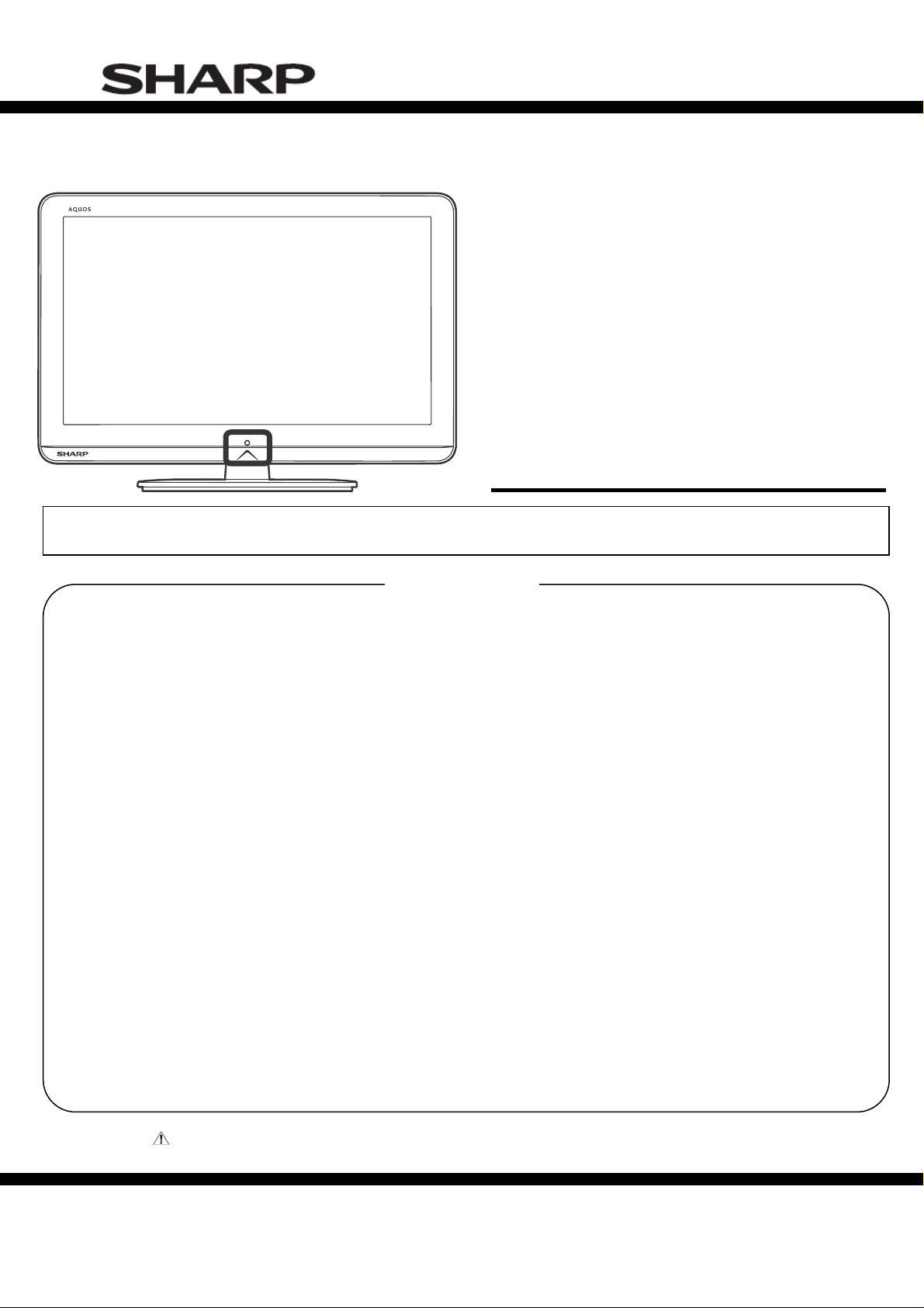
LC-19LE320
LC-22LE320
LC-26LE320
LC-32LE320
LC-37LE320
MODELS LC-42LE320
In the interests of user-safety (Required by safety regulations in some countries) the set should be restored to its origin
SAFETY PRECAUTION
IMPORTANT SERVICE SAFETY PRE-
CAUTION ................................................. ... .................2
Precautions for using lead-free solder ......……….........3
CHAPTER 1. OPERATION MANUAL
[1] SPECIFICATIONS ..................................................4
[2] OPERATION MANUAL ...........................................6
[3] DIMENSIONS ........................................................11
CHAPTER 2. REMOVING OF MAJOR PARTS
[1] REMOVING OF MAJOR PARTS ..........................12
CHAPTER 3. ADJUSTMENT PROCEDURE
[1] ADJUSTMENT PROCEDURE...............................22
[2] SERVICE MODE....................................................35
[3]
SOFTWARE UPGRADE PROCEDURE................36
CHAPTER 4. TROUBLESHOOTING TABLE
[1] TROUBLESHOOTING TABLE...............................37
CHAPTER 5. MAJOR IC INFORMATIONS
[1] MAJOR IC INFORMATIONS..................................75
CHAPTER 6. BLOCK DIAGRAM/WIRING DIAGRAM
[1] BLOCK DIAGRAM..................................................97
Parts marked with " " are important for maintaining the safety of the set. Be sure to replace these parts with specified ones for maintaining the
safety and performance of the set.
SHARP CORPORATION
ified should be
CONTENTS
[2] POWER MANAGEMENT BLOCK DIAGRAM ..........99
[3] WIRING DIAGRAM ................................................101
CHAPTER 7. PRINTED WIRING BOARD
[1] MAIN UNIT PRINTED WIRING BOARD .................103
[2] POWER UNIT PRINTED WIRING BOARD.............107
[3] KEY UNIT PRINTED WIRING BOARD ...................115
[4] IR UNIT PRINTED WIRING BOARD ......................116
[5] MEMC SCHEMATIC DIAGRAM..............................117
[6] RS232 SCHEMATIC DIAGRAM..............................119
[7] Convert SCHEMATIC DIAGRAM............................120
CHAPTER 8. SCHEMATIC DIAGRAM
[1] MAIN SCHEMATIC DIAGRAM ..............................122
[2] POWER SCHEMATIC DIAGRAM............................148
[3] KEY SCHEMATIC DIAGRAM..................................153
[4] IR SCHEMATIC DIAGRAM......................................154
[5] MEMC SCHEMATIC DIAGRAM..............................155
[6] RS232 SCHEMATIC DIAGRAM..............................160
[7] Convert SCHEMATIC DIAGRAM............................161
CHAPTER 9. Parts Guide
[1] SPARE PARTS LIST...............................................163
[2] CABINET PARTS ...................................................178
[3] SUPPLIED ACCESSOORIES............................... ..184
[4] PACKING PARTS....................................................185
1
.
This document has been published to be used for
after sales service only.
The contents are subject to change without notice.
Page 2
LC-19LE320, LC-22LE320, LC-26LE320, LC-32LE320, LC-37LE320, LC-42LE320
SAFETY PRECAUTION
IMPORTANT SERVICE SAFETY PRECAUTION
■ Service work should be performed only by qualified service technicians who are thoroughly familiar with all safety checks and the
servicing guidelines which follow:
■ WARNING
1. For continued safety, no modification of any circuit should be
attempted.
2. Disconnect AC power before servicing.
CAUTION:
FOR CONTINUED PROTECTION AGAINST A
RISK OF FIRE REPLACE ONLY WITH SAME
TYPE FUSE.
42" F901 (T6.3AH/250V)
26"/32" F901 (T5AH/250V)
■
BEFORE RETURNING THE RECEIVER
(Fire & Shock Hazard)
Before returning the receiver to the user, perform the following
safety checks:
3. Inspect all lead dress to make certain that leads are not pinched,
and check that hardware is not lodged between the chassis and
other metal parts in the receiver.
4. Inspect all protective devices such as non-metallic control knobs,
insulation materials, cabinet backs, adjustment and compartment
covers or shields, isolation resistor-capacitor networks, mechanical
insulators, etc.
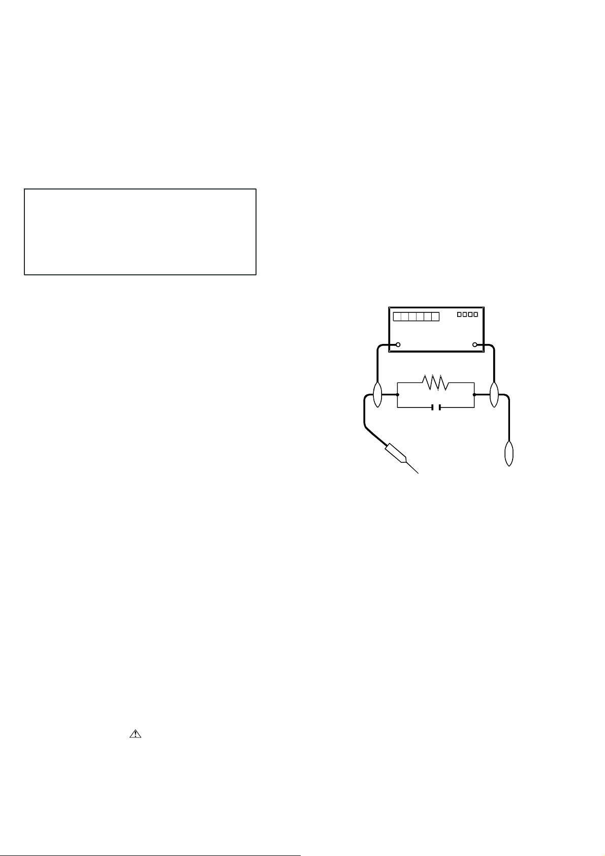
5. To be sure that no shock hazard exists, check for leakage current in
the following manner.
• Plug the AC cord directly into a 220~240 volt AC outlet.
• Using two clip leads, connect a 1.5k ohm, 10 watt resistor paralleled
by a 0.15µF capacitor in series with all exposed metal cabinet
parts and a known earth ground, such as electrical conduit or
electrical ground connected to an earth ground.
//////////////////////////////////////////////////////////////////////////////////////////////////////////////////////////////////////////////////////////////////////////////////////////////////////////////////////////////////////////////////
SAFETY NOTICE
Many electrical and mechanical parts in LCD color television have
special safety-related characteristics.
These characteristics are often not evident from visual inspection,
nor
can protection afforded by them be necessarily increased by using
replacement components rated for higher voltage, wattage, etc.
Replacement parts which have these special safety characteristics
are identified in this manual; electrical components having such
features are identified by “ ” and shaded areas in the Replacement
Parts List and Schematic Diagrams.
//////////////////////////////////////////////////////////////////////////////////////////////////////////////////////////////////////////////////////////////////////////////////////////////////////////////////////////////////////////////////
• Use an AC voltmeter having with 5000 ohm per volt, or higher, sen-
sitivity or measure the AC voltage drop across the resistor.
• Connect the resistor connection to all exposed metal parts having a
return to the chassis (antenna, metal cabinet, screw heads, knobs
and control shafts, escutcheon, etc.) and measure the AC voltage
drop across the resistor.
All checks must be repeated with the AC cord plug connection
reversed. (If necessary, a nonpolarized adaptor plug must be used
only for the purpose of completing these checks.)
Any reading of 1.05 V peak (this corresponds to 0.7 mA peak AC.)
or more is excessive and indicates a potential shock hazard which
must be corrected before returning the monitor to the owner.
DVM
AC SCALE
1.5k ohm
10W
0.15 µF
TEST PROBE
TO EXPOSED
METAL PARTS
CONNECT TO KNOWN
EARTH GROUND
For continued protection, replacement parts must be identical to those
used in the original circuit.
The use of a substitute replacement parts which do not have the same
safety characteristics as the factory recommended replacement parts
shown in this service manual, may create shock, fire or other hazards.
2
Page 3

LC-19LE320, LC-22LE320, LC-26LE320, LC-32LE320, LC-37LE320, LC-42LE320
Precautions for using lead-free solder
Using lead-free wire solder
• When fixing the PWB soldered with the lead-free solder, apply lead-free wire solder. Repairing with conventional lead wire solder may cause
damage or accident due to cracks.
As the melting point of lead-free solder (Sn-Ag-Cu) is higher than the lead wire solder by 40 °C, we recommend you to use a dedicated soldering
bit, if you are not familiar with how to obtain lead-free wire solder or soldering bit, contact our service station or service branch in your area.
Soldering
• As the melting point of lead-free solder (Sn-Ag-Cu) is about 220 °C which is higher than the conventional lead solder by 40 °C, and as it has
poor solder wettability, you may be apt to keep the soldering bit in contact with the PWB for extended period of time. However, Since the land
may be peeled off or the maximum heat-resistance temperature of parts may be exceeded, remove the bit from the PWB as soon as you
confirm the steady soldering condition.
Lead-free solder contains more tin, and the end of the soldering bit may be easily corroded. Make sure to turn on and off the power of the bit as
required.
If a different type of solder stays on the tip of the soldering bit, it is alloyed with lead-free solder. Clean the bit after every use of it.
When the tip of the soldering bit is blackened during use, file it with steel wool or fine sandpaper.
• Be careful when replacing parts with polarity indication on the PWB silk.
3
Page 4
LC-19LE320, LC-22LE320, LC-26LE320, LC-32LE320, LC-37LE320, LC-42LE320
CHAPTER 1. OPERATION MANUAL
[1] SPECIFICATIONS
Specification
Item
LCD screen size
Number of dots
Video Colour System PAL/SECAM/NTSC 3.58/NTSC 4.43/PAL 60
TV-Standard
TV Function
Audio amplifier 3W × 2 3W × 2 5W × 2
Speaker TBD TBD TBD
Rear
Side
OSD language
Power Requirement AC 220–240 V, 50 Hz
Power Consumption TBD
Weight
Operating temperature 0°C to + 40°C
• As a part of policy of continuous improvement, SHARP reserves the right to make design and specification changes for product improvement
without prior notice. The performance specification figures indicated are nominal values of production units. There may be some deviations
from these values in individual units.
NOTE
• Refer to the inside back cover for dimensional drawings.
• Audio cannot be output through the HDMI terminal.
Receiving
Channel
TV-Tuning System Auto Preset 999 ch, Auto Label, Auto Sort
STEREO/BILINGUAL NICAM/A2
Antenna UHF/VHF 75
RS-232C D-sub 9 pin male connector
SCART SCART (AV input, Y/C input, RGB input, TV output )
PC IN D-sub 15 pin (AV input), Ø 3.5mm jack (Audio input)
Component Y/Pb(Cb)/Pr(Cr), RCA pin (L/R)
SPDIF OUT Digital audio output
AV OUT RCA pin (AV output)
HDMI 1 Digital video and audio input
C. I. (Common Interface) EN50221, R206001, CI Plus specification
AV IN RCA pin (AV input)
USB Software update, multi-media play
Headphones Ø 3.5mm jack (Audio output)
HDMI 2 Digital video and audio input
Analogue CCIR (B/G, I, D/K, L/L’)
Digital DVB-T (2K/8K OFDM), DVB-C
VHF/UHF ATV : IRA-E69, DVB-T : E5-E69
CATV S-band, S1–S41ch
19” LCD COLOUR TV,
Model: LC-19LE320E
19” diagonal 22” diagonal 26” diagonal
3,147,264 dots
(1366 × 768 × 3 dots)
English, German, French, Italian, Dutch, Spanish, Greek, Portuguese, Swedish, Finnish, Russian,
Polish, Turkish, Hungarian, Czech, Slovak, Danish, Norwegian, Estonian, Latvian, Lithuanian,
Slovenian, Bulgarian, Croatian, Romanian, Serbian, Ukrainian, Gaelic, Belarussian.
TBD (Without stand),
TBD (With stand)
22” LCD COLOUR TV,
Model: LC-22LE320E
6,220,800 dots
(1920 × 1080 × 3 dots)
30W (Standby < 0.3W)
(Method IEC62087)
TBD (Without stand),
TBD (With stand)
26” LCD COLOUR TV,
Model: LC-26LE320E
3,147,264 dots
(1366 × 768 × 3 dots)
TBD
TBD (Without stand),
TBD (With stand)
4
Page 5
LC-19LE320, LC-22LE320, LC-26LE320, LC-32LE320, LC-37LE320, LC-42LE320
Item
LCD screen size
Number of dots
Video Colour System PAL/SECAM/NTSC 3.58/NTSC 4.43/PAL 60
TV-Standard
TV Function
Audio amplifier 10W × 2 10W × 2 10W × 2
Speaker TBD TBD TBD
Rear
Side
OSD language
Power Requirement AC 220–240 V, 50 Hz
Power Consumption TBD TBD TBD
Weight
Operating temperature 0°C to + 40°C
• As a part of policy of continuous improvement, SHARP reserves the right to make design and specification changes for product improvement
without prior notice. The performance specification figures indicated are nominal values of production units. There may be some deviations
from these values in individual units.
NOTE
• Refer to the inside back cover for dimensional drawings.
• Audio cannot be output through the HDMI terminal.
Receiving
Channel
TV-Tuning System Auto Preset 999 ch, Auto Label, Auto Sort
STEREO/BILINGUAL NICAM/A2
Antenna UHF/VHF 75
SCART 1 SCART (AV input, Y/C input, RGB input, TV output )
SCART 2
PC IN D-sub 15 pin (AV input), Ø 3.5mm jack (Audio input)
Component Y/Pb(Cb)/Pr(Cr), RCA pin (L/R)
SPDIF OUT Digital audio output
AUDIO OUT RCA pin (L/R)
HDMI 1 Digital video and audio input
HDMI 2 Digital video and audio input
RS-232C D-sub 9 pin male connector
C. I. (Common Interface) EN50221, R206001, CI Plus specification
AV IN RCA pin (AV input)
USB Software update, multi-media play
Headphones Ø 3.5mm jack (Audio output)
HDMI 3 Digital video and audio input
Analogue CCIR (B/G, I, D/K, L/L’)
Digital DVB-T (2K/8K OFDM), DVB-C
VHF/UHF ATV : IRA-E69, DVB-T : E5-E69
CATV S-band, S1–S41ch
32” LCD COLOUR TV,
Model: LC-32LE320E
32” diagonal 37” diagonal 42” diagonal
6,220,800 dots
(1920 × 1080 × 3 dots)
SCART (AV input, Y/C input, monitor output [analogue source - ATV, SCART 1, SIDE AV;
digital source - DTV] )
English, German, French, Italian, Dutch, Spanish, Greek, Portuguese, Swedish, Finnish, Russian,
Polish, Turkish, Hungarian, Czech, Slovak, Danish, Norwegian, Estonian, Latvian, Lithuanian,
Slovenian, Bulgarian, Croatian, Romanian, Serbian, Ukrainian, Gaelic,Belarussian.
TBD (Without stand),
TBD (With stand)
37” LCD COLOUR TV,
Model: LC-37LE320E
6,220,800 dots
(1920 × 1080 × 3 dots)
TBD (Without stand),
TBD (With stand)
42” LCD COLOUR TV,
Model: LC-42LE320E
6,220,800 dots
(1920 × 1080 × 3 dots)
TBD (Without stand),
TBD (With stand)
2008-03-14
5
Page 6
LC-19LE320, LC-22LE320, LC-26LE320, LC-32LE320, LC-37LE320, LC-42LE320
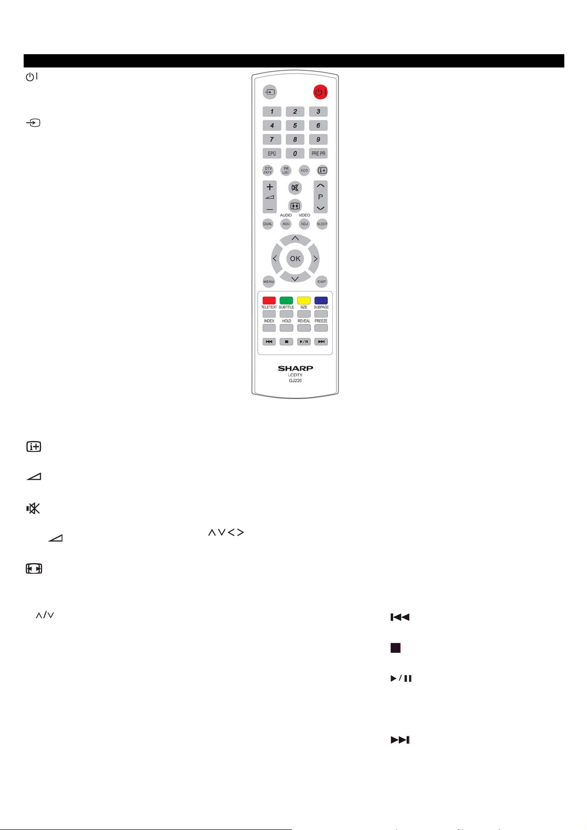
[2] OPERATION MANUAL
Remote control unit
(POWER)
Press to turn the LCD TV on or enter standby
mode.
(INPUT SOURCE)
Select an input source.
0-9 DIGIT BUTTONS
To select a TV channel directly.
EPG
Press this button to display electronic
programme guide when watching digital
channels.
PRE PR
To display the previous selected TV channel.
DTV/ATV
Press this button to switch between ATV and
DTV channels.
PR LIST
Press to display a list of channels. Then press
Red button to select the digital or analogue
channel list.(Only available when your input
source is TV).
ECO
Press this button to set the picture with less
brightness for saving energy.
Display programme information, if available.
(+/-)
Press to adjust the volume.
Press to toggle audio on and off. You can also
press
level.
Select picture format to Auto /Normal / Zoom
1/ Zoom 2 /Wide.
P (
Press to select the channel.
DUAL
Select MONO / STEREO / DUAL 1 / DUAL 2
for ATV channel. Select Audio language for
DTV channel.
AUDIO (ADJ)
Press to set the LCD TV to a predefined sound
setting.
Personal / Music / Speech
(+/-) to restore the previous volume
(Picture format)
)
VIDEO (ADJ)
Press to set the LCD TV to a predefined picture
setting.
Personal / Standard / Vivid /
Movie / Eco
SLEEP
Press to turn the LCD TV off within an amount
of time. (10 ~ 120 minutes.)
Press ooep to navigate and confirm your
selection.
OK
Press to activate a setting.
MENU
Press to activate the LCD TV OSD.
EXIT
Press to exit the LCD TV OSD or return to the
previous layer.
R/G/Y/B (COLOUR BUTTON)
Press buttons to select the pictures with various
colours of text. Different channels display
different functions.
TELETEXT
Press this button to activate Teletext. Press
again to activate Teletext with TV.
Press again to turn off Teletext.
SUBTITLE
For DTV, press this button to toggle off /
between available subtitle languages.
For ATV, press this button to toggle
off / between available subtitle pages
in Teletext.
SIZE
Press this button to change the font size: Full
screen, Top half and Bottom half.
SUBPAGE
To select the subpage when the current page
contains subpage(s).
INDEX
Press this button to return to page 100 or the
index page; and then press 0 to 9. The teletext
page will be numbered and added to the page
you select or the secondary item.
HOLD
Press this button to stop the scrolling of pages.
The text decoder stops receiving data.
REVEAL
Reveal hidden information such as answers to a
quiz.
FREEZE
Press to freeze a moving image on the screen.
(Only available when your input source is TV).
Scart output signal will also be frozen when you
are watching digital channels.
In USB mode:
(You need to programme the setting with
remote control to control connected devices.)
Press to skip back to the previous title or track.
Press to stop playback.
Press to start/pause playback. Caution: Do not
freeze the video image for long periods of time.
You may damage the TV screen.
Press to skip forward to the next title or track.
6
Page 7
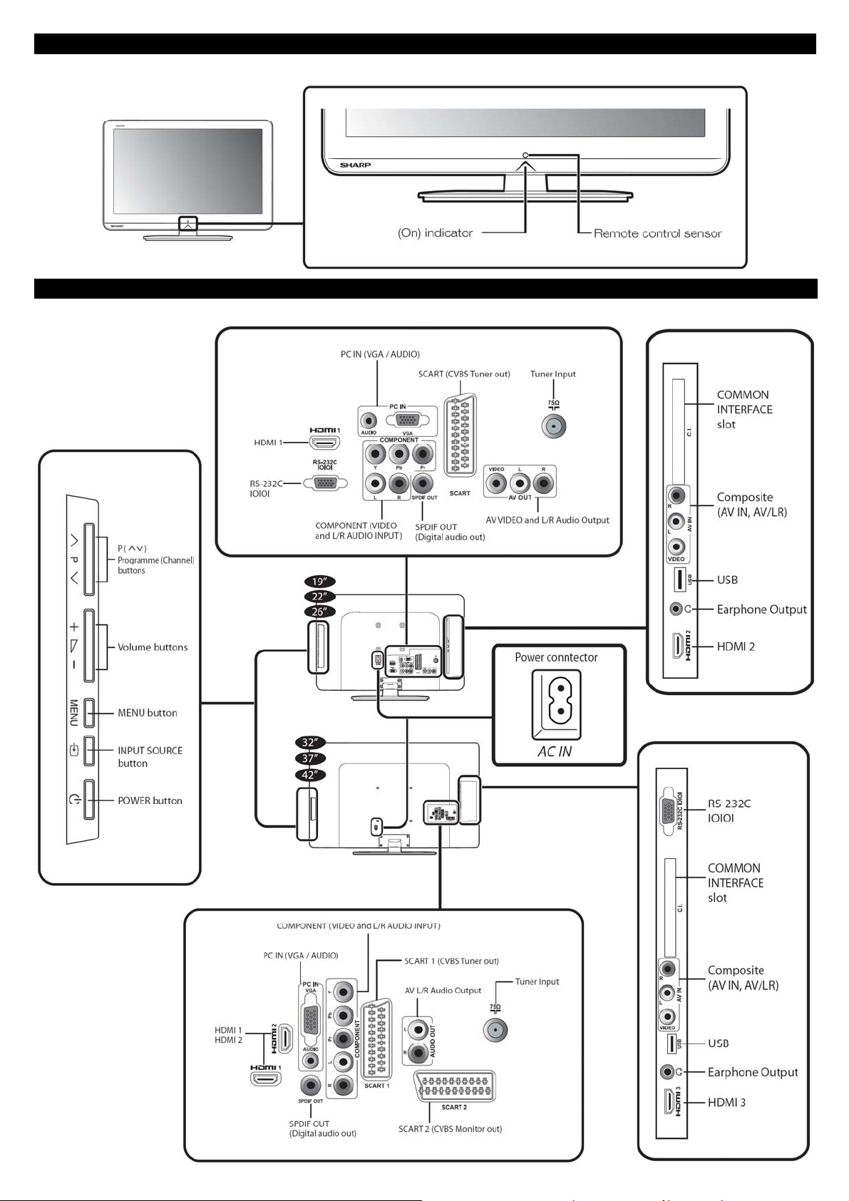
TV (Front view)
TV (Rear view)
LC-19LE320, LC-22LE320, LC-26LE320, LC-32LE320, LC-37LE320, LC-42LE320
2008-03-14
7
Page 8
LC-19LE320, LC-22LE320, LC-26LE320, LC-32LE320, LC-37LE320, LC-42LE320
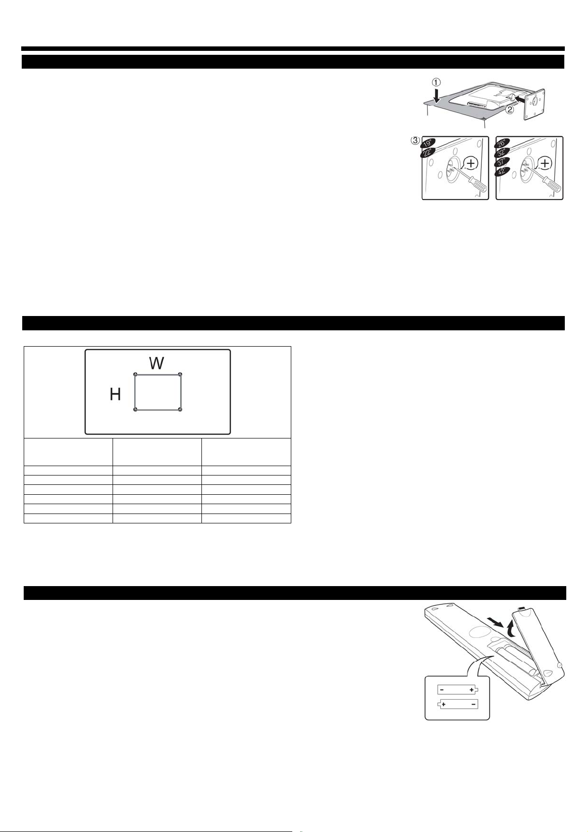
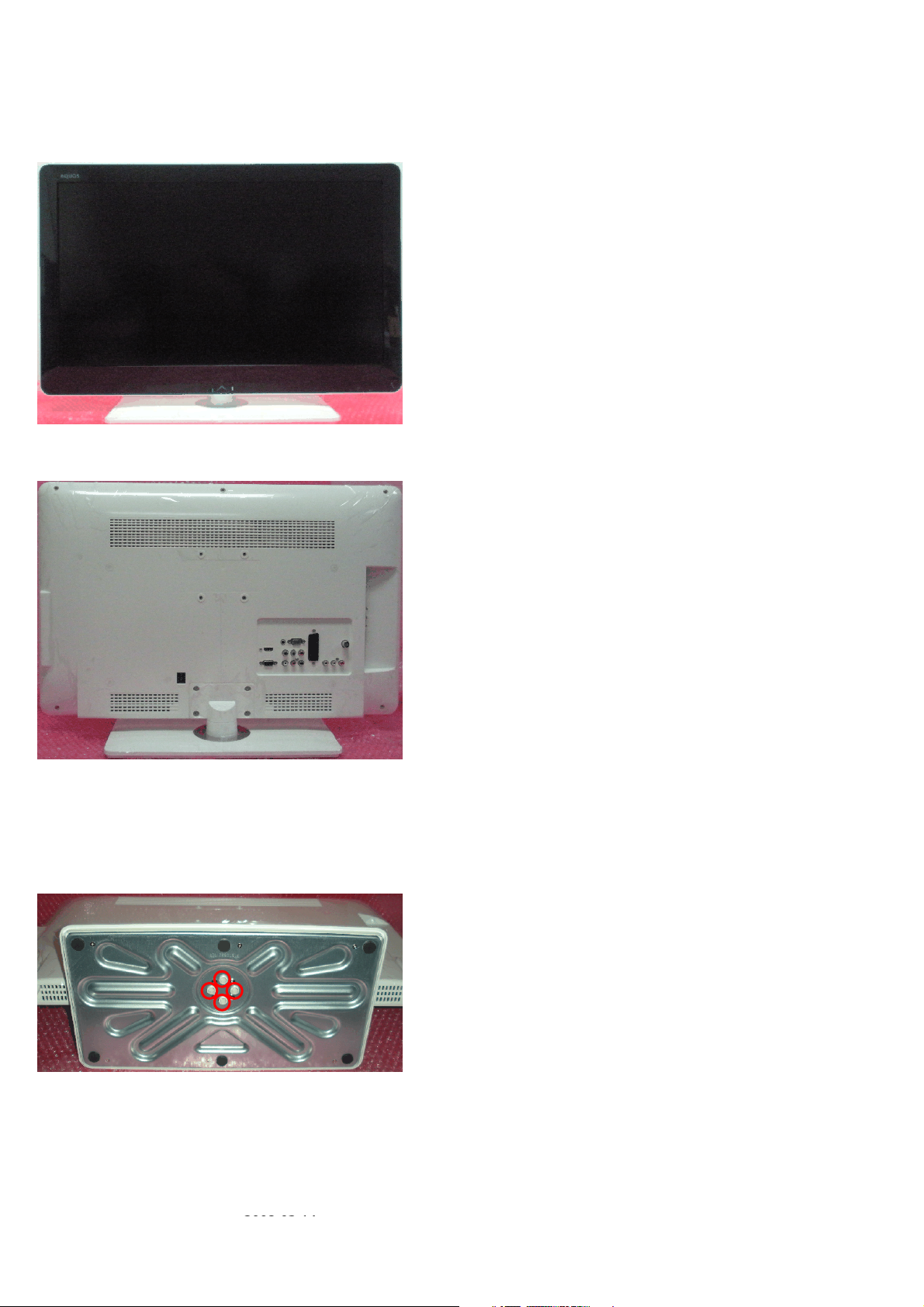
Preparation
Attaching/Detaching the Stand
• Before attaching (or detaching) the stand, unplug the AC cord from the AC INPUT terminal.
• Before performing work spread cushioning over the base area to lay the TV on. This will prevent it from
Being damaged.
CAUTION:
• Attach the stand in the correct direction.
• Be sure to follow the instructions. Incorrect installation of the stand may result in the TV falling over.
1. Put the TV face down on a safe surface
that is covered by a soft and smooth cloth.
2. Adjust the TV stand to the bottom of the TV.
3. Fasten the screws by using a cross-head screwdriver(Not supplied).
CAUTION:
• Do not push to hard or put excessive pressure to the stand neck to avoid the damages when you turn the TV for the most comfortable viewing
angle.
NOTE:
To detach the TV stand, perform the steps in reverse order.
Wall mounting
TV screen
size(Inches)
19” 75 x 75 mm Metric 4 x 10 mm
22” 75 x 75 mm Metric 4 x 10 mm
26” 75 x 75 mm Metric 4 x 10 mm
32” 200 x 100 mm Metric 6 x 10 mm
37” 200 x 200 mm Metric 6 x 10 mm
42” 200 x 200 mm Metric 6 x 10 mm
NOTE
• At the time of purchasing wall bracket, please check if there is enough space between the wall bracket and TV terminals for the terminal connection.
VESAcompatible wall
bracket(millimeters)
(W x H)
Screw type
Installing Batteries in the Remote Control Unit
1. Insert two AAA batteries into Remote control. Make sure (+) and (-) are facing the proper
direction.
2. Replace the cover
NOTE
• If the remote control will not to be used for a long time, remove the batteries to avoid remote control
damage.
CAUTION:
Improper use of batteries can result in chemical leakage or explosion. Be sure to follow the instructions below.
• Do not mix batteries of different types. Different types of batteries have different characteristics.
• Do not mix old and new batteries. Mixing old and new batteries can shorten the life of new batteries or cause chemical leakage in old batteries.
• Remove batteries as soon as they are worn out. Chemicals that leak from batteries come in contact with skin can cause a rash. If you find any chemical
leakage, wipe thoroughly with a cloth.
• The batteries supplied with this product may have a shorter life expectancy due to storage conditions.
8
Page 9
LC-19LE320, LC-22LE320, LC-26LE320, LC-32LE320, LC-37LE320, LC-42LE320
• If you will not be using the remote control unit for an extended period of time, remove batteries from it.
Note on disposing batteries:
The batteries provided contain no harmful materials such as cadmium, lead or mercury. Regulations concerning used batteries stipulate that batteries may
no longer be thrown out with the household rubbish. Deposit any used batteries free of charge into the designated collection containers set up at
commercial businesses.
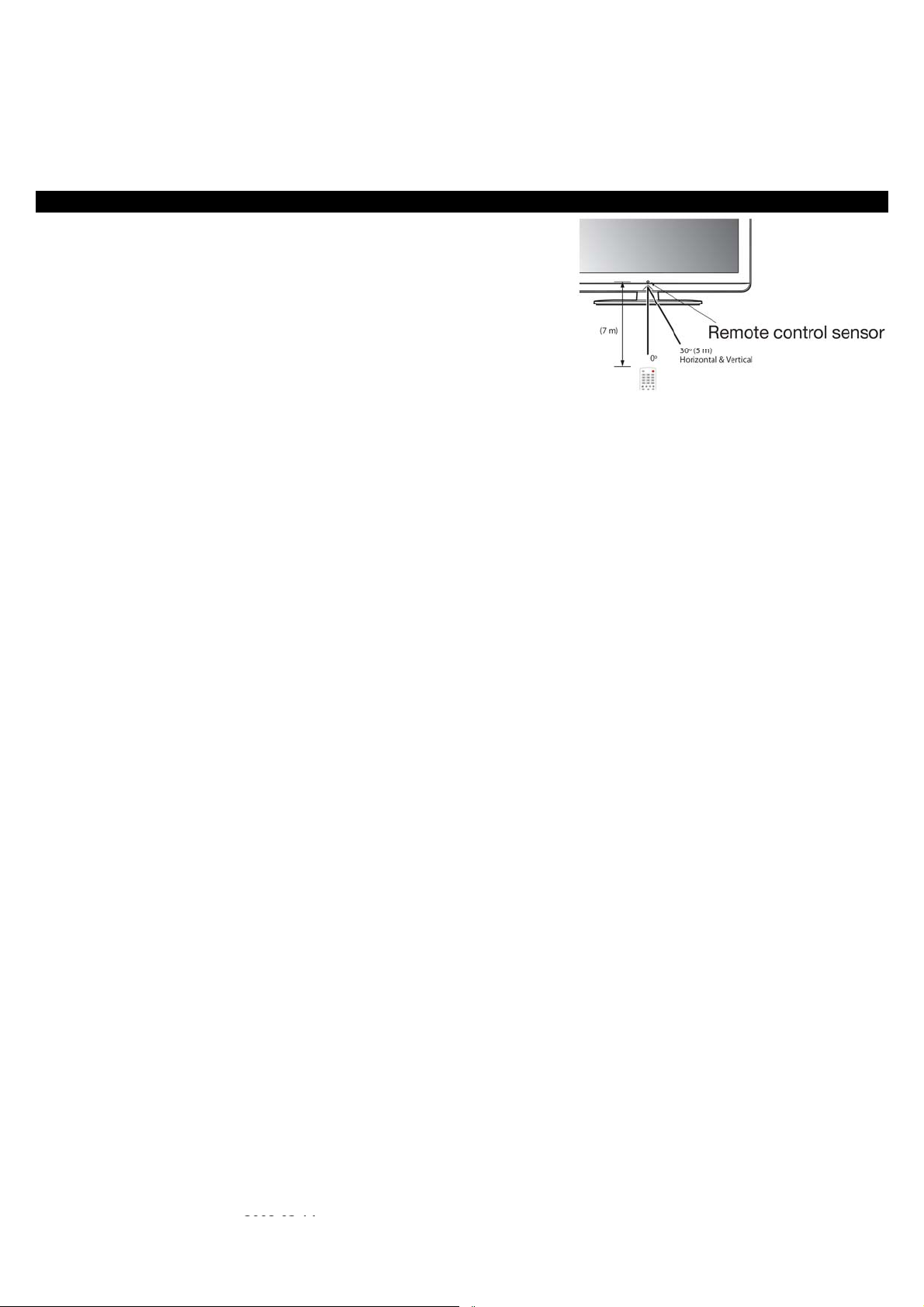
Installing Batteries in the Remote Control Unit
Use the remote control unit by pointing it towards the remote control sensor. Objects
between the remote control unit and sensor may prevent proper operation.
2008-03-14
9
Page 10
LC-19LE320, LC-22LE320, LC-26LE320, LC-32LE320, LC-37LE320, LC-42LE320
Appendix
troubleshooting
problem possible Solution
No picture 1. Connect power cord correctly.
Abnormal colours Connect signal cable correctly.
Twisted picture 1. Connect signal cable correctly.
Picture too dark Adjust brightness and contrast.
Audio only, no images 1. Please check if input signal is connected correctly.
Picture only, no audio 1. Connect signal cable correctly.
Cannot use remote control 1. Please change battery.
Cannot receive sufficient channels through
antenna
No colour Please adjust the colour setup.
Blinking picture accompanied by ghost image 1. Check the connection of antenna/signal cable.
Broken lines or segments Adjust antenna.
Certain TV channels are blocked(Hope to
acquire some channels)
Overlapping images or ghost images Please use multi-directional outdoor antenna.(If your TV is subject to the influence of nearby mountains or
Cannot use a function If the item you choose turns gray, that item cannot be selected.
Cannot receive programmes Please use the Update Scan method to add the channels not included in memory.
2. Turn on power.
3. Connect signal cable correctly.
4. Press any button on the LCD TV.
2. Please use compatible signal.
2. TV-RF signal must not be lower than 50dB.
2. Adjust volume to proper level.
3. Connect audio signal cable correctly.
4. TV-RF signal must not be lower than 50dB.
2. Turn off power for 10 seconds; and then restart power.
Please use the Channel Scan function to increase the number of channels not included in memory.
2. Check if channel is in play mode.
3. Press signal source and change input mode.
Keep the TV away from noise sources, such as automobiles, neon lights, and hair dryers.
Please use the Update Scan method to add the channels not included in memory.
buildings).
10
Page 11
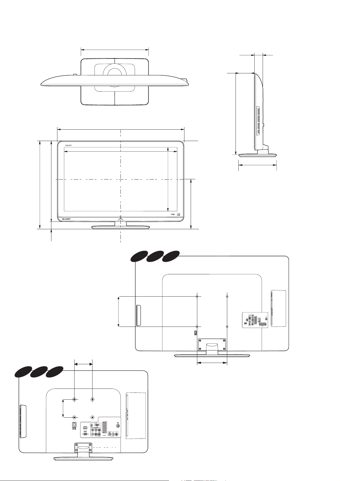
[3] DIMENSIONS
Dimension
/
]
71.054
[
/
))
0.273
{
/}}5.866{{ / }5.806
((
]]
/
3.535
)
0.533
[[
(
(
246.0)/((246.0))/[389.97]/[[418.0]]/ {460.0} / {{500.0}}
(
468.4)/((536.0))/[647.35]/[[786.6]]/ {907.5} / {{1018.5}}
/
]
72.514
[
/
))
0.243
/}}5.036{{ / }0.865{
((
]]
/
3.005
)
0.403
[[
(
/
/
]]
}}0.83{
00.53
))
0.03
[[
((
{/ }0.83{
/
/
)
]
0
1.01
.13
(
[
LC-19LE320, LC-22LE320, LC-26LE320, LC-32LE320, LC-37LE320, LC-42LE320
(
411.205)/((477.64))/[577.25]/
[[
700.67]]/ {821.5} / {{932.5}}
}}
0.0
0
2{{
/
}
0.00
2
{
/
]
]0.
0
01
[
[
(
38.6)/((38.6))/[39.6]/
[[
44.9]]/ {44.9} / {{44.9}}
(
70.3)/((70.3))/[87.49]/
[[
95.7]]/ {106.0} / {{118.5}}
/
]
}}5
71.523
.
525{{ / }
[
/
))
0.3
11.962
6
4
{
/
((
]]
/
)
7
508.132
3.5
93
[
[
(
”73
”
23
”24
/
5
]
7.263{{ / }5.13
45.252
[
/
))
0.012
3
{
/}}
(
(
]]
/
5
)
6
0.291
.4
9
2
(
[[
(
170.0)/((170.0))/[215.98]/
[[
238.0]]/ {250.0} / {{260.0}}
(
) / ((75.0)) / [75.0]
75.0
[[
”91
”22
”62
200.0]]/{200.0}/ {{200.0}}
( ): 19"
(( )): 22"
(
(
/
)]0.57[ / ))0.57
0.57
(
2008-03-14
[ ]: 26"
[[ ]]: 32"
{ } : 37"
{{ }} : 42"
11
Page 12
LC-19LE320, LC-22LE320, LC-26LE320, LC-32LE320, LC-37LE320, LC-42LE320
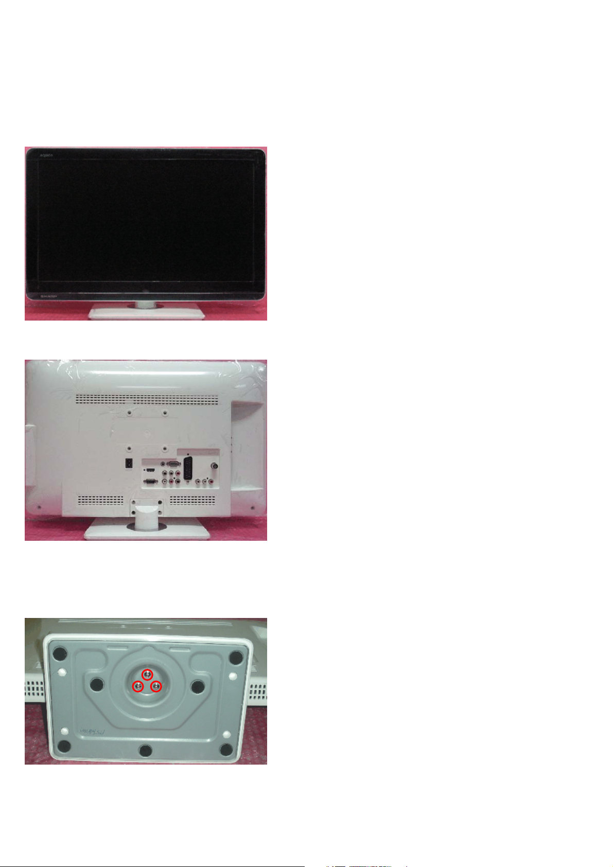
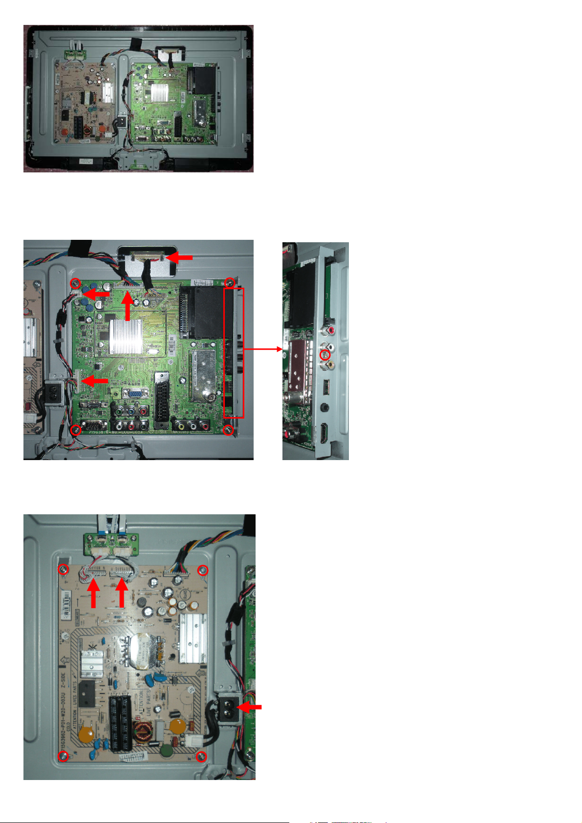
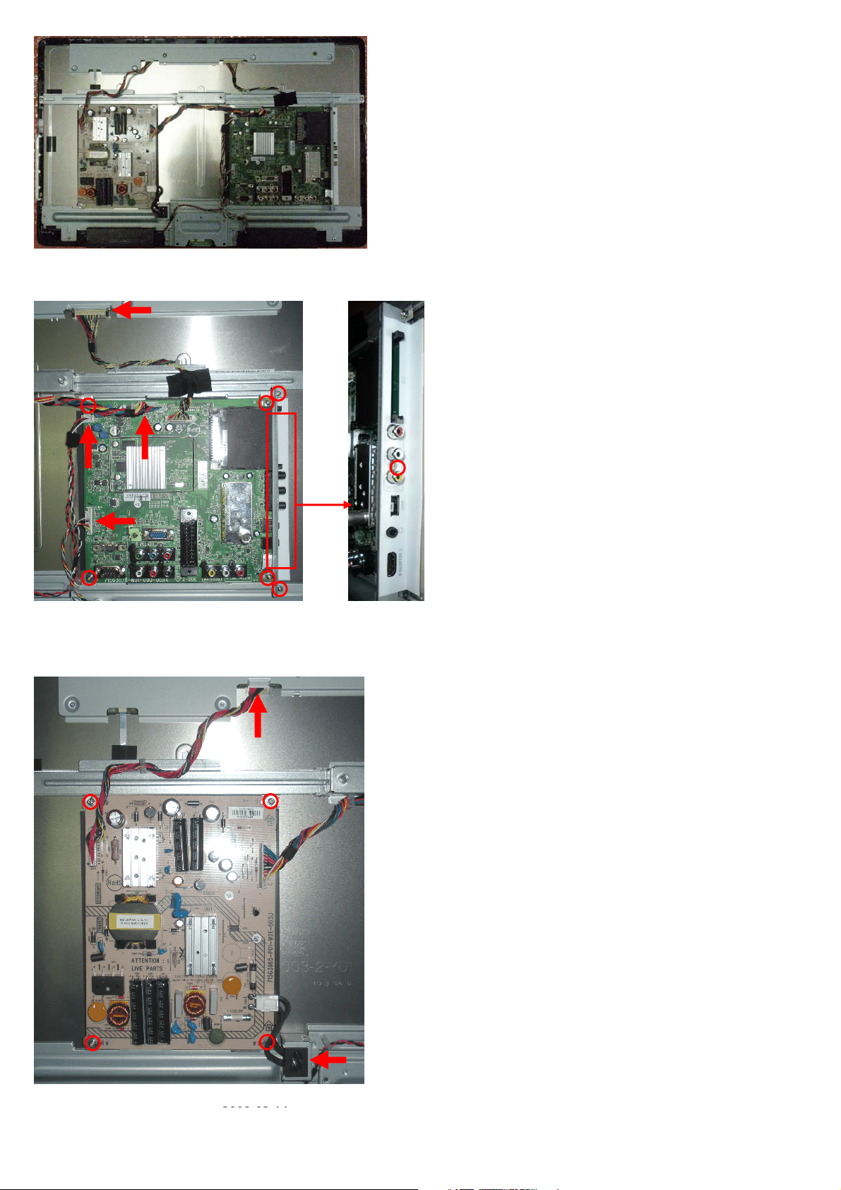
CHAPTER 2. REMOVING OF MAJOR PARTS
[1] REMOVING OF MAJOR PARTS(LC-22LE320)
1. Assy/Panel Removal
Notes: Please put your machine on soft material to avoid to scrape panel when you disassemble it.
Front view
Fig.1
Back view
Fig.2
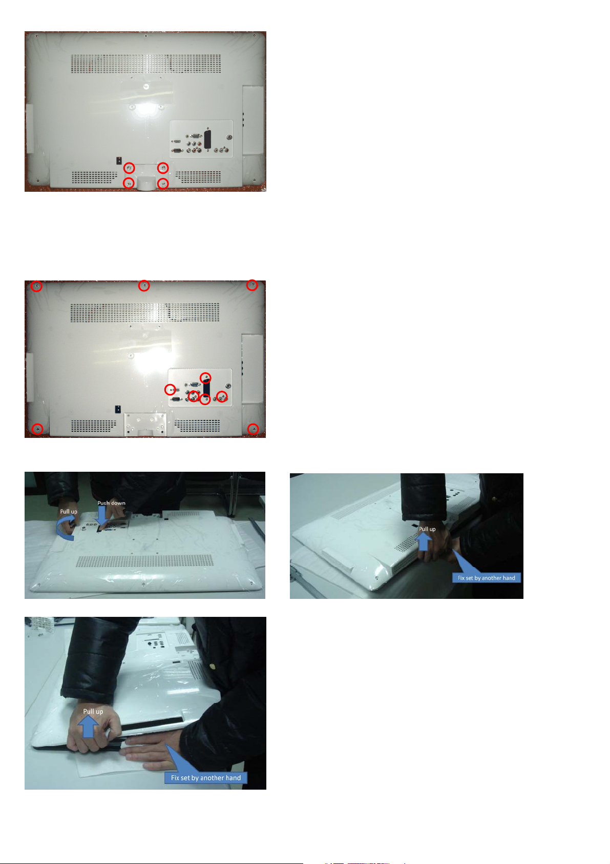
Step 1. Remove the Base Assy and Base neck.
1. Remove the Base Assy as Fig.3.
Remove the 3 screws as Fig.3 and pull out the base as Fig.4
Fig.3
12
Page 13
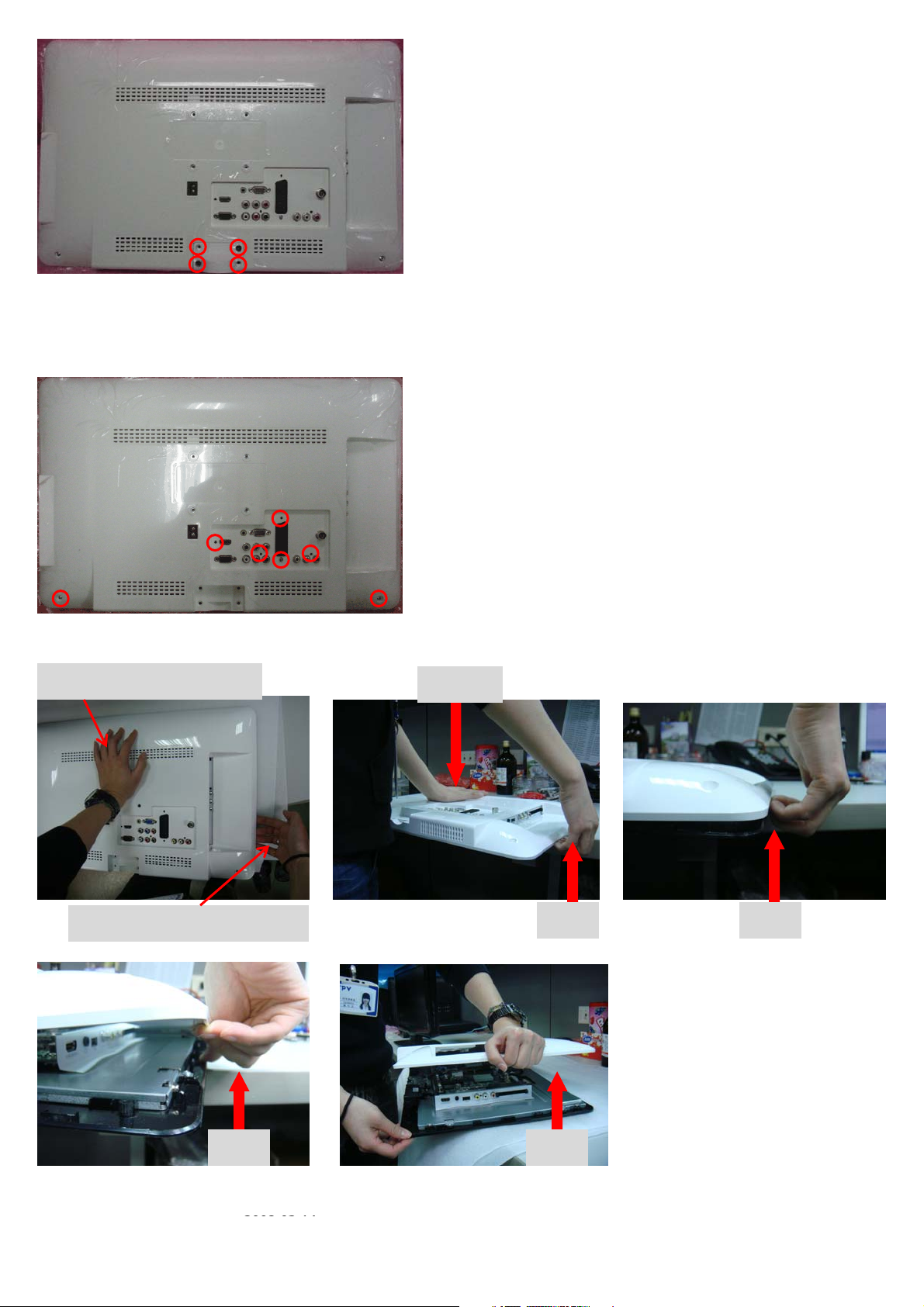
LC-19LE320, LC-22LE320, LC-26LE320, LC-32LE320, LC-37LE320, LC-42LE320
Fig.4
2. Remove the 4 screws. Detach the Base neck as Fig.4.
Step 2. Remove the REAR COVER Assy.
1. Remove the 7 screws. Detach the REAR COVER as Fig.5.
Fig.5
Note: How to easy remove rear cabinet
Put left hand on the center of rear cabinet
Right hand fingers put under the machine rim
Press down
Pull up Pull up
Pull up Pull up
Step 3. Remove the Main, Power, Convert board and the Speakers.
2008-03-14
13
Page 14
LC-19LE320, LC-22LE320, LC-26LE320, LC-32LE320, LC-37LE320, LC-42LE320
Fig.6
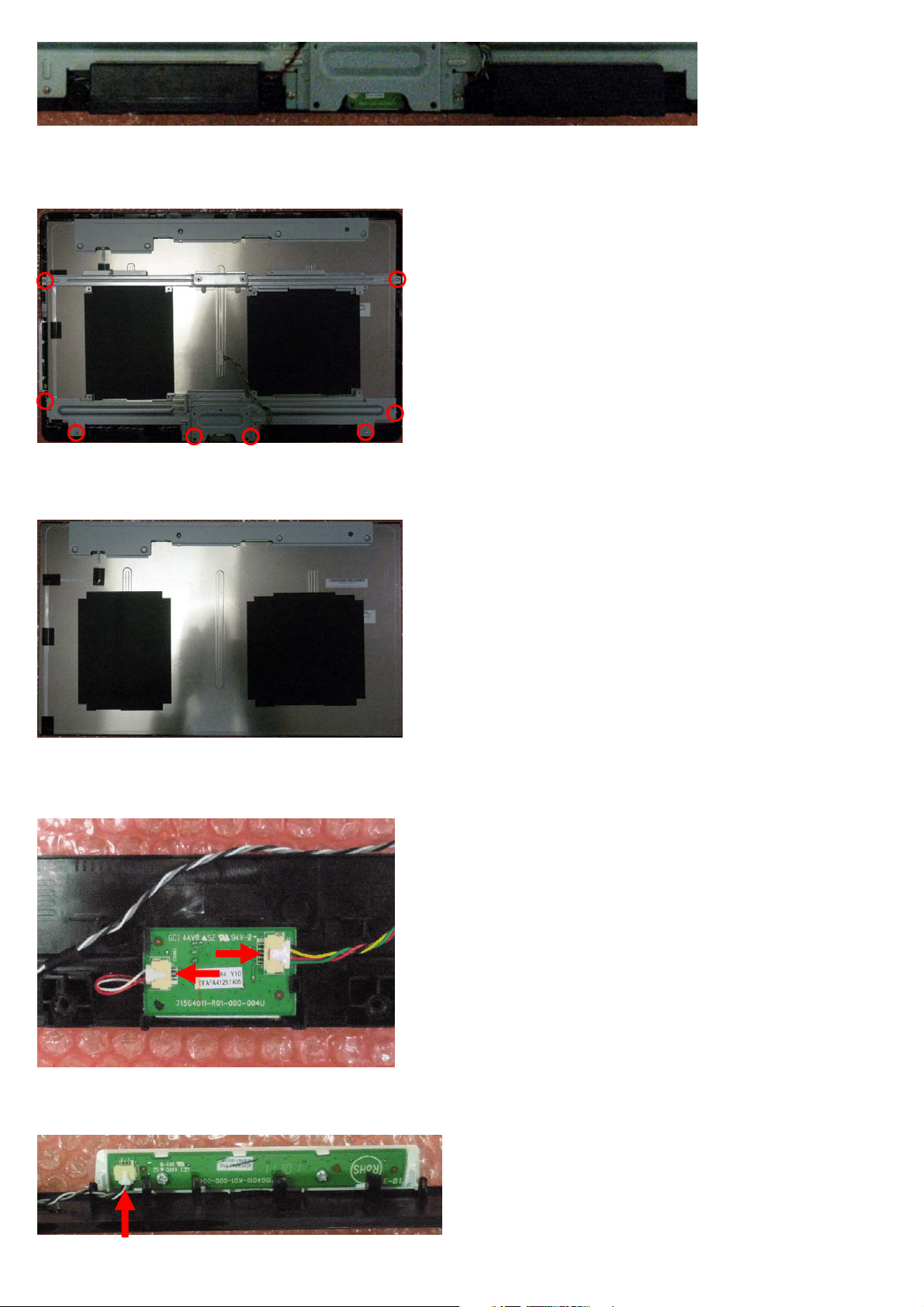
1. Remove the 5 screws and disconnect 4 cables. Detach the Main board as Fig.7 and Fig.8.
Note: Please disconnect the LVDS cable with the panel firstly, then disconnect the LVDS with the main board.
If you disconnect the LVDS cable with the Main board firstly, maybe the panel connector will be damaged because of the short LVDS cable.
Fig.7 Fig.8
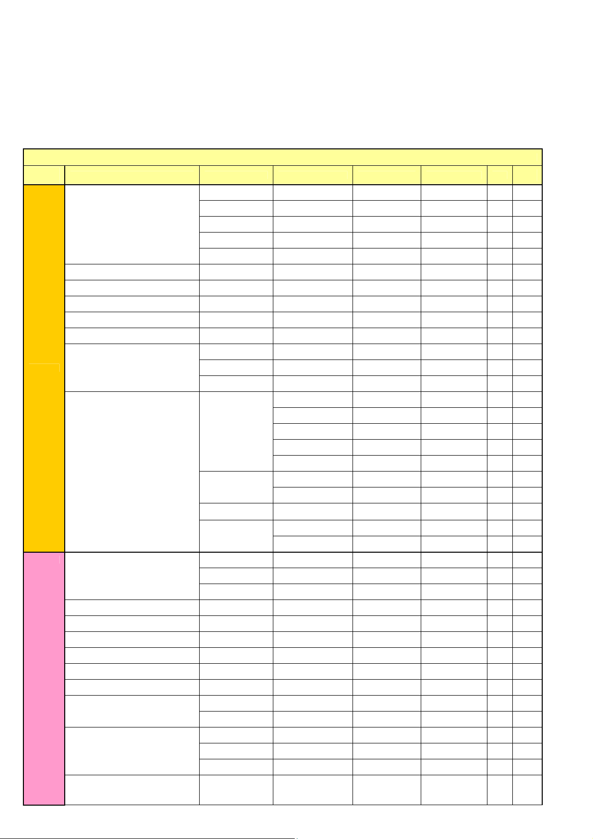
2. Remove the 4 screws and disconnect 3 cables. Detach the Power board as Fig.9.
Note: Move the AC port left from the Main frame assy, then disconnect the AC cable from the power board.
Fig.9
14
Page 15
LC-19LE320, LC-22LE320, LC-26LE320, LC-32LE320, LC-37LE320, LC-42LE320
3. Remove the 2 screws and disconnect 2 cables. Detach the Convert board as Fig.10.
Fig.10
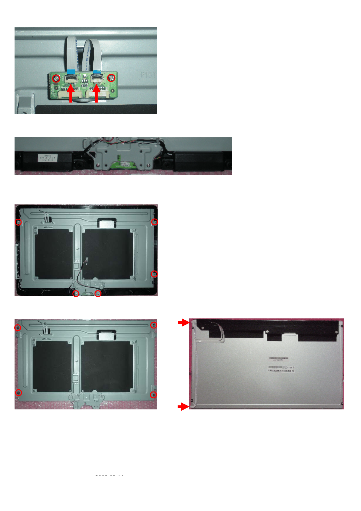
4. Release the speaker cable from its clamp, pull up and remove the speaker as Fig.11.
Fig.11
Step 4. Remove the Bracket and Bezel.
1. Remove the 5 screws. Detach the Bracket and panel as Fig.12.
Fig.12
2. Remove the 4 screws. Detach the Main frame as Fig.13. Disconnect the two FFC cables from the panel as Fig.14
Fig.13 Fig.14
Panel:
2008-03-14
15
Page 16

LC-19LE320, LC-22LE320, LC-26LE320, LC-32LE320, LC-37LE320, LC-42LE320
Fig.15
Step 5. Remove the IR and Key board.
1. Remove the 2 screws and disconnect 2 cables. Detach the IR board as Fig.16.
Fig.16
2. Disconnect 1 cable. Detach the Key board as Fig.17.
Fig.17
2. Set Re-assembly
To re-assemble the whole set, execute all processes in reverse order.
Notes:
a. While re-assembling, make sure that all cables are placed and connected in their original position.
b. Pay special attention not to damage the EMC foams at the SSB shielding. Check that EMC foams are put
correctly on their places.
16
Page 17
LC-19LE320, LC-22LE320, LC-26LE320, LC-32LE320, LC-37LE320, LC-42LE320
REMOVING OF MAJOR PARTS(LC-26LE320)
1. Assy/Panel Removal
Notes: Please put your machine on soft material to avoid to scrape panel when you disassemble it.
Front view
Fig.1
Back view
Fig.2
Step 1. Remove the Base Assy and Base neck.
1. Remove the Base Assy as Fig.3.
Remove the 4 screws as Fig.3 and pull out the base as Fig.4
Fig.3
2008-03-14
17
Page 18
LC-19LE320, LC-22LE320, LC-26LE320, LC-32LE320, LC-37LE320, LC-42LE320
Fig.4
2. Remove the 4 screws. Detach the Base neck as Fig.4.
Step 2. Remove the REAR COVER Assy.
1. Remove the 10 screws. Detach the REAR COVER as Fig.5.
Fig.5
Note: How to easy remove rear cabinet
Step 3. Remove the Main, Power board and the Speakers.
18
Page 19
LC-19LE320, LC-22LE320, LC-26LE320, LC-32LE320, LC-37LE320, LC-42LE320
Fig.6
1. Remove the 7 screws and disconnect 4 cables. Detach the Main board as Fig.7 and Fig.8.
Fig.7 Fig.8
2. Remove the 4 screws and disconnect 2 cables. Detach the Power board as Fig.9.
Note: Move the AC port left from the Main frame assy, then disconnect the AC cable from the power board.
Fig.9
4. Release the speaker cable from its clamp, pull up and remove the speaker as Fig.10.
2008-03-14
19
Page 20
LC-19LE320, LC-22LE320, LC-26LE320, LC-32LE320, LC-37LE320, LC-42LE320
Fig.10
Step 4. Remove the Bracket and Bezel.
1. Remove the 6 screws. Detach the Bracket as Fig.11.
Fig.11
2. Remove the panel from the bezel as Fig.12
Panel:
Fig.12
Step 5. Remove the IR and Key board.
1. Disconnect 2 cables, then release the clips. Detach the IR board as Fig.13.
Fig.13
2. Disconnect 1 cable. Detach the Key board as Fig.17.
Fig.17
20
Page 21

LC-19LE320, LC-22LE320, LC-26LE320, LC-32LE320, LC-37LE320, LC-42LE320
2. Set Re-assembly
To re-assemble the whole set, execute all processes in reverse order.
Notes:
a. While re-assembling, make sure that all cables are placed and connected in their original position.
b. Pay special attention not to damage the EMC foams at the SSB shielding. Check that EMC foams are put
correctly on their places.
2008-03-14
21
Page 22
LC-19LE320, LC-22LE320, LC-26LE320, LC-32LE320, LC-37LE320, LC-42LE320
CHAPTER 3. ADJUSTMENT PROCEDURE
PROCEDURE
[1] ADJUSTMENT PROCEDURE
1. OSD Menu
2K10 Sharp DVB OSD tree-Video
OSD
Layer 1
Picture
Sound
2 3 4 5 6 Note
Personal
Standard
Smart Picture
Brightness slider All
Contrast slider All
Color slider All
Tint slider All
Sharpness slider All
Color Temperature
Advanced Control(have sub page)
Sound Mode
Equilizer 120Hz slider All
Equilizer 500Hz slider All
Equilizer 1.5KHz slider All
Equilizer 5KHz slider All
Equilizer 10KHz slider All
Balance slider All
Virtual Surround
Digital Audio Out
SPDIF Delay
Vivid
Movie
Eco
Normal (default) All
Cool All
Warm All
Noise Reduction
Flesh Tone
Back Light(if DCR is
Off)
DCR
Personal
Music
Speech
On All
Off All
PCM All
Off All
Dolby Digital All
slider(from 0 to 250,
interval of 10
between two items)
Model
All
All
All
All
All
Off All
Low All
Medium All
HIGH All
Auto All
On All
Off All
slider All
On All
Off All
All
All
All
All
22
Page 23
AVL
Type(if source is DTV)
LC-19LE320, LC-22LE320, LC-26LE320, LC-32LE320, LC-37LE320, LC-42LE320
Off All
On All
Normal All
Hard of Hearing All
Audio Description All
TV
Audio Description(if Type=Audio
Description)
Tuner Mode
Country(30)
1st Audio(28)(DTV only)
2008-03-14
Volume slider
Antenna
Cable
UK
Italy
Luxembourg
Netherlands
Norway
Sweden
Croatia
Hungary
Ireland
Poland
Portugal
Romania
Serbia
Slovakia
Slovenia
Turkey
Iceland
Russia
Ukraine
Austria
Belgium
Bulgaria
Switzerland
Czech Republic
Germany
Greece
Denmark
Spain
Finland
France
English
Finnish
French
Gaelic
Galician
German
Greek
All
All
All
All
All
All
All
All
All
All
All
All
All
All
All
All
All
All
All
All
All
All
All
All
All
All
All
All
All
All
All
All
All
All
All
All
All
All
All
All
All
All
23
Page 24
LC-19LE320, LC-22LE320, LC-26LE320, LC-32LE320, LC-37LE320, LC-42LE320
2nd Audio(28)(DTV only)
Hungarian
Italian
Norwegian
Polish
Portuguese
Romanian
Russian
Serbian
Slovak
Slovenian
Spanish
Swedish
Turkish
Welsh
Basque
Bulgarian
Catalan
Croatian
Czech
Danish
Dutch
English
Finnish
French
Gaelic
Galician
German
Greek
Hungarian
Italian
Norwegian
Polish
Portuguese
Romanian
Russian
Serbian
Slovak
Slovenian
Spanish
Swedish
Turkish
Welsh
Basque
Bulgarian
Catalan
Croatian
Czech
Danish
Dutch
All
All
All
All
All
All
All
All
All
All
All
All
All
All
All
All
All
All
All
All
All
All
All
All
All
All
All
All
All
All
All
All
All
All
All
All
All
All
All
All
All
All
All
All
All
All
All
All
All
24
Page 25
Audio Carrier(ATV only)
Channels(have sub page)
Features Menu Language(28)
2008-03-14
LC-19LE320, LC-22LE320, LC-26LE320, LC-32LE320, LC-37LE320, LC-42LE320
Mono
Stereo
Dual I
Dual II
Channel Scan
Update Scan
Single RF Scan
Analog Manual
Scan
Channel Skip(have
sub page)
Channel Sort(have
sub page)
Channel Edit(have
sub page)
Decoder(for ATV) (Channel munber…) All
Analog Ch Fine
Tune
English
Deutsch
Français
Italiano
Español
Português
Nederlands
Dansk
Suomi
Svenska
Norsk
Polski
esky
All
All
All
All
ATV
ATV and DTV( if
Antenna mode)
Digital channels: All
ATV and DTV( if
Cable mode)
Frequency(KHz) All
Scan
Digital channels: All
Status: scanning… All
Analogue channels: All
Digital channels: All
RF Channel .. slider All
Signal Strength.. All
Signal Quailty.. All
Start Frequency xxMHz All
Scan Up All
Scan Down All
(Channel munber…) All
(Channel munber…) All
(Channel munber…) All
(Channel munber…)
(have sub page)
All
All
All
All
All
All
All
All
All
All
All
All
All
All
All
Status:
scanning…
Analogue
channels:
Status:
scanning…
Analogue
channels:
Scan Mode Full/Advance All
(if Advance mode
select)
(do fine tune) All
All
All
All
All
Modulation
=>Auto/16/32/64/
128/256 QAM
Symbol
Rate(Ksym/s)
Network ID All
Status:
scanning…
Analogue
channels:
All
All
All
All
25
Page 26
LC-19LE320, LC-22LE320, LC-26LE320, LC-32LE320, LC-37LE320, LC-42LE320
Hrvatski
Magyar
Român
Slovenský
Slovenšina
Srpski
Türkçe
Gaeilge
Latviski
Eesti
Lietuviskai
ykpaiHcbka
4:3 mode
Picture Format(if video exist)
Time (have sub page ) Time Zone
4:3
16:9
Auto
Normal
Zoom1
Zoom2
Wide
All
All
All
All
All
All
All
All
All
All
All
All
All
All
All
All
All
All
All
All
As Broadcaster All
GMT +0:00 All
GMT +1:00 All
GMT +2:00 All
GMT +3:00 All
GMT +3:30 All
GMT +4:00 All
GMT +4:30 All
GMT +5:00 All
GMT +5:30 All
GMT +5:45 All
GMT +6:00 All
GMT +6:30 All
GMT +7:00 All
GMT +8:00 All
GMT +9:00 All
GMT +9:30 All
GMT +10:00 All
GMT +11:00 All
GMT +12:00 All
GMT +12:45 All
GMT +13:00 All
GMT -12:00 All
GMT -11:00 All
GMT -10:00 All
GMT -9:00 All
GMT -8:00 All
GMT -7:00 All
GMT -6:00 All
26
Page 27
SCART(have sub page)
(Only availabe in SCART source)
Subtitle(have sub page)
2008-03-14
LC-19LE320, LC-22LE320, LC-26LE320, LC-32LE320, LC-37LE320, LC-42LE320
GMT -5:00 All
GMT -4:00 All
GMT -3:30 All
GMT -3:00 All
GMT -2:00 All
GMT -1:00 All
Time(have sub
page)
Sleep Timer
SCART1
SCART2(If have
I/O)
Analog Subtitle
1st Subtitle(28)
Auto synchronization
( On/Off)
Date ( 20xx/xx/xx ) All
Time ( xx:xx:xx) All
Timer (Off/On) All
Off Time ( xx:xx:xx) All
Off All
10 Min All
20 Min All
30 Min All
40 Min All
50 Min All
60 Min All
90 Min All
120 Min All
Auto All
Mixed All
RGB All
Composite All
S-Video All
Auto All
Composite All
S-Video All
On All
On during mute All
Off All
English
Finnish
French
Gaelic
Galician
German
Greek
Hungarian
Italian
Norwegian
Polish
Portuguese
Romanian
Russian
Serbian
Slovak
All
All
All
All
All
All
All
All
All
All
All
All
All
All
All
All
All
27
Page 28
LC-19LE320, LC-22LE320, LC-26LE320, LC-32LE320, LC-37LE320, LC-42LE320
Teletext Language(have sub page)
2nd Subtitle(28)
Subtitle Type
Digital Teletext
Lang.
Slovenian
Spanish
Swedish
Turkish
Welsh
Off
Basque
Bulgarian
Catalan
Croatian
Czech
Danish
Dutch
English
Finnish
French
Gaelic
Galician
German
Greek
Hungarian
Italian
Norwegian
Polish
Portuguese
Romanian
Russian
Serbian
Slovak
Slovenian
Spanish
Swedish
Turkish
Welsh
Off
Basque
Bulgarian
Catalan
Croatian
Czech
Danish
Dutch
Normal All
Hearing Impaired All
English All
Spanish All
French All
German All
All
All
All
All
All
All
All
All
All
All
All
All
All
All
All
All
All
All
All
All
All
All
All
All
All
All
All
All
All
All
All
All
All
All
All
All
All
All
All
All
All
All
28
Page 29
Common Interface(have sub page)
HDMI Scan Info
(Only available in HDMI source)
Reset Default All
SW Ver. All
Parental Password(have sub page)
2008-03-14
LC-19LE320, LC-22LE320, LC-26LE320, LC-32LE320, LC-37LE320, LC-42LE320
Italian All
Danish All
Swedish All
Basque All
Bulgarian All
Catalan All
Croatian All
Czech All
Dutch All
Finnish All
Gaelic All
Galician All
Greek All
Hungarian All
Norwegian All
Polish All
Portuguese All
Romanian All
Russian All
Serbian All
Slovak All
Slovenian All
Turkish All
Welsh All
WEST EUR All
EAST EUR All
Russia All
Russia-2 All
Decode Page Lang.
(display some info &
status..)
Automatic All
Underscan All
Overscan All
Channel Block(have
sub page)
Parental
Guidance(have sub
page)
Greek All
Turkey All
Arab/Hbrw All
Farsian All
Arab All
All
(Channel munber…) All
Age Rating
18 All
None All
4 All
5 All
6 All
7 All
8 All
9 All
10 All
29
Page 30
LC-19LE320, LC-22LE320, LC-26LE320, LC-32LE320, LC-37LE320, LC-42LE320
11 All
12 All
13 All
14 All
15 All
16 All
17 All
Input Block(have
sub page)
Set password (have
sub page)
Clear All All
Off All
Eco
On All
(Source list..)
(TV,YPbPr,AV,SCAR
T,PC,HDMI)
New Password (xxxx) All
Confirm Password
(xxxx)
All
All
2K10 Sharp DVB OSD tree--PC
OSD Layer 1 2 3 4 5 6 Note
Brightness slider All
Contrast slider All
Normal (default) All
Color Temperature
Picture
Advanced Video(have sub
page)
Audio Mode
Equilizer 120Hz slider All
Equilizer 500Hz slider All
Equilizer 1.5KHz slider All
Equilizer 5KHz slider All
Equilizer 10KHz slider All
Sound
Features Menu Language(28)
Balance slider All
Virtual Surround
Digital Audio Out
SPDIF Delay
AVL
Cool All
Warm All
Auto Config Auto Config All
Horizontal slider All
Vertical slider All
Phase slider All
Clock slider All
Resolution(if
ambiguous timings)
Personal
Music
Speech
On All
Off All
PCM All
Off All
Dolby Digital All
slider(from 0 to 250,
interval of 10
between two items)
Off All
On All
English
Deutsch
Français
Italiano
Español
Português
Nederlands
Dansk
Suomi
Svenska
Norsk
Polski
1360*768 All
1024*768 All
1280*768 All
All
All
All
All
All
All
All
All
All
All
All
All
All
All
All
All
All
Model
30
Page 31

Picture Format
Reset Default
SW Ver. All
Parental Password(have sub page)
LC-19LE320, LC-22LE320, LC-26LE320, LC-32LE320, LC-37LE320, LC-42LE320
esky
Hrvatski
Magyar
Român
Slovenský
Slovenšina
Srpski
Türkçe
Gaeilge
Latviski
Eesti
Lietuviskai
ykpaiHcbka
Full screen
Native ( if is native
timing)
4:3
Parental
Guidance(have sub
page)
All
All
All
All
All
All
All
All
All
All
All
All
All
All
All
All
All
All
All
18 All
None All
4 All
5 All
6 All
7 All
8 All
Age Rating
9 All
10 All
11 All
12 All
13 All
14 All
15 All
16 All
17 All
(Source list..)
(TV,YPbPr,AV,SCAR
T,PC,HDMI)
New Password (xxxx) All
Confirm Password
(xxxx)
All
All
Eco
Input Block(have
sub page)
Set password (have
sub page)
Clear All All
Off All
On All
2008-03-14
31
Page 32

LC-19LE320, LC-22LE320, LC-26LE320, LC-32LE320, LC-37LE320, LC-42LE320
2. Display adjustment
YPbPr Mode display adjustment
1 Auto color for signal slicering
1.1 General set-up
Equipment Requirements:
Knoica Minolta CS-200
Input requirements:
Input signal type: YPbPr signal
1. 1080i/25mode, TVBar100 pattern by QuantumData 881.
2. Select Picture mode to “Personal” mode and adjust the x, y data.
Input Signal Strength: 1 Vpp for Y signal ; 700 mVpp for Pb & Pr signal
Input Injection Point: YPbPr (RAC jack)
1080i/25, TVBar100 pattern
or equivalent instrument. Quantum Data Pattern Generator 881 or equivalent instrument.
Alignment method:
Initial Set-up:
1. Select source as “YPbPr”.
2. Set Smart Picture mode as “Personal” and then adjust Contrast = 58, Brightness=48, Color=58, set Color Temp. to be “cool” mode.
3. Apply “TVBar100” pattern which is color bar pattern by signal generator.
4. Enter “factory mode menu”: press MENU + Numeric keys “1999”
Alignment:
1. At factory mode menu, select AUTO_COLOR item. Then press “OK” key of remote control to adjust ADC_GAIN_R, ADC_GAIN_G,
ADC_GAIN_B and ADC_OFFSET_R, ADC_OFFSET_G, ADC_OFFSET_B. Then store those values to NVM.
2. Check the 16 grayscale pattern should be distinguished and color bar is correct
3. Reset AV setting, picture mode shall be recalled to be “Vivid” and Contrast=58, Brightness=48; Color=58.
Note:
Sharp EU 2k10 models have no need to operate “AUTO_COLOR” function, due to EFUSE is set “Disable” within NVM for defult. These ADC values will
be produced by Main chip (MT5363) interal defination.
White balance adjustment
Alignment method:
Initial Set-up:
1. Select source as “YPbPr”.
2. Set Contrast = 58 and Brightness=48, Color=58, at normal menu mode.
3. Apply “80% white pattern or Flat 80 pattern by Component video generator.
4. Enter factory mode menu: press MENU + Numeric keys 1999”.
32
Page 33

LC-19LE320, LC-22LE320, LC-26LE320, LC-32LE320, LC-37LE320, LC-42LE320
Alignment:
1. Apply Flat80 pattern (80% white pattern).
2. Set color temperature to “NORMAL”.
3. At factory mode menu, adjust the Scaler R Gain
below. Then store those values to NVM
4. Set color temperature to “COOL”.
5. At factory mode menu, adjust the Scaler R Gain
Then store those values to NVM
6. Set color temperature to “WARM”.
7. At factory mode menu, adjust the Scaler R Gain
below. Then store those values to NVM
Color temperature Normal/Warm/Cool (x, y) co-ordinates specification:
`
Picture Mode x y
Normal (9000K) 0.289±0.003 0.291±0.003
Cool (12000K) 0.272±0.003 0.277±0.003
Warm (6500K) 0.314±0.003 0.319±0.003
Table 5: Reading with Knoica Minolta CS-200
Note:
1. Use Knoica Minolta CS-200
for color coordinates and luminance check.
2. For suitable mass production at factory, colour analyzers CA-210 can be applied. But, befor measureing ,all CA-210 should be
coordinates and proofread with a Charoma Meter (CS-200) or equivalent instrument and a reference TV set.
3. Check the luminance at the center of the screen with 100% White. And to set Brightness control at 100; Contrast control at 100.
2
Luminance > 200cd/m
> 200 cd/m
> 400 cd/m
> 450 cd/m
> TBD cd/m
> TBD cd/m
4. The defult values of Scaler R Gain
(Typ.) [ For LC-19LE320E/RU only at color temp.- *warm mode ]
2
(Typ.) [ For LC-22LE320E/RU only at color temp.- *warm mode ]
2
(Typ.) [ For LC-262LE320E/RU only at color temp.- cool mode ]
2
(Typ.) [ For LC-32LE320E/RU only at color temp.- cool mode ]
2
(Typ.) [ For LC-37LE320E/RU only at color temp.- cool mode ]
2
(Typ.) [ For LC-42LE320E/RU only at color temp.- cool mode ]
, Scaler G Gain, Scaler B Gain are all 128. When panel WD is made adjustment, the three values
could not be over 128. That is preventing color saturation after adjusting Contrast and Brithness setting at main menu.
PC mode display adjustment
1. Display quality adjustment
Use timing mode as describe in 2.2, and use the POPO (pixel on pixel off) pattern to adjust the clock until no stripe and adjust the phase until clear
picture.(“Auto” will be done every time switching to PC mode and mode change) Check all preset 7 modes.
2. Auto color for signal slicering (B)
2.1 General set-up
Equipment Requirements:
Knoica Minolta CS-200
Input requirements:
Input Signal Type:
PC VGA signal
1. 1024X7684/60Hz PC mode with ”5 white block” pattern. (see pattern-1)
Input Signal Strength:
0.7 Vp-p linear voltage.
Input Injection Point:
PC D-SUB input
or Equivalent Color analyzer. Chroma 2250 or equivalent PC signal generator.
, Scaler G Gain, Scaler B Gain values to meet “NORMAL” color coordinates specification
, Scaler G Gain, Scaler B Gain values to meet “COOL” color coordinates specification below.
, Scaler G Gain, Scaler B Gain values to meet “WARM” color coordinates specification
.
2008-03-14
33
Page 34

LC-19LE320, LC-22LE320, LC-26LE320, LC-32LE320, LC-37LE320, LC-42LE320
Pattern-1
Alignment method:
Initial Set-up:
1. Select source as “PC”.
2. Set Contrast = 58 (Sharp) and Brightness=100 (Sharp) , at normal menu mode.
3. Apply “5 white block”(pattern-1) pattern by VGA pattern generator.
4. Enter factory mode menu: press MENU + Numeric keys “1999” (factory mode menu).
Alignment:
At factory mode menu, select AUTO_COLOR item. Then press “OK” key to adjust ADC_GAIN_R, ADC_GAIN_G, ADC_GAIN_B and
ADC_OFFSET_R, ADC_OFFSET_G, ADC_OFFSET_B. Then store those values to NVM.
Set Contrast = 100 (Sharp) and Brightness=100 (Sharp)
Check color temperature specification with PC mode.
Color temperature Normal/Warm/Cool (x, y) co-ordinates specification:
Table 5: Reading with Knoica Minolta CS-200
Note:
1. Use Knoica Minolta CS-200
2. For suitable mass production at factory, colour analyzers CA-210 can be applied. But, befor measureing ,all CA-210 should be coordinates
and proofread with a Charoma Meter (CS-200) or equivalent instrument and a reference TV set.
3. Check the luminance in the center of the screen with 100% White. And to Brightness control at 100; Contrast control at 100
Luminance > 200 cd/m
> 200 cd/m
> 400 cd/m
> 450 cd/m
> TBD cd/m
> TBD cd/m
Picture Mode x y
Cool (12000K) 0.272±0.010 0.277±0.010
Normal (9000K) 0.289±0.015 0.291±0.015
Warm (6500K) 0.314±0.015 0.319±0.015
.
. for color coordinates and luminance check.
2
(Typ.) [ For LC-19LE320E/RU only at color temp.- *warm mode ]
2
(Typ.) [ For LC-22LE320E/RU only at color temp.-*warm mode ]
2
(Typ.) [ For LC-26LE320E/RU only at color temp.- cool mode ]
2
(Typ.) [ For LC-32LE320E/RU only at color temp.- cool mode ]
2
(Typ.) [ For LC-37LE320E/RU only at color temp.- cool mode ]
2
(Typ.) [ For LC-42LE320E/RU only at color temp.- cool mode ]
34
Page 35

LC-19LE320, LC-22LE320, LC-26LE320, LC-32LE320, LC-37LE320, LC-42LE320
[2] SERVICE MODE
Enter factory mode menu: press MENU + Numeric keys “1999” to enter factory mode.
2008-03-14
35
Page 36

LC-19LE320, LC-22LE320, LC-26LE320, LC-32LE320, LC-37LE320, LC-42LE320
[3] SOFTWARE UPGRADE PROCEDURE
Flow chart Step Photo Remark
Sharp model Firmware upgrade SOP by USB flash drives
1. Equipment and
warm-up
2.Upgrade step
1、USB flash drives(need USB2.0)
2、Upgrade firmware
1、 Copy the firmware from your computer to the
USB flash drives.
2、Change firmware name to upgrade.pkg
3、AC ON(Figure3.1、Figure3.2)
4、Plug the USB flash drives into the USB port
(service port) on the side I/O port of TV.(Figure 3.3)
Need USB2.0
Please check the firmware name
(3.1)
(3.2)
again before rework.
(3.3)
5、DC ON(You can use Keypad or Remote control
power key)
6、When display Upgrade MENU (Figure 3.4),
select “Yes” by remote control to implement update
firmware
7、When finished upgrade 100%,Please remove the
USB flash drives then press “Power” to renew the
TV(Figure3.5)
8、Press “MENU”+1999 to enter factory Menu by
remote control. Then select “2.Main MCU Ver” to
check upgrade firmware Version(Figure3.6)
9、Implement “Exit” Icon to exit factory Menu . After
exit factory mode, pls power off then turn off the AC
power. congratulation, upgrade step is finish.
If there is no display upgrade
MENU,can you DC ON/OFF once
more
(3.4)
(3.5)
(3.6)
36
Page 37

LC-19LE320, LC-22LE320, LC-26LE320, LC-32LE320, LC-37LE320, LC-42LE320
p
CHAPTER 4. TROUBLESHOOTING TABLE
[1] 22” TROUBLESHOOTING TABLE
Power unit operation check.
Are the power cord and harness in the unit properly connected?
LINE_FILTER_UNIT: YES
Is F901 F902 normal?
POWER_UNIT
Is BD901 (+320V) output?
YES
YES
Is a voltage of +5.3V applied to pin (4,5) of connector (CN902)?
YES
Is a voltage of +16V applied to pin (9,10) of connector (CN902)?
NO
NO
NO
NO
NO
Connect the power cord and harness properly, and turn on the
ower.
LINE_FILTER_UNIT:
Isn't C908, RV901, L902, C900, C901, etc. out of order?
Moreover, whether the short-circuit with the circumference circuit
is checked.
Does the circuit operate normally?
Check circuit around (BD901, Q903, ZD906, IC901, D901 etc ).
Does the switching circuit operate normally?
Check circuit around the primary side (T901, ZD906, D901,
D903, Q903, D904, IC901, Q901, D904 etc.), the secondary side
(D905, L904, C921 etc.), the DC_DET circuit (IC902, ZD903,
IC903, IC901, etc.), and the protection circuit.
Does the inverter circuit operate normally?
Check circuit around (D902, L903, C914, Q908, ZD902 etc.), and
the protection circuit.
2008-03-14
37
Page 38

LC-19LE320, LC-22LE320, LC-26LE320, LC-32LE320, LC-37LE320, LC-42LE320
The sound is not emitted from the speaker though the picture has come out.
No sound output in all modes?
TEREMINAL UNIT:
Is the audio signal output of pin (U36)(AR3), (V37)(AL3) of IC U401
normal?
NO
Check IC U401 and its peripheral circuits.
YES
Is audio signal input to pin (4)(LINN), pin (11)(RINN) of IC U601
(AMP)?
NO
Check the line between IC U605 and IC U601.
YES
Is MUTE circuit [ Shutdown, OFF_MUTE] normal?
NO
Check the Mute circuit. (Q601, Q602 etc.)
YES
Is the audio signal output of pin (3, 4) (L-ch) and pin (1, 2) (R-ch) of
CN601 (AOUDIO-CONNECTOR) normal?
NO
Check IC U601 and its peripheral circuits.
YES
Check Speaker Box (right and left) and wire harness.
38
Page 39

LC-19LE320, LC-22LE320, LC-26LE320, LC-32LE320, LC-37LE320, LC-42LE320
(2)(
No sound (during the reception of TV broadcasting)
Does not the sound go out though the picture has come out when TV is received?
MAIN UNIT:
Is the IF signal output from pin (16) and pin (17) of TUNER
(TU102)?
NO
YES
Is the IF signal sent to pin (AH35) and pin (AH37) of IC U401?
NO
YES
Refer to “No sound output in all modes”.
No sound from external input devices (1)
Does not the sound of the audio signal input to SCART1 go out?
TEREMINAL UNIT:
Is the audio signal properly sent to pin (6)(SCT1_AUL_IN) and pin
SCT1_AUR_IN) of SCART1 (CN151)?
NO
YES
Is the audio signal properly sent to pin (AA32) and pin (AB33) of IC
U401?
NO
YES
Refer to “No sound output in all modes”.
No sound from external input devices (2)
Does not the sound of the audio signal input to AV1 (Component) go out?
MAIN UNIT:
Is the audio signal properly sent to pin (2)(AV1_AudioLIN) and pin
(4)(AV1_AudioRIN) of CN116?
NO
YES
Is the audio signal properly sent to pin (AD33) and pin (AC34) of IC
U401?
NO
YES
Refer to “No sound output in all modes”.
Check the tuner and its peripheral circuits. Replace as required.
Check IC U401 its peripheral circuits.
Check the setting of an external input device that connects of
CN151
Check the line between CN151 and IC U401
Check the connection to CN116 and the external input device.
Check the line between CN116 and IC U401.
2008-03-14
39
Page 40

LC-19LE320, LC-22LE320, LC-26LE320, LC-32LE320, LC-37LE320, LC-42LE320
No sound from external input devices (3)
Does not the sound of the audio signal input to AV3(Composite) go out?
MAIN UNIT:
Is the audio signal properly sent to pin (4)(AV3_AudioLIN) and pin
(6)(AV3_AudioRIN) of CN136?
NO
Check the connection to CN136 and the external input device.
YES
Is the audio signal properly sent to pin (AD35) and pin (AB35) of IC
U401?
NO
Check the line between CN136 and IC U401.
YES
Refer to “No sound output in all modes”.
No sound from external input devices (4)
Does not the sound of the audio signal input to VGA go out?
MAIN UNIT:
Is the audio signal properly sent to pin (2)(VGA_AudioLIN) and pin
(3)(VGA_AudioRIN) of CN102?
NO
Check the connection to CN102 and the external input device.
YES
Is the audio signal properly sent to pin (AA36) and pin (Y37) of IC
U401?
NO
Check the line between CN102 and IC U401.
YES
Refer to “No sound output in all modes”.
No sound from external input devices (5)
Does not the sound of the audio signal input to HDMI go out?
Is picture of the signal input from HDMI displayed?
NO
Refer to “Does not the picture of the HDMI signal input to HDMI
go out?”.
YES
Refer to “No sound output in all modes”.
40
Page 41

LC-19LE320, LC-22LE320, LC-26LE320, LC-32LE320, LC-37LE320, LC-42LE320
The audio signal is not output (1)
The audio signal of UHF/VHF is not output from SCART1.
TEREMINAL UNIT:
Is audio signal output from IC U106 sent to pin
(3)(SCT1_AUL_OUT) and pin(1)(SCT1_AUR_OUT) of
SCART1(CN151)?
NO
Is audio signal output from IC U401 is sent to pin (2) (1IN-) and pin
(6) (2IN-)of IC U106?
NO
Check IC U401 and its peripheral circuits.
The audio signal is not output (2)
No audio signal output from LINE_AUDIO_OUTPUT terminal.
TEREMINAL UNIT:
Is audio signal output from IC U107 sent to
pin(4)(Audio_Line_Out_L) and pin (6)(Audio_Line_Out_R) of
LINE_AUDIO_OUT connector(CN140)?
NO
Is audio signal output from IC U401 is sent to pin (2) (1IN-) and pin
(6) (2IN-)of IC U107?
NO
Check IC U401 and its peripheral circuits.
The audio signal is not output (3)
No audio signal output from SPDIF_OUTPUT terminal.
TEREMINAL UNIT:
Is ASPDIF audio signal output from pin (K33) of IC U401 to pin (6)
of connector CN116?
NO
Check IC U401 and its peripheral circuits.
YES
YES
YES
YES
YES
Check the connection to SCART1 and external devices.
Check the line between IC U401 and IC U106.
Check the connection to LINE_AUDIO_OUT and external
devices.
Check the line between IC U401 and IC U107.
Check the connection to SPDIF_OUT and external devices.
2008-03-14
41
Page 42

LC-19LE320, LC-22LE320, LC-26LE320, LC-32LE320, LC-37LE320, LC-42LE320
The audio signal is not output (4)
No sound from HEADPHONE_OUTPUT terminal.
MINI AV_UNIT:
Is the HP_DET# signal input into pin (AE6) of IC U401 from pin (6)
of a headphone terminal (CN602)?
NO
Check the connection to CN602 and external headphone is plug
in well.
YES
Is the audio signal output from IC U602 to pin(2) (HPOUTL) and pin
(3) (HPOUTR) of headphone terminal CN602?
NO
Check the line between IC U602 and CN602.
YES
Is the audio signal output from IC U401 pin(V35) and pin(U34) sent
to pin(1)(INL-) and pin(4)(INR-) of IC U602?
NO
Check the line between IC U401 and IC U602.
YES
Check IC U401 and its peripheral circuits.
42
Page 43

LC-19LE320, LC-22LE320, LC-26LE320, LC-32LE320, LC-37LE320, LC-42LE320
No picture on the display (1)
The picture doesn't appear in all modes.
MAIN UNIT:
Is LVDS signal output from 1st_channel and 2nd_channel of IC U401 in each mode?
(A0N/A0P),(A1N/A1P),(A2N/A2P),(A3N/A3P),(CK1N/CK1P)
NO
YES
Is the above-mentioned LVDS signals output to connector CN408?
NO
YES
Is LCD controller's control signal normal?
NO
PANEL_UNIT:
Similarly, is the LVDS signal input to connector of the panel
YES
NO
YES
Check the panel module.
No picture on the display (2)
Does not the picture come out when TV (Antenna) is received?
TERMINAL UNIT:
Is the voltage of regulation for a TUNER circuit and the power
supply terminal of IC U401 supplied?
YES
Is IF signal output from pin (16), (17) of TUNER (TU102) to pin
(AH35), pin (AH37) of IC U401 ?
NO
NO
MAIN_UNIT: YES
Do X4150 (54.00MHz) oscillate?
NO
YES
Refer to “The picture doesn't appear in all modes.”
Check IC U401 and its peripheral control circuits.
Check the line between IC U401 and CN408.
Control signals BRIGHT_ADJ, INVERTER_ON_OFF,
PANEL_VCC_ON/OFF, and it peels off and whether normality is
checked.
Wire harness is checked.
Each power supply circuit is checked.
Check the tuner, IC U401 and their peripheral circuits. Replace
as required.
Check X4150 and its peripheral circuits.
2008-03-14
43
Page 44

LC-19LE320, LC-22LE320, LC-26LE320, LC-32LE320, LC-37LE320, LC-42LE320
No picture on the display (3)
Does not the picture come out when TV (Cable) is received?
TERMINAL UNIT:
Is the voltage of regulation for a TUNER circuit and the power
supply terminal of IC U401 supplied?
YES
Is IF signal output from pin (16), (17) of TUNER (TU102) to pin (29),
pin (30) of IC U101 ?
NO
NO
Each power supply circuit is checked.
Check the tuner, IC U101 and their peripheral circuits. Replace
as required.
YES
Is MPEG data (CI_INDATA0, TSYNC, TCK) signal from pin (11),
(8) (9) of IC U101 are output to IC U401?
MAIN_UNIT:
Do X4150 (54.00MHz) oscillate?
YES
NO
NO
Check IC U101 and their peripheral circuits. Replace as required.
Check X4150 and its peripheral circuits.
YES
Refer to “The picture doesn't appear in all modes.”
<External input SCART1>No picture on the display (4)
Does not the picture of the CVBS signal input to SCART1 go out?
TERMINAL UNIT:
Is CVBS signal sent to pin (20) of SCART1 (CN151)?
MAIN_UNIT: YES
Is CVBS signal sent to pin (AP33) of IC U401?
Refer to “The picture doesn't appear in all modes.”
YES
NO
NO
Check the setting of an external input device that connects of
CN151.
Check the line between IC U401 and CN151.
44
Page 45

LC-19LE320, LC-22LE320, LC-26LE320, LC-32LE320, LC-37LE320, LC-42LE320
<External input SCART1>No picture on the display (5)
Does not the picture of the R/G/B video signal input to SCART1 go out?
TERMINAL UNIT:
Is RGB signal sent to pin (15)/R, (11)/G, (7)/B, of SCART1
(CN151)?
MAIN_UNIT: YES
Is RGB signal sent to pin (AU30)/R, (AP29)/G, (AR28)/B of IC
U401?
YES
NO
NO
YES
Refer to “The picture doesn't appear in all modes.”
<External input SCART1 >No picture on the display (6)
Does not the picture of the Y/C signal input to SCART1 go out?
TERMINAL UNIT:
Is Y/C signal sent to pin (20) and (15) of SCART1 (CN151)?
MAIN_UNIT:
Is Y/C signal sent to pin (AP33)/Y, (AU30)/C of IC U401?
Refer to “The picture doesn't appear in all modes.”
YES
YES
<External input AV3(Composite)>No picture on the display (6)
NO
NO
Does not the picture of the composite video signal input to AV3(Composite) go out?
TERMINAL UNIT:
Is CVBS signal sent to pin (2) of AV3 (CN136) ?
NO
MAIN_UNIT: YES
Is CVBS signal sent to pin (AU36) of IC U401?
Refer to “The picture doesn't appear in all modes.”
YES
NO
Check the setting of an external input device that connects of
CN151.
Check the line between IC U401 and CN151.
Check the setting of an external input device that connects of
CN151.
Check the line between IC U401 and CN151.
Check the setting of an external input device that connects of
CN136.
Check the line between IC U401 and CN136.
2008-03-14
45
Page 46

LC-19LE320, LC-22LE320, LC-26LE320, LC-32LE320, LC-37LE320, LC-42LE320
<External input HDMI1>No picture on the display (7)
Does not the picture of the HDMI signal input to HDMI1 go out?
MINI AV_UNIT:
Is the HOT_PLUG detection function of pin (19) of a HDMI terminal
(CN502) normal?
NO
Check the line between pin (AN16) of IC U401 and CN502.
Check the connection and setup with the external HDMI devices.
YES
Are EDID data pin (6)(SCL) of IC U503 (EEPROM), pin (5)(SDA)
accessed, and is it read from pin (15), pin (16) of a HDMI
terminal(CN502)?
Is TMDS signal input into pin(AP15, AT15)/RX2-2±,(AR14,
AU14)/RX2-1±, (AP13, AT13)/RX2-0±, (AR12, AU12)/RX2-C± of IC
Refer to “The picture doesn't appear in all modes.”
YES
YES
NO
NO
Is access possible in the re-writing or exchange of EDID data of
IC U503?
Check CN502, IC U503 and peripheral circuits.
Check the line between IC U401 and CN502.
NO
46
Page 47

LC-19LE320, LC-22LE320, LC-26LE320, LC-32LE320, LC-37LE320, LC-42LE320
<External input HDMI2>No picture on the display (8)
Does not the picture of the HDMI signal input to HDMI2 go out?
MINI AV_UNIT:
Is the HOT_PLUG detection function of pin (19) of a HDMI terminal
(CN505) normal?
NO
Check the line between pin (AL18) of IC U401 and CN505.
Check the connection and setup with the external HDMI devices.
YES
Are EDID data pin (6)(SCL) of IC U504 (EEPROM), pin (5)(SDA)
accessed, and is it read from pin (15), pin (16) of a HDMI
terminal(CN505)?
Is TMDS signal input into pin(AP19, AT19)/RX3-2±,(AR18,
AU18)/RX3-1±, (AP17, AT17)/RX3-0±, (AR16, AU16)/RX3-C± of IC
Refer to “The picture doesn't appear in all modes.”
YES
YES
<External input VGA>No picture on the display (9)
NO
NO
Is access possible in the re-writing or exchange of EDID data of
IC U504?
Check CN505, IC U504 and peripheral circuits.
Check the line between IC U401 and CN505.
Does not the picture of the PC IN(ANALOG) video signal input to VGA(15pin-D-SUB terminal) go out?
TERMINAL_UNIT:
Is R/G/B/H/V signal sent to pin (1)/R, (2)/G, (3)/B, (14)/H, (13)/V of
VGA (CN101)?
MAIN_UNIT: YES
Is R/G/B/H/V signal sent to pin (AT25)/R, (AU24)/G, (AT23)/B,
(AR22)/H, (AU22)/V of IC U401?
Refer to “The picture doesn't appear in all modes.”
YES
NO
NO
Check the setting of an external input device that connects of
CN101.
Check the line between IC U401 and CN101.
NO
2008-03-14
47
Page 48

LC-19LE320, LC-22LE320, LC-26LE320, LC-32LE320, LC-37LE320, LC-42LE320
p
)
p
)
<External input AV1(Component)>No picture on the display (10)
Does not the picture of the component video signal input to Component go out?
TERMINAL_UNIT:
Is Component Y/Pb/Pr signal sent to pin (2)/Y, (4)/Pb, (6)/Pr of
AV1(CN111) ?
MAIN_UNIT: YES
Is Component Y/Pb/Pr signal sent to pin (AU26)/Y, (AT27)/Pb,
(AP27)/Pr of IC U401?
Refer to “The picture doesn't appear in all modes.”
YES
< During external connection > No picture on the monitor (1)
NO
NO
Check the setting of an external input device that connects of
CN111.
Check the line between IC U401 and CN111.
No picture appears on SCART1 - connected monitor during the tuner (U/V) reception.
Checklist:
1) Is the Signal Type (item) in MENU-Option-Input Select equal to Signal Type of an external device? …Set it to “CVBS”, “Y/C”, “RGB”, “AUTO”.
2) Is ANT-CABLE disconnected or connected improperly? …Connect it correctly as per the operation manual.
3) The picture is sent to the monitor in a CVBS signal if the source during display is ATV/DTV, CVBS or Y/C of SCART1, AV3.
When sent by component, etc., that signal is not sent to the monitor.
4) When the monitor picture is not sent and is not displayed on the monitor, refer to “No picture” for each terminal.
5) The video output from SCART1 is not the monitor output (output of the picture now watching).
The
icture of the last selected TV channel is always sent to SCART1. (Specification
TERMINAL_UNIT:
Is CVBS signal output into pin (19) of CN151 (SCART1)?
NO
Is U401 pin (AT31) CVBS signal output into pin (19) of CN151
(SCART1)?
Refer to “The picture doesn't appear in all modes.”
NO
YES
YES
Check the setting of an external input device that connects of
CN151.
Check the line between CN151 and U401.
< During external connection > No picture on the monitor (2)
AVOUT:
No picture from SCART1 appears on AVOUT-connected monitor.
NOTE: Normally, if the screen during display is sent to SCART1, no picture is sent to AVOUT.
Checklist:
1) Is the Signal Type (item) in MENU-Option-Input Select equal to Signal Type of an external device? …Set it to “CVBS”, “Y/C”, “AUTO”.
2) The picture is sent to the monitor in a CVBS signal if the source during display is TV, CVBS or Y/C of SCART1, AV3.
When sent by component, etc., that signal is not sent to the monitor.
3) When the monitor picture is not sent and is not displayed on the monitor, refer to “No picture” for each terminal.
4) The video output from SCART1 is not the monitor output (output of the picture now watching).
The
TERMINAL_UNIT:
Is CVBS signal output into pin (2) of CN140?
NO
Is CVBS signal output from pin (AP31) of IC U401 into pin (2) of
CN140 ?
Refer to “The picture doesn't appear in all modes.”
icture of the last selected TV channel is always sent to SCART1. (Specification
YES
YES
NO
Check the setting of an external input device that connects of
CN140.
Check the line between CN140 and IC U401.
48
Page 49

LC-19LE320, LC-22LE320, LC-26LE320, LC-32LE320, LC-37LE320, LC-42LE320
p
26” TROUBLESHOOTING TABLE
Are the power cord and harness in the unit properly connected?
LINE_FILTER_UNIT: YES
Is F901 F902 normal?
POWER_UNIT
Is BD901 (+320V) output?
Is a voltage of +5.3V applied to pin (12,13) of connector (CN905)?
Is a voltage of +24V applied to pin (1,2,3,4,5) of connector
(CN903)?
Is a voltage of +24V applied to pin (9,10) of connector (CN905)?
Is a voltage of +12V applied to pin (4,5) of connector (CN905)?
YES
YES
YES
YES
YES
Power unit operation check.
NO
NO
NO
NO
NO
NO
NO
Connect the power cord and harness properly, and turn on the
ower.
LINE_FILTER_UNIT:
Isn't C914, RV901, RV902, L903, L905, C937, C900, C920, etc.
out of order? Moreover, whether the short-circuit with the
circumference circuit is checked.
Does the circuit operate normally?
Check circuit around (BD901, Q905, ZD906, IC901, D902 etc ).
Does the switching circuit operate normally?
Check circuit around the primary side (T901, ZD906, D902,
D905, Q905, D904, IC901, Q901, ZD904 etc.), the secondary
side (D903, L902, C911 etc.), the DC_DET circuit (IC902,
ZD903, IC903, IC901, etc.), and the protection circuit.
Does the inverter circuit operate normally?
Check circuit around (D901, L901, C908, Q903, ZD902 etc.), and
the protection circuit.
Does the inverter circuit operate normally?
Check circuit around (D983, C956, FB985, etc.), and the
protection circuit.
Does the inverter circuit operate normally?
Check circuit around (D985, IC905, D907, L904, C927 etc.), and
the protection circuit.
2008-03-14
49
Page 50

LC-19LE320, LC-22LE320, LC-26LE320, LC-32LE320, LC-37LE320, LC-42LE320
The sound is not emitted from the speaker though the picture has come out.
No sound output in all modes?
TEREMINAL UNIT:
Is the audio signal output of pin (U36)(AR3), (V37)(AL3) of IC U401
normal?
NO
Check IC U401 and its peripheral circuits.
YES
Is audio signal input to pin (4)(LINN), pin (11)(RINN) of IC U601
(AMP)?
NO
Check the line between IC U605 and IC U601.
YES
Is MUTE circuit [ Shutdown, OFF_MUTE] normal?
NO
Check the Mute circuit. (Q601, Q602 etc.)
YES
Is the audio signal output of pin (3, 4) (L-ch) and pin (1, 2) (R-ch) of
CN601 (AOUDIO-CONNECTOR) normal?
NO
Check IC U601 and its peripheral circuits.
YES
Check Speaker Box (right and left) and wire harness.
No sound (during the reception of TV broadcasting)
Does not the sound go out though the picture has come out when TV is received?
MAIN UNIT:
Is the IF signal output from pin (16) and pin (17) of TUNER
(TU102)?
NO
Check the tuner and its peripheral circuits. Replace as required.
YES
Is the IF signal sent to pin (AH35) and pin (AH37) of IC U401?
NO
Check IC U401 its peripheral circuits.
YES
Refer to “No sound output in all modes”.
50
Page 51

LC-19LE320, LC-22LE320, LC-26LE320, LC-32LE320, LC-37LE320, LC-42LE320
No sound from external input devices (1)
Does not the sound of the audio signal input to SCART1 go out?
TEREMINAL UNIT:
Is the audio signal properly sent to pin (6)(SCT1_AUL_IN) and pin
(2)(SCT1_AUR_IN) of SCART1 (CN151)?
YES
Is the audio signal properly sent to pin (AA32) and pin (AB33) of IC
U401?
YES
Refer to “No sound output in all modes”.
No sound from external input devices (2)
Does not the sound of the audio signal input to AV1 (Component) go out?
MAIN UNIT:
Is the audio signal properly sent to pin (2)(AV1_AudioLIN) and pin
(4)(AV1_AudioRIN) of CN116?
YES
Is the audio signal properly sent to pin (AD33) and pin (AC34) of IC
U401?
YES
Refer to “No sound output in all modes”.
NO
NO
NO
NO
Check the setting of an external input device that connects of
CN151
Check the line between CN151 and IC U401
Check the connection to CN116 and the external input device.
Check the line between CN116 and IC U401.
2008-03-14
51
Page 52

LC-19LE320, LC-22LE320, LC-26LE320, LC-32LE320, LC-37LE320, LC-42LE320
No sound from external input devices (3)
Does not the sound of the audio signal input to AV3(Composite) go out?
MAIN UNIT:
Is the audio signal properly sent to pin (4)(AV3_AudioLIN) and pin
(6)(AV3_AudioRIN) of CN136?
NO
Check the connection to CN136 and the external input device.
YES
Is the audio signal properly sent to pin (AD35) and pin (AB35) of IC
U401?
NO
Check the line between CN136 and IC U401.
YES
Refer to “No sound output in all modes”.
No sound from external input devices (4)
Does not the sound of the audio signal input to VGA go out?
MAIN UNIT:
Is the audio signal properly sent to pin (2)(VGA_AudioLIN) and pin
(3)(VGA_AudioRIN) of CN102?
NO
Check the connection to CN102 and the external input device.
YES
Is the audio signal properly sent to pin (AA36) and pin (Y37) of IC
U401?
NO
Check the line between CN102 and IC U401.
YES
Refer to “No sound output in all modes”.
No sound from external input devices (5)
Does not the sound of the audio signal input to HDMI go out?
Is picture of the signal input from HDMI displayed?
NO
Refer to “Does not the picture of the HDMI signal input to HDMI
go out?”.
YES
Refer to “No sound output in all modes”.
52
Page 53

LC-19LE320, LC-22LE320, LC-26LE320, LC-32LE320, LC-37LE320, LC-42LE320
The audio signal is not output (1)
The audio signal of UHF/VHF is not output from SCART1.
TEREMINAL UNIT:
Is audio signal output from IC U106 sent to pin
(3)(SCT1_AUL_OUT) and pin(1)(SCT1_AUR_OUT) of
SCART1(CN151)?
NO
Is audio signal output from IC U401 is sent to pin (2) (1IN-) and pin
(6) (2IN-)of IC U106?
NO
Check IC U401 and its peripheral circuits.
The audio signal is not output (2)
No audio signal output from LINE_AUDIO_OUTPUT terminal.
TEREMINAL UNIT:
Is audio signal output from IC U107 sent to
pin(4)(Audio_Line_Out_L) and pin (6)(Audio_Line_Out_R) of
LINE_AUDIO_OUT connector(CN140)?
NO
Is audio signal output from IC U401 is sent to pin (2) (1IN-) and pin
(6) (2IN-)of IC U107?
NO
Check IC U401 and its peripheral circuits.
The audio signal is not output (3)
No audio signal output from SPDIF_OUTPUT terminal.
TEREMINAL UNIT:
Is ASPDIF audio signal output from pin (K33) of IC U401 to pin (6)
of connector CN116?
NO
Check IC U401 and its peripheral circuits.
YES
YES
YES
YES
YES
Check the connection to SCART1 and external devices.
Check the line between IC U401 and IC U106.
Check the connection to LINE_AUDIO_OUT and external
devices.
Check the line between IC U401 and IC U107.
Check the connection to SPDIF_OUT and external devices.
2008-03-14
53
Page 54

LC-19LE320, LC-22LE320, LC-26LE320, LC-32LE320, LC-37LE320, LC-42LE320
The audio signal is not output (4)
No sound from HEADPHONE_OUTPUT terminal.
MINI AV_UNIT:
Is the HP_DET# signal input into pin (AE6) of IC U401 from pin (6)
of a headphone terminal (CN602)?
NO
Check the connection to CN602 and external headphone is plug
in well.
YES
Is the audio signal output from IC U602 to pin(2) (HPOUTL) and pin
(3) (HPOUTR) of headphone terminal CN602?
NO
Check the line between IC U602 and CN602.
YES
Is the audio signal output from IC U401 pin(V35) and pin(U34) sent
to pin(1)(INL-) and pin(4)(INR-) of IC U602?
NO
Check the line between IC U401 and IC U602.
YES
Check IC U401 and its peripheral circuits.
54
Page 55

LC-19LE320, LC-22LE320, LC-26LE320, LC-32LE320, LC-37LE320, LC-42LE320
No picture on the display (1)
The picture doesn't appear in all modes.
MAIN UNIT:
Is LVDS signal output from 1st_channel and 2nd_channel of IC U401 in each mode?
(A0N/A0P),(A1N/A1P),(A2N/A2P),(A3N/A3P),(CK1N/CK1P)
NO
YES
Is the above-mentioned LVDS signals output to connector CN408?
NO
YES
Is LCD controller's control signal normal?
NO
PANEL_UNIT:
Similarly, is the LVDS signal input to connector of the panel
YES
NO
YES
Check the panel module.
No picture on the display (2)
Does not the picture come out when TV (Antenna) is received?
TERMINAL UNIT:
Is the voltage of regulation for a TUNER circuit and the power
supply terminal of IC U401 supplied?
YES
Is IF signal output from pin (16), (17) of TUNER (TU102) to pin
(AH35), pin (AH37) of IC U401 ?
NO
NO
MAIN_UNIT: YES
Do X4150 (54.00MHz) oscillate?
NO
YES
Refer to “The picture doesn't appear in all modes.”
Check IC U401 and its peripheral control circuits.
Check the line between IC U401 and CN408.
Control signals BRIGHT_ADJ, INVERTER_ON_OFF,
PANEL_VCC_ON/OFF, and it peels off and whether normality is
checked.
Wire harness is checked.
Each power supply circuit is checked.
Check the tuner, IC U401 and their peripheral circuits. Replace
as required.
Check X4150 and its peripheral circuits.
2008-03-14
55
Page 56

LC-19LE320, LC-22LE320, LC-26LE320, LC-32LE320, LC-37LE320, LC-42LE320
No picture on the display (3)
Does not the picture come out when TV (Cable) is received?
TERMINAL UNIT:
Is the voltage of regulation for a TUNER circuit and the power
supply terminal of IC U401 supplied?
YES
Is IF signal output from pin (16), (17) of TUNER (TU102) to pin (29),
pin (30) of IC U101 ?
NO
NO
Each power supply circuit is checked.
Check the tuner, IC U101 and their peripheral circuits. Replace
as required.
YES
Is MPEG data (CI_INDATA0, TSYNC, TCK) signal from pin (11),
(8) (9) of IC U101 are output to IC U401?
MAIN_UNIT:
Do X4150 (54.00MHz) oscillate?
YES
NO
NO
Check IC U101 and their peripheral circuits. Replace as required.
Check X4150 and its peripheral circuits.
YES
Refer to “The picture doesn't appear in all modes.”
<External input SCART1>No picture on the display (4)
Does not the picture of the CVBS signal input to SCART1 go out?
TERMINAL UNIT:
Is CVBS signal sent to pin (20) of SCART1 (CN151)?
MAIN_UNIT: YES
Is CVBS signal sent to pin (AP33) of IC U401?
Refer to “The picture doesn't appear in all modes.”
YES
NO
NO
Check the setting of an external input device that connects of
CN151.
Check the line between IC U401 and CN151.
56
Page 57

LC-19LE320, LC-22LE320, LC-26LE320, LC-32LE320, LC-37LE320, LC-42LE320
<External input SCART1>No picture on the display (5)
Does not the picture of the R/G/B video signal input to SCART1 go out?
TERMINAL UNIT:
Is RGB signal sent to pin (15)/R, (11)/G, (7)/B, of SCART1
(CN151)?
MAIN_UNIT: YES
Is RGB signal sent to pin (AU30)/R, (AP29)/G, (AR28)/B of IC
U401?
YES
NO
NO
YES
Refer to “The picture doesn't appear in all modes.”
<External input SCART1 >No picture on the display (6)
Does not the picture of the Y/C signal input to SCART1 go out?
TERMINAL UNIT:
Is Y/C signal sent to pin (20) and (15) of SCART1 (CN151)?
MAIN_UNIT:
Is Y/C signal sent to pin (AP33)/Y, (AU30)/C of IC U401?
Refer to “The picture doesn't appear in all modes.”
YES
YES
<External input AV3(Composite)>No picture on the display (6)
NO
NO
Does not the picture of the composite video signal input to AV3(Composite) go out?
TERMINAL UNIT:
Is CVBS signal sent to pin (2) of AV3 (CN136) ?
NO
MAIN_UNIT: YES
Is CVBS signal sent to pin (AU36) of IC U401?
Refer to “The picture doesn't appear in all modes.”
YES
NO
Check the setting of an external input device that connects of
CN151.
Check the line between IC U401 and CN151.
Check the setting of an external input device that connects of
CN151.
Check the line between IC U401 and CN151.
Check the setting of an external input device that connects of
CN136.
Check the line between IC U401 and CN136.
2008-03-14
57
Page 58

LC-19LE320, LC-22LE320, LC-26LE320, LC-32LE320, LC-37LE320, LC-42LE320
<External input HDMI1>No picture on the display (7)
Does not the picture of the HDMI signal input to HDMI1 go out?
MINI AV_UNIT:
Is the HOT_PLUG detection function of pin (19) of a HDMI terminal
(CN502) normal?
NO
Check the line between pin (AN16) of IC U401 and CN502.
Check the connection and setup with the external HDMI devices.
YES
Are EDID data pin (6)(SCL) of IC U503 (EEPROM), pin (5)(SDA)
accessed, and is it read from pin (15), pin (16) of a HDMI
terminal(CN502)?
Is TMDS signal input into pin(AP15, AT15)/RX2-2±,(AR14,
AU14)/RX2-1±, (AP13, AT13)/RX2-0±, (AR12, AU12)/RX2-C± of IC
YES
NO
NO
Is access possible in the re-writing or exchange of EDID data of
IC U503?
Check CN502, IC U503 and peripheral circuits.
Check the line between IC U401 and CN502.
YES
Refer to “The picture doesn't appear in all modes.”
NO
58
Page 59

LC-19LE320, LC-22LE320, LC-26LE320, LC-32LE320, LC-37LE320, LC-42LE320
<External input HDMI2>No picture on the display (8)
Does not the picture of the HDMI signal input to HDMI2 go out?
MINI AV_UNIT:
Is the HOT_PLUG detection function of pin (19) of a HDMI terminal
(CN505) normal?
NO
Check the line between pin (AL18) of IC U401 and CN505.
Check the connection and setup with the external HDMI devices.
YES
Are EDID data pin (6)(SCL) of IC U504 (EEPROM), pin (5)(SDA)
accessed, and is it read from pin (15), pin (16) of a HDMI
terminal(CN505)?
Is TMDS signal input into pin(AP19, AT19)/RX3-2±,(AR18,
AU18)/RX3-1±, (AP17, AT17)/RX3-0±, (AR16, AU16)/RX3-C± of IC
Refer to “The picture doesn't appear in all modes.”
YES
YES
<External input VGA>No picture on the display (9)
NO
NO
Is access possible in the re-writing or exchange of EDID data of
IC U504?
Check CN505, IC U504 and peripheral circuits.
Check the line between IC U401 and CN505.
Does not the picture of the PC IN(ANALOG) video signal input to VGA(15pin-D-SUB terminal) go out?
TERMINAL_UNIT:
Is R/G/B/H/V signal sent to pin (1)/R, (2)/G, (3)/B, (14)/H, (13)/V of
VGA (CN101)?
MAIN_UNIT: YES
Is R/G/B/H/V signal sent to pin (AT25)/R, (AU24)/G, (AT23)/B,
(AR22)/H, (AU22)/V of IC U401?
Refer to “The picture doesn't appear in all modes.”
YES
NO
NO
Check the setting of an external input device that connects of
CN101.
Check the line between IC U401 and CN101.
NO
2008-03-14
59
Page 60

LC-19LE320, LC-22LE320, LC-26LE320, LC-32LE320, LC-37LE320, LC-42LE320
<External input AV1(Component)>No picture on the display (10)
Does not the picture of the component video signal input to Component go out?
TERMINAL_UNIT:
Is Component Y/Pb/Pr signal sent to pin (2)/Y, (4)/Pb, (6)/Pr of
AV1(CN111) ?
MAIN_UNIT: YES
Is Component Y/Pb/Pr signal sent to pin (AU26)/Y, (AT27)/Pb,
(AP27)/Pr of IC U401?
Refer to “The picture doesn't appear in all modes.”
YES
NO
NO
Check the setting of an external input device that connects of
CN111.
Check the line between IC U401 and CN111.
60
Page 61

LC-19LE320, LC-22LE320, LC-26LE320, LC-32LE320, LC-37LE320, LC-42LE320
p
)
p
)
< During external connection > No picture on the monitor (1)
No picture appears on SCART1 - connected monitor during the tuner (U/V) reception.
Checklist:
1) Is the Signal Type (item) in MENU-Option-Input Select equal to Signal Type of an external device? …Set it to “CVBS”, “Y/C”, “RGB”, “AUTO”.
2) Is ANT-CABLE disconnected or connected improperly? …Connect it correctly as per the operation manual.
3) The picture is sent to the monitor in a CVBS signal if the source during display is ATV/DTV, CVBS or Y/C of SCART1, AV3.
When sent by component, etc., that signal is not sent to the monitor.
4) When the monitor picture is not sent and is not displayed on the monitor, refer to “No picture” for each terminal.
5) The video output from SCART1 is not the monitor output (output of the picture now watching).
The
icture of the last selected TV channel is always sent to SCART1. (Specification
TERMINAL_UNIT:
Is CVBS signal output into pin (19) of CN151 (SCART1)?
NO
Is U401 pin (AT31) CVBS signal output into pin (19) of CN151
(SCART1)?
Refer to “The picture doesn't appear in all modes.”
NO
YES
YES
Check the setting of an external input device that connects of
CN151.
Check the line between CN151 and U401.
< During external connection > No picture on the monitor (2)
AVOUT:
No picture from SCART1 appears on AVOUT-connected monitor.
NOTE: Normally, if the screen during display is sent to SCART1, no picture is sent to AVOUT.
Checklist:
1) Is the Signal Type (item) in MENU-Option-Input Select equal to Signal Type of an external device? …Set it to “CVBS”, “Y/C”, “AUTO”.
2) The picture is sent to the monitor in a CVBS signal if the source during display is TV, CVBS or Y/C of SCART1, AV3.
When sent by component, etc., that signal is not sent to the monitor.
3) When the monitor picture is not sent and is not displayed on the monitor, refer to “No picture” for each terminal.
4) The video output from SCART1 is not the monitor output (output of the picture now watching).
The
TERMINAL_UNIT:
Is CVBS signal output into pin (2) of CN140?
NO
Is CVBS signal output from pin (AP31) of IC U401 into pin (2) of
CN140 ?
Refer to “The picture doesn't appear in all modes.”
icture of the last selected TV channel is always sent to SCART1. (Specification
YES
YES
NO
Check the setting of an external input device that connects of
CN140.
Check the line between CN140 and IC U401.
2008-03-14
61
Page 62

LC-19LE320, LC-22LE320, LC-26LE320, LC-32LE320, LC-37LE320, LC-42LE320
p
32” TROUBLESHOOTING TABLE
Power unit operation check.
Are the power cord and harness in the unit properly connected?
LINE_FILTER_UNIT: YES
Is F901/F902 normal?
POWER_UNIT
Is BD901 (+320V) output? (Set the main power SW to OFF.)
YES
YES
Is a voltage of +5V applied to pin (12,13) of connector (CN902)?
(Set the main power SW to OFF.)
YES
Are +24V output as for the power on/off switch when it is on?
YES
Are +60V output as for the power on/off switch when it is on?
YES
Similarly, is +12V output as for the power on/off switch when it is
on?
NO
NO
NO
NO
NO
NO
NO
Connect the power cord and harness properly, and turn on the
ower.
LINE_FILTER_UNIT:
Isn't RV901,C901,L901,C904,C902,C903,L902,RV903, etc. out
of order? Moreover, whether the short-circuit with the
circumference circuit is checked.
POWER_UNIT:
BD901, FB905, C910, etc. out of order?
Moreover, whether the short-circuit with the circumference circuit
is checked.
Does the PFC circuit operate normally?
(L906, Q901, D902, D903, IC901 and etc. And, the circuit around
the protection circuit etc. is checked.)
Does the switching circuit operate normally?
Check circuit around the primary side (T901, IC931, Q931,
ZD931, ZD930, ZD980, ZD981, etc.), the secondary side (D935,
L980, etc.), the AC_DET circuit (IC932, IC982, etc.), and the
protection circuit.
Does the inverter circuit operate normally?
Check circuit around the primary side (T902,Q951,Q952,IC951,
D951,D952, etc.), the secondary side (D955, C943, etc.), and the
protection circuit.
Does the inverter circuit operate normally?
Check circuit around the second side (L907, Q991, D985, IC902,
Q903 etc.)
Check +12V circuit of D962, L931, etc.
62
Page 63

LC-19LE320, LC-22LE320, LC-26LE320, LC-32LE320, LC-37LE320, LC-42LE320
The sound is not emitted from the speaker though the picture has come out.
No sound output in all modes?
TEREMINAL UNIT:
Is the audio signal output of pin U36 (AR3), V37 (AL3) of IC U401
normal?
YES
Is audio signal input to pin (4)(L), pin (11)(R) of IC U601 (AMP)?
YES
Is MUTE circuit [ Shutdown, OFF_MUTE] normal?
YES
Is the audio signal output of pin (3, 4) (L-ch) and pin (1, 2) (R-ch) of
CN601 (AOUDIO-CONNECTOR) normal?
YES
Check Speaker Box (right and left) and wire harness.
NO
NO
NO
NO
Check IC U401 and its peripheral circuits.
Check the line between IC U605 and IC U601.
Check the Mute circuit. (Q601, Q602 etc.)
Check IC U601 and its peripheral circuits.
2008-03-14
63
Page 64

LC-19LE320, LC-22LE320, LC-26LE320, LC-32LE320, LC-37LE320, LC-42LE320
(2) (
(2) (
No sound (during the reception of TV (DIGITAL) broadcasting)
Does not the sound go out though the picture has come out when TV is received?
MAIN UNIT:
Is the IF signal output from pin (16) and pin (17) of TUNER
(TU102)?
NO
Check the tuner and its peripheral circuits. Replace as required.
YES
Is the IF signal sent to pin (AH35) and pin (AH37) of IC U401?
NO
Check IC U401 its peripheral circuits.
YES
Refer to “No sound output in all modes”.
No sound from external input devices (1)
Does not the sound of the audio signal input to SCART1 go out?
TEREMINAL UNIT:
Is the audio signal properly sent to pin (6) (SCT1_AUL_IN) and pin
SCT1_AUR_IN) of SCART1 (CN151)?
NO
Check the setting of an external input device that connects of
CN151
YES
Is the audio signal properly sent to pin (AA32) and pin (AB33) of IC
U401?
NO
Check the line between CN151 and IC U401
YES
Refer to “No sound output in all modes”.
No sound from external input devices (2)
Does not the sound of the audio signal input to SCART2 go out?
TEREMINAL UNIT:
Is the audio signal properly sent to pin (6) (SCT2_AUL_IN) and pin
SCT2 AUR IN) of SCART2 (CN152)?
NO
Check the setting of an external input device that connects of
CN152
YES
Is the audio signal properly sent to pin (AC36) and pin (AB37) of IC
U401?
NO
Check the line between CN152 and IC U401
YES
Refer to “No sound output in all modes”.
64
Page 65

LC-19LE320, LC-22LE320, LC-26LE320, LC-32LE320, LC-37LE320, LC-42LE320
No sound from external input devices (3)
Does not the sound of the audio signal input to AV1 (Component) go out?
MAIN UNIT:
Is the audio signal properly sent to pin (8) (YPbPrL_IN) and pin (10)
(YPbPrR_IN) of CN111?
YES
Is the audio signal properly sent to pin (AD33) and pin (AC34) of IC
U401?
YES
Refer to “No sound output in all modes”.
No sound from external input devices (4)
Does not the sound of the audio signal input to AV3(Composite) go out?
MAIN UNIT:
Is the audio signal properly sent to pin (4) (AV3_AudioLIN) and pin
(6) (AV3_AudioRIN) of CN136?
YES
Is the audio signal properly sent to pin (AD35) and pin (AB35) of IC
U401?
YES
Refer to “No sound output in all modes”.
No sound from external input devices (4)
Does not the sound of the audio signal input to VGA go out?
MAIN UNIT:
Is the audio signal properly sent to pin (2) (VGA_AudioLIN) and pin
(3) (VGA_AudioRIN) of CN102?
YES
Is the audio signal properly sent to pin (AA36) and pin (Y37) of IC
U401?
YES
Refer to “No sound output in all modes”.
NO
NO
NO
NO
NO
NO
Check the connection to CN111 and the external input device.
Check the line between CN111 and IC U401.
Check the connection to CN136 and the external input device.
Check the line between CN136 and IC U401.
Check the connection to CN102 and the external input device.
Check the line between CN102 and IC U401.
2008-03-14
65
Page 66

LC-19LE320, LC-22LE320, LC-26LE320, LC-32LE320, LC-37LE320, LC-42LE320
No sound from external input devices (5)
Does not the sound of the audio signal input to HDMI1/2/3 go out?
Is picture of the signal input from HDMI1/2/3 displayed?
NO
Refer to “Does not the picture of the HDMI signal input to
HDMI1/2/3 go out?”.
YES
Refer to “No sound output in all modes”.
The audio signal is not output (1)
The audio signal of UHF/VHF is not output from SCART1.
TEREMINAL UNIT:
Is audio signal output from IC U106 sent to pin
(3)(SCT1_AUL_OUT) and pin(1)(SCT1_AUR_OUT) of
SCART1(CN151)?
YES
Check the connection to SCART1 and external devices.
NO
Is audio signal output from IC U401 is sent to pin (2)(1IN-) and pin
(6)(2IN-)of IC U106?
YES
Check the line between IC U401 and IC U106.
NO
Check IC U401 and its peripheral circuits.
The audio signal is not output (2)
The audio signal of UHF/VHF/MONITOR is not output from SCART2.
TEREMINAL UNIT:
Is audio signal output from IC U605 sent to
pin(3)(SCT2_AUL_OUT) and pin(1)(SCT2_AUR_OUT) of
YES
Check the connection to SCART2 and external devices.
NO
Is audio signal output from IC U401 is sent to pin (2)(1IN-) and pin
(6)(2IN-)of IC U107?
YES
Check the line between IC U401 and IC U107
NO
Check IC U401 and its peripheral circuits.
66
Page 67

LC-19LE320, LC-22LE320, LC-26LE320, LC-32LE320, LC-37LE320, LC-42LE320
The audio signal is not output (3)
No audio signal output from LINE_AUDIO_OUTPUT terminal.
TEREMINAL UNIT:
Is audio signal output from IC U107 sent to pin(4)
(Audio_Line_Out_L) and pin (6) (Audio_Line_Out_R) of
LINE_AUDIO_OUT connector(CN140)?
NO
Is audio signal output from IC U401 is sent to pin (2)(1IN-) and pin
(6)(2IN-)of IC U107?
NO
Check IC U401 and its peripheral circuits.
The audio signal is not output (4)
No audio signal output from SPDIF_OUTPUT terminal.
TEREMINAL UNIT:
Is ASPDIF audio signal output from pin (K33) of IC U401 to pin (2)
of connector CN603?
NO
Check IC U401 and its peripheral circuits.
The audio signal is not output (5)
No sound from HEADPHONE_OUTPUT terminal.
MINI AV_UNIT:
Is the HP_DET# signal input into pin (AE6) of IC U401 from pin (6)
of a headphone terminal (CN602)?
YES
Is the audio signal output from IC U602 to pin(2) (HPOUTL) and pin
(3) (HPOUTR) of headphone terminal CN602?
YES
Is the audio signal output from IC U401 pin(V35) and pin(U34) sent
to pin(1)(INL-) and pin(4)(INR-) of IC U602?
YES
Check IC U401 and its peripheral circuits.
YES
YES
YES
NO
NO
NO
Check the connection to LINE_AUDIO_OUT and external
devices.
Check the line between IC U401 and IC U107.
Check the connection to SPDIF_OUT and external devices.
Check the connection to CN602 and external headphone is plug
in well.
Check the line between IC U602 and CN602.
Check the line between IC U401 and IC U602.
2008-03-14
67
Page 68

LC-19LE320, LC-22LE320, LC-26LE320, LC-32LE320, LC-37LE320, LC-42LE320
No picture on the display (1)
The picture doesn't appear in all modes.
MAIN UNIT:
Is LVDS signal output from 1st_channel and 2nd_channel of IC U401 in each mode?
(A0N/A0P),(A1N/A1P),(A2N/A2P),(A3N/A3P),(CK1N/CK1P)
NO
YES
Is the above-mentioned LVDS signals output to connector CN408?
NO
Check IC U401 and its peripheral control circuits.
Check the line between IC U401 and CN408.
YES
Is LCD controller's control signal normal?
MEMC_UNIT:
Similarly, is the LVDS signal input to connector CN405 of the
YES
NO
NO
Control signals BRIGHT_ADJ, INVERTER_ON_OFF,
PANEL_VCC_ON/OFF, and it peels off and whether normality is
checked.
Wire harness is checked.
YES
Check is the LVDS signal out from the connector CN406, CN407 of
MEMC module.
PANEL_UNIT: YES
Similarly, is the LVDS signal input to connector of the panel
NO
NO
Check IC U404 and its peripheral circuits.
Wire harness is checked.( MEMC module to Panel module )
YES
Check the panel module.
No picture on the display (2)
Does not the picture come out when TV (Antenna) is received?
TERMINAL UNIT:
Is the voltage of regulation for a TUNER circuit and the power
supply terminal of IC U401 supplied?
YES
Is IF signal output from pin (16), (17) of TUNER (TU102) to pin
(AH35), pin (AH37) of IC U401?
NO
NO
Each power supply circuit is checked.
Check the tuner, IC U401 and their peripheral circuits. Replace
as required.
MAIN_UNIT: YES
Do X4150 (54.00MHz) oscillate?
NO
Check X4150 and its peripheral circuits.
YES
Refer to “The picture doesn't appear in all modes.”
68
Page 69

LC-19LE320, LC-22LE320, LC-26LE320, LC-32LE320, LC-37LE320, LC-42LE320
No picture on the display (3)
Does not the picture come out when TV (Cable) is received?
TERMINAL UNIT:
Is the voltage of regulation for a TUNER circuit and the power
supply terminal of IC U401 supplied?
YES
Is IF signal output from pin (16), (17) of TUNER (TU102) to pin (29),
pin (30) of IC U101?
YES
Is MPEG data (CI_INDATA0, TSYNC, TCK) signal from pin (11),
(8) (9) of IC U101 are output to IC U401?
MAIN_UNIT:
Do X4150 (54.00MHz) oscillate?
YES
YES
Refer to “The picture doesn't appear in all modes.”
<External input SCART1, SCART2>No picture on the display (4)
Does not the picture of the CVBS signal input to SCART1 go out?
Does not the picture of the CVBS signal input to SCART2 go out?
TERMINAL UNIT:
Is CVBS signal sent to pin (20) of SCART1 (CN151)?
Is CVBS signal sent to pin (20) of SCART2 (CN152)?
MAIN_UNIT:
Is CVBS signal sent to pin (AP33) of IC U401?
Is CVBS signal sent to pin (AT33) of IC U401?
Refer to “The picture doesn't appear in all modes.”
YES
YES
NO
NO
NO
NO
NO
NO
NO
NO
Each power supply circuit is checked.
Check the tuner, IC U101 and their peripheral circuits. Replace
as required.
Check IC U101 and their peripheral circuits. Replace as required.
Check X4150 and its peripheral circuits.
Check the setting of an external input device that connects of
CN151.
Check the setting of an external input device that connects of
CN152.
Check the line between IC U401 and CN151.
Check the line between IC U401 and CN152.
2008-03-14
69
Page 70

LC-19LE320, LC-22LE320, LC-26LE320, LC-32LE320, LC-37LE320, LC-42LE320
<External input SCART1>No picture on the display (5)
Does not the picture of the R/G/B video signal input to SCART1 go out?
TERMINAL UNIT:
Is RGB signal sent to pin (15)/R, (11)/G, (7)/B, of SCART1
(CN151)?
MAIN_UNIT: YES
Is RGB signal sent to pin (AU30)/R, (AP29)/G, (AR28)/B of IC
U401?
Refer to “The picture doesn't appear in all modes.”
YES
NO
NO
Check the setting of an external input device that connects of
CN151.
Check the line between IC U401 and CN151.
<External input SCART1, SCART2>No picture on the display (6)
Does not the picture of the Y/C signal input to SCART1 go out?
Does not the picture of the Y/C signal input to SCART2 go out?
TERMINAL UNIT:
Is Y/C signal sent to pin (20) and (15) of SCART1 (CN151)?
Is Y/C signal sent to pin (20) and (15) of SCART2 (CN152)?
MAIN_UNIT:
Is Y/C signal sent to pin (AP33)/Y, (AU30)/C of IC U401?
Is Y/C signal sent to pin (AT33)/Y, (AR34)/C of IC U401?
Refer to “The picture doesn't appear in all modes.”
YES
YES
<External input AV3>No picture on the display (7)
NO
NO
NO
NO
Check the setting of an external input device that connects of
CN151.
Check the setting of an external input device that connects of
CN152.
Check the line between IC U401 and CN151.
Check the line between IC U401 and CN152.
Does not the picture of the composite video signal input to AV3(Composite) go out?
TERMINAL UNIT:
Is CVBS signal sent to pin (2) of AV3 (CN136)?
MAIN_UNIT: YES
Is CVBS signal sent to pin (AU36) of IC U401?
Refer to “The picture doesn't appear in all modes.”
YES
NO
NO
Check the setting of an external input device that connects of
CN136.
Check the line between IC U401 and CN136.
70
Page 71

LC-19LE320, LC-22LE320, LC-26LE320, LC-32LE320, LC-37LE320, LC-42LE320
)
(26,
)
)
)
(26,
)
<External input HDMI1,2,3>No picture on the display (8)
Does not the picture of the HDMI signal input to HDMI1 go out?
MINI AV_UNIT:
Is the HOT_PLUG detection function of pin (19) of a HDMI terminal
(CN502) normal?
YES
Are EDID data pin (6)(SCL) of IC U503 (EEPROM), pin (5)(SDA)
accessed, and is it read from pin (15), pin (16) of a HDMI
terminal(CN502)?
Is TMDS signal input into pin(63, 62)/RX2-2±,(60, 59)/RX2-1±, (57,
/RX2-0±, (54, 53)/RX2-C± of IC U501?
56
Is TMDS signal output from pin(17, 18)/ 2±,(20, 21)/ 1±, (23, 24)/ 0±,
27
/C± of IC U501?
Refer to “The picture doesn't appear in all modes.”
YES
YES
YES
Does not the picture of the HDMI signal input to HDMI2 go out?
MINI AV_UNIT:
Is the HOT_PLUG detection function of pin (19) of a HDMI terminal
(CN501) normal?
YES
Are EDID data pin (6)(SCL) of IC U502 (EEPROM), pin (5)(SDA)
accessed, and is it read from pin (15), pin (16) of a HDMI
terminal(CN502)?
Is TMDS signal input into pin(14, 13)/RX1-2±,(11, 10)/RX1-1±, (8,
/RX1-0±, (5, 4
7
Is TMDS signal output from pin(17, 18)/ 2±,(20, 21)/ 1±, (23, 24)/ 0±,
27
/C± of IC U501?
YES
/RX1-C± of IC U501?
YES
NO
NO
NO
NO
NO
NO
NO
NO
Check the line between pin (50) of IC U501 and CN502.
Check the connection and setup with the external HDMI devices.
Is access possible in the re-writing or exchange of EDID data of
NO
Check CN502, IC U503 and peripheral circuits.
Check the line between IC U501 and CN502.
Check IC U501 and peripheral circuits.
Check the line between pin (64) of IC U501 and CN501.
Check the connection and setup with the external HDMI devices.
Is access possible in the re-writing or exchange of EDID data of
IC U502?
NO
Check CN502, IC U503 and peripheral circuits.
Check the line between IC U501 and CN501.
Check IC U501 and peripheral circuits.
Refer to “The picture doesn't appear in all modes.”
↓ YES
2008-03-14
71
Page 72

LC-19LE320, LC-22LE320, LC-26LE320, LC-32LE320, LC-37LE320, LC-42LE320
)
(26,
)
Does not the picture of the HDMI signal input to HDMI3 go out?
MINI AV_UNIT:
Is the HOT_PLUG detection function of pin (19) of a HDMI terminal
(CN506) normal?
NO
Check the line between pin (35) of IC U501 and CN506.
Check the connection and setup with the external HDMI devices.
YES
Are EDID data pin (6)(SCL) of IC U504 (EEPROM), pin (5)(SDA)
accessed, and is it read from pin (15), pin (16) of a HDMI terminal
(CN506)?
Is TMDS signal input into pin(48, 47)/RX3-2±,(45, 44)/RX3-1±, (42,
41
Is TMDS signal output from pin(17, 18)/ 2±,(20, 21)/ 1±, (23, 24)/ 0±,
YES
/RX3-0±, (39, 38)/RX3-C± of IC U501?
YES
27
/C± of IC U501?
NO
NO
NO
Is access possible in the re-writing or exchange of EDID data of
IC U504?
NO
Check CN506, IC U504 and peripheral circuits.
Check the line between IC U501 and CN506.
Check IC U501 and peripheral circuits.
Refer to “The picture doesn't appear in all modes.”
YES
<External input VGA>No picture on the display (9)
Does not the picture of the PC IN(ANALOG) video signal input to VGA(15pin-D-SUB terminal) go out?
TERMINAL_UNIT:
Is R/G/B/H/V signal sent to pin (1)/R, (2)/G, (3)/B, (14)/H, (13)/V of
VGA (CN101)?
MAIN_UNIT: YES
Is R/G/B/H/V signal sent to pin (AT25)/R, (AU24)/G, (AT23)/B,
(AR22)/H, (AU22)/V of IC U401?
Refer to “The picture doesn't appear in all modes.”
YES
NO
NO
Check the setting of an external input device that connects of
CN101.
Check the line between IC U401 and CN101.
72
Page 73

LC-19LE320, LC-22LE320, LC-26LE320, LC-32LE320, LC-37LE320, LC-42LE320
<External input AV1(Component)>No picture on the display (10)
Does not the picture of the component video signal input to Component go out?
TERMINAL_UNIT:
Is Component Y/Pb/Pr signal sent to pin (2)/Y, (4)/Pb, (6)/Pr of
AV1(CN111) ?
MAIN_UNIT: YES
Is Component Y/Pb/Pr signal sent to pin (AU26)/Y, (AT27)/Pb,
(AP27)/Pr of IC U401?
Refer to “The picture doesn't appear in all modes.”
YES
NO
NO
Check the setting of an external input device that connects of
CN111.
Check the line between IC U401 and CN111.
2008-03-14
73
Page 74

LC-19LE320, LC-22LE320, LC-26LE320, LC-32LE320, LC-37LE320, LC-42LE320
p
)
p
)
< During external connection > No picture on the monitor (1)
No picture appears on SCART1 - connected monitor during the tuner (U/V) reception.
Checklist:
1) Is the Signal Type (item) in MENU-Option-Input Select equal to Signal Type of an external device? …Set it to “CVBS”, “Y/C”, “RGB”, “AUTO”.
2) Is ANT-CABLE disconnected or connected improperly? …Connect it correctly as per the operation manual.
3) The picture is sent to the monitor in a CVBS signal if the source during display is ATV/DTV, CVBS or Y/C of SCART1, AV3.
When sent by component, etc., that signal is not sent to the monitor.
4) When the monitor picture is not sent and is not displayed on the monitor, refer to “No picture” for each terminal.
5) The video output from SCART1 is not the monitor output (output of the picture now watching).
The
icture of the last selected TV channel is always sent to SCART1. (Specification
TERMINAL_UNIT:
Is CVBS signal output into pin (19) of CN151 (SCART1)?
NO
Is U401 pin (AT31) CVBS signal output into pin (19) of CN151
(SCART1)?
Refer to “The picture doesn't appear in all modes.”
SCART2:
No picture from SCART1 appears on SCART2-connected monitor.
NOTE: Normally, if the screen during display is sent to SCART2, no picture is sent to SCART2.
NO
YES
YES
< During external connection > No picture on the monitor (2)
Check the setting of an external input device that connects of
CN151.
Check the line between CN151 and U401.
Checklist:
1) Is the Signal Type (item) in MENU-Option-Input Select equal to Signal Type of an external device? …Set it to “CVBS”, “Y/C”, “AUTO”.
2) The picture is sent to the monitor in a CVBS signal if the source during display is TV, CVBS or Y/C of SCART1-2, AV3.
When sent by component, etc., that signal is not sent to the monitor.
3) When the monitor picture is not sent and is not displayed on the monitor, refer to “No picture” for each terminal.
4) The video output from SCART1 is not the monitor output (output of the picture now watching).
The
TERMINAL_UNIT:
Is CVBS signal output into pin (19) of CN152 (SCART2)?
NO
Is CVBS signal output from pin (AP31) of IC U401 into pin (19) of
CN152 (SCART2)?
Refer to “The picture doesn't appear in all modes.”
icture of the last selected TV channel is always sent to SCART1. (Specification
YES
YES
NO
Check the setting of an external input device that connects of
CN152.
Check the line between CN152 and IC U401.
74
Page 75

LC-19LE320, LC-22LE320, LC-26LE320, LC-32LE320, LC-37LE320, LC-42LE320
CHAPTER 5. MAJOR IC INFORMATIONS
[1] MAJOR IC INFORMATIONS
1. MAJOR IC INFORMATIONS
1.1. U401 (MT5363LICG BGA-522)
GENERAL DESCRIPTION
The MediaTek MT5363LICG family is a backend decoder and a TV controller and offers high integration for advanced applications. It combines a
transport de-multiplexer, a high definition video decoder, an AC3 audio decoder, a dual-link LVDS transmitter, and an NTSC/PAL/SECAM TV decoder with
a 3D comb filter (NTSC/PAL). The MT5363LICG enables consumer electronics manufactures to build high quality, low cost and feature-rich iDTVs.
World-Leading Audio/Video Technology: The MT5363LICG supports most Full-HD video decoder standards, including H.264, MPEG4, MPEG2 and
JPEG. The MT5363LICG also supports MediaTek MDDi
to the TV decoder recovers great details for still pictures. The special color processing technology provides natural, deep colors and true studio quality
video. Also, the MT5363LICG family has built-in high resolution and high-quality audio codec.
Rich Features for High Value Products: The MT5363LICG family enables true single-chip experience. It integrates high-quality HDMI1.3, high speed
VGA ADC, dual-channel LVDS, USB2.0 receiver and multi-media decoder.
Key Features:
1. DVB-T demodulator
2. A transport demultiplexer
3. A multi-standard video decoder
4. An AC3/MPEG2 audio decoder
5. HDMI1.3 receiver
6. Audio codec
7. Support networking
GENERAL FEATURE LIST
Host CPU
ARM11
16K I-Cache and 16K D-Cache
4KB Instruction TCM
JTAG ICE interface
Watch Dog timers
Build-in CPI analyzer and Cache Hit Rate Meter
Transport Demultiplexer
Supports New generation 2 demux design
Supports one parallel or two serial transport stream input(s) and each rate could up to 80Mbps
Supports one serial/parallel transport stream output and its rate could up to 72Mbps
Supports ATSC, DVB, MPEG-2, MPEG-4, and H.264 transport stream and MPEG-2 program stream demultiplexing
Supports independent TS record and TS playback at the same time with independent data structure (PID setting/configuration/status)
Supports TS time-shifting and/or background record functions with computation power for up to 3 TS processes
Supports time stamp insertion for TS record and time stamp remove for TS playback
Supports DES (64-bit key ECB/CBC) / 3-DES (192 bit key ECB/CBC) / DVB-CSA / AES (128/192/256-bit key ECB/CBC) / Multi-2 de-scramblers for TS
Up to 8-PID even/odd descrambled keys for each of two transport stream sources (one from demodulator and the other from DRAM)
Supports AES (128/192/256-bit key ECB/CBC) record encryption and playback decryption
Supports AES (128/192/256-bit key ECB/CBC/CTR) encryption/decryption for all kinds of stream
Supports up to 8-PID even/odd descrambled keys for record encryption and playback decryption
Supports 32 PID filters for record only and 32 PID filters for playback
Supports up to 32 section filters and also positive / negative / mask section filtering scheme
Supports hardware CRC-32 calculation for all kinds of streams
Supports PCR recovery function with or without external VCXO
2008-03-14
TM
de-interlace solution can reach very smooth picture quality for motions. A 3D comb filter added
75
Page 76

LC-19LE320, LC-22LE320, LC-26LE320, LC-32LE320, LC-37LE320, LC-42LE320
Supports DVB-CI 1.0, DVB-CI+, and CableCARD 2.0 (both S-mode and M-mode)
Supports simple trick play (Playback / Pause / Fast Forward (up to x32)) through USB or Flash
Supports AVI format data playback with DivX DRM decryption and WMV format data playback with ND (Network Device) DRM
Supports I/P/B picture or other start code search function
Supports a stream processor for stream process and video data start code detection
MPEG2 HD Decoder
MPEG2 MP@ML, MP@HL and MPEG-1 video standards
Supports de-blocking filter
MPEG1 Decoder
MPEG4 HD Decoder
ASP@L0~L5 (1920x1088 @ 30 fps)
H.264 (MPEG4 Part 10) HD Decoder (AVC)
MP@L4.0, HP@L4.0, BP@L3 (baseline) video standard
DivX (XviD) Decoder
RM (Real Media) HD Decoder
RV8 / 9 /10
Still Image decoding
JPEG (base-line or progressive)
2D Graphics
Supports multiple color modes
Point, horizontal/vertical line primitive drawings
Rectangle fill and gradient fill functions
Bitblt with transparent options
Alpha blending and alpha composition Bitblt
Stretch Bitblt
Font rendering by color expansion
YCbCr to RGB color space conversion
Image Resizer
Supports 16bpp/32bpp direct color format.
Supports 420/422 video format.
Supports 420/422/444 JPEG format.
Arbitrary ratio vertical/horizontal scaling of video, from 1/128X to 128X
Simple DMA.
OSD Plane
Two linking list OSDs with multiple color mode and both of them have scaler
Video Plane
Supports video capture and over scan.
Flesh tone management
Gamma correction
De-mosquito and de-blocking engine for all AV inputs
Built-in motion-adaptive 3D Noise Reduction
Color Transient Improvement (CTI)
2D Peaking
Saturation/hue adjustment
Brightness and contrast adjustment
Black and White level extender
Adaptive Luma/Chroma management
Automatic detect film or video source
3:2/2:2 pull down source detection
Supports maximum 1920 width motion-adaptive de-interlace.
Supports excellent low angle image processing.
76
Page 77

LC-19LE320, LC-22LE320, LC-26LE320, LC-32LE320, LC-37LE320, LC-42LE320
Arbitrary ratio vertical/horizontal scaling of video, from 1/32X to 32X
Advanced non-linear panorama scaling.
Programmable zoom viewer
Progressive scan output
Supports alpha blending
Dithering processing for flat panel display
Frame rate conversion.
Supports FHD panel and VGA dot-to-dot
Supports PIP/POP, (dual de-interlace, one HD and one SD)
LVDS
Supports one-channel 6/8/10/12-bit or 6/8/10-bit dual-channel LVDS transmitter
Built-in spread spectrum for EMI performance
Programmable panel timing output
CVBS In
On-chip 10-bit video ADC
Supports PAL (B,G,D,H,M,N,I,Nc), NTSC, NTSC-4.43, SECAM
NTSC/PAL supports 3D/2D comb filter
VBI data slicer for CC/TT decoding
Supports 2-S-Video.
Max. Supports 4-channel CVBS.
Supports SCART connector
VGA In
Supports VGA input up to UXGA 162 MHz
Supports full VESA standards
Component Video In
Supports two component video inputs
Supports 480i / 480p / 576i / 576p / 720p / 1080i / 1080p
Audio ADC
7 pair / 14 channels to 1 on chip Audio ADC
Audio digital input
1 bit I2S audio input
HDMI Receiver
2 ports HDMI1.3, data rate can be up to 2.25 GHz
EIA/CEA-861B
CEC
Video bypass
TVbypass
CVBS Monitor (any AV input)
TV audio demodulator
Supports BTSC / EIA-J / A2 / NICAM / PAL FM / SECAM world-wide formats
Standard automatic detection
Stereo demodulation, SAP demodulation
Mode selection (Main/SAP/Stereo)
Audio DAC
8 on-chip audio DACs (4-pair) supports R/L channel and subwoofer outputs
DRAM Controller
16/32-bit DDR2 interface
Supports 64Mb to 2Gb DDR DRAM device. 16-bit data bus offers up to 64MB space (one x16
DRAM device), and 32-bit data bus offers up to 512MB space (two x16 DRAM device).
Support DDR2
Audio DSP
2008-03-14
77
Page 78

LC-19LE320, LC-22LE320, LC-26LE320, LC-32LE320, LC-37LE320, LC-42LE320
Supports Dolby Digital AC-3 decoding (ATSC), E-AC-3 decoding
MPEG-1 layer I/II decoding
Dolby Prologic II
Supports WMA / HE-AAC / ADPCM / LPCM / MP3
Audio output: 5.1ch + 2ch (down mix) + 2ch(bypass) + 2ch(TV bypass)
Pink noise and white noise generator
Equalizer
Bass management
3D surround processing with virtual surround
Audio and video lip synchronization
Automatic volume control
2
Supports 5-bit (10-channel) main audio I
S/PDIF interface
One SPDIF input
One SPDIF out
Digital TV(DVB-T) Demodulator
COFDM (Coded Orthogonal Frequency Division Multiplex) channel demodulator for DVB-T receiver
ETSI 300 744 & Nordig Unified compliant
Excellent performance for SFN (Single Frequency Network) & Indoor reception
Supports 2K, 8K modes
Supports QPSK,16,64 QAM constellations
1/4,1/8,1/16,1/32 Guard interval
Supports hierarchical & non-hierarchical modes
Accept 6,7,8 MHz channel bandwidth
Automatic mode detection
Full-digital timing/frequency with wide acquisition range
Supports triple offset
Excellent adjacent Channel interference (ACI) rejection capability
Excellent Co-Channel interference (CCI) rejection capability
Fast channel lock time
Analog TV IF Demodulator
Supports PAL/SECAM standard
Supports B/G, DK, I, L, L’, M/N standard
Accept IF frequency at 38.25 MHz
Full digital AGC control and carrier recovery
Peripherals
Three built-in UARTs with Tx and Rx FIFO. Two of them have high speed data transferring.
The MT5363LICG family has two basic serial interfaces; one is for the tuner or the master for general purpose, the other is the slave for HDMI
EDID data.
Three PWMs
MT5363LICG supports MS/MS-PRO, SD/MMC, and SDHC card reader.
IR receiver
Real-time clock and watchdog controller
The MT5363LICG includes 1-link USB2.0/1.1 (supports external hub) for USB mass storage class device.
Built-in uP in standby module
SDIO interface (for DSG, WiFi or UWB)
Supports two serial flash or one serial and one NAND
Supports six-input low-speed ADC.
Supports boundary scan (JTAG)
Supports MII interface (built-in Ethernet MAC)
IC Outline
S output interface: each of these channels is up to 24-bit resolution.
78
Page 79

LC-19LE320, LC-22LE320, LC-26LE320, LC-32LE320, LC-37LE320, LC-42LE320
The MT5363LICG is 27x27mm BGA Package
3.3V/1.0V and 1.8V for DDR2
1.2. U101 (Si2163 QFN-36)
Description
The analog front-end consists of two ADCs with wide dynamic range (12-bit) to allow operation with standard IF (~36 MHz), Low-IF, or Zero-IF inputs. This
enables the use of the Si2163 with any TV tuner, either metal can or silicon tuner based. The Si2163 supports ITU J.83 annex A/C and DVB-C (EN 300
429) and accepts symbol rates from 1 to 7 MSymbol/s.The Si2163 includes a user-configurable 31-tap equalizer for optimum reception even in case of
difficult network conditions, such as long echoes. Serial or parallel master MPEG TS output modes are supported. Furthermore, a TS slave parallel mode
is available via a GPIF port and provides glue less interface to Silicon Labs' MCU devices with embedded USB interface. The user can optionally program
a 32-PID hardware filter to reduce the output TS bit rate (or add more TS security for Pay-TV channels).An embedded DSP controls the scanning
operations. The Si2163 supports ultra-fast channel scanning for VHF/UHF cable DTV channels, thanks to proprietary features. For supported tuners, the
complete algorithm for fast channel scan, QuickScan, is provided as a downloadable patch file. QuickScan runs on the embedded DSP to limit the host
2
CPU / MPEG decoder software burden.An internal I
A maximum of six general-purpose inputs/outputs are available; three GPIOs also feature / and interrupt output capabilities. Best-in-class demodulation
performance is achieved while still maintaining very low-power operation. The Si2163 also includes an IF sub-sampling mode for further reducing power
consumption. The Si2163 guarantees a low-cost system implementation due to its minimal BOM and very small package footprint. Si2163 remains pin-to-
pin application compatible with Si2165 (multi-standard DVB-T & DVB-C demodulator) and Si2161 (DVB-T demodulator).
C pass-through logic switch acts as an I2C repeater and provides a "quiet" I2C bus to the RF front end.
Features
- ITU J.83 Annex A/C and DVB-C (EN 300 429) compliant
- NorDig Unified 1.0.3 and C-Book compliant
- Suitable for low power design: 115 mW (typical, 36 MHz IF normal sampling mode)
- Dual 12-bit ADCs: accept 1st IF, low IF, or zero-IF inputs.
- 1 to 7 MBaud symbol rate
- Independent AGC controls (for IF & RF), plus RSSI measurement
- ACI filtering: fixed 8 MHz SAW filter even for low symbol rates
- Ultra fast, DSP controlled, automatic UHF/VHF band scanning (QuickScan)
- Master TS output modes, parallel or serial (with tri-state function)
- Slave TS parallel output: external device polls data from an embedded FIFO. This provides a seamless interface to any USB controller.
- On-chip PID filtering to reduce TS output bit rate
- Up to six GPIOs
- Two 5 V tolerant I2C control buses (host-side, tuner-side) with on-chip I2C logic switch.
- 4, 16, 20, 24, or 27 MHz clock/crystal reference
- 3.3 and 1.2 V power supplies only
- Very compact QFN-36, 5 x 6 mm, RoHS compliant package
Applications
- Digital cable STB, NIM, and iDTV set
- Cable enabled Personal Video Recorder (DVD or HDD-based)
- Digital cable PC-TV card or peripheral
1.3. U402 (NT5TU32M16CG-BD BGA-84)
Features
2008-03-14
79
Page 80

LC-19LE320, LC-22LE320, LC-26LE320, LC-32LE320, LC-37LE320, LC-42LE320
• 1.8V ± 0.1V Power Supply Voltage
• Programmable CAS Latency: 3,4,5,6 and 7
• Programmable Additive Latency: 0, 1, 2, 3, and 4
• Write Latency = Read Latency -1
• Programmable Burst Length: 4 and 8
• Programmable Sequential / Interleave Burst
• OCD (Off-Chip Driver Impedance Adjustment)
• ODT (On-Die Termination)
• 4 bit prefetch architecture
• 1k page size for x 4 & x 8
2k page size for x16
• Data-Strobes: Bidirectional, Differential
• 4 internal memory banks
• Strong and Weak Strength Data-Output Driver
• Auto-Refresh and Self-Refresh
• Power Saving Power-Down modes
• Industrial grade device supports -40oC ~95oC operating
temperature. (-37BI/-3CI/-25DI/-25CI)
• 7.8 µs max. Average Periodic Refresh Interval
• Packages:
60 Ball BGA for x4/x8 components
84 Ball BGA for x16 component
• RoHS Compliance
Description
The 512Mb Double-Data-Rate-2 (DDR2) DRAMs is a highspeed CMOS Double Data Rate 2 SDRAM containing 536,870,912 bits. It is internally
configured as a quad-bank DRAM.
The 512Mb chip is organized as either 32Mbit x 4 I/O x 4 banks, 16Mbit x 8 I/O x 4 banks or 8Mbit x 16 I/O x 4 banks device.
The chip is designed to comply with all key DDR2 DRAM key features: (1) posted CAS with additive latency, (2) write latency = read latency -1, (3) normal
and weak strength dataoutput driver, (4) variable data-output impedance adjustment and (5) an ODT (On-Die Termination) function.
All of the control and address inputs are synchronized with a pair of externally supplied differential clocks. Inputs are latched at the cross point of
differential clocks (CK rising and CK falling). All I/Os are synchronized with a single ended DQS or differential DQS pair in a source synchronous fashion.
A 14 bit address bus for x4 and x8 organized components and a 13 bit address bus for x16 components is used to convey row, column, and bank address
devices.
These devices operate with a single 1.8V+/-0.1V power supply and are available in BGA packages.
An Auto-Refresh and Self-Refresh mode is provided along with various power-saving power-down modes.
1.4. U601 (TPA3110D2 15W TSSOP-28)
Features
· 15-W/ch into an 8- Load at 10% THD+N From a 16-V Supply
· 10-W/ch into an 8- Load at 10% THD+N From a 13-V Supply
· Operates from 8 V to 26 V
· 87% Efficient Class-D Operation Eliminates Need for Heat Sinks
· Four Selectable, Fixed Gain Settings
· Differential Inputs
· Thermal and Short-Circuit Protection With Auto Recovery Feature
· Speaker Protection Using Adjustable Power Limit
· DC Detect
· Surface Mount 28-pin TSSOP (PWP) Package
APPLICATIONS
80
Page 81

LC-19LE320, LC-22LE320, LC-26LE320, LC-32LE320, LC-37LE320, LC-42LE320
· Televisions
· Consumer Audio Equipment
DESCRIPTION
The TPA3110D2 is a 15-W (per channel) efficient, Class-D audio power amplifier for driving bridged-tied stereo speakers. The TPA3110D2 can drive
stereo speakers as low as 4 . The high efficiency of the TPA3110D2, 87%, eliminates the need for an external heat sink when playing music.
The gain of the amplifier is controlled by two gain select pins. The gain selections are 20, 26, 32, 36 dB.
The outputs are fully protected against shorts to GND, VCC, and output-to-output shorts with an auto recovery feature and monitor output. Speakers may
be protected by an adjustable power limit circuit. Dc detect is also included to prevent speaker damage.
1.5. U602 (TPA6132A2RTER 25mW QFN-16)
FEATURES
· Patented DirectPath™ Technology Eliminates
Need for DC-Blocking Capacitors
– Outputs Biased at 0 V
– Excellent Low Frequency Fidelity
· Active Click and Pop Suppression
· 2.1 mA Typical Supply Current
· Fully Differential or Single-Ended Inputs
– Built-In Resistors Reduces Component Count
– Improves System Noise Performance
· Constant Maximum Output Power from 2.3 V to 5.5 V Supply
– Simplifies Design to Prevent Acoustic Shock
· Improved RF Noise Immunity
TM
· Microsoft
· High Power Supply Noise Rejection
– 100 dB PSRR at 217 Hz
– 90 dB PSRR at 10 kHz
· Wide Power Supply Range: 2.3 V to 5.5 V
· Gain Settings: –6 dB, 0 dB, 3 dB, and 6 dB
· Short-Circuit and Thermal-Overload Protection
· ±8 kV HBM ESD Protected Outputs
· Small Package Available
– 16-Pin, 3 mm × 3 mm Thin QFN
APPLICATIONS
· Smart Phones / Cellular Phones
· Notebook Computers
· CD / MP3 Players
· Portable Gaming
DESCRIPTION
The TPA6132A2 (sometimes referred to as TPA6132) is a DirectPath™ stereo headphone amplifier that eliminates the need for external dc-blocking
output capacitors. Differential stereo inputs and built-in resistors set the device gain, further reducing external component count. Gain is selectable at –6
dB, 0 dB, 3 dB or 6 dB. The amplifier drives 25 mW into 16 speakers from a single 2.3 V supply. The TPA6132A2 (TPA6132) provides a constant
maximum output power independent of the supply voltage, thus facilitating the design for prevention of acoustic shock.
The TPA6132A2 (TPA6132) features fully differential inputs to reduce system noise pickup between the audio source and the headphone amplifier. The
high power supply noise rejection performance and differential architecture provides increased RF noise immunity. For single-ended input signals, connect
INL+ and INR+ to ground.
The device has built-in pop suppression circuitry to completely eliminate disturbing pop noise during turn-on and turn-off. The amplifier outputs have short-
circuit and thermal-overload protection along with ±8 kV HBM ESD protection, simplifying end equipment compliance to the IEC 61000-4-2 ESD standard.
The TPA6132A2 (TPA6132) operates from a single 2.3 V to 5.5 V supply with 2.1 mA of typical supply current. Shutdown mode reduces supply current to
less than 1 mA.
Windows VistaTM Compliant
2008-03-14
81
Page 82

LC-19LE320, LC-22LE320, LC-26LE320, LC-32LE320, LC-37LE320, LC-42LE320
1.6. U4051 (HY27US08281A-TPIB 128MB TSOP48)
FEATURES SUMMARY
HIGH DENSITY NAND FLASH MEMORIES
- Cost effective solutions for mass storage applications
NAND INTERFACE
- x8 or x16 bus width.
- Multiplexed Address/ Data
- Pinout compatibility for all densities
SUPPLY VOLTAGE
- 3.3V device: VCC = 2.7 to 3.6V : HY27USXX281A
Memory Cell Array
= (512+16) Bytes x 32 Pages x 1,024 Blocks
= (256+8) Words x 32 pages x 1,024 Blocks
PAGE SIZE
- x8 device : (512 + 16 spare) Bytes
: HY27US08281A
- x16 device: (256 + 8 spare) Words
: HY27US16281A
BLOCK SIZE
- x8 device: (16K + 512 spare) Bytes
- x16 device: (8K + 256 spare) Words
PAGE READ / PROGRAM
- Random access: 10us (max.)
- Sequential access: 3.3V device: 50ns (min.)
- Page program time: 200us (typ.)
COPY BACK PROGRAM MODE
- Fast page copy without external buffering
FAST BLOCK ERASE
- Block erase time: 2ms (Typ.)
STATUS REGISTER
ELECTRONIC SIGNATURE
- Manufacturer Code
- Device Code
CHIP ENABLE DON'T CARE OPTION
- Simple interface with microcontroller
AUTOMATIC PAGE 0 READ AT POWER-UP OPTION
- Boot from NAND support
- Automatic Memory Download
SERIAL NUMBER OPTION
HARDWARE DATA PROTECTION
- Program/Erase locked during Power transitions
DATA INTEGRITY
- 100,000 Program/Erase cycles
- 10 years Data Retention
PACKAGE
- HY27US(08/16)281A-T(P)
: 48-Pin TSOP1 (12 x 20 x 1.2 mm)
- HY27US(08/16)281A-T (Lead)
- HY27US(08/16)281A-TP (Lead Free)
- HY27US(08/16)281A-S(P)
: 48-Pin USOP1 (12 x 17 x 0.65 mm)
82
Page 83

LC-19LE320, LC-22LE320, LC-26LE320, LC-32LE320, LC-37LE320, LC-42LE320
- HY27US(08/16)281A-S (Lead)
- HY27US(08/16)281A-SP (Lead Free)
SUMMARY DESCRIPTION
The HYNIX HY27US(08/16)281A series is a 16Mx8bit with spare 4G bit capacity. The device is offered in 1.8V Vcc Power Supply and in 3.3V Vcc Power
Supply.
Its NAND cell provides the most cost-effective solution for the solid state mass storage market.
The memory is divided into blocks that can be erased independently so it is possible to preserve valid data while old data is erased.
The device contains 1024 blocks, composed by 32 pages consisting in two NAND structures of 16 series connected Flash cells.
A program operation allows to write the 512-byte page in typical 200us and an erase operation can be performed in typical 2ms on a 16K-byte(X8 device)
block.
Data in the page mode can be read out at 50ns cycle time per byte. The I/O pins serve as the ports for address and data input/output as well as command
input. This interface allows a reduced pin count and easy migration towards different densities, without any rearrangement of footprint.
Commands, Data and Addresses are synchronously introduced using CE#, WE#, ALE and CLE input pin. The on-chip Program/Erase Controller
automates all program and erase functions including pulse repetition, where required, and internal verification and margining of data.
The modifying can be locked using the WP# input pin.
The output pin RB# (open drain buffer) signals the status of the device during each operation. In a system with multiple memories the RB# pins can be
connected all together to provide a global status signal.
Even the write-intensive systems can take advantage of the HY27US(08/16)281A extended reliability of 100K program/
erase cycles by providing ECC (Error Correcting Code) with real time mapping-out algorithm.
Optionally the chip could be offered with the CE# don’t care function. This option allows the direct download of the code from the NAND Flash memory
device by a microcontroller, since the CE# transitions do not stop the read operation.
The copy back function allows the optimization of defective blocks management: when a page program operation fails the data can be directly
programmed in another page inside the same array section without the time consuming serial data insertion phase.
This device includes also extra features like OTP/Unique ID area, Block Lock mechanism, Automatic Read at Power Up, Read ID2 extension.
The Hynix HY27US(08/16)281A series is available in 48 - TSOP1 12 x 20 mm, 48 - USOP1 12 x 17 mm.
1.7. U4053 (MAX3232EEUE TSSOP-16)
General Description
The MAX3222E/MAX3232E/MAX3237E/MAX3241E/MAX3246E +3.0V-powered EIA/TIA-232 and V.28/V.24 communications interface devices feature low
power consumption, high data-rate capabilities, and enhanced electrostatic-discharge (ESD) protection. The enhanced ESD structure protects all
transmitter outputs and receiver inputs to ±15kV using IEC 1000-4-2 Air-Gap Discharge, ±8kV using IEC 1000-4-2 Contact Discharge (±9kV for
MAX3246E), and ±15kV using the Human Body Model. The logic and receiver I/O pins of the MAX3237E are protected to the above standards, while the
transmitter
output pins are protected to ±15kV using the Human Body Model.
A proprietary low-dropout transmitter output stage delivers true RS-232 performance from a +3.0V to +5.5V power supply, using an internal dual charge
pump. The charge pump requires only four small 0.1µF capacitors for operation from a +3.3V supply. Each device guarantees operation at data rates of
250kbps while maintaining RS-232 output levels. The MAX3237E guarantees operation at 250kbps in the normal operating mode and 1Mbps in the
MegaBaud™ operating mode, while maintaining RS-232 compliant output levels.
The MAX3222E/MAX3232E have two receivers and two transmitters. The MAX3222E features a 1µA shutdown mode that reduces power consumption in
battery-powered portable systems. The MAX3222E receivers remain active in shutdown mode, allowing monitoring of external devices while consuming
only 1µA of supply current. The MAX3222E and MAX3232E are pin, package, and functionally compatible with the industry-standard MAX242 and
MAX232, respectively.
The MAX3241E/MAX3246E are complete serial ports (three drivers/five receivers) designed for notebook and subnotebook computers. The MAX3237E
(five drivers/three receivers) is ideal for peripheral applications that require fast data transfer. These devices feature a sh
receivers remain active, while consuming only 1µA (MAX3241E/MAX3246E) or 10nA (MAX3237E).
The MAX3222E, MAX3232E, and MAX3241E are available in space-saving SO, SSOP, TQFN and TSSOP packages. The MAX3237E is offered in an
SSOP package. The MAX3246E is offered in the ultra-small 6 x 6 UCSP™ package.
Applications
Battery-Powered Equipment Printers
Cell Phones Smart Phones
Cell-Phone Data Cables xDSL Modems
2008-03-14
utdown mode in which all
83
Page 84

LC-19LE320, LC-22LE320, LC-26LE320, LC-32LE320, LC-37LE320, LC-42LE320
Notebook, Subnotebook,
and Palmtop Computers
84
Page 85

2. Detailed ICs Information
2.1. U401 (MT5363LICG BGA-522)
2.1.1 Block Diagram
Audio DSP
Audio I/F
Audio DAC
SPDIF, I
DVB-T ATD
ARM
BIM
JTAG IrDA SIF USB2.0 Watchdog Serial Flash Servo ADC
BScan PVR RTC
2
S
CVBS/
YC Input
VADCx4
TV
Decoder
TS
Demux
VDO-In
PreProc
MDDi
LC-19LE320, LC-22LE320, LC-26LE320, LC-32LE320, LC-37LE320, LC-42LE320
HDMI
Rx
HDMI In
I/F
UART
Audio
Demod
Audio In
JPEG,MPEG
H.264
2-D Graphic
MS,SD PWM NAND Flash
Audio
Input
Audio
ADC
OSD Vplane
scaler scaler/PIP
DRAM Bus
IO Bus
Panel
LVDS
CVBS
VDAC
TVE
Mix andPost
Processing
Standby uP CKGEN
DDR
DRAM
Controller
2008-03-14
85
Page 86

LC-19LE320, LC-22LE320, LC-26LE320, LC-32LE320, LC-37LE320, LC-42LE320
2.1.2 Pin Connections
LT 1 2 3 4 5 6 7 8 9 10 11 12 13 14 15 16 17 18 19
A
B VCC2IO
C
D RA9
E
F RA5
G
H RBA2
J
K RCKE
L
M RA13
N
P RA8
R
T RDQ19
U
V RDQM2
W
Y RDQS3
AA
AB RDQ16
AC
AD RCLK1
AE
AF VCC2IO
AG
AH GPIO44
AJ
AK JTRST_
AL
AM VCCK
AN
AP OSDA0
AR
AT POCE0_
AU
AV 1 2 3 4 5 6 7 8 9 10 11 12 13 14 15 16 17 18 19
RCLK0_
VCC2IO
RA12
RA10
RBA1
RCAS_
RA11
VCC2IO
RDQ22
RDQS2_
RDQS3_
RDQ21
VCC2IO
GPIO38
JTDI
VCCK
VCCK
PDD0
POOE_
RDQ10
RCLK0
RDQ13
VCC2IO
VCC2IO
RA7
RA3
RBA0
DVSS
RWE_
DVSS
RA2
RA0
RCS_
VCC2IO
RDQ20
RDQ17
RDQS2
DVSS
DVSS
RDQ29
RDQ23
RDQ18
RCLK1_
VCC2IO
VCC2IO
GPIO41
GPIO43
JTMS
JTCK
VCCK
VCCK
VCCK
OSCL0
PAALE
POWE_
PACLE
RDQ8
RDQ5
VCC2IO
RA1
MEMTN
RA4
RRAS_
RDQ30
RDQ28
RDQ24
REXTDN
VCC2IO
GPIO37
JTDO
VCCK
VCCK
PDD1
PARB_
RDQ15
RDQS1_
RDQ2
VCC2IO
DVSS
DVSS
RODT
VCC2IO
RDQM3
DVSS
RDQ26
VCC2IO
GPIO39
GPIO42
VCCK
VCCK
POCE1_
PDD2
PDD3
RDQS1
RDQ0
RDQ7
VCC2IO
MEMTP
RA6
RVREF
RDQ25
RDQ27
RDQ31
VCC2IO
GPIO40
VCCK
VCCK
VCCK
PDD4
PDD5
RDQS0_
DVSS
DVSS
DVSS
RVREF
DVSS
VCCK
VCCK
PDD6
PDD7
RDQS0
DVSS
DVSS
DVSS
AVSS12_
USB
AVSS33_
USB
AVSS33_
USB
RDQ14
RDQM1
RDQM0
DVSS
AVDD12
_USB
USB_VR
T
USB_DM
USB_DP
RDQ11
RDQ9
RDQ6
RDQ1
AVDD33
_USB
AVDD12
_HDMI
AVSS33_
USB
RDQ12
VCC2IO
VCC2IO
RDQ3
VCCK
HDMI_S
CL2
AVSS33_
HDMI
RX2_C
RX2_CB
VCC2IO
VCC2IO
VCC2IO
RDQ4
AVDD12
_MEMPL
AVSS12_
MEMPLL
VCCK
VCCK
DVSS
DVSS
VCCIO33
-1
AVDD33
_HDMI
RX2_0
RX2_0B
VCC2IO
VCC2IO
VCC2IO
DVSS
DVSS
VCCK
DVSS
VCCK
DVSS
VCCK
HDMI_S
DA2
HDMI_C
EC
RX2_1
RX2_1B
AO0N
AO0P
AVDD33
_LVDS
AVDD33
_LVDS
DVSS
DVSS
DVSS
VCCK
DVSS
VCCK
VCCIO33
-1
PWR5V_
2
RX2_2
RX2_2B
AO1N
AO1P
AE0N
AE0P
AVDD12
_LVDS
VCCK
DVSS
DVSS
DVSS
DVSS
VCCK
PWR5V_
1
HDMI_H
PD2
RX1_C
RX1_CB
AO2N
AO2P
AE1N
AE1P
AVSS12_
LVDS
DVSS
DVSS
DVSS
DVSS
VCCK
HDMI_S
CL1
RX1_0
RX1_0B
AOCKN
AOCKP
AE2N
AE2P
AVSS33_
LVDS
AVDD12
_VPLL
DVSS
DVSS
DVSS
DVSS
DVSS
VCCK
HDMI_H
PD1
HDMI_S
DA1
RX1_1
RX1_1B
AO3N
AO3P
AECKN
AECKP
TP_VPLL
AVSS12_
VPLL
DVSS
DVSS
DVSS
DVSS
VCCK
OPCTRL
RX1_2
RX1_2B
1
86
Page 87

LC-19LE320, LC-22LE320, LC-26LE320, LC-32LE320, LC-37LE320, LC-42LE320
20 21 22 23 24 25 26 27 28 29 30 31 32 33 34 35 36 37 RT
AO4N GPIO35 GPIO2 1 GPIO3 ETTX D0 ETRXD2 ETRXD0
OPWRSB
OPCTRL
OPCTRL
OPCTRL
DVSS
AO4P
DVSS
AE3N
AE4N
AE3P
AE4P
DVSS
DVSS
DVSS
DVSS
DVSS
DVSS
DVSS
DVSS
DVSS
DVSS
DVSS
DVSS
VCCK
OPCTRL
0
2
U0TX
3
U0RX
4
20 21 22 23 24 25 26 27 28 29 30 31 32 33 34 35 36 37
GPIO36
DVSS
DVSS
VCCK
DVSS
DVSS
DVSS
DVSS
DVSS
VCCK
ORESET
_
OIRI
HSYNC
VSYNC
GPIO32
GPIO34
GPIO33
VCCIO33
DVSS
DVSS
DVSS
DVSS
DVSS
DVSS
AVDD10
_LDO
SOG
BP
GPIO26
GPIO28
GPIO27
GPIO30
GPIO24
GPIO29
GPIO25
GPIO31 GPIO23 GPIO13 VCCIO33
VCCK
DVSS
DVSS
VCCK
DVSS
VCCK
VCCK
VCCK
VCCK
VCCK
DVSS
DVSS
DVSS
AVSS33_
VGA_ST
AVDD12
AVDD33
_VGA_S
_RGB
SOY1
COM
RP
GP
GPIO22
GPIO20
GPIO19
AVSS12_
RGB
COM1
Y1P
GPIO17
GPIO18
GPIO16
GPIO15
PR1P
PB1P
GPIO11
GPIO12
GPIO14
Y0P
SOY0
GPIO9
GPIO10
GPIO8
GPIO7
AVSS33_
REF_AA
AVDD12
_TVDPLL
AVSS12_
PLL
AVSS33_
SIF
FS_VDA
C
PB0P
COM0
GPIO4
GPIO6
GPIO5
FSRC_W
R
AVSS33_
ADAC1
AVDD33
_REF_A
VMID_A
ADC
AVDD12
_APLL
AVSS33_
DIG
AVDD33
_SIF
AVDD33
_VDAC
AVSS33_
VDAC
PR0P
ETTXD3
ETTXEN
ETPHYC
LK
VCCIO33
AOSDAT
A3
IF_AGC
OSCL2
AVDD33
_ADAC1
VCCIO33
AVDD33
_AADC
AIN1_L_
AADC
AVSS12_
PLL
AVDD33
_DIG
BYPASS0
VDAC_O
UT1
VDAC_O
UT2
ETTXD1
ETTXD2
ETCOL
GPIO2
ALIN
AOSDAT
A4
OSDA1
AL1
VCCIO33
AIN4_L_
AADC
AIN1_R_
AADC
AVDD12
_SYSPLL
ADIN0_S
RV
AVDD33
_CVBS
AVSS33_
CVBS
ETRXCL
K
ETTXCL
K
CI_MCLK
O
CI_MIST
RT
ASPDIF
RF_AGC
OSDA2
OPWM2
AR1
AVSS33_
AADC
AIN4_R_
AADC
AIN0_L_
AADC
AVDD3
3_ADA
AVDD12
_ADCPLL
ADIN1_S
RV
AF
SY0
SC0
ETRXD3
ETTXER
CI_MIVA
L
OPWM0
AOBCK
TUNER_
DATA
OSCL1
AR2
VCCIO33
AIN5_L_
AADC
AIN0_R_
AADC
AVSS33_
ADAC0
AVDD3
3_DEM
XTALO
ADIN3_S
RV
MPXP
SY1
SC1
ETRXD1
ETCRS
ETRXER
ETMDC
CI_MCLK
I
CI_MOV
CI_MDI0
OPWM1
GPIO0
AOSDAT
AOMCLK
TUNER_
CLK
AOSDAT
A1
U1RX
U1TX
AR3
AL2
VCCIO33
AIN5_R_
AADC
AIN6_L_
AIN2_R_
AIN2_L_
ADCINN
_DEMOD
AVDD33
_XTAL_S
ADIN2_S
CVBS2P
CVBS3P
AADC
AADC
AIN3_L_
AADC
AADC
AR0
AVICM
AVSS33_
DEMOD1
XTALI
ADIN5_S
RV
RV
MPXN
CVBS0N
CVBS1P
ETRXDV
ETMDIO
CI_MOS
AL
CI_MDO
A0
AOLRCK
AOSDAT
AIN6_R_
AIN3_R_
ADCINP
_DEMOD
AVSS33_
ADIN4_S
TUNER_
BYPASS
CVBS0P
TRT
0
GPIO1
A2
VCXO
AL3
AADC
AADC
AL0
XT
RV
A
B
C
D
E
F
G
H
J
K
L
M
N
P
R
T
U
V
W
Y
AA
AB
AC
AD
AE
AF
AG
AH
AJ
AK
AL
AM
AN
AP
AR
AT
AU
RB
2008-03-14
87
Page 88

LC-19LE320, LC-22LE320, LC-26LE320, LC-32LE320, LC-37LE320, LC-42LE320
2.2. U101 (Si2163 QFN-36)
2.2.1 Block Diagram
2.2.2 Pin Connections and short description
88
Page 89

2.3. U402 (NT5TU32M16CG-BD BGA-84)
2.3.1 Block Diagram
2.3.2 Pin Connections and short description
2008-03-14
LC-19LE320, LC-22LE320, LC-26LE320, LC-32LE320, LC-37LE320, LC-42LE320
89
Page 90

LC-19LE320, LC-22LE320, LC-26LE320, LC-32LE320, LC-37LE320, LC-42LE320
90
Page 91

2.4. U601 (TPA3110D2 15W TSSOP-28)
2.4.1 Block Diagram
2.4.2 Pin Connections and short description
LC-19LE320, LC-22LE320, LC-26LE320, LC-32LE320, LC-37LE320, LC-42LE320
2008-03-14
91
Page 92

LC-19LE320, LC-22LE320, LC-26LE320, LC-32LE320, LC-37LE320, LC-42LE320
2.5. U602 (TPA6132A2RTER 25mW QFN-16)
2.5.1 Block Diagram
2.5.2 Pin Connections and short description
92
Page 93

Pin configuration
LC-19LE320, LC-22LE320, LC-26LE320, LC-32LE320, LC-37LE320, LC-42LE320
2008-03-14
93
Page 94

LC-19LE320, LC-22LE320, LC-26LE320, LC-32LE320, LC-37LE320, LC-42LE320
2.6. U4051 (HY27US08281A-TPIB 128MB TSOP48)
2.6.1 Block Diagram
2.6.2 Pin Connections and short description
94
Page 95

Pin configuration
LC-19LE320, LC-22LE320, LC-26LE320, LC-32LE320, LC-37LE320, LC-42LE320
2008-03-14
95
Page 96

LC-19LE320, LC-22LE320, LC-26LE320, LC-32LE320, LC-37LE320, LC-42LE320
2.7. U4053 (MAX3232EEUE TSSOP-16)
2.7.1 Block Diagram
2.7.2 Pin Connections and short description
96
Page 97

CHAPTER 6. BLOCK DIAGRAM/WIRING DIAGRAM
[1] BLOCK DIAGRAM
FFuunnccttiioonn bblloocckk ooff mmaaiinn BBooaarrdd 1199””//2222””//2266””
RF Tuner
HDMI
PC
I2C
IFAT +/-
CVI x 1
CVBS x 1 ( side )
SCART x 1
DVB-C De-mod
Si2163
CI
MPEG2/4 TS
LC-19LE320, LC-22LE320, LC-26LE320, LC-32LE320, LC-37LE320, LC-42LE320
DDR2 x 2
64MBytex2
MT5363
.MCU
.DTV receiver/demodulator
.MPEG/video/audio decoder
.Scaling
.Video enhancement
.3D comb
.LVDS Transmitter
.HDMI 1.3
.ADC
NOR Flash + NAND Flash
512KBytes 16MBytes
LVDS to panel
RC
RS232 for ISP & Factory alignment
USB
Keys
I2C
NVM
24C32
SCART CVBS out
Video CVBS out
SIDE HDMI
Audio R/L of AV CVI
Audio R/L of SCART
Audio R/L of PC
Audio R/L of Side (CVBS)
DDC
24C02
DDC
24C02
DDC
24C02
OP
RC4580
OP
RC4580
Audio AMP
TPA3110D2
Headphone Amp
TPA6132
SPDIF Out
SCART L/R out
L/R line out
speakers
Head Phone out
2008-03-14
97
Page 98

LC-19LE320, LC-22LE320, LC-26LE320, LC-32LE320, LC-37LE320, LC-42LE320
y
FFuunnccttiioonn bblloocckk ooff mmaaiinn BBooaarrdd 3322””//3377””//4422””
RF Tuner
PC
I2C
DVB-C De-mod
Si2163
CVI x 1
CVBS x 1 ( side )
SCART 1
SCART 2
CI
MPEG2/4 TS
DDR2 x 2 64MBytex2
MT5363
.MCU
.DTV receiver/demodulator
.MPEG/video/audio decoder
.Scaling
.Video enhancement
.3D comb
.LVDS Transmitter
.HDMI 1.3
.ADC
NOR Flash + NAND Flash
512KBytes 16MBytes
Keys
I2C
MEMC board MT8282+DDR
te
128MB
RC
RS232 for ISP & Factory alignment
USB
NVM
24C32
SCART1 CVBS out
LVDS to panel
HDMI 1
HDMI 2
SIDE HDMI
Audio R/L of AV CVI
Audio R/L of SCART1
Audio R/L of SCART2
Audio R/L of PC
DDC 24C02
DDC 24C02
DDC 24C02
HDMI MUX
TMDS351
DDC 24C02
OP
RC4580
OP
RC4580
Audio AMP
TPA3110D2
Headphone Amp
TPA6132
SCART2 CVBS out
SCART1 L/R out
SACRT2 L/R out
speakers
Head Phone out
Audio R/L of Side (CVBS)
98
SPDIF Out
Page 99

[2] POWER MANAGEMENT BLOCK DIAGRAM
g
Sharp EU 19”/22”/26” MT5363 Power management
Panel
Audio Amp
Tuner
Inverter
PWR16V_24V
SI5403
MOS SW
STANDBY
+5V
12V/5V
+5V_SW
Buck
Switch
Re
24V_16V
+5V_STB
Others
ulator
2008-03-14
Inverter
TPA3110D2
Audio AMP
+5V_STB
LC filter
SI5403
MOS SW
G903T63UF
PANEL_VCC_ON/OFF
MT5363
regulator
3V3
Panel
(5V/2A,
12V/1A)
STANDBY
SI3441
MOS SW
DV11
SI5403
MOS SW
30mA at STB
MT5363 uP
DV33SB
24V_16V
+5V_STB
3A Buck
MPS2212
+5V1_TUN
+5V_SW
3A Buck
MPS2212
DV33
DV33
regulator
78L12ACZ
LC filter
12V
DV11
OPWRSB
regulator
AP1117DL
1V8
AV33
12V
+5V_Tuner
Tuner
MT5363
regulator
G1117T63UF
1V2
regulator
AP1117DL-13
1V2
RC4580
DV18_DDR
MT5363
MT5363
LC-19LE320, LC-22LE320, LC-26LE320, LC-32LE320, LC-37LE320, LC-42LE320
260 mA
25L4005AMI
NOR Flash
15 mA
80 mA
HY27US08281
NAND Flash
NVM
24C32
DV12
SI2163
AV12
MT5363
20 mA
15 mA
100 mA
300 mA
25mA
1200 mA
MT5363
50 mA
450mA
DDR-II
450 mA
99
Page 100

LC-19LE320, LC-22LE320, LC-26LE320, LC-32LE320, LC-37LE320, LC-42LE320
Sharp EU 32”/37”/42” MT5363 Power management
STB_PWR5V
Panel
Audio Amp
Tuner
Inverter
+5V_SW
24V
12V/5V
TPA3110D2
Audio AMP
Buck
Switch
Regulator
Inverter
LC filter
Others
+5V_STB
regulator
G903T63UF
3V3
MEMC board
MT8282+DDR
SI5403
MOS SW
PANEL_VCC_ON/OFF
MT5363
STANDBY
MOS SW
30mA at STB
MT5363 uP
Panel
(5V/2A,
12V/1A)
SI3441
DV11
SI5403
MOS SW
DV33SB
+5V_STB
+5V_SW
24V
3A Buck
MPS2212
+5V1_TUN
3A Buck
MPS2212
DV33
DV33
LC filter
regulator
78L12ACZ
12V
OPWRSB
regulator
AP1117DL
AV33
DV11
1V8
12V
+5V_Tuner
Tuner
MT5363
regulator
G1117T63UF
1V2
regulator
AP1117DL-13
RC4580
DV18_DDR
MT5363
1V2
MT5363
260 mA
80 mA
DV12
AV12
25mA
450 mA
25L4005AMI
NOR Flash
HY27US08281
NAND Flash
NVM
24C32
TMDS351
SI2163
MT5363
1200 mA
MT5363
DDR-II
15 mA
20 mA
15 mA
100 mA
100 mA
300 mA
50 mA
450mA
100
 Loading...