

Page 1

SERVICE MANUAL
LC-15SH1U/LC-15AV1U
SERVICE MANUAL
S74X8LC15AV1U
LCD COLOR TV
LC-15SH1U
LCD COLOR TV
LC-15SH1U
LC-15AV1U
MODELS
SPECIFICATIONS ................................................................................................................................ 1-1
IMPORTANT SAFEGUARDS AND PRECAUTIONS............................................................................ 2-1
LC-15SH1U/LC-15AV1U
STANDARD NOTES FOR SERVICING................................................................................................ 3-1
CABINET DISASSEMBLY INSTRUCTIONS ........................................................................................ 4-1
ELECTRICAL ADJUSTMENT INSTRUCTIONS................................................................................... 5-1
TROUBLESHOOTING .......................................................................................................................... 6-1
BLOCK DIAGRAMS.............................................................................................................................. 7-1
SCHEMATIC DIAGRAMS/ CBA’S AND TEST POINTS ....................................................................... 8-1
WAVEFORMS & VOLTAGE CHART.................................................................................................... 9-1
WIRING DIAGRAM ............................................................................................................................. 10-1
IC PIN FUNCTION DESCRIPTIONS .................................................................................................. 11-1
EXPLODED VIEWS ............................................................................................................................ 12-1
MECHANICAL PARTS LIST ............................................................................................................... 13-1
ELECTRICAL PARTS LIST ................................................................................................................ 14-1
MODELS
In the interests of user-safety (Required by safety
regulations in some countries) the set should be
restored to its original condition and only parts
identical to those specified be used.
CONTENTS
LC-15AV1U
Page
SHARP CORPORATION
This document has been published to be used for
after sales service only.
The contents are subject to change without notice.
1
Page 2

<TUNER>
SPECIFICATIONS
ANT. Input ........................... 75ohm Unbal., F type
Reference Level..................20Vp-p (CRT Green Cathode)
Test Input Signal ................. 400Hz 30% modulation
Description Condition Unit Nominal Limit
1. Intermediate Freq.
2. Color Killer Sens.
3. AFT Pull In Range
(
10mV input
)
Picture
Sound
CH-2
CH-10
CH-55
- MHz ±2.1 ±0.7
MHz
MHz
dBµV
dBµV
dBµV
45.75
41.25
15
15
15
<LCD PANEL>
Description Condition Unit Nominal Limit
1. Number of Pixels
2. Brightness cd/m
3. Color Gamut - % 64 -
4. Response Time - msec 16 -
5. Support Color - - 16mil.(8bit
Horizontal
Vertical
pixels
pixels
640 x 3
480
2
420 -
)
-
-
20
20
20
-
-
-
6. Vie wing Angle
(
at contrast 1:10 min.
)
Horizontal
Vertical
°
°
-85 to 85
-85 to 85
-
The LCD panel is manufactured to provide many years of useful life. Occasionally a
few non active pixels may appear as a tiny spec of color. This is not to be considered
a defect in the LCD screen.
1-1
L0270SP
Page 3

<VIDEO>
Description Condition Unit Nominal Limit
1. Over Scan
2. Color Temperature (80% WHITE
3. Color Temperature (40% WHITE
4. Resolution
Horizontal
Vertical
)
)
x
y
x
y
Horizontal
Vertical
%
%
°K
°K
line
line
5
5
8500+10MPCD
0.292
0.307
9000
0.286
0.299
400
350
±0.01
±0.01
±0.01
±0.01
<AUDIO>
All items are measured across 8Ω load at speaker output terminal with L.P.F.
Description Condition Unit Nominal Limit
1. Audio Output Power 10% THD: Lch/Rch W 1.0/1.0 0.8/0.8
2. Audio Distortion 500mW: Lch/Rch % 1.0/1.0 4.0/4.0
-
-
-
-
-
-
3. Audio Freq. Response
Note:
Nominal specifications represent the design specifications. All units should be able to approximate these. Some will
exceed and some may drop slightly below these specifications. Limit specifications represent the absolute worst
condition that still might be considered acceptable. In no case should a unit fail to meet limit specifications.
-3dB: Lch
-3dB: Rch
Hz
Hz
50 to 12K
50 to 12K
-
-
1-2
L0270SP
Page 4
IMPORTANT SAFEGUARDS AND PRECAUTIONS
Prior to shipment from the factory, our products are strictly inspected for recognized product safety and electrical
codes of the countries in which they are to be sold. However, in order to maintain such compliance, it is equally
important to implement the following precautions when a set is being serviced.
Safety Precautions for TV Circuit
1. Before returning an instrument to the customer,
always make a safety check of the entire instrument,
including, but not limited to, the following items:
a. Be sure that no built-in protective devices are
defective and have been defeated during servicing.
(1) Protective shields are provided on this chassis to
protect both the technician and the customer.
Correctly replace all missing protective shields,
including any removed for servicing convenience.
(2) When reinstalling the chassis and/or other
assembly in the cabinet, be sure to put back in place
all protective devices, including but not limited to,
nonmetallic control knobs, insulating fishpapers,
adjustment and compartment covers/shields, and
isolation resistor/capacitor networks. Do not operate
this instrument or permit it to be operated without
all protective devices correctly installed and
functioning. Servicers who defeat safety features
or fail to perform safety checks may be liable for
any resulting damage.
b. Be sure that there are no cabinet openings through
which an adult or child might be able to insert their
fingers and contact a hazardous voltage. Such
openings include, but are not limited to, (1) spacing
between the picture tube and the cabinet mask,
(2) excessively wide cabinet ventilation slots, and
(3) an improperly fitted and/or incorrectly secured
cabinet back cover.
c. Antenna Cold Check - With the instrument AC plug
removed from any AC source, connect an electrical
jumper across the two AC plug prongs. Place the
instrument AC switch in the on position. Connect
one lead of an ohmmeter to the AC plug prongs tied
together and touch the other ohmmeter lead in turn
to each tuner antenna input exposed terminal screw
and, if applicable, to the coaxial connector. If the
measured resistance is less than 1.0 megohm or
greater than 5.2 megohm, an abnormality exists that
must be corrected before the instrument is returned
to the customer. Repeat this test with the instrument
AC switch in the off position.
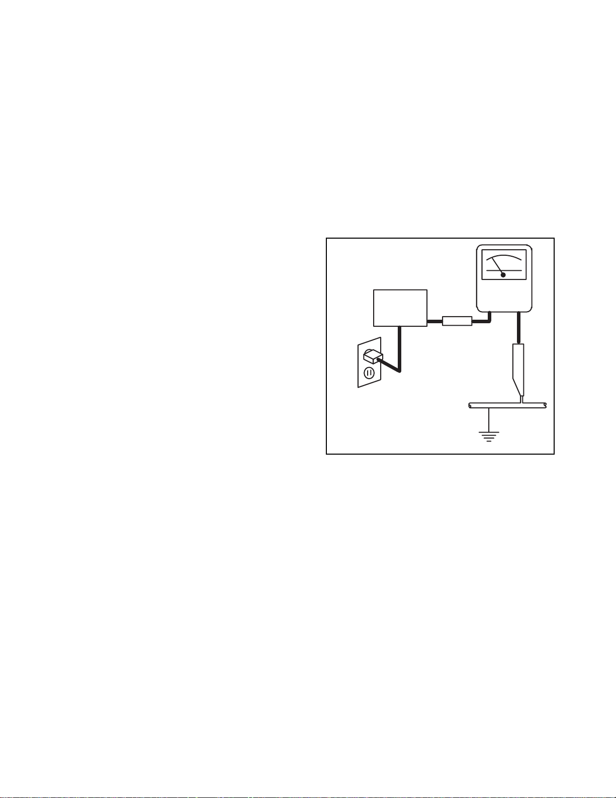
d. Leakage Current Hot Check - With the instrument
completely reassembled, plug the AC line cord
directly into a 120V AC outlet. (Do not use an
isolation transformer during this test.) Use a leakage
current tester or a metering system that complies
with American National Standards Institute (ANSI)
C101.1 Leakage Current for Appliances and
Underwriters Laboratories (UL) 1410, (50.7). With
the instrument AC switch first in the on position and
then in the off position, measure from a known earth
ground (metal water pipe, conduit, etc.) to all exposed
metal parts of the instrument (antennas, handle
brackets, metal cabinet, screw heads, metallic
overlays, control shafts, etc.), especially any exposed
metal parts that offer an electrical return path to the
chassis. Any current measured must not exceed 0.5
milli-ampere. Reverse the instrument power cord
plug in the outlet and repeat the test.
READING SHOULD
NOT BE ABOVE 0.5 mA
LEAKAGE
DEVICE
BEING
TESTED
TEST ALL EXPOSED
METAL SURFACES
ALSO TEST WITH
PLUG REVERSED
USING AC
ADAPTER PLUG
AS REQUIRED
ANY MEASUREMENTS NOT WITHIN THE LIMITS
SPECIFIED HEREIN INDICATE A POTENTIAL
SHOCK HAZARD THAT MUST BE ELIMINATED
BEFORE RETURNING THE INSTRUMENT TO THE
CUSTOMER OR BEFORE CONNECTING THE
ANTENNA OR ACCESSORIES.
e. X-Radiation and High Voltage Limits - Because
the picture tube is the primary potential source of Xradiation in solid-state TV receivers, it is specially
constructed to prohibit X-radiation emissions. For
continued X-radiation protection, the replacement
picture tube must be the same type as the original.
Also, because the picture tube shields and mounting
hardware perform an X-radiation protection function,
they must be correctly in place. High voltage must be
measured each time servicing is performed that
involves B+, horizontal deflection or high voltage.
Correct operation of the X-radiation protection circuits
also must be reconfirmed each time they are serviced.
(X-radiation protection circuits also may be called
"horizontal disable" or "hold down.") Read and apply
the high voltage limits and, if the chassis is so
equipped, the X-radiation protection circuit
CURRENT
TESTER
+
EARTH
GROUND
_
2-1
LCVISP
Page 5

specifications given on instrument labels and in the
Product Safety & X-Radiation Warning note on the
service data chassis schematic. High voltage is
maintained within specified limits by close tolerance
safety-related components/adjustments in the highvoltage circuit. If high voltage exceeds specified
limits, check each component specified on the chassis
schematic and take corrective action.
2. Read and comply with all caution and safety-related
notes on or inside the receiver cabinet, on the
receiver chassis, or on the picture tube.
3. Design Alteration Warning - Do not alter or add to
the mechanical or electrical design of this TV receiver.
Design alterations and additions, including, but not
limited to circuit modifications and the addition of
items such as auxiliary audio and/or video output
connections, might alter the safety characteristics of
this receiver and create a hazard to the user. Any
design alterations or additions will void the
manufacturer's warranty and may make you, the
servicer, responsible for personal injury or property
damage resulting therefrom.
4. Picture Tube Implosion Protection Warning - The
picture tube in this receiver employs integral implosion
protection. For continued implosion protection,
replace the picture tube only with one of the same
type number. Do not remove, install, or otherwise
handle the picture tube in any manner without first
putting on shatterproof goggles equipped with side
shields. People not so equipped must be kept safely
away while picture tubes are handled. Keep the
picture tube away from your body. Do not handle the
picture tube by its neck. Some "in-line" picture tubes
are equipped with a permanently attached deflection
yoke; because of potential hazard, do not try to
remove such "permanently attached" yokes from
the picture tube.
5. Hot Chassis Warning -
a. Some TV receiver chassis are electrically connected
directly to one conductor of the AC power cord and
maybe safety-serviced without an isolation
transformer only if the AC power plug is inserted so
that the chassis is connected to the ground side of
the AC power source. To confirm that the AC power
plug is inserted correctly, with an AC voltmeter,
measure between the chassis and a known earth
ground. If a voltage reading in excess of 1.0V is
obtained, remove and reinsert the AC power plug in
the opposite polarity and again measure the voltage
potential between the chassis and a known earth
ground.
b. Some TV receiver chassis normally have 85V
AC(RMS) between chassis and earth ground
regardless of the AC plug polarity. This chassis can
be safety-serviced only with an isolation transformer
inserted in the power line between the receiver and
the AC power source, for both personnel and test
equipment protection.
c. Some TV receiver chassis have a secondary ground
system in addition to the main chassis ground. This
secondary ground system is not isolated from the
AC power line. The two ground systems are
electrically separated by insulation material that
must not be defeated or altered.
6. Observe original lead dress. Take extra care to
assure correct lead dress in the following areas:a.
near sharp edges,b. near thermally hot parts-be
sure that leads and components do not touch
thermally hot parts,c. the AC supply,d. high voltage,
and,e. antenna wiring. Always inspect in all areas for
pinched, out of place, or frayed wiring. Check AC
power cord for damage.
7. Components, parts, and/or wiring that appear to
have overheated or are otherwise damaged should
be replaced with components, parts, or wiring that
meet original specifications. Additionally, determine
the cause of overheating and/or damage and, if
necessary, take corrective action to remove any
potential safety hazard.
8. Product Safety Notice - Some electrical and
mechanical parts have special safety-related
characteristics which are often not evident from
visual inspection, nor can the protection they give
necessarily be obtained by replacing them with
components rated for higher voltage, wattage, etc..
Parts that have special safety characteristics are
identified by a ( # ) on schematics and in parts lists.
Use of a substitute replacement that does not have
the same safety characteristics as the recommended
replacement part might create shock, fire, and/or
other hazards. The product's safety is under review
continuously and new instructions are issued
whenever appropriate. Prior to shipment from the
factory, our products are strictly inspected to confirm
they comply with the recognized product safety and
electrical codes of the countries in which they are to
be sold. However, in order to maintain such
compliance, it is equally important to implement the
following precautions when a set is being serviced.
2-2
LCVISP
Page 6
IMPORTANT SERVICE SAFETY PRECAUTION
T
M
H
Service work should be performed only by qualified service technicians who are
thoroughly familiar with all safety checks and the servicing guidelines which follow:
WARNING
1. For continued safety, no modification of any circuit
should be attempted.
2. Disconnect AC power before servicing.
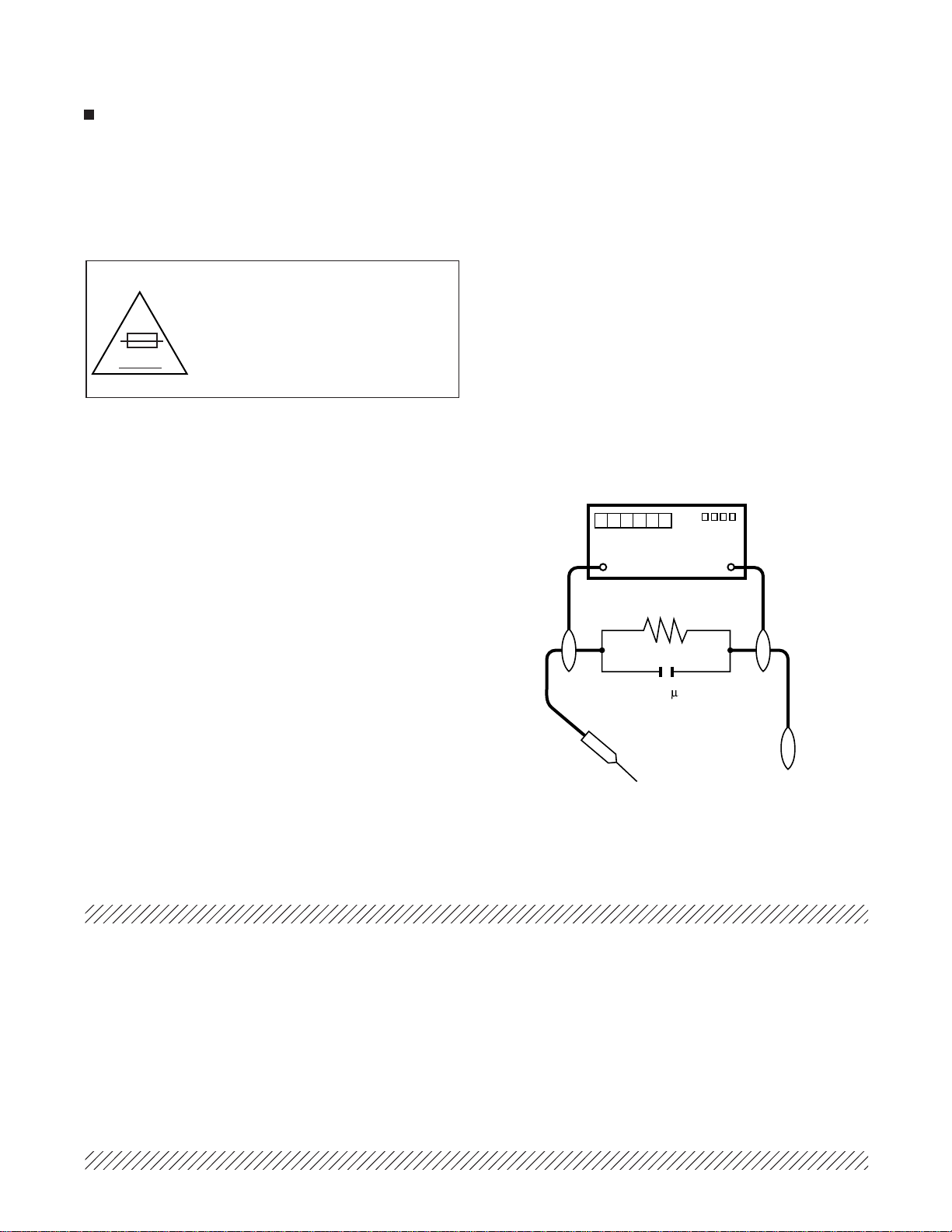
CAUTION: FOR CONTINUED
PROTECTION AGAINST A RISK OF
FIRE REPLACE ONL Y WITH SAME
TYPE F3701 (2.0A, 250V), F3702
A V
(1.25A, 250V), AND F6701 (6.3A,
250V) FUSE.
BEFORE RETURNING THE RECEIVER
(Fire & Shock Hazard)
Before returning the receiver to the user, perform
the following safety checks:
1. Inspect all lead dress to make certain that leads are
not pinched, and check that hardware is not lodged
between the chassis and other metal parts in the
receiver.
2. Inspect all protective devices such as non-metallic
control knobs, insulation materials, cabinet backs,
adjustment and compartment covers or shields,
isolation resistor-capacitor networks, mechanical
insulators, etc.
3. To be sure that no shock hazard exists, check for
leakage current in the following manner.
Plug the AC cord directly into a 110~240 volt AC
•
outlet, and connect the DC power cable into the
receiver’s DC jack. (Do not use an isolation
transformer for this test).
Using two clip leads, connect a 1.5k ohm, 10 watt
•
resistor paralleled by a 0.15µF capacitor in series
with all exposed metal cabinet parts and a known
earth ground, such as electrical conduit or electrical
ground connected to an earth ground.
Use an AC voltmeter having with 5000 ohm per volt,
•
or higher, sensitivity or measure the AC voltage drop
across the resistor.
Connect the resistor connection to all exposed metal
•
parts having a return to the chassis (antenna, metal
cabinet, screw heads, knobs and control shafts,
escutcheon, etc.) and measure the AC voltage drop
across the resistor.
All checks must be repeated with the AC cord plug
connection reversed. (If necessary, a nonpolarized
adaptor plug must be used only for the purpose of
completing these checks.)
Any reading of 0.75V peak (this corresponds to 0.5
mA. peak AC.) or more is excessive and indicates a
potential shock hazard which must be corrected
before returning the monitor to the owner.
DVM
AC SCALE
1.5k ohm
10W
0.15 F
TEST PROBE
O EXPOSED
ETAL PARTS
CONNECT TO
KNOWN EART
GROUND
SAFETY NOTICE
Many electrical and mechanical parts in LCD television
have special safety-related characteristics.
These characteristics are often not evident from visual
inspection, nor can protection afforded by them be
necessarily increased by using replacement components
rated for higher voltage, wattage, etc.
Replacement parts which have these special safety
characteristics are identified in this manual; electrical
components having such features are identified by “#”
and shaded areas in the Replacement Parts Lists and
Schematic Diagrams.
For continued protection, replacement parts must be
identical to those used in the original circuit.
The use of a substitute replacement parts which do not
have the same safety characteristics as the factory
recommended replacement parts shown in this service
manual, may create shock, fire or other hazards.
2-3
LCVISP
Page 7
PRECAUTIONS A PRENDRE LORS DE LA REPARATION
A
M
E
E
Ne peut effectuer la réparation qu’ un technicien spécialisé qui s’est parfaitement
accoutumé à toute vérification de sécurité et aux conseils suivants.
AVERTISSEMENT
1. N’entreprendre aucune modification de tout circuit.
C’est dangereux.
2. Débrancher le récepteur avant toute réparation.
PRECAUTION: POUR LA
PROTECTION CONTINUE
CONTRE LES RISQUES
D'INCENDIE, REMPLACER LE
A V
FUSIBLE P AR UN FUSIBLE DE
MEME TYPE F3701 (2.0A, 250V),
F3702 (1.25A, 250V) F6701 (6.3A,
250V).
VERIFICATIONS CONTRE L’INCEN-DIE
ET LE CHOC ELECTRIQUE
Avant de rendre le récepteur à l’utilisateur, effectuer
les vérifications suivantes.
1. Inspecter tous les faisceaux de câbles pour s’assurer
que les fils ne soient pas pincés ou qu’un outil ne soit
pas placé entre le châssis et les autres pièces
métalliques du récepteur.
2. Inspecter tous les dispositifs de protection comme
les boutons de commande non-métalliques, les
isolants, le dos du coffret, les couvercles ou blindages
de réglage et de compartiment, les réseaux de
résistance-capacité, les isolateurs mécaniques, etc.
3. S’assurer qu’il n’y ait pas de danger d’électrocution
en vérifiant la fuite de courant, de la facon suivante:
Brancher le cordon d’alimentation directem-ent à
•
une prise de courant de 110-240V. (Ne pas utiliser
de transformateur d’isolation pour cet essai).
A l’aide de deux fils à pinces, brancher une résistance
•
de 1.5kΩ 10 watts en parallèle avec un condensateur
de 0.15µF en série avec toutes les pièces métalliques
exposées du coffret et une terre connue comme une
conduite électrique ou une prise de terre branchée
à la terre.
Utiliser un voltmètre CA d’une sensibilité d’au moins
•
5000Ω/V pour mesurer la chute de tension en travers
de la résistance.
Toucher avec la sonde d’essai les pièces métalliques
•
exposées qui présentent une voie de retour au
châssis (antenne, coffret métallique, tête des vis,
arbres de commande et des boutons, écusson, etc.)
et mesurer la chute de tension CA en-travers de la
résistance.
Toutes les vérifications doivent être refaites après
avoir inversé la fiche du cordon d’alimentation. (Si
nécessaire, une prise d’adpatation non polarisée
peut être utilisée dans le but de terminer ces
vérifications.)
Tous les courants mesurés ne doivent pas dépasser
0,5 mA.
Dans le cas contraire, il y a une possibilité de choc
électrique qui doit être supprimée avant de rendre le
récepteur au client.
DVM
ECHELLE CA
1.5k ohm
10W
0.15 F
SONDE D'ESSAI
UX PIECES
ETALLIQUES
XPOSEES
BRANCHER A UN
TERRE CONNUE
AVIS POUR LA SECURITE
De nombreuses pièces, électriques et mécaniques,
dans les téléviseurs présentent des caractéristiques
spéciales relatives à la sécurité, qui ne sont souvent
pas évidentes à vue. Le degré de protection ne peut pas
être nécessairement augmentée en utilisant des pièces
de remplacement étalonnées pour haute tension,
puissance, etc.
Les pièces de remplacement qui présentent ces
caractéristiques sont identifiées dans ce manuel; les
pièces électriques qui présentent ces particularités
sont identifiées par la marque "#" et hachurées dans
la liste des pièces de remplacement et les diagrammes
schématiques.
Pour assurer la protection, ces pièces doivent être
identiques à celles utilisées dans le circuit d’origine.
L’utilisation de pièces qui n’ont pas les mêmes
caractéristiques que les pièces recommandées par
l’usine, indiquées dans ce manuel, peut provoquer des
électrocutions, incendies, radiations X ou autres
accidents.
2-4
LCVISP
Page 8

STANDARD NOTES FOR SERVICING
NOTE: CBA AND PWB MEANS PRINTED WIRING
BOARD.
Circuit Board Indications
a. The output pin of the 3 pin Regulator ICs is indicated
as shown.
Top View
Out
b. For other ICs, pin 1 and every fifth pin are indicated
as shown.
< Bottom View >
Input
In
Bottom View
5
Pin 1
10
c. The 1st pin of every male connector is indicated as
shown.
< Bottom View >
Pin 1
Instructions for Connectors
1. When you connect or disconnect the FFC (Flexible
Foil Connector) cable, be sure to first disconnect the
AC cord.
2. FFC (Flexible Foil Connector) cable should be inserted parallel into the connector, not at an angle.
Precautions for Using Lead-free Solder
1 Employing lead-free solder
Pb free mark (as shown below) indicates lead-free
solder, and is attached on the PWBs and service
manuals. For PWBs with Pb free mark, be sure to use
lead-free solder. For PWB without Pb free mark, use
standard solder. The alphabetical character following
Pb shows the type of lead-free solder.
2 Using lead-free wire solder
When fixing the PWB soldered with the lead-free solder,
apply lead-free wire solder. Repairing with conventional
lead wire solder may cause damage or accident due to
cracks.
As the melting point of lead-free solder (Sn-Ag-Cu) is
higher than the lead wire solder by 40°C, we recommend
you to use a dedicated soldering bit, if you are not
familiar with how to obtain lead-free wire solder or
soldering bit, contact our service station or service
branch in your area.
3 Soldering
As the melting point of lead-free solder (Sn-Ag-Cu) is
about 220°C which is higher than the conventional lead
solder by 40°C, and as it has poor solder wettability, you
may be apt to keep the soldering bit in contact with the
PWB for extended period of time. However, Since the
land may be peeled off or the maximum heat-resistance
temperature of parts may be exceeded, remove the bit
from the PWB as soon as you confirm the steady
soldering condition.
Lead-free solder contains more tin, and the end of the
soldering bit may be easily corroded. Make sure to turn
on and off the power of the bit as required.
If a different type of solder stays on the tip of the
soldering bit, it is alloyed with lead-free solder. Clean
the bit after every use of it.
When the tip of the soldering bit is blackened during
use, file it with steel wool or fine sandpaper.
FFC Cable
Connector
CBA
* Be careful to avoid a short circuit.
Be careful when replacing parts with polarity indication
on the PWB silk.
Lead-free wire solder for servicing
Part No. Description Code
ZHNDAi123250E J 0.3mm 250g(1roll) BL
ZHNDAi126500E J 0.6mm 500g(1roll) BK
ZHNDAi12801KE J 1.0mm 1kg(1roll) BM
3-1
LCV_NOTE
Page 9
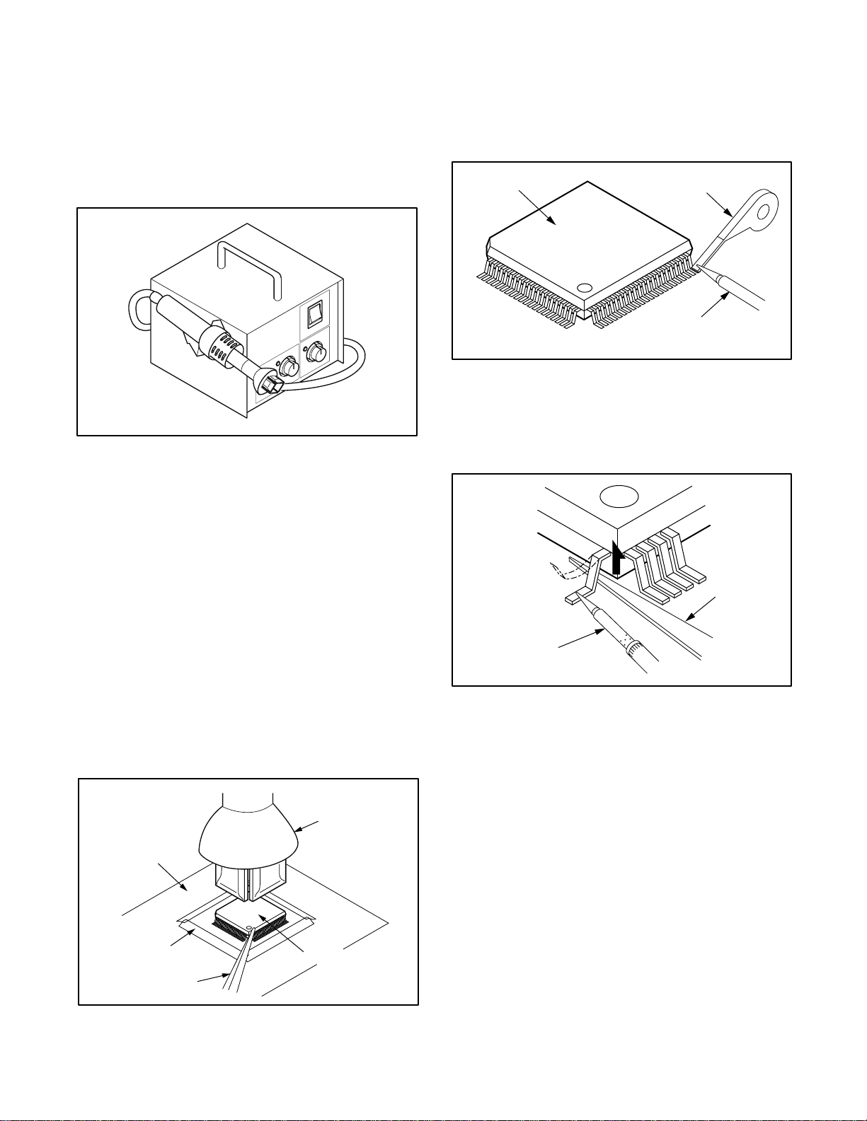
How to Remove / Install Flat Pack-IC
Flat Pack-IC
Desoldering Braid
Soldering Iron
Fig. S-1-3
Fine Tip
Soldering Iron
Sharp
Pin
Fig. S-1-4
With Soldering Iron:
1. Removal
With Hot-Air Flat Pack-IC Desoldering Machine:
(1) Prepare the hot-air flat pack-IC desoldering ma-
(2)Remove the flat pack-IC with tweezers while apply-
(3)Bottom of the flat pack-IC is fixed with glue to the
(4)Release the flat pack-IC from the CBA using twee-
Caution:
1. Do not supply hot air to the chip parts around the flat
2. The flat pack-IC on the CBA is affixed with glue, so
chine, then apply hot air to the Flat Pack-IC (about 5
to 6 seconds). (Fig. S-1-1)
Fig. S-1-1
ing the hot air.
CBA; when removing entire flat pack-IC, first apply
soldering iron to center of the flat pack-IC and heat
up. Then remove (glue will be melted). (Fig. S-1-6)
zers. (Fig. S-1-6)
pack-IC for over 6 seconds because damage to the
chip parts may occur. Put masking tape around the
flat pack-IC to protect other parts from damage.
(Fig. S-1-2)
be careful not to break or damage the foil of each pin
or the solder lands under the IC when removing it.
Hot-air
Flat Pack-IC
Desoldering
CBA
Masking
Tape
Tweezers
Machine
Flat Pack-IC
Fig. S-1-2
(1)Using desoldering braid, remove the solder from all
pins of the flat pack-IC. When you use solder flux
which is applied to all pins of the flat pack-IC, you can
remove it easily. (Fig. S-1-3)
(2)Lift each lead of the flat pack-IC upward one by one,
using a sharp pin or wire to which solder will not
adhere (iron wire). When heating the pins, use a fine
tip soldering iron or a hot air desoldering machine.
(Fig. S-1-4)
(3)Bottom of the flat pack-IC is fixed with glue to the
CBA; when removing entire flat pack-IC, first apply
soldering iron to center of the flat pack-IC and heat
up. Then remove (glue will be melted). (Fig. S-1-6)
(4)Release the flat pack-IC from the CBA using twee-
zers. (Fig. S-1-6)
With Iron Wire:
(1)Using desoldering braid, remove the solder from all
pins of the flat pack-IC. When you use solder flux
which is applied to all pins of the flat pack-IC, you can
remove it easily. (Fig. S-1-3)
(2) Affix the wire to a workbench or solid mounting point,
as shown in Fig. S-1-5.
(3)While heating the pins using a fine tip soldering iron
or hot air blower, pull up the wire as the solder melts
so as to lift the IC leads from the CBA contact pads
as shown in Fig. S-1-5.
3-2
LCV_NOTE
Page 10

(4)Bottom of the flat pack-IC is fixed with glue to the
Example :
Pin 1 of the Flat Pack-IC
is indicated by a " " mark.
Fig. S-1-7
Presolder
CBA
Flat Pack-IC
Fig. S-1-8
CBA; when removing entire flat pack-IC, first apply
soldering iron to center of the flat pack-IC and heat
up. Then remove (glue will be melted). (Fig. S-1-6)
(5)Release the flat pack-IC from the CBA using twee-
zers. (Fig. S-1-6)
Note:
When using a soldering iron, care must be taken to
ensure that the flat pack-IC is not being held by glue.
When the flat pack-IC is removed from the CBA,
handle it gently because it may be damaged if force
is applied.
Hot Air Blower
or
Iron Wire
2. Installation
(1)Using desoldering braid, remove the solder from the
foil of each pin of the flat pack-IC on the CBA so you
can install a replacement flat pack-IC more easily.
(2) The “
(3)Solder all pins of the flat pack-IC. Be sure that none
” mark on the flat pack-IC indicates pin 1. (See
Fig. S-1-7.) Be sure this mark matches the 1 on the
PCB when positioning for installation. Then presolder the four corners of the flat pack-IC. (See Fig. S1-8.)
of the pins have solder bridges.
To Solid
Mounting Point
CBA
Tweezers
Soldering Iron
Fig. S-1-5
Fine Tip
Soldeing Iron
Flat Pack-IC
Fig. S-1-6
3-3
LCV_NOTE
Page 11

Instructions for Handling
Semi-conductors
Electrostatic breakdown of the semi-conductors may
occur due to a potential difference caused by electrostatic
charge during unpacking or repair work.
1. Ground for Human Body
Be sure to wear a grounding band (1MΩ) that is properly
grounded to remove any static electricity that may be
charged on the body.
2. Ground for Workbench
Be sure to place a conductive sheet or copper plate with
proper grounding (1MΩ) on the workbench or other
surface, where the semi-conductors are to be placed.
Because the static electricity charge on clothing will not
escape through the body grounding band, be careful to
avoid contacting semi-conductors with your clothing.
< Incorrect >
< Correct >
CBA
Grounding Band
CBA
Conductive Sheet or
Copper Plate
3-4
LCV_NOTE
Page 12

CABINET DISASSEMBLY INSTRUCTIONS
e
NOTE: CBA AND PWB MEANS PRINTED WIRING
BOARD.
[ LC-15SH1U ]
1. Disassembly Flowchart
This flowchart indicates the disassembly steps to gain
access to item(s) to be serviced. When reassembling,
follow the steps in reverse order. Bend, route, and dress
the cables as they were originally.
[1] Rear Cabinet
[2] Main CBA
[6] Speaker L
[3] LCD Main CBA
[4] Liquid Crystal Panel
[5] Function CBA
[7] Speaker R
2. Disassembly Method
REMOVAL
ID/
LOC.
No.
[1]
[2] Main CBA
[3]
[4]
[5]
[6] Speaker L
PART
Rear
Cabinet
LCD Main D3D2
CBA
Liquid
Crystal
Panel
Function D3D2
CBA
REMOVE/*UNHOOK/
Fig.
UNLOCK/RELEASE/
No.
UNPLUG/DESOLDER
D1 6(S-1
D2
D3
D2
D3
D2
D3
), (
), 2(
6(S-4
*CN101A, *CN102A
*CN103A, *CN801
*CN802, *CN401
*CN402, *CN403
*CN404, *CN104
),
4(S-6
*CN311A, *CN321A
4(S-7
3(S-8
2(S-9
*CN310A
)
)
)
S-2
S-5
), (
),
S-3
Not
)
,
,
,
,
-
,
-
-
-
-
-
[8] Front Cabinet
[7] Speaker R
Front
[8]
Cabinet
↑↑↑ ↑ ↑
123 4 5
1 : Identification (location) No. of parts in the figures
2 : Name of the part
3 : Figure Number for reference
4 : Identification of parts to be removed, unhooked,
unlocked, released, unplugged, unclamped, or desoldered.
P=Spring, L=Locking Tab, S=Screw,
CN=Connector,
*=Unhook, Unlock, Release, Unplug, or Desolder
e.g.5(S-1) = five Screws (S-1),
2(L-2) = two Locking Tabs (L-2)
5 : Refer to "Reference Notes."
D2
D3
D2 ---------- -
2(S-10
)
-
4-1
L0270DC
Page 13
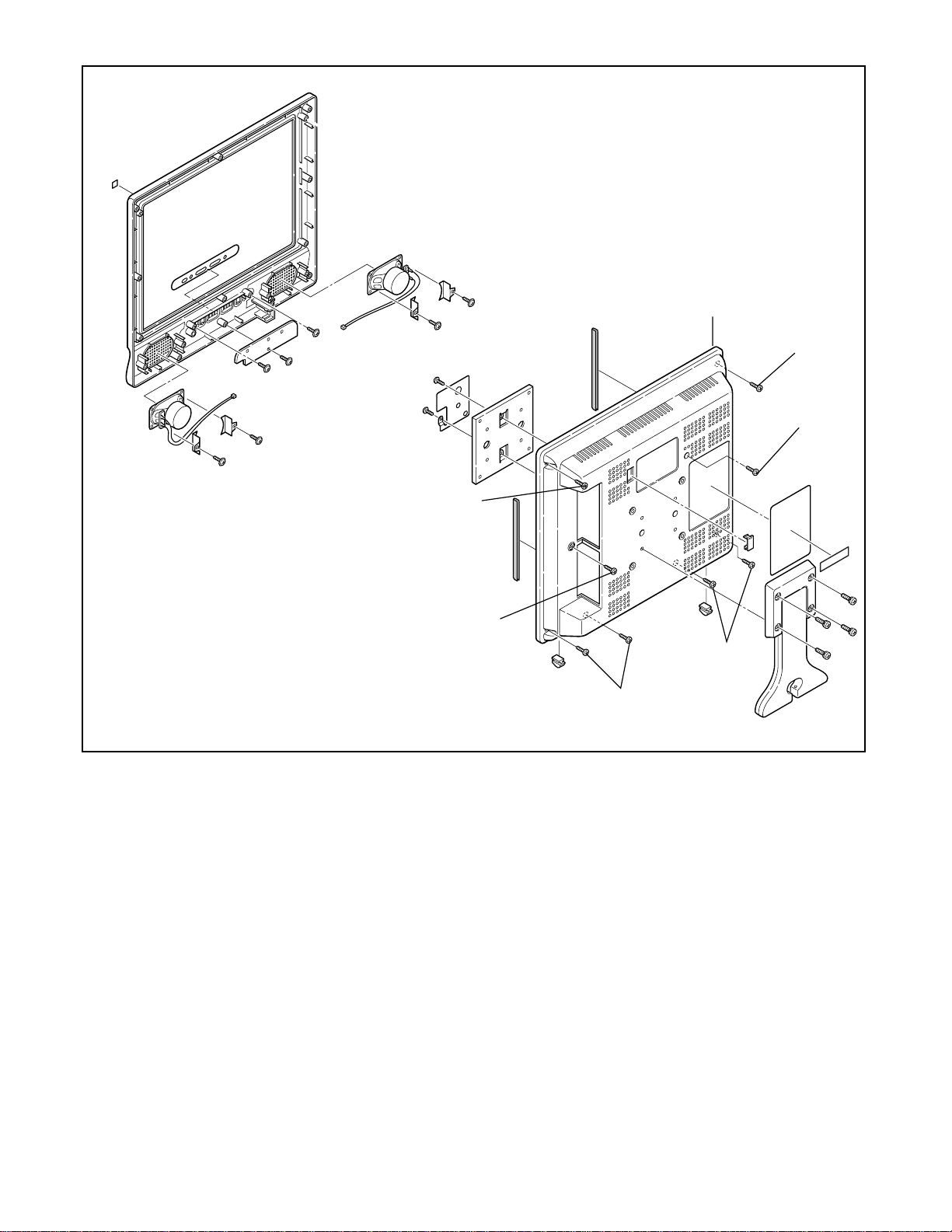
S-1
[1] Rear Cabinet
S-1
S-2
S-3
S-1
S-1
Fig. D1
4-2
L0270DC
Page 14

[8] Front Cabinet
[6] Speaker L
[7] Speaker R
S-8
[5] Function
CBA
S-10
[4] Liquid Crystal
Panel
S-9
S-7
S-9
S-7
S-7
S-6
S-4
[3] LCD Main CBA
[2] Main CBA
S-6
S-5
S-4
S-4
S-4
Fig. D2
4-3
L0270DC
Page 15

To Liquid Cristal Panel
CLN104
CN321A
LCD Main CBA
CN310A CN311A
CN113B CN112B
CN103A
CN102A CN101A
Function CBA
CN111B
CN104
CN401
CN402
To Liquid
Cristal Panel
CN403
Main CBA
CN801
To Speaker
CN404
CN802
To Speaker
Fig. D3
4-4
L0270DC
Page 16

[ LC-15AV1U ]
e
1. Disassembly Flowchart
This flowchart indicates the disassembly steps to gain
access to item(s) to be serviced. When reassembling,
follow the steps in reverse order. Bend, route, and dress
the cables as they were originally.
[1] Rear Cabinet
[2] Main CBA
[7] Speaker L
[3] LCD Main CBA
[4] Liquid Crystal Panel
[5] Function CBA
[6] IR Sensor CBA
[9] Front Cabinet
[8] Speaker R
ID/
LOC.
PART
No.
Rear
[1]
Cabinet
[2] Main CBA
LCD Main D6D5
[3]
CBA
Liquid
[4]
Crystal
Panel
Function D6D5
[5]
CBA
IR Sensor D6D5
[6]
CBA
[7] Speaker L
REMOVAL
REMOVE/*UNHOOK/
Fig.
UNLOCK/RELEASE/
No.
UNPLUG/DESOLDER
6(S-4
), (
), 2(
S-2
S-5
D4 9(S-1
*CN101A, *CN102A
*CN103A, *CN801
D5
*CN802, *CN401
D6
*CN402, *CN403
*CN404, *CN104,
*CN105
),
4(S-6
*CN310A
*CN311A, *CN321A
D5
D6
D5
D6
4(S-7
3(S-8
2(S-9
2(S-10
)
)
)
)
), (
),
S-3
Not
)
-
,
,
,
-
,
,
-
-
-
-
-
[8] Speaker R
Front
[9]
Cabinet
D5
D6
D5 ---------- -
2(S-11
)
-
↑↑↑ ↑ ↑
123 4 5
1 : Identification (location) No. of parts in the figures
2 : Name of the part
3 : Figure Number for reference
4 : Identification of parts to be removed, unhooked,
unlocked, released, unplugged, unclamped, or desoldered.
P=Spring, L=Locking Tab, S=Screw,
CN=Connector,
*=Unhook, Unlock, Release, Unplug, or Desolder
e.g.5(S-1) = five Screws (S-1),
2(L-2) = two Locking Tabs (L-2)
5 : Refer to "Reference Notes."
4-5
L0270DC
Page 17

[1] Rear Cabinet
S-1
S-1
S-3
S-1
S-2
S-1
S-1
S-1
Fig. D4
4-6
L0270DC
Page 18
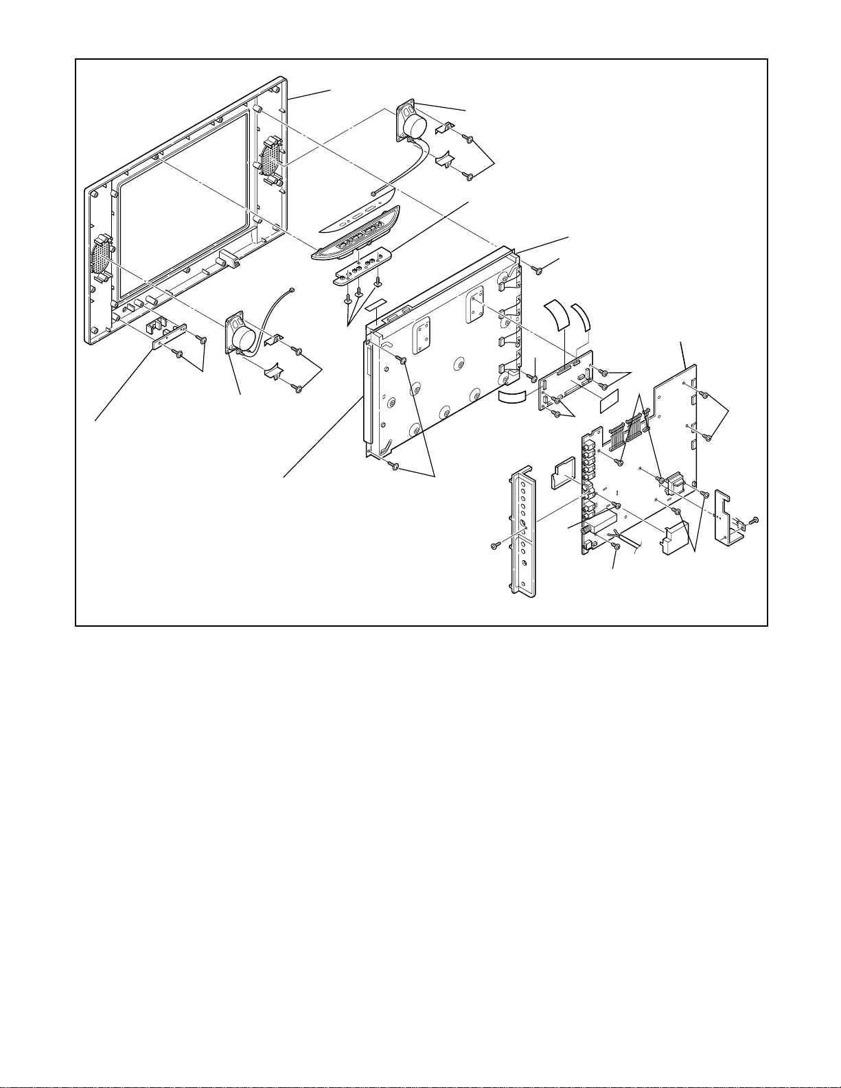
[9] Front Cabinet
[7] Speaker L
S-10
[5] Function CBA
[3] LCD Main CBA
S-7
S-9
[6] IR Sensor CBA
S-8
S-11
[8] Speaker R
[4] Liquid Crystal
Panel
S-7
S-7
S-4
S-6
[2] Main CBA
S-6
S-5
S-4
S-4
S-4
Fig. D5
4-7
L0270DC
Page 19

To Liquid Cristal Panel
CLN104A
CN321A
LCD Main CBA
CN310A CN311A
CN113B CN112B
CN103A
CN102A CN101A
Function CBA
CN111B
CN104A
CN401
CN402
To Liquid
Cristal Panel
CN403
Main CBA
CN801 CN105
To Speaker
CLN105
IR Sensor CBA
CN404
CN802
To Speaker
Fig. D6
4-8
L0270DC
Page 20
ELECTRICAL ADJUSTMENT INSTRUCTIONS
NOTE: CBA AND PWB MEANS PRINTED WIRING
BOARD.
NOTE:
Electrical adjustments are required after replacing circuit
components and certain mechanical parts. It is important
to perform these adjustments only after all repairs and
replacements have been completed.
Also, do not attempt these adjustments unless the
proper equipment is available.
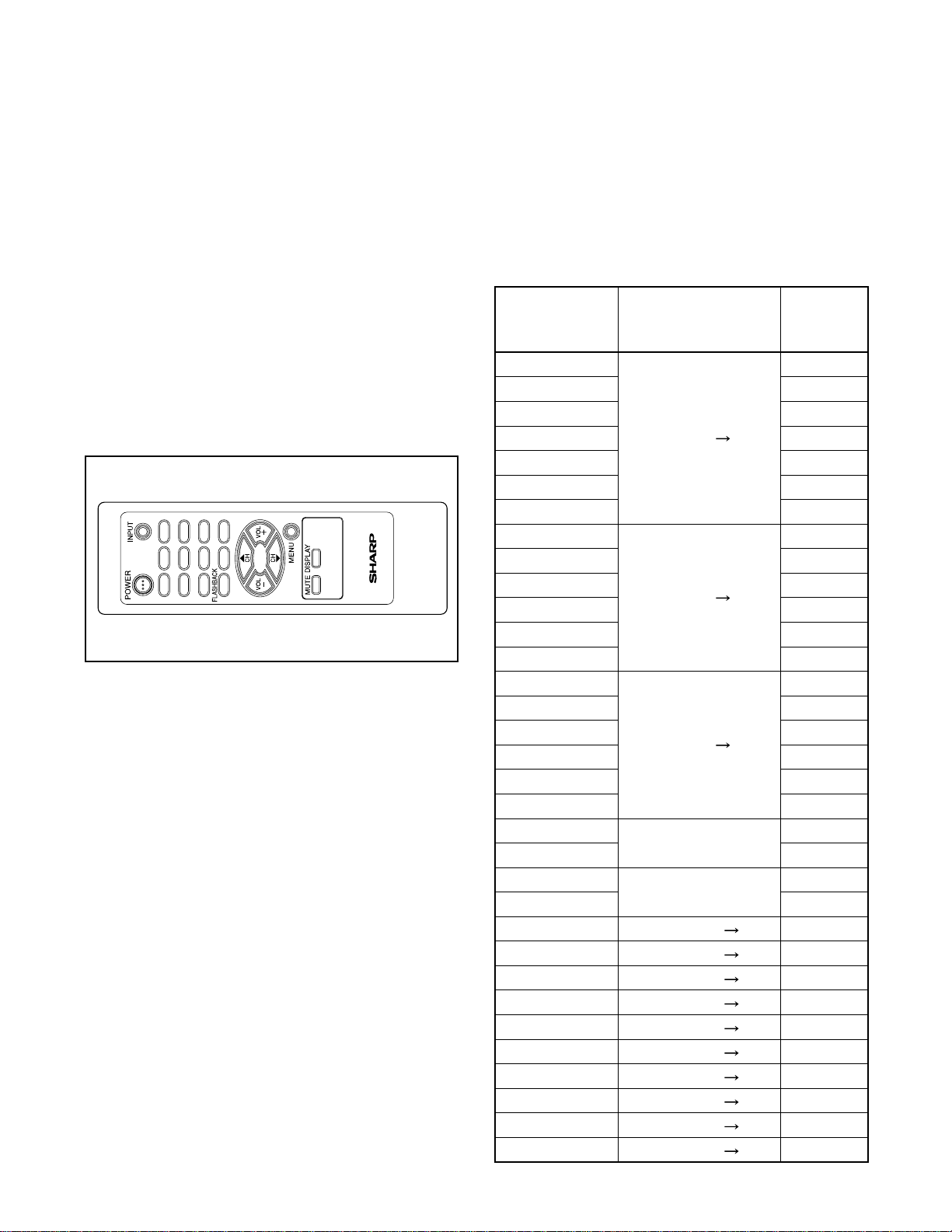
Test Equipment Required
1. NTSC Pattern Generator (Color Bar W/White Window, Red Color, Dot Pattern, Gray Scale,
Monoscope, Multi-Burst)
2. Remote control unit (attached remote control unit)
9
100
0
56
123
4
78
LCDTV
3. Color Analyzer
4. DC Voltmeter
How to set up the service mode:
Service mode:
1. Turn the power on. (Use main power on the TV unit.)
2. In standby mode, simultaneously press “POWER”
button and “MENU” button on the TV unit. Version of
micro computer will display on the LCD or display.
(Ex: 0001AGP-0.11, 0002AGP-0.14 or 0003AGP-
0.17)
1. Initial Setting
General
Enter the Service mode.
Set the each initial data as shown on table 1 below.
Table 1: Initial Data
BUTTON
(
ITEM
on the service
remote control
)
BRT
CNT 185
CLR-R 72
CLR-B 72
MENU
1
TNT 56
V-TNT 65
SHR 28
S-BRT
S-CNT 185
S-CLR-R 72
S-CLR-B 72
MENU
2
S-TNT 65
S-SHR 28
C-BRT
C-CNT 185
C-CLR-R 67
C-CLR-B 73
MENU
3
C-TNT 72
C-SHR 28
SAIDO
C-SAIDO 143
NORMAL
DARK 150
COR(C/D1
COG(C/D1
COB(C/D1
DR(C/D1
DG(C/D1
DB(C/D1
C-COR(C/D2
C-COG(C/D2
C-COB(C/D2
C-DR(C/D2
)
)
)
)
)
)
)
)
)
)
5
0
Vol down 1 512
Vol down 2 512
Vol down 3 512
Vol down 4 130
Vol down 5 132
Vol down 6 117
Vol down 1 512
Vol down 2 512
Vol down 3 512
Vol down 4 130
DATA
VALUE
126
126
126
148
74
5-1
L0270EA
Page 21
BUTTON
(
ITEM
C-DG(C/D2
C-DB(C/D2
7F
LANGUAGE SPA/FRA
STEREOTYP MTS
ACCESSCODE
BLACKLIGHT ON
HD OFF
HRD OFF
NCM OFF
ASPECT OFF
)
)
on the service
remote control
Vol down 5 132
Vol down 6 117
Vol down
)
DATA
VALUE
FF
ON
3. Flicker Adjustment
Note: Use remote control unit
1. Enter the Service mode. (See page 5-1)
2. Press “2” button on the remote control unit.
The following screen appears.
2. +B Adjustment
Purpose: To obtain correct operation.
Symptom of Misadjustment: The picture is dark and
the unit does not operate correctly.
Test point Adj. Point Mode Input
TP401(B+)
TP300(GND)
M. EQ.
DC Voltmeter
Note: TP401, TP300(GND), VR601 --- Main CBA
1. Connect DC Volt Meter to TP401 and TP300(GND).
2. Adjust VR601 so that the voltage of TP401 becomes
+13.0±0.5V DC.
VR601
--- ---
Spec.
+13.0±0.5V DC.
3. If Flicker Adjustment is not fit, the screen become the
following.
FLASH
(Go and Off)
4. Press “CH o/p” buttons on the remote control unit
until flash stops.
4. TV Reset to Default
To reset software, press “5” button on the remote
control unit for at least 5 seconds after pressing
“FLASHBACK” button on the remote control unit.
5-2
L0270EA
Page 22

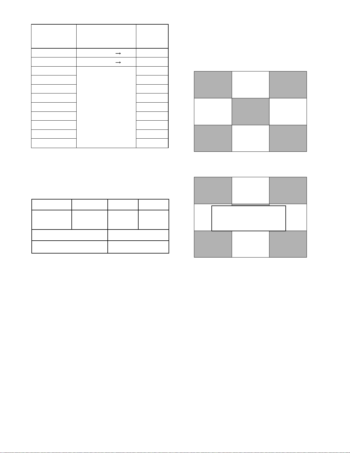
The following adjustment normally are not attempted
Test point Adj. Point Mode Input
Screen
M. EQ.
Spec.
Pattern Generator,
Color analyzer
x (0.282 to 0.302)
y (0.297 to 0.317)
Figure
VIDEO 1
VIDEO 2
White Purity
(APL 80%
and 40%)
APL
80%
x (0.276 to 0.296)
y (0.289 to 0.309)
APL
40%
Color Analyzer
It carries out in a darkroom.
L = 50 cm
Perpendicularity
INPUT: WHITE 80%
Fig. 2
CH
buttons
in the field. Only when replacing the LCD Panel then
adjust as a preparation.
5. White Balance Adjustment
Purpose: To mix red, green and blue beams correctly
for pure white.
Symptom of Misadjustment: White becomes bluish
or reddish.
Method 1
Vary the “RCUTOFF”, “BCUTOFF”, “RGAIN” and
“BGAIN” settings of the adjustment process below.
Adjustment Process
Method 2
RCUTOFF
GCUTOFF
BCUTOFF
R-GAIN
G-GAIN
B-GAIN
1. Receive the black signal (white 40%).
Adjust the “RCUTOFF” and “BCUTOFF” settings to
have the black color temperature as specified.
2. Receive the white 80% signal.
Adjust two of the “R-GAIN”, “G-GAIN” and “B-GAIN”
settings in the decreasing direction to be visible
white.
Note: Make sure at least one of the “R-GAIN”, “GGAIN” and “B-GAIN” settings is “0”.
3. Check to see if the black and white color temperatures are as specified. If not, repeat the above steps
1 and 2.
0
Red cut - off adjustment
0
Green cut - off adjustment
0
Blue cut - off adjustment
0
White balance
0
White balance
0
White balance
Note: Use remote control unit
1. Operate the unit for more than 20 minutes.
2. Input the White Purity (APL 80%).
3. Set the color analyzer to the CHROMA mode and
bring the optical receptor to the center on the LCDPanel surface after zero point calibration as shown
above.
Note: The optical receptor must be set perpendicularly to the LCD Panel surface.
4. Enter the Service mode. Press “VOL p” button on
the remote control unit and select “C/D” mode.
5. When “x” value and “y” value are not within specification, adjust “DB” or “DR”. Refer to “1. Initial Setting.”
6. Input the White Purity (APL 40%).
7. Press “VOL p” button on the remote control unit and
select “C/D” mode.
8. When “x” value and “y” value are not within specification, adjust “COB” or “COR”. Refer to “1. Initial
Setting.”
9. Also VIDEO 2 mode.
5-3
L0270EA
Page 23

6. Sub-Brightness Adjustment
Purpose: To mix red, green and blue beams correctly
for pure white.
Symptom of Misadjustment: White becomes bluish
or reddish.
Confirmation at [VIDEO-1]
1. Set CG951 to 7/5/3 IRE 3-step grayscale.
7 IRE 5 IRE 3 IRE
TEST PATTERN (7/5/3 IRE)
2. Apply CG951 video signal to VIDEO1 input.
3. Enter the Service mode.
4. Make sure that contrast and brightness controls are
set to initial position.
5. Confirm “5 IRE” position was biginning to bright.
6. If “5 IRE” position was bigining to bright, no need to
adjust.
7. If “5 IRE” position is not avilable or to be highly
brightness, then adjust the following values by using
remote control unit. Refer to “1. Initial Setting.”
RF/VIDEO1: BRT
VIDEO2: C-BRT
Confirmation at [VIDEO-2]
1. Set CG951 to 7/5/3 IRE 3-step grayscale.
2. Apply CG951 video signal to “Y” input.
3. Enter the Service mode.
4. Make sure that contrast and brightness controls are
set to initial position.
5. Confirm “5 IRE” position was beginning to bright.
6. If “5 IRE” position was beginning to bright, no need
to adjust.
7. If “5 IRE” position is not available or to be highly
brightness, then adjust the following values by using
remote control unit. Refer to “1. Initial Setting.”
RF/VIDEO1: BRT
VIDEO2: C-BRT
5-4
L0270EA
Page 24

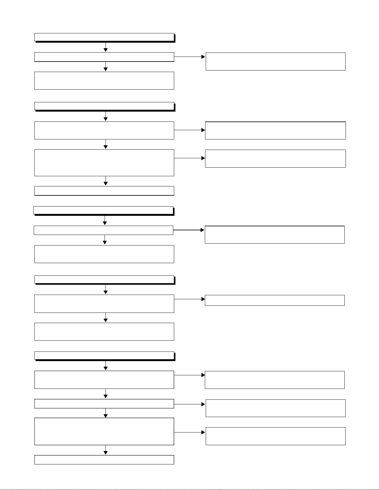
TROUBLESHOOTING
Table of Contents for the Troubleshooting Flow Charts
Flow
Chart
No.
1 The power cannot be turned on. 6-2
2 The fuse blows out. 6-2
3 When the output voltage fluctuates. 6-2
4 When buzz sound can be heard in the vicinity of power circuit. 6-2
5 AL-8V is not outputted. 6-2
6 AL+3.3V is not outputted. 6-3
7 AL+40V is not outputted. 6-3
8 AL+5V is not outputted. 6-3
9 AL+33V is not outputted. 6-3
10 AL+12V is not outputted. 6-3
11 REG+5V(1) is not outputted. 6-4
12 REG+5V(2) is not outputted. 6-4
13 P-ON+3.3V(D) is not outputted. 6-4
14 P-ON+3.3V(A) is not outputted. 6-4
15 P-ON+1.8V(D) is not outputted. 6-4
16 PANEL+24V is not outputted. 6-5
17 PANEL+5.4V is not outputted. 6-5
18 PANEL-12V is not outputted. 6-5
19 PANEL+12V is not outputted. 6-5
20 PANEL+9V is not outputted. 6-5
21 The key operation is not functioning. 6-6
22 No operation is possible from the remote control unit. 6-6
Picture does not appear normally. (Tuner input / Video input/S-Video input.
23
24 Picture does not appear normally. (Y / Pb / Pr input.
25 Audio is not outputted normally. (Tuner input.
26 Audio is not outputted normally. (Audio input terminals.
Description Page
)
)
)
)
6-7
6-7
6-8
6-8
NOTE: CBA AND PWB MEANS PRINTED WIRING
BOARD.
6-1
L0370TS
Page 25

1. POWER SUPPLY SECTION
F
FLOW CHART NO.1
The power cannot be turned on.
Is the fuse (F601) normal?
Yes
Is normal state restored when once unplugged
power cord is plugged again several seconds?
Yes
Is the AL +3.3V line voltage normal?
Yes
Check each rectifying circuit of the secondary
circuit and service it if defective.
FLOW CHART NO.2
The fuse blows out.
Check the presence that the primary component
is leaking or shorted and service it if defective.
After servicing, replace the fuse.
FLOW CHART NO.3
When the output voltage fluctuates.
No
No
No
See FLOW CHART No.2 <The fuse blows out.>
Check if there is any leak or short-circuiting on the
primary circuit component, and service it if defective.
(Q601,Q603.T601,D605,D606,D607,D608,C605,
C606,C610,C654)
Check the presence that the rectifying diode or circuit
is shorted in each rectifying circuit of secondary side,
and service it if defective.
Does the photocoupler circuit on the
secondary side operate normally?
Yes
Check IC601,D612,D613,D615 and their periphery,
and service it if defective.
FLOW CHART NO.4
When buzz sound can be heard in the vicinity of power circuit.
Check if there is any short-circuit on the rectifying diode and the circuit in each rectifying circuit of the secondary side,
and service it if defective. (IC603,IC604,D630,D631,D632,D633,D635,D645)
LOW CHART NO.5
AL-8V is not outputted.
Is approximately -8V voltage supplied to the
anode of D631?
Check if their is any leak or short-circuit on the
loaded circuit, and service it if defective.
Yes
No
No
Check IC601,D646,D649 and their periphery, and
service it if defective.
Check D631 and the periphery circuit, and service
it if defective.
6-2
L0370TS
Page 26
FLOW CHART NO.6
F
AL+3.3V is not outputted.
Is 3.3V voltage supplied to the cathode of D514?
Yes
Check if there is any leak or short-circuit on
the loaded circuit and service it if defective.
FLOW CHART NO.7
AL+40V is not outputted.
Is approximately 40V voltage supplied to the
emitter of Q516?
Yes
Is the voltage of base on Q516 lower than the
voltage of emitter on Q516 when turning
the power on?
Yes
Replace Q516.
LOW CHART NO.8
AL+5V is not outputted.
Is 5V voltage supplied to the cathode of D633?
Yes
Check if there is any leak or short-circuit on
the loaded circuit and service it if defective.
No
No
No
No
Check D635,C637 and their periphery circuit, and
service it if defective.
Check D645,D646,C644 and their periphery circuit,
and service it if defective.
Check Q517 and P-ON-H line, and service it if
defective.
Check D633,C635 and their periphery circuit, and
service it if defective.
FLOW CHART NO.9
AL+33V is not outputted.
Is approximately 40V voltage supplied to the
emitter of Q516?
Yes
Check D641,C648,C649,R658 and their
periphery circuit, and service it if defective.
FLOW CHART NO.10
AL+12V is not outputted.
Is approximately 12V voltage supplied to the
cathode of D630?
Yes
Is 12V voltage supplied to the emitter of Q427?
Yes
Is the voltage of base on Q427 lower than the
voltage of emitter on Q427 when turning
the power on?
Yes
Replace Q427.
No
No
No
No
See FLOW CHART No.7
Check D630,D632 and their periphery circuit, and
service it if defective.
Check C634,C636,L630 and their periphery circuit,
and service it if defective.
Check Q401 and BACKLIGHT-SW line, and
service it if defective.
6-3
L0370TS
Page 27

F
LOW CHART NO.11
F
F
F
F
REG+5V(1) is not outputted.
Is approximately 12V voltage supplied to Pin(1) of
IC604?
Check IC604,C603 and their periphery circuit,
and service it if defective.
LOW CHART NO.12
REG+5V(2) is not outputted.
Is 7.4V voltage supplied to Pin(1) of IC603?
Check IC603,C673 and their periphery circuit,
and service it if defective.
LOW CHART NO.13
P-ON+3.3V(D) is not outputted.
Is approximately 4.7V voltage supplied to
Pin(1) of IC502?
Yes
Yes
No
No
No
See FLOW CHART No.9
See FLOW CHART No.8
See FLOW CHART No.6
Check IC502,IC505 and there periphery circuit
service and it if defective.
LOW CHART NO.14
P-ON+3.3V(A) is not outputted.
Is 4.7V voltage supplied to Pin(1) of IC504?
Check IC504 and the periphery circuit, and
service it if defective.
LOW CHART NO.15
P-ON+1.8V(D) is not outputted.
Is 3.5V voltage supplied to Pin(1) of IC503?
Check IC503 and the periphery circuit, and
service it if defective.
Yes
Yes
Yes
No
No
See FLOW CHART No.6
See FLOW CHART No.6
6-4
L0370TS
Page 28

F
LOW CHART NO.16
F
F
F
F
PANEL+24V is not outputted.
Is approximately 40V voltage supplied to the
collector of Q501?
Yes
Check Q501,Q502,Q511 and their periphery
circuit, and service it if defective.
LOW CHART NO.17
PANEL+5.4V is not outputted.
Is approximately 12V voltage supplied to the
collector of Q503?
Yes
Check Q503,Q504,Q514 and their periphery
circuit, and service it if defective.
LOW CHART NO.18
PANEL-12V is not outputted.
No
See FLOW No.7
No
See FLOW No.10
Is approximately -8V voltage supplied to the
emitter of Q505?
Yes
Check Q505 and the periphery circuit, and
service it if defective.
LOW CHART NO.19
PANEL+12V is not outputted.
Is approximately 12V voltage supplied to the
collector of Q515?
Yes
Check Q515,Q516,Q517 and their periphery
circuit, and service it if defective.
LOW CHART NO.20
PANEL+9V is not outputted.
No
See FLOW No.5
No
See FLOW No.10
Is approximately 12V voltage supplied to Pin(1)
of IC506?
Yes
Check IC506 and their periphery circuit, and
service it if defective.
No
6-5
See FLOW No.19
L0370TS
Page 29

F
LOW CHART NO.21
F
The key operation is not functioning.
Are the contact point and installation state of the key
switches (SW101,SW102,SW103,SW104,SW105,
SW107,SW116) normal?
Yes
When pressing each switches (SW101,SW102,
SW103,SW104,SW105,SW107,SW116) do the
voltage of each pin of CN102A (shown below)
increase?
SW101,102,103,104,105,107 : CN102A PIN 6
SW116 : CN102A PIN 7
Yes
Replace LCD MAIN CBA UNIT.
LOW CHART NO.22
No operation is possible from the remote control unit.
Operation is possible from the remote control unit.
Yes
Is 3.3 voltage supplied to Pin(3) terminal of the
infrared remote control receiver (RCV101)?
No
No
No
Re-install the switches (SW101,SW102,SW103,
SW104,SW105,SW107,SW116) correctly or replace
the poor switch.
Check the switches (SW101,SW102,SW103,SW104,
SW105,SW107,SW116) and their periphery, and
service it if defective.
Check P-ON+3.3V(D) line and service it if defective.
Yes
Is the "L" pulse sent out Pin(1) terminal of receiver
(RCV101) when the infrared remote control is
activated?
Yes
Is the "L" pulse supplied to the Pin(1) of CN102A?
Yes
Replace LCD MAIN CBA UNIT.
No
No
Replace the infrared remote control receiver
(RCV101) or the remote control unit.
Check the line between Pin(1) terminal of receiver
(RCV101) and Pin(1) of CN102A , and service
it if defective.
6-6
L0370TS
Page 30

2. VIDEO SIGNAL SECTION
FLOW CHART NO.23
Picture does not appear normally. (Tuner input / Video input/S-Video input.)
Are the video signals inputted to the specific
input terminal?
Are the luminance signals inputted to the
Pin(1) of IC781?
Are the chrominance signals inputted to the
Pin(13) of IC781?
Are the component video signals inputted to the
Pin(5) of IC781?
Are the component video signals inputted to the
Pin(3) of IC781?
Yes
Are the video signals outputted to the specific
output terminal?
Are the luminance signals outputted to the
Pin(15) of IC781?
Are the chrominance signals outputted to the
Pin(14) of IC781?
Are the component video signals inputted to the
Pin(4) of IC781?
Yes
Are the video signals outputted to the specific
output terminal?
Are the luminance signals outputted to the
Pin(9) of CN103A?
Are the chrominance signals outputted to the
Pin(7 of CN103A?
Are the component video signals inputted to the
Pin(11) of CN103A?
Yes
No
No
No
No
No
No
No
No
No
No
Check the line between each pin of IC781 and input
terminal and service it if defective.
Check the line between Pin(1) of IC781 and JK721,
and service it if defective.
Check the line between Pin(13) of IC781 and JK721,
and service it if defective.
Check the line between Pin(5) of IC781 and JK722,
and service it if defective.
Check the line between Pin(3) of IC781 and TU1,
and service it if defective.
Check IC781 and the periphery circuit,
and service it if defective.
Check the line between each pin of IC781 and CN103A
and service it if defective.
Check the line between Pin(15) of IC781 and Pin(9)
of CN103A, and service it if defective.
Check the line between Pin(14) of IC781 and Pin(7)
of CN103A, and service it if defective.
Check the line between Pin(4) of IC781 and Pin(11)
of CN103A, and service it if defective.
Replace LCD MAIN CBA UNIT or LCD MODULE.
FLOW CHART NO.24
Picture does not appear normally. (Y / Pb / Pr input.)
Are the video signals outputted to the specific
input terminal?
Are the Y signals outputted to the Pin(5) of
CN103A?
Are the Pb signals outputted to the Pin(3) of
CN103A?
Are the Pr signals outputted to the Pin(1) of
CN103A?
Yes
Replace LCD MAIN CBA UNIT or LCD MODULE.
No
No
No
6-7
Check the line between each input terminal and CN103A
and service it if defective.
Check the line between JK726 and Pin(5)
of CN103A, and service it if defective.
Check the line between JK727 and Pin(3)
of CN103A, and service it if defective.
Check the line between JK728 and Pin(1)
of CN103A, and service it if defective.
L0370TS
Page 31

3. AUDIO SIGNAL SECTION
F
FLOW CHART NO.25
Audio is not outputted normally. (Tuner input.)
Are the SIF signal inputted to the Pin(21) of IC851?
Yes
Are the audio(L/R) signal inputted to the Pin(4,11) of
IC852?
Yes
Are the audio(L/R) signal outputted to the Pin(3,13) of
IC852?
Yes
Are the audio(L/R) signal outputted to the Pin(11,14) of
IC801?
Yes
Check SP801,SP802,JK801 and their periphery circuit,
and service it if defective.
LOW CHART NO.26
Audio is not outputted normally. (Audio input terminals.)
No
No
No
No
Check TU1,SF,IC11,CF32 and their periphery circuit,
and service it if defective.
Check IC851 and the periphery circuit,
and service it if defective.
Check IC852 and the periphery circuit,
and service it if defective.
Check IC801 and the periphery circuit,
and service it if defective.
Are the audio(L/R) signal inputted to the Pin(1,2,12,15)
of IC852?
Yes
Are the audio(L/R) signal outputted to the Pin(3,13) of
IC852?
Yes
Are the audio(L/R) signal outputted to the Pin(11,14) of
IC801?
Yes
Check SP801,SP802,JK801 and their periphery circuit,
and service it if defective.
No
No
No
Check the line between Pin(1,2,12,15) of IC852 and
each Audio input terminals (JK723,JK724,JK729,JK730),
and service it if defective.
Check IC852 and the periphery circuit,
and service it if defective.
Check IC801 and the periphery circuit,
and service it if defective.
6-8
L0370TS
Page 32

BLOCK DIAGRAMS
System Control Block Diagram
POWER
D101
P-ON+3.3V
Q101
SENSOR
KEY SWITCH
REMOTE
KEY SWITCH
RCV101
KEY-IN122
KEY-IN211
RCV-IN55
P-ON-H66
CN104 CLN104
KEY-IN118 6
KEY-IN217 7
RCV-IN23 1
CN112B CN102A
FUNCTION CBA
LC-15SH1U
POWER
D102
P-ON+3.3V
Q102
SENSOR
REMOTE
RCV102
CLN105CN105
RCV-IN33
P-ON-H44
LC-15AV1U
TO
LCD BLOCK
DIAGRAM
TO POWER SUPPLY
BLOCK DIAGRAM
TO AUDIO
VGH-H
A-MUTE
VOLUME
VOLUME15 9
CN112B CN102A
BLOCK DIAGRAM
P-ON-H
A-MUTE13 11
SDA
WF1
TO LCD BACKLIGHT
BLOCK DIAGRAM
IR SENSOR CBA
P-ON-H
PROTECT-1
PROTECT-2
PROTECT-1
BACKLIGHT-SW
BACKLIGHT-ADJ
BACKLIGHT-SW
VGH-H321
19 5
CN112B CN102A
BACKLIGHT-ADJ
21 3
P-ON-H16 8
PROTECT-1915
PROTECT-2816
CN112B CN102A
SCL
INPUT-0
INPUT-1
INPUT-012 12
CN112B CN102A
TO IF/VIDEO
BLOCK DIAGRAM
SCL
SDA
S-SW
INPUT-111 13
S-SW717
SCL618
SDA519
WF3
WF2
TO POWER SUPPLY
PROTECT-3
PROTECT-310 14
CN113B CN103A
BLOCK DIAGRAM
MAIN CBA
IC333
(TV MICRO CONTROLLER)
3
KEY-IN1
4
KEY-IN2
VREF(0)
VREF(1)
VREF(3)
VREF(5)
VREF(7)
VREF(8)
VREF(10)
VREF(11)
V-COM
V-COM
DRIVE
15 16
14 13
4
8
5
VCC
6
IC161
16
OUTCON
Q253,Q254
+3.3V
RESET
4 5
21
RESET
PANEL+5.4V
RESET
Q161
LCD MAIN CBA UNIT
3.3V<-->5V
CONVERTER
Q121
6
7
22
18
17
PROTECT-1
BACKLIGHT-ADJ
20353140193241
P-ON-H
A-MUTE
VOLUME
PROTECT-2
INPUT-0
12
VGH-H
BACKLIGHT-SW
8
23
+5V
SCL
SDA
S-SW
INPUT-1
BUS-OPEN
PROTECT-3
IC181
(MEMORY)
7
WP
6
5
SCL
SDA
CN115(NO CONNECTION)
SDA 2
SCL 1
BUS-OPEN 4
26
25
(PWM CONTROL)
IC202
X171
27MHz
42
43
11
XIN
XOUT
RCV-IN
A/D
24
A/B
CONVERTER
7
169
HD
23
SERIAL
LATCH
CLK
101112
242526
CS
21
I/F
DATA
SCLK
20
A/D
SOUT
CONVERTER
19
18
OUTPUT
CONTROL
RESISTOR
NOTE: CBA AND PWB MEANS PRINTED WIRING BOARD.
7-1
CN115 IS
USED FOR
ADJUSTMENT
AT FACTORY
L0270BLS
Page 33

IF/Video Block Diagram
TO
LCD BLOCK
DIAGRAM
CVBS11
S-VIDEO-C7
CN113B
S-VIDEO-Y9
TO
LCD BLOCK
DIAGRAM
VIDEO-Y5
VIDEO-Pb3
CN113B
VIDEO-Pr1
AUDIO SIGNAL
MAIN CBA
VIDEO SIGNAL
SWITCHING
Q31
TO AUDIO BLOCK
DIAGRAM
SIF
4.5MHz
FILTER
CF32
4.5MHz
TRAP
CF31
CN103A
WF9
Q703
IC781 (INPUT SELECT)
3
BUFFER
Q709
BUFFER
4
5
WF7
WF8
Q702
13
BUFFER
14
12
Q701
1
BUFFER
15
2
SW
CN103A
WF6
TO AUDIO
BLOCK DIAGRAM
INPUT-0(INV)
INPUT-1(INV)
11
10
CONTROL
9
Q707
Q708
INPUT-0
INPUT-1
WF4WF5
6VCO
APC
IC11 (IF SIGNAL PROCESS)
TU1
(TUNER UNIT)
SF11
4
VIDEO
VIF
16
SAW
FILTER
IF
DET
AMP
17
IFAGC
DET
RF
AGC
14
1115
AGC
4
SCL
2
SDA
LPF
EQ
AMP
SDA
TO
1
SCL
S-SW
SYSTEM
CONTROL
BLOCK
7
DIAGRAM
SIF
AMP
8
JK703
VIDEO1
IN
CY
JK701
NOTE: CBA AND PWB MEANS PRINTED WIRING BOARD.
7- 2 L0270BLIF
S-VIDEO
IN
BUFFER
Q704
JK706
VIDEO-YINJK707
TO SYSTEM CONTROL
BLOCK DIAGRAM
BUFFER
Q705
VIDEO-PbINJK708
Q706
BUFFER
VIDEO-Pr
IN
Page 34

Audio Block Diagram
AUDIO SIGNAL
30
L-CH
OFFSET
CANCEL
MATRIX AGC
29
R-CH
OFFSET
CANCEL
WIDE BAND
EXPAND
WIDE BAND
RMS DET
WIDE BAND
FILTER
SPECTRAL
EXPAND
dBX
DE-EMPH
SPECTRAL
RMS DET
SPECTRAL
FILTER
SP802
SPEAKER
L-CH
CLN802
SP-L 1
CN802
IC801 (AUDIO AMP)
SP801
SPEAKER
R-CH
JK801
HEADPHONE
JACK
GND 2
WF10
VOLUME
/STANDBY
CONTROL
14
AMP
(R-CH)
1
11
AMP
MUTE
(L-CH)
6
CLN801
GND 2
SP-R 1
CN801
TO
IF/VIDEO
BLOCK
TO
SYSTEM
CONTROL
BLOCK
VOLUME
SCL
P-ON-H
A-MUTE
Q803
7
2
5
RF
Q802
+5V
DIAGRAM
SDA
INPUT-0(INV)
INPUT-1(INV)
IC851 (MTS/SAP AUDIO SIGNAL PROCESS)
75uS
DE-EMPH
L+R
FILTER
OFFSET
STEREO
FILTER
VCA
21
SIF
L-R
FILTER
CANCEL
(L-R)/SAP
SW
SAP OUT
FILTER
SAP
DEMOD
SAP
FILTER
I2C
DECORDER
27
24
13
TUNER
AUDIO2
AUDIO1
IC852 (INPUT SELECT)
111512
(L-CH)
(R-CH)
TUNER
AUDIO1
4
2
3
AUDIO2
1
SW CTL
9 10
MAIN CBA
TO
IF/VIDEO BLOCK
DIAGRAM
AUDIO1(L)
IN
JK704
JK705
NOTE: CBA AND PWB MEANS PRINTED WIRING BOARD.
AUDIO1(R)
7-3
IN
JK709
AUDIO2(L)
JK710
AUDIO2(R)
IN
IN
L0270BLA
Page 35

LCD Block Diagram
LCD MODULE
B(7)29
B(6)28
B(4)26
B(1)22
B(0)21
B(5)27
B(3)24
B(2)23
G(2)33
G(1)32
G(0)31
G(4)36
G(3)34
G(5)37
G(6)38
G(7)39
R(0)41
R(1)42
R(2)43
R(3)44
R(4)46
R(5)47
R(6)48
R(7)49
CLKH18
STH-114
LBR13
LP12
POL11
YOBI33
YOBI22
YOBI11
YOBI88
YOBI77
YOBI55
YOBI44
YOBI66
YOBI102
YOBI1010
YOBI99
YOBI66
YOBI93
YOBI84
YOBI75
YOBI39
YOBI57
YOBI48
YOBI210
YOBI111
STV-116
STV-426
GLBR23
CLKV24
XDON25
V-COM30
V-COM29
CN310A
WF15
VIDEO SIGNAL
166
165
164
163
CN321A
WF14WF13
WF11
WF12
WF27
162
157
155
153
148
146
138
136
161
156
154
152
147
145
R
R
A/D
R
G
G
A/D
G
137
LCD RGB
B
A/D
B
130
135
B
SIGNAL
PROCESS
129
128
127
126
140
REG0
QCLKR
173
DE
Y
A/D
174
DCLK
143
QCLKL
Pb/Cb
A/D
Pr/Cr
A/D
171
QDRVHD
125
144
GPS-1
EVENG03
170
VD
172
QDRVHC
WF31
WF30
WF29
WF28
139
GPS-2
VIDEO
SIGNAL
PROCESS
IC333 (LCD DRIVE / SIGNAL PROCESS)
68
49
71
74
LCD MAIN CBA UNIT
NOTE: CBA AND PWB MEANS PRINTED WIRING BOARD.
CN113B
CVBS 13
TO
IF/VIDEO
S-VIDEO-Y 15
S-VIDEO-C 17
BLOCK
DIAGRAM
CN103A
CN113B
VIDEO-Y 19
TO
IF/VIDEO
VIDEO-Pb 21
BLOCK
7-4
VIDEO-Pr 23
DIAGRAM
CN103A
52
60
VREF(0)
VREF(1)
WF17
WF19
WF16
CN311A
VREF(0) 3
VREF(1) 4
LCD MODULE
TO
SYSTEM
CONTROL
VREF(3)
VREF(5)
WF21
WF22
VREF(3) 6
VREF(5) 8
BLOCK
DIAGRAM
VREF(7)
VREF(8)
WF23
WF24
VREF(7) 9
VREF(8) 10
VREF(10)
VREF(11)
WF25
V-COM 17 V-COM
VREF(11) 12
VREF(10) 11
WF26
V-COM 20
V-COM 18
V-COM 19
L0270BLLCD
Page 36

Power Supply Block Diagram
-6V
-8V
Q272
-8V
REGULATOR
IC276
LCD MAIN CBA UNIT
CN111B
CN101A
Q501
FOR CONTINUED PROTECTION AGAINST RISK OF FIRE,
REPLACE ONLY WITH SAME TYPE 4 A, 125V FUSE.
NOTE :
The voltage for parts in hot circuit is measured using
CAUTION:
4A/125V
hot GND as a common terminal.
ATTENTION: UTILISER UN FUSIBLE DE RECHANGE DE MÊME TYPE DE 4A, 125V.
Q502
Q511
Q503
(OP AMP)
IC275
PANEL+24V
PANEL+5.4V
PANEL+3.3V
PANEL+12V
PANEL+24V
PANEL+5.4V
PANEL-12V
PANEL+3.3V
PANEL+12V
73
55
82
46
19
Q504
Q505
6
5
7
CN102A CN112B
+9V
REGULATOR
Q515
Q516
AL+5V
AL+5V22 2
IC603
+5V
REGULATOR
IC502
Q514
Q517
PANEL+9V
PANEL+9V
28
IC506
REG+5V(2)
P-ON+3.3V(D)
+5V
IC604
IC505
+3.3V
REGULATOR
REG+5V(1)
AL+12V
REGULATOR
RESET
IC503
P-ON+1.8V(D)
AL+33V
+1.8V
REGULATOR
P-ON+3.3V(A)
+3.3V
REGULATOR
IC504
Q507
TO SYSTEM
PROTECT-1
PROTECT-2
Q512
CONTROL
PROTECT-3
BLOCK
DIAGRAM
VGH-H
P-ON-H
Q633
MAIN CBA
Q508
Q513
76
8
11
COLD
T601
4
HOT
BRIDGE
RECTIFIER
D605 - D608
LINE
FILTER
L601,L602
4A/125V
F601
AC601
4A/125V
AC CORD
7-5
HOT CIRCUIT. BE CAREFUL.
CAUTION !
NOTE: CBA AND PWB MEANS PRINTED WIRING BOARD.
Fixed voltage ( or Auto voltage selectable ) power supply circuit is used in this unit.
If Main Fuse (F601) is blown, check to see that all components in the power supply
circuit are not defective before you connect the AC plug to the AC power supply.
Otherwise it may cause some components in the power supply circuit to fail.
10
9
2
SWITCHING
Q601
SWITCHING
Q603
12
1
4
1
IC601
ERROR
VOLTAGE DET
IC601
ERROR
VOLTAGE DET
CONTROL
D649
2
3
L0270BLP
Page 37

LCD Backlight Block Diagram
BACK
BACK
LIGHT
LIGHT
BACK
LIGHT
BACK
LIGHT
LCD MODULE
CN401
T401
Q419,Q420
OVER VOLTAGE
PROTECTOR
10
6
1
PROTECTOR
2
CN402
WF32
1
Q421,Q422
OVER VOLTAGE
PROTECTOR
T402
789
2
3
4
Q411,Q412
5
1
SWITCHING
10
6
2
1
CN403
T403
3
SWITCHING
Q415,Q416
WF32
789
2
4
5
2
1
WF32
789
5
2
3
4
OVER CURRENT
Q404
Q423,Q424
OVER VOLTAGE
PROTECTOR
10
6
1
2
CN404
1
WF32
T404
Q425,Q426
OVER VOLTAGE
3
4
PROTECTOR
789
5
2
10
6
1
Q427
+
Q407
+12V
SWITCHING
Q403
SWITCHING
Q401
Q405
SWITCHING
BACKLIGHT-ON
OVER VOLTAGE
PROTECTOR
PWM
CONTOROL
Q410
Q408
PROTECT-1
BACKLIGHT-ADJ
BACKLIGHT-SW
TO SYSTEM CONTROL
BLOCK DIAGRAM
Q406
AL+12V
NOTE: CBA AND PWB MEANS PRINTED WIRING BOARD.
7-6
MAIN CBA
Q409
L0270BLLB
Page 38

SCHEMATIC DIAGRAMS / CBA ’S AND TEST POINTS
NOTE: CBA AND PWB MEANS PRINTED WIRING BOARD.
Standard Notes
Many electrical and mechanical parts in this chassis have special characteristics. These characteristics often pass
unnoticed and the protection afforded by them cannot necessarily be obtained by using replacement components
rated for higher voltage, wattage, etc. Replacement parts that have these special safety characteristics are identified
in this manual and its supplements; electrical components having such features are identified by the mark " # " in
the schematic diagram and the parts list. Before replacing any of these components, read the parts list in this manual
carefully. The use of substitute replacement parts that do not have the same safety characteristics as specified in
the parts list may create shock, fire, or other hazards.
Note:
1. Do not use the part number shown on these drawings for ordering. The correct part number is shown in the parts
list, and may be slightly different or amended since these drawings were prepared.
2. All resistance values are indicated in ohms (K=103, M=106).
3. Resistor wattages are 1/4W or 1/6W unless otherwise specified.
4. All capacitance values are indicated in µF (P=10
5. All voltages are DC voltages unless otherwise specified.
Note of Capacitors:
-6
µF).
ML --- Mylar Cap. PP --- Metallized Film Cap. SC --- Semiconductor Cap. L --- Low Leakage type
Temperature Characteristics of Capacitors are noted with the following:
B --- ±10% CH --- 0±60ppm/°C CSL --- +350~-1000ppm/°C
Tolerance of Capacitors are noted with the following:
Z --- +80~-20%
Note of Resistors:
CEM --- Cement Res. MTL --- Metal Res. F --- Fuse Res.
Capacitors and transistors are represented by the following symbols.
CBA Symbols
(Top View) (Bottom View)
+
Electrolytic Capacitor
(Bottom View)
Transistor or Digital Transistor
E C B
Schematic Diagram Symbols
Digital Transistor
(Top View)
E C B
(Top View)
E C B
NPN Transistor
NPN Digital Transistor
(Top View)
E C B
(Top View)
E C B
PNP Transistor
PNP Digital Transistor
8-1
LCVSC
Page 39

LIST OF CAUTION, NOTES, AND SYMBOLS USED IN THE SCHEMATIC DIAGRAMS ON
THE FOLLOWING PAGES:
1. CAUTION: FOR CONTINUED PROTECTION AGAINST RISK OF FIRE, REPLACE ONLY WITH SAME
TYPE_A,_V FUSE.
ATTENTION: UTILISER UN FUSIBLE DE RECHANGE DE MEME TYPE DE_A,_V.
2. CAUTION:
Fixed Voltage (or Auto voltage selectable) power supply circuit is used in this unit.
If Main Fuse (F601) is blown, first check to see that all components in the power supply circuit are not defective
before you connect the AC plug to the AC power supply. Otherwise it may cause some components in the power
supply circuit to fail.
3. Note:
(1) Do not use the part number shown on the drawings for ordering. The correct part number is shown in the parts
list, and may be slightly different or amended since the drawings were prepared.
(2) To maintain original function and reliability of repaired units, use only original replacement parts which are listed
with their part numbers in the parts list section of the service manual.
4. Wire Connectors
(1) Prefix symbol "CN" means "connector" (can disconnect and reconnect).
(2) Prefix symbol "CL" means "wire-solder holes of the PCB" (wire is soldered directly).
5. Note: Mark " " is a leadless (chip) component.
6. Voltage indications on the schematics are as shown below:
Plug the TV power cord into a standard AC outlet.:
Voltage
7. How to read converged lines
1-D3
Distinction Area
Line Number
(1 to 3 digits)
Examples:
1. "1-D3" means that line number "1" goes to area "D3".
2. "1-B1" means that line number "1" goes to area "B1".
8. Test Point Information
5.0
(3.0)
231
5.0
(3.0)
Indicates that the voltage
is not consistent here.
Power on mode
Power off mode
Unit: Volts
3
AREA D3
2
1
ABCD
AREA B1
1-D3
1-B1
: Indicates a test point with a jumper wire across a hole in the PCB.
: Used to indicate a test point with a component lead on foil side.
: Used to indicate a test point with no test pin.
: Used to indicate a test point with a test pin.
8-2
LCVSC
Page 40

Main 1/5 Schematic Diagram
NOTE: CBA AND PWB MEANS PRINTED WIRING BOARD.
MAIN 1/5
Ref No. Position
IC502 E-3
IC503 D-3
IC504 E-2
IC505 D-3
IC506 C-3
Q401 B-1
Q403 B-2
Q404 B-3
Q405 B-2
Q406 B-3
Q407 B-3
Q427 B-2
Q428 B-1
Q501 C-3
Q502 C-3
Q503 C-2
Q504 C-2
Q505 C-2
Q507 D-2
Q508 D-1
Q509 C-2
Q511 C-3
Q512 D-2
Q513 D-1
Q514 C-1
Q515 C-1
Q516 C-1
Q517 C-1
CN101A F-4
CN102A A-3
CN104 A-2
CN105 A-1
ICS
TRANSISTORS
CONNECTORS
8-3
8-4
L0270SCM1
Page 41

Main 2/5 Schematic Diagram
MAIN 2/5
Ref No. Position
Q408 H-4
Q409 H-2
Q410 H-3
Q411 I-3
Q412 I-3
Q415 I-1
Q416 I-1
Q419 K-4
Q420 J-3
Q421 K-3
Q422 K-3
Q423 K-2
Q424 J-2
Q425 K-2
Q426 K-1
CN401 K-4
CN402 K-4
CN403 K-2
CN404 K-2
CONNECTORS
TRANSISTORS
NOTE: CBA AND PWB MEANS PRINTED WIRING BOARD.
8-5
8-6
L0270SCM2
Page 42

Main 3/5 Schematic Diagram
NOTE: CBA AND PWB MEANS PRINTED WIRING BOARD.
MAIN 3/5
Ref No. Position
IC11 O-1
IC851 M-3
IC852 P-3
Q31 M-1
Q709 P-2
TP300 Q-1
ICS
TRANSISTORS
TEST POINT
8-7
8-8
L0270SCM3
Page 43

Main 4/5 Schematic Diagram
NOTE: CBA AND PWB MEANS PRINTED WIRING BOARD.
MAIN 4/5
Ref No. Position
IC781 U-3
IC801 T-2
Q701 T-3
Q702 T-3
Q703 T-3
Q704 V-1
Q705 U-1
Q706 V-1
Q707 V-2
Q708 V-2
Q802 T-1
Q803 T-1
CN103A S-2
CN801 S-3
CN802 S-3
ICS
TRANSISTORS
CONNECTORS
8-9 8-10
L0270SCM4
Page 44

Main 5/5 Schematic Diagram
NOTE: CBA AND PWB MEANS PRINTED WIRING BOARD.
MAIN 5/5
Ref No. Position
IC601 AA-1
IC603 AB-3
IC604 AC-2
Q601 Y-2
Q603 Z-2
Q633 AC-4
VR601 AB-1
TP401 AC-2
ICS
TRANSISTORS
TEST POINT
VARIABLE RESISTOR
CAUTION !
Fixed voltage ( or Auto voltage selectable ) power supply circuit is used in this unit.
If Main Fuse (F601) is blown, check to see that all components in the power supply
circuit are not defective before you connect the AC plug to the AC power supply.
Otherwise it may cause some components in the power supply circuit to fail.
4A/125V
CAUTION: FOR CONTINUED PROTECTION AGAINST RISK
OF FIRE, REPLACE ONLY WITH SAME TYPE 4A, 125V FUSE.
ATTENTION: UTILISER UN FUSIBLE DE RECHANGE DE
MÊME TYPE DE 4A, 125V.
NOTE :
The voltage for parts in hot circuit is
measured using hot GND as a
common terminal.
8-11 8-12
L0270SCM5
Page 45

Function Schematic Diagram
NOTE: CBA AND PWB MEANS PRINTED WIRING BOARD.
8-13 8-14
L0270SCF
Page 46

IR Sensor Schematic Diagram ( LC-15AV1U )
NOTE: CBA AND PWB MEANS PRINTED WIRING BOARD.
8-15 8-16
L0271SCIR
Page 47

LCD Main 1/2 Schematic Diagram
NOTE: CBA AND PWB MEANS PRINTED WIRING BOARD.
LCD 1/2
Ref No. Position
IC202 D-1
IC275 D-4
IC276 E-4
IC333 B-4
Q251 E-3
Q252 E-2
Q253 E-3
Q254 E-2
Q272 E-4
CN111B F-4
CN112B A-3
CN311A F-4
CN321A F-3
CONNECTORS
TRANSISTORS
ICS
8-17 8-18
L0270SCLCD1
Page 48

LCD Main 2/2 Schematic Diagram
LCD 2/2
Ref No. Position
IC161 H-4
IC181 H-1
Q121 G-4
Q161 H-2
CN113B G-2
CN115 G-3
CN310A K-4
CONNECTORS
ICS
TRANSISTORS
NOTE: CBA AND PWB MEANS PRINTED WIRING BOARD.
8-19 8-20
L0270SCLCD2
Page 49

Main CBA Top View
CAUTION !
Fixed voltage ( or Auto voltage selectable ) power supply circuit is used in this unit.
If Main Fuse (F601) is blown, check to see that all components in the power supply
circuit are not defective before you connect the AC plug to the AC power supply.
Otherwise it may cause some components in the power supply circuit to fail.
NOTE: CBA AND PWB MEANS PRINTED WIRING BOARD.
TP300
GND
WF4
PIN 1 OF
CN103A
4A/125V
WF5
PIN 3 OF
CN103A
CAUTION: FOR CONTINUED PROTECTION AGAINST RISK
OF FIRE, REPLACE ONLY WITH SAME TYPE 4A, 125V FUSE.
ATTENTION: UTILISER UN FUSIBLE DE RECHANGE DE
MÊME TYPE DE 4A, 125V.
NOTE :
The voltage for parts in hot circuit is measured
using hot GND as a common terminal.
VR601
+13V
WF6
PIN 5 OF
CN103A
TP401
+13V
BECAUSE A HOT CHASSIS GROUND IS PRESENT IN THE POWER
SUPPLY CIRCUIT, AN ISOLATION TRANSFORMER MUST BE USED.
ALSO, IN ORDER TO HAVE THE ABILITY TO INCREASE THE INPUT
SLOWLY, WHEN TROUBLESHOOTING THIS TYPE POWER SUPPLY
CIRCUIT, A VARIABLE ISOLATION TRANSFORMER IS REQUIRED.
WF10
PIN 14 OF
IC801
WF 32
PIN 1-2 OF
CN401,CN402,CN403,CN404
8-21 8-22
BL0170F01011-1
Page 50

Main CBA Bottom View
MAIN CBA
Ref No. Position Ref No. Position
IC11 B-2 Q505 E-1
IC502 C-2 Q507 C-2
IC503 B-2 Q508 C-2
IC504 C-2 Q509 C-3
IC505 C-2 Q511 C-4
IC506 C-3 Q512 C-2
IC601 D-1 Q513 C-2
IC603 C-2 Q514 C-3
IC604 C-3 Q515 C-3
IC781 A-4 Q516 C-3
IC801 A-1 Q517 D-3
IC851 B-3 Q601 D-1
IC852 A-3 Q603 C-1
Q633 E-1
Q31 B-3 Q701 B-4
Q401 D-4 Q702 A-4
Q403 D-4 Q703 B-4
Q404 D-5 Q704 A-4
Q405 D-5 Q705 A-4
Q406 E-5 Q706 A-4
Q407 E-5 Q707 B-4
Q408 D-5 Q708 B-4
Q409 E-4 Q709 A-2
Q410 E-5 Q802 B-1
Q411 D-4 Q803 A-1
Q412 E-5
Q415 E-3 CN101A C-4
Q416 D-3 CN102A C-4
Q419 E-5 CN103A B-4
Q420 D-5 CN104 D-5
Q421 D-5 CN105 A-1
Q422 E-4 CN401 E-5
Q423 E-4 CN402 E-4
Q424 E-4 CN403 E-3
Q425 E-4 CN404 E-2
Q426 D-4 CN801 A-1
Q427 D-3 CN802 E-1
Q428 D-4
Q501 D-3 VR601 D-4
Q502 C-4
Q503 C-3 TP300 A-5
Q504 C-3 TP401 D-3
TEST POINTS
VARIABLE RESISTOR
ICS TRANSISTORS
TRANSISTORS
CONNECTORS
CAUTION !
Fixed voltage ( or Auto voltage selectable ) power supply circuit is used in this unit.
If Main Fuse (F601) is blown, check to see that all components in the power supply
circuit are not defective before you connect the AC plug to the AC power supply.
Otherwise it may cause some components in the power supply circuit to fail.
NOTE: CBA AND PWB MEANS PRINTED WIRING BOARD.
8-23
4A/125V
WF3
PIN 19 OF
CN102A
CAUTION: FOR CONTINUED PROTECTION AGAINST RISK
OF FIRE, REPLACE ONLY WITH SAME TYPE 4A, 125V FUSE.
ATTENTION: UTILISER UN FUSIBLE DE RECHANGE DE
MÊME TYPE DE 4A, 125V.
NOTE :
The voltage for parts in hot circuit is measured
using hot GND as a common terminal.
WF2
PIN 18 OF
CN102A
WF9
WF8
PIN 9 OF
CN103A
PIN 11 OF
WF1
PIN 9 OF
CN102A
CN103A
WF7
PIN 7 OF
CN103A
BECAUSE A HOT CHASSIS GROUND IS PRESENT IN THE POWER
SUPPLY CIRCUIT, AN ISOLATION TRANSFORMER MUST BE USED.
ALSO, IN ORDER TO HAVE THE ABILITY TO INCREASE THE INPUT
SLOWLY, WHEN TROUBLESHOOTING THIS TYPE POWER SUPPLY
CIRCUIT, A VARIABLE ISOLATION TRANSFORMER IS REQUIRED.
8-24
BL0170F01011-1
Page 51

Function CBA Top View
FUNCTION
Ref No. Position
Q101 B-1
CLN104 C-1
CONNECTOR
TRANSISTOR
IR SENSOR
Ref No. Position
Q102 A-2
CLN105 A-2
TRANSISTOR
CONNECTOR
NOTE: CBA AND PWB MEANS PRINTED WIRING BOARD.
IR SENSOR CBA Top & Bottom View
BL0170F01011-2
Function CBA Bottom View
BL0170F01011-2
BL0170F01011-3
8-25 8-26
Page 52

WAVEFORMS & VOLTAGE CHART
MAIN
CN101A
PI N NO . Vol tage / WF No.
1 12.4
29.0
30
43.3
55.0
60
7 25.2
8-10.9
90
CN102A
PI N NO . Vol tage / WF No.
13.3
20
30
40
53.3
63.3
73.3
83.3
9WF1
10 0
11 3.3
12 0.9
13 0
14 1.8
15 2.3
16 2.1
17 3.3
18 WF2
19 WF3
20 0
21 3.2
22 4.8
23 -----
CN103A
PI N NO . Vol tage / WF No.
1WF4
20
3WF5
40
5WF6
60
7WF7
80
9WF8
10 0
11 FW9
12 0
13 ----14 3.3
15 ----16 0
17 ----18 0
19 3.3
20 0
21 1.8
22 0
23 3.3
CN104
PI N NO . Vol tage / WF No.
13.3
23.3
33.3
40
50
60
CN105
PI N NO . Vol tage / WF No.
13.3
20
33.3
43.3
CN401
PI N NO . Vol tage / WF No.
1WF32
2WF32
CN402
PI N NO . Vol tage / WF No.
1WF32
2WF32
CN403
PI N NO . Voltage / WF No .
1WF32
2WF32
CN404
PI N NO . Vol tage / WF No.
1WF32
2WF32
LCD MAIN
CN310A
PI N NO . Voltage / WF No .
1WF11
2WF11
3WF11
4WF11
5WF11
6WF11
7WF11
8WF11
9WF11
10 WF11
11 0
12 WF12
13 0
14 WF13
15 0
16 0
17 0
18 WF14
19 0
20 0
21 WF15
22 WF15
23 WF15
24 WF15
25 0
26 WF15
27 WF15
28 WF15
29 WF15
30 0
31 WF15
32 WF15
33 WF15
34 WF15
35 0
36 WF15
37 WF15
38 WF15
39 WF15
40 0
41 WF15
42 WF15
43 WF15
44 WF15
45 0
46 WF15
47 WF15
48 WF15
49 WF15
50 0
CN311A
PI N NO . Vol tage / WF No.
13.3
23.3
3WF16
4WF17
5WF18
6WF19
7WF20
8WF21
9WF22
10 WF23
11 WF24
12 WF25
13 4.8
14 4.8
15 0
16 0
17 WF26
18 WF26
19 WF26
20 WF26
CN321A
PI N NO . Vol tage / WF No.
14.8
2WF11
3WF11
4WF11
5WF11
6WF11
7WF11
8WF11
9WF11
10 WF11
11 WF11
12 -10.5
13 -10.5
14 ----15 ----16 WF27
17 3.3
18 3.3
19 ----20 0
21 0
22 0
23 0
24 WF28
25 WF29
26 WF30
27 25.6
28 25.6
29 WF31
30 WF31
9-1
L0270WF1
Page 53

WF1 ~ WF10 = Waveforms to be observed at
Waveform check points.
(Shown in Schematic Diagram.)
Input: NTSC Color Bar Signal (with 1kHz Audio Signal)
WF7 Pin 7 of CN103A
Pin 17 of CN113B
VIDEO-C 0.2V
(MAIN)
(LCD MAIN)
µ
s
20
WF1 Pin 9 of CN102A
Pin 15 of CN112B
VOLUME 1V 10
WF2 Pin 18 of CN102A
Pin 6 of CN112B
SCL 2V 10ms
(MAIN)
(LCD MAIN)
µ
s
(MAIN)
(LCD MAIN)
WF4 Pin 1 of CN103A
Pin 23 of CN113B
VIDEO-Pr 0.2V 20
WF5 Pin 3 of CN103A
Pin 21 of CN113B
VIDEO-Pb 0.2V 20
(MAIN)
(LCD MAIN)
µ
s
(MAIN)
(LCD MAIN)
µ
s
WF8 Pin 9 of CN103A
Pin 15 of CN113B
VIDEO-Y 0.2V
WF9 Pin 11 of CN103A
Pin 13 of CN113B
CVBS 0.2V 20
(MAIN)
(LCD MAIN)
20
µ
s
(MAIN)
(LCD MAIN)
µ
s
WF3 Pin 19 of CN102A
Pin 5 of CN112B
SDA 2V 10ms
(MAIN)
(LCD MAIN)
WF6 Pin 5 of CN103A
Pin 19 of CN113B
VIDEO-Y 0.2V 20
(MAIN)
(LCD MAIN)
20
µ
s
µ
s
WF10 Pin 14 of IC801
IC801-14Pin 0.1V 0.5ms
(MAIN)
L0270WF29-2
Page 54

NOTE: CBA AND PWB MEANS PRINTED WIRING BOARD.
LCD CBA
Measurement Point
CAUTION!
Since the handling of CN310A,CN311A and
CN321A tends to lead to destruction easily ,
be careful of it enough. (especially CN321A.)
CN101A CN102A CN103A
CN111B CN112B CN113B
IC333
CN311A
WF16 WF26
WF11 WF15
WF11 Pin 1 - 10 of CN310A (LCD MAIN)
Pin 11 - 2 of CN321A
CN310A
23 123 191
12312319
CN321A
150120
WF27 WF31
(LCD MAIN)
WF11 ~ WF20 = Waveforms to be observed at
Input: NTSC Color Bar Signal (with 1kHz Audio Signal)
30
1
WF14 Pin 18 of CN310A (LCD MAIN)
Waveform check points.
(Shown in Schematic Diagram.)
WF17 Pin 4 of CN311A (LCD MAIN)
VREF(1) 1V
WF18 Pin 5 of CN311A (LCD MAIN)
20
µ
s
YOBI1-YOBI10 2V 20
µ
s
WF12 Pin 12 of CN310A (LCD MAIN)
LP 1V
10µs
WF13 Pin 14 of CN310A (LCD MAIN)
CLKH 1V
WF15
Pin 21 - 24 , 26 - 29 , 31 - 34
20ns
, 36 - 39 , 41 - 44 , 46 - 49
of CN310A
B(0)-B(7)
G(0)-G(7)
R(0)-R(7)
WF16 Pin 3 of CN311A (LCD MAIN)
(LCD MAIN)
2V 10
µ
s
µ
s
VREF(2) 1V
20
WF19 Pin 6 of CN311A (LCD MAIN)
µ
s
VREF(3) 1V
20
WF20 Pin 7 of CN311A (LCD MAIN)
STH1 1V
µ
s
10
VREF(0) 1V
20
µ
s
VREF(4) 1V
9-3
µ
s
20
L0270WF3
Page 55

WF21 ~ WF32 = Waveforms to be observed at
Waveform check points.
(Shown in Schematic Diagram.)
Input: NTSC Color Bar Signal (with 1kHz Audio Signal)
WF21 Pin 8 of CN311A (LCD MAIN)
20
µ
VREF(5) 1V
s
WF22 Pin 9 of CN311A (LCD MAIN)
µ
s
VREF(7) 1V
20
WF25 Pin 12 of CN311A (LCD MAIN)
µ
s
VREF(11) 1V
WF26
Pin 17 - 20 of CN311A
VCOM 2V 20
20
(LCD MAIN)
µ
s
WF29 Pin 25 of CN321A (LCD MAIN)
20
µ
XDON 1V
s
WF30 Pin 26 of CN321A (LCD MAIN)
STV4 1V
5ms
WF23 Pin 10 of CN311A (LCD MAIN)
µ
s
VREF(8) 1V
20
WF24 Pin 11 of CN311A (LCD MAIN)
µ
s
VREF(10) 1V
20
WF27 Pin 16 of CN321A (LCD MAIN)
STV1 1V
5ms
WF28 Pin 24 of CN321A (LCD MAIN)
10
µ
CLKV 1V
s
WF31 Pin 29 - 30 of CN321A
(LCD MAIN)
µ
VCOM 2V 20
s
WF32 Pin 1 - 2 of CN401,CN402,
CN403,CN404
CN401
CN402
CN403
CN404
50V 10
(MAIN CBA)
µ
s
9-4
L0270WF4
Page 56

153
2
4
SCL
SDA
GND
CN115
BUS-OPEN
(NO CONNECTION)
NU
CN115 IS
USED FOR
ADJUSTMENT
WIRING DIAGRAM
AT FACTORY
FUNCTION CBA
(9HS1ESA10309B)
IR SENSOR CBA
(9HS1ESA10221B)
CN113B
CN103A
CN102A
CN112B
LCD MAIN CBA UNIT
(9HS1ESA10234)
VIDEO-Pr
GND
232120
22
153
2
GND
VIDEO-Pr
RCV-IN
GND
132547689
232120
22
GND
RCV-IN
VIDEO-Y
VIDEO-Pb
GND
19
4
GND
VIDEO-Y
VIDEO-Pb
BACKLIGHT-ADJ
GND
BACKLIGHT-SW
19
GND
BACKLIGHT-SW
BACKLIGHT-ADJ
S-VIDEO-C
GND
18
17
7
6
GND
S-VIDEO-C
KEY-IN-1
KEY-IN-2
18
17
KEY-IN-1
KEY-IN-2
CN801
GND
161113
8
GND
P-ON-H
161113
P-ON-H
SP-R
1
S-VIDEO-Y
GND
GND
CVBS
NU
14
12
15
9
101412
11
13
NU
GND
GND
CVBS
S-VIDEO-Y
A-MUTE
VOLUME
GND
INPUT-0
INPUT-1
10131211141517161918212022
14
12
15
GND
INPUT-0
INPUT-1
A-MUTE
VOLUME
GND
2
PROTECT-3
10
PROTECT-3
AFT-IN
10
AFT-IN
CN802
NU
9
15
NU
PROTECT-1
9
PROTECT-1
SP-L
1
GND
BUS-OPEN
724
8
16
17
GND
BUS-OPEN
PROTECT-2
S-SW
724
8
S-SW
PROTECT-2
GND
2
GND
P-ON+3.3V(A)
6
18
192321
GND
P-ON+3.3V(A)
SDA
SCL
6
SCL
SDA
P-ON+1.8V(D)
GND
GND
20
22
GND
GND
P-ON+1.8V(D)
GND
VGH-HNUAL+5V
GND
AL+5V
VGH-H
PANEL+12V
P-ON+3.3V(D)
CN111B
9
153
153
CN101A
PANEL+12V
P-ON+3.3V(D)
23
AUDIO1
153
NU
VIDEO1
CN401
1
GND
PANEL+9V
724
8
2
GND
PANEL+9V
IN(L)
IN
2
PANEL+5.4V
GND
PANEL+3.3V
6
4
6
GND
PANEL+5.4V
PANEL+3.3V
AUDIO1
IN(R)
VIDEO
-Pr IN
PANEL+24V
PANEL-12V
7
8
PANEL-12V
PANEL+24V
AUDIO2
IN (L)
VIDEO
-Pb IN
CN402
1
GND
153
9
GND
2
AUDIO2
IN (R)
S-VIDEO
IN
VIDEO
-Y IN
KEY-IN-2
CLN104
153
153
CN104
KEY-IN-2
CN403
1
KEY-IN-1
2
2
KEY-IN-1
MAIN CBA
2
RCV-IN
P-ON+3.3V(D)
P-ON-H
GND
4
6
4
6
GND
RCV-IN
P-ON-H
P-ON+3.3V(D)
LC-15SH1U
(9HS1ESA10309A)
(9HS1ESA10221A)
LC-15SH1U
LC-15AV1U
CN404
2
1
RCV-IN
P-ON+3.3V(D)
GND
CLN105
1
3
2
1
3
2
GND
CN105
RCV-IN
P-ON+3.3V(D)
LC-15AV1U
TU1 TUNER UNIT
P-ON-H
4
4
P-ON-H
VEEG(-6V)
VEEG(NU)
VEEG(NU)
14
LBR
STH-115STH-2
CLN802
SP802
SPEAKER
STV1
VDDD(+3.3V)
VDDD(+3.3V)NUGND
16
18
GND17GND
QCLK
19
GND20GND
GND
GND
GLBR
CLKV
21
B(0)22B(1)23B(2)24B(3)
XDON
STV4
25
26
B(4)27B(5)28B(6)29B(7)
GND
AC CORD
AC601
CLN321
VDDA(+9.2V)
132547689
CN321A
1
CN310A
YOBI 12YOBI 23YOBI 34YOBI 45YOBI 56YOBI 67YOBI 78YOBI 89YOBI 9
CLN310
YOBI 10
YOBI 6
YOBI 7
YOBI 8
YOBI 9
CLN801
SP801
SPEAKER
YOBI 1
YOBI 2
YOBI 3
YOBI 4
YOBI 5
VEEG(-6V)
101312111415171619182120222324272625282930
10
11
12LP13
POL
YOBI 10
NOTE: CBA AND PWB MEANS PRINTED WIRING BOARD.
10-1
BACK
LIGHT
VDDG(+24V)
VDDG(+24V)
VCOM
VCOM
30
GND
BACK
LIGHT
CLN311
VDDD(+3.3V)
VDDD(+3.3V)
VREF(0)
VREF(1)
132547689
CN311A
31
35
36
G(0)32G(1)33G(2)34G(3)
G(4)37G(5)38G(6)39G(7)
GND
VREF(2)
VREF(3)
BACK
LIGHT
VREF(4)
VREF(5)
VREF(7)
VREF(8)
VREF(10)
VREF(11)
VLS+5.4V(A)
1013121114151716191820
40
41
45
R(0)42R(1)43R(2)44R(3)
GND
GND
BACK
LIGHT
VLS+5.4V(A)
GND
GND
VCOM
46
R(4)47R(5)48R(6)49R(7)
VCOM
VCOM
50
GND
LCD MODULE
VCOM
L0270WI
Page 57

IC PIN FUNCTION DESCRIPTIONS
I
I
I
C11 (VIF/SIF)
Pin
No.
1
2
3
4
5
6
7
8
9
10
11
12
13
14
15
16
17
18
19
20
Signal
Name
Video out Video Output
Video in Video det Input
Vcc Power Supply
Video det out Video det Output
APC APC Filter
VCO_F/B VCO Feedback
SIF in SIF Input
SIF out SIF Output
Audio out Audio Output
Audio Level
Cont.
Ref Signal S t andard Frequenc y Input
Logic Vcc Power Supply
AFT AFT Output
RF AGC RF AGC Output
GND GND
VIF in 1 IF Input
VIF in 2 IF Input
IF AGC1 IF AGC Filter
IF AGC2 IF AGC Filter
EQ AMP F/B Equalizer Feedback
AF Bypass
Function
C502 (VOLTAGE REGULATOR)
IC505 (PST600L)
Pin
No.
1
2
3
Signal
Name
Vcc Input Power Supply
GND GND
Vout Output Power Supply
Function
IC506 (NJM78L09A)
Pin
No.
1
2
3
Signal
Name
COMMON GND
INPUT Input Power Supply
OUTPUT Output Power Supply
Function
IC601 (PHOTOCOUPLER )
Pin
No.
1
2
3
4
Signal
Name
Anode Input Pulse
Cathode Input Monitor
Emitter Input Power Supply
Collector Output Power Supply
Function
IC603/IC604 (V OLTAGE REGULATOR)
Pin
No.
1
2
Signal
Name
INPUT Input Power Supply
COMMON(GND) GND
Function
3
Pin
No.
1
2
3
4
Signal
Name
Vin Input Power Supply
Vo Output Power Supply
GND GND
O Control ON/OFF
Function
IC781 [TC4053BF(EL.N)]
C503/IC504 (VOLTAGE REGULATOR)
Pin
No.
1
2
3
4
Signal
Name
Vin Input Power Supply
Vo Output Power Supply
GND GND
Vadj Control Output Voltage
Function
11-1
OUTPUT Output Power Supply
Pin
No.
1
2
3
4
5
6
7
8
9
Signal
Name
1Y Video Signal Input
0Y Video Signal Input
1Z Video Signal Input
Z-COM Video Signal Output
0Z Video Signal Input
INH GND
Vee GND
Vss GND
C Switching Control
Function
L0270PIN
Page 58

I
I
Pin
t
No.
10
11
12
13
14
15
16
C801 (AN17812A)
Pin
No.
1
2
3
4
5
6
7
8
9
10
11
12
13
14
15
16
C851 (MTS DECORDER)
Pin
No.
Signal
Name
B Switching Control
A Switching Control
0X Video Signal Input
1X Video Signal Input
X-COM Video Signal Output
Y-Com Video Signal Output
Vdd Power Supply
Signal
Name
Ch1 IN A Audio (R ch) Input
Mute/Standby Mute Switching
Ch1 IN B Not Used
Input GND GND
RF RF
Ch2 IN A Audio (L ch) Input
Vol Volume Control
Ch2 IN B Not Used
Monitor2 Not Used
Power GND 2 GND
Ch2 Output Audio (L ch) Output
INSW GND
Vcc Power Supply
Ch1 Output Audio (R ch) Output
Power GND 1 GND
Monitor1 Not Used
Signal
Name
Function
Function
Function
Pin
No.
6
7
8
9
10
11
12
13
14
15
16
17
18
19
20
21
22
23
24
25
26
27
28
29
30
31
32
Signal
Name
SPE FIL
I2C/PA R A Control Mode Switching
AGCSW Not Used
MODE Not Used
FOMO Not Used
MUTE Not Used
SIF/BB Not Used
NOISE DET
SAP DET
L+R REF Filter
NC Not Used
PILOT DET Detect Stereo Pilot Signal
PLL
Vcc Power Supply
NC Not Used
INPUT Input Composite Signal
SIRREF Detect SIF Mode
STERO REF Filter
SDA/SAPID
GND GND
PE Not Used
SCL/STID
AGC DET Detect AGC Level
Rout R-ch Line Out Output
Lout L-ch Line Out Output
NC Not Used
L-R REF dbx Output
Adjust V ariable De-Emphasis
Level
Detect Noise of SAP
Malfunction Protection Circui
Detect Carrier Level of SAP
Signal
Connect Stereo PLL Low
Pass Filter
IIC Bus Dat a Inp u t/Switch
SAP
IIC Bus Clock In p ut/Switch
Stereo
Function
NC Not Used
1
2
3
4
5
WB TIME
WB DET
SPE TIME
SPE DET
Set Detection R e covery T im e
of Wide Expander Effective
Value
Input Detection Circuit of
Wide Expander Effective
Value
Set Detection R e covery T im e
of Va riable De-Emphasis
Effective Value
Input Detection Circuit of
Variable De-Emphasis
Effective Value
IC852 (SWITCHING )
Pin
No.
1
2
3
4
5
6
11-2
Signal
Name
0Y Audio (R ch) Input
2Y Audio (R ch) Input
Y-COM Audio (R ch) Output
3Y Audio (R ch) Input
1Y Audio (R ch) Input
INH Not Used
Function
L0270PIN
Page 59

Pin
No.
7
8
9
10
11
12
13
14
15
16
Signal
Name
Vee Not Used
Vss Not Used
B Switching Control
A Switching Control
3X Audio (L ch) Input
0X Audio (L ch) Input
X-COM Audio (L ch) Output
1X Audio (L ch) Input
2X Audio (L ch) Input
Vdd Power Supply
Function
11-3
L0270PIN
Page 60

NOTE: CBA AND PWB MEANS PRINTED WIRING BOARD.
A5
A4
L7
L5
L5
L9
L9
L3
L3
L3
L2
L2
L2
L2
L2
L2
L9
L4
B6
B7
A12
B8
L6
L6
L8
L6
L6
B4
B4
B2
B9
A7
A8
A6
A6
L2
B1
B1
A1
L6
A10
A3
L11
L3
B11
A11
SP801
CLN801
SP802
CLN802
CLN321
CLN310
CLN311
Main CBA
LCD Main CBA
LCD Main CBA
Function CBA
LCD1
AC601
(Type: B)
(Type: A)
B11
L11
L9
B14
B11
B16
See Electrical Parts List
for parts with this mark.
Cabinet
EXPLODED VIEWS
[ LC-15SH1U ]
NOTE:
The LCD Main CBA is one of two types (Type :A or Type:B). When ordering the
LCD Main CBA, only Type: B (new version) is supplied. Therefore, install it by
using four screws L9.
12-1 12-2
L0270CEX
Page 61

[ LC-15AV1U ]
0
A
SP802
NOTE:
The LCD Main CBA is one of two types (Type :A or Type:B). When ordering the
LCD Main CBA, only Type: B (new version) is supplied. Therefore, install it by
using four screws L9.
11
A1
B1
L2
B16
B16
B4
B4
A3
CLN802
LCD Main CBA
(Type: A)
B14
L11
B16
Function
CBA
L2
B11
CLN801
A9
L9
CLN310
CLN311
L9
LCD Main CBA
(Type: B)
See Electrical Parts List
for parts with this mark.
A2
L1
IR Sensor CBA
SP801
B1
L2
L1
L2
L2
B16
B16
B16
LCD1
L2
CLN321
L6
A12
B8
Main CBA
L9
L3
L3
L9
AC601
L3
B7
L3
B11
B6
L4
L5
B9
L5
B4
B2
L6
L6
B4
L8
L6
A4
L6
L7
L6
L11
L6
A7
A1
A5
12-3 12-4
A8
L0271CEX
Page 62

LCD Panel Display
5
1
2
1
4
1
3
12-5
L0270LEX
Page 63

Packing
2
A
[ LC-15SH1U ]
S2
X4 X5
X2
X1
Some Ref. Numbers are
not in sequence.
X3
X7
TAPE
S
S4
TAPE
S3
S3
PACKING TAPE
10
PACKING TAPE
FRONT
S1
PACKING TAPE
12-6
L0270PEX
Page 64

A
[ LC-15AV1U ]
X4 X5
X2
Some Ref. Numbers are
not in sequence.
X3
X7
S2
S3
S6
S6
S2
S4
TAPE
S3
X1
10
TAPE
PACKING TAPE
PACKING TAPE
FRONT
S1
PACKING TAPE
12-7
L0271PEX
Page 65

MECHANICAL PARTS LIST
LISTE DES PIÈCES
PARTS REPLACEMENT
Replacement parts which have these special safety
characteristics identified in this manual ; electrical
components having such features are identified by #
and shaded areas in the Replacement Parts Lists and
Schematic Diagrams. The use of a substitute replacement
part which does no have the same safety characteristic
as the factory recommended replacement parts shown in
this service manual may create shock, fire or other
hazards.
"HOW TO ORDER REPLACEMENT PARTS"
To have your order filled promptly and correctly, please
furnish the following informations.
1. MODEL NUMBER 2. REF. NO.
3. PART NO. 4. DESCRIPTION
in USA: Contact your nearest SHARP Parts Distributor to
order. For location of SHARP Parts Distributor,
Please call Toll-Free; 1-800-BE-SHARP
MÉCHANIQUES
CHANGE DES PIECES
Les pi`eces de rechange qui pr élelesentent ces caract
éleristiques sp éleciales de s élecurit éle, sont identifi
élees dans ce manuel : les pi`eces élelectriques qui pr
élesentent ces particularit éles, sont rep éler élee par la
marque # et sont hachur élees dans les listes de
pi`eces et dans les diagrammes sch élematiques.
La substitution d'une pi`ece de rechange par une autre
qui ne pr éLesente pas les m éoemes caract éLeristiques
de s élecurit éle que la pi`ece recommand élee parl'usine
et dans ce manuel de service, peut provoquer une
éLelectrocution, un incendie ou toutautre sinistre.
"COMMENT COMMANDER LES PIECES DE RECHANGE"
Pour que votre commande soit rapidement et
correctement remplie, veuillez fournir les renseignements
suivants.
1. NUMERO DU MODELE 2. NO. DE REF
3. NO. DE PIECE 4. DESCRIPTION
COMPARISON OF MODELS
in CANADA: Contact SHARP Electronics of Canada
Limited Phone (416) 890-2100
Model Mark
LC-15SH1U
LC-15AV1U
A
B
COMPARAISON DES MODELES
Model Mark
LC-15SH1U
LC-15AV1U
Ref. No. Mark Part No. Description
A1 A 9HS1EM020073 FRONT CABINET L0270UA
A1 B 9HS1EM020055A FRONT CABINET L0271UB
A2 B 9HS1EM320082 SENSOR/LED LENS L0271UB
A3 A 9HS1EM320095 CONTROL PLATE L0270UA
A3 B 9HS1EM320083 CONTROL PLATE L0271UB
A4 A 9HS1EM020074 REAR CABINET L0270UA
A4 B 9HS1EM020056A REAR CABINET L0271UB
A6 A 9HS1EM420247 RUBBER FOOT L0170UA
A7 9HS1EM420287 CONNECTER CAP L0170UA
A8 A 9HS1EMN20161 PHOTO STAND ASSEMBLY L0270UA
A8 B 9HS1EMN20095 15V TILT STAND ASSEMBLY L0271UB
A9 B 9HS1EM120039 FUNCTION KNOB L0271UB
A5# A ---------- RATING LABEL L0270UA
A5# B ---------- RATING LABEL L0271UB
A10# A ---------- BARCODE LABEL(SET) L0270UA
A10# B ---------- BARCODE LABEL(SET) L0271UB
A11# ---------- ENERGY STAR LABEL L0170UA
A12 A 9HS1EM120084 15V JACK HOLDER L0270UA
A12 B 9HS1EM120043 15V JACK HOLDER L0271UB
B1 9HS1EM420278 SPEAKER HOLDER L0170UA
A
B
13-1
L0270CA
Page 66

Ref. No. Mark Part No. Description
B2 A 9HS1EM220038 STAND HOLDER L0170UA
B2 B 9HS1EM220045 STAND HOLDER L0271UB
B4 9HS1EM420019 CLOTH(10X190XT0.3) L0200UA
B9 A 9HS1EM420428 INSULATION SHEET L0170UA
B9 B 9HS1EM420429 INSULATION SHEET L0271UB
B11 9HS0EM408976 CLOTH(20X65XT0.3) L0336JG
B14 9HS1EM420522 RUBBER CUSHION
B16 9HS0EM404486 CLOTH(10X30XT0.5) B5900UA
CLN310 9HSX1L0271-007 FFC WIRE 50PIN WX1L0271-007
CLN311 9HSX1L0271-005 FFC WIRE 20PIN WX1L0271-005
CLN321 9HSX1L0271-006 FFC WIRE 30PIN WX1L0271-006
CLN801 A 9HSX1L0270-001 SPEAKER WIRE WX1L0270-001
CLN801 B 9HSX1L0271-001 SPEAKER WIRE ASSEMBLY WX1L0271-001
CLN802 A 9HSX1L0270-002 SPEAKER WIRE WX1L0270-002
CLN802 B 9HSX1L0271-002 SPEAKER WIRE ASSEMBLY WX1L0271-002
L1 B 9HSGBMP3100 SCREW, P-TIGHT 3X10 BIND HEAD+
L2 9HSGCMP3100 SCREW, P-TIGHT M3X10 WASHER HEAD+
L3 9HSGBMS3060 SCREW, S-TIGHT M3X6 BIND HEAD+
L5 9HSGBMP3080 P-TIGHT SCREW 3X8 BIND +
L6 9HSGBKP3100 SCREW, P-TIGHT 3X10 BIND HEAD+
L7 A 9HSGBKS4180 SCREW, S-TIGHT M4X18 BIND HEAD+
L7 B 9HS0EM408039 DOUBLE SEMS SCREW M4X12 L0110UA
L8 9HSGBKS3070 S-TIGHT SCREW 3X7 BIND + BLACK
L9 9HS1EM420446 DOUBLE SEMS SCREW M3X8
L11 9HS1EM420498 DOUBLE SEMS SCREW M3X10 M3X10
LCD1 9HSLCD100SH003 LIQUID CRYSTAL PANEL 15" LQ150V3FZ50
SP801 9HSSD0807XQ002 SPEAKER S0407F10
SP802 9HSSD0807XQ002 SPEAKER S0407F10
S1 A 9HS1EM320096 CARTON L0270UA
S1 B 9HS1EM320085 CARTON L0271UB
S2 A 9HS1EM020075 STYROFOAM TOP L0270UA
S2 B 9HS1EM020057 STYROFOAM TOP L0271UB
S3 A 9HS1EM020076 STYROFOAM BOTTOM L0270UA
S3 B 9HS1EM020058 STYROFOAM BOTTOM L0271UB
S4 9HS0EM301908 SET BAG L0110UA
S6 B 9HS1EM420432 PAD L0271UB
X1 9HS0EM408420 BAG POLYETHYLENE 235X365XT0.03
X2# A 9HS1EMN20180 OWNER'S MANUAL L0270UA"EN/FR"
X2# B 9HS1EMN20178 OWNER'S MANUAL L0170UA"EN/FR"
X3 9HSREMT21SH001 REMOTE CONTROL RRMCGA336WJSA
X4 9HSB0M451T0001 DRY BATTERY R6P/2S
X5# A 9HS1EMN20181 OWNER'S MANUAL SPANISH/WARRANTY
X5# B 9HS1EMN20179 OWNER'S MANUAL SPANISH/WARRANTY
X7 9HS1EM320122 QUESTIONNAIRE CARD L0170UA
LCD Panel Display
Ref. No. Part No. Description
1 KLMP-A047WJZZ Lamp Unit, x4
2 LHLDZA423WJKZ Lamp Holder-L (Top)
3 LHLDZA424WJKZ Lamp Holder-R (Top)
4 LHLDZA425WJKZ Lamp Holder-R (Bottom)
5 LHLDZA426WJKZ Lamp Holder-L (Bottom)
13-2
L0270CA
Page 67

ELECTRICAL PARTS LIST
LISTE DES PIÈCES
PARTS REPLACEMENT
NOTE: CBA AND PWB MEANS PRINTED WIRING
BOARD.
Replacement parts which have these special safety
characteristics identified in this manual ; electrical
components having such features are identified by #
and shaded areas in the Replacement Parts Lists and
Schematic Diagrams. The use of a substitute replacement
part which does no have the same safety characteristic
as the factory recommended replacement parts shown in
this service manual may create shock, fire or other
hazards.
"HOW TO ORDER REPLACEMENT PARTS"
To have your order filled promptly and correctly, please
furnish the following informations.
1. MODEL NUMBER 2. REF. NO.
3. PART NO. 4. DESCRIPTION
in USA: Contact your nearest SHARP Parts Distributor to
order. For location of SHARP Parts Distributor,
Please call Toll-Free; 1-800-BE-SHARP
ÉLECTRIQUES
CHANGE DES PIECES
REMARQUE : CBA ET PWB SIGNIFIENT “CARTE DE
CIRCUITS IMPRIMES”.
Les pièces de rechange qui pr élelesentent ces caract
éleristiques sp éleciales de s élecurit éle, sont identifi
élees dans ce manuel : les pièces élelectriques qui pr
élesentent ces particularit éles, sont rep éler élee par la
marque # et sont hachur élees dans les listes de pièces
et dans les diagrammes sch élematiques.
La substitution d'une pièce de rechange par une autre
qui ne pr éLesente pas les m éoemes caract éLeristiques
de s élecurit éle que la pièce recommand élee parl'usine
et dans ce manuel de service, peut provoquer une
éLelectrocution, un incendie ou toutautre sinistre.
"COMMENT COMMANDER LES PIECES DE RECHANGE"
Pour que votre commande soit rapidement et
correctement remplie, veuillez fournir les renseignements
suivants.
1. NUMERO DU MODELE 2. NO. DE REF
3. NO. DE PIECE 4. DESCRIPTION
COMPARISON OF MODELS
in CANADA: Contact SHARP Electronics of Canada
Model Mark
LC-15SH1U
LC-15AV1U
A
B
COMPARAISON DES MODELES
PRINTED WIRING BOARD ASSEMBLYS
Ref. No. Mark Part No. Description
9HSL0170G04012 LCD MAIN CBA
A 9HS1ESA10309 MAIN CBA + FUNCTION CBA
A 9HS1ESA10309A MAIN CBA
A 9HS1ESA10309B FUNCTION CBA
B 9HS1ESA10221 MAIN CBA + FUNCTION CBA
B 9HS1ESA10221A MAIN CBA
B 9HS1ESA10221B FUNCTION CBA
B 9HS1ESA10221C IR SENSOR CBA
Consists of the following
Consists of the following
Limited Phone (416) 890-2100
Model Mark
LC-15SH1U
LC-15AV1U
A
B
14-1
L0270EL
Page 68

LCD MAIN CBA [9HSL0170G04012]
Ref. No. Mark Part No. Description
CAPACITORS
C121 9HSA0K470SP062 CHIP ELECTROLYTIC CAP. 47µ/6.3V M
C122 9HSHD1JZ30F104 CHIP CERAMIC CAP.(1608) F Z 0.1µF/50V
C123 9HSHD1JZ30F104 CHIP CERAMIC CAP.(1608) F Z 0.1µF/50V
C124 9HSA0K470SP062 CHIP ELECTROLYTIC CAP. 47µ/6.3V M
C125 9HSHD1JZ30F104 CHIP CERAMIC CAP.(1608) F Z 0.1µF/50V
C126 9HSHD1JZ30F104 CHIP CERAMIC CAP.(1608) F Z 0.1µF/50V
C127 9HSHD1JZ30F104 CHIP CERAMIC CAP.(1608) F Z 0.1µF/50V
C128 9HSHD1JZ30F104 CHIP CERAMIC CAP.(1608) F Z 0.1µF/50V
C129 9HSHD1JZ30F104 CHIP CERAMIC CAP.(1608) F Z 0.1µF/50V
C130 9HSHD1JZ30F104 CHIP CERAMIC CAP.(1608) F Z 0.1µF/50V
C131 9HSHD1JZ30F104 CHIP CERAMIC CAP.(1608) F Z 0.1µF/50V
C132 9HSHD1JZ30F104 CHIP CERAMIC CAP.(1608) F Z 0.1µF/50V
C161 9HSA0K470SP062 CHIP ELECTROLYTIC CAP. 47µ/6.3V M
C163 9HSA1J010SP062 CHIP ELECTROLYTIC CAP. 1µF/50V M
C165 9HSA1J010SP062 CHIP ELECTROLYTIC CAP. 1µF/50V M
C171 9HSHD1JJ3CH150 CHIP CERAMIC CAP. CH J 15pF/50V
C172 9HSHD1JJ3CH120 CHIP CERAMIC CAP. CH J 12pF/50V
C173 9HSHD1JZ30F104 CHIP CERAMIC CAP.(1608) F Z 0.1µF/50V
C181 9HSHD1JJ3CH101 CHIP CERAMIC CAP.(1608) CH J 100pF/50V
C182 9HSHD1JJ3CH101 CHIP CERAMIC CAP.(1608) CH J 100pF/50V
C184 9HSHD1JK30B103 CHIP CERAMIC CAP.(1608) B K 0.01µF/50V
C187 9HSHD1JK30B103 CHIP CERAMIC CAP.(1608) B K 0.01µF/50V
C191 9HSA0K470SP062 CHIP ELECTROLYTIC CAP. 47µ/6.3V M
C192 9HSA0K470SP062 CHIP ELECTROLYTIC CAP. 47µ/6.3V M
C193 9HSA0K470SP062 CHIP ELECTROLYTIC CAP. 47µ/6.3V M
C194 9HSHD1JZ30F104 CHIP CERAMIC CAP.(1608) F Z 0.1µF/50V
C195 9HSHD1JZ30F104 CHIP CERAMIC CAP.(1608) F Z 0.1µF/50V
C196 9HSHD1JZ30F104 CHIP CERAMIC CAP.(1608) F Z 0.1µF/50V
C201 9HSHD1JJ3CH680 CHIP CERAMIC CAP.(1608) CH J 68pF/50V
C202 9HSHD1JJ3CH680 CHIP CERAMIC CAP.(1608) CH J 68pF/50V
C203 9HSHD1JJ3CH680 CHIP CERAMIC CAP.(1608) CH J 68pF/50V
C205 9HSHD1JJ3CH680 CHIP CERAMIC CAP.(1608) CH J 68pF/50V
C206 9HSHD1JJ3CH680 CHIP CERAMIC CAP.(1608) CH J 68pF/50V
C207 9HSHD1JJ3CH680 CHIP CERAMIC CAP.(1608) CH J 68pF/50V
C208 9HSHD1JJ3CH680 CHIP CERAMIC CAP.(1608) CH J 68pF/50V
C209 9HSHD1JZ30F104 CHIP CERAMIC CAP.(1608) F Z 0.1µF/50V
C210 9HSHD1JJ3CH680 CHIP CERAMIC CAP.(1608) CH J 68pF/50V
C211 9HSHD1JJ3CH680 CHIP CERAMIC CAP.(1608) CH J 68pF/50V
C212 9HSHD1JJ3CH680 CHIP CERAMIC CAP.(1608) CH J 68pF/50V
C213 9HSHD1JJ3CH680 CHIP CERAMIC CAP.(1608) CH J 68pF/50V
C214 9HSHD1JJ3CH680 CHIP CERAMIC CAP.(1608) CH J 68pF/50V
C215 9HSHD1JZ30F104 CHIP CERAMIC CAP.(1608) F Z 0.1µF/50V
C216 9HSHD1JZ30F104 CHIP CERAMIC CAP.(1608) F Z 0.1µF/50V
C217 9HSHD1JJ3CH680 CHIP CERAMIC CAP.(1608) CH J 68pF/50V
C218 9HSHD1JJ3CH680 CHIP CERAMIC CAP.(1608) CH J 68pF/50V
C219 9HSHD1JJ3CH680 CHIP CERAMIC CAP.(1608) CH J 68pF/50V
C220 9HSHD1JJ3CH680 CHIP CERAMIC CAP.(1608) CH J 68pF/50V
C221 9HSHD1JJ3CH680 CHIP CERAMIC CAP.(1608) CH J 68pF/50V
C222 9HSHD1JJ3CH680 CHIP CERAMIC CAP.(1608) CH J 68pF/50V
C223 9HSHD1JZ30F104 CHIP CERAMIC CAP.(1608) F Z 0.1µF/50V
C224 9HSHD1JZ30F104 CHIP CERAMIC CAP.(1608) F Z 0.1µF/50V
C225 9HSHD1JJ3CH680 CHIP CERAMIC CAP.(1608) CH J 68pF/50V
C226 9HSHD1JJ3CH680 CHIP CERAMIC CAP.(1608) CH J 68pF/50V
C227 9HSHD1JJ3CH680 CHIP CERAMIC CAP.(1608) CH J 68pF/50V
C228 9HSHD1JJ3CH680 CHIP CERAMIC CAP.(1608) CH J 68pF/50V
C229 9HSHD1JJ3CH680 CHIP CERAMIC CAP.(1608) CH J 68pF/50V
C230 9HSHD1JJ3CH680 CHIP CERAMIC CAP.(1608) CH J 68pF/50V
C231 9HSHD1JZ30F104 CHIP CERAMIC CAP.(1608) F Z 0.1µF/50V
C232 9HSHD1JJ3CH680 CHIP CERAMIC CAP.(1608) CH J 68pF/50V
C233 9HSHD1JJ3CH680 CHIP CERAMIC CAP.(1608) CH J 68pF/50V
C234 9HSHD1JJ3CH680 CHIP CERAMIC CAP.(1608) CH J 68pF/50V
C235 9HSHD1JJ3CH680 CHIP CERAMIC CAP.(1608) CH J 68pF/50V
C236 9HSHD1JJ3CH680 CHIP CERAMIC CAP.(1608) CH J 68pF/50V
C251 9HSHD1JK30B104 CHIP CERAMIC CAP.(1608) B K 0.1µF/50V
C252 9HSA0K470SP062 CHIP ELECTROLYTIC CAP. 47µ/6.3V M
C253 9HSHD1JJ3CH560 CHIP CERAMIC CAP. CH J 56pF/50V
14-2
L0270EL
Page 69

Ref. No. Mark Part No. Description
C254 9HSHD1JK30B104 CHIP CERAMIC CAP.(1608) B K 0.1µF/50V
C255 9HSA1C100SP062 CHIP E.C CHIP E.C 10µ/16V
C256 9HSHD1JK30B104 CHIP CERAMIC CAP.(1608) B K 0.1µF/50V
C257 9HSA1C100SP062 CHIP E.C CHIP E.C 10µ/16V
C258 9HSA1A221SP012 CHIP ELECTROLYTIC CAP. 220µF/10V M
C259 9HSHD1JK30B104 CHIP CERAMIC CAP.(1608) B K 0.1µF/50V
C260 9HSA1J100SP062 CHIP ELECTROLYTIC CAP. 10µF/50V M
C261 9HSHD1JK30B104 CHIP CERAMIC CAP.(1608) B K 0.1µF/50V
C262 9HSHD1CK30B105 CHIP CERAMIC CAP. B K 1µF/16V
C263 9HSHD1JK30B104 CHIP CERAMIC CAP.(1608) B K 0.1µF/50V
C264 9HSHD1CK30B105 CHIP CERAMIC CAP. B K 1µF/16V
C265 9HSHD1CK30B105 CHIP CERAMIC CAP. B K 1µF/16V
C266 9HSHD1JK30B104 CHIP CERAMIC CAP.(1608) B K 0.1µF/50V
C267 9HSA1C100SP062 CHIP E.C CHIP E.C 10µ/16V
C268 9HSHD1CK30B105 CHIP CERAMIC CAP. B K 1µF/16V
C269 9HSA1J4R7SP062 CHIP ELECTROLYTIC CAP. 4.7µF/50V
C270 9HSHD1JK30B104 CHIP CERAMIC CAP.(1608) B K 0.1µF/50V
C271 9HSHD1JK30B104 CHIP CERAMIC CAP.(1608) B K 0.1µF/50V
C272 9HSA1C100SP062 CHIP E.C CHIP E.C 10µ/16V
C274 9HSHD1JZ30F104 CHIP CERAMIC CAP.(1608) F Z 0.1µF/50V
C275 9HSA1A470SP062 CHIP ELECTROLYTIC CAP. 47µF/10V
C279 9HSHD1JZ30F104 CHIP CERAMIC CAP.(1608) F Z 0.1µF/50V
C280 9HSHD1JZ30F104 CHIP CERAMIC CAP.(1608) F Z 0.1µF/50V
C281 9HSA1C100SP062 CHIP E.C CHIP E.C 10µ/16V
C282 9HSHD1JK30B103 CHIP CERAMIC CAP.(1608) B K 0.01µF/50V
C301 9HSHD1JK30B104 CHIP CERAMIC CAP.(1608) B K 0.1µF/50V
C302 9HSHD1JK30B104 CHIP CERAMIC CAP.(1608) B K 0.1µF/50V
C303 9HSHD1JK30B104 CHIP CERAMIC CAP.(1608) B K 0.1µF/50V
C304 9HSHD1JK30B104 CHIP CERAMIC CAP.(1608) B K 0.1µF/50V
C305 9HSA0K470SP062 CHIP ELECTROLYTIC CAP. 47µ/6.3V M
C306 9HSHD1JK30B104 CHIP CERAMIC CAP.(1608) B K 0.1µF/50V
C307 9HSA0K470SP062 CHIP ELECTROLYTIC CAP. 47µ/6.3V M
C308 9HSHD1JK30B104 CHIP CERAMIC CAP.(1608) B K 0.1µF/50V
C309 9HSHD1JK30B104 CHIP CERAMIC CAP.(1608) B K 0.1µF/50V
C310 9HSHD1JK30B104 CHIP CERAMIC CAP.(1608) B K 0.1µF/50V
C311 9HSHD1JK30B104 CHIP CERAMIC CAP.(1608) B K 0.1µF/50V
C312 9HSHD1JK30B104 CHIP CERAMIC CAP.(1608) B K 0.1µF/50V
C313 9HSHD1JK30B104 CHIP CERAMIC CAP.(1608) B K 0.1µF/50V
C314 9HSHD1JK30B104 CHIP CERAMIC CAP.(1608) B K 0.1µF/50V
C315 9HSA0K470SP062 CHIP ELECTROLYTIC CAP. 47µ/6.3V M
C316 9HSHD1JK30B104 CHIP CERAMIC CAP.(1608) B K 0.1µF/50V
C317 9HSA0K470SP062 CHIP ELECTROLYTIC CAP. 47µ/6.3V M
C318 9HSHD1JK30B104 CHIP CERAMIC CAP.(1608) B K 0.1µF/50V
C319 9HSHD1JK30B104 CHIP CERAMIC CAP.(1608) B K 0.1µF/50V
C320 9HSHD1JK30B104 CHIP CERAMIC CAP.(1608) B K 0.1µF/50V
C321 9HSHD1JK30B104 CHIP CERAMIC CAP.(1608) B K 0.1µF/50V
C322 9HSHD1JK30B104 CHIP CERAMIC CAP.(1608) B K 0.1µF/50V
C323 9HSA0K470SP062 CHIP ELECTROLYTIC CAP. 47µ/6.3V M
C324 9HSHD1JK30B104 CHIP CERAMIC CAP.(1608) B K 0.1µF/50V
C325 9HSA0K470SP062 CHIP ELECTROLYTIC CAP. 47µ/6.3V M
C326 9HSHD1JK30B104 CHIP CERAMIC CAP.(1608) B K 0.1µF/50V
C327 9HSHD1JK30B104 CHIP CERAMIC CAP.(1608) B K 0.1µF/50V
C328 9HSHD1JK30B104 CHIP CERAMIC CAP.(1608) B K 0.1µF/50V
C329 9HSHD1JK30B104 CHIP CERAMIC CAP.(1608) B K 0.1µF/50V
C330 9HSHD1JK30B104 CHIP CERAMIC CAP.(1608) B K 0.1µF/50V
C331 9HSHD1JK30B104 CHIP CERAMIC CAP.(1608) B K 0.1µF/50V
C332 9HSA0K470SP062 CHIP ELECTROLYTIC CAP. 47µ/6.3V M
C333 9HSHD1JZ30F104 CHIP CERAMIC CAP.(1608) F Z 0.1µF/50V
C334 9HSA0K470SP062 CHIP ELECTROLYTIC CAP. 47µ/6.3V M
C335 9HSHD1JZ30F104 CHIP CERAMIC CAP.(1608) F Z 0.1µF/50V
C351 9HSHD1JZ30F104 CHIP CERAMIC CAP.(1608) F Z 0.1µF/50V
C352 9HSHD1JZ30F104 CHIP CERAMIC CAP.(1608) F Z 0.1µF/50V
C353 9HSHD1JZ30F104 CHIP CERAMIC CAP.(1608) F Z 0.1µF/50V
C361 9HSHD1JZ30F104 CHIP CERAMIC CAP.(1608) F Z 0.1µF/50V
C362 9HSHD1JZ30F104 CHIP CERAMIC CAP.(1608) F Z 0.1µF/50V
C363 9HSHD1JK30B103 CHIP CERAMIC CAP.(1608) B K 0.01µF/50V
C364 9HSHD1JZ30F104 CHIP CERAMIC CAP.(1608) F Z 0.1µF/50V
C365 9HSHD1JZ30F104 CHIP CERAMIC CAP.(1608) F Z 0.1µF/50V
C366 9HSHD1JK30B102 CHIP CERAMIC CAP.(1608) B K 1000pF/50V
14-3
L0270EL
Page 70

Ref. No. Mark Part No. Description
C371 9HSHD1JJ3CH680 CHIP CERAMIC CAP.(1608) CH J 68pF/50V
C372 9HSHD1JJ3CH680 CHIP CERAMIC CAP.(1608) CH J 68pF/50V
C373 9HSHD1JJ3CH680 CHIP CERAMIC CAP.(1608) CH J 68pF/50V
C374 9HSHD1JZ30F104 CHIP CERAMIC CAP.(1608) F Z 0.1µF/50V
C375 9HSHD1JZ30F104 CHIP CERAMIC CAP.(1608) F Z 0.1µF/50V
C380 9HSHD1JJ3CH680 CHIP CERAMIC CAP.(1608) CH J 68pF/50V
C381 9HSHD1JJ3CH680 CHIP CERAMIC CAP.(1608) CH J 68pF/50V
C382 9HSHD1JJ3CH680 CHIP CERAMIC CAP.(1608) CH J 68pF/50V
CONNECTORS
CN111B 9HSCTWD09TG003 FPC CONNECTOR 9P 127303109K3
CN112B 9HSCTWD23TG003 FPC CONNECTOR 23P 127303123K3
CN113B 9HSCTWD23TG003 FPC CONNECTOR 23P 127303123K3
CN115 9HS3PHD05JG002 CONNECTOR BASE 5P B5B-PH-SM3-TB
CN310A 9HSC9SD50ER003 FPC/FFC CONNECTOR IMSA-9637S-50Y905
CN311A 9HSC9SD20ER003 FPC/FFC CONNECTOR IMSA-9637S-20Y905
CN321A 9HSC9SD30ER003 FPC FFC CONNECTOR IMSA-9637S-30Y905
DIODES
D251 9HSD1Z001SS250 SWITCHING DIODE 1SS250
D255 9HSD1Z001SS250 SWITCHING DIODE 1SS250
D256 9HSD1Z00DAN222 SWITCHING DIODE DAN222 TL
D271 9HSD1Z001SS250 SWITCHING DIODE 1SS250
D273 9HSD1Z00RB481K SHOTTKY DIODE RB481K TL
D281 9HSD1Z00DAN222 SWITCHING DIODE DAN222 TL
ICs
IC161 9HSSBLA0TMM077 IC(RESET) PST9123NR
IC181 9HSSZBA0TRM067 IC EEPROM(32K) BR24L32F-WE2
IC202 9HSSZAA0TRM012 FLASH CONTROL IC FOR DSC BD8120FP-E2
IC275 9HSSMLA0TRM006 IC,OPERATIONNAL AMPLIFIER BA10358F-E2
IC276 9HSSZBA0TJR074 IC NJM79L08UA-TE1-#ZZZB
IC333 9HSSZAA0RHT048 TIMER MICON M66496-0001AGP
COILS
L251 9HSLC470MTU038 CHIP INDUCTOR LB2012T470M
L252 9HSLC470MTU038 CHIP INDUCTOR LB2012T470M
TRANSISTORS
Q121 9HSF1Z02SK3018 FET 2SK3018 T106
Q161 9HSQ1Q02SC4081 TRANSISTOR 2SC4081 T106 Q
Q251 9HSQ1Q2SB1590K CHIP TRANSISTOR 2SB1590
Q252 9HSQ1Q02SC4081 TRANSISTOR 2SC4081 T106 Q
Q253 9HSQCQ02SC4672 CHIP TRANSISTOR 2SC4672T100Q
Q254 9HSQCQ02SA1797 CHIP TRANSISTOR 2SA1797T100Q
Q272 9HSQ8R2SA1036K CHIP TRANSISTOR 2SA1036K(R) T146
RESISTORS
R135 9HSRXAJR5Z0103 CHIP RES.(1608) 1/10W J 10k Ω
R136 9HSRXAJR5Z0103 CHIP RES.(1608) 1/10W J 10k Ω
R137 9HSRXAZR5Z0000 CHIP RES.(1608) 1/10W 0 Ω
R138 9HSRXAZR5Z0000 CHIP RES.(1608) 1/10W 0 Ω
R139 9HSRXAZR5Z0000 CHIP RES.(1608) 1/10W 0 Ω
R140 9HSRXAZR5Z0000 CHIP RES.(1608) 1/10W 0 Ω
R141 9HSRXAZR5Z0000 CHIP RES.(1608) 1/10W 0 Ω
R142 9HSRXAJR5Z0471 CHIP RES.(1608) 1/10W J 470 Ω
R143 9HSRXAJR5Z0472 CHIP RES.(1608) 1/10W J 4.7k Ω
R144 9HSRXAJR5Z0103 CHIP RES.(1608) 1/10W J 10k Ω
R146 9HSRXAZR5Z0000 CHIP RES.(1608) 1/10W 0 Ω
R147 9HSRXAZR5Z0000 CHIP RES.(1608) 1/10W 0 Ω
R148 9HSRXAZR5Z0000 CHIP RES.(1608) 1/10W 0 Ω
R149 9HSRXAZR5Z0000 CHIP RES.(1608) 1/10W 0 Ω
R150 9HSRXAZR5Z0000 CHIP RES.(1608) 1/10W 0 Ω
R151 9HSRXAZR5Z0000 CHIP RES.(1608) 1/10W 0 Ω
R152 9HSRXAZR5Z0000 CHIP RES.(1608) 1/10W 0 Ω
R153 9HSRXAZR5Z0000 CHIP RES.(1608) 1/10W 0 Ω
R154 9HSRXAZR5Z0000 CHIP RES.(1608) 1/10W 0 Ω
R155 9HSRXAZR5Z0000 CHIP RES.(1608) 1/10W 0 Ω
R156 9HSRXAZR5Z0000 CHIP RES.(1608) 1/10W 0 Ω
R157 9HSRXAJR5Z0103 CHIP RES.(1608) 1/10W J 10k Ω
R164 9HSRXAJR5Z0471 CHIP RES.(1608) 1/10W J 470 Ω
R165 9HSRXAZR5Z0000 CHIP RES.(1608) 1/10W 0 Ω
R172 9HSRXAZR5Z0000 CHIP RES.(1608) 1/10W 0 Ω
R173 9HSRXAJR5Z0560 CHIP RES.(1608) 1/10W J 56 Ω
R174 9HSRXAZR5Z0000 CHIP RES.(1608) 1/10W 0 Ω
14-4
L0270EL
Page 71

Ref. No. Mark Part No. Description
R175 9HSRXAZR5Z0000 CHIP RES.(1608) 1/10W 0 Ω
R176 9HSRXAJR5Z0101 CHIP RES.(1608) 1/10W J 100 Ω
R177 9HSRXAJR5Z0101 CHIP RES.(1608) 1/10W J 100 Ω
R178 9HSRXAZR5Z0000 CHIP RES.(1608) 1/10W 0 Ω
R179 9HSRXAJR5Z0101 CHIP RES.(1608) 1/10W J 100 Ω
R180 9HSRXAJR5Z0105 CHIP RES.(1608) 1/10W J 1M Ω
R181 9HSRXAJR5Z0103 CHIP RES.(1608) 1/10W J 10k Ω
R182 9HSRXAJR5Z0102 CHIP RES.(1608) 1/10W J 1k Ω
R183 9HSRXAJR5Z0102 CHIP RES.(1608) 1/10W J 1k Ω
R184 9HSRXAJR5Z0101 CHIP RES.(1608) 1/10W J 100 Ω
R185 9HSRXAJR5Z0101 CHIP RES.(1608) 1/10W J 100 Ω
R186 9HSRXAJR5Z0101 CHIP RES.(1608) 1/10W J 100 Ω
R187 9HSRXAJR5Z0101 CHIP RES.(1608) 1/10W J 100 Ω
R188 9HSRXAJR5Z0101 CHIP RES.(1608) 1/10W J 100 Ω
R189 9HSRXAJR5Z0101 CHIP RES.(1608) 1/10W J 100 Ω
R201 9HSRXAJR5Z0560 CHIP RES.(1608) 1/10W J 56 Ω
R202 9HSRXAJR5Z0560 CHIP RES.(1608) 1/10W J 56 Ω
R203 9HSRXAZR5Z0000 CHIP RES.(1608) 1/10W 0 Ω
R204 9HSRXAJR5Z0560 CHIP RES.(1608) 1/10W J 56 Ω
R205 9HSRXAZR5Z0000 CHIP RES.(1608) 1/10W 0 Ω
R206 9HSRXAJR5Z0560 CHIP RES.(1608) 1/10W J 56 Ω
R207 9HSRXAJR5Z0560 CHIP RES.(1608) 1/10W J 56 Ω
R208 9HSRXAJR5Z0560 CHIP RES.(1608) 1/10W J 56 Ω
R209 9HSRXAJR5Z0560 CHIP RES.(1608) 1/10W J 56 Ω
R210 9HSRXAJR5Z0560 CHIP RES.(1608) 1/10W J 56 Ω
R211 9HSRXAJR5Z0560 CHIP RES.(1608) 1/10W J 56 Ω
R212 9HSRXAJR5Z0560 CHIP RES.(1608) 1/10W J 56 Ω
R213 9HSRXAJR5Z0560 CHIP RES.(1608) 1/10W J 56 Ω
R214 9HSRXAJR5Z0560 CHIP RES.(1608) 1/10W J 56 Ω
R215 9HSRXAJR5Z0560 CHIP RES.(1608) 1/10W J 56 Ω
R216 9HSRXAJR5Z0560 CHIP RES.(1608) 1/10W J 56 Ω
R217 9HSRXAJR5Z0560 CHIP RES.(1608) 1/10W J 56 Ω
R218 9HSRXAJR5Z0560 CHIP RES.(1608) 1/10W J 56 Ω
R219 9HSRXAJR5Z0560 CHIP RES.(1608) 1/10W J 56 Ω
R220 9HSRXAJR5Z0560 CHIP RES.(1608) 1/10W J 56 Ω
R221 9HSRXAJR5Z0560 CHIP RES.(1608) 1/10W J 56 Ω
R222 9HSRXAJR5Z0560 CHIP RES.(1608) 1/10W J 56 Ω
R223 9HSRXAJR5Z0560 CHIP RES.(1608) 1/10W J 56 Ω
R224 9HSRXAJR5Z0560 CHIP RES.(1608) 1/10W J 56 Ω
R225 9HSRXAJR5Z0560 CHIP RES.(1608) 1/10W J 56 Ω
R226 9HSRXAJR5Z0560 CHIP RES.(1608) 1/10W J 56 Ω
R227 9HSRXAJR5Z0560 CHIP RES.(1608) 1/10W J 56 Ω
R228 9HSRXAJR5Z0560 CHIP RES.(1608) 1/10W J 56 Ω
R229 9HSRXAJR5Z0560 CHIP RES.(1608) 1/10W J 56 Ω
R230 9HSRXAJR5Z0560 CHIP RES.(1608) 1/10W J 56 Ω
R231 9HSRXAJR5Z0560 CHIP RES.(1608) 1/10W J 56 Ω
R232 9HSRXAZR5Z0000 CHIP RES.(1608) 1/10W 0 Ω
R251 9HSRXAFR5H2702 CHIP RES.(1608) 1/10W F 27k Ω
R252 9HSRXAFR5H4701 CHIP RES.(1608) 1/10W F 4.7k Ω
R253 9HSRXAFR5H4701 CHIP RES.(1608) 1/10W F 4.7k Ω
R254 9HSRXAJR5Z0472 CHIP RES.(1608) 1/10W J 4.7k Ω
R255 9HSRXAJR5Z0222 CHIP RES.(1608) 1/10W J 2.2k Ω
R256 9HSRXAJR5Z0222 CHIP RES.(1608) 1/10W J 2.2k Ω
R257 9HSRX2JR9Z05R6 CHIP RES 1/2W J 5.6 Ω
R259 9HSRXAJR5Z0181 CHIP RES.(1608) 1/10W J 180 Ω
R260 9HSRXAJR5Z0102 CHIP RES.(1608) 1/10W J 1k Ω
R261 9HSRXAJR5Z0473 CHIP RES.(1608) 1/10W J 47k Ω
R262 9HSRXAJR5Z0181 CHIP RES.(1608) 1/10W J 180 Ω
R263 9HSRXAZR5Z0000 CHIP RES.(1608) 1/10W 0 Ω
R264 9HSRX8JR6Z0223 CHIP RES.(2125) 1/8W J 22k Ω
R265 9HSRXAJR5Z0101 CHIP RES.(1608) 1/10W J 100 Ω
R266 9HSRX8JR6Z0000 CHIP RES.(2125) 1/8W 0 Ω
R267 9HSRX8JR6Z0000 CHIP RES.(2125) 1/8W 0 Ω
R268 9HSRX8JR6Z0223 CHIP RES.(2125) 1/8W J 22k Ω
R270 9HSRX2JR9Z0101 CHIP RES. 1/2W J 100 Ω
R272 9HSRX2JR9Z05R6 CHIP RES 1/2W J 5.6 Ω
R273 9HSRX2JR9Z0512 CHIP RES 1/2W J 5.1k Ω
R275 9HSRXAJR5Z0101 CHIP RES.(1608) 1/10W J 100 Ω
R276 9HSRXAFR5H3602 CHIP RES.(1608) 1/10W F 36k Ω
14-5
L0270EL
Page 72

Ref. No. Mark Part No. Description
R277 9HSRXAZR5Z0000 CHIP RES.(1608) 1/10W 0 Ω
R278 9HSRXAFR5H5602 CHIP RES.(1608) 1/10W F 56k Ω
R279 9HSRXAJR5Z0103 CHIP RES.(1608) 1/10W J 10k Ω
R280 9HSRXAJR5Z0680 CHIP RES.(1608) 1/10W J 68 Ω
R281 9HSRXAJR5Z0680 CHIP RES.(1608) 1/10W J 68 Ω
R282 9HSRXAZR5Z0000 CHIP RES.(1608) 1/10W 0 Ω
R283 9HSRXAJR5Z0562 CHIP RES.(1608) 1/10W J 5.6k Ω
R287 9HSRXAZR5Z0000 CHIP RES.(1608) 1/10W 0 Ω
R288 9HSRXAZR5Z0000 CHIP RES.(1608) 1/10W 0 Ω
R289 9HSRXAZR5Z0000 CHIP RES.(1608) 1/10W 0 Ω
R290 9HSRXAJR5Z0100 CHIP RES.(1608) 1/10W J 10 Ω
R291 9HSRXAJR5Z0100 CHIP RES.(1608) 1/10W J 10 Ω
R297 9HSRXAZR5Z0000 CHIP RES.(1608) 1/10W 0 Ω
R298 9HSRXAJR5Z0103 CHIP RES.(1608) 1/10W J 10k Ω
R299 9HSRXAZR5Z0000 CHIP RES.(1608) 1/10W 0 Ω
R341 9HSRXAZR5Z0000 CHIP RES.(1608) 1/10W 0 Ω
R342 9HSRXAZR5Z0000 CHIP RES.(1608) 1/10W 0 Ω
R343 9HSRXAZR5Z0000 CHIP RES.(1608) 1/10W 0 Ω
R344 9HSRXAZR5Z0000 CHIP RES.(1608) 1/10W 0 Ω
R345 9HSRXAZR5Z0000 CHIP RES.(1608) 1/10W 0 Ω
R346 9HSRXAZR5Z0000 CHIP RES.(1608) 1/10W 0 Ω
R347 9HSRXAZR5Z0000 CHIP RES.(1608) 1/10W 0 Ω
R351 9HSRXAZR5Z0000 CHIP RES.(1608) 1/10W 0 Ω
R352 9HSRXAZR5Z0000 CHIP RES.(1608) 1/10W 0 Ω
R353 9HSRXAZR5Z0000 CHIP RES.(1608) 1/10W 0 Ω
R354 9HSRXAZR5Z0000 CHIP RES.(1608) 1/10W 0 Ω
R355 9HSRXAZR5Z0000 CHIP RES.(1608) 1/10W 0 Ω
R357 9HSRXAJR5Z0103 CHIP RES.(1608) 1/10W J 10k Ω
R361 9HSRXAJR5Z0102 CHIP RES.(1608) 1/10W J 1k Ω
R362 9HSRXAZR5Z0000 CHIP RES.(1608) 1/10W 0 Ω
R363 9HSRXAZR5Z0000 CHIP RES.(1608) 1/10W 0 Ω
R364 9HSRXAZR5Z0000 CHIP RES.(1608) 1/10W 0 Ω
R371 9HSRXAJR5Z0560 CHIP RES.(1608) 1/10W J 56 Ω
R372 9HSRXAJR5Z0560 CHIP RES.(1608) 1/10W J 56 Ω
R373 9HSRXAJR5Z0560 CHIP RES.(1608) 1/10W J 56 Ω
R374 9HSRXAJR5Z0560 CHIP RES.(1608) 1/10W J 56 Ω
R375 9HSRXAZR5Z0000 CHIP RES.(1608) 1/10W 0 Ω
R377 9HSRXAZR5Z0000 CHIP RES.(1608) 1/10W 0 Ω
R381 9HSRXAZR5Z0000 CHIP RES.(1608) 1/10W 0 Ω
R382 9HSRXAZR5Z0000 CHIP RES.(1608) 1/10W 0 Ω
R383 9HSRXAZR5Z0000 CHIP RES.(1608) 1/10W 0 Ω
R384 9HSRXAZR5Z0000 CHIP RES.(1608) 1/10W 0 Ω
R385 9HSRXAZR5Z0000 CHIP RES.(1608) 1/10W 0 Ω
R386 9HSRXAZR5Z0000 CHIP RES.(1608) 1/10W 0 Ω
R387 9HSRXAZR5Z0000 CHIP RES.(1608) 1/10W 0 Ω
R388 9HSRXAZR5Z0000 CHIP RES.(1608) 1/10W 0 Ω
R389 9HSRXAZR5Z0000 CHIP RES.(1608) 1/10W 0 Ω
R390 9HSRXAZR5Z0000 CHIP RES.(1608) 1/10W 0 Ω
R391 9HSRXAZR5Z0000 CHIP RES.(1608) 1/10W 0 Ω
R392 9HSRXAZR5Z0000 CHIP RES.(1608) 1/10W 0 Ω
R393 9HSRXAJR5Z0560 CHIP RES.(1608) 1/10W J 56 Ω
R395 9HSRXAZR5Z0000 CHIP RES.(1608) 1/10W 0 Ω
MISCELLANEOUS
X171 9HSXC276CDS002 X’TAL SMD-49 27.000MHz
14-6
L0270EL
Page 73

MAIN CBA + FUNCTION CBA [9HS1ESA10309] (LC-15SH1U)
MAIN CBA + FUNCTION CBA + IR SENSOR CBA [9HS1ESA10221] (LC-15AV1U)
Ref. No. Mark Part No. Description
A 9HS1ESA10309 MAIN CBA + FUNCTION CBA
A 9HS1ESA10309A MAIN CBA
A 9HS1ESA10309B FUNCTION CBA
B 9HS1ESA10221 MAIN CBA + FUNCTION CBA
B 9HS1ESA10221A MAIN CBA
B 9HS1ESA10221B FUNCTION CBA
B 9HS1ESA10221C IR SENSOR CBA
MAIN CBA [9HS1ESA10309A] (LC-15SH1U)
MAIN CBA [9HS1ESA10221A] (LC-15AV1U)
Ref. No. Mark Part No. Description
CAPACITORS
C12 9HSE1AMASSL101 ELECTROLYTIC CAP. 100µF/10V M H7
C13 9HSE1JMASSL4R7 ELECTROLYTIC CAP. 4.7µF/50V M H7
C14 9HSHD1EJ3CH102 CHIP CERAMIC CAP. CH J 1000pF/25V
C15 9HSHD1JK30B103 CHIP CERAMIC CAP.(1608) B K 0.01µF/50V
C16 9HSHD1JK30B103 CHIP CERAMIC CAP.(1608) B K 0.01µF/50V
C17 9HSHD1JK30B183 CHIP CERAMIC CAP. B K 0.018µF/50V
C18 9HSHD1JK30B103 CHIP CERAMIC CAP.(1608) B K 0.01µF/50V
C19 9HSE1AMASSL101 ELECTROLYTIC CAP. 100µF/10V M H7
C20 9HSHD1JK30B103 CHIP CERAMIC CAP.(1608) B K 0.01µF/50V
C21 9HSHD1JK30B473 CHIP CERAMIC CAP.(1608) B K 0.047µF/50V
C34 9HSE1JMASSL010 ELECTROLYTIC CAP. 1µF/50V M H7
C35 9HSHD1JJ3CH470 CHIP CERAMIC CAP.(1608) CH J 47pF/50V
C36 9HSHD1EJ3CH102 CHIP CERAMIC CAP. CH J 1000pF/25V
C37 9HSHD1AZ30F105 CHIP CERAMIC CAP. F Z 1µF/10V
C38 9HSE1AMASSL101 ELECTROLYTIC CAP. 100µF/10V M H7
C39 9HSHD1JK30B103 CHIP CERAMIC CAP.(1608) B K 0.01µF/50V
C40 9HSHD1JK30B103 CHIP CERAMIC CAP.(1608) B K 0.01µF/50V
C41 9HSE1JMASSLR47 ELECTROLYTIC CAP. 0.47µF/50V M H7
C42 9HSA1J103TU011 CERAMIC CAP.(AX) B K 0.01µF/50V
C43 9HSHD1JJ3CH470 CHIP CERAMIC CAP.(1608) CH J 47pF/50V
C44 9HSHD1JD3CH6R0 CHIP CERAMIC CAP. CH D 6pF/50V
C401 9HSA1J104TU011 CERAMIC CAP.(AX) B K 0.1µF/50V
C402 9HSE1CMASSL101 ELECTROLYTIC CAP. 100µF/16V M H7
C403 9HSE1CMASSL221 ELECTROLYTIC CAP. 220µF/16V M H7
C404 9HSE1JMASSL2R2 ELECTROLYTIC CAP. 2.2µF/50V M H7
C407 9HST2E184MS041 PP CAP. 0.18µF/250V J
C409 9HSA3F100NR060 CHIP CERAMIC CAP GRM42A5C3F100JW01L
C410 9HSA3F100NR060 CHIP CERAMIC CAP GRM42A5C3F100JW01L
C411 9HSHD1JK30B473 CHIP CERAMIC CAP.(1608) B K 0.047µF/50V
C412 9HSA3F100NR060 CHIP CERAMIC CAP GRM42A5C3F100JW01L
C413 9HSA3F100NR060 CHIP CERAMIC CAP GRM42A5C3F100JW01L
C414 9HSHD1JK30B473 CHIP CERAMIC CAP.(1608) B K 0.047µF/50V
C415 9HSA3F100NR060 CHIP CERAMIC CAP GRM42A5C3F100JW01L
C416 9HSA3F100NR060 CHIP CERAMIC CAP GRM42A5C3F100JW01L
C417 9HSHD1JK30B473 CHIP CERAMIC CAP.(1608) B K 0.047µF/50V
C418 9HSA3F100NR060 CHIP CERAMIC CAP GRM42A5C3F100JW01L
C419 9HSA3F100NR060 CHIP CERAMIC CAP GRM42A5C3F100JW01L
C420 9HSHD1JK30B473 CHIP CERAMIC CAP.(1608) B K 0.047µF/50V
C421 9HSHD1AZ30F105 CHIP CERAMIC CAP. F Z 1µF/10V
C422 9HSHD1AZ30F105 CHIP CERAMIC CAP. F Z 1µF/10V
C423 9HSHD1AZ30F105 CHIP CERAMIC CAP. F Z 1µF/10V
C424 9HSHD1AZ30F105 CHIP CERAMIC CAP. F Z 1µF/10V
C425 9HSHD1AZ30F105 CHIP CERAMIC CAP. F Z 1µF/10V
C426 9HSHD1AZ30F105 CHIP CERAMIC CAP. F Z 1µF/10V
C427 9HSHD1AZ30F105 CHIP CERAMIC CAP. F Z 1µF/10V
C428 9HSHD1AZ30F105 CHIP CERAMIC CAP. F Z 1µF/10V
C429 9HSHD1AZ30F105 CHIP CERAMIC CAP. F Z 1µF/10V
C430 9HSA1J104TU011 CERAMIC CAP.(AX) B K 0.1µF/50V
Consists of the following
Consists of the following
14-7
L0270EL
Page 74

Ref. No. Mark Part No. Description
C431 9HST2E184MS041 PP CAP. 0.18µF/250V J
C433 9HSA3F100NR060 CHIP CERAMIC CAP GRM42A5C3F100JW01L
C434 9HSA3F100NR060 CHIP CERAMIC CAP GRM42A5C3F100JW01L
C435 9HSA3F100NR060 CHIP CERAMIC CAP GRM42A5C3F100JW01L
C436 9HSA3F100NR060 CHIP CERAMIC CAP GRM42A5C3F100JW01L
C437 9HSA3F100NR060 CHIP CERAMIC CAP GRM42A5C3F100JW01L
C438 9HSA3F100NR060 CHIP CERAMIC CAP GRM42A5C3F100JW01L
C439 9HSA3F100NR060 CHIP CERAMIC CAP GRM42A5C3F100JW01L
C440 9HSA3F100NR060 CHIP CERAMIC CAP GRM42A5C3F100JW01L
C501 9HSE1JMASSL220 ELECTROLYTIC CAP. 22µF/50V M H7
C502 9HSHD1JK30B103 CHIP CERAMIC CAP.(1608) B K 0.01µF/50V
C505 9HSE1AMASSL221 ELECTROLYTIC CAP. 220µF/10V M H7
C506 9HSHD1JK30B103 CHIP CERAMIC CAP.(1608) B K 0.01µF/50V
C507 9HSHD1JK30B103 CHIP CERAMIC CAP.(1608) B K 0.01µF/50V
C509 9HSE1CMASSL101 ELECTROLYTIC CAP. 100µF/16V M H7
C510 9HSHD1JK30B103 CHIP CERAMIC CAP.(1608) B K 0.01µF/50V
C512 9HSHD1JK30B103 CHIP CERAMIC CAP.(1608) B K 0.01µF/50V
C513 9HSE0KMASSL221 ELECTROLYTIC CAP. 220µF/6.3V M H7
C514 9HSHD1JK30B103 CHIP CERAMIC CAP.(1608) B K 0.01µF/50V
C517 9HSE0KMASSL221 ELECTROLYTIC CAP. 220µF/6.3V M H7
C518 9HSHD1JK30B103 CHIP CERAMIC CAP.(1608) B K 0.01µF/50V
C521 9HSHD1JK30B103 CHIP CERAMIC CAP.(1608) B K 0.01µF/50V
C522 9HSE0KMASSL221 ELECTROLYTIC CAP. 220µF/6.3V M H7
C523 9HSE1JMASSL2R2 ELECTROLYTIC CAP. 2.2µF/50V M H7
C524 9HSHD1JK30B103 CHIP CERAMIC CAP.(1608) B K 0.01µF/50V
C527 9HSE1JMASSL100 ELECTROLYTIC CAP. 10µF/50V M H7
C528 9HSHD1JK30B103 CHIP CERAMIC CAP.(1608) B K 0.01µF/50V
C533 9HSHD1JK30B103 CHIP CERAMIC CAP.(1608) B K 0.01µF/50V
C536 9HSE0KMASSL331 ELECTROLYTIC CAP. 330µF/6.3V M H7
C538 9HSE1JMASSL100 ELECTROLYTIC CAP. 10µF/50V M H7
C539 9HSHD1JJ3CH101 CHIP CERAMIC CAP.(1608) CH J 100pF/50V
C540 9HSHD1JK30B103 CHIP CERAMIC CAP.(1608) B K 0.01µF/50V
C541 9HSE1CMASSL221 ELECTROLYTIC CAP. 220µF/16V M H7
C543 9HSE1CMASSL221 ELECTROLYTIC CAP. 220µF/16V M H7
C544 9HSHD1JK30B103 CHIP CERAMIC CAP.(1608) B K 0.01µF/50V
C601# 9HST2E104MS037 METALLIZED FILM CAP. 0.1µF/250V
C602# 9HST2E104MS037 METALLIZED FILM CAP. 0.1µF/250V
C603 9HSE1AMASSL101 ELECTROLYTIC CAP. 100µF/10V M H7
C605 9HSCD2JKP0B103 CERAMIC CAP. B K 0.01µF/500V
C606 9HSCD2JKP0B103 CERAMIC CAP. B K 0.01µF/500V
C608 9HSCD3DKP0B102 CERAMIC CAP. B K 1000pF/2KV
C610# 9HSE2DMZPDL101 ELECTROLYTIC CAP. 100µF/200V M
C612 9HSMA1JJS00822 FILM CAP.(P) 0.0082µF/50V J
C613 9HSMA1JJS00683 FILM CAP.(P) 0.068µF/50V J
C614 9HSJW5.0T PCB JUMPER D0.6-P5.0
C615 9HSJW5.0T PCB JUMPER D0.6-P5.0
C630# 9HSE1EMZPDL222 ELECTROLYTIC CAP. 2200µF/25V M
C632 9HSE1CMASSL221 ELECTROLYTIC CAP. 220µF/16V M H7
C633 9HSE1CMASSL221 ELECTROLYTIC CAP. 220µF/16V M H7
C634# 9HSE1EMZPDL222 ELECTROLYTIC CAP. 2200µF/25V M
C635 9HSE1AMASTL471 ELECTROLYTIC CAP. 470µF/10V M
C636 9HSHD1JK30B104 CHIP CERAMIC CAP.(1608) B K 0.1µF/50V
C637# 9HSE1CMASDL471 ELECTROLYTIC CAP. 470µF/16V M
C641# 9HSA2E472MR050 SAFETY CAP. 4700pF/250V KX
C642# 9HSE1JMASSL100 ELECTROLYTIC CAP. 10µF/50V M H7
C644# 9HSE1JMASTL101 ELECTROLYTIC CAP. 100µF/50V M
C645# 9HSE1JMASSL100 ELECTROLYTIC CAP. 10µF/50V M H7
C646 9HSMA1JJS00224 MYLAR CAP. 0.22µF/50V J
C648 9HSE1JMASSL010 ELECTROLYTIC CAP. 1µF/50V M H7
C649 9HSHD1JK30B103 CHIP CERAMIC CAP.(1608) B K 0.01µF/50V
C651 9HSHD1JK30B103 CHIP CERAMIC CAP.(1608) B K 0.01µF/50V
C652 9HSHD1JK30B103 CHIP CERAMIC CAP.(1608) B K 0.01µF/50V
C653 9HSHD1AZ30F105 CHIP CERAMIC CAP. F Z 1µF/10V
C654# 9HSE2DMZPDL101 ELECTROLYTIC CAP. 100µF/200V M
C657 9HSE1CMASSL470 ELECTROLYTIC CAP. 47µF/16V M H7
C659 9HSMA1JJS00223 FILM CAP.(P) 0.022µF/50V J
C660 9HSMA1JJS00682 FILM CAP.(P) 0.0068µF/50V J
C673 9HSE0KMASTL471 ELECTROLYTIC CAP. 470µF/6.3V M
C701 9HSHD1JK30B103 CHIP CERAMIC CAP.(1608) B K 0.01µF/50V
14-8
L0270EL
Page 75

Ref. No. Mark Part No. Description
C703 9HSE1CMASSL470 ELECTROLYTIC CAP. 47µF/16V M H7
C704 9HSE1CMASSL470 ELECTROLYTIC CAP. 47µF/16V M H7
C705 9HSHD1JK30B103 CHIP CERAMIC CAP.(1608) B K 0.01µF/50V
C707 9HSHD1EJ3CH102 CHIP CERAMIC CAP. CH J 1000pF/25V
C708 9HSHD1EJ3CH102 CHIP CERAMIC CAP. CH J 1000pF/25V
C709 9HSHD1JK30B103 CHIP CERAMIC CAP.(1608) B K 0.01µF/50V
C711 9HSE1CMASSL470 ELECTROLYTIC CAP. 47µF/16V M H7
C712 9HSE1CMASSL470 ELECTROLYTIC CAP. 47µF/16V M H7
C714 9HSHD1AZ30F225 CHIP CERAMIC CAP. F Z 2.2µF/10V
C715 9HSHD1JK30B332 CHIP CERAMIC CAP.(1608) B K 3300pF/50V
C717 9HSHD1AZ30F225 CHIP CERAMIC CAP. F Z 2.2µF/10V
C718 9HSHD1JK30B332 CHIP CERAMIC CAP.(1608) B K 3300pF/50V
C720 9HSHD1JK30B103 CHIP CERAMIC CAP.(1608) B K 0.01µF/50V
C722 9HSE1CMASSL470 ELECTROLYTIC CAP. 47µF/16V M H7
C724 9HSHD1JK30B103 CHIP CERAMIC CAP.(1608) B K 0.01µF/50V
C726 9HSE1CMASSL470 ELECTROLYTIC CAP. 47µF/16V M H7
C728 9HSHD1JK30B103 CHIP CERAMIC CAP.(1608) B K 0.01µF/50V
C730 9HSE1CMASSL470 ELECTROLYTIC CAP. 47µF/16V M H7
C732 9HSHD1AZ30F225 CHIP CERAMIC CAP. F Z 2.2µF/10V
C733 9HSHD1JK30B332 CHIP CERAMIC CAP.(1608) B K 3300pF/50V
C735 9HSHD1AZ30F225 CHIP CERAMIC CAP. F Z 2.2µF/10V
C736 9HSHD1JK30B332 CHIP CERAMIC CAP.(1608) B K 3300pF/50V
C738 9HSHD1JK30B103 CHIP CERAMIC CAP.(1608) B K 0.01µF/50V
C739 9HSE1AMASSL101 ELECTROLYTIC CAP. 100µF/10V M H7
C740 9HSHD1JJ3CH101 CHIP CERAMIC CAP.(1608) CH J 100pF/50V
C741 9HSHD1JJ3CH101 CHIP CERAMIC CAP.(1608) CH J 100pF/50V
C781 9HSE1JMASSL100 ELECTROLYTIC CAP. 10µF/50V M H7
C782 9HSA1J104TU011 CERAMIC CAP.(AX) B K 0.1µF/50V
C784 9HSHD1JK30B103 CHIP CERAMIC CAP.(1608) B K 0.01µF/50V
C785 9HSE1AMASSL101 ELECTROLYTIC CAP. 100µF/10V M H7
C786 9HSE1CMASSL470 ELECTROLYTIC CAP. 47µF/16V M H7
C788 9HSCA1EZTFZ103 CERAMIC CAP.(AX) F Z 0.01µF/25V
C801 9HSE1CMASDL471 ELECTROLYTIC CAP. 470µF/16V M
C802 9HSE1CMASDL471 ELECTROLYTIC CAP. 470µF/16V M
C803 9HSMA1JJS00104 FILM CAP.(P) 0.1µF/50V J
C804 9HSMA1JJS00104 FILM CAP.(P) 0.1µF/50V J
C805 9HSE1JMASSL100 ELECTROLYTIC CAP. 10µF/50V M H7
C809 9HSE1JMASSL100 ELECTROLYTIC CAP. 10µF/50V M H7
C810 9HSHD1AZ30F105 CHIP CERAMIC CAP. F Z 1µF/10V
C811 9HSE1CMASSL101 ELECTROLYTIC CAP. 100µF/16V M H7
C812 9HSHD1AZ30F105 CHIP CERAMIC CAP. F Z 1µF/10V
C816 9HSHD1AZ30F105 CHIP CERAMIC CAP. F Z 1µF/10V
C817 9HSHD1AZ30F105 CHIP CERAMIC CAP. F Z 1µF/10V
C818 9HSE1CMZPDL222 ELECTROLYTIC CAP. 2200µF/16V M
C819 9HSHD1JK30B222 CHIP CERAMIC CAP. B K 2200pF/50V
C820 9HSHD1JK30B222 CHIP CERAMIC CAP. B K 2200pF/50V
C851 9HSHD1JJ3CH101 CHIP CERAMIC CAP.(1608) CH J 100pF/50V
C852 9HSHD1JJ3CH101 CHIP CERAMIC CAP.(1608) CH J 100pF/50V
C853 9HSE1JMASSL2R2 ELECTROLYTIC CAP. 2.2µF/50V M H7
C854 9HSHD1JK30B104 CHIP CERAMIC CAP.(1608) B K 0.1µF/50V
C855 9HSHD1JK30B104 CHIP CERAMIC CAP.(1608) B K 0.1µF/50V
C856 9HSHD1AK30B334 CHIP CERAMIC CAP.(1608) B K 0.33µF/10V
C857 9HSE1JMASSL2R2 ELECTROLYTIC CAP. 2.2µF/50V M H7
C858 9HSE1JMASSL2R2 ELECTROLYTIC CAP. 2.2µF/50V M H7
C859 9HSE1JMASSL4R7 ELECTROLYTIC CAP. 4.7µF/50V M H7
C860 9HSE1JMASSL100 ELECTROLYTIC CAP. 10µF/50V M H7
C861 9HSE0KMASSL101 ELECTROLYTIC CAP. 100µF/6.3V M H7
C862 9HSHD1JK30B103 CHIP CERAMIC CAP.(1608) B K 0.01µF/50V
C863 9HSE1JMASSL2R2 ELECTROLYTIC CAP. 2.2µF/50V M H7
C864 9HSHD1JK30B223 CHIP CERAMIC CAP.(1608) B K 0.022µF/50V
C865 9HSHD1JK30B104 CHIP CERAMIC CAP.(1608) B K 0.1µF/50V
C866 9HSHD1AZ30F225 CHIP CERAMIC CAP. F Z 2.2µF/10V
C867 9HSHD1AZ30F225 CHIP CERAMIC CAP. F Z 2.2µF/10V
C868 9HSHD1CK30B105 CHIP CERAMIC CAP. B K 1µF/16V
C869 9HSHD1JK30B104 CHIP CERAMIC CAP.(1608) B K 0.1µF/50V
C883 9HSCA1EZTFZ103 CERAMIC CAP.(AX) F Z 0.01µF/25V
CONNECTORS
CN101A 9HS3TWA09TG001 TWG CONNECTOR 09P TWG-P09P-A1
CN102A 9HS3TWA23TG001 TWG CONNECTOR 23P TWG-P23P-A1
14-9
L0270EL
Page 76

Ref. No. Mark Part No. Description
CN103A 9HS3TWA23TG001 TWG CONNECTOR 23P TWG-P23P-A1
CN104 9HS3PHC06JG001 PH CONNECTOR, TOP 6P B6B-PH-K-S
CN105 B 9HS3PHC04JG001 PH CONNECTOR, TOP 4P B4B-PH-K-S
CN401 9HSB17D02AP001 BACK LIGHT CONNECTOR 1717369-1
CN402 9HSB17D02AP001 BACK LIGHT CONNECTOR 1717369-1
CN403 9HSB17D02AP001 BACK LIGHT CONNECTOR 1717369-1
CN404 9HSB17D02AP001 BACK LIGHT CONNECTOR 1717369-1
CN801 9HS383C02UG002 STRAIGHT CONNECTOR BASE 00 8283 0212 00 000
CN802 9HS383C02UG002 STRAIGHT CONNECTOR BASE 00 8283 0212 00 000
DIODES
D42 9HSDTZ001SS133 SWITCHING DIODE 1SS133(T-77)
D43 9HSDTZ001SS133 SWITCHING DIODE 1SS133(T-77)
D44 9HSDTZ001SS133 SWITCHING DIODE 1SS133(T-77)
D402 9HSD1Z001SS400 SWITCHING DIODE 1SS400
D403# 9HSDTB0MTZJ9R1 ZENER DIODE MTZJT-779.1B
D404# 9HSD1Z001SS400 SWITCHING DIODE 1SS400
D405# 9HSD1Z001SS400 SWITCHING DIODE 1SS400
D406# 9HSD1Z001SS400 SWITCHING DIODE 1SS400
D407# 9HSD1Z001SS400 SWITCHING DIODE 1SS400
D408 9HSDTB00MTZJ10 ZENER DIODE MTZJT-7710B
D409 9HSDTB0MTZJ6R2 ZENER DIODE MTZJT-776.2B
D410# 9HSD1Z001SS400 SWITCHING DIODE 1SS400
D411# 9HSD1Z001SS400 SWITCHING DIODE 1SS400
D412 9HSDTZ001SS133 SWITCHING DIODE 1SS133(T-77)
D413 9HSDTZ001SS133 SWITCHING DIODE 1SS133(T-77)
D414 9HSD1Z001SS400 SWITCHING DIODE 1SS400
D415 9HSD1Z001SS400 SWITCHING DIODE 1SS400
D420 9HSD1Z001SS400 SWITCHING DIODE 1SS400
D421 9HSD1Z001SS400 SWITCHING DIODE 1SS400
D422 9HSD1Z001SS400 SWITCHING DIODE 1SS400
D423 9HSD1Z001SS400 SWITCHING DIODE 1SS400
D428 9HSD1Z001SS400 SWITCHING DIODE 1SS400
D430 9HSD1Z001SS400 SWITCHING DIODE 1SS400
D432 9HSD1Z001SS400 SWITCHING DIODE 1SS400
D433 9HSDTZ001SS133 SWITCHING DIODE 1SS133(T-77)
D434 9HSD1Z001SS400 SWITCHING DIODE 1SS400
D435 9HSD1Z001SS400 SWITCHING DIODE 1SS400
D436 9HSD1Z001SS400 SWITCHING DIODE 1SS400
D437 9HSD1Z001SS400 SWITCHING DIODE 1SS400
D438 9HSD1Z001SS400 SWITCHING DIODE 1SS400
D439 9HSD1Z001SS400 SWITCHING DIODE 1SS400
D440 9HSD1Z001SS400 SWITCHING DIODE 1SS400
D441 9HSD1Z001SS400 SWITCHING DIODE 1SS400
D442 9HSD1Z001SS400 SWITCHING DIODE 1SS400
D443 9HSD1Z001SS400 SWITCHING DIODE 1SS400
D444 9HSD1Z001SS400 SWITCHING DIODE 1SS400
D445 9HSDTZ001SS133 SWITCHING DIODE 1SS133(T-77)
D446 9HSD1Z001SS400 SWITCHING DIODE 1SS400
D447 9HSD1Z001SS400 SWITCHING DIODE 1SS400
D448 9HSD1Z001SS400 SWITCHING DIODE 1SS400
D449 9HSD1Z001SS400 SWITCHING DIODE 1SS400
D450 9HSD1Z001SS400 SWITCHING DIODE 1SS400
D451 9HSD1Z001SS400 SWITCHING DIODE 1SS400
D452 9HSD1Z001SS400 SWITCHING DIODE 1SS400
D453 9HSD1Z001SS400 SWITCHING DIODE 1SS400
D454 9HSD1Z001SS400 SWITCHING DIODE 1SS400
D455 9HSD1Z001SS400 SWITCHING DIODE 1SS400
D456 9HSD1Z001SS400 SWITCHING DIODE 1SS400
D457 9HSD1Z001SS400 SWITCHING DIODE 1SS400
D458 9HSD1Z001SS400 SWITCHING DIODE 1SS400
D459 9HSD1Z001SS400 SWITCHING DIODE 1SS400
D460 9HSD1Z001SS400 SWITCHING DIODE 1SS400
D461 9HSD1Z001SS400 SWITCHING DIODE 1SS400
D462 9HSD1Z001SS400 SWITCHING DIODE 1SS400
D463 9HSD1Z001SS400 SWITCHING DIODE 1SS400
D464 9HSD1Z001SS400 SWITCHING DIODE 1SS400
D465 9HSDTZ001SS133 SWITCHING DIODE 1SS133(T-77)
D466 9HSD1Z001SS400 SWITCHING DIODE 1SS400
D467 9HSD1Z001SS400 SWITCHING DIODE 1SS400
14-10
L0270EL
Page 77

Ref. No. Mark Part No. Description
D468 9HSD1Z001SS400 SWITCHING DIODE 1SS400
D469 9HSDTZ001SS133 SWITCHING DIODE 1SS133(T-77)
D470 9HSDTZ001SS133 SWITCHING DIODE 1SS133(T-77)
D471 9HSDTZ001SS133 SWITCHING DIODE 1SS133(T-77)
D480 9HSDTB0MTZJ9R1 ZENER DIODE MTZJT-779.1B
D481 9HSJW5.0T PCB JUMPER D0.6-P5.0
D501# 9HSDTZ001SS133 SWITCHING DIODE 1SS133(T-77)
D502 9HSDTB00MTZJ27 ZENER DIODE MTZJT-7727B
D503 9HSDTB0MTZJ6R8 ZENER DIODE MTZJT-776.8B
D504# 9HSDTZ001SS133 SWITCHING DIODE 1SS133(T-77)
D505 9HSSZLA0TJY001 IC:SHUNT REGULATOR KIA431-AT
D506 9HSDTB0MTZJ5R1 ZENER DIODE MTZJT-775.1B
D509# 9HSDTZ001SS133 SWITCHING DIODE 1SS133(T-77)
D510 9HSD1Z001SS400 SWITCHING DIODE 1SS400
D511# 9HSDTZ001SS133 SWITCHING DIODE 1SS133(T-77)
D512 9HSD1Z001SS400 SWITCHING DIODE 1SS400
D514 9HSDPZERC81004 SCHOTTKY BARRIER DIODE ERC81-004
D515 9HSDTB0MTZJ8R2 ZENER DIODE MTZJT-778.2B
D517 9HSDTB00MTZJ13 ZENER DIODE MTZJT-7713B
D519 9HSDLZ001N5397 DIODE 1N5397-B
D520 9HSDTZ001SS133 SWITCHING DIODE 1SS133(T-77)
D521 9HSDTZ001SS133 SWITCHING DIODE 1SS133(T-77)
D523 9HSD1Z001SS400 SWITCHING DIODE 1SS400
D524 9HSDTB00MTZJ27 ZENER DIODE MTZJT-7727B
D532 9HSDTB0MTZJ8R2 ZENER DIODE MTZJT-778.2B
D533 9HSDTB0MTZJ8R2 ZENER DIODE MTZJT-778.2B
D534 9HSD1Z001SS400 SWITCHING DIODE 1SS400
D535 9HSDTB0MTZJ8R2 ZENER DIODE MTZJT-778.2B
D536 9HSDTB0MTZJ8R2 ZENER DIODE MTZJT-778.2B
D537 9HSDTZ001SS133 SWITCHING DIODE 1SS133(T-77)
D538 9HSD1Z001SS400 SWITCHING DIODE 1SS400
D539 9HSD1Z001SS400 SWITCHING DIODE 1SS400
D540 9HSD1Z001SS400 SWITCHING DIODE 1SS400
D541 9HSDTZ001SS133 SWITCHING DIODE 1SS133(T-77)
D542 9HSDLZ001N5397 DIODE 1N5397-B
D543 9HSD1Z001SS400 SWITCHING DIODE 1SS400
D547 9HSD1Z001SS400 SWITCHING DIODE 1SS400
D549 9HSD1Z001SS400 SWITCHING DIODE 1SS400
D605# 9HSDLZ001N5397 DIODE 1N5397-B
D606# 9HSDLZ001N5397 DIODE 1N5397-B
D607# 9HSDLZ001N5397 DIODE 1N5397-B
D608# 9HSDLZ001N5397 DIODE 1N5397-B
D609 9HSDTB0MTZJ8R2 ZENER DIODE MTZJT-778.2B
D611# 9HSDTB00MTZJ22 ZENER DIODE MTZJT-7722B
D612 9HSDTZ001SS133 SWITCHING DIODE 1SS133(T-77)
D613 9HSDTZ001SS133 SWITCHING DIODE 1SS133(T-77)
D615# 9HSDTZ001SS133 SWITCHING DIODE 1SS133(T-77)
D616# 9HSDTB00MTZJ33 ZENER DIODE MTZJT-7733B
D620 9HSDTZ001SS133 SWITCHING DIODE 1SS133(T-77)
D624 9HSDTB00MTZJ33 ZENER DIODE MTZJT-7733B
D630# 9HSDLZERC84009 SCHOTTKY BARRIER DIODE ERC84-009
D631# 9HSDLZ000FR154 DIODE FR154
D632# 9HSDLZERC84009 SCHOTTKY BARRIER DIODE ERC84-009
D633# 9HSDPZERA81004 SCHOTTKY BARRIER DIODE ERA81-004
D634 9HSDTB00MTZJ16 ZENER DIODE MTZJT-7716B
D635# 9HSDPZERC81004 SCHOTTKY BARRIER DIODE ERC81-004
D636 9HSDTZ001SS133 SWITCHING DIODE 1SS133(T-77)
D640 9HSDLZ000FR104 DIODE FR104-B
D641 9HSDTB00MTZJ36 ZENER DIODE MTZJT-7736B
D642# 9HSDTZ001SS133 SWITCHING DIODE 1SS133(T-77)
D643# 9HSD1Z001SS400 SWITCHING DIODE 1SS400
D644# 9HSD1Z001SS400 SWITCHING DIODE 1SS400
D645# 9HSDLZ000FR154 DIODE FR154
D646# 9HSDQZ0001ZC43 DIODE 1ZC43
D647# 9HSDTB00MTZJ39 ZENER DIODE MTZJT-7739B
D648# 9HSD1Z001SS400 SWITCHING DIODE 1SS400
D649# 9HSSZLA0TJY001 IC:SHUNT REGULATOR KIA431-AT
D650 9HSD1Z001SS400 SWITCHING DIODE 1SS400
D651 9HSD1Z001SS400 SWITCHING DIODE 1SS400
14-11
L0270EL
Page 78

Ref. No. Mark Part No. Description
D653# 9HSD1Z001SS400 SWITCHING DIODE 1SS400
D668 9HSD1Z001SS400 SWITCHING DIODE 1SS400
D701 9HSDTB0MTZJ8R2 ZENER DIODE MTZJT-778.2B
D702 9HSDTB0MTZJ8R2 ZENER DIODE MTZJT-778.2B
D703 9HSDTB0MTZJ8R2 ZENER DIODE MTZJT-778.2B
D801 9HSD1Z001SS400 SWITCHING DIODE 1SS400
D802 9HSD1Z001SS400 SWITCHING DIODE 1SS400
D803 9HSDTB0MTZJ6R2 ZENER DIODE MTZJT-776.2B
ICs
IC11 9HSSZBA0SHT019 IC:VIF/SIF M61113FP
IC502 9HSSZBA0SSH014 VOLTAGE REGULATOR PQ033EF01SZ
IC503 9HSSZBA0SSH026 VOLTAGE REGULATOR PQ070XF01SZ
IC504 9HSSZBA0SSH026 VOLTAGE REGULATOR PQ070XF01SZ
IC505 9HSSBLA0TMM018 IC PST600L
IC506 9HSSBLA0ZJR024 IC NJM78L09
IC601# 9HSPEW0PS25011 PHOTOCOUPLER PS2501-1W
IC603# 9HSSBBA0SJY011 VOLTAGE REGULATOR KIA7805API
IC604 9HSSBBA0SJY011 VOLTAGE REGULATOR KIA7805API
IC781 9HSSZBA0TTS131 IC TC4053BF(EL.N)
IC801 9HSSZBA0SMS017 IC AN17812A
IC851 9HSSZBA0TMS003 IC:MTS DECORDER AN5832SA-E1
IC852 9HSSZBA0TTS096 IC:SWITCHING TC4052BF(EL)
COILS
L11 9HSLARKBSTU220 INDUCTOR 22µH-K-5FT
L13 9HSLAXJATTUR68 INDUCTOR 0.68µH-J-26T
L15 9HSLAXJATTU101 INDUCTOR 100µH-J-26T
L31 9HSLAXJATTU220 INDUCTOR 22µH-J-26T
L32 9HSLAXJATTU120 INDUCTOR 12µH-J-26T
L33 9HSLAXJATTU180 INDUCTOR 18µH-J-26T
L34 9HSLAXJATTU181 INDUCTOR 180µH-J-26T
L401 9HSLC150MMS003 CHOKE COIL ELC10D150EM
L403 9HSLC150MMS003 CHOKE COIL ELC10D150EM
L501 9HSLBD00PKV007 CHOKE COIL 47µH-K
L601# 9HSLBG00ZTU012 LINE FILTER TLF14CB3321R0
L602# 9HSLBG00ZTU012 LINE FILTER TLF14CB3321R0
L630 9HSJW7.5T PCB JUMPER D0.6-P7.5
L632 9HSLAXJATTU220 INDUCTOR 22µH-J-26T
L701 9HSJW5.0T PCB JUMPER D0.6-P5.0
L851 9HSJW5.0T PCB JUMPER D0.6-P5.0
TRANSISTORS
Q31 9HSQSF02SC2785 TRANSISTOR 2SC2785(F)
Q401# 9HSQSF02SC2785 TRANSISTOR 2SC2785(F)
Q403 9HSQSZ00BA1F4M RES. BUILT-IN TRANSISTOR BA1F4M-T
Q404 9HSQSF02SC2785 TRANSISTOR 2SC2785(F)
Q405 9HSQSF02SC2785 TRANSISTOR 2SC2785(F)
Q406 9HSQSF02SA1175 TRANSISTOR 2SA1175(F)
Q407# 9HSQS002SC2120 TRANSISTOR 2SC2120-O-TPE2
Q408 9HSQSF02SC2785 TRANSISTOR 2SC2785(F)
Q409 9HSQSF02SC2785 TRANSISTOR 2SC2785(F)
Q410 9HSQSF02SC2785 TRANSISTOR 2SC2785(F)
Q411# 9HSFVZ2SK2229Q FET 2SK2229(TP,Q)
Q412# 9HSFVZ2SK2229Q FET 2SK2229(TP,Q)
Q415# 9HSFVZ2SK2229Q FET 2SK2229(TP,Q)
Q416# 9HSFVZ2SK2229Q FET 2SK2229(TP,Q)
Q419 9HSQSF02SC2785 TRANSISTOR 2SC2785(F)
Q420 9HSQSF02SC2785 TRANSISTOR 2SC2785(F)
Q421 9HSQSF02SC2785 TRANSISTOR 2SC2785(F)
Q422 9HSQSF02SC2785 TRANSISTOR 2SC2785(F)
Q423 9HSQSF02SC2785 TRANSISTOR 2SC2785(F)
Q424 9HSQSF02SC2785 TRANSISTOR 2SC2785(F)
Q425 9HSQSF02SC2785 TRANSISTOR 2SC2785(F)
Q426 9HSQSF02SC2785 TRANSISTOR 2SC2785(F)
Q427# 9HSQWZ02SA1887 TRANSISTOR 2SA1887
Q428 9HSQS002SC2120 TRANSISTOR 2SC2120-O-TPE2
Q501 9HSQ1Q02SC4081 TRANSISTOR 2SC4081 T106 Q
Q502 9HSQ1R2SA1576A TRANSISTOR 2SA1576A T106R
Q503 9HS2SD1913R*** TRANSISTOR 2SD1913(R)
Q504 9HSQ1R2SA1576A TRANSISTOR 2SA1576A T106R
Q505 9HSQS002SC2120 TRANSISTOR 2SC2120-O-TPE2
14-12
L0270EL
Page 79

Ref. No. Mark Part No. Description
Q507 9HS2SD1913R*** TRANSISTOR 2SD1913(R)
Q508 9HSQSZ00BA1F4M RES. BUILT-IN TRANSISTOR BA1F4M-T
Q509# 9HSQSF02SC2785 TRANSISTOR 2SC2785(F)
Q511 9HSQSZ00BA1F4M RES. BUILT-IN TRANSISTOR BA1F4M-T
Q512 9HSQSF02SA1175 TRANSISTOR 2SA1175(F)
Q513 9HSQS002SC2120 TRANSISTOR 2SC2120-O-TPE2
Q514 9HSQSZ00BA1F4M RES. BUILT-IN TRANSISTOR BA1F4M-T
Q515 9HS2SD1913R*** TRANSISTOR 2SD1913(R)
Q516 9HSQ1R2SA1576A TRANSISTOR 2SA1576A T106R
Q517 9HSQSZ00BA1F4M RES. BUILT-IN TRANSISTOR BA1F4M-T
Q601# 9HSFWZ2SK3869Q FET 2SK3869(Q)
Q603# 9HSQS002SC2120 TRANSISTOR 2SC2120-O-TPE2
Q633 9HSQ1Q02SC4081 TRANSISTOR 2SC4081 T106 Q
Q701 9HSQSF02SC2785 TRANSISTOR 2SC2785(F)
Q702 9HSQSF02SC2785 TRANSISTOR 2SC2785(F)
Q703 9HSQSF02SC2785 TRANSISTOR 2SC2785(F)
Q704 9HSQSF02SC2785 TRANSISTOR 2SC2785(F)
Q705 9HSQSF02SC2785 TRANSISTOR 2SC2785(F)
Q706 9HSQSF02SC2785 TRANSISTOR 2SC2785(F)
Q707 9HSQSF02SC2785 TRANSISTOR 2SC2785(F)
Q708 9HSQSF02SC2785 TRANSISTOR 2SC2785(F)
Q709 9HSQSF02SA1175 TRANSISTOR 2SA1175(F)
Q802 9HSQSF02SC2785 TRANSISTOR 2SC2785(F)
Q803 9HSQSF02SA1175 TRANSISTOR 2SA1175(F)
RESISTORS
R11 9HSRXAJR5Z0101 CHIP RES.(1608) 1/10W J 100 Ω
R12 9HSRXAJR5Z0101 CHIP RES.(1608) 1/10W J 100 Ω
R16 9HSRXAZR5Z0000 CHIP RES.(1608) 1/10W 0 Ω
R17 9HSRXAJR5Z0472 CHIP RES.(1608) 1/10W J 4.7k Ω
R20 9HSCX4JATZ0224 CARBON RES. 1/4W J 220k Ω
R21 9HSRXAJR5Z0104 CHIP RES.(1608) 1/10W J 100k Ω
R22 9HSRXAZR5Z0000 CHIP RES.(1608) 1/10W 0 Ω
R24 9HSRXAJR5Z0683 CHIP RES.(1608) 1/10W J 68k Ω
R30 9HSCX4JATZ0104 CARBON RES. 1/4W J 100k Ω
R33 9HSRXAJR5Z0181 CHIP RES.(1608) 1/10W J 180 Ω
R34 9HSRXAJR5Z0151 CHIP RES.(1608) 1/10W J 150 Ω
R37 9HSRXAJR5Z0221 CHIP RES.(1608) 1/10W J 220 Ω
R41 9HSRXAJR5Z0682 CHIP RES.(1608) 1/10W J 6.8k Ω
R43 9HSRXAZR5Z0000 CHIP RES.(1608) 1/10W 0 Ω
R45 9HSCX4JATZ0103 CARBON RES. 1/4W J 10k Ω
R046 9HSCX4JATZ0122 CARBON RES. 1/4W J 1.2k Ω
R63 9HSCX4JATZ0101 CARBON RES. 1/4W J 100 Ω
R65 9HSRXAJR5Z0471 CHIP RES.(1608) 1/10W J 470 Ω
R403 9HSRXAJR5Z0103 CHIP RES.(1608) 1/10W J 10k Ω
R404 9HSCX4JATZ0103 CARBON RES. 1/4W J 10k Ω
R406 9HSCX4JATZ0562 CARBON RES. 1/4W J 5.6k Ω
R407 9HSRXAJR5Z0152 CHIP RES.(1608) 1/10W J 1.5k Ω
R408 9HSRXAJR5Z0153 CHIP RES.(1608) 1/10W J 15k Ω
R409 9HSRXAJR5Z0222 CHIP RES.(1608) 1/10W J 2.2k Ω
R410 9HSCX4JATZ0331 CARBON RES. 1/4W J 330 Ω
R411 9HSRXAJR5Z0103 CHIP RES.(1608) 1/10W J 10k Ω
R412 9HSRXAJR5Z0470 CHIP RES.(1608) 1/10W J 47 Ω
R413 9HSRXAJR5Z0103 CHIP RES.(1608) 1/10W J 10k Ω
R414 9HSRXAJR5Z0333 CHIP RES.(1608) 1/10W J 33k Ω
R415 9HSRXAJR5Z0103 CHIP RES.(1608) 1/10W J 10k Ω
R416 9HSRXAJR5Z0103 CHIP RES.(1608) 1/10W J 10k Ω
R417 9HSRXAJR5Z0103 CHIP RES.(1608) 1/10W J 10k Ω
R418 9HSRXAJR5Z0222 CHIP RES.(1608) 1/10W J 2.2k Ω
R419 9HSRXAJR5Z0222 CHIP RES.(1608) 1/10W J 2.2k Ω
R420 9HSRXAJR5Z0562 CHIP RES.(1608) 1/10W J 5.6k Ω
R421 9HSRXAJR5Z0330 CHIP RES.(1608) 1/10W J 33 Ω
R422 9HSCX4JATZ0560 CARBON RES. 1/4W J 56 Ω
R423 9HSRXAJR5Z0331 CHIP RES.(1608) 1/10W J 330 Ω
R424 9HSRXAJR5Z0331 CHIP RES.(1608) 1/10W J 330 Ω
R425 9HSRXAJR5Z0103 CHIP RES.(1608) 1/10W J 10k Ω
R426 9HSRXAJR5Z0103 CHIP RES.(1608) 1/10W J 10k Ω
R427 9HSRXAJR5Z0332 CHIP RES.(1608) 1/10W J 3.3k Ω
R428 9HSRXAJR5Z0332 CHIP RES.(1608) 1/10W J 3.3k Ω
R429 9HSRXAJR5Z0470 CHIP RES.(1608) 1/10W J 47 Ω
14-13
L0270EL
Page 80

Ref. No. Mark Part No. Description
R430 9HSRXAZR5Z0000 CHIP RES.(1608) 1/10W 0 Ω
R440 9HSRXAJR5Z0560 CHIP RES.(1608) 1/10W J 56 Ω
R441 9HSRXAJR5Z0331 CHIP RES.(1608) 1/10W J 330 Ω
R442 9HSRXAJR5Z0331 CHIP RES.(1608) 1/10W J 330 Ω
R443 9HSRXAJR5Z0103 CHIP RES.(1608) 1/10W J 10k Ω
R444 9HSRXAJR5Z0103 CHIP RES.(1608) 1/10W J 10k Ω
R445 9HSRXAJR5Z0332 CHIP RES.(1608) 1/10W J 3.3k Ω
R446 9HSRXAJR5Z0332 CHIP RES.(1608) 1/10W J 3.3k Ω
R447 9HSRXAJR5Z0470 CHIP RES.(1608) 1/10W J 47 Ω
R448 9HSRXAZR5Z0000 CHIP RES.(1608) 1/10W 0 Ω
R458 9HSRXAJR5Z0391 CHIP RES.(1608) 1/10W J 390 Ω
R459 9HSRXAJR5Z0391 CHIP RES.(1608) 1/10W J 390 Ω
R460 9HSRXAJR5Z0391 CHIP RES.(1608) 1/10W J 390 Ω
R461 9HSRXAJR5Z0391 CHIP RES.(1608) 1/10W J 390 Ω
R462 9HSRXAJR5Z0391 CHIP RES.(1608) 1/10W J 390 Ω
R463 9HSRXAJR5Z0391 CHIP RES.(1608) 1/10W J 390 Ω
R464 9HSRXAJR5Z0391 CHIP RES.(1608) 1/10W J 390 Ω
R465 9HSRXAJR5Z0391 CHIP RES.(1608) 1/10W J 390 Ω
R466 9HSRXAJR5Z0102 CHIP RES.(1608) 1/10W J 1k Ω
R467 9HSRXAJR5Z0103 CHIP RES.(1608) 1/10W J 10k Ω
R468 9HSRXAJR5Z0103 CHIP RES.(1608) 1/10W J 10k Ω
R469 9HSRXAJR5Z0102 CHIP RES.(1608) 1/10W J 1k Ω
R470 9HSRXAJR5Z0103 CHIP RES.(1608) 1/10W J 10k Ω
R471 9HSRXAJR5Z0103 CHIP RES.(1608) 1/10W J 10k Ω
R472 9HSRXAJR5Z0102 CHIP RES.(1608) 1/10W J 1k Ω
R473 9HSRXAJR5Z0103 CHIP RES.(1608) 1/10W J 10k Ω
R474 9HSRXAJR5Z0103 CHIP RES.(1608) 1/10W J 10k Ω
R475 9HSRXAJR5Z0102 CHIP RES.(1608) 1/10W J 1k Ω
R476 9HSRXAJR5Z0103 CHIP RES.(1608) 1/10W J 10k Ω
R477 9HSRXAJR5Z0103 CHIP RES.(1608) 1/10W J 10k Ω
R478 9HSRXAJR5Z0102 CHIP RES.(1608) 1/10W J 1k Ω
R479 9HSRXAJR5Z0103 CHIP RES.(1608) 1/10W J 10k Ω
R480 9HSRXAJR5Z0103 CHIP RES.(1608) 1/10W J 10k Ω
R481 9HSRXAJR5Z0102 CHIP RES.(1608) 1/10W J 1k Ω
R482 9HSRXAJR5Z0103 CHIP RES.(1608) 1/10W J 10k Ω
R483 9HSRXAJR5Z0103 CHIP RES.(1608) 1/10W J 10k Ω
R484 9HSRXAJR5Z0102 CHIP RES.(1608) 1/10W J 1k Ω
R485 9HSRXAJR5Z0103 CHIP RES.(1608) 1/10W J 10k Ω
R486 9HSRXAJR5Z0103 CHIP RES.(1608) 1/10W J 10k Ω
R487 9HSRXAJR5Z0102 CHIP RES.(1608) 1/10W J 1k Ω
R488 9HSRXAJR5Z0103 CHIP RES.(1608) 1/10W J 10k Ω
R489 9HSCX4JATZ0103 CARBON RES. 1/4W J 10k Ω
R490 9HSCX4JATZ0152 CARBON RES. 1/4W J 1.5k Ω
R491# 9HSN02331KE009 METAL OXIDE FILM RES 2W J 330 Ω
R492 9HSN01102KE009 METAL OXIDE FILM RES. 1W J 1k Ω
R493 9HSRXAJR5Z0103 CHIP RES.(1608) 1/10W J 10k Ω
R494 9HSRXAJR5Z0103 CHIP RES.(1608) 1/10W J 10k Ω
R503 9HSCX4JATZ0391 CARBON RES. 1/4W J 390 Ω
R504 9HSCX4JATZ0471 CARBON RES. 1/4W J 470 Ω
R505 9HSRXAJR5Z0272 CHIP RES.(1608) 1/10W J 2.7k Ω
R510 9HSRXAJR5Z0333 CHIP RES.(1608) 1/10W J 33k Ω
R511 9HSRXAFR5H1501 CHIP RES.(1608) 1/10W F 1.5k Ω
R512 9HSRXAFR5H1501 CHIP RES.(1608) 1/10W F 1.5k Ω
R513 9HSJW5.0T PCB JUMPER D0.6-P5.0
R514 9HSCX4JATZ0681 CARBON RES. 1/4W J 680 Ω
R517 9HSRXAJR5Z0152 CHIP RES.(1608) 1/10W J 1.5k Ω
R518# 9HSCX4JATZ0563 CARBON RES. 1/4W J 56k Ω
R519# 9HSCX4JATZ0473 CARBON RES. 1/4W J 47k Ω
R521 9HSJW5.0T PCB JUMPER D0.6-P5.0
R522 9HSCX4JATZ0153 CARBON RES. 1/4W J 15k Ω
R523 9HSRXAJR5Z0182 CHIP RES.(1608) 1/10W J 1.8k Ω
R539 9HSCX4JATZ0471 CARBON RES. 1/4W J 470 Ω
R540 9HSCX4JATZ0152 CARBON RES. 1/4W J 1.5k Ω
R543 9HSRXAFR5H1801 CHIP RES.(1608) 1/10W F 1.8k Ω
R544 9HSRXAFR5H3901 CHIP RES.(1608) 1/10W F 3.9k Ω
R545 9HSRXAJR5Z01R0 CHIP RES.(1608) 1/10W J 1 Ω
R546 9HSRXAJR5Z0472 CHIP RES.(1608) 1/10W J 4.7k Ω
R547 9HSCX4JATZ0473 CARBON RES. 1/4W J 47k Ω
R548 9HSN02561KE009 METAL OXIDE FILM RES. 2W J 560 Ω
14-14
L0270EL
Page 81

Ref. No. Mark Part No. Description
R549 9HSRXAJR5Z0333 CHIP RES.(1608) 1/10W J 33k Ω
R552 9HSN01JZQZ01R0 METAL OXIDE RES. 1W J 1.0 Ω
R555 9HSRXAFR5H9101 CHIP RES.(1608) 1/10W F 9.1k Ω
R556 9HSRXAFR5H5601 CHIP RES.(1608) 1/10W F 5.6k Ω
R557 9HSRXAJR5Z0392 CHIP RES.(1608) 1/10W J 3.9k Ω
R558 9HSN022R2KE009 METAL OXIDE FILM RES. 2W J 2.2 Ω
R561 9HSRXAFR5H1500 CHIP RES.(1608) 1/10W F 150 Ω
R570 9HSRXAJR5Z0562 CHIP RES.(1608) 1/10W J 5.6k Ω
R571 9HSN021R0KE009 METAL OXIDE FILM RES. 2W J 1 Ω
R572 9HSRXAJR5Z0223 CHIP RES.(1608) 1/10W J 22k Ω
R573 9HSRXAJR5Z0124 CHIP RES.(1608) 1/10W J 120k Ω
R575 9HSRXAZR5Z0000 CHIP RES.(1608) 1/10W 0 Ω
R577 9HSJW5.0T PCB JUMPER D0.6-P5.0
R578 9HSRXAJR5Z0103 CHIP RES.(1608) 1/10W J 10k Ω
R579 9HSN02152KE009 METAL OXIDE FILM RES 2W J 1.5k Ω
R580 9HSRXAJR5Z0152 CHIP RES.(1608) 1/10W J 1.5k Ω
R581 9HSRXAJR5Z0223 CHIP RES.(1608) 1/10W J 22k Ω
R582 9HSRXAZR5Z0000 CHIP RES.(1608) 1/10W 0 Ω
R583 9HSRXAZR5Z0000 CHIP RES.(1608) 1/10W 0 Ω
R584 9HSRXAZR5Z0000 CHIP RES.(1608) 1/10W 0 Ω
R585 9HSRXAZR5Z0000 CHIP RES.(1608) 1/10W 0 Ω
R586 9HSJW5.0T PCB JUMPER D0.6-P5.0
R587 9HSRXAZR5Z0000 CHIP RES.(1608) 1/10W 0 Ω
R601# 9HSW031R2PG007 CEMENT RES. 3W K 1.2 Ω
R603# 9HSCX4JATZ0394 CARBON RES. 1/4W J 390k Ω
R604 9HSCX4JATZ0394 CARBON RES. 1/4W J 390k Ω
R605 9HSCX4JATZ0394 CARBON RES. 1/4W J 390k Ω
R606 9HSJW5.0T PCB JUMPER D0.6-P5.0
R607 9HSCX4JATZ0151 CARBON RES. 1/4W J 150 Ω
R608 9HSCX4JATZ0151 CARBON RES. 1/4W J 150 Ω
R609 9HSCX4JATZ0394 CARBON RES. 1/4W J 390k Ω
R610 9HSCX4JATZ0181 CARBON RES. 1/4W J 180 Ω
R613# 9HSN02R68KE009 METAL OXIDE FILM RES. 2W J 0.68 Ω
R620 9HSCX4JATZ0151 CARBON RES. 1/4W J 150 Ω
R621 9HSCX4JATZ0821 CARBON RES. 1/4W J 820 Ω
R622 9HSJW5.0T PCB JUMPER D0.6-P5.0
R623 9HSCX4JATZ0122 CARBON RES. 1/4W J 1.2k Ω
R633 9HSRXAJR5Z0473 CHIP RES.(1608) 1/10W J 47k Ω
R634# 9HSRXAJR5Z0153 CHIP RES.(1608) 1/10W J 15k Ω
R635 9HSRXAJR5Z0273 CHIP RES.(1608) 1/10W J 27k Ω
R636 9HSJW5.0T PCB JUMPER D0.6-P5.0
R637 9HSRXAJR5Z0222 CHIP RES.(1608) 1/10W J 2.2k Ω
R642# 9HSRXAJR5Z0273 CHIP RES.(1608) 1/10W J 27k Ω
R643# 9HSCX4JATZ0274 CARBON RES. 1/4W J 270k Ω
R645 9HSCX4JATZ0391 CARBON RES. 1/4W J 390 Ω
R646 9HSCX4JATZ0681 CARBON RES. 1/4W J 680 Ω
R647 9HSRXAFR5H1501 CHIP RES.(1608) 1/10W F 1.5k Ω
R648 9HSRXAJR5Z0132 CHIP RES.(1608) 1/10W J 1.3k Ω
R650 9HSRXAJR5Z0202 CHIP RES.(1608) 1/10W J 2k Ω
R651 9HSRXAJR5Z0202 CHIP RES.(1608) 1/10W J 2k Ω
R652 9HSRXAFR5H2700 CHIP RES. 1/10W F 270 Ω
R653 A 9HSRXAFR5H1001 CHIP RES.(100PPM) 1/10W F 1.0k Ω
R653 B 9HSRXAFR5J1001 CHIP RES. 1/10W F 1.0k Ω
R653 B 9HSRXAFR5H1001 CHIP RES.(100PPM) 1/10W F 1.0k Ω
R654 9HSRXAFR5H1201 CHIP RES. 1/10W F 1.2k Ω
R655 9HSRXAJR5Z0104 CHIP RES.(1608) 1/10W J 100k Ω
R656 9HSRXAJR5Z0103 CHIP RES.(1608) 1/10W J 10k Ω
R658 9HSCX4JATZ0122 CARBON RES. 1/4W J 1.2k Ω
R702 9HSRXAJR5Z0391 CHIP RES.(1608) 1/10W J 390 Ω
R703 9HSRXAJR5Z0333 CHIP RES.(1608) 1/10W J 33k Ω
R705 9HSRXAJR5Z0393 CHIP RES.(1608) 1/10W J 39k Ω
R707 9HSCX4JATZ0101 CARBON RES. 1/4W J 100 Ω
R708 9HSRXAJR5Z0750 CHIP RES.(1608) 1/10W J 75 Ω
R710 9HSRXAJR5Z0391 CHIP RES.(1608) 1/10W J 390 Ω
R711 9HSRXAJR5Z0333 CHIP RES.(1608) 1/10W J 33k Ω
R713 9HSRXAJR5Z0393 CHIP RES.(1608) 1/10W J 39k Ω
R715 9HSRXAJR5Z0101 CHIP RES.(1608) 1/10W J 100 Ω
R716 9HSRXAJR5Z0750 CHIP RES.(1608) 1/10W J 75 Ω
R718 9HSRXAJR5Z0391 CHIP RES.(1608) 1/10W J 390 Ω
14-15
L0270EL
Page 82

Ref. No. Mark Part No. Description
R719 9HSRXAJR5Z0333 CHIP RES.(1608) 1/10W J 33k Ω
R721 9HSRXAJR5Z0393 CHIP RES.(1608) 1/10W J 39k Ω
R723 9HSRXAJR5Z0101 CHIP RES.(1608) 1/10W J 100 Ω
R724 9HSRXAJR5Z0750 CHIP RES.(1608) 1/10W J 75 Ω
R725 9HSRXAJR5Z0183 CHIP RES.(1608) 1/10W J 18k Ω
R726 9HSRXAJR5Z0103 CHIP RES.(1608) 1/10W J 10k Ω
R727 9HSRXAJR5Z0473 CHIP RES.(1608) 1/10W J 47k Ω
R728 9HSRXAJR5Z0183 CHIP RES.(1608) 1/10W J 18k Ω
R729 9HSRXAJR5Z0103 CHIP RES.(1608) 1/10W J 10k Ω
R730 9HSRXAJR5Z0473 CHIP RES.(1608) 1/10W J 47k Ω
R732 9HSRXAJR5Z0391 CHIP RES.(1608) 1/10W J 390 Ω
R733 9HSRXAJR5Z0333 CHIP RES.(1608) 1/10W J 33k Ω
R735 9HSRXAJR5Z0393 CHIP RES.(1608) 1/10W J 39k Ω
R737 9HSRXAJR5Z0101 CHIP RES.(1608) 1/10W J 100 Ω
R738 9HSRXAJR5Z0750 CHIP RES.(1608) 1/10W J 75 Ω
R740 9HSRXAJR5Z0391 CHIP RES.(1608) 1/10W J 390 Ω
R741 9HSRXAJR5Z0333 CHIP RES.(1608) 1/10W J 33k Ω
R743 9HSRXAJR5Z0393 CHIP RES.(1608) 1/10W J 39k Ω
R745 9HSCX4JATZ0101 CARBON RES. 1/4W J 100 Ω
R746 9HSRXAJR5Z0750 CHIP RES.(1608) 1/10W J 75 Ω
R748 9HSRXAJR5Z0391 CHIP RES.(1608) 1/10W J 390 Ω
R749 9HSRXAJR5Z0333 CHIP RES.(1608) 1/10W J 33k Ω
R751 9HSRXAJR5Z0393 CHIP RES.(1608) 1/10W J 39k Ω
R753 9HSRXAJR5Z0101 CHIP RES.(1608) 1/10W J 100 Ω
R754 9HSCX4JATZ0750 CARBON RES. 1/4W J 75 Ω
R755 9HSRXAJR5Z0183 CHIP RES.(1608) 1/10W J 18k Ω
R756 9HSRXAJR5Z0103 CHIP RES.(1608) 1/10W J 10k Ω
R757 9HSRXAJR5Z0473 CHIP RES.(1608) 1/10W J 47k Ω
R758 9HSRXAJR5Z0183 CHIP RES.(1608) 1/10W J 18k Ω
R759 9HSRXAJR5Z0103 CHIP RES.(1608) 1/10W J 10k Ω
R760 9HSRXAJR5Z0473 CHIP RES.(1608) 1/10W J 47k Ω
R781 9HSCX4JATZ0103 CARBON RES. 1/4W J 10k Ω
R782 9HSRXAJR5Z0103 CHIP RES.(1608) 1/10W J 10k Ω
R783 9HSCX4JATZ0561 CARBON RES. 1/4W J 560 Ω
R784 9HSRXAJR5Z0103 CHIP RES.(1608) 1/10W J 10k Ω
R785 9HSRXAJR5Z0103 CHIP RES.(1608) 1/10W J 10k Ω
R786 9HSRXAJR5Z0103 CHIP RES.(1608) 1/10W J 10k Ω
R787 9HSRXAJR5Z0103 CHIP RES.(1608) 1/10W J 10k Ω
R788 9HSRXAJR5Z0103 CHIP RES.(1608) 1/10W J 10k Ω
R789 9HSRXAJR5Z0103 CHIP RES.(1608) 1/10W J 10k Ω
R791 9HSRXAJR5Z0103 CHIP RES.(1608) 1/10W J 10k Ω
R792 9HSCX4JATZ0103 CARBON RES. 1/4W J 10k Ω
R798 9HSRXAJR5Z0223 CHIP RES.(1608) 1/10W J 22k Ω
R799 9HSRXAJR5Z0223 CHIP RES.(1608) 1/10W J 22k Ω
R801 9HSCX2JZQZ0101 CARBON RES. 1/2W J 100 Ω
R802 9HSCX2JZQZ0101 CARBON RES. 1/2W J 100 Ω
R803 9HSRXAJR5Z0101 CHIP RES.(1608) 1/10W J 100 Ω
R804 9HSRXAJR5Z0101 CHIP RES.(1608) 1/10W J 100 Ω
R805# 9HSN022R7KE009 METAL OXIDE FILM RES. 2W J 2.7 Ω
R806 9HSRXAJR5Z0821 CHIP RES.(1608) 1/10W J 820 Ω
R807# A 9HSN025R6KE009 METAL OXIDE FILM RES 2W J 5.6 Ω
R807# B 9HSN025R6KE009 METAL OXIDE FILM RES 2W J 5.6 Ω
R808 9HSRXAJR5Z0182 CHIP RES.(1608) 1/10W J 1.8k Ω
R809 9HSRXAJR5Z0472 CHIP RES.(1608) 1/10W J 4.7k Ω
R810 9HSRXAJR5Z0103 CHIP RES.(1608) 1/10W J 10k Ω
R811 9HSRXAJR5Z0103 CHIP RES.(1608) 1/10W J 10k Ω
R812 9HSCX4JATZ0331 CARBON RES. 1/4W J 330 Ω
R813 9HSRXAJR5Z0272 CHIP RES.(1608) 1/10W J 2.7k Ω
R814 9HSRXAJR5Z0473 CHIP RES.(1608) 1/10W J 47k Ω
R816 9HSRXAJR5Z0272 CHIP RES.(1608) 1/10W J 2.7k Ω
R817 9HSRXAJR5Z0473 CHIP RES.(1608) 1/10W J 47k Ω
R818 9HSRXAJR5Z0562 CHIP RES.(1608) 1/10W J 5.6k Ω
R820 9HSRXAJR5Z0223 CHIP RES.(1608) 1/10W J 22k Ω
R821 9HSRXAJR5Z0223 CHIP RES.(1608) 1/10W J 22k Ω
R822 9HSRXAJR5Z0223 CHIP RES.(1608) 1/10W J 22k Ω
R823 9HSRXAJR5Z0223 CHIP RES.(1608) 1/10W J 22k Ω
R824 9HSRXAJR5Z0223 CHIP RES.(1608) 1/10W J 22k Ω
R825 9HSRXAJR5Z0223 CHIP RES.(1608) 1/10W J 22k Ω
R826 9HSRXAJR5Z0223 CHIP RES.(1608) 1/10W J 22k Ω
14-16
L0270EL
Page 83

Ref. No. Mark Part No. Description
R827 9HSRXAJR5Z0223 CHIP RES.(1608) 1/10W J 22k Ω
R829 9HSRXAJR5Z0223 CHIP RES.(1608) 1/10W J 22k Ω
R830 9HSRXAJR5Z0223 CHIP RES.(1608) 1/10W J 22k Ω
R831 9HSRXAJR5Z0223 CHIP RES.(1608) 1/10W J 22k Ω
R832 9HSRXAJR5Z0223 CHIP RES.(1608) 1/10W J 22k Ω
R833 9HSRXAJR5Z0223 CHIP RES.(1608) 1/10W J 22k Ω
R834 9HSCX4JATZ0223 CARBON RES. 1/4W J 22k Ω
R837 9HSRXAJR5Z0102 CHIP RES.(1608) 1/10W J 1k Ω
R838 9HSRXAJR5Z0123 CHIP RES.(1608) 1/10W J 12k Ω
R839 9HSRXAJR5Z0123 CHIP RES.(1608) 1/10W J 12k Ω
R851 9HSCX4JATZ0101 CARBON RES. 1/4W J 100 Ω
R852 9HSCX4JATZ0101 CARBON RES. 1/4W J 100 Ω
R855 9HSRXAJR5Z0332 CHIP RES.(1608) 1/10W J 3.3k Ω
R857 9HSRXAJR5Z0184 CHIP RES.(1608) 1/10W J 180k Ω
R893 9HSRXAJR5Z0222 CHIP RES.(1608) 1/10W J 2.2k Ω
MISCELLANEOUS
AC601# 9HSAC0172LW014 AC CORD PB8K9F4970A-057
B6 9HS1EM420281 HEAT SINK PJT ASSEMBLY L0170UA
B7 9HS1EM320080 SHIELD BOX TOP L0371UB
B8 9HS1EM320081 SHIELD BOX BOTTOM L0371UB
BC401 9HSLBF00ZTU021 BEAD INDUCTORS FBR07HA121TB-00
BC602 9HSLBF00ZTU021 BEAD INDUCTORS FBR07HA121TB-00
BC632 9HSJW5.0T PCB JUMPER D0.6-P5.0
BC637 9HSJW5.0T PCB JUMPER D0.6-P5.0
BC638 9HSJW5.0T PCB JUMPER D0.6-P5.0
BC639 9HSLBF00ZTU021 BEAD INDUCTORS FBR07HA121TB-00
BC642 9HSJW5.0T PCB JUMPER D0.6-P5.0
CF31 9HSBE455PMR003 CERAMIC TRAP 4.5MHz
CF32 9HSBB455PMR004 CERAMIC FILTER SFSRA4M50CF00-B0
CLN107 9HSX3001A63304 WIRE 040/BLA/AWG26#1007
CLN108 9HSX3001A63304 WIRE 040/BLA/AWG26#1007
CLN104 A 9HSX1L0270-003 WIRE ASSEMBLY WX1L0270-003
CLN104 B 9HSX1L0271-004 WIRE ASSEMBLY WX1L0271-004
F601# 9HSAGU20CAG402 FUSE 4.00A/125V
FH601 9HSH01Z00LY001 FUSE HOLDER MSF-015
FH602 9HSH01Z00LY001 FUSE HOLDER MSF-015
GP641# 9HSAZ000LD6005 GAP . FNR-G3.10D
J108 9HSLBD00PKV007 CHOKE COIL 47µH-K
J115 9HSLAXJATTU101 INDUCTOR 100µH-J-26T
J116 9HSLAXJATTU101 INDUCTOR 100µH-J-26T
J178 9HSRXAZR5Z0000 CHIP RES.(1608) 1/10W 0 Ω
J179 9HSRXAZR5Z0000 CHIP RES.(1608) 1/10W 0 Ω
J229 9HSRXAZR5Z0000 CHIP RES.(1608) 1/10W 0 Ω
J249 9HSRXAZR5Z0000 CHIP RES.(1608) 1/10W 0 Ω
J277 9HSRXAZR5Z0000 CHIP RES.(1608) 1/10W 0 Ω
J286 9HSRXAZR5Z0000 CHIP RES.(1608) 1/10W 0 Ω
J292 9HSRXAZR5Z0000 CHIP RES.(1608) 1/10W 0 Ω
JK701 9HSYEL040LY002 Y/C JACK 1P(SW) MDC-070V1-A
JK703 9HSXRL010LY050 RCA JACK(YELLOW) MTJ-032-06B-20
JK704 9HSXRL010LY052 RCA JACK(WHITE) MTJ-032-06B-22
JK705 9HSYRL010LY014 RCA JACK(RED) MTJ-032-06A-21
JK706 9HSXRL010LY054 RCA JACK(GREEN) MTJ-032-06B-25
JK707 9HSXRL010LY057 RCA JACK(BLUE) MTJ-032-06B-28
JK708 9HSXRL010LY051 RCA JACK(RED) MTJ-032-06B-21
JK709 9HSXRL010LY052 RCA JACK(WHITE) MTJ-032-06B-22
JK710 9HSYRL010LY014 RCA JACK(RED) MTJ-032-06A-21
JK801 9HSYSL020LY002 HEADPHONE JACK MSJ-035-10A B
JS701 9HSRXAZR5Z0000 CHIP RES.(1608) 1/10W 0 Ω
JS702 9HSRXAZR5Z0000 CHIP RES.(1608) 1/10W 0 Ω
JS703 9HSRXAZR5Z0000 CHIP RES.(1608) 1/10W 0 Ω
JS704 9HSJW7.5T PCB JUMPER D0.6-P7.5
L4 9HSGBMB3080 SCREW, B-TIGHT M3X8 BIND HEAD+
SA601# 9HSVQZ10D471KB SURGE ABSORBER 470V+-10PER
SF11 9HSBB456PMR010 SAW FILTER SAFHM45M7VAAZ00B03
T401# 9HSTZ00CPMS005 INVERTER TRANS ETJV25ZB11AC
T402# 9HSTZ00CPMS005 INVERTER TRANS ETJV25ZB11AC
T403# 9HSTZ00CPMS005 INVERTER TRANS ETJV25ZB11AC
T404# 9HSTZ00CPMS005 INVERTER TRANS ETJV25ZB11AC
T602# 9HSTT00CPKT155 SWITHING TRANS 4743
14-17
L0270EL
Page 84

Ref. No. Mark Part No. Description
TP300 9HSJW17.5T PCB JUMPER D0.6-P17.5
TP401 9HSJW10.0T PCB JUMPER D0.6-P10.0
TU1 9HSTUNNTUAL038 TUNER TEQH9-009A
VR601 9HSRCB202HH014 CARBON P.O.T 2k Ω B
FUNCTION CBA [9HS1ESA10309B] (LC-15SH1U)
FUNCTION CBA [9HS1ESA10221B] (LC-15AV1U)
Ref. No. Mark Part No. Description
CAPACITORS
C101 A 9HSE1AMASSL470 ELECTROLYTIC CAP. 47µF/10V M H7
C103 9HSHD1JK30B103 CHIP CERAMIC CAP.(1608) B K 0.01µF/50V
DIODES
D101 A 9HSP4Z000L53HT LED L-53HT
TRANSISTORS
Q101 A 9HSQSF02SC2785 TRANSISTOR 2SC2785(F)
RESISTORS
R101 9HSRXAJR5Z0103 CHIP RES.(1608) 1/10W J 10k Ω
R102 9HSRXAJR5Z0101 CHIP RES.(1608) 1/10W J 100 Ω
R103 9HSRXAJR5Z0152 CHIP RES.(1608) 1/10W J 1.5k Ω
R104 9HSRXAJR5Z0152 CHIP RES.(1608) 1/10W J 1.5k Ω
R105 9HSRXAJR5Z0222 CHIP RES.(1608) 1/10W J 2.2k Ω
R106 9HSRXAJR5Z0272 CHIP RES.(1608) 1/10W J 2.7k Ω
R107 9HSRXAJR5Z0472 CHIP RES.(1608) 1/10W J 4.7k Ω
R108 9HSRXAJR5Z0682 CHIP RES.(1608) 1/10W J 6.8k Ω
R109 9HSRXAJR5Z0101 CHIP RES.(1608) 1/10W J 100 Ω
R110 9HSRXAJR5Z0103 CHIP RES.(1608) 1/10W J 10k Ω
R111 9HSRXAJR5Z0152 CHIP RES.(1608) 1/10W J 1.5k Ω
R112 9HSRXAJR5Z0152 CHIP RES.(1608) 1/10W J 1.5k Ω
R113 9HSRXAJR5Z0222 CHIP RES.(1608) 1/10W J 2.2k Ω
R114 9HSRXAJR5Z0272 CHIP RES.(1608) 1/10W J 2.7k Ω
R115 9HSRXAJR5Z0472 CHIP RES.(1608) 1/10W J 4.7k Ω
R116 A 9HSRXAJR5Z0680 CHIP RES.(1608) 1/10W J 68 Ω
R117 A 9HSRXAJR5Z0680 CHIP RES.(1608) 1/10W J 68 Ω
R118 A 9HSRXAJR5Z0680 CHIP RES.(1608) 1/10W J 68 Ω
R119 9HSRXAJR5Z0682 CHIP RES.(1608) 1/10W J 6.8k Ω
R120 A 9HSRXAJR5Z0153 CHIP RES.(1608) 1/10W J 15k Ω
R121 9HSRXAJR5Z0153 CHIP RES.(1608) 1/10W J 15k Ω
R122 9HSRXAJR5Z0393 CHIP RES.(1608) 1/10W J 39k Ω
R123 A 9HSRXAJR5Z0680 CHIP RES.(1608) 1/10W J 68 Ω
R129 A 9HSCX4JATZ0103 CARBON RES. 1/4W J 10k Ω
SWITCHES
SW101 9HSST0101AL060 TACT SWITCH SKHHARA010
SW102 9HSST0101AL060 TACT SWITCH SKHHARA010
SW103 9HSST0101AL060 TACT SWITCH SKHHARA010
SW104 9HSST0101AL060 TACT SWITCH SKHHARA010
SW105 9HSST0101AL060 TACT SWITCH SKHHARA010
SW107 9HSST0101AL060 TACT SWITCH SKHHARA010
SW116 9HSST0101AL060 TACT SWITCH SKHHARA010
MISCELLANEOUS
RCV101 A 9HSSESJRSRM006 PHOTO LINK MODULE RPM7237-H9
14-18
L0270EL
Page 85

FUNCTION CBA [9HS1ESA10221C] (LC-15AV1U)
Ref. No. Mark Part No. Description
CAPACITOR
C102 B 9HSE1AMASSL470 ELECTROLYTIC CAP. 47µF/10V M H7
DIODE
D102 B 9HSP4Z000L53HT LED L-53HT
TRANSISTOR
Q102 B 9HSQSF02SC2785 TRANSISTOR 2SC2785(F)
RESISTORS
R124 B 9HSRXAJR5Z0680 CHIP RES.(1608) 1/10W J 68 Ω
R125 B 9HSRXAJR5Z0680 CHIP RES.(1608) 1/10W J 68 Ω
R126 B 9HSRXAJR5Z0680 CHIP RES.(1608) 1/10W J 68 Ω
R127 B 9HSRXAJR5Z0680 CHIP RES.(1608) 1/10W J 68 Ω
R128 B 9HSCX4JATZ0103 CARBON RES. 1/4W J 10k Ω
MISCELLANEOUS
CLN105 B 9HSX1L0271-003 WIRE ASSEMBLY WX1L0271-003
RCV102 B 9HSSESJRSRM006 PHOTO LINK MODULE RPM7237-H9
14-19
L0270EL
Page 86

LC-15SH1U/LC-15AV1U
COPYRIGHT © 2004 BY SHARP CORPORATION
ALL RIGHTS RESERVED.
No part of this publication may be reproduced,
stored in a retrieval system, or transmitted in
any form or by any means, electronic, mechanical,
photocopying, recording, or otherwise, without
prior written permission of the publisher.
Oct. 2004 Printed in USA
SHARP ELECTRONICS CORPORATION
1
 Loading...