

Page 1
SERVICE MANUAL
S62K9LC-15B1U
LCD COLOR TELEVISION
LC-15B1U
MODEL
In the interests of user-safety (Required by safety regulations in some countries) the set should be restored to its
original condition and only parts identical to those specified
be used.
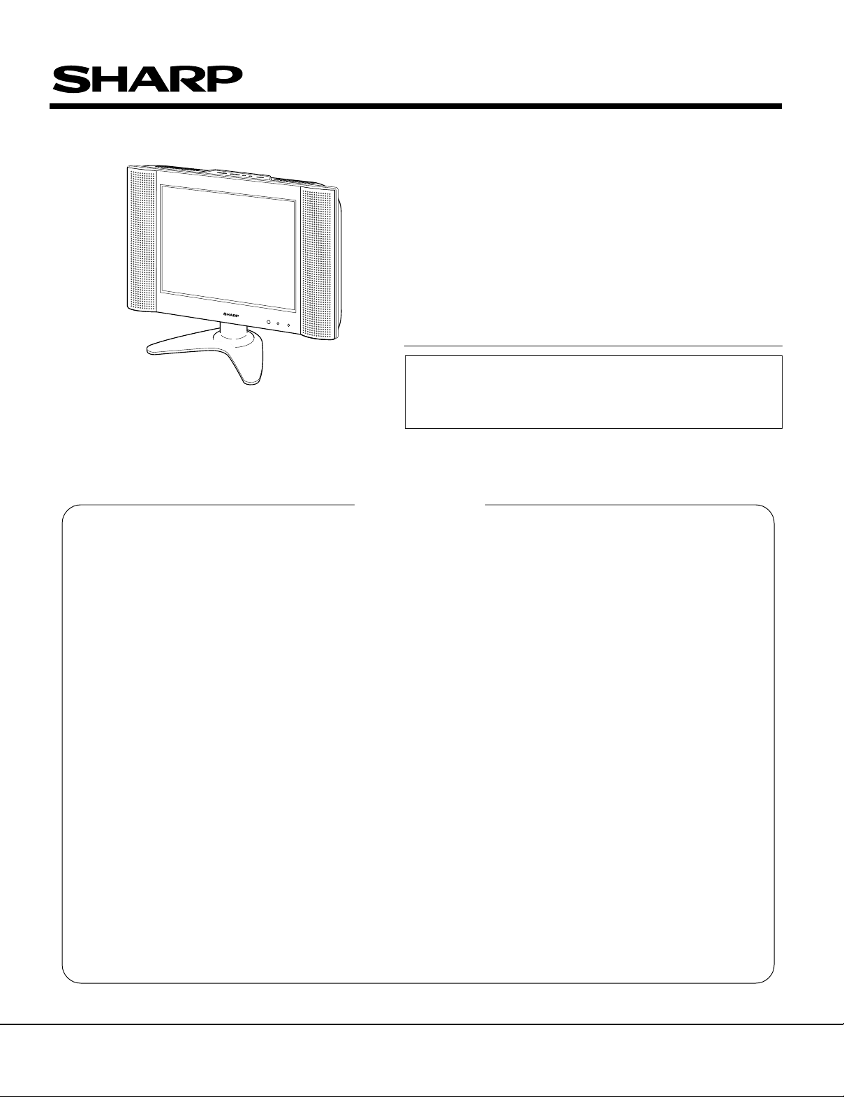
LC-15B1U
CONTENTS
Page
» IMPORTANT SERVICE SAFETY PRECAUTION................................................................................. 2
» PRECAUTIONS FOR USING LEAD - FREE SOLDER ........................................................................ 4
» SPECIFICATIONS ................................................................................................................................ 5
» OPERATION MANUAL ......................................................................................................................... 6
» DIMENSIONS ....................................................................................................................................... 7
» REMOVING OF MAJOR PARTS .......................................................................................................... 8
» ADJUSTING PROCEDURE OF EACH SECTION ............................................................................. 11
» TROUBLE SHOOTING TABLE........................................................................................................... 23
» CHASSIS LAYOUT ............................................................................................................................. 28
» BLOCK DIAGRAMS............................................................................................................................ 30
» DESCRIPTION OF SCHEMATIC DIAGRAM ..................................................................................... 32
» SCHEMATIC DIAGRAMS ................................................................................................................... 33
» PRINTED WIRING BOARD ASSEMBLIES........................................................................................ 47
» PARTS LIST
Ë
ELECTRICAL PARTS..................................................................................................................... 62
MAIN UNIT ..................................................................................................................................... 62
TERMINAL UNIT............................................................................................................................ 66
CONTROL UNIT ............................................................................................................................ 69
LED UNIT ....................................................................................................................................... 69
INVERTER UNIT............................................................................................................................ 69
Ë
CABINET PARTS LIST................................................................................................................... 70
Ë
SUPPLIED ACCESSORIES PARTS .............................................................................................. 70
Ë
PACKING PARTS ........................................................................................................................... 70
Ë
CABINET AND MECHANICAL PARTS.......................................................................................... 71
» PACKING OF THE SET ...................................................................................................................... 73
SHARP CORPORATION
This document has been published to be used for
after sales service only.
The contents are subject to change without notice.
1
Page 2
LC-15B1U
2
2
Ë
Service work should be perfomed only by qualified service technicians who are thoroughly familiar
with all safety checks and the servicing guidelines which follow:
IMPORTANT SERVICE SAFETY PRECAUTION
WARNING
1. For continued safety, no modification of any circuit
should be attempted.
2. Disconnect AC power before servicing.
CAUTION
FOR CONTINUED PROTECTION
AGAINST A RISK OF FIRE REPLACE
ONLY WITH SAME TYPE FUSE.
A V
F3701 (2A, 125V), F6500 (1.6A, 125V), F6501 (1.6A,
125V) FUSE.
BEFORE RETURNING THE RECEIVER
(Fire & Shock Hazard)
Before returning the receiver to the user, perform
the following safety checks:
1. Inspect all lead dress to make certain that leads are
not pinched, and check that hardware is not lodged
between the chassis and other metal parts in the
receiver.
2. Inspect all protective devices such as non-metallic
control knobs, insulation materials, cabinet backs,
adjustment and compartment covers or shields,
isolation resistor-capacitor networks, mechanical
insulators and etc.
3. To be sure that no shock hazard exists, check for
leakage current in the following manner.
• Plug the AC cord directly into a 110~240 volt A C outlet,
and connect the DC power cable into the receiver's
DC jack. (Do not use an isolation transformer for this
test).
• Using two clip leads, connect a 50k ohm, 10 watt resistor
paralleled by a 0.15µF capacitor in series with all
exposed metal cabinet parts and a known earth ground,
such as electrical conduit or electrical ground connected
to an earth ground.
• Use an AC voltmeter ha ving with 5000 ohm per volt, or
higher, sensitivity or measure the AC voltage drop
across the resisor.
• Connect the resistor connection to all exposed metal
parts having a return to the chassis (antenna, metal
cabinet, screw heads, knobs and control shafts,
escutcheon and etc.) and measure the AC voltage drop
across the resistor.
All checks must be repeated with the AC cord plug
connection reversed. (If necessar y, a nonpolarized
adaptor plug must be used only for the purpose of
completing these checks.)
Any reading of 0.75V peak (this corresponds to 0.5
milliamp. peak A C .) or more is e xcessive and indicates
a potential shock hazard which must be corrected
before returning the monitor to the owner .
DVM
AC SCALE
50k ohm
10W
0.15 µF
TEST PROBE
TO EXPOSED
METAL PARTS
CONNECT TO
KNOWN EARTH
GROUND
234567890123456789012345678901212345678901234567890123456789012123456789012345678901234567890121
SAFETY NOTICE
Many electrical and mechanical parts in LCD television
have special safety-related characteristics.
These characteristics are often not evident from visual
inspection, nor can protection afforded by them be
necessarily increased by using replacement components
rated for higher voltage, wattage and etc.
Replacement parts which have these special safety
characteristics are identified in this manual; electrical
and shaded areas in the
Schematic Diagrams
For continued protection, replacement parts must be
identical to those used in the original circuit.
The use of a substitute replacement parts which do not
have the same safety characteristics as the factory
recommended replacement parts shown in this service
manual, may create shock, fire or other hazards.
components having such features are identified b y “ å”
234567890123456789012345678901212345678901234567890123456789012123456789012345678901234567890121
2
Replacement Parts Lists
.
and
Page 3
5
5
PRECAUTIONS A PRENDRE LORS DE LA REPARATION
Ë
Ne peut effectuer la réparation qu’ un tec hnicien spécialisé qui s’est parfaitement accoutumé
à toute vérification de sécurité et aux conseils suivants.
LC-15B1U
AVERTISSEMENT
1. N’entreprendre aucune modification de tout circuit.
C’est dangereux.
2. Débrancher le récepteur avant toute réparation.
PRECAUTION
POUR LA PROTECTION CONTINUE
CONTRE LES RISQUES D’INCENDIE,
REMPLACER LE FUSIBLE PAR UN FUSIBLE
DE MEME TYPE F3701 (2A, 125V), F6500
(1.6A, 125V), F6501 (1.6A, 125V) FUSE.
A V
• Utiliser un voltmètre CA d’une sensibilité d’au moins
5000Ω/V pour mesurer la chute de tension en travers
de la résistance.
• Toucher avec la sonde d’essai les piéces métalliques
exposées qui présentent une v oie de retour au châssis
(antenne, coffret métallique, tête des vis, arbres de
commande et des boutons, écusson, etc.) et mesure
la chute de tension CA en-travers de la résistance.
T outes les vérifications doivent être refaites aprés a voir
inversé la fiche du cordon d’alimentation. (Si
nécessaire, une prise d’adpatation non polarisée peut
être utilisée dans le but de terminer ces vérifications.)
Une valeur de 0.75 V RMS ou plus (correspond à 0.5
VERIFICATIONS CONTRE L’INCEN-DIE ET
LE CHOC ELECTRIQUE
mA C.A.) est excessive et implique un danger de
secousse électrique, qui devra être supprimé avant
de retourner l'appareil à l'utilisateur.
Avant de rendre le récepteur à l’utilisateur, effectuer
les vérifications suivantes.
1. Inspecter tous les faisceaux de câbles pour s’assurer
que les fils ne soient pas pincés ou qu’un outil ne soit
pas placé entre le châssis et les autres pièces
métalliques du récepteur.
2. Inspecter tous les dispositifs de protection comme les
boutons de commande non-métalliques, les isolants,
le dos du coffret, les couvercles ou blindages de
réglage et de compartiment, les réseaux de résistance-
VTVM
ECHELLE CA
50K OHMS
10W
capacité, les isolateurs mécaniques, etc.
3. S’assurer qu’il n’y ait pas de danger d’électrocution en
vérifiant la fuite de courant, de la facon suivante:
• Brancher le cordon d’alimentation dans la prise CA de
110~240 V et le câble d’alimentation CC dans le jack
du moniteur. (Ne pas utiliser un transformateur pour
0.15 µF
SONDE D'ESSAI
cet essai.)
• A l’aide de deux fils à pinces, brancher une résistance
de 1,5kΩ 10 watts en paralléle avec un condensateur
de 0,15µF en série avec toutes les pièces métalliques
exposées du coffret et une terre connue comme une
conduite électrique ou une prise de terre branchée à
VERS PIECES
METALLIQUES
EXPOSEES
CANNECTER A
UNE MASSE DE
TERRE CONNUE
la terre.
234567890123456789012345678901212345678901234567890123456789012123456789012345678901234567890121234
AVIS POUR LA SECURITE
De nombreuses pièces, électriques et mécaniques, dans
les téléviseurs présentent des caractéristiques spéciales
relatives à la sécurité, qui ne sont souvent pas évidentes
à vue. Le degré de protection ne peut pas être
nécessairement augmentée en utilisant des pièces de
remplacement étalonnées pour haute tension, puissance,
etc.
Les pièces de remplacement qui présentent ces
caractéristiques sont identifiées dans ce manuel; les
pièces électriques qui présentent ces particularités sont
234567890123456789012345678901212345678901234567890123456789012123456789012345678901234567890121234
identifiées par la marque “ å” et hachurées dans
des pièces de remplacement et les diagrammes
schématiques.
Pour assurer la protection, ces pièces doivent être
identiques à celles utilisées dans le circuit d’origine.
L’utilisation de pièces qui n’ont pas les mêmes
caractéristiques que les pièces recommandées par l’usine,
indiquées dans ce manuel, peut provoquer des
électrocutions, incendies, radiations X ou autres accidents.
3
la liste
Page 4
LC-15B1U
Ë
Precautions for using lead-free solder
1 Employing lead-free solder
“Main PWB” of this model employs lead-free solder. The LF symbol indicates lead-free solder, and is attached
on the PWBs and service manuals. The alphabetical character following LF shows the type of lead-free solder.
Example:
2 Using lead-free wire solder
When fixing the PWB soldered with the lead-free solder, apply lead-free wire solder. Repairing with conventional
lead wire solder may cause damage or accident due to cracks.
As the melting point of lead-free solder (Sn-Ag-Cu) is higher than the lead wire solder by 40°C, we recommend
you to use a dedicated soldering bit. If you are not familiar with how to obtain lead-free wire solder or soldering bit,
contact our service station or service branch in your area.
Indicates lead-free solder of tin, silver and copper.
3 Soldering
As the melting point of lead-free solder (Sn-Ag-Cu) is about 220°C which is higher than the conventional lead solder
by 40°C, and as it has poor solder wettability, you may be apt to keep the soldering bit in contact with the PWB
for extended period of time. However, since the land may be peeled off or the maximum heat-resistance
temperature of parts may be exceeded, remove the bit from the PWB as soon as you confirm the steady soldering
condition.
Lead-free solder contains more tin, and the end of the soldering bit may be easily corroded. Make sure to turn on
and off the power of the bit as required.
If a different type of solder stays on the tip of the soldering bit, it is alloyed with lead-free solder. Clean the bit after
every use of it.
When the tip of the soldering bit is blackened during use, file it with steel wool or fine sandpaper.
Be careful when replacing parts with polarity indication on the PWB silk.
Special attention must be paid to coils of L6500 - L6503.
Lead-free wire solder for servicing
Part No. ★ Description Code
ZHNDAi123250E J φ 0.3 mm 250 g (1 roll) BL
ZHNDAi126500E J φ 0.6 mm 500 g (1 roll) BK
ZHNDAi12801KE J φ 1.0 mm 1 kg (1 roll) BM
4
Page 5

SPECIFICATIONS
LCD panel................................................ 15" Advanced Super View & Black TFT LCD
Number of dots ..................................................................................921,600 dots VGA
Video color system ..............................N358/N443/PAL/PAL-M/PAL-N/SECAM/PAL-60
TV Function
Destination...................................................................................... USA/Latin A/Twn
TV-Standard (CCIR) ................................................................. NTSC/PAL-M/PAL-N
TV-Tuning System...................................................................................PLL 181 ch.
Stereo .....................................................................................................MTS + SAP
CATV.............................................................................................................. 125 ch.
4-line comb filter ....................................................................................................... Yes
Audio output.....................................................................................................2.1 W x 2
Speakers...............................................................1-37/64 x 2-3/4 in. (4 x 7 cm), 2 pcs.
Terminals
AV1 ........................................................................................... AV-IN1, S-VIDEO-IN
AV2 ...................................................................................................AV-IN2/AV-OUT
Component .................................................................. COMPONENT-IN, AUDIO-IN
Antenna .......................................................................................................... F-Type
Headphone ...................................................................... Mini-jack for stereo (3.5 φ)
PC Card slot ...................................................... PC Card Type ll (PC Card adapter)
Image File Format............................................. JPEG files complying with DCF format
OSD language ..........................................................................English/French/Spanish
Power supply........................................................... DC 12 V, AC 110 - 240 V, 50/60 Hz
Power consumption ............................................................AC 43 W (With AC adapter)
DC 37 W (DC 12 V)
Weight.......................................................................11.7 lbs (5.3 kg), w/o accessories
Accessories ................................................Remote Control, Batteries, Antenna cable,
AC adapter, AC cord, Cable clamp
LC-15B1U
Æ
The LCD display is manufactured with concentrated precision technology, and has
effective pixels of more than 99.99%. 0.01% of them may be missing or all the time.
This is normal.
Specifications are subject to change without prior notice.
5
Page 6
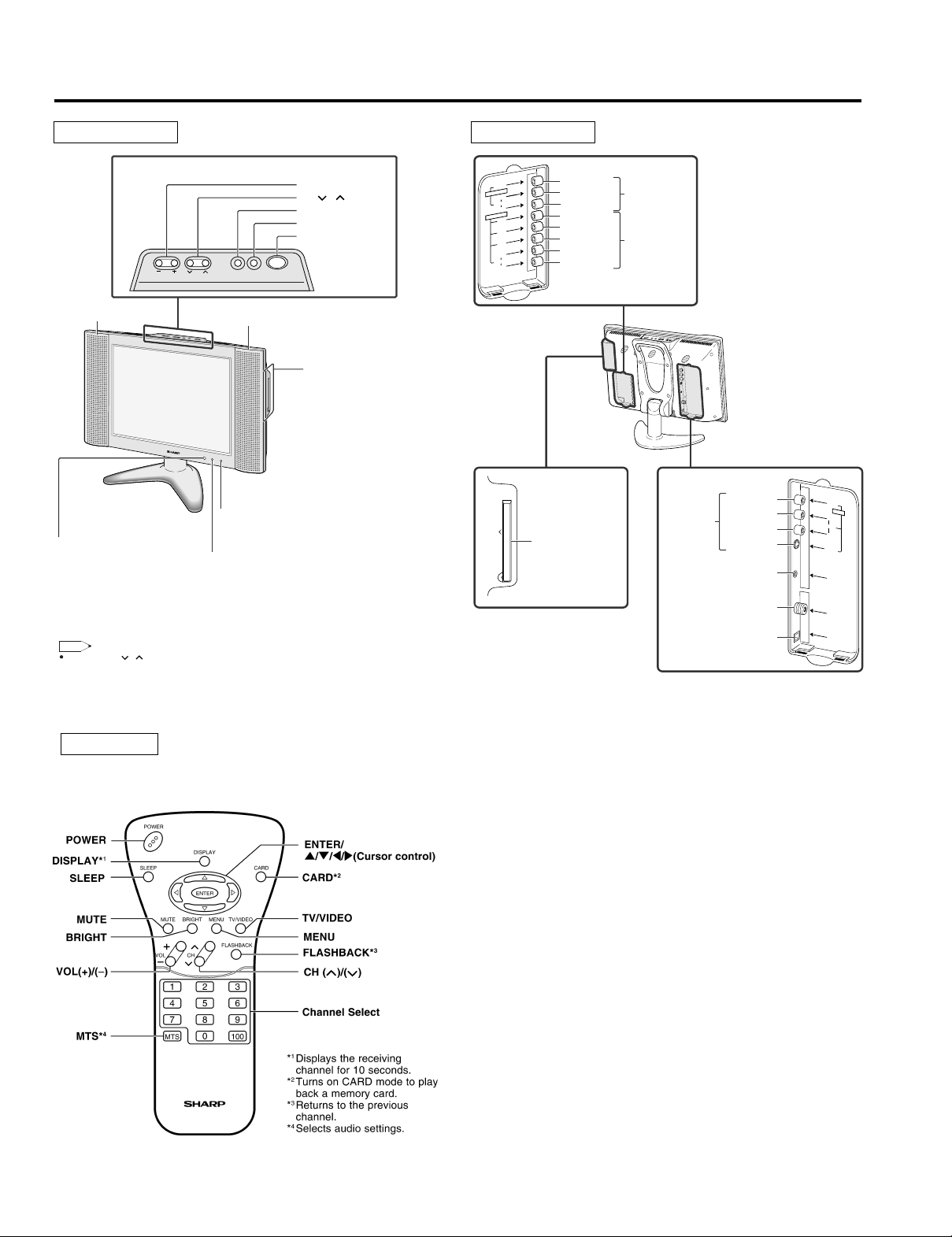
LC-15B1U
PC CardPC Card
OPERATION MANUAL
Main unit (Front view)
Upper control panel
VOL
CH MENU TV/VIDEO MAIN POWER
Speaker
Remote sensor window
Note
TV/VIDEO, CH ( )/( ), VOL (–)/(+), and MENU on the main unit have the same functions as the same buttons
on the remote control. Fundamentally, this operation manual provides a description based on operation with the
remote control.
Speaker
P
O
W
E
R
S
L
E
E
P
SLEEP indicator
The SLEEP indicator lights up red when
the SLEEP TIMER is set to on.
POWER indicator
A green indicator lights when the power is
on and a red indicator lights when in the
standby mode (the indicator will not light
when the main power is off).
VOL (–)/(+)
CH (
)/( )
MENU
TV/VIDEO
MAIN POWER
PC Card slot
To change the vertical angle of the LCD
TV set, tilt the screen up to 5 degrees
forward or 10 degrees backward. The
TV set can also be rotated 50 degrees
horizontally. Please adjust the angle so
that the TV set can be watched most
comfortably.
Main unit (Rear view)
VIDEO
AV-IN2/OUT
AUDIO
COMPONENT
AUDIO
L
R
Y
B
P
R
P
L
R
VIDEO
AUDIO (L)
AUDIO (R)
Y
P
B
R
P
AUDIO (L)
AUDIO (R)
PC Card slot
AV-IN2/OUT
COMPONENT
R
E
W
O
P
N
I
A
M
O
E
D
I
V
/
V
T
U
N
E
CH M
L
O
V
AV-IN1
HEADPHONE
Antenna terminal
POWER INPUT
(DC 12V)
VIDEO
AUDIO (L)
AUDIO (R)
S-VIDEO
V
ID
E
O
A
V
-IN
1
L
A
U
D
IO
R
S
-
V
ID
E
O
H
E
A
D
P
H
O
N
E
A
N
T
.
P
O
W
E
R
IN
P
U
T
D
C
1
2
V
Remote Control
6
Page 7
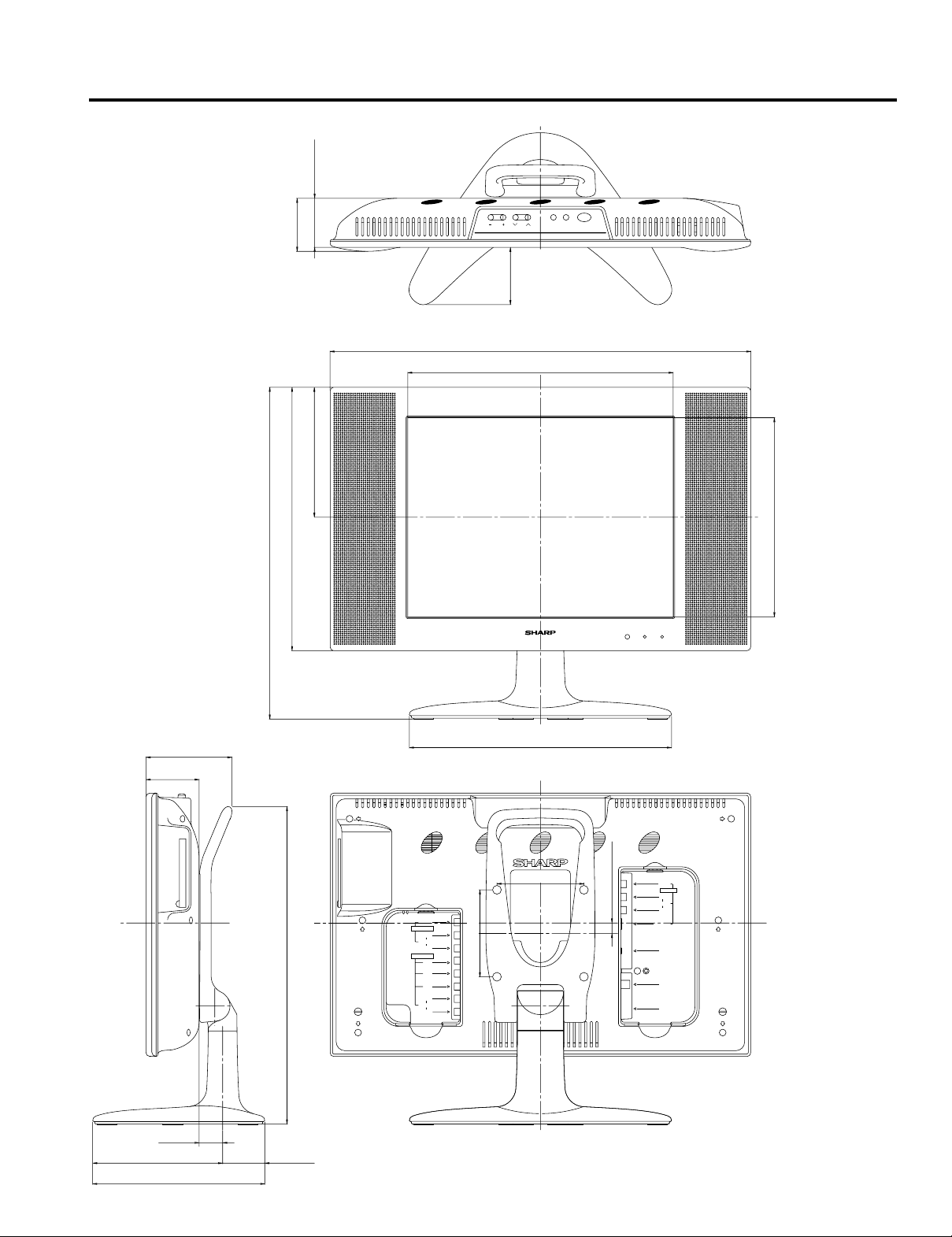
DIMENSIONS
/56.5
7/32
2-
LC-15B1U
/303
59/64
11-
/381.7
1/32
15-
/61.1
13/32
2-
/149.5
57/64
5-
CHVOL TV/VIDEOMENU MAIN POWER
/66
19/32
2-
19-
1/16
/484
1/64
/305.3
12-
/229
1/64
9-
57/64
/98.8
3-
13/32
/61.1
2-
1-
1/16
/27
5-
57/64
/149.5 1-
7-
51/64
/198
/365.2
3/8
14-
29/32
/48.5
VIDEO
AV-IN 2/OUT
AUDIO
COMPONENT
AUDIO
11-
7/8
/301.6
3-
15/16
/100
L
R
Y
P
B
R
P
L
R
/100
15/16
3-
/11.8
15/32
S-VIDEO
VIDEO
AUDIO
L
R
HEAD
PHONE
ANT.
POWER
INPUT
DC12V
AV-IN1
(Unit: Inch/mm)
7
Page 8
LC-15B1U
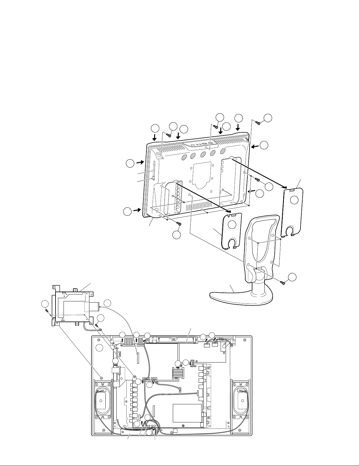
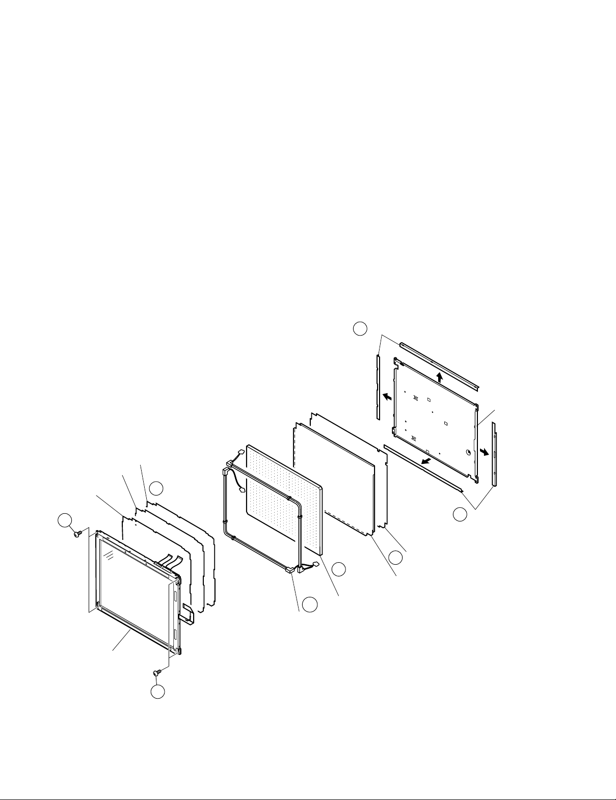
REMOVING OF MAJOR PARTS
1. Remove two Rear covers.
2. Remove the Table stand fixing screws (4 pcs.).
3. Remove the Cabinet B fixing screws (10 pcs.) and detach the cabinet.
4. Push on the hooksof the Cabinet B, open the cabinet and detach eight hooks,
and then detach the Cabinet B.
5. Remove the PC card
5-1. Detach the connector.
5-2. Remove the PC card frame angle
fixing screws (2 pcs).
6. Detach the connector from each PWB.
4
4
3
4
3
4
3
4
4
5-2
PC Card Slot
PC Card Eject button
4
Cabinet B
PC Card Frame Angle
PC Card PWB
[ CAUTION ]
When you attach FFC , a
Black dot mark should be
5-1
on a card unit side
5-2
Rear cover (L)
3
4
1
Rear
cover (S)
1
3
2
Table stand
Control PWB
66
6
6
6
5-2
6
SC1203
LED PWB
SC1202 SC1201
6
P3503
6
P3501
P2003
P3500
6
6
6
Main PWB
P2004
P3601
P4005
6
SC2001
P3702
Terminal PWB
8
Inverter PWB
P6502
6
P3703
SC3403
P3504
P6500
P6501
Page 9
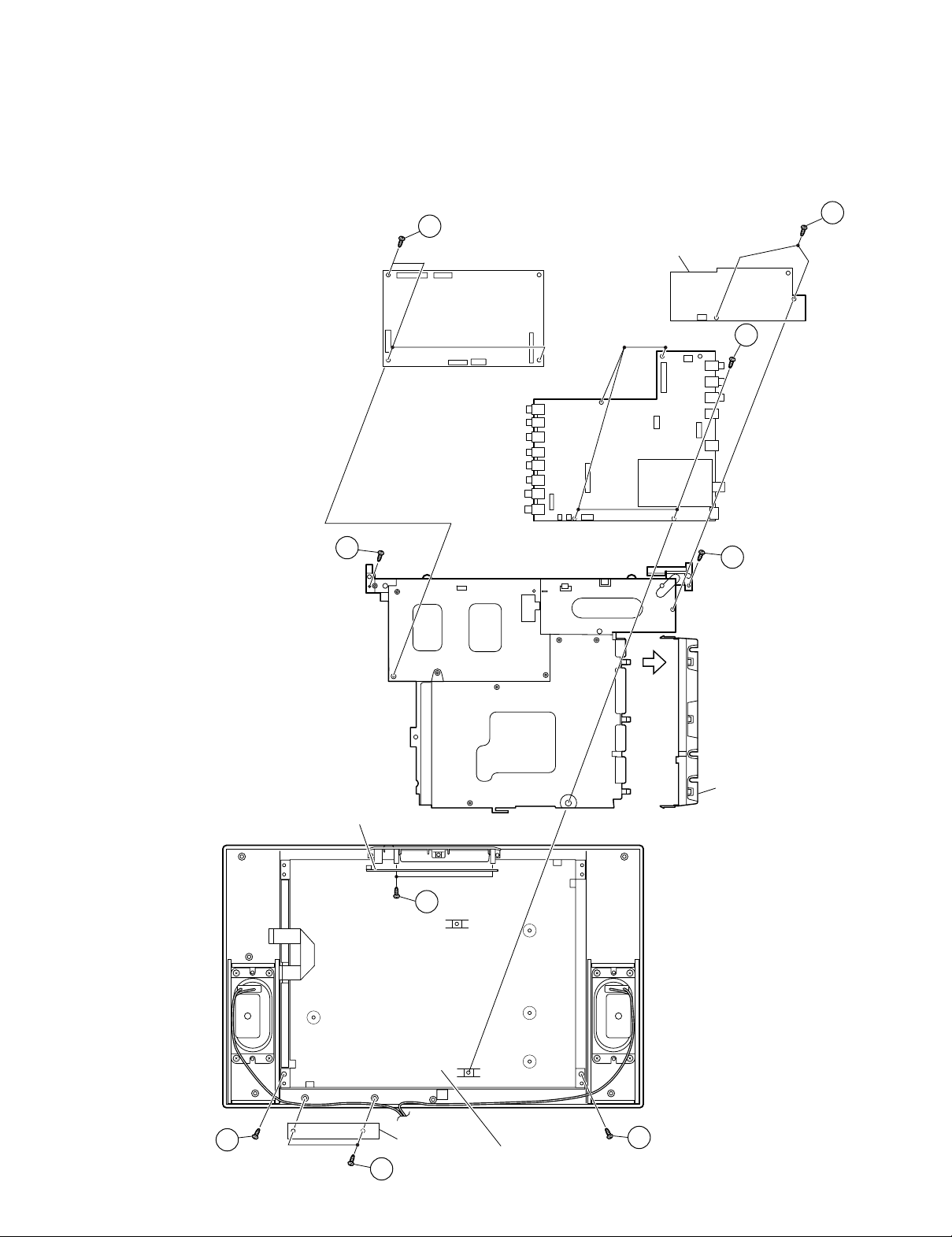
7. Remove the Main PWB fixing screws (3 pcs.).
8. Remove the Inverter PWB fixing screw (2 pcs.).
9. Remove the Terminal PWB fixing screws (4 pcs.).
10. Remove the LED PWB fixing screws (2 pcs.).
11. Remove the Control PWB fixing screws (2 pcs.).
12. Remove the LCD Unit fixing screws (4 pcs.).
LC-15B1U
12
7
8
Inverter PWB
Main PWB
9
Terminal PWB
12
12
Control PWB
10
11
LED PWB
LCD Unit
9
Chassis Frame
12
Page 10
LC-15B1U
13. Remove the LCD display unit fixing screws (4 pcs.).
14. Detach the Reflection/deflection sheet, Pr ism sheet and Diffusion sheet.
15. Detach four Reflection mirrors.
16. Remove the Fluorescent lamp.
17. Detach the Light guide plate.
18. Detach two Lamp reflection sheets.
Prism sheet
(PSHEP0282CEZZ)
Reflection/deflection sheet
(PSHEP0283CEZZ)
14
Diffusion sheet
(PSHEP0281CEZZ)
15
Fluorescent lamp
(KLMP-0122CEZZ)
17
16
Reflection mirror
19
18
Light guide plate
(PGiDM0070CEZZ)
16
Lamp reflection sheet-1
(PSHEP0284CEZZ)
Lamp reflection sheet-2
(PSHEP0285CEZZ)
Shielding plate
(PSLDM4689CEFW)
Reflection mirror
LCD display unit
(RLCDTA003WJZZ)
14
10
Page 11

LC-15B1U
ADJUSTING PROCEDURE OF EACH SECTION
The best adjustment is made before shipping. If any position deviation is found or after part replace is performed, adjust
as follows.
1.Preparation for Adjustments
(1) Use the exclusive-use AC adapter or stable DC power supply.
AC adapter: UADP-0242CEPZ
DC power supply: 12 ± 0.5V
2.Special mode setting procedure
(1) After initialization of E2PROM the mode is changed to the adjustment mode.
[Procedure]
Connect TP2001 and TP2002 to GND, and turn on the power.
[Description]
» The initialization of microcomputer is as follows.
» AV position, DAC data, G/A data, sound processor data, and video chroma data adjustment values are taken as
defaults.
(2) Adjustment mode
[Procedure]
Short-circuit TP2001 to GND, and turn on the power.
Or short-circuit TP2002 to GND, and turn on the power.
Or holding down the [TV/VIDEO] key and [MENU] key, turn on the main power, and simultaneously press the
(inspection process) [CH "] key and [VOL –] key to change the mode to the adjustment mode.
[Description]
The manual adjustment or adjustment through communication with the automatic machine is performed.
(3) Shipping setting mode
[Procedure]
Holding down the [TV/VIDEO] key and [MENU] key, turn on the main power, and simultaneously press the
(inspection process) [CH '] key and [VOL +] key to change the mode to the shipping setting mode.
Note: Keep it in mind to turn off the power immediately. If any key-in is accidentally made, the setting will be
canceled.
[Description]
User adjustment and other values are taken as defaults.
If TV is indicated as SETTING COMPLETE, setting has been completed.
3.Cancel of special mode
Turn off the main unit power.
11
Page 12
LC-15B1U
4.Adjustments
Adjustment Adjusting conditions Adjusting method
1 B+ Adjustment
(R3760)
2 Inch Size setup
(If E2PROM is replaced)
(IC2004)
3 Common-bias
adjustment
4 TAMP adjustment
1. Connect the DC voltmeter to pin (2) of
P3702.
1. Go to the adjustment mode.
1. Receive a B/W channel.
2. Go to the adjustment mode.
3. Select the "COM BIAS" with [MENU]
key.
1. In the TV mode, the unit receives a
picture of the half color bar signal
whose left top corner is 75% white.
The signal does not have to be the
half color bar as long as the 180th
line from the top and 46th pixel from
the left is 75% white. (Data at this
point is used for adjustment.)
1. Adjust the "B+ Adj" value to
5.0 ± 0.02V with R3760.
* Keep the voltage at pin (2) of P3702
below 5.3V during the adjustment.
1. Select "INCH SIZE" and adjust to
"15" with [VOL +] or [VOL –] key.
* The color of "INCH SIZE" must be
yellow.
1. Adjust "COM BIAS" to the darkest
screen with [VOL +] and [VOL –] key.
* The color of "COM BIAS" must be
yellow.
Upper left 75%
Vertical: 180th line
Horizontal: 46th pixel
640 pixels
480 lines
2. Adjust "NTSC TAMP" on the page 2
of the adjustment process mode so
that the "Y" value on the same page
falls between BF - C9.
Page 2 of the adjustment process
mode
2
| COM BIAS 120
NTSC TAMP 27
PAL-M TAMP 27
PAL-N TAMP 27
RCUTOFF 0
GCUTOFF 0
BCUTOFF 0
G3 B3 R3 00 00 00
G1 B4 Y DF DE B5
TAMP H C9
TAMP L BF
GAIBU VER 0.000
Y-Data
(White 100%)
3. Set the values of PAL-M TAMP and
PAL-N TAMP same.
12
Page 13

Adjustment Adjusting conditions Adjusting method
LC-15B1U
5 White balance
adjustment
6 Checking and modifying
the settings
(If E2PROM is replaced)
1. Receive the monoscope pattern
signal.
2. Adjust the "RCUTOFF" and
"BCUTOFF" settings on the page 2
of the adjustment process mode to
become the proper white balance.
Do not change the "GCUTOFF"
settings. (It also change the black
level.)
1. Go to the adjustment mode and
check the following settings.
» V176 137
» V64 73
» V21 50
» V0 BIAS 130
1. See if all the settings are as specified.
If not, select an item in question with
[VOL +] or [VOL –] key and adjust the
setting as shown at left.
* An item selected will be highlighted
in yellow.
13
Page 14
LC-15B1U
5.Shipping setting list
Channel............................................................................................................................................... 2ch
Air/Cable ............................................................................................................................................. Air
Skip Data_CATV................................................................................................................................. All Skip
Skip Data_AIR .................................................................................................................................... All Skip
Volume................................................................................................................................................ 20
Picture................................................................................................................................................. 30
Tint ...................................................................................................................................................... 0
Color ................................................................................................................................................... 0
Black Level ......................................................................................................................................... 0
SHARPNESS...................................................................................................................................... 0
RED-BLUE.......................................................................................................................................... 0
GREEN ............................................................................................................................................... 0
TV Color System................................................................................................................................. N358
AV Color System ................................................................................................................................ Auto
Language............................................................................................................................................ English
Blue Screen ........................................................................................................................................ Off
EZ Setup Auto Start............................................................................................................................ On
Sleep Timer ........................................................................................................................................ None
MTS .................................................................................................................................................... Stereo
Brightness........................................................................................................................................... Bright
Auto Power Off ................................................................................................................................... Off
Upside................................................................................................................................................. Normal
Right/Left ............................................................................................................................................ Normal
AV2 IN/OUT........................................................................................................................................ In
Closed Caption (Mode) ...................................................................................................................... OFF
(Data) ....................................................................................................................... CH1
V Chip block (MPAA) ..................................................................................................................... None
(TV Guideline) .......................................................................................................... None
(Block Content) ........................................................................................................ All Unblock
(Status)..................................................................................................................... Off
(Input Secret No.)..................................................................................................... Clear
CARD
CARD MODE CARD
SLIDE SHOW SETTING INTERVAL 5SEC
ORDER TO SHOW NORMAL
REPEAT OFF
SOUND SETTING TV — — (OFF)
AV1 — — (OFF)
AV2 — — (OFF)
COMPONENT — — (OFF)
14
Page 15
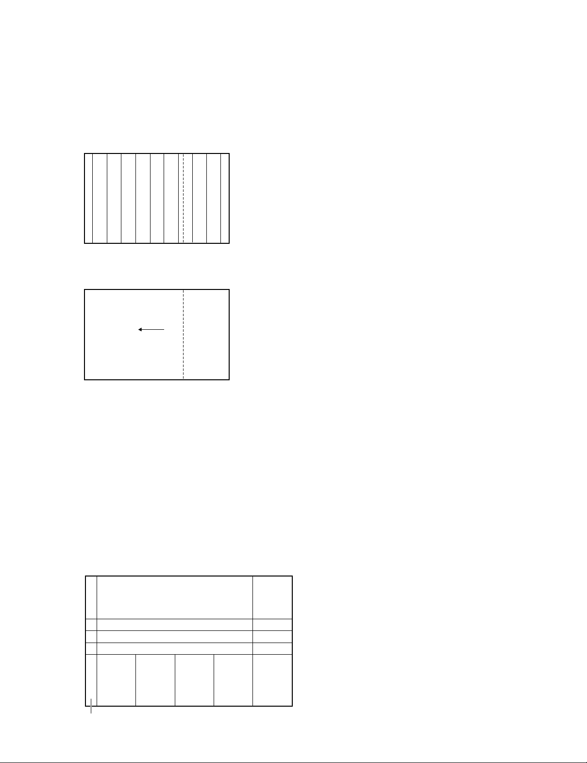
6.Test patterns in adjustment process mode
(1) IC801 (video decoder) test pattern
1-1) Indication of the test pattern
Set the screen to AV1, AV2, or component, and do not input a signal.
It enters the adjustment process mode. By selecting “TEST PATTERN” on the third line of page 7 and changing
the setting value to one of 1 - 6, the test pattern will be displayed.
1-2) Description of test pattern
• In Setting 1
The color bar as shown to the left will appear.
LC-15B1U
Green
Yellow
Cyan
Magenta
Green
Red
Blue
Green
Yellow
Cyan
Magenta
• In Setting 2
A striped pattern with narrower bars than in Setting 1 will appear.
• In Setting 3
Green
Bright Bright
Dark
Green pattern as shown to the left will appear.
• In Setting 4
Green pattern of slightly dark tone will appear.
• In Setting 5
Green pattern of middle tone will appear.
• In Setting 6
Green pattern of slightly bright tone will appear.
(2) Test pattern of IC1201 (LCD controller)
2-1) How to display the test pattern
Set the screen to AV1, AV2, or component, and do not input a signal.
It enters the adjustment process mode. By selecting “G/A TEST PATTERN” on the 13th line of page 16 and
changing the setting value to ON, the test pattern will be displayed.
2-2) Description of the test pattern
The test pattern as shown to the below will appear.
(Bright)
(Bright)
(Bright)
(Bright)
Grey
(48 grey level)
(Dark)
(Dark)
(Dark)
(Dark)
White
(63 grey level)
White
(Dark)
(Dark)
(Dark)
(Dark)
White
(0 grey level)
Grey scale
Red
Green
Blue
Grey
(16 grey level)
Grey
(32 grey level)
Note: If both test pattern displays of IC801 and IC1201 are set to ON, that of IC1201 will prevail.
15
Page 16
LC-15B1U
(3) Trouble shooting using test patterns
Is the test pattern of IC801
displayed normally?
Is the test pattern of IC1201
displayed normally?
Check the signal output
line of IC801, IC801 and
its peripheral circuits.
Is the waveform of signal
input pins of IC801 normal?
TV/Composite.......Pin (73)
S-video........Pins (71), (72)
Component.....Pins (4), (5),
(6), (75)
Check IC801 and its
peripheral circuits.
Check IC1201 and its
peripheral circuits, voltage of
LCD panel and waveform.
Check the signal input line
of IC801.
Is the waveform of pins
(10), (11), (13), (15), (17)
of IC1201 normal?
Check the line, IC801 and its
peripheral circuits.
16
Page 17
Descriptions of the terminals of Micon IC (IC2001) RH-iXA276WJZZQ
LC-15B1U
No. Terminal Name Descriptions
1 V HOLD For closed caption
2 HLF For closed caption
3 MAINSW Main switch ON “H” / OFF “L”
4 TIMELED For LED lighting when off-timer is ON
5 M/S OUT Master-slave output for sub-micon
6 CSYNC Composite synchronized signal
7 IREMI Remote control
8 GND GND grounding
9 GND GND grounding
10 XCIN 32 kHz oscillation input
11 XOUT 32 kHz oscillation output
12 RESET Reset state in “L”
13 XOUT Oscillator connection in micon part
14 GND GND grounding
15 XIN Oscillator connection in micon part
16 VCC Power source
17 OSCIN Clock input for OSD
18 OSCOUT Clock output for OSD
19 PSWIN Main power source input
20 SUBREADY READY input for sub-micon
21 BLK Blanking output for OSD
22
23 DAC1CS DAC1 chip select
24 DAC2CS DAC2 chip select
25 DSW Detection for D-terminal connection
26 DTV Control line for D-terminal
27 MRDY Input for I2C bus open-connection change
28 SCL2 I2C bus serial clock line 2
29 SCL1 I2C bus serial clock line 1
30 SDA1 I2C bus serial data line 1
31 SDA2 I2C bus serial data line 2
32 R R-signal output
33 G G-signal output
34 B B-signal output
35 SUBDOUT Data output for sub-micon
36 SUBDIN Data input for sub-micon
37 SUBCLK Clock input for sub-micon
38
39 MRDY OUT I2C open-connection output
40 FCH
41 IREM OUT Not used
42 L_ERR Fluorescent lamp error detection input
43 S IN/OUT AUDIO IN/OUT change
44 N443 “H” in N443, “L” in others
45 PAL “H” in PAL, “L” in others
46 SECAM “H” in SECAM, “L” in others
47 PAL_M “H” in PAL-M, “L” in others
48 N358 “H” in N358, “L” in others
49 PXOE Card (Card mode in “L”)
50 VSH OUT Control for panel gate driver voltage
Field-destinctional signal output when no signals
No. Terminal Name Descriptions
51 REQ Adjusting procedure
52 AV/SY/DY2 CCD input change for US
53 FSMUTE Front speaker mute
54 RSMUTE Rear speaker mute
55 HPDET Headphones detection: detect in “L”
56 SSTBY Speaker standby (“H” in standby state)
57 VSH IN Check for panel gate driver voltage
58 LMUTE LINE OUT sounds MUTE
59 V IN/OUT VIDEO IN/OUT change
60 SRESET Sound multiplex reset: reset in “L”
61 DENKA
62 VCC Power source
63 CARDPOW Card (ON/OFF)
64 VSS GND grounding
65 TV/AV1 Analog SW 1
66 AV/AV2 Analog SW 2
67 VIS/3DS Analog SW 3
68 AV1/VISY Analog SW 4
69 AV/SY/DY1 CCD input change for US 2
70 STD Micon power-OFF output
71 PMUTE P-mute
72 POWOUT DC/DC control output
73 AD POW Adapter ON/OFF input
74 IREM 2 Receiving in slave state
75 MPRCS G/A read enable
76 MPRDA G/A data input
77 MPCS G/A chip select
78 MPDA G/A data out
79 MPCLK G/A clock
80 DDCRESET Digital decoder reset
81 KEY4 Key input 4
82 KEY5 Key input 5
83 CARDRESET CARD RESET (reset in “H”)
84 SAW SW For the tuner change (use “H”)
85 MODE1 For the tuner change (use “H”)
86 MODE2 For the tuner change (use “H”)
87 SSYSTEM For the detection of S-system change
88 SSW
89 AFT AFT voltage input
90 AGC AGC voltage input
91 KEY1 Key input 1
92 KEY2 Key input 2
93 KEY3 Key input 3
94 POWIN Detection for DC/DC starting
95 VSYNC Vertical sychronized signal for OSD
96 AVSS Analog power input (GND)
97 HSYNC Horizontal sychronized signal for OSD
98 TVSETB For closed caption (GND)
99 AVCC OSD power input
100 CVIN Signal input for closed caption
For counter-measures to the electric charge
S-terminal connection input (S-terminal connection in “L”)
17
Page 18
LC-15B1U
List of the adjustment process mode menu
Page Items
Standard settings
1 INCH SIZE 15 Inch size select Adjustment
MODEL B1U Model name
CARD ON Card system ON/OFF setup
SYSTEM AUTO Color system change
NTSC PWM FREQ OCO Light control frequency setup
PAL PWM FREQ OBD Light control frequency setup
NTSC PWM DUTY 0 Light control duty setup
PAL PWM DUTY 0 Light control duty setup
TV GAIN OFF Auto gain setup in TV mode
ERROR NO RESET 0 Lamp error count and reset Number of times of lamp error
V-CHIP 1 VCHIP line mute setup
CANADIAN VCHIP OFF
Video adjustment
2 COM BIAS 120 Common bias adjustment Adjustment
NTSC TAMP 27 TAMP adjustment Adjustment
PAL-M TAMP 27 TAMP adjustment
P AL-N TAMP 27 T AMP adjustment
RCUTOFF -1 Red cutoff adjustment Adjustment
GCUTOFF 0 Green cutoff adjustment
BCUTOFF -1 Blue cutoff adjustment Adjustment
G3 00 DATA READ Value
B3 00 DATA READ Value
R3 00 DATA READ Value
G1 00 DATA READ Value
B4 00 DATA READ Value
Y 00 DATA READ Value in TAMP adjustment
TAMP H C9 Y max. value setup in TAMP adjustment
TAMP L BF Y min. value setup in TAMP adjustment
3 TV NTSC CONT 50 Video contrast setup (TV NTSC)
TV PAL-M CONT 50 Video contrast setup (TV PAL-M)
TV PAL-N CONT 50 Video contrast setup (TV PAL-N)
AV N358 CONTRAST 50
AV PAL CONTRAST 50
AV SECAM CONTRAST 50
AV PAL-M CONTRAST 50
AV PAL-N CONTRAST 50
AV PAL60 CONTRAST 50
G3 00 DATA READ Value
B3 00 DATA READ Value
R3 00 DATA READ Value
G1 00 DATA READ Value
B4 00 DATA READ Value
Y 00 DATA READ Value
Audio adjustment
4 TV GEQ BAND1 +2.0 Equallizer setup1 (TV)
TV GEQ BAND2 +0.5 Equallizer setup2 (TV)
TV GEQ BAND3 -2.0 Equallizer setup3 (TV)
TV GEQ BAND4 -1.5 Equallizer setup4 (TV)
TV GEQ BAND5 -1.5 Equallizer setup5 (TV)
EXT GEQ BAND1 +2.0 Equallizer setup1 (External input)
EXT GEQ BAND2 +0.5 Equallizer setup2 (External input)
EXT GEQ BAND3 -2.0 Equallizer setup3 (External input)
EXT GEQ BAND4 -1.5 Equallizer setup4 (External input)
EXT GEQ BAND5 -1.5 Equallizer setup5 (External input)
AV C OFF AVC setup
CARRIER MUTE ON
IGR THR 12D IGR THRESH LEVEL
Audio adjustment
5 MSP DATA 0 Audio IC MSP DATA WRITE and READ
MSP DATA WAIT WRITE and READ execute
PRESCALE FM/AM-M 17 Prescale setup (TV)
PRESCALE SCART 15 Prescale setup (External input)
FSP TEST OFF For audio test (FSMUTE ON/OFF)
Video adjustment (VPC setup)
6I2C DATA 0
I2C DATA WAIT WRITE and READ execute
CBW 1 CHROMA band pass setup
NOSEL 3 Comb filter setup
DDR 0 Comb filter setup
Initial settings
Descriptions
CANADIAN VCHIP correspondence setup
Video contrast setup (Composite, S-video)
Video contrast setup (Composite, S-video)
Video contrast setup (Composite, S-video)
Video contrast setup (Composite, S-video)
Video contrast setup (Composite, S-video)
Video contrast setup (Composite, S-video)
Audio output setup in TV mode (no synchronization)
I2C BUS control IC DATA WRITE and READ
Adjustments or descriptions of change
Adjustment (Same value to NTSC TAMP)
Adjustment (Same value to NTSC TAMP)
18
Page 19
LC-15B1U
Page Items
Video adjustment (VPC setup) [Continued]
6 HDG 2 Comb filter setup
VDG 1 Comb filter setup
VPK 3 Comb filter setup
KILVL 08 08 Color killer level setup
KILHY 05 05 Color killer hysterysis setup
VSYNC DELAY 29 V-synchronized phase setup
DVCO -720 DVCO setup
AUTO LCK 1 Line lock mode setup
Video adjustment (Component)
7 VPC DATA 0 Video IC VPC DATA WRITE and READ
VPC DATA WAIT WRITE and READ execute
TEST PATTERN 0 VPC test pattern select Video IC test pattern
AUTO LDLY -2 Y/C phase setup
DVD NTSC CR 25 Color thickness setup (Component)
DVD NTSC CB 28 Color thickness setup (Component)
DVD NTSC TINT +7 Tint setup (Component)
DVD NTSC BRIGHTNESS +64 Brightness setup (Component)
DVD NTSC CONTRAST 28 Contrast setup (Component)
DVD NTSC P FILTER 0 Peaking filter setup (Component)
DVD NTSC H-PEAKING 3 H-peaking setup (Component)
DVD NTSC BRIGHT2 +8 Brightness setup2 (Component)
DVD NTSC CONTRAST2 48 Contrast setup2 (Component)
8 DVD PAL CR 31 Color thickness setup (Component)
DVD PAL CB 31 Color thickness setup (Component)
DVD PAL TINT 0 Tint setup (Component)
DVD PAL BRIGHTNESS +64 Brightness setup (Component)
DVD PAL CONTRAST 27 Contrast setup (Component)
DVD PAL P FILTER 0 Peaking filter setup (Component)
DVD PAL H-PEAKING 3 H-peaking setup (Component)
DVD PAL BRIGHT2 +9 Brightness setup2 (Component)
DVD PAL CONTRAST2 48 Contrast setup2 (Component)
Video adjustment (TV · Composite · S-video)
9 N358 TV COLOR 2600 Color thickness setup (TV)
N358 AV COLOR 2600
N358 TV TINT +70 Tint setup (TV)
N358 AV COLOR +70 Tint setup (Composite, S-video)
N358 BRIGHTNESS +8
N358 PEAKING FILTER 0
N358 TV H-PEAKING 3 H-peaking setup (TV)
N358 AV H-PEAKING 3 H-peaking setup (Composite, S-video)
N358 AVO START 152 Horizontal position setup
N358 SFIF 0 Horizontal position setup
N358 SCINC1 1623 Setup of the degree of true circle
N358 TV LDLY -2 Y/C phase setup (TV)
N358 AV LDLY -2 Y/C phase setup (Composite, S-video)
10 N443 AV COLOR 2600
N443 AV TINT +70 Tint setup (
N443 BRIGHTNESS +8
N443 PEAKING FILTER 0
N443 AV H-PEAKING 3 H-peaking setup (Composite, S-video)
N443 AVO START 152 Horizontal position setup
N443 SFIF 0 Horizontal position setup
N443 SCINC1 1623 Setup of the degree of true circle
N443 AV LDLY -2 Y/C phase setup (Composite, S-video)
11 PAL AV COLOR 2600
PAL AV TINT +70 Tint setup (
PAL BRIGHTNESS +8
PAL PEAKING FILTER 0
PAL AV H-PEAKING 3 H-peaking setup (Composite, S-video)
PAL AVO START 152 Horizontal position setup
PAL SFIF 0 Horizontal position setup
PAL SCINC1 1623 Setup of the degree of true circle
PAL AV LDLY -2 Y/C phase setup (Composite, S-video)
12 SECAM AV COLOR 2600
SECAM AV TINT +70 Tint setup (
SECAM BRIGHTNESS +8
SECAM PEAKING FILTER 0
SECAM AV H-PEAKING 3 H-peaking setup (Composite, S-video)
SECAM AVO START 152 Horizontal position setup
SECAM SFIF 0 Horizontal position setup
SECAM SCINC1 1623 Setup of the degree of true circle
SECAM AV LDLY -2 Y/C phase setup (Composite, S-video)
Initial settings
Descriptions
Color thickness setup (Composite, S-video)
Brightness setup (TV, Composite, S-video)
Peaking filter setup (TV, Composite, S-video)
Color thickness setup (Composite, S-video)
Brightness setup (TV, Composite, S-video)
Peaking filter setup (TV, Composite, S-video)
Color thickness setup (Composite, S-video)
Brightness setup (TV, Composite, S-video)
Peaking filter setup (TV, Composite, S-video)
Color thickness setup (Composite, S-video)
Brightness setup (TV, Composite, S-video)
Peaking filter setup (TV, Composite, S-video)
Composite, S-video
Composite, S-video
Composite, S-video
)
)
)
Adjustments or descriptions of change
19
Page 20

LC-15B1U
Page Items
Video adjustment (TV · Composite · S-video) [Continued]
13 PAL-M TV COLOR 2600 Color thickness setup (TV)
PAL-M AV COLOR 2600
PAL-M TV TINT +70 Tint setup (TV)
PAL-M AV TINT +70 Tint setup (
PAL-M BRIGHTNESS +8
PALM PEAKING FILTER 0
PALM TV H-PEAKING 3 H-peaking setup (TV)
PALM AV H-PEAKING 3 H-peaking setup (Composite, S-video)
PAL-M AVO START 152 Horizontal position setup
PAL-M SFIF 0 Horizontal position setup
PAL-M SCINC1 1623 Setup of the degree of true circle
PAL-M TV LDLY -2 Y/C phase setup (TV)
PAL-M AV LDLY -2 Y/C phase setup (Composite, S-video)
14 PAL-N TV COLOR 2600 Color thickness setup (TV)
PAL-N AV COLOR 2600
PAL-N TV TINT +70 Tint setup (TV)
PAL-N AV TINT +70 Tint setup (Composite, S-video)
PAL-N BRIGHTNESS +8
PALN PEAKING FILTER 0
PALN TV H-PEAKING 3 H-peaking setup (TV)
PALN AV H-PEAKING 3 H-peaking setup (Composite, S-video)
PAL-N AVO START 152 Horizontal position setup
PAL-N SFIF 0 Horizontal position setup
PAL-N SCINC1 1623 Setup of the degree of true circle
PAL-N TV LDLY -2 Y/C phase setup (TV)
PAL-N AV LDLY -2 Y/C phase setup (Composite, S-video)
15 PAL60 AV COLOR 2600
PAL60 AV TINT +70 Tint setup (
PAL60 BRIGHTNESS +8
PAL60 PEAKING FILTER 0
PAL60 AV H-PEAKING 3 H-peaking setup (Composite, S-video)
PAL60 AVO START 152 Horizontal position setup
PAL60 SFIF 0 Horizontal position setup
PAL60 SCINC1 1623 Setup of the degree of true circle
PAL60 AV LDLY -2 Y/C phase setup (Composite, S-video)
AFT reference value setup in search mode / LCD controller setup (NTSC)
16 AFT UP 2.7 AFT voltage reference value
AFT DOWN 1.8 AFT voltage reference value
NTSC 01 8C Initial setting
NTSC 02 C0 Various setting
NTSC 03 81 RCUTOFF
NTSC 04 00 GCUTOFF
NTSC 05 81 BCUTOFF
NTSC 06 0B Horizontal display position
NTSC 07 10 Vertical display position
NTSC 08 00 UV data phase delay
NTSC 09 4C Panel clock adjustment
NTSC 0A 4B
NTSC 10 80 Test pattern display
NTSC 11 00
NTSC 12 00 Horizontal display mask position (left)
NTSC 13 00 Horizontal display mask position (right)
NTSC E0 00 FIFO TEST
NTSC E1 03 Reverse of sinchronized polarity
NTSC F0 07 OFL terminal action setup
NTSC F1 00 Inverter frequency setup
NTSC F2 00 Inverter duty setup
NTSC F3 C0 Light control frequency setup lower level
NTSC F4 00 Light control frequency setup upper level
NTSC F5 00 Light control PWM setup lower level
NTSC F6 00 Light control PWM setup upper level
NTSC F7 00 Phase of OFL1/2
NTSC 14 02 System clock setup
G/A TEST PATTERN OFF Grey level test pattern display LCD controller IC test pattern
LCD controller setup (PAL) / Closed caption setup
17 PAL 01 8E Initial setting
PAL 02 C8 Various setting
PAL 03 81 RCUTOFF
PAL 04 00 GCUTOFF
PAL 05 81 BCUTOFF
Initial settings
Descriptions
Color thickness setup (Composite, S-video)
Brightness setup (TV, Composite, S-video)
Composite, S-video
Peaking filter setup (TV, Composite, S-video)
Color thickness setup (Composite, S-video)
Brightness setup (TV, Composite, S-video)
Peaking filter setup (TV, Composite, S-video)
Color thickness setup (Composite, S-video)
Composite, S-video
Brightness setup (TV, Composite, S-video)
Peaking filter setup (TV, Composite, S-video)
Upper and lower mask position of display screen
Test pattern data
)
)
Adjustments or descriptions of change
20
Page 21

LC-15B1U
Page Items
LCD controller setup (PAL) / Closed caption setup [continued]
17 PAL 06 13 Horizontal display position
PAL 07 18 Vertical display position
PAL 08 O2 UV data phase delay
PAL 09 4C Panel clock adjustment
PAL 0A 4A
PAL 10 80 Test pattern display
PAL 11 00 Test pattern data
PAL 12 00 Horizontal display mask position (left)
PAL 13 00 Horizontal display mask position (right)
PAL E0 00 FIFO TEST
PAL E1 03 Reverse of sinchronized polarity
PAL F0 07 OFL terminal action setup
PAL F1 00 Inverter frequency setup
PAL F2 00 Inverter duty setup
PAL F3 BD Light control frequency setup lower level
PAL F4 00 Light control frequency setup upper level
PAL F5 00 Light control PWM setup lower level
PAL F6 00 Light control PWM setup upper level
PAL F7 00 Phase of OFL1/2
PAL 14 02 System clock setup
CLOSED CAPTION 15 CLOSED CAPTION THRESH LEVEL
CCD ISO 16 CLOSED CAPTION phase setup
AIR SERCH 1.600
Grey level · COM setup
18 V255 255
V255 BIAS 127
V235 226
V235 BIAS 127
V176 137
V176 BIAS 150
V112 103
V112 BIAS 170
V64 73
V64 BIAS 40
V32 62
V32 BIAS 45
19 V21 50
V21 BIAS 50
V17 45
V17 BIAS 55
V7 29
V7 BIAS 65
V0 0
V0 BIAS 130
VGL ADJ 27 VGL bias setup
VGL COM 215 VGL COM setup
COM 181 COM amplitude setup
G/A READDATA 00 00 Controller READ DATA setup
G/A READDATA WAIT READ execute
3-dimension setup / Synchronization judgment setup
20 3D Y/C 0
3D Y/C DA TA 0
3D Y/C DA TA WAIT
LSYNC 625
HSYNC 655
AVSYNC 5000
VPC FP20H
VPC FP21H
VPC FP13H
MSP DEMO200H
L ERROR WAIT 15s
L ERROR H TIME 1.0s
VPC I2C 20H 24
Initial settings
Data 0000
Data 0000
Data 0000
Data 0000
Descriptions
Upper and lower mask position of display screen
Judging frequency of last synchronization in
AIR CH SEARCH mode
Grey level power source reference voltage
Grey level power source reference voltage
Grey level power source reference voltage
Grey level power source reference voltage
Grey level power source reference voltage
Grey level power source reference voltage
Grey level power source reference voltage
Grey level power source reference voltage
Grey level power source reference voltage
Grey level power source reference voltage
Grey level power source reference voltage
Grey level power source reference voltage
Grey level power source reference voltage
Grey level power source reference voltage
Grey level power source reference voltage
Grey level power source reference voltage
Grey level power source reference voltage
Grey level power source reference voltage
Grey level power source reference voltage
Grey level power source reference voltage
3-dimension ON/OFF setup
3-dimension Y/C data WRITE and READ
WRITE and READ execute
Limit value of sychronization judgment (TV)
Limit value of sychronization judgment (TV)
Limit value of sychronization judgment
(External input)
VPC data READ value
VPC data READ value
VPC data READ value
MSP data READ value
Lamp error detection WAIT time
Lamp error detection time
Synchronization control setup
Adjustments or descriptions of change
21
Page 22

LC-15B1U
Page Items
Power off mode / V jitter correspondence / Card setting
21 DENKA PORT OFF Mode setup in power-off time
DENKA TESTP 00 Mode setup in power-off time
DENKA TESTP2 30ms Mode setup in power-off time
CARD FLASH WAIT
RETRY 1 Card data transmission count setting
REMOCON CODE
Card mode LCD controller setting
22 VCP SYNC
OSD
Card 01 8C Initial setting
Card 02 C4 Various setting
Card 03 81 RCUTOFF
Card 04 00 GCUTOFF
Card 05 81 BCUTOFF
Card 06 0B Horizontal display position
Card 07 14 Vertical display position
Card 08 00 UV data phase delay
Card 09 4C Panel clock adjustment
Card 0A 4B Display screen top/bottom mask position
Card 10 80 Test pattern display
Card 11 00 Test pattern data
Card 12 00 Horizontal display mask (left) position
Card 13 00 Horizontal display mask (light) position
Card E0 00 FIFO TEST
Card E1 03 Sync. polarity reversal
Card F0 07 OFL terminal operation setting
Card F1 00 Inverter frequency setting, lower level
Card F2 00 Inverter duty setting
Card F3 C0 Dimmer frequency setting, lower level
Card F4 00 Dimmer frequency setting, upper level
Card F5 00 Dimmer PWM setting, lower level
Card F6 00 Dimmer PWM setting, upper level
Card F7 00 OFL 1/2 phase
Card 14 03 System clock setting
Initial settings
0D8
-30
Descriptions
Card mode sync setting
Card mode OSD position setting
Adjustments or descriptions of change
22
Page 23

TROUBLE SHOOTING TABLE
No Power (Power LED indicator still in red)
Go to the adjustment process mode.
1
INCH SIZE 15
MODEL B1U
CARD ON
SYSTEM AUTO
NTSC PWM FREQ OCO
PAL PWM FREQ OBD
NTSC PWM DUTY 0
PAL PWM DUTY 0
TV GAIN OFF
ERROR NO RESET 5
V-CHIP 1
CANADIAN VCHIP OFF
B2UA VER 1.xx
LC-15B1U
Move the cursor to ERROR NO RESET
and click on it (to reset to zero).
Turn off the power.
Is the power turned on again?
No
Check the following items:
1 Back light lamp
2 Inverter Circuit
(Inverter PWB and Main PWB)
F6500, F6501, D6500, Q6500, Q6501, Q6502,
Q6503, Q6504, Q6505 and their peripheral parts
as well as pin (34) of IC1201.
3 Lamp error detection circuit
(Terminal PWB and Main PWB)
D3600, D3601, D3604, D3605, Q3600, Q3601 and
their peripheral parts as well as pin (42) of IC2001.
Note:
This model is equipped with the lamp error detection function
that detects the current flowing into the fluorescent lamp and
protects the backlight lamp drive circuit.
If a lamp error is detected, the microprocessor interrupts the
unit and the ERROR NO RESET setting will go up.
When the ERROR NO RESET setting has reached "5", the
microprocessor turns and keeps off the unit's power. To
resume the power, take the above procedure to clear the
ERROR NO RESET setting.
23
Page 24

LC-15B1U
No picture
at all
No
Are inputs
and outputs
of IC801 as
specified?
Check all the settings on the microprocessor’s adjust process menu.
No picture
Check IC402
and its
peripheral
parts.
No TV
output
Yes
No
Are voltages
at Pins (6),
(7) and (9) of
tuner as
specified?
Check the
power line.
Yes
No
Is output at
Pin (19) of
tuner as
specified?
Check the
tuner and its
peripheral
parts.
No
Is input at Pin
(3) of IC402
as specified?
Check the
line in
question.
Yes
Check IC402
and its
peripheral
parts.
Yes
No
Are Pins (2)
and (4) of
IC402 at “H”
and “L”
respectively?
Are Pins (65)
and (66) of
IC2001 at “H”
and “L”
respectively?
No S
VIDEO
output
No
Are inputs at
Pins (71) and
(72) of IC801
as specified?
Check
SC3405, SY
line, SC line
and peripheral
parts.
No
COMPONENT
output
No
Is input at
Pins (4), (5),
(6) and (75)
of IC801 as
specified?
Check J3404,
DVD-Y line,
PB line, PR
line and
peripheral
parts.
Yes
Check the
line in
question.
No VIDEO
1 or 2
output
Yes
No
Are inputs
and outputs
of IC402 as
specified?
Check IC402
and its
peripheral
parts.
No
Is input at Pin
(73) of IC801
as specified?
Check IC801,
AV1 line and
their
peripheral
parts.
Yes
Check Pin (88)
of IC2001, or
check SSW
line.
Yes
Yes
No
Is the test-
pattern of
LCD
controller
displayed?
Check
IC1201, its
peripheral
parts and
LCD panel.
No
Check IC801
and its
peripheral
parts.
Is the test-
pattern of
video
decoder
displayed?
TROUBLE SHOOTING TABLE (Continued)
24
Page 25

TROUBLE SHOOTING TABLE (Continued)
No picture and sound
No color
No TV color
No S-VIDEO color
Yes
No
Do F3701 function?
Check all the settings on the microprocessor’s adjust process menu.
No
Are secondary outputs
(+38V, +9V, +5V, -8V, -20V)
of T3701 as specified?
Yes
Are the oscillation waveform
at T3701’s primary side as
specified?
Yes
No
Disconnect F3701.
Is the load side short-
circuited?
Yes
No
Is any of T3701’s primary
side, Q3700 and S4701 short-
circuited?
Check J3701, its peripheral
parts and connection cable.
Replace F3701.
Check S4701 and
connection cable.
Check the secondary-side
load of T3701.
Fluorescent lamp
Yes
No
Does F6500 and F6501
function?
Yes
No
Is Pin (34) of IC1201 at “H”?
Yes
No
Are the oscillation waveforms
at the primary side of T6500
and T6502 as specified?
Yes
Replace F6500 and F6501.
No
Is input at Pin (71) of IC801
as specified?
Check SC3405, SC line and
peripheral parts.
Yes
Check the line, IC1201 and
its peripheral parts.
Check D6500, Q6500~Q6505,
T6500~T6503 and their
peripheral parts.
Replace the fluorescent lamp
and check the oscillation
waveform again.
No VIDEO color
Check all the settings on the microprocessor’s adjust process menu.
No COMPONENT color
No
Is input at Pins (4) and (6) of
IC801 as specified?
Check J3404, PB line, PR line
and peripheral parts.
LC-15B1U
25
Page 26

LC-15B1U
No sound
from
speakers
Yes
No
Is Pin (53) of
IC2001 at “L”?
Check all the settings on the microprocessor’s adjust process menu.
No sound
No
Are outputs at
Pins (1) and (7)
of IC3301 as
specified?
Yes
No
Are inputs at
Pins (2) and (4)
as well as
outputs at Pins
(8) and (12), all
of IC3305, as
specified?
Muting effect is
on. Check the
FSMUTE line.
Check IC3301,
IC3302, IC3303
and their
peripheral parts.
Check the line
in question,
IC3301 and its
peripheral
parts.
Yes
Check the
speakers and
their peripheral
parts.
No sound
from
headphone
Yes
No
Is Pin (55) of
IC2001 at “L”?
Check the
headphone and
its peripheral
parts.
Check Q2007,
J3500, harness
and their
peripheral parts.
No sound
from output
line
Yes
No
Is Pin (58) of
IC2001 at “L”?
No
Are outputs at
Pins (14) and
(15) of IC3501
as specified?
Yes
Check the line
in question.
Check the
LMUTE line.
Check IC3501,
IC3304 and its
peripheral
parts.
TV sound
failure
Yes
No
Is output at Pins
(15) and (16) of
tuner as
specified?
No
Is input at Pin
(67) of IC3304
as specified?
Yes
Check IC3304,
X3301 and
their peripheral
parts.
Check the
tuner and its
peripheral
parts.
Check Q3201,
Q3202 and
their peripheral
parts.
Yes
No
Are input and
output of
IC3304 as
specified?
Check IC3304
and its
peripheral parts.
TROUBLE SHOOTING TABLE (Continued)
26
Page 27

Chek all the setting on the microprocessor's adjustment process men
u.
Card does not playback
Yes
Yes
No
No
Is "PC card does not inser
t"
displaed on OSD?
Yes
File format is not correct.
Check input/output of IC901,
IC7102 and their peripheral parts.
Is each terminal voltage of pins
(46) and (40) of SC901 nor
mal?
pin(46)....3.3V
pin(40)....5.0V
Is pin(49) of IC2001 at "L"?
Check the line in question.
Yes
Yes
No
Are input and output of each
terminal of pins (15) and (28) of
IC801 nor
mal?
Check the PC card unit.
Check the line in question.
TROUBLE SHOOTING TABLE (Continued)
LC-15B1U
27
Page 28

LC-15B1U
CHASSIS LAYOUT
MAIN Unit (Side-A)
J
I
H
G
F
MAIN Unit (Side-B)
E
D
C
B
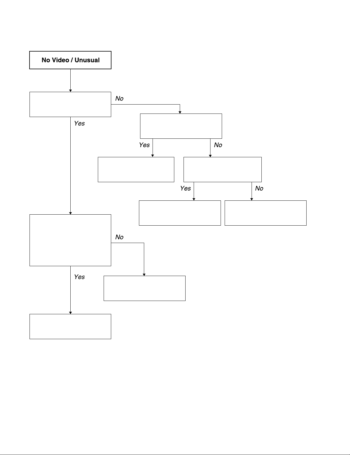
A
12345678910
28
Page 29

INVERTER Unit
J
I
H
CONTROL Unit LED Unit
G
LC-15B1U
TERMINAL Unit
F
E
D
C
B
A
12345678910
29
Page 30

LC-15B1U
Q
BLOCK DIAGRAMS
J
I2C
TUNER
TU3201
I
AV1
S-VIDEO
INPUT
H
G
F
E
D
AV2
INPUT
OUTPUT
COMPONENT
INPUT
DC IN
DC12V
DC/DC
T3701
IC3701
Q3700
Q3701
Q3702
LAMP
CHECK
TV- V
SIF
SY, SC
V1
L1, R1
L2, R2
Y, PB, PR
DL, DR
REGULATOR
38V
9V
5V
-8V
-20V
AUDIO
IN/OUT
SWITCH
IC3501
Q3500
DECODER
IC3702
AUDIO
(MSP)
IC3304
I2C
SIF-AMP.
Q3201
Q3202
31V
Q3707
29V
3704
8V
Q3706
V2/VO
VIDEO
IN/OUT
SWITCH
Q3501-Q3505
ANALOG UNIT
V2
VOUT
AUDIO
FILTER
IC3301
IC3302
IC3303
AUDIO
AMPLIFIER
IC3305
HEAD
PHONE
JACK
TV- V
V1
V2
VIDEO
SWITCH
IC402
SYNC
SEPARATER.
Q401
IC401
IREMI, POWOUT, TIMED
CVIN
CSYNC
L_ERR
BUFFER
Q402
5V REG.
IC703
SY, SC
MPU
IC2001
V
VIDEO
DECODER
(VPC)
IC801
3.3V REG.
CK, VD, HD, OSD-RGB
3 WIRE
BUS-SWITCH
KEY1, KEY2,PSWIN
RESET
IC2002
I2C
IC702
IC2003
E2PROM
IC2004
SUBDIN. SUBDOUT
C
Y
FIFO
IC1202
DAC
IC1101
IC1111
I2C
5V REG.
IC7102
BUFFER IC903
LCD
CONTROLLER
IC1201
GRADUATION
POWER FOR
IC1102-IC1108
COMMON
IC1113
IC1109
Q1101
Q1102
Q1108
Q1109
DIGITAL UNIT
3.3V REG.
CK,HBLK,VBLK
FLD,
LCD
IC1110
IC1112
IC1114
IC1115
IC901
LCD
POWER
TIMING
IC1116
Q1103
Q1104
Q1105
PC CARD
UNIT
LCD
PANEL
LC-15B1U
C
INVERTER UNIT
INVERTER
COLD
B
A
LAMPS
1234567891011 12 13 14 15 16 17 18 19 20
HOT
Q6500, Q6501
T6500, T6501
Q6503, Q6504
T6502, T6503
SP-L
SP-R
LED
D4014
D4015
RECEIVER
RMC4002
LED UNIT
R/C
POWER
SWITCH
CONTROL UNIT
CONTROL
KEYS
30~31
Page 31

LC-15B1U
DESCRIPTION OF SCHEMATIC DIAGRAM
IMPORTANT SAFETY NOTICE:
PARTS MARKED WITH
"å " ( )
ARE
INPORTANT FOR MAINTAINING THE SAFETY OF
THE SET.
BE SURE TO REPLACE THESE PARTS WITH
SPECIFIED ONES FOR MAINT AINING THE SAFETY
AND PERFORMANCE OF THE SET.
CAUTION:
This circuit diagram is original one, therefore there
may be a slight difference from yours.
1. When the exclusive-use AC adapter is used, the color
bar signal of color bar generator for service is input
to get the normal screen. When the audio is
minimized, the voltage value is measured with the
20 kΩ/V tester.
2. When the exclusive-use AC adapter is used, the color
density, lightness and color hue are set to the center
position, and the signal of color bar generator for
service is observed to get waveform.
The waveform test point is indicated with the mark
( ) in the wiring diagram.
AVIS DE SECURITE IMPORTANT:
LES PIECES MARQUEES
"å" ( )
SONT
IMPORTANTES POUR MAINTENIR LA SECURITE
DE L'APPAREIL.
NE REMPLACER CES PIECES QUE PAR DES
PIECES DONT LE NUMERO EST SPECIFIE POUR
MAINTENIR LA SECURITE ET PROTEGER LE
BON FONCTIONNEMENT DE L'APPAREIL.
3. Indication of resistors and capacitors
[Resistors]
Unit : Nonindication … Ω, K…kΩ,
M…MΩ
Error : Nonindication … ±5%
F…±1%
D…±0.5%
[Capacitor]
Unit :Nonindication or µ … µF,
P or p … pF
[Item]
Resistors
Nonindication Carbon-film resistor
C Solid resistor
S Metal-oxide-film resistor
N Metal-film resistor
W Cement resistor
T Special resistor
Capacitors
Nonndication Ceramic capacitor
ML Mylar capacitor
PF Polypropylene
film capacitor
TA Tantalum capacitor
ST Styrol capacitor
32
Page 32

SCHEMATIC DIAGRAMS
Ë
CONTROL Unit
J
I
H
G
LC-15B1U
F
Ë
LED Unit
E
D
C
B
A
12345678910
33
Page 33

LC-15B1U
LC-15B1U
Ë
MAIN Unit -1/4
DIGITAL 1
J
I
H
G
F
E
D
C
B
A
1234567891011 12 13 14 15 16 17 18 19 20
34~35
Page 34

LC-15B1U
LC-15B1U
Ë
MAIN Unit -2/4
DIGITAL 2
J
I
H
G
F
E
D
C
B
A
1234567891011 12 13 14 15 16 17 18 19 20
36~37
Page 35

LC-15B1U
LC-15B1U
Ë
MAIN Unit -3/4
DIGITAL 3
J
I
H
G
F
E
D
C
B
A
1234567891011 12 13 14 15 16 17 18 19 20
38~39
Page 36

LC-15B1U
LC-15B1U
Ë
MAIN Unit -4/4
DIGITAL 4
J
I
H
G
F
E
D
C
B
A
1234567891011 12 13 14 15 16 17 18 19 20
40~41
Page 37

LC-15B1U
Ë
TERMINAL Unit -1/2
LC-15B1U
å AND SHADED COMPONENTS=SAFETY RELATED PARTS
J
ANALOG 1
I
H
G
F
E
D
C
B
A
1234567891011 12 13 14 15 16 17 18 19 20
42~43
Page 38

LC-15B1U
Ë
TERMINAL Unit -2/2
LC-15B1U
å AND SHADED COMPONENTS=SAFETY RELATED PARTS
J
ANALOG 2
I
H
G
F
E
å
D
C
B
A
1234567891011 12 13 14 15 16 17 18 19 20
44~45
Page 39

LC-15B1U
Ë
INVERTER Unit
J
I
H
G
å AND SHADED COMPONENTS=SAFETY RELATED PARTS
å
å
F
E
D
C
B
A
12345678910
46
Page 40

- M E M O -
LC-15B1U
47
Page 41

LC-15B1U
PRINTED WIRING BOARD ASSEMBLIES
J
I
H
G
Ë
MAIN Unit Side-A (Component Parts)
F
E
D
C
B
A
12345678910
48
Page 42

LC-15B1U
Ë
J
I
H
G
MAIN Unit Side-B (Component Parts)
F
E
D
C
B
A
12345678910
49
Page 43

LC-15B1U
LC-15B1U
Ë
MAIN Unit Side A (Chip Parts)
J
I
R7102
C7107 FB7104 R2037
C7030
C7029
FL7002
C7056
R7030 R7022
C7124 C7102
C7106
C7033
R2036
R7019 R7020
Z1
C7103 FB7103
D1105
R1030
R1029
C1148 R1187
R1196
R1169
IC1104
IC1112
R1199
D1110
R1188
C1141
C1142
R1010
C1139
D1108
Q1103
P2004
Q2005
Q2006
R2055
R2026
R2044
R2045
R2017
R2018
R2019
C2016
C404
R1009
R1008
R1016
R1001
C1149
R1170
R1172
R1171
C1123
R1175
R1176
R1185
C1136
R1017
IC1113
R1007
R1006
C1130
R1157
Q1104
R1194
Q1105
R2020
R1015
R1161
R1107
C1147
R1112
R1114
R711
C711
R1154
R1195
C2015
R1013
R1133
R1186
C1138
C1137
R2047
R2038
Q712
D1109
R1118
R1111
C1144
IC1110
C2017
R1129
Q2007
R1183
C1135
R1014
C1101
R1024
R1106
IC1103
R2067
X2001
R1192
R2024
R2033
C2004 R2005
C1218
IC1105
R1184
R1193
C1134
C1114
C1113
C1125
R1160
R1108
R1110
C1104
R1163
R1162
C701
D701
C703
C7036
C7201
C702
R2050
D2003
D2002
C2021
IC402
C410
R424
R423
FL401
C7202
FL7003
R7202
R7201
FB7105
C7123
R7112
C7101
FL7001
R7001
C2022
R7106
C7108
R7016 R7021
R714
R705
C7105
C7104
H
SC2001
C2020
R422
G
C7122
F
C7054
D7701
C7046
R7203
C7204
C7205
R418
R417
IC7201
R419
C409
R415
C414
L402
C408
C413
R414
L401
C411
C412
R416
R425
Q403
C7203
R7204
IC7202
C7053
E
C7048
C7047
C7701
R7025
R7051
R7052
C7015
C7031
R7012
C7113
C7027
FB7003 FL7004
FB7004
D
R7048
R7043
R7042
C7055
FL7101
FL7102
C7059
IC7001
C7024
R7023 R7024
C
C7025
X7001
Q7001
C7005
R7003
R2023
R1117
C1112
D2004
C2005 R2006
R2062
R1152
R1164
R1190
R2027
IC2001
X2002
R1141
R1142
C1156
R1191 R1151
C706
R2022
Q2004
R1182
C1133
C1111
P2003
R726
R2057
C838
C1110
R1144 R1143
C1126
C2009
R1140 C1152
R1116
C1109
R2040
R2021
R2053
R2041
P2001
R712
R2060
R1153
R2056
C1230
Q1203
R1223
R1218
C1212
C1229
R1258
R1214
C1226
R1257
R1201
C1205
R1222
R1231
FB1202
SC1203
R1226
R826
R1232
L1204
C1213
FB1201
FD1
C1217
FB1203 R1208
C1234
R1209
C1227
C1216
C1208
C1228
IC1208
C821
R1211
R1260 R1210
R2061
R1127
R1131
R2054
R2002
R2063
R2028
R2031
C834
C1117
R1124
R1132
R2051
C2023
R2015
C1118
R1119
C1121
R1128
C1129
R1018
C908
D1106 Q1107
L1202
SC1201
R1019
L901
C901
R2032
R901
C909
SC901
R918
R916
C1206
R917
C1210
C1209
R1259
R1212
Q711
R2009
R2068
R2042
R2011
R2029
C2007
C826
L805
IC1109
R1125
R1126
R1115
R1189
C1107
C910
C1214
L902
C902
R1238
R1202 R1203
R1247
R1253
R1252
D1206
D1205
R1243
C1231
L804
C809
IC1201
C1211
C835
C801
R1204
SC1202
B
A
1234567891011 12 13 14 15 16 17 18 19 20
50~51
Page 44

LC-15B1U
LC-15B1U
Ë
MAIN Unit Side B (Chip Parts)
J
I
D1208
L1201
C1232
R1245
D1211
R1246D1210
Q1204
D1204
R1239
R1230
D1203
R1240
R1250
D1213
C1233
R1241
H
D1212
R1237
C1225
R1251
G
R1255
R1225
R1254
IC1207
Q1201
C1223C1224
C1204
IC1206
R1256
R834
R833
R832
L801
C824
R807
L803
C828
R809
C825
R808
L802
C808
C811
C827C830
C837C831
C836C832
C823C807
R811
R1221
R1234
R1233
C1201
R1220
C1203
R1217
R814
FB802
R804
R819
F
E
D
R1235
C
R1236
IC1202
FD2
C841
C840
C820
C819
R831
R838
R816
C822
C839
C1202
D902
R1248
R1249
Q1205
D1209
C817
C815
R815
C812
C816
C814
R812
R837
C810
TP801
TP802
IC801
C818
C813
R813
R810
C805
C806
R803R802R801
FB801
FB901FB903
R911
R912
C903
R915
C803
R836
X801
R835
C804
R906
C802
IC903
L1203
R902
C1215
IC901
D901
R910
R914
R913
R905
R904
R907
R909
R908
R919
C905
R1148R1147
L1205
R1021
C1151
C1155
C1207
R1020
R1123
C1122
IC2004
R2012
Q1102
Q1106
R1022
R1130
FB902
R2016
C2008
IC2003
C1108
R1023
R1122
TP2005
C1119
R2013R2014
D1107
Q1101
R2059
D1101
R1109R1173
R2058
R1120
IC1106
C705
C1102
R1121
R1145
C1116
C1120
R1198
C1153
IC1102
R1102
C2019R2010
R1158
TP2003
R1146
C2018
C1103
R1150
C2010
Q1108
Q1109
D1201
IC702
IC2002
R2007
IC1107
R1104
C1154
C2006
R2043
R2049
R1031
R2003
R1228
R2001
IC1108
IC1101
R1032
TP2001
TP2002
C2002
C2003
R1033
C1124
C2001
R2066
R2064
R403
C1115
R2030
R1134
R402
C407
R1025
TP2007
R1026
IC1116
R401
IC1114
TP2006
TP2009
IC401
C405
R410
C1146
R1156
R1155
R2065D2005
R407
R406
C1145
Q402
R411
Q401
C406
R409
R408
C403
C401
R1002
C1150
C1157
R1003
R1005
IC1111
R1027
R1028
C1132
IC1115
Z2
IC703
R2052
R413
R412
R404
C402R405
R1177R1174
R1034
C1131
C1143
R1179
R1178
C1105
R1168
R1167
R1166
C7050
Q7006
IC7003
R7031
R7032
IC7101
R7033
R7014
Q7005
FB7002
R7011
C7111
R7015
C7026
R7010
FB7001
R7017R7018
R7049
C7085
C7112
R7013
Q7004
IC7004
R7101
C7028
R7009
Q7003
Q7101Q7102
R7046
R7008
R7036
C7037
C7038
R7034
Q7002R7006
R7045
R7044
R7035
R7007
FB7101
R7103R7104
R7002
FB7102
Q7007
L7002
Q7008
C7061
C7008
C7012
C7006
C7009
C7007
C7013
R7005
R7004
C7010
TP7002
C7060
C7041
C7014
TP7001
C7058
L7001
C7032
C7004
R7037
R7039
C7042
C7043
C7035
R7041
C7016
C7017
R7040
C7022
C7018
R7038
C7062
Q7009
Q7010
C7019
C7020
R716
R715
R7053
C7003
L7003
C7021
C7002
C7072
R717
R719
R7113
C7023
R7029
R7705
R7704
R7047
R7702
R7703
IC7701
R7701
C7001
C7702
IC7002
C7121
R7114
R7110
IC7102
R7050
B
A
1234567891011 12 13 14 15 16 17 18 19 20
52~53
Page 45

LC-15B1U
J
I
H
G
Ë
Terminal Unit Side-A (Component Parts)
F
E
D
C
B
A
12345678910
54
Page 46

LC-15B1U
Ë
J
I
H
G
Terminal Unit Side-B (Component Parts)
F
E
D
C
B
A
12345678910
55
Page 47

LC-15B1U
LC-15B1U
Ë
TERMINAL Unit Side A (Chip Parts)
J
I
H
G
F
E
D
C
B
A
1234567891011 12 13 14 15 16 17 18 19 20
56~57
Page 48

LC-15B1U
J
I
H
G
Ë
Control Unit Side-A (Component Parts)
Ë
Inverter Unit Side-A (Component Parts)
F
E
D
Ë
LED Unit Side-A (Component Parts)
C
B
A
12345678910
58
Page 49

LC-15B1U
Ë
Control Unit Side-B (Component Parts)
J
I
H
Ë
Inverter Unit Side-B (Component Parts)
G
F
E
D
Ë
LED Unit Side-B (Component Parts)
C
B
A
12345678910
59
Page 50

LC-15B1U
LC-15B1U
Ë
CONTROL Unit Side A (Chip Parts)
J
I
H
Ë
INVERTER Unit Side A (Chip Parts)
G
F
E
D
Ë
LED Unit Side A (Chip Parts)
C
B
A
1234567891011 12 13 14 15 16 17 18 19 20
60~61
Page 51

LC-15B1U
Ref. No. Part No. ★ Description Code
PARTS LIST
PARTS REPLACEMENT
Replacement parts which have these special safety characteristics identified in this manual: electrical components having
such features are identified by
Replacement Parts Lists and schematic diagrams.
The use of a substitute replacement part which does not have
the same safety characteristics as the factory recommended
replacement parts shown in this service manual may create
shock, fire or other hazards.
“
HOW TO ORDER REPLACEMENT PARTS
To have your order filled promptly and correctly, please furnish
the following informations.
1. MODEL NUMBER 2. REF. NO.
3. PART NO. 4. DESCRIPTION
in USA : Contact your nearest SHARP Parts Distributor to order.
For location of SHARP Parts Distributor, please call TollFree: 1-800-BE SHARP
MARK★: SPARE PARTS-DELIVERY SECTION
“å”
and shaded area in the
”
Ref. No. Part No. ★ Description Code
LISTE DES PIECES
CHANGE DES PIECES
Les pièces de rechange qui présentent ces caractéristiques spéciales
de sécurité, sont identifiées dans ce manuel : les pièces électriques
qui présentent ces particularités, sont repérée par la marque "å" et
sont hachurées dans les listes de pièces et dans les diagrammes sch
ématiques.
La substitution d'une pièce de rechange par une autre qui ne présente
pas les mêmes caractéristiques de sécurité que la pièce recommandée par l'usine et repérée dans ce manuel de service, peut provoquer
une électrocution, un incendie ou tout autre sinistre.
“
COMMENT COMMANDER LES PIECES DE RECHANGE
Pour que votre commande soit rapidement et correctement remplie,
veuillez fournir les renseignements suivants.
1. NUMERO DU MODELE 2. NO. DE REF
3. NO. DE PIECE 4. DESCRIPTION
in CANADA : Contact SHARP Electronics of Canada Limited.
Phone: (416) 890-2100
★MARQUE: SECTION LIVRAISON DES PIECES DE RECHANGE
”
LCD PANEL UNIT
RLCDTA013WJZZ J 15' LCD Panel Unit DB
PRINTED WIRING BOARD ASSEMBLIES
(NOT REPLACEMENT ITEM)
DUNTKA670FE23 - MAIN PWB Unit —
DUNTKB128DE05 - TERMINAL PWB Unit —
DUNTKB129DE05 - CONTROL PWB Unit —
DUNTKB130DE05 - LED PWB Unit —
DUNTKB131DE05 - INVERTER PWB Unit —
DUNTKB021CEN1 J PC CARD Unit
(Unit replacement)
Ref. No. Part No. ★ Description CodeRef. No. Part No. ★ Description Code
DUNTKA670FE23
MAIN PWB Unit
INTEGRATED CIRCUITS
IC401 VHiBA7046F/-1 J BA7046F AF
IC402 VHiNJM2235V-1 J NJM2235V AE
IC702 VHiBA033FP/-1 J BA033FP-E2 AG
IC703 VHiPQ20VZ11-1 J PQ20VZ11 AH
IC801 VHiVPC3230D1EQ J VPC3230D-QA-B3 BD
IC901 VHiPQ1CZ21H-1Y J PQ1CZ21H2ZP AH
IC903 VHiVHC541FT-1Y J TC74VHC541FT AK
IC1101 VHiMB8346BV-1 J MB88346BPFV AN
IC1102 VHiNJM4565V-1 J NJM4565V AF
IC1103 VHiNJM2060V-1 J NJM2060V AF
IC1104 VHiNJM2060V-1 J NJM2060V AF
IC1105 VHiBU4053V/-1 J BU4053BCFV-E2 AE
IC1106 VHiNJM4580V-1 J NJM4580V AE
IC1107 VHiNJM4580V-1 J NJM4580V AE
IC1108 VHiNJM4580V-1 J NJM4580V AE
IC1109 VHiNJM353M/-1 J NJM353M AG
IC1110 VHiBU4053V/-1 J BU4053BCFV-E2 AE
IC1111 VHiMB8346BV-1 J MB88346BPFV AN
IC1112 VHiBU4053V/-1 J BU4053BCFV-E2 AE
IC1113 VHiBU4053V/-1 J BU4053BCFV-E2 AE
IC1114 VHiNJM4580V-1 J NJM4580V AE
IC1115 VHiNJM4580V-1 J NJM4580V AE
IC1116 VHiNJM2147M-1 J NJM2147M-TE1 AF
IC1201 RH-iX3378CEN1Q J LR38815 AY
IC1202 VHiPD485505-2 J UPD485505G-25 AY
IC1206 VHiLVX125FT-1 J TC74LVX125F AG
IC1207 VHiTC4W66U/-1 J TC4W66FU AF
IC1208 VHiPQ1R34++-1Y J PQ1R34 AE
IC2001 RH-iXA276WJZZQ J M306V0ME-164FP BA
IC2002 VHiBD4746G+-1Y J BD4746G-TR AD
IC2003 VHiTC4W66U/-1 J TC4W66FU AF
IC2004 VHiBR2416E2-1 J BR24C16F AK
IC7102 VHiPQ05TZ11-1 J PQ05TZ11 AH
Q401 VS2SC3928AR-1 J 2SC3928AR AB
Q402 VS2SA1037KQ-1 J 2SA1037KQ AA
62
TRANSISTORS
Page 52

LC-15B1U
Ref. No. Part No. ★ Description Code Ref. No. Part No. ★ Description Code
DUNTKA670FE23
MAIN PWB Unit (Continued)
Q711 VS2SA1037KQ-1 J 2SA1037KQ AA
Q712 VSDTC144EE/-1 J DTC144EE AA
Q1101 VS2SA1729//-1 J 2SA1729 AF
Q1102 VS2SC4520//-1 J 2SC4520 AE
Q1103 VS2SA1036K/-1 J 2SA1036K AC
Q1104 VS2SA1036K/-1 J 2SA1036K AC
Q1105 VS2SA1036K/-1 J 2SA1036K AC
Q1106 VSFMMT718//-1 J FMMT718 AE
Q1107 VSDTC144EE/-1 J DTC144EE AA
Q1108 VS2SC4520//-1 J 2SC4520 AE
Q1109 VS2SA1729//-1 J 2SA1729 AF
Q1201 VSDTC144EE/-1 J DTC144EE AA
Q1203 VSDTC144EE/-1 J DTC144EE AA
Q1204 VS2SA1037KQ-1 J 2SA1037KQ AA
Q1205 VSUMX2N++++-1Y J UMX2N++++ AB
Q2004 VSDTC114EE/-1 J DTC114EE AB
Q2007 VSDTC144EE/-1 J DTC144EE AA
DIODES
D701 VHDDAN202K/-1 J DAN202K AB
D901 VHDDAN222//-1 J DAN222 AA
D902 VHDSFPB74//2E J SFPB74 AD
D1101 VHD1SS250//1E J 1SS250 AB
D1106 VHDDAN222//-1 J DAN222 AA
D1107 VHD1SS250//1E J 1SS250 AB
D1108 VHDDAN222//-1 J DAN222 AA
D1109 VHDDAN222//-1 J DAN222 AA
D1110 VHDDAN222//-1 J DAN222 AA
D1201 VHD1SS250//1E J 1SS250 AB
D1203 VHDRB491D++-1Y J RB491D++ AD
D1205 VHDDAN222//-1 J DAN222 AA
D1206 RH-EX0227CEZZ J Zener, EX0227CE AB
D1208 VHDDAN222//-1 J DAN222 AA
D1209 RH-EX1247CEZZY J Zener, EX1247CE AB
D1210 VHDDAN222//-1 J DAN222 AA
D1211 VHDDAN222//-1 J DAN222 AA
D1212 VHDRB481K++-1Y J RB481K++ AD
D2002 VHDRB491D++-1Y J RB491D++ AD
D2004 RH-DX0061GEZZ J DX0061GE AC
PACKAGED CIRCUIT
X801 RCRSC0012CEZZ J Crystal, CRSC0012CE AH
FILTER
X2002 RFiLZ0169TAZZY J Filter, FiLZ0169TA AD
COILS
L401 VP-9N4R7KR56N J Peaking 4.7µHAC
L402 VP-9N4R7KR56N J Peaking 4.7µHAC
L801 VP-9N3R3KR46N J Peaking 3.3µHAC
L802 VP-9N3R3KR46N J Peaking 3.3µHAC
L803 VP-9N3R3KR46N J Peaking 3.3µHAC
L804 RCiLC0055CEZZ J Coil, 100µHAD
L805 RCiLC0055CEZZ J Coil, 100µHAD
L901 RCiLC0055CEZZ J Coil, 100µHAD
L902 RCiLP0303TAZZ J Coil, 100µHAG
L1201 VP-1M470J5R4N J Peaking 47µHAC
L1202 RCiLC0055CEZZ J Coil, 100µHAD
L1203 VP-1M220J2R9N J Peaking 22µHAC
L1204 VP-1M220J2R9N J Peaking 22µHAC
L1205 VP-1M220J2R9N J Peaking 22µHAC
CAPACITORS
C401 VCKYTV1AB105K J 1 10V Ceramic AD
C402 VCKYCY1HB102K J 1000p 50V Ceramic AA
C403 VCKYCY1EF104Z J 0.1 25V Ceramic AA
C404
C405 VCKYCY1HB222K J 2200p 50V Ceramic AA
C406 VCKYTV1AB105K J 1 10V Ceramic AD
C407 VCCCCY1HH101J J 100p 50V Ceramic AA
C408 VCKYTV1AB105K J 1 10V Ceramic AD
VCEASM0JW476MY
J 47 6.3V Electrolytic AC
C409 VCKYTV1AB105K J 1 10V Ceramic AD
C410 VCKYCY1EF104Z J 0.1 25V Ceramic AA
C411 VCKYTV1AB105K J 1 10V Ceramic AD
C412 VCCCCY1HH331J J 330p 50V Ceramic AA
C413 VCCCCY1HH331J J 330p 50V Ceramic AA
C414 VCCCCY1HH331J J 330p 50V Ceramic AA
C701 VCKYTV1CF105Z J 1 16V Ceramic AB
C702
C703 VCKYTV1CF105Z J 1 16V Ceramic AB
C705 VCKYCY1CF334Z J 0.33 16V Ceramic AA
C706
C711 VCKYCY1EF104Z J 0.1 25V Ceramic AA
C801
C802 VCKYCY1EF104Z J 0.1 25V Ceramic AA
C803 VCCCCY1HH7R0D J 7p 50V Ceramic AA
C804 VCCCCY1HH7R0D J 7p 50V Ceramic AA
C805 RC-KZ1025CEZZ J 1 10V Ceramic AB
C806 RC-KZ1025CEZZ J 1 10V Ceramic AB
C807 VCKYCY1HB331K J 330p 50V Ceramic AA
C808 VCKYCY1HB331K J 330p 50V Ceramic AA
C809
C810 VCKYCY1EF104Z J 0.1 25V Ceramic AA
C811 VCKYCY1HB331K J 330p 50V Ceramic AA
C812 RC-KZ1025CEZZ J 1 10V Ceramic AB
C813 RC-KZ1025CEZZ J 1 10V Ceramic AB
C814 VCKYCY1HB102K J 1000p 50V Ceramic AA
C815 VCKYTV1CF684Z J 0.68 16V Ceramic AB
C816 VCKYTV1CF684Z J 0.68 16V Ceramic AB
C817 VCKYTV1CF684Z J 0.68 16V Ceramic AB
C818 RC-KZ1025CEZZ J 1 10V Ceramic AB
C819 RC-KZ1025CEZZ J 1 10V Ceramic AB
C820 VCKYCY1EF104Z J 0.1 25V Ceramic AA
C821
C822 RC-KZ1025CEZZ J 1 10V Ceramic AB
C823 RC-KZ1025CEZZ J 1 10V Ceramic AB
C824 VCKYCY1AB224K J 0.22 10V Ceramic AB
C825 VCKYCY1AB224K J 0.22 10V Ceramic AB
C826
C827 VCKYCY1EF104Z J 0.1 25V Ceramic AA
C828 VCKYCY1AB224K J 0.22 10V Ceramic AB
C830 VCKYCY1CF224Z J 0.22 16V Ceramic AA
C831 VCKYCY1CF224Z J 0.22 16V Ceramic AA
C832 VCKYCY1CF224Z J 0.22 16V Ceramic AA
C834 VCKYCY1EF104Z J 0.1 25V Ceramic AA
C835
C836 RC-KZ1025CEZZ J 1 10V Ceramic AB
C837 RC-KZ1025CEZZ J 1 10V Ceramic AB
C838
C839 RC-KZ1025CEZZ J 1 10V Ceramic AB
C840 VCKYTV1CF684Z J 0.68 16V Ceramic AB
C901
C902
C903 VCKYCY1CF334Z J 0.33 16V Ceramic AA
C905 VCKYCY1EF104Z J 0.1 25V Ceramic AA
C908
C909 VCKYCY1CF334Z J 0.33 16V Ceramic AA
C910
C1101 VCKYCY1EF104Z J 0.1 25V Ceramic AA
C1102 VCKYCY1EF104Z J 0.1 25V Ceramic AA
C1103 VCKYCY1EF104Z J 0.1 25V Ceramic AA
C1104 VCKYCY1EF104Z J 0.1 25V Ceramic AA
C1105 VCKYCY1EF104Z J 0.1 25V Ceramic AA
C1107 VCKYCY1EF104Z J 0.1 25V Ceramic AA
C1108 VCKYCY1EF104Z J 0.1 25V Ceramic AA
C1109 VCKYCY1EF104Z J 0.1 25V Ceramic AA
C1110 VCKYCY1EF104Z J 0.1 25V Ceramic AA
C1111 VCKYCY1EF104Z J 0.1 25V Ceramic AA
C1112 VCKYCY1EF104Z J 0.1 25V Ceramic AA
C1113 VCKYCY1EF104Z J 0.1 25V Ceramic AA
C1114 VCKYCY1EF104Z J 0.1 25V Ceramic AA
C1115 VCKYCY1EF104Z J 0.1 25V Ceramic AA
C1116 VCKYCY1EF104Z J 0.1 25V Ceramic AA
C1117 VCCCCY1HH560J J 56p 50V Ceramic AA
C1118 VCKYCY1EF104Z J 0.1 25V Ceramic AA
C1119 VCKYTV1CF105Z J 1 16V Ceramic AB
VCEASM1CN226MY
VCEASM0JN226MY
VCEASM1CN106MY
VCEASM1CN107MY
VCEASM1CN107MY
VCEASM0GW227MY
VCEASM1CW107MY
VCEASM0GW107MY
VCAAPC1CJ826MY
VCEASH0JN337MY
VCEASM1CW107MY
VCAAPC1CJ396MY
J 22 16V Electrolytic AD
J 22 6.3V Electrolytic AC
J 10 16V Electrolytic AC
J 100 16V Electrolytic AD
J 100 16V Electrolytic AD
J 220 4V Electrolytic AC
J 100 16V Electrolytic AD
J 100 4V Electrolytic AC
J 82 16V Electrolytic AH
J 330 6.3V Electrolytic AC
J 100 16V Electrolytic AD
J 39 16V Electrolytic AG
63
Page 53

LC-15B1U
Ref. No. Part No. ★ Description Code
DUNTKA670FE23
MAIN PWB Unit (Continued)
C1120 VCKYTV1EF104Z J 0.1 25V Ceramic AB
C1122 VCKYTV1CF105Z J 1 16V Ceramic AB
C1123 VCKYCY1EF104Z J 0.1 25V Ceramic AA
C1124 VCKYCY1EF104Z J 0.1 25V Ceramic AA
C1125
C1126 RC-EZ1339CEZZ J 220 16V Electrolytic AD
C1130 VCKYCY1EF104Z J 0.1 25V Ceramic AA
C1131 VCKYCY1EF104Z J 0.1 25V Ceramic AA
C1132 VCKYCY1EF104Z J 0.1 25V Ceramic AA
C1133 VCKYCY1EF104Z J 0.1 25V Ceramic AA
C1134 VCKYCY1EF104Z J 0.1 25V Ceramic AA
C1135 VCKYCY1EF104Z J 0.1 25V Ceramic AA
C1136 VCKYCY1EF104Z J 0.1 25V Ceramic AA
C1137 VCKYCY1EF104Z J 0.1 25V Ceramic AA
C1138 VCKYCY1EF104Z J 0.1 25V Ceramic AA
C1139 VCKYCY1EF104Z J 0.1 25V Ceramic AA
C1141 VCKYCY1EF104Z J 0.1 25V Ceramic AA
C1142 VCKYCY1EF104Z J 0.1 25V Ceramic AA
C1143 VCKYCY1EF104Z J 0.1 25V Ceramic AA
C1144 VCKYCY1EF104Z J 0.1 25V Ceramic AA
C1145 VCKYCY1EF104Z J 0.1 25V Ceramic AA
C1146 VCKYCY1EF104Z J 0.1 25V Ceramic AA
C1147 VCKYCY1EF104Z J 0.1 25V Ceramic AA
C1148 VCKYCY1EF104Z J 0.1 25V Ceramic AA
C1149 VCKYCY1EF104Z J 0.1 25V Ceramic AA
C1150 VCKYCY1EF104Z J 0.1 25V Ceramic AA
C1151 VCKYCY1EF104Z J 0.1 25V Ceramic AA
C1152 VCCCCY1HH181J J 180p 50V Ceramic AA
C1153 VCKYTV1HB103K J 0.01 50V Ceramic AA
C1154 VCKYTV1HB103K J 0.01 50V Ceramic AA
C1155 VCKYTV1CB334K J 0.33 16V Ceramic AC
C1156 VCCCCY1HH560J J 56p 50V Ceramic AA
C1157 VCKYTV1CB105K J 1 16V Ceramic AC
C1202 VCKYCY1EF104Z J 0.1 25V Ceramic AA
C1203 VCKYCY1EF104Z J 0.1 25V Ceramic AA
C1204 VCCCCY1HH220J J 22p 50V Ceramic AA
C1205 VCCCCY1HH220J J 22p 50V Ceramic AA
C1206
C1207 VCKYCY1EF104Z J 0.1 25V Ceramic AA
C1208 VCKYTV1HF104Z J 0.1 50V Ceramic AA
C1209
C1210
C1211 VCKYCY1EF104Z J 0.1 25V Ceramic AA
C1212 VCKYCY1EF104Z J 0.1 25V Ceramic AA
C1213
C1214
C1215 RC-KZ1025CEZZ J 1 10V Ceramic AB
C1217
C1218
C1223 VCKYCY1EF104Z J 0.1 25V Ceramic AA
C1224 VCKYCY1EF104Z J 0.1 25V Ceramic AA
C1225 VCKYCY1EF104Z J 0.1 25V Ceramic AA
C1226
C1227 VCKYTV1CB105K J 1 16V Ceramic AC
C1228 RC-KZ1025CEZZ J 1 10V Ceramic AB
C1229
C1230 VCKYTV1CB105K J 1 16V Ceramic AC
C1231
C1232 VCKYTV1HF104Z J 0.1 50V Ceramic AA
C2001 VCKYCY1HB102K J 1000p 50V Ceramic AA
C2002 VCCCCY1HH221J J 220p 50V Ceramic AA
C2003 VCKYTV1AB105K J 1 10V Ceramic AD
C2006 RC-KZ1025CEZZ J 1 10V Ceramic AB
C2007 VCKYCY1EF104Z J 0.1 25V Ceramic AA
C2009 VCKYCY1EF104Z J 0.1 25V Ceramic AA
C2010 VCKYCY1EF104Z J 0.1 25V Ceramic AA
C2015 VCKYCY1HB561K J 560p 50V Ceramic AA
C2016 VCKYCY1EF104Z J 0.1 25V Ceramic AA
C2017 VCKYCY1EF104Z J 0.1 25V Ceramic AA
C2018 VCCCCY1HH220J J 22p 50V Ceramic AA
C2020 VCKYCY1HB271K J 270p 50V Ceramic AA
VCEASM1CN107MY
VCEASM1HN106MY
VCEASH0JN227MY
VCEASM0GW107MY
VCEASM1CW107MY
VCEASM0GW107MY
VCEASM1HN475MY
VCEASM1CN106MY
VCEASM1HN106MY
VCEASM1CN226MY
VCEASM1CN107MY
J 100 16V Electrolytic AD
J 10 50V Electrolytic AD
J 220 6.3V Electrolytic AC
J 100 4V Electrolytic AC
J 100 16V Electrolytic AD
J 100 4V Electrolytic AC
J 4.7 50V Electrolytic AD
J 10 16V Electrolytic AC
J 10 50V Electrolytic AD
J 22 16V Electrolytic AD
J 100 16V Electrolytic AD
Ref. No. Part No. ★ Description Code
C2021
C2023
C7054 VCKYCY1HB103K J 0.01 50V Ceramic AA
C7104
C7105 VCKYCY1EF104Z J 0.1 25V Ceramic AA
C7121 VCKYTV1CF105Z J 1 16V Ceramic AB
C7122
VCEASM1CW107MY
VCEASM1CN106MY
VCEASM1CN107MY
VCEASM1CN107MY
J 100 16V Electrolytic AD
J 10 16V Electrolytic AC
J 100 16V Electrolytic AD
J 100 16V Electrolytic AD
RESISTORS
R401 VRS-CY1JF104J J 100k 1/16W Metal Oxide AA
R402 VRS-CY1JF333J J 33k 1/16W Metal Oxide AA
R403 VRS-CY1JF103J J 10k 1/16W Metal Oxide AA
R404 VRS-CY1JF101J J 100 1/16W Metal Oxide AA
R405 VRS-CY1JF562J J 5.6k 1/16W Metal Oxide AA
R406 VRS-CY1JF332J J 3.3k 1/16W Metal Oxide AA
R407 VRS-CY1JF101J J 100 1/16W Metal Oxide AA
R408 VRS-CY1JF332J J 3.3k 1/16W Metal Oxide AA
R409 VRS-CY1JF103J J 10k 1/16W Metal Oxide AA
R410 VRS-CY1JF474J J 470k 1/16W Metal Oxide AA
R412 VRS-CY1JF562J J 5.6k 1/16W Metal Oxide AA
R414 VRS-CY1JF105J J 1M 1/16W Metal Oxide AA
R415 VRS-CY1JF105J J 1M 1/16W Metal Oxide AA
R416 VRS-CY1JF105J J 1M 1/16W Metal Oxide AA
R417 VRS-CY1JF101J J 100 1/16W Metal Oxide AA
R418 VRS-CY1JF101J J 100 1/16W Metal Oxide AA
R419 VRS-CY1JF101J J 100 1/16W Metal Oxide AA
R423 VRS-CY1JF000J J 0 1/16W Metal Oxide AA
R705 VRS-CY1JF1R0J J 1 1/16W Metal Oxide AA
R711 VRS-CY1JF103J J 10k 1/16W Metal Oxide AA
R712 VRS-CY1JF103J J 10k 1/16W Metal Oxide AA
R714 VRS-CY1JF1R0J J 1 1/16W Metal Oxide AA
R715 VRS-CY1JF103J J 10k 1/16W Metal Oxide AA
R716 VRS-CY1JF102J J 1k 1/16W Metal Oxide AA
R717 VRS-CY1JF332J J 3.3k 1/16W Metal Oxide AA
R726 VRS-CY1JF1R0J J 1 1/16W Metal Oxide AA
R801 VRS-CB1JF221J J 220 1/16W Metal Oxide AC
R802 VRS-CB1JF220J J 22 1/16W Metal Oxide AC
R803 VRS-CB1JF220J J 22 1/16W Metal Oxide AC
R804 VRS-CA1JF101J J 100 1/16W Metal Oxide AA
R807 VRS-CY1JF750J J 75 1/16W Metal Oxide AA
R808 VRS-CY1JF750J J 75 1/16W Metal Oxide AA
R809 VRS-CY1JF750J J 75 1/16W Metal Oxide AA
R810 VRS-CB1JF220J J 22 1/16W Metal Oxide AC
R811 VRS-CY1JF222J J 2.2k 1/16W Metal Oxide AA
R812 VRS-CY1JF000J J 0 1/16W Metal Oxide AA
R813 VRS-CB1JF220J J 22 1/16W Metal Oxide AC
R814 VRS-CY1JF332J J 3.3k 1/16W Metal Oxide AA
R815 VRS-CY1JF101J J 100 1/16W Metal Oxide AA
R816 VRS-CY1JF470J J 47 1/16W Metal Oxide AA
R819 VRS-CY1JF000J J 0 1/16W Metal Oxide AA
R826 VRS-CY1JF101J J 100 1/16W Metal Oxide AA
R831 VRS-CY1JF102J J 1k 1/16W Metal Oxide AA
R832 VRS-CY1JF102J J 1k 1/16W Metal Oxide AA
R833 VRS-CY1JF102J J 1k 1/16W Metal Oxide AA
R834 VRS-CY1JF102J J 1k 1/16W Metal Oxide AA
R836 VRS-CY1JF000J J 0 1/16W Metal Oxide AA
R838 VRS-CY1JF000J J 0 1/16W Metal Oxide AA
R901 VRS-CY1JF000J J 0 1/16W Metal Oxide AA
R902 VRS-CY1JF000J J 0 1/16W Metal Oxide AA
R906 VRS-CY1JF000J J 0 1/16W Metal Oxide AA
R907 VRS-CY1JF000J J 0 1/16W Metal Oxide AA
R909 VRS-CY1JF104J J 100k 1/16W Metal Oxide AA
R910 VRS-CY1JF101J J 100 1/16W Metal Oxide AA
R911 VRS-CY1JF272F J 2.7k 1/16W Metal Oxide AA
R912 VRS-CY1JF162F J 1.6k 1/16W Metal Oxide AA
R913 VRS-CY1JF000J J 0 1/16W Metal Oxide AA
R914 VRS-CY1JF222J J 2.2k 1/16W Metal Oxide AA
R915 VRS-CY1JF332J J 3.3k 1/16W Metal Oxide AA
R916 VRS-CY1JF104J J 100k 1/16W Metal Oxide AA
R917 VRS-CY1JF104J J 100k 1/16W Metal Oxide AA
R918 VRS-CY1JF104J J 100k 1/16W Metal Oxide AA
R919 VRS-CY1JF333J J 33k 1/16W Metal Oxide AA
R1001 VRS-CY1JF102J J 1k 1/16W Metal Oxide AA
R1002 VRS-CY1JF103F J 10k 1/16W Metal Oxide AA
64
Page 54

LC-15B1U
Ref. No. Part No. ★ Description Code Ref. No. Part No. ★ Description Code
DUNTKA670FE23
MAIN PWB Unit (Continued)
R1003 VRS-CY1JF103F J 10k 1/16W Metal Oxide AA
R1005 VRS-CY1JF103F J 10k 1/16W Metal Oxide AA
R1006 VRS-CY1JF243F J 24k 1/16W Metal Oxide AA
R1007 VRS-CY1JF563F J 56k 1/16W Metal Oxide AA
R1008 VRS-CY1JF822F J 8.2k 1/16W Metal Oxide AA
R1009 VRS-CY1JF682F J 6.8k 1/16W Metal Oxide AA
R1013 VRS-CY1JF101J J 100 1/16W Metal Oxide AA
R1014 VRS-CY1JF103J J 10k 1/16W Metal Oxide AA
R1016 VRS-CY1JF103J J 10k 1/16W Metal Oxide AA
R1017 VRS-CY1JF272J J 2.7k 1/16W Metal Oxide AA
R1019 VRS-CY1JF473J J 47k 1/16W Metal Oxide AA
R1020 VRS-CY1JF472J J 4.7k 1/16W Metal Oxide AA
R1021 VRS-TW2ED102J J 1k 1/4W Metal Oxide AA
R1022 VRS-CY1JF000J J 0 1/16W Metal Oxide AA
R1024 VRS-CY1JF123F J 12k 1/16W Metal Oxide AA
R1025 VRS-CY1JF123F J 12k 1/16W Metal Oxide AA
R1026 VRS-CY1JF123F J 12k 1/16W Metal Oxide AA
R1027 VRS-CY1JF123F J 12k 1/16W Metal Oxide AA
R1028 VRS-CY1JF123F J 12k 1/16W Metal Oxide AA
R1029 VRS-CY1JF123F J 12k 1/16W Metal Oxide AA
R1030 VRS-TW2ED150J J 15 1/4W Metal Oxide AB
R1031 VRS-CY1JF000J J 0 1/16W Metal Oxide AA
R1032 VRS-CY1JF000J J 0 1/16W Metal Oxide AA
R1033 VRS-CY1JF000J J 0 1/16W Metal Oxide AA
R1034 VRS-CY1JF000J J 0 1/16W Metal Oxide AA
R1102 VRS-CY1JF103F J 10k 1/16W Metal Oxide AA
R1104 VRS-CA1JF333J J 33k 1/16W Metal Oxide AA
R1106 VRS-CF1JP333JY J 33k 1/16W Metal Oxide AC
R1107 VRS-CY1JF123F J 12k 1/16W Metal Oxide AA
R1108 VRS-CY1JF103F J 10k 1/16W Metal Oxide AA
R1109 VRS-CY1JF333J J 33k 1/16W Metal Oxide AA
R1110 VRS-CY1JF104F J 100k 1/16W Metal Oxide AA
R1111 VRS-CY1JF683F J 68k 1/16W Metal Oxide AA
R1112 VRS-CY1JF123F J 12k 1/16W Metal Oxide AA
R1114 VRS-CY1JF103F J 10k 1/16W Metal Oxide AA
R1115 VRS-CY1JF102J J 1k 1/16W Metal Oxide AA
R1116 VRS-CY1JF102J J 1k 1/16W Metal Oxide AA
R1117 VRS-CY1JF102J J 1k 1/16W Metal Oxide AA
R1118 VRS-CY1JF563F J 56k 1/16W Metal Oxide AA
R1119 VRS-CY1JF472F J 4.7k 1/16W Metal Oxide AA
R1120 VRS-TX2HF5R6J J 5.6 1/2W Metal Oxide AA
R1121 VRS-CY1JF181J J 180 1/16W Metal Oxide AA
R1123 VRS-CY1JF181J J 180 1/16W Metal Oxide AA
R1124 VRS-CY1JF472F J 4.7k 1/16W Metal Oxide AA
R1125 VRS-TX2HF101J J 100 1/2W Metal Oxide AA
R1126 VRS-CY1JF000J J 0 1/16W Metal Oxide AA
R1127 VRS-TX2HF1R8JY J 1.8 1/2W Metal Oxide AB
R1128 VRS-CY1JF105J J 1M 1/16W Metal Oxide AA
R1129 VRS-CY1JF363F J 36k 1/16W Metal Oxide AA
R1130 VRS-TX2HF5R6J J 5.6 1/2W Metal Oxide AA
R1131 VRS-CY1JF105J J 1M 1/16W Metal Oxide AA
R1132 VRS-CY1JF000J J 0 1/16W Metal Oxide AA
R1134 VRS-CY1JF000J J 0 1/16W Metal Oxide AA
R1140 VRS-CY1JF273F J 27k 1/16W Metal Oxide AA
R1142 VRS-CY1JF103F J 10k 1/16W Metal Oxide AA
R1143 VRS-CY1JF391J J 390 1/16W Metal Oxide AA
R1144 VRS-CY1JF391J J 390 1/16W Metal Oxide AA
R1145 VRS-TW2ED5R6J J 5.6 1/4W Metal Oxide AA
R1146 VRS-TW2ED8R2J J 8.2 1/4W Metal Oxide AB
R1147 VRS-TX2HF000J J 0 1/2W Metal Oxide AA
R1148 VRS-TX2HF100J J 10 1/2W Metal Oxide AA
R1150 VRS-CY1JF103F J 10k 1/16W Metal Oxide AA
R1151 VRS-CY1JF103F J 10k 1/16W Metal Oxide AA
R1152 VRS-CY1JF391J J 390 1/16W Metal Oxide AA
R1153 VRS-CY1JF680J J 68 1/16W Metal Oxide AA
R1154 VRS-CY1JF683F J 68k 1/16W Metal Oxide AA
R1157 VRS-CY1JF683F J 68k 1/16W Metal Oxide AA
R1158 VRS-CY1JF103F J 10k 1/16W Metal Oxide AA
R1160 VRS-CY1JF103F J 10k 1/16W Metal Oxide AA
R1161 VRS-CY1JF103F J 10k 1/16W Metal Oxide AA
R1162 VRS-CY1JF103F J 10k 1/16W Metal Oxide AA
R1163 VRS-CY1JF123F J 12k 1/16W Metal Oxide AA
R1164 VRS-CY1JF000J J 0 1/16W Metal Oxide AA
R1166 VRS-CY1JF104F J 100k 1/16W Metal Oxide AA
R1167 VRS-CY1JF103F J 10k 1/16W Metal Oxide AA
R1168 VRS-CY1JF103F J 10k 1/16W Metal Oxide AA
R1169 VRS-CF1JP333JY J 33k 1/16W Metal Oxide AC
R1170 VRS-CY1JF683F J 68k 1/16W Metal Oxide AA
R1171 VRS-CY1JF123F J 12k 1/16W Metal Oxide AA
R1172 VRS-CY1JF103F J 10k 1/16W Metal Oxide AA
R1173 VRS-CY1JF333J J 33k 1/16W Metal Oxide AA
R1174 VRS-CY1JF683F J 68k 1/16W Metal Oxide AA
R1175 VRS-CY1JF123F J 12k 1/16W Metal Oxide AA
R1176 VRS-CY1JF103F J 10k 1/16W Metal Oxide AA
R1177 VRS-CY1JF683F J 68k 1/16W Metal Oxide AA
R1178 VRS-CY1JF123F J 12k 1/16W Metal Oxide AA
R1179 VRS-CY1JF103F J 10k 1/16W Metal Oxide AA
R1182 VRS-CY1JF102J J 1k 1/16W Metal Oxide AA
R1183 VRS-CY1JF102J J 1k 1/16W Metal Oxide AA
R1184 VRS-CY1JF102J J 1k 1/16W Metal Oxide AA
R1185 VRS-CY1JF102J J 1k 1/16W Metal Oxide AA
R1186 VRS-CY1JF102J J 1k 1/16W Metal Oxide AA
R1187 VRS-CY1JF102J J 1k 1/16W Metal Oxide AA
R1188 VRS-CY1JF102J J 1k 1/16W Metal Oxide AA
R1189 VRS-CY1JF000J J 0 1/16W Metal Oxide AA
R1190 VRS-CY1JF000J J 0 1/16W Metal Oxide AA
R1193 VRS-CY1JF680J J 68 1/16W Metal Oxide AA
R1194 VRS-CY1JF000J J 0 1/16W Metal Oxide AA
R1195 VRS-CY1JF000J J 0 1/16W Metal Oxide AA
R1196 VRS-CY1JF000J J 0 1/16W Metal Oxide AA
R1198 VRS-CY1JF000J J 0 1/16W Metal Oxide AA
R1199 VRS-CY1JF000J J 0 1/16W Metal Oxide AA
R1201 VRS-CY1JF000J J 0 1/16W Metal Oxide AA
R1202 VRS-CF1JP220JY J 22 1/16W Metal Oxide AC
R1203 VRS-CF1JP220JY J 22 1/16W Metal Oxide AC
R1204 VRS-CF1JP220JY J 22 1/16W Metal Oxide AC
R1208 VRS-CY1JF101J J 100 1/16W Metal Oxide AA
R1209 VRS-CA1JF220J J 22 1/16W Metal Oxide AA
R1210 VRS-CY1JF220J J 22 1/16W Metal Oxide AA
R1211 VRS-CY1JF221J J 220 1/16W Metal Oxide AA
R1212 VRS-CY1JF000J J 0 1/16W Metal Oxide AA
R1214 VRS-CB1JF101J J 100 1/16W Metal Oxide AA
R1217 VRS-CY1JF101J J 100 1/16W Metal Oxide AA
R1218 VRS-CA1JF101J J 100 1/16W Metal Oxide AA
R1220 VRS-CY1JF472J J 4.7k 1/16W Metal Oxide AA
R1221 VRS-CB1JF332J J 3.3k 1/16W Metal Oxide AC
R1222 VRS-CB1JF000J J 0 1/16W Metal Oxide AC
R1223 VRS-CA1JF101J J 100 1/16W Metal Oxide AA
R1225 VRS-CY1JF472J J 4.7k 1/16W Metal Oxide AA
R1226 VRS-CY1JF101J J 100 1/16W Metal Oxide AA
R1228 VRS-TX2HF330J J 33 1/2W Metal Oxide AA
R1230 VRS-TV1JD562J J 5.6k 1/16W Metal Oxide AA
R1231 VRS-CY1JF000J J 0 1/16W Metal Oxide AA
R1232 VRS-CY1JF101J J 100 1/16W Metal Oxide AA
R1233 VRS-CY1JF101J J 100 1/16W Metal Oxide AA
R1234 VRS-CY1JF472J J 4.7k 1/16W Metal Oxide AA
R1235 VRS-CB1JF473J J 47k 1/16W Metal Oxide AC
R1236 VRS-CB1JF473J J 47k 1/16W Metal Oxide AC
R1237 VRS-TX2HF472J J 4.7k 1/2W Metal Oxide AA
R1238 VRS-CY1JF101J J 100 1/16W Metal Oxide AA
R1240 VRS-CY1JF000J J 0 1/16W Metal Oxide AA
R1243 VRS-CY1JF1R0J J 1 1/16W Metal Oxide AA
R1245 VRS-CY1JF272J J 2.7k 1/16W Metal Oxide AA
R1246 VRS-CY1JF272J J 2.7k 1/16W Metal Oxide AA
R1247 VRS-CY1JF682J J 6.8k 1/16W Metal Oxide AA
R1248 VRS-CY1JF562J J 5.6k 1/16W Metal Oxide AA
R1249 VRS-CY1JF103J J 10k 1/16W Metal Oxide AA
R1250 VRS-CY1JF000J J 0 1/16W Metal Oxide AA
R1251 VRS-CY1JF000J J 0 1/16W Metal Oxide AA
R1252 VRS-CY1JF000J J 0 1/16W Metal Oxide AA
R1260 VRS-CY1JF000J J 0 1/16W Metal Oxide AA
R2001 VRS-CY1JF102J J 1k 1/16W Metal Oxide AA
R2002 VRS-CY1JF101J J 100 1/16W Metal Oxide AA
R2007 VRS-CY1JF223J J 22k 1/16W Metal Oxide AA
R2009 VRS-CY1JF102J J 1k 1/16W Metal Oxide AA
R2010 VRS-CY1JF101J J 100 1/16W Metal Oxide AA
65
Page 55

LC-15B1U
Ref. No. Part No. ★ Description Code
DUNTKA670FE23
MAIN PWB Unit (Continued)
R2011 VRS-CB1JF101J J 100 1/16W Metal Oxide AA
R2012 VRS-CA1JF103J J 10k 1/16W Metal Oxide AA
R2013 VRS-CA1JF223J J 22k 1/16W Metal Oxide AA
R2014 VRS-CA1JF101J J 100 1/16W Metal Oxide AA
R2015 VRS-CB1JF331J J 330 1/16W Metal Oxide AC
R2016 VRS-CY1JF103J J 10k 1/16W Metal Oxide AA
R2017 VRS-CA1JF102J J 1k 1/16W Metal Oxide AA
R2018 VRS-CY1JF223J J 22k 1/16W Metal Oxide AA
R2019 VRS-CY1JF471J J 470 1/16W Metal Oxide AA
R2020 VRS-CY1JF105J J 1M 1/16W Metal Oxide AA
R2021 VRS-CY1JF102J J 1k 1/16W Metal Oxide AA
R2022 VRS-CA1JF101J J 100 1/16W Metal Oxide AA
R2028 VRS-CY1JF101J J 100 1/16W Metal Oxide AA
R2029 VRS-CY1JF223J J 22k 1/16W Metal Oxide AA
R2030 VRS-CA1JF333J J 33k 1/16W Metal Oxide AA
R2031 VRS-CY1JF101J J 100 1/16W Metal Oxide AA
R2032 VRS-CY1JF393J J 39k 1/16W Metal Oxide AA
R2033 VRS-CB1JF101J J 100 1/16W Metal Oxide AA
R2036 VRS-CY1JF000J J 0 1/16W Metal Oxide AA
R2037 VRS-CY1JF000J J 0 1/16W Metal Oxide AA
R2041 VRS-CY1JF101J J 100 1/16W Metal Oxide AA
R2044 VRS-CY1JF103J J 10k 1/16W Metal Oxide AA
R2045 VRS-CY1JF103J J 10k 1/16W Metal Oxide AA
R2051 VRS-CY1JF223J J 22k 1/16W Metal Oxide AA
R2052 VRS-CY1JF101J J 100 1/16W Metal Oxide AA
R2053 VRS-CA1JF101J J 100 1/16W Metal Oxide AA
R2054 VRS-CY1JF101J J 100 1/16W Metal Oxide AA
R2055 VRS-CA1JF223J J 22k 1/16W Metal Oxide AA
R2056 VRS-CY1JF101J J 100 1/16W Metal Oxide AA
R2057 VRS-CY1JF223J J 22k 1/16W Metal Oxide AA
R2058 VRS-CY1JF000J J 0 1/16W Metal Oxide AA
R2060 VRS-CY1JF103J J 10k 1/16W Metal Oxide AA
R2061 VRS-CY1JF101J J 100 1/16W Metal Oxide AA
R2067 VRS-CY1JF223J J 22k 1/16W Metal Oxide AA
R2068 VRS-CY1JF223J J 22k 1/16W Metal Oxide AA
R7110 VRS-CY1JF103J J 10k 1/16W Metal Oxide AA
R7113 VRS-CE3AF120JY J 12 1W Metal Oxide AC
R7114 VRS-CE3AF100JY J 10 1W Metal Oxide AC
BALUNES
FB801 RBLN-0090CEZZ J Balun, BLN-0090CE AD
FB802 RBLN-0090CEZZ J Balun, BLN-0090CE AD
FB901 RBLN-0090CEZZ J Balun, BLN-0090CE AD
FB902 RBLN-0090CEZZ J Balun, BLN-0090CE AD
FB903 RBLN-0090CEZZ J Balun, BLN-0090CE AD
FB1201 RBLN-0090CEZZ J Balun, BLN-0090CE AD
FB1202 RBLN-0006TAZZ J Balun, BLN-0006TA AB
FB1203 RBLN-0076TAZZ J Balun, BLN-0076TA AC
MISCELLANEOUS PARTS
P2001 QPLGN0558REZZ J Plug, 5Pin AE
P2003
P2004 QPLGN0165FJZZ J Plug, 5Pin AD
SC901 QSOCN0464FJZZ J Socket, 50Pin AH
SC1201
SC1202
SC1203 QSOCN0206FJZZ J Socket, 30Pin AF
SC2001 QSOCN0464FJZZ J Socket, 50Pin AH
QPLGN1058REZZY
QSOCNA002WJPZY
QSOCN0687FJZZY
J Plug, 10Pin AD
J Socket, 20Pin AD
J Socket, 50Pin AF
DUNTKB128DE05
TERMINAL PWB Unit
Ref. No. Part No. ★ Description Code
IC3304 RH-iX3370CEN1Q J MSP3440G-QA-B8 AY
IC3305 VHiLA4635A+-1S J LA4635A AM
IC3501 VHiTC4053BF1E J TC4053BF AF
IC3701 VHiNJM2377M-1 J NJM2377M AK
IC3702 VHiNJM2147M-1 J NJM2147M-TE1 AF
TRANSISTORS
Q3201 VS2SC3928AR-1 J 2SC3928AR AB
Q3202 VS2SC3928AR-1 J 2SC3928AR AB
Q3303 VSDTA144EE/-1 J DTA144EE AA
Q3304 VSDTC314TK/-1 J DTC314TK AC
Q3305 VSDTC314TK/-1 J DTC314TK AC
Q3306 VS2SC3928AR-1 J 2SC3928AR AB
Q3500 VSUMG4/////-1 J UMG4/ AC
Q3501 VS2SK1467//-1 J 2SK1467 AE
Q3502 VS2SK1467//-1 J 2SK1467 AE
Q3503 VS2SC3928AR-1 J 2SC3928AR AB
Q3504 VS2SC3928AR-1 J 2SC3928AR AB
Q3505 VSDTC114EE/-1 J DTC114EE AB
Q3510 VSDTC314TK/-1 J DTC314TK AC
Q3511 VSDTC314TK/-1 J DTC314TK AC
Q3512 VS2SA1037KQ-1 J 2SA1037KQ AA
Q3600 VSUPA606T//-1 J UPA606T AD
Q3601 VSUPA606T//-1 J UPA606T AD
Q3700 VSFMMT718//-1 J FMMT718 AE
Q3701 VSDTC144EE/-1 J DTC144EE AA
Q3702 VS2SK2503//-1 J 2SK2503 AE
Q3704 VSFMMT619//-1 J FMMT619 AE
Q3706 VSFMY3/////-1 J FMY3/ AB
Q3707 VS2SC3928AR-1 J 2SC3928AR AB
Q3708 VSDTC114YE/-1 J DTC114YE AB
Q3709 VSFMMT718//-1 J FMMT718 AE
Q3710 VSDTC144EE/-1 J DTC144EE AA
DIODES
D3301 RH-EX1396CEZZY J Zener, EX1396CE AB
D3302 VHDDAN222//-1 J DAN222 AA
D3401 RH-EX1271CEZZ J Zener, EX1271CE AB
D3402 RH-EX1271CEZZ J Zener, EX1271CE AB
D3501 VHDDAN222//-1 J DAN222 AA
D3600 VHDiMN10///-1 J IMN10 AB
D3601 VHDiMN10///-1 J IMN10 AB
D3604 VHDiMN10///-1 J IMN10 AB
D3605 VHDiMN10///-1 J IMN10 AB
D3700 VHDDAN222//-1 J DAN222 AA
D3703 VHDSFPB56//2E J SFPB56 AC
D3704 VHD1SS250//1E J 1SS250 AB
D3705 VHD1SS250//1E J 1SS250 AB
D3706 VHDSFPB74//2E J SFPB74 AD
D3707 VHDSFPB74//2E J SFPB74 AD
D3708 VHDDAN222//-1 J DAN222 AA
D3709 VHDDAN222//-1 J DAN222 AA
D3711 VHDDAN222//-1 J DAN222 AA
PACKAGED CIRCUIT
X3301 RCRSB0307CEZZ J Crystal, CRSB0307CE AG
COILS
L3201 VP-1M220J2R9N J Peaking 22µHAC
L3202 RCiLC0141CEZZ J Coil, CiLC0141CE AF
L3301 VP-1M101J7R7N J Peaking 100µHAC
L3302 VP-1M4R7J1R2N J Peaking 4.7µHAB
L3500 VP-1M101J7R7N J Peaking 100µHAC
L3700 RCiLC0130CEZZ J Coil, CiLC0130CE AG
L3702 RCiLC0130CEZZ J Coil, CiLC0130CE AG
L3703 RCiLC0057CEZZ J Coil, CiLC0057CE AD
TU3201 VTUVT2U5UF553 J VHF Tuner BC
TUNER
INTEGRATED CIRCUITS
IC3301 VHiNJM4560M-1 J NJM4560M AG
IC3302 VHiNJM4560M-1 J NJM4560M AG
IC3303 VHiNJM4560M-1 J NJM4560M AG
å T3701
RTRNW0010CEZZY
J Transformer AL
CONTROL
TRANSFORMER
R3760 RVR-M0111CEZZY J Variable Resistor AC
66
Page 56

LC-15B1U
Ref. No. Part No. ★ Description Code Ref. No. Part No. ★ Description Code
DUNTKB128DE05
TERMINAL PWB Unit (Continued)
CAPACITORS
C3201 VCKYCY1HB102K J 1000p 50V Ceramic AA
C3202 VCCCCY1HH330J J 33p 50V Ceramic AA
C3203 VCCCCY1HH330J J 33p 50V Ceramic AA
C3204 VCKYCY1EF104Z J 0.1 25V Ceramic AA
C3205 VCKYCY1EF104Z J 0.1 25V Ceramic AA
C3206 VCKYCY1HF103Z J 0.01 50V Ceramic AA
C3208 RC-EZ1351CEZZ J 3300 6.3V Electrolytic AF
C3210 VCKYCY1EF104Z J 0.1 25V Ceramic AA
C3308 VCKYCY1EF104Z J 0.1 25V Ceramic AA
C3309 VCKYCY1EB153K J 0.015 25V Ceramic AA
C3310 VCKYCY1EB153K J 0.015 25V Ceramic AA
C3311 VCKYCY1CB273K J 0.027 16V Ceramic AA
C3312 VCKYCY1CB273K J 0.027 16V Ceramic AA
C3313 VCKYCY1EB153K J 0.015 25V Ceramic AA
C3314 VCKYCY1EB153K J 0.015 25V Ceramic AA
C3315 VCKYCY1EF104Z J 0.1 25V Ceramic AA
C3316 VCKYCY1CB273K J 0.027 16V Ceramic AA
C3317 VCKYCY1CB273K J 0.027 16V Ceramic AA
C3318 VCKYCY1CB273K J 0.027 16V Ceramic AA
C3319 VCKYCY1CB273K J 0.027 16V Ceramic AA
C3320 VCEAPF1CN476M J 47 16V Electrolytic AD
C3321 VCEAPF1HN225M J 2.2 50V Electrolytic AD
C3322 VCEAPF1HN225M J 2.2 50V Electrolytic AD
C3323 VCKYCY1EF104Z J 0.1 25V Ceramic AA
C3324 VCEAPF1HN225M J 2.2 50V Electrolytic AD
C3325 VCEAPF1HN225M J 2.2 50V Electrolytic AD
C3328 VCEAPF1HN225M J 2.2 50V Electrolytic AD
C3329 VCEAPF1HN225M J 2.2 50V Electrolytic AD
C3330 VCKYCY1EF104Z J 0.1 25V Ceramic AA
C3332 VCEAPF0JN107M J 100 6.3V Electrolytic AD
C3333 VCEAPF1CN107M J 100 16V Electrolytic AD
C3334 VCKYCY1EF104Z J 0.1 25V Ceramic AA
C3335 VCKYCY1HB222K J 2200p 50V Ceramic AA
C3336 VCKYCY1HB222K J 2200p 50V Ceramic AA
C3337 VCEAPF1CN106M J 10 16V Electrolytic AD
C3338 VCEAPF1CN106M J 10 16V Electrolytic AD
C3339
C3340 VCKYCY1EF104Z J 0.1 25V Ceramic AA
C3341 VCCCCY1HH101J J 100p 50V Ceramic AA
C3342 VCCCCY1HH101J J 100p 50V Ceramic AA
C3343 VCCCCY1HH101J J 100p 50V Ceramic AA
C3344 VCCCCY1HH101J J 100p 50V Ceramic AA
C3345 VCCCCY1HH101J J 100p 50V Ceramic AA
C3346 VCCCCY1HH101J J 100p 50V Ceramic AA
C3349 VCKYCY1EF104Z J 0.1 25V Ceramic AA
C3350 VCEAPF1CN106M J 10 16V Electrolytic AD
C3351 RC-KZ1025CEZZ J 1 10V Ceramic AB
C3352 VCEAPF0JN107M J 100 6.3V Electrolytic AD
C3354 VCCCCY1HH560J J 56p 50V Ceramic AA
C3355 VCCCCY1HH560J J 56p 50V Ceramic AA
C3356 VCCCCY1HH560J J 56p 50V Ceramic AA
C3357 VCCCCY1HH5R0C J 5p 50V Ceramic AA
C3358 VCCCCY1HH5R0C J 5p 50V Ceramic AA
C3359 VCEAPF1CN106M J 10 16V Electrolytic AD
C3360 VCEAPF1CN107M J 100 16V Electrolytic AD
C3361 VCEAPF1HN105M J 1 50V Electrolytic AD
C3362 VCKYCY1HB102K J 1000p 50V Ceramic AA
C3363 VCEAPF1HN225M J 2.2 50V Electrolytic AD
C3364 VCEAPF1HN105M J 1 50V Electrolytic AD
C3365 VCKYCY1HB102K J 1000p 50V Ceramic AA
C3366 VCEAPF1HN225M J 2.2 50V Electrolytic AD
C3367 VCEAPF1CN106M J 10 16V Electrolytic AD
C3368 VCEAPF1CN106M J 10 16V Electrolytic AD
C3369 RC-EZ1274CEZZ J 1000 16V Electrolytic AD
C3370 VCKYTV1CF105Z J 1 16V Ceramic AB
C3371 VCEA4A1CN228M J 2200 16V Electrolytic AF
C3372 RC-EZ1274CEZZ J 1000 16V Electrolytic AD
C3375 VCKYCY1EB223K J 0.022 25V Ceramic AA
C3377 VCKYCY1EB223K J 0.022 25V Ceramic AA
C3380 VCKYCY1EF104Z J 0.1 25V Ceramic AA
VCEAPF1HN335MY
J 3.3 50V Electrolytic AD
C3382 VCKYCY1HB102K J 1000p 50V Ceramic AA
C3383 VCKYCY1EF104Z J 0.1 25V Ceramic AA
C3384 VCKYCY1EF104Z J 0.1 25V Ceramic AA
C3385 VCKYCY1HB472K J 4700p 50V Ceramic AA
C3386 VCKYCY1HB472K J 4700p 50V Ceramic AA
C3387 VCKYCY1HB561K J 560p 50V Ceramic AA
C3388 VCKYCY1HB561K J 560p 50V Ceramic AA
C3389 VCKYCY1EF104Z J 0.1 25V Ceramic AA
C3401 VCKYCY1EF104Z J 0.1 25V Ceramic AA
C3509 VCEAPF1CW107M J 100 16V Electrolytic AD
C3510 VCKYCY1EF104Z J 0.1 25V Ceramic AA
C3512 VCKYCY1EF104Z J 0.1 25V Ceramic AA
C3513
C3514 VCEAPF0JW336M J 33 6.3V Electrolytic AB
C3515 VCEAPF0JW226M J 22 6.3V Electrolytic AB
C3516 RC-KZ1025CEZZ J 1 10V Ceramic AB
C3517 VCKYCY1EB223K J 0.022 25V Ceramic AA
C3518 VCKYCY1EB223K J 0.022 25V Ceramic AA
C3520 VCEAPF1EW475M J 4.7 25V Electrolytic AB
C3521 VCEAPF1EW475M J 4.7 25V Electrolytic AB
C3522 VCEAPF1CW106M J 10 16V Electrolytic AB
C3600 VCKYTQ1EF105Z J 1 25V Ceramic AD
C3601 VCKYTQ1EF105Z J 1 25V Ceramic AD
C3602 VCKYTQ1EF105Z J 1 25V Ceramic AD
C3603 VCKYTQ1EF105Z J 1 25V Ceramic AD
C3700 VCKYCY1EF104Z J 0.1 25V Ceramic AA
C3701 VCEAPF1EW475M J 4.7 25V Electrolytic AB
C3702 RC-KZ1025CEZZ J 1 10V Ceramic AB
C3703 VCEAPT1CN226M J 22 16V Electrolytic AC
C3704 VCCCCY1HH471J J 470p 50V Ceramic AA
C3705 VCKYCY1EB103K J 0.01 25V Ceramic AA
C3710
C3711 VCKYCY1HB562K J 5600p 50V Ceramic AA
C3712
C3713 VCKYCY1HB562K J 5600p 50V Ceramic AA
C3714
C3715 VCKYTV1HF104Z J 0.1 50V Ceramic AA
C3716
C3717 VCKYTV1CF105Z J 1 16V Ceramic AB
C3718
C3719 VCKYCY1EF104Z J 0.1 25V Ceramic AA
C3720 VCCCCY1HH181J J 180p 50V Ceramic AA
C3721 VCKYTV1CF105Z J 1 16V Ceramic AB
C3722 VCAAPF0JJ157MY J 150 6.3V Electrolytic AG
C3724
C3725 VCKYTV1CF105Z J 1 16V Ceramic AB
C3727
C3728 VCKYTV1CF105Z J 1 16V Ceramic AB
C3730 VCKYTV1HF104Z J 0.1 50V Ceramic AA
C3732 RC-KZ1025CEZZ J 1 10V Ceramic AB
C3733 RC-KZ1025CEZZ J 1 10V Ceramic AB
C3734 VCKYCY1EF104Z J 0.1 25V Ceramic AA
C3735 VCKYCY1HF103Z J 0.01 50V Ceramic AA
C3740 VCKYCY1EF104Z J 0.1 25V Ceramic AA
C3741 VCEAPF1HN225M J 2.2 50V Electrolytic AD
C3750 VCEA4A1CN108M J 1000 16V Electrolytic AD
VCEASH1CN477MY
VCEASH1CN337MY
VCAAPF1CJ826MY
VCEASH1HN476MY
VCEASH1EN227MY
VCEASH1CN337MY
VCEASH1CN337MY
VCEASH1CN477MY
J 470 16V Electrolytic AD
J 330 16V Electrolytic AE
J 82 16V Electrolytic AG
J 47 50V Electrolytic AD
J 220 25V Electrolytic AE
J 330 16V Electrolytic AE
J 330 16V Electrolytic AE
J 470 16V Electrolytic AD
RESISTORS
R3201 VRS-CY1JF102J J 1k 1/16W Metal Oxide AA
R3202 VRS-CY1JF153J J 15k 1/16W Metal Oxide AA
R3203 VRS-CY1JF332J J 3.3k 1/16W Metal Oxide AA
R3204 VRS-CY1JF152J J 1.5k 1/16W Metal Oxide AA
R3205 VRS-CY1JF331J J 330 1/16W Metal Oxide AA
R3206 VRS-CY1JF102J J 1k 1/16W Metal Oxide AA
R3207 VRS-CY1JF102J J 1k 1/16W Metal Oxide AA
R3208 VRS-CA1JF561J J 560 1/16W Metal Oxide AA
R3306 VRS-CY1JF000J J 0 1/16W Metal Oxide AA
R3310 VRS-CY1JF000J J 0 1/16W Metal Oxide AA
R3315 VRS-CY1JF393F J 39k 1/16W Metal Oxide AA
R3316 VRS-CY1JF222J J 2.2k 1/16W Metal Oxide AA
R3317 VRS-CY1JF393F J 39k 1/16W Metal Oxide AA
R3318 VRS-CY1JF222J J 2.2k 1/16W Metal Oxide AA
R3319 VRS-CY1JF183F J 18k 1/16W Metal Oxide AA
R3320 VRS-CY1JF183F J 18k 1/16W Metal Oxide AA
67
Page 57

LC-15B1U
Ref. No. Part No. ★ Description Code
DUNTKB128DE05
TERMINAL PWB Unit (Continued)
R3321 VRS-CY1JF393F J 39k 1/16W Metal Oxide AA
R3322 VRS-CY1JF223J J 22k 1/16W Metal Oxide AA
R3323 VRS-CY1JF393F J 39k 1/16W Metal Oxide AA
R3324 VRS-CY1JF223J J 22k 1/16W Metal Oxide AA
R3325 VRS-CY1JF133F J 13k 1/16W Metal Oxide AA
R3326 VRS-CY1JF133F J 13k 1/16W Metal Oxide AA
R3327 VRS-CY1JF164FY J 160k 1/16W Metal Oxide AA
R3328 VRS-CY1JF164FY J 160k 1/16W Metal Oxide AA
R3331 VRS-CY1JF473J J 47k 1/16W Metal Oxide AA
R3332 VRS-CY1JF473J J 47k 1/16W Metal Oxide AA
R3333 VRS-CY1JF223J J 22k 1/16W Metal Oxide AA
R3334 VRS-CY1JF223J J 22k 1/16W Metal Oxide AA
R3335 VRS-CY1JF102J J 1k 1/16W Metal Oxide AA
R3336 VRS-CY1JF102J J 1k 1/16W Metal Oxide AA
R3337 VRS-CY1JF104J J 100k 1/16W Metal Oxide AA
R3338 VRS-CY1JF104J J 100k 1/16W Metal Oxide AA
R3341 VRS-CY1JF561J J 560 1/16W Metal Oxide AA
R3342 VRS-CY1JF561J J 560 1/16W Metal Oxide AA
R3343 VRS-CY1JF104J J 100k 1/16W Metal Oxide AA
R3344 VRS-CY1JF104J J 100k 1/16W Metal Oxide AA
R3347 VRS-CY1JF102J J 1k 1/16W Metal Oxide AA
R3348 VRS-CY1JF104J J 100k 1/16W Metal Oxide AA
R3350 VRS-CY1JF102J J 1k 1/16W Metal Oxide AA
R3351 VRS-CY1JF104J J 100k 1/16W Metal Oxide AA
R3353 VRS-CY1JF101J J 100 1/16W Metal Oxide AA
R3354 VRS-CY1JF101J J 100 1/16W Metal Oxide AA
R3355 VRS-CY1JF101J J 100 1/16W Metal Oxide AA
R3357 VRS-CY1JF105J J 1M 1/16W Metal Oxide AA
R3358 VRS-CY1JF562J J 5.6k 1/16W Metal Oxide AA
R3359 VRS-CY1JF101J J 100 1/16W Metal Oxide AA
R3360 VRS-CY1JF102J J 1k 1/16W Metal Oxide AA
R3361 VRS-CY1JF102J J 1k 1/16W Metal Oxide AA
R3362 VRS-CY1JF222J J 2.2k 1/16W Metal Oxide AA
R3363 VRS-CY1JF222J J 2.2k 1/16W Metal Oxide AA
R3364 VRS-CY1JF122J J 1.2k 1/16W Metal Oxide AA
R3365 VRS-CY1JF472J J 4.7k 1/16W Metal Oxide AA
R3366 VRS-CY1JF472J J 4.7k 1/16W Metal Oxide AA
R3367 VRS-CY1JF102J J 1k 1/16W Metal Oxide AA
R3369 VRS-CY1JF101J J 100 1/16W Metal Oxide AA
R3370 VRS-CY1JF101J J 100 1/16W Metal Oxide AA
R3371 VRS-CY1JF000J J 0 1/16W Metal Oxide AA
R3372 VRS-CY1JF000J J 0 1/16W Metal Oxide AA
R3373 VRS-CY1JF000J J 0 1/16W Metal Oxide AA
R3375 VRS-CY1JF392J J 3.9k 1/16W Metal Oxide AA
R3376 VRS-CY1JF102J J 1k 1/16W Metal Oxide AA
R3377 VRS-CY1JF392J J 3.9k 1/16W Metal Oxide AA
R3378 VRS-CY1JF102J J 1k 1/16W Metal Oxide AA
R3379 VRS-CY1JF822J J 8.2k 1/16W Metal Oxide AA
R3380 VRS-CY1JF103J J 10k 1/16W Metal Oxide AA
R3381 VRS-CY1JF562J J 5.6k 1/16W Metal Oxide AA
R3383 VRS-CY1JF153J J 15k 1/16W Metal Oxide AA
R3384 VRS-CY1JF000J J 0 1/16W Metal Oxide AA
R3386 VRS-CY1JF123F J 12k 1/16W Metal Oxide AA
R3387 VRS-CY1JF123F J 12k 1/16W Metal Oxide AA
R3388 VRS-CY1JF123F J 12k 1/16W Metal Oxide AA
R3389 VRS-CY1JF123F J 12k 1/16W Metal Oxide AA
R3401 VRS-CY1JF000J J 0 1/16W Metal Oxide AA
R3402 VRS-TQ2BD750J J 75 1/8W Metal Oxide AA
R3409 VRS-CY1JF101J J 100 1/16W Metal Oxide AA
R3410 VRS-CY1JF101J J 100 1/16W Metal Oxide AA
R3411 VRS-TQ2BD750J J 75 1/8W Metal Oxide AA
R3412 VRS-TQ2BD750J J 75 1/8W Metal Oxide AA
R3413 VRS-CY1JF101J J 100 1/16W Metal Oxide AA
R3428 VRS-CY1JF750J J 75 1/16W Metal Oxide AA
R3429 VRS-CY1JF750J J 75 1/16W Metal Oxide AA
R3430 VRS-CY1JF750J J 75 1/16W Metal Oxide AA
R3431 VRS-CY1JF000J J 0 1/16W Metal Oxide AA
R3432 VRS-CY1JF000J J 0 1/16W Metal Oxide AA
R3433 VRS-CY1JF000J J 0 1/16W Metal Oxide AA
R3434 VRS-CY1JF103J J 10k 1/16W Metal Oxide AA
R3523 VRS-CY1JF103J J 10k 1/16W Metal Oxide AA
R3524 VRS-CY1JF103J J 10k 1/16W Metal Oxide AA
Ref. No. Part No. ★ Description Code
R3528 VRS-CY1JF471J J 470 1/16W Metal Oxide AA
R3529 VRS-CY1JF471J J 470 1/16W Metal Oxide AA
R3530 VRS-CY1JF104J J 100k 1/16W Metal Oxide AA
R3531 VRS-TQ2BD680J J 68 1/8W Metal Oxide AA
R3532 VRS-CY1JF000J J 0 1/16W Metal Oxide AA
R3533 VRS-CY1JF680J J 68 1/16W Metal Oxide AA
R3534 VRS-CY1JF101J J 100 1/16W Metal Oxide AA
R3535 VRS-CY1JF223J J 22k 1/16W Metal Oxide AA
R3536 VRS-CY1JF562J J 5.6k 1/16W Metal Oxide AA
R3537 VRS-CY1JF272J J 2.7k 1/16W Metal Oxide AA
R3540 VRS-CY1JF000J J 0 1/16W Metal Oxide AA
R3542 VRS-CY1JF680J J 68 1/16W Metal Oxide AA
R3543 VRS-CY1JF562J J 5.6k 1/16W Metal Oxide AA
R3544 VRS-CY1JF104J J 100k 1/16W Metal Oxide AA
R3545 VRS-CY1JF103J J 10k 1/16W Metal Oxide AA
R3546 VRS-CY1JF000J J 0 1/16W Metal Oxide AA
R3547 VRS-CY1JF000J J 0 1/16W Metal Oxide AA
R3550 VRS-TX2HF221J J 220 1/2W Metal Oxide AA
R3551 VRS-TX2HF221J J 220 1/2W Metal Oxide AA
R3552 VRS-CY1JF153J J 15k 1/16W Metal Oxide AA
R3553 VRS-CY1JF000J J 0 1/16W Metal Oxide AA
R3558 VRS-CY1JF000J J 0 1/16W Metal Oxide AA
R3561 VRS-CY1JF000J J 0 1/16W Metal Oxide AA
R3562 VRS-CY1JF000J J 0 1/16W Metal Oxide AA
R3600 VRS-CB1JF222J J 2.2k 1/16W Metal Oxide AC
R3604 VRS-CB1JF824JY J 820k 1/16W Metal Oxide AC
R3607 VRS-CB1JF562J J 5.6k 1/16W Metal Oxide AC
R3610 VRS-CY1JF563J J 56k 1/16W Metal Oxide AA
R3700 VRS-CY1JF472J J 4.7k 1/16W Metal Oxide AA
R3701 VRS-CY1JF000J J 0 1/16W Metal Oxide AA
R3702 VRS-TW2ED102J J 1k 1/4W Metal Oxide AA
R3703 VRS-CY1JF274J J 270k 1/16W Metal Oxide AA
R3704 VRS-CY1JF133F J 13k 1/16W Metal Oxide AA
R3705 VRS-CY1JF184J J 180k 1/16W Metal Oxide AA
R3706 VRS-CY1JF100J J 10 1/16W Metal Oxide AA
R3707 VRS-CY1JF105J J 1M 1/16W Metal Oxide AA
R3708 VRS-CY1JF682J J 6.8k 1/16W Metal Oxide AA
R3710 VRS-CY1JF273F J 27k 1/16W Metal Oxide AA
R3716 VRS-TX2HF000J J 0 1/2W Metal Oxide AA
R3718 VRS-CE3AF821JY J 820 1W Metal Oxide AC
R3721 VRS-CY1JF000J J 0 1/16W Metal Oxide AA
R3722 VRS-CY1JF000J J 0 1/16W Metal Oxide AA
R3724 VRS-CY1JF1R0J J 1 1/16W Metal Oxide AA
R3725 VRS-CY1JF000J J 0 1/16W Metal Oxide AA
R3726 VRS-TQ2BD683J J 68k 1/8W Metal Oxide AA
R3727 VRS-CY1JF000J J 0 1/16W Metal Oxide AA
R3728 VRS-CY1JF393J J 39k 1/16W Metal Oxide AA
R3730 VRS-CY1JF223J J 22k 1/16W Metal Oxide AA
R3731 VRS-CY1JF222J J 2.2k 1/16W Metal Oxide AA
R3732 VRS-CY1JF000J J 0 1/16W Metal Oxide AA
R3733 VRS-CY1JF102J J 1k 1/16W Metal Oxide AA
R3734 VRS-CY1JF103F J 10k 1/16W Metal Oxide AA
R3735 VRS-CY1JF123F J 12k 1/16W Metal Oxide AA
R3736 VRS-CY1JF223F J 22k 1/16W Metal Oxide AA
R3737 VRS-CY1JF103J J 10k 1/16W Metal Oxide AA
R3738 VRS-CY1JF103F J 10k 1/16W Metal Oxide AA
R3739 VRS-CY1JF622F J 6.2k 1/16W Metal Oxide AA
R3740 VRS-CY1JF473F J 47k 1/16W Metal Oxide AA
R3741 VRS-CY1JF113F J 11k 1/16W Metal Oxide AA
R3742 VRS-CY1JF182F J 1.8k 1/16W Metal Oxide AA
R3743 VRS-CY1JF122F J 1.2k 1/16W Metal Oxide AA
R3745 VRS-CY1JF682F J 6.8k 1/16W Metal Oxide AA
R3746 VRS-CY1JF122F J 1.2k 1/16W Metal Oxide AA
R3749 VRS-CY1JF102J J 1k 1/16W Metal Oxide AA
R3750 VRS-CY1JF391J J 390 1/16W Metal Oxide AA
R3751 VRS-TV1JD103J J 10k 1/16W Metal Oxide AA
R3752 VRS-CY1JF102J J 1k 1/16W Metal Oxide AA
R3753 VRS-TX2HF000J J 0 1/2W Metal Oxide AA
R3754 VRS-CY1JF103J J 10k 1/16W Metal Oxide AA
R3756 VRS-TX2HF000J J 0 1/2W Metal Oxide AA
R3758 VRS-TX2HF000J J 0 1/2W Metal Oxide AA
R3759 VRS-TW2ED102J J 1k 1/4W Metal Oxide AA
R3761 VRS-CY1JF272J J 2.7k 1/16W Metal Oxide AA
R3762 VRS-TW2ED561J J 560 1/4W Metal Oxide AA
R3766 VRS-CY1JF472J J 4.7k 1/16W Metal Oxide AA
68
Page 58

LC-15B1U
Ref. No. Part No. ★ Description Code Ref. No. Part No. ★ Description Code
DUNTKB128DE05
TERMINAL PWB Unit (Continued)
R3901 VRS-TQ2BD000J J 0 1/8W Metal Oxide AA
R3902 VRS-TQ2BD000J J 0 1/8W Metal Oxide AA
BALUNES
FB3301 RBLN-0006TAZZ J Balun, BLN-0006TA AB
FB3302 RBLN-0035TAZZ J Balun, BLN-0035TA AB
FB3700 RBLN-0095CEZZ J Balun, BLN-0095CE AD
FB3701 RBLN-0095CEZZ J Balun, BLN-0095CE AD
FB3704 RBLN-0051TAZZ J Balun, BLN-0051TA AC
FB3705 RBLN-0051TAZZ J Balun, BLN-0051TA AC
FB3706 RBLN-0254TAZZY J Balun, BLN-0254TA AB
FB3707 RBLN-0254TAZZY J Balun, BLN-0254TA AB
FB3708 RBLN-0051TAZZ J Balun, BLN-0051TA AC
FB3709 RBLN-0095CEZZ J Balun, BLN-0095CE AD
MISCELLANEOUS PARTS
å F3701 QFS-B2021GEZZ J Fuse, 2A/125V AD
å FH3701 QFSHD1002CEZZ J Fuse Holder AA
å FH3702 QFSHD1002CEZZ J Fuse Holder AA
J3301 QJAKF0066CEZZ J Jack, 4Pin AE
J3401 QJAKG0085CEZZ J Jack, 6Pin AG
J3404 QJAKG0069CEZZ J Jack, 6Pin AG
J3407 QJAKG0068CEZZ J Jack, 6Pin AG
J3500 QJAKJ0046CEZZ J Jack, 9Pin AE
J3701 QJAKE0193CEZZ J Jack, 13Pin AK
P3500 QPLGN0278GEZZ J Plug, 2Pin AA
P3501 QPLGN0278GEZZ J Plug, 2Pin AA
P3503/ QCNW-A267WJZZ J Connecting Cord AK
P3504 (P3503-P3504)
P3601 QPLGN0478GEZZ J Plug, 4Pin AB
P3702 QPLGN0578GEZZ J Plug, 5Pin AB
P3703 QPLGN0378GEZZ J Plug, 3Pin AB
SC3403 QSOCN0464FJZZ J Socket, 50Pin AH
SC3405 QSOCD0456CEZZ J Socket, 6Pin AE
DUNTKB129DE05
CONTROL PWB Unit
DIODES
D4008 RH-EX1283CEZZ J Zener, EX1283CE AB
D4009 RH-EX1271CEZZ J Zener, EX1271CE AB
D4010 RH-EX1271CEZZ J Zener, EX1271CE AB
RESISTORS
R4005 VRS-CY1JF123J J 12k 1/16W
R4006 VRS-CY1JF822J J 8.2k 1/16W
R4011 VRS-CY1JF123J J 12k 1/16W
R4012 VRS-CY1JF822J J 8.2k 1/16W
Metal Oxide
Metal Oxide
Metal Oxide
Metal Oxide
AA
AA
AA
AA
SWITCHES
S4701 QSW-P0035GEZZ J Switch, Main Power AF
SW4002 QSW-K0108CEZZ J Switch, CH" AD
SW4003 QSW-K0108CEZZ J Switch, CH' AD
SW4004 QSW-K0108CEZZ J Switch, Menu AD
SW4006 QSW-K0108CEZZ J Switch, TV/Video AD
SW4007 QSW-K0108CEZZ J Switch, VOL(+) AD
SW4008 QSW-K0108CEZZ J Switch, VOL(-) AD
MISCELLANEOUS PART
P4004 QPLGN0564TAZZ J Plug, 5Pin AC
DUNTKB130DE05
LED PWB Unit
TRANSISTORS
Q4003 VSDTC144EE/-1 J DTC144EE AA
Q4004 VSDTC144EE/-1 J DTC144EE AA
Q4007 VSUMG4N++++-1Y J UMG4N++++ AB
DIODES
D4012 RH-EX1271CEZZ J Zener, EX1271CE AB
D4013 RH-EX1271CEZZ J Zener, EX1271CE AB
D4014 RH-PX0421CEZZ J PhotoDiode, PX0421CE AD
D4015 RH-PX0421CEZZ J PhotoDiode, PX0421CE AD
D4022 RH-EX1271CEZZ J Zener, EX1271CE AB
CAPACITOR
C4018 RC-KZ1025CEZZ J 1 10V Ceramic AB
RESISTORS
R4021 VRS-CY1JF101J J 100 1/16W Metal Oxide AA
R4023 VRS-CY1JF472J J 4.7k 1/16W Metal Oxide AA
R4024 VRS-CY1JF471J J 470 1/16W Metal Oxide AA
R4029 VRS-CY1JF472J J 4.7k 1/16W Metal Oxide AA
R4030 VRS-CY1JF472J J 4.7k 1/16W Metal Oxide AA
MISCELLANEOUS PARTS
P4005 QPLGN0564TAZZ J Plug, 5Pin AC
RMC4002
RRMCU0239CEZZ J Remote Receiver AG
DUNTKB131DE05
INVERTER PWB Unit
TRANSISTORS
Q6500 VSFZT1053A/-1 J FZT1053A AG
Q6501 VSFZT1053A/-1 J FZT1053A AG
Q6502 VS2SA1530AR-1 J 2SA1530AR AB
Q6503 VSFZT1053A/-1 J FZT1053A AG
Q6504 VSFZT1053A/-1 J FZT1053A AG
Q6505 VS2SA1530AR-1 J 2SA1530AR AB
DIODE
D6500 VHDiMN10///-1 J IMN10 AB
COILS
L6500 RCiLC0107CEZZ J Coil, 33µHAF
L6501 RCiLC0107CEZZ J Coil, 33µHAF
L6502 RCiLC0107CEZZ J Coil, 33µHAF
L6503 RCiLC0107CEZZ J Coil, 33µHAF
TRANSFORMERS
å T6500
å T6501
å T6502
å T6503
RTRNZ0805CEZZQ
RTRNZ0805CEZZQ
RTRNZ0805CEZZQ
RTRNZ0805CEZZQ
J Transformer AM
J Transformer AM
J Transformer AM
J Transformer AM
CAPACITORS
C6502 VCKYCY1CB473K J 0.047 16V Ceramic AA
C6503 VCKYCY1CB473K J 0.047 16V Ceramic AA
C6504 VCEA4A1CN108M J 1000 16V Electrolytic AD
C6507 VCKYCY1CB473K J 0.047 16V Ceramic AA
C6508 VCKYCY1CB473K J 0.047 16V Ceramic AA
C6509 VCEA4A1CN108M J 1000 16V Electrolytic AD
C6510 RC-FZA034WJZZ J 0.15 250V Film AE
C6511 RC-FZA034WJZZ J 0.15 250V Film AE
RESISTORS
R6500 VRS-TW2ED332J J 3.3k 1/4W
R6501 VRS-TW2ED332J J 3.3k 1/4W
R6502 VRS-CY1JF103J J 10k 1/16W
R6503 VRS-CY1JF333J J 33k 1/16W
R6504 VRS-TW2ED332J J 3.3k 1/4W
R6505 VRS-TW2ED332J J 3.3k 1/4W
Metal Oxide
Metal Oxide
Metal Oxide
Metal Oxide
Metal Oxide
Metal Oxide
AB
AB
AA
AA
AB
AB
69
Page 59

LC-15B1U
Ref. No. Part No. ★ Description Code
DUNTKB131DE05
INVERTER PWB Unit (Continued)
R6506 VRS-CY1JF103J J 10k 1/16W
R6507 VRS-CY1JF333J J 33k 1/16W
Metal Oxide
Metal Oxide
AA
AA
MISCELLANEOUS PARTS
å F6500 QFS-B1621GEZZ J Fuse, 1.6/125V AD
å F6501 QFS-B1621GEZZ J Fuse, 1.6/125V AD
å FH6500 QFSHD1002CEZZ J Fuse Holder AA
å FH6501 QFSHD1002CEZZ J Fuse Holder AA
å FH6502 QFSHD1002CEZZ J Fuse Holder AA
å FH6503 QFSHD1002CEZZ J Fuse Holder AA
P6500 QPLGN0155FJZZ J Plug, 3Pin AE
P6501 QPLGN0155FJZZ J Plug, 3Pin AE
P6502 QCNW-6071CEZZ J Connecting Cord AD
CABINET PARTS LIST
1 CCABAA027WJ01 J Front Cabinet Ass’y BF
1-1 Not Available - Front Cabinet —
1-2 GCOVA2020CEZZ J R/C-LED Cover AF
1-3 PSPAG0406CEZZ J Spacer, x4 AC
1-4 PSPAG0407CEZZ J Spacer, x4 AB
1-5 PSPAH0694CEZZ J Spacer, x2 AC
1-6 PSPAH0695CEZZ J Spacer, x2 AC
1-7 QEARZ0047CEZZ J Grounding Part AC
1-8 RSP-Z0131CEZZ J Speaker, Left AR
1-9 RSP-Z0132CEZZ J Speaker, Right AR
1-10 XETSD40P12000 J Screw, x8 AB
1-11 PSPAH0678CEZZ J Spacer AA
2 CCABBA014WJ01 J Rear Cabinet Ass’y BC
2 CCABBA014WJ02 J Rear Cabinet Ass’y BC
2-1 Not Available - Rear Cabinet —
2-2 HiNDPA026WJSA J Model Label AG
2-2 HiNDPA028WJSA J Model Label AG
2-3 LANGT9061CEFW J Fixing Metal BD
2-4 TCAUH3096CESA J Caution Label AE
2-5 XEBSD30P08000 J Screw, x1 AA
2-6 PMLT-0401CEZZ J Absorber AB
2-7 PMLT-0409CEZZ J Absorber, x4 AC
(without NOM Mark)
(with NOM Mark)
(without NOM Mark)
(with NOM Mark)
Ref. No. Part No. ★ Description Code
å 5 KLMP-0122CEZZ J Fluorescent Lamp BD
6 PGiDM0070CEZZ J Light Guide Plate BA
7 PMiR-0294CEZZ J Reflection Mirror, x2 AG
8 PMiR-0295CEZZ J Reflection Mirror, x2 AF
9 PSHEP0281CEZZ J Diffusion Sheet BE
10 PSHEP0282CEZZ J Prism Sheet AY
11 PSHEP0283CEZZ J
12 PSHEP0284CEZZ J Lamp Reflection Sheet-1 AG
13 PSHEP0285CEZZ J Lamp Reflection Sheet-2 AG
14 PSLDMA044WJFW J Shield AS
15 QCNW-A069WJZZ J Gate FFC AF
16 RLCDTA013WJZZ J 15' LCD Panel Unit CY
17 QCNW-6064CEZZ J Source FFC AD
18 QCNW-6065CEZZ J Connecting Cord AC
19 GCOVA2105CEKA J Chasis Frame AP
20 XBBSD30P05000 J Screw, x4 AA
21 JBTN-2066CEKA J Power Button AD
22 QCNW-A071WJZZ J Main – Tuner 5Pin AE
23 QCNW-A281WJZZ J SW – Main – LED AH
24 QCNW-A070WJZZ J Main <FFC> Tuner AD
25 GCOVA2103CEKA J Chasis Frame Cover AG
27 LX-BZ3442CEFF J Screw, x4 AB
33 XEBSD30P08000 J Screw, x6 AA
34 XBBSF30P05000 J Screw, x2 AB
35 XEBSD30P08000 J Screw, x4 AA
36 XEBSF30P14000 J Screw, x8 AA
37 XEBSD30P12000 J Screw, x4 AA
38 XEBSD30P06000 J Screw, x2 AA
39 XBPSN30P09JS0 J Screw, x4 AB
40 QCNW-A267WJZZ J P3503~P3504 AK
41 GCOVA2049CEKA J Terminal Cover (S) AH
42 GCOVA2048CEKA J Terminal Cover (L) AK
43 QCNW-A548WJZZ J Connecting Cord AH
44 CCOVA2026CE01 J Card Frame A’ssy AK
44-1 Not Available - Card Frame —
44-2 GCOVA2061CEKA J Card Frame Cover AD
44-3 MSPRD0088CEFW J Spring AB
45 PCOVZ9002CEZZ J Cover (PC Card Unit) AC
46 XEPSD20P08000 J Screw, x2 AA
47 XEPSD30P06000 J Screw, x2 AA
48 QCNW-A550WJZZ J Connecting Cord AM
49 PSPAG2003CEZZ J Spacer AA
50 PCOVPA008WJZZ J Cover (PC Card Unit) AD
51 QEARZA017WJZZ J Ground-Part AD
52 QEARZA018WJZZ J Ground-Part AD
53 TLABNA022WJZZ J No. Label AD
Reflection/Deflection Sheet
AL
3 CDAi-1120CE08 J Stand Ass’y BN
3-1 GDAi-1120CESA J Stand, Base AX
3-2 GCOVA1945CESA J Handle Cover AK
3-3 GDAi-1121CESA J Stand, Joint AP
3-4 MHNG-3051CEFW J Hinge, Side AV
3-5 GLEGG9093CEZZ J Leg, x6 AC
3-6 JHNDP0105CESA J Stand Handle AW
3-7 LANGG0114CEFW J Fixing Metal, x2 AE
3-8 LANGG1196CEFW J Fixing Metal AF
3-9 LANGG1198CEFW J Fixing Metal AE
3-10 MHNG-3039CEFW J Hinge, Right AP
3-11 MHNG-3046CEFW J Hinge, Left AV
3-12 XESSD40P14000 J Screw, x12 AB
3-13 XESSN40P10000 J Screw, x8 AB
3-14 LANGG1199CEFW J Fixing Metal AD
3-15 PSPAZ0415CEZZ J Spacer, x2 AB
3-16 PSPAT0079CEZZ J Spacer, x2 AC
3-17 LX-NZ3185CEFE J Nut AC
4 CCOVA2107CE01 J Button Cover Ass’y AP
4-1 Not Available - Button Cover —
4-2 GCOVA1943CEKA J Button Cover, VOL AD
4-3 GCOVA1943CEKB J Button Cover, CH AD
4-4 JBTN-2076CEKA J Operation Button AE
4-6 XEBSD30P08000 J Screw, x2 AA
SUPPLIED ACCESSORIES
LHLDW0109CESA J Cable Clamp, x2 AD
å QACCD3097CEPA J AC Cord AQ
QCNWG0003CEPA J Antenna Cable AM
RRMCGA051WJSA J Remote Control AS
å UADP-0242CEPZ J AC Adapter BK
TiNS-A108WJZZ J Operation Manual AY
PACKING PARTS
(NOT REPLACEMENT ITEM)
SPAKCA056WJZZ - Packing Case —
SPAKF0575CEZZ - Reinforcement Pad —
SPAKX2972CEZZ - Packing Add. —
SSAKA0160CEZZ - Operation Manual —
Polyethylene Bag
SPAKP0937CEZZ - Wrapping Paper —
TLABK0001TAZZ - No. Label —
70
Page 60

LC-15B1U
F
I
G
O
A
B
M
N
A
33
1-10
33
4
4-2
4-3
4-1
4-4
4-6
1-81-8
21
1-10
1-9
1-3
1-3
1-3
1-4
1-4
1-4
1-4
1-5
1-5
1-6
1-6
33
LED Unit
1
1-1
1-7
1-2
15
16
20
20
11
10
9
18
17
53
23
K
E
E
J
J
C
C
M
N
F
I
D
D
G
L
A
B
A
O
R
K
R
L
5
13
12
14
8
8
7
7
6
MAIN
Unit
TERMINAL
Unit
CONTROL
Unit
19
44
39
48
46
25
37
35
44
39
37
B
22
40
24
39
38
37
1-11
1-11
44-1
44-2
44-3
P
43
H
H
45
49
47
52
51
50
P
Ref. No. Part No. ★ Description Code Ref. No. Part No. ★ Description Code
CABINET AND MECHANICAL PARTS
J
I
H
G
F
E
D
C
B
A
12345678910
71
Page 61

LC-15B1U
Ref. No. Part No. ★ Description Code
J
I
H
G
36
F
2-1
E
2
2-3
2-5
36
Ref. No. Part No. ★ Description Code
3-16
3-3
3-16
3-12
3-12
3-1
3-2
3-9
3-7
3-10
3-15
3-8
34
2-2
3-6
3-11
3-17
3-4
3-12
3-12
3-14
3-5
3-7
42
3-13
3
36
40
36
34
36
3-15
2-4
27
41
D
2-6
2-7
C
B
A
12345678910
72
Page 62

LC-15B1U
Ref. No. Part No. ★ Description Code Ref. No. Part No. ★ Description Code
★ Reinforcement Pad
(SPAKF0575CEZZ)
★ Operation Manual
Polyethylene Bag
(SSAKA0160CEZZ)
Remote Control
(RRMCGA051WJSA)
PACKING OF THE SET
Operation Manual
(TiNS-A108WJZZ)
Cable Clamp, x 2
(LHLDW0109CESA)
Battery
å AC Adapter
(UADP-0242CEPZ)
å AC Cord
(QACCD3097CEPA)
Antenna Cable
(QCNWG0003CEPA)
★ Packing Add.
(SPAKX2972CEZZ)
★ Packing Case
(SPAKCA056WJZZ)
★ Wrapping Paper
(SPAKP0937CEZZ)
★ No. Label
(TLABK0001TAZZ)
73
★ Not Replacement Item
Page 63

LC-15B1U
Ref. No. Part No. ★ Description Code
Ref. No. Part No. ★ Description Code
COPYRIGHT © 2002 BY SHARP CORPORATION
ALL RIGHTS RESERVED.
No part of this publication may be reproduced,
stored in a retrieval system, or transmitted in
any form or by any means, electronic, mechanical,
photocopying, recording, or otherwise, without
prior written permission of the publisher.
D Japan P Japan TQ1338-S
Jun. 2002 Printed in JAPAN
NA. DS (N.R)
SHARP CORPORATION
AV Systems Group
Quality & Reliability Control Center
Yaita, Tochigi 329-2193, Japan
74
 Loading...