


|
AN994 |
|
APPLICATION NOTE |
|
L6384, L6385, L6386 & L6387 |
|
APPLICATION GUIDE |
|
by F. Sandrini, U. Moriconi |
The ST L638X is a versatile high voltage gate driver family.
Realised in BCD Off-line technology, these devices are able to operate with high voltage rails up to 600V. The Gate Drivers provide all the functions and current capability necessary for high side and low side Power MOS and IGBT.
L6384-5-6-7 are High Voltage Drivers for High and Low Side. These devices can be used in all the applications where high voltage shifted control is necessary. These devices have a fairly high driver current capability and they are also provided with an internal patented circuitry which replaces the external bootstrap diode. This feature is achieved by means of a high voltage DMOS, synchronously driven with the low side gate driver.
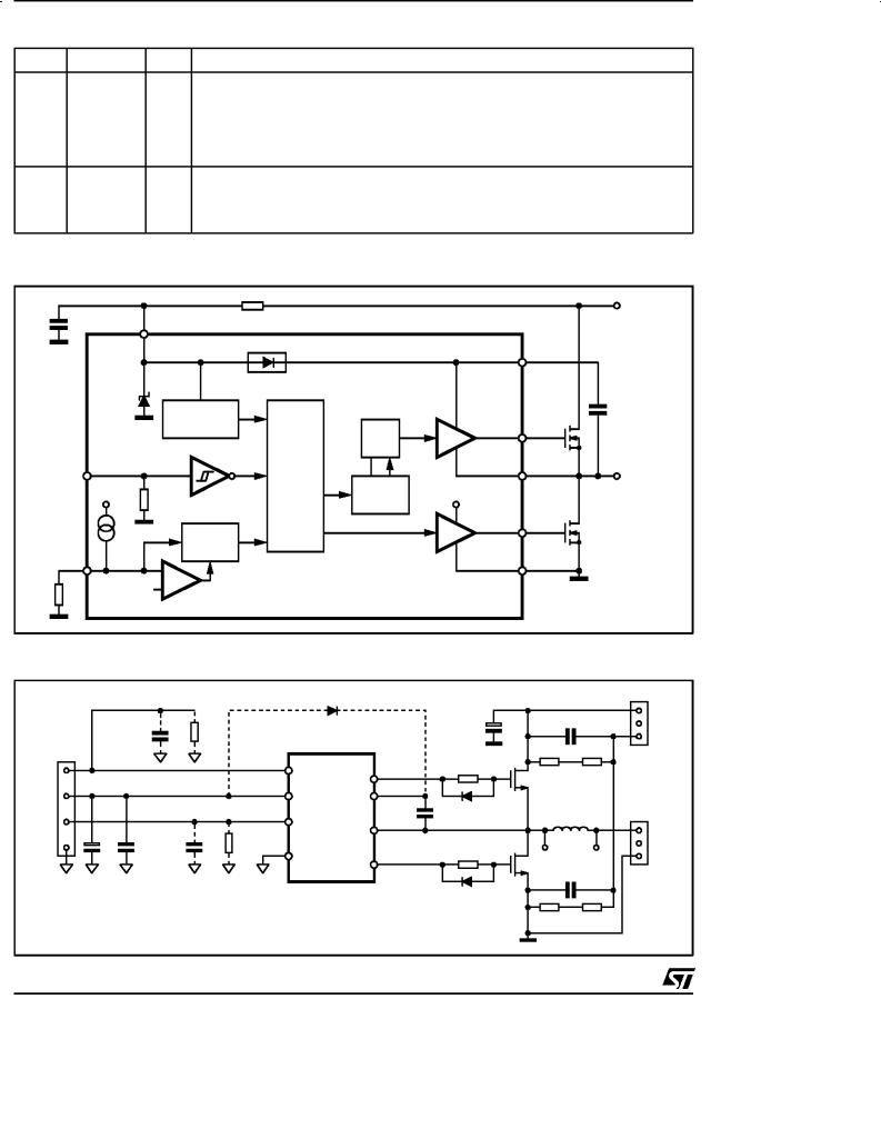
The L6384 (Internal diagram in fig. 1) is a half bridge driver with externally adjustable dead-time and shut down function. To disable the driver, the control pin (DT/SD at pin3) must be pulled down below 0.5V. The dead time can be set from 0.5μs to 2.7μs by a simple resistor between pin3 and ground.
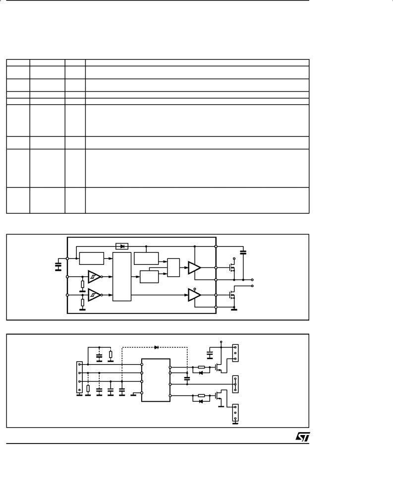
Available in Minidip and SO8 packages, this driver can be used in motor controls, resonant converters and lighting applications. In fig. 2 the schematic diagram of the evaluation circuit and the layout of the test PCB are shown.
L6384 PIN DESCRIPTION
N. |
Name |
Type |
Function |
1 |
IN(*) |
I |
Logic Input: it is in phase with HVG and in opposition of phase with LVG. It is |
|
|
|
compatible to Vcc voltage. |
2 |
VCC |
I |
Supply input voltage: there is an internal clamp [Typ. 15.6V] |
|
|
|
There is also an UVLO feature ( Typ. Vccth1 = 12V, Vccth2 = 10V). |
3 |
DT/SD |
I |
High impedence pin with two functionalities. When pulled to a voltage lower than Vdt |
|
|
|
[Typ.0.5V] the device is shut down. A voltage higher than Vdt sets the dead time |
|
|
|
between high side and low side gate driver. The dead time value can be set forcing a |
|
|
|
certain voltage level on the pin or connecting a resistor between pin 3 and ground. |
|
|
|
Care must be taken to avoid spikes on pin 3 that can cause undesired shut down of |
|
|
|
the IC. For this reason the connection of the components between pin 3 and ground |
|
|
|
has to be as short as possible. This pin can not be let floating for the same reason. |
|
|
|
The pin has not to be pulled through a low impedence to Vcc, because of the drop on |
|
|
|
the corrent source that feeds Rdt. The operative range is: Vdt ... 270K Idt, that allows |
|
|
|
a dt range of 0.4 - 3.1μs. |
4 |
GND |
|
Ground |
5 |
LVG |
O |
Low side driver output: the output stage can deliver 400mA source and 650mA sink |
|
|
|
[Typ. Values]. |
|
|
|
The circuit guarantees 0.3V max on the pin (@Isink = 10mA) with Vcc > 3V and lower |
|
|
|
than the turn on threshold. This allows to omit the bleeder resistor connected between |
|
|
|
the gate and the the source of the external mosfet normally used to hold the pin low; |
|
|
|
the gate driver ensures low impedence also in SD conditions. |
6 |
Vout |
O |
Upper driver floating reference: layout care has to be taken to avoid undervoltage |
|
|
|
spikes on this pin |
June 2002 |
1/17 |
AN994 APPLICATION NOTE
L6384 PIN DESCRIPTION (continued)
N. |
Name |
Type |
Function |
7 |
HVG |
O |
High side driver output:the output stage can deliver 400mA source and 650mA sink |
|
|
|
[Typ. Values]. |
|
|
|
The circuit guarantees 0.3V max between this pin and Vout (@Isink = 10mA) with Vcc > |
|
|
|
3V and lower than the turn on threshold. This allows to omit the bleeder resistor |
|
|
|
connected between the gate and the the source of the external mosfet normally used |
|
|
|
to hold the pin low; the gate driver ensures low impedence also in SD conditions. |
8 |
Vboot |
|
Bootstrap Supply Voltage: it is the upper driver floating supply. The bootstrap |
|
|
|
capacitor connected between this pin and pin 6 can be fed by an internal structure |
named ºbootstrap driverº (a patented structure). This structure can replace the external bootstrap diode.
(*) The pull-down internal resistor is typically some hundreds Kohm.
Figure 1. L6384 Internal Block Diagram.
|
|
|
|
|
|
H.V. |
|
|
VCC |
|
|
|
|
|
|
|
2 |
|
8 |
VBOOT |
|
|
|
|
|
||
|
|
|
BOOTSTRAP DRIVER |
|
|
|
|
|
|
UV |
|
HVG |
CBOOT |
|
|
|
DETECTION |
|
DRIVER |
HVG |
|
|
|
|
|
||
|
|
|
R S |
|
7 |
|
IN |
1 |
|
LOGIC |
|
|
OUT |
|
|
|
6 |
LOAD |
||
|
|
|
LEVEL |
|
|
|
|
VCC |
|
|
VCC |
|
|
|
|
SHIFTER |
|
|||
|
|
|
|
|
||
|
|
Idt |
|
|
5 |
LVG |
|
|
DEAD |
|
|
|
|
|
|
|
|
|
|
|
DT/SD |
|
|
TIME |
LSG |
4 |
GND |
|
|
|
DRIVER |
|||
|
|
|
|
|
|
|
3
Vthi
D97IN518A
Figure 2. L6384 Schematic diagram of the evaluation circuit.
CN3
D1
|
|
|
|
|
|
C5 |
|
C6 |
|
|
|
|
|
|
|
|
|
|
|
CN1 |
|
IN |
|
|
|
|
|
|
|
|
|
1 |
HVG |
|
R2 |
|
|
|
|
|
|
|
|
R4 |
|
R5 |
|||
|
|
VCC |
|
7 |
|
|
|
|
|
|
|
2 |
VBOOT |
|
|
Q1 |
|
|
|
|
|
|
8 |
|
D2 |
|
|
||
|
|
DT/DS |
L6384 |
|
C4 |
|
|
CN2 |
|
|
|
|
|
|
L1 |
||||
|
|
|
3 |
6 |
|
|
|
|
|
|
|
|
|
|
|
|
|
|
|
C1 |
C2 |
GND |
|
OUT |
|
|
|
|
|
4 |
|
|
R3 |
W1 |
|
W2 |
|||
|
|
|
5 |
|
|
||||
|
|
|
|
|
|
|
C7 |
|
|
|
|
|
|
LVG |
|
|
Q2 |
|
|
|
|
|
|
|
|
D3 |
|
|
|
|
|
|
|
|
|
|
|
|
|
|
|
|
|
|
|
|
R7 |
|
R6 |
|
|
D98IN829 |
|
|
|
|
|
|
|
2/17

AN994 APPLICATION NOTE
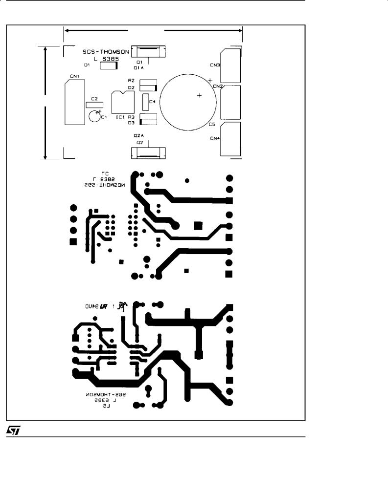
Figure 2a. L6384 - PCB and component layout of the fig. 2.
94mm
50mm |
Silk |
Comp.
Layer
Back
Layer
3/17
AN994 APPLICATION NOTE
The L6385 (Internal diagram in fig. 3) is a high and low side configurable driver. In fact, it is possible to control two separate inputs, thus the outputs can be switched independently. This device is provided with undervoltage detection in both low voltage side and high voltage bootstrapped supply. Delivered in 8pin packages, this driver has been especially designed for power supplies and motion control application. Fig. 4 shows the schematic diagram of the evaluation circuit and the layout of the relevant PCB.
L6385 PIN DESCRIPTION
N. |
Name |
Type |
Function |
1 |
LIN (*) |
I |
Low Side Driver Logic Input: it is compatible to Vcc voltage. |
|
|
|
[Vil Max = 1.5V, Vih Min = 3.6V] |
2 |
HIN (*) |
I |
High Side Driver Logic Input: it is compatible to Vcc voltage. |
3 |
VCC |
|
[Vil Max = 1.5V, Vih Min = 3.6V] |
I |
Supply input voltage with UVLO ( Typ. Vccth1 = 9.6V, Vccth2 = 8.3V). |
||
4 |
GND |
|
Ground |
5 |
LVG |
O |
Low Side Driver Output: the output stage can deliver 400mA source and 650mA sink |
|
|
|
[Typ. Values]. |
|
|
|
The circuit guarantees 0.3V max on the pin (@Isink = 10mA) with Vcc > 3V and lower |
|
|
|
than the turn on threshold. This allows to omit the bleeder resistor connected between |
|
|
|
the gate and the the source of the external mosfet normally used to hold the pin low. |
6 |
Vout |
O |
Upper Driver Floating Reference: layout care has to be taken to avoid undervoltage |
|
|
|
spikes on this pin. |
7 |
HVG |
O |
High Side Driver Output: the output stage can deliver 400mA source and 650mA sink |
|
|
|
[Typ. Values]. |
|
|
|
The circuit guarantees 0.3V max between this pin and Vout (@ Isink = 10mA) with Vcc > |
|
|
|
3V and lower than the turn on threshold. This allows to omit the bleeder resistor |
|
|
|
connected between the gate and the the source of the external mosfet normally used |
|
|
|
to hold the pin low. |
8 |
Vboot |
|
Bootstrap Supply Voltage:it is the upper driver floating supply [with UVLO: typ. VBSth1 |
|
|
|
= 9.5V, VBSth2 = 8.2V]. The bootstrap capacitor connected between this pin and pin 6 |
|
|
|
can be fed by an internal structure named ºbootstrap driverº (a patented structure). |
|
|
|
This structure can replace the external bootstrap diode. |
(*) The pull-down internal resistor is typically some hundreds Kohm.
Figure 3. L6385 Internal Block Diagram.
|
|
BOOTSTRAP DRIVER |
|
8 |
Vboot |
|
|
|
|
|
|
||
VCC 3 |
|
|
|
|
|
Cboot |
UV |
|
UV |
|
HVG |
H.V. |
|
|
|
|
|
|||
|
DETECTION |
|
DETECTION |
R |
|
|
|
|
DRIVER |
HVG |
|||
|
|
|
|
|
||
|
|
|
|
R |
|
|
|
|
|
|
7 |
|
|
2 |
|
|
|
S |
|
|
|
LOGIC |
LEVEL |
|
OUT |
||
HIN |
|
|
|
|||
|
SHIFTER |
|
|
|||
|
|
|
|
6 |
|
|
|
|
|
|
|
TO LOAD |
|
|
|
|
|
|
VCC |
|
1 |
|
|
|
|
5 |
LVG |
LIN |
|
|
|
|
|
|
|
|
|
|
LVG |
4 |
GND |
|
|
|
|
DRIVER |
||
D97IN514B
Figure 4. L6385 Schematic diagram of the evaluation circuit.
+HV
CN3
|
|
D1 |
|
|
|
|
|
|
|
|
|
C5 |
|
CN1 |
|
|
|
|
|
|
LIN |
1 |
|
HVG |
|
R2 |
|
|
7 |
|
|
|||
HIN |
|
VBOOT |
|
|
|
|
2 |
8 |
|
Q1 |
CN2 |
||
|
|
|
||||
VCC |
|
L6385 |
|
C4 |
D2 |
|
3 |
|
|
|
|||
|
|
6 |
VOUT |
|
|
|
C1 C2 GND |
|
|
|
|
|
|
4 |
|
|
|
R3 |
|
|
|
5 |
|
|
|
||
|
|
LVG |
|
|
|
|
|
|
|
|
Q2 |
CN4 |
|
|
|
|
|
|
||
|
|
|
|
|
D3 |
|
|
|
|
|
D98IN830 |
|
|
4/17
AN994 APPLICATION NOTE
Figure 5a. L6385 - PCB and component layout of the fig. 5.
80mm
50mm |
Silk |
|
Comp.
Layer
Back
Layer
5/17
AN994 APPLICATION NOTE
L6386 (Internal diagram in fig. 5). Configurable driver, the L6386 is based on the L6385 structure with added functions. This device is available in DIP14 or SO14.
The added Shutdown function (active low) and the Current Sense Comparator (0.5V threshold) with Diagnostic Output, make this device particularly suitable for motion control with cycle-by-cycle current feedback. DIAG and CIN pins can be used to stop the device (e.g. acting on SD pin). Fig. 6 shows the schematic diagram of the evaluation circuit and the layout of the relevant PCB.
L6386 PIN DESCRIPTION
N. |
Name |
Type |
Function |
1 |
LIN (*) |
I |
Lower Driver Logic Input: it is compatible to Vcc voltage. [Vil Max = 1.5V, Vih Min = 3.6V] |
2 |
SD (*) |
I |
Shut Down Logic Input: it is compatible to Vcc voltage. If it has to be pulled up the |
|
|
|
suggested resistor value is 5-10Kohm. [Vil Max = 1.5V, Vih Min = 3.6V] |
3 |
HIN (*) |
I |
Low Side Driver Logic Input: it is compatible to VCC voltage. [Vil Max = 1.5V, Vih Min = 3.6V] |
4 |
VCC |
I |
Low Side Driver Logic Input: it is compatible to Vcc voltage.[Vil Max = 1.5V, Vih Min = 3.6V] |
5 |
DIAG |
O |
Diagnostic Output: Open Drain |
6 |
CIN |
I |
Comparator Input |
7 |
SGND |
|
Ground reference for logic signals |
8 |
PGND |
|
Power Ground reference for the Low Voltage Gate Driver |
9 |
LVG |
O |
Low Side Driver Output: Low side driver output: the output stage can deliver 400mA |
|
|
|
source and 650mA sink [Typ. Values]. |
|
|
|
The circuit guarantees 0.3V max on the pin (@ Isink = 10mA) with VCC > 3V and lower |
|
|
|
than the turn on threshold. This allows to omit the bleeder resistor connected between |
|
|
|
the gate and the the source of the external mosfet normally used to hold the pin low; |
|
|
|
the gate driver ensures low impedence also in SD conditions. |
10, 11 |
N.C. |
|
Not Connected |
12 |
Vout |
O |
Upper Driver Floating Driver: layout care has to be taken to avoid undervoltage spikes |
|
|
|
on this pin |
13 |
HVG |
O |
High Side Driver Output: High side driver output:the output stage can deliver 400mA |
|
|
|
ource and 650mA sink [Typ. |
|
|
|
Values] The circuit guarantees 0.3V max between this pin and Vout (@ Isink = 10mA) |
|
|
|
with VCC > 3V and lower than the turn on threshold. This allows to omit the bleeder |
|
|
|
resistor connected between the gate and the the source of the external mosfet |
|
|
|
normally used to hold the pin low; the gate driver ensures low impedence also in SD |
|
|
|
conditions. |
14 |
Vboot |
|
Bootstrapped Supply Voltage: Bootstrap supply voltage: it is the upper driver floating |
|
|
|
supply [with UVLO: Typ. VBth1 = 11.9V, VBth2 = 9.9V]. |
|
|
|
The bootstrap capacitor connected between this pin and pin 6 can be fed by an |
|
|
|
internal structure named ºbootstrap driverº (a patented structure). This structure can |
|
|
|
replace the external bootstrap diode. |
(*) The pull-down internal resistor is typically some hundreds Kohm.
6/17
 Loading...