

Page 1

AN994
APPLICATION NOTE
L6384, L6385, L6386 & L6387
APPLICATIONGUIDE
by F. Sandrini, U. Moriconi
The ST L638X is a versatilehigh voltage gate driverfamily.
Realised in BCD Off-line technology, these devices are able to operate with high voltage rails up to
600V. The Gate Drivers provide all the functions and current capability necessary for high side and
low side Power MOS and IGBT.
L6384-5-6-7are High VoltageDrivers for High and Low Side. Thesedevices can be used in all the applications where high voltage shifted control is necessary.These devices have a fairly high driver current
capability and they are also providedwith an internal patentedcircuitry which replaces the externalbootstrap diode. This feature is achieved by means of a high voltage DMOS, synchronouslydriven with the
low side gate driver.
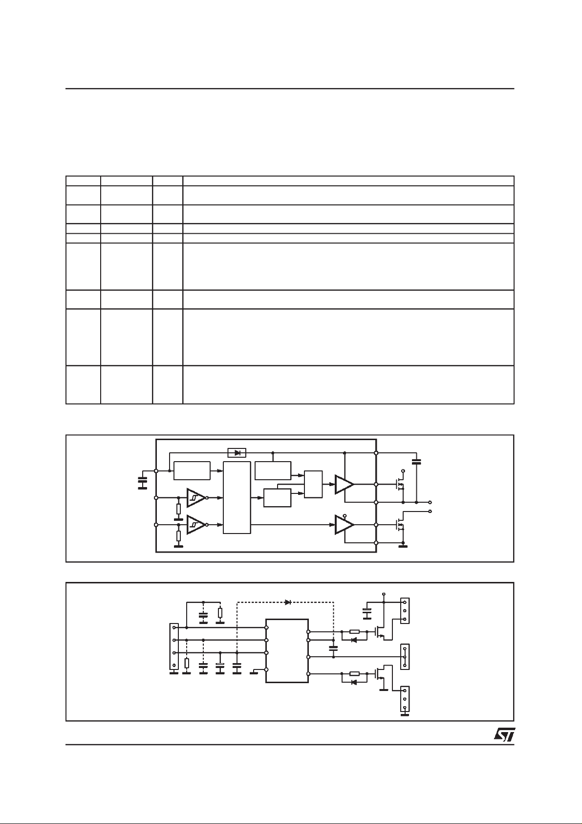
The L6384 (Internal diagram in fig. 1) is a half bridge driver with externally adjustable dead-time and
shut down function. To disable the driver, the control pin (DT/SD at pin3) must be pulled down below
0.5V. The dead time can be set from 0.5µs to 2.7µs by a simpleresistor between pin3 and ground.
Available in Minidip and SO8 packages, this driver can be used in motor controls, resonant converters
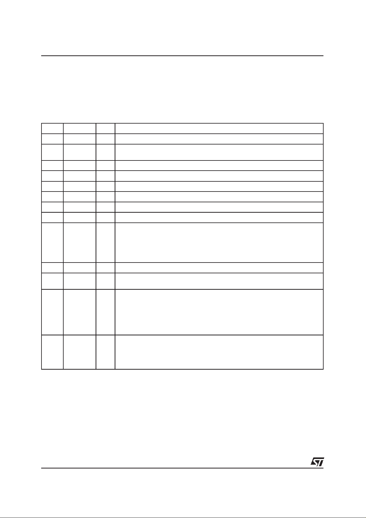
and lighting applications. In fig. 2 the schematic diagram of the evaluation circuit and the layout of the
test PCB are shown.
L6384 PIN DESCRIPTION
N. Name Type Function
1 IN(*) I Logic Input: it is in phasewith HVG and in opposition of phase with LVG. It is
2V
3 DT/SD I High impedence pin with two functionalities. When pulled to a voltage lower thanV
4 GND Ground
5 LVG O Low side driver output: the output stage can deliver 400mA source and 650mA sink
6 Vout O Upperdriver floating reference: layout care has to be taken to avoid undervoltage
CC
compatible to Vcc voltage.
I Supply input voltage: there is an internal clamp [Typ. 15.6V]
There is also an UVLO feature ( Typ. Vcc
[Typ.0.5V] the device is shut down. A voltage higher than Vdtsets the dead time
between high side and low side gate driver. The dead time value can be set forcing a
certain voltage level on the pin or connectinga resistorbetween pin 3 and ground.
Care must be taken toavoid spikes on pin 3 that can cause undesired shut down of
the IC. For this reason the connection of the components between pin 3 and ground
has to beas shortas possible. This pin can not be letfloating forthe same reason.
The pin has not to be pulled through a low impedence to Vcc, because of the drop on
the corrent source that feeds Rdt. The operativerange is:V
a dt range of 0.4 - 3.1µs.
[Typ. Values].
The circuit guarantees 0.3V max on the pin(@I
than the turn on threshold.This allows to omit the bleeder resistor connected between
the gate and the the source of the external mosfet normallyused to hold the pin low;
the gate driver ensures low impedence also in SD conditions.
spikes on this pin
= 12V, Vcc
th1
= 10V).
th2
... 270K ⋅ Idt, that allows
dt
= 10mA) with Vcc> 3V and lower
sink
dt
June 2002
1/17
Page 2

AN994 APPLICATIONNOTE
L6384 PIN DESCRIPTION(continued)
N. Name Type Function
7 HVG O Highside driver output:the output stage can deliver 400mA source and 650mA sink
8V
(*) The pull-down internal resistor is typically some hundreds Kohm.
boot
Figure 1. L6384 Internal Block Diagram.
V
CC
2
[Typ. Values].
The circuit guarantees 0.3V max between this pinand Vout (@I
= 10mA) with Vcc>
sink
3V and lower than the turn on threshold.This allows to omit the bleeder resistor
connected betweenthe gate and the the sourceof the external mosfet normally used
to hold the pin low; the gate driver ensures low impedence also in SD conditions.
Bootstrap Supply Voltage: it is the upper driver floatingsupply. The bootstrap
capacitor connected between this pin and pin 6 can be fed by an internal structure
named ”bootstrap driver” (a patentedstructure). This structure can replace the
external bootstrap diode.
V
8
BOOT
BOOTSTRAP DRIVER
H.V.
UV
DETECTION
RS
DT/SD
1
IN
V
CC
Idt
DEAD
TIME
3
Vthi
LOGIC
LEVEL
SHIFTER
LSG
DRIVER
Figure 2. L6384 Schematicdiagramof the evaluationcircuit.
D1
CN1
V
DT/DS
GNDC2C1
IN
1
CC
2
L6384
3
4
HVG
7
VBOOT
8
6
OUT
5
LVG C7
C4
V
CC
HVG
DRIVER
C5
R2
D2
R3
D3
7
6
5
4
Q1
Q2
HVG
OUT
LVG
GND
D97IN518A
C6
R4 R5
L1
W1 W2
C
BOOT
LOAD
CN3
CN2
2/17
R7 R6
D98IN829
Page 3

Figure 2a. L6384 - PCB and componentlayoutof the fig. 2.
94mm
AN994 APPLICATIONNOTE
50mm
Silk
Comp.
Layer
Back
Layer
3/17
Page 4
AN994 APPLICATIONNOTE
The L6385 (Internal diagram in fig. 3) is a high and low side configurable driver. In fact, it is possible to
control two separate inputs, thus the outputs can be switched independently. This device is provided
with undervoltagedetection in both low voltage side and high voltage bootstrapped supply. Delivered in
8pin packages, this driver has been especiallydesigned for power supplies and motion control application. Fig. 4 shows the schematicdiagram of the evaluationcircuitand the layoutof the relevantPCB.
L6385 PIN DESCRIPTION
N. Name Type Function
1 LIN (*) I Low Side Driver Logic Input: it is compatible to Vcc voltage.
2 HIN (*) I High Side Driver Logic Input: it is compatible to Vcc voltage.
3V
CC
4 GND Ground
5 LVG O Low Side Driver Output: the output stage can deliver 400mA source and 650mAsink
6 Vout O Upper Driver Floating Reference: layout care has to be taken to avoid undervoltage
7 HVG O High Side Driver Output: the output stage can deliver 400mA source and 650mA sink
8 Vboot BootstrapSupply Voltage:it is the upper driver floating supply [with UVLO: typ. V
(*) The pull-down internal resistor is typically some hundreds Kohm.
Figure 3. L6385 Internal Block Diagram.
[V
= 1.5V, V
il Max
[V
= 1.5V, V
il Max
I Supply input voltage with UVLO ( Typ. V
ih Min
ih Min
= 3.6V]
= 3.6V]
ccth1
= 9.6V, V
ccth2
= 8.3V).
[Typ.Values].
Thecircuit guarantees 0.3V max on the pin (@I
= 10mA) with Vcc> 3V and lower
sink
thanthe turn on threshold. This allows to omit the bleeder resistor connected between
thegate and the the source of the external mosfet normally used to hold the pin low.
spikes on this pin.
[Typ.Values].
Thecircuit guarantees 0.3V max between this pin and V
out
(@ I
= 10mA) with Vcc>
sink
3Vand lower than the turn on threshold. This allows to omit the bleeder resistor
connected between the gate and the the source of the external mosfet normallyused
to hold the pin low.
= 9.5V, V
= 8.2V]. The bootstrapcapacitor connected between this pin and pin 6
BSth2
canbe fed by an internal structure named ”bootstrap driver” (a patented structure).
Thisstructure can replace the external bootstrap diode.
BSth1
BOOTSTRAP DRIVER
V
CC
3
HIN
LIN
2
1
UV
DETECTION
LOGIC
UV
DETECTION
LEVEL
SHIFTER
R
R
S
LVG
DRIVER
Figure 4. L6385 Schematicdiagramof the evaluationcircuit.
D1
CN1
LIN
1
HIN
2
L6385
V
CC
3
GNDC2C1
4
HVG
7
VBOOT
8
6
VOUT
5
LVG
V
CC
C4
D98IN830
HVG
DRIVER
D97IN514B
C5
R2
D2
R3
D3
8
Vboot
Cboot
H.V.
HVG
7
OUT
6
LVG
5
GND
4
+HV
Q1
Q2
TO LOAD
CN3
CN2
CN4
4/17
Page 5

Figure 5a. L6385 - PCB and componentlayoutof the fig. 5.
80mm
AN994 APPLICATIONNOTE
50mm
Silk
Comp.
Layer
Back
Layer
5/17
Page 6
AN994 APPLICATIONNOTE
L6386 (Internal diagram in fig. 5). Configurable driver, the L6386 is based on the L6385 structure with
added functions.Thisdevice is availablein DIP14or SO14.
The added Shutdown function (active low) and the Current Sense Comparator (0.5V threshold) with Diagnostic Output, make this device particularly suitable for motion control with cycle-by-cycle current
feedback.DIAG and CIN pins can be used to stop the device (e.g. acting on SD pin). Fig. 6 shows the
schematic diagramof theevaluationcircuit and the layout of therelevantPCB.
L6386 PIN DESCRIPTION
N. Name Type Function
1 LIN (*) I Lower Driver Logic Input: it is compatible to Vcc voltage. [V
2 SD (*) I Shut Down Logic Input: it is compatible to Vcc voltage. If it has to be pulled up the
suggested resistorvalue is 5-10Kohm. [V
3 HIN (*) I Low SideDriverLogic Input:it is compatibletoV
4V
CC
I Low SideDriverLogic Input:it is compatibletoVccvoltage.[V
il Max
= 1.5V, V
voltage.[V
CC
ih Min
5 DIAG O Diagnostic Output: Open Drain
6 CIN I Comparator Input
7 SGND Ground reference for logic signals
8 PGND Power Ground reference for the Low Voltage Gate Driver
9 LVG O Low Side Driver Output: Low side driver output: the outputstage can deliver 400mA
source and 650mA sink [Typ. Values].
The circuit guarantees 0.3V max on the pin(@ I
= 10mA) with VCC> 3V and lower
sink
than the turn on threshold.This allows to omit the bleeder resistor connected between
the gate and the the source of the external mosfet normallyused to hold the pin low;
the gate driver ensures low impedence also in SD conditions.
10, 11 N.C. NotConnected
il Max
= 3.6V]
il Max
ilMax
= 1.5V, V
= 1.5V,V
= 1.5V,V
ihMin
ih Min
ihMin
= 3.6V]
= 3.6V]
= 3.6V]
12 V
out
O Upper Driver Floating Driver: layout care has to be taken to avoid undervoltage spikes
on this pin
13 HVG O High Side Driver Output: High side driver output:the output stage can deliver 400mA
ource and 650mA sink [Typ.
Values] The circuit guarantees 0.3V max between this pin and Vout (@ I
with V
> 3V and lower than the turnon threshold. This allows to omit the bleeder
CC
sink
resistor connectedbetween the gate and the the source of the external mosfet
normally used to hold the pin low; the gate driver ensures low impedence also in SD
conditions.
14 Vboot Bootstrapped Supply Voltage: Bootstrap supply voltage: it is the upper driver floating
supply [with UVLO: Typ. V
= 11.9V, V
Bth1
Bth2
= 9.9V].
The bootstrap capacitor connected between thispin and pin 6 can be fed by an
internal structure named ”bootstrap driver” (a patented structure). This structure can
replace theexternal bootstrap diode.
(*) The pull-down internal resistor is typically some hundreds Kohm.
= 10mA)
6/17
Page 7

Figure 5. L6386 Internal Block Diagram.
AN994 APPLICATIONNOTE
BOOTSTRAP DRIVER
V
CC
HIN
SD
LIN
SGND
UV
DETECTION
4
3
2
1
7 6
LOGIC
UV
DETECTION
LEVEL
SHIFTER
VREF
R
R
S
-
+
LVG
DRIVER
Figure 6. L6386 Schematicdiagramof the evaluationcircuit.
DRIVER
V
CC
D97IN520D
HVG
Vboot
14
HVG
13
OUT
12
LVG
9
PGND
8
DIAG
5
CIN
H.V.
C
BOOT
TO LOAD
CN1
+HV
D1
CN3
C5
C4
R2
D2
R3
D3
CN2
CN4
GND
R1
JP1
C7
LIN
HIN
V
SD
DIAG
CIN
SGND
HVG
1
3
CC
4
2
L6386
5
6
7
13
14
12
8
9
VBOOT
OUT
PGND
LVG
R7
C2C1
C6 R4 R5 R6
D98IN831A
7/17
Page 8

AN994 APPLICATIONNOTE
Figure 6a. L6386 - PCB and componentlayoutof the fig. 6.
60mm
50mm
Silk
Comp.
Layer
8/17
Back
Layer
Page 9

AN994 APPLICATIONNOTE
L6387 (internal diagram fig.7) is based on L6385 structure. It has two separate inputs, but there is also
an interlockingfunction to avoid undesired simultaneous turn on of both Power Switches (see Truth Table). The Vcc turn on and turn off thresholds have been lowered to 6V and 5.5V(Typ.). There is no
UVLO on the upper driving section.
L6387 PIN DESCRIPTION
N. Name Type Function
1 LIN (*) I Low Side Driver Logic Input: it is compatible to Vcc voltage.
2 HIN (*) I High Side Driver Logic Input: it is compatible to Vcc voltage.
3V
CC
4 GND Ground
5 LVG O Low Side Driver Output: the output stage can deliver 400mA source and 650mAsink
6 Vout O Upper Driver Floating Reference: layout care has to be taken to avoid undervoltage
7 HVG O High Side Driver Output: the output stage can deliver 400mA source and 650mA sink
8 Vboot BootstrapSupply Voltage:it is the upper driver floating supply . The bootstrap
(*) The pull-down internal resistor is typically some hundreds Kohm.
[V
= 1.5V, V
il Max
= 1.5V, V
[V
il Max
I Supply input voltage [with very low UVLO: V
ih Min
ih Min
= 3.6V]
= 3.6V]
ccth1
=6V&V
= 5.5V (typ.).
ccth2
[Typ.Values].
Thecircuit guarantees 0.3V max on the pin (@I
= 10mA) with Vcc> 3V and lower
sink
thanthe turn on threshold. This allows to omit the bleeder resistor connected between
thegate and the the source of the external mosfet normally used to hold the pin low.
spikes on this pin.
[Typ.Values].
Thecircuit guarantees 0.3V max between this pin and V
out
(@ I
= 10mA) with Vcc>
sink
3Vand lower than the turn on threshold. This allows to omit the bleeder resistor
connected between the gate and the the source of the external mosfet normallyused
to hold the pin low.
capacitor connected between this pin and pin 6 can be fed by an internal structure
named”bootstrap driver” (a patented structure). This structure can replace the
externalbootstrap diode.
Figure 7. L6387 Internal Block Diagram.
BOOTSTRAPDRIVER
V
3
HIN
LIN
CC
2
1
UV
DETECTION
LOGIC
L6387: TRUTH TABLE
INPUT HIN 0 0 1 1
OUTPUT HVG 0 0 1 0
HVG
DRIVER
R
LEVEL
SHIFTER
S
LVG
DRIVER
V
CC
D00IN1135
LIN 0 1 0 1
LVG 0 1 0 0
8
Vboot
H.V.
HVG
7
OUT
6
LVG
5
GND
4
Cboot
TO LOAD
9/17
Page 10

AN994 APPLICATIONNOTE
BOOTSTRAPDRIVER
A bootstrapcircuitry is neededto supply the high voltage section. This functionis normally accomplished
by a high voltage fast recovery diode (fig. 8a). In the L6384-5-6-7 a patented integrated structure replaces the external diode. It is realized by a high voltage DMOS, driven synchronouslywith the low side
driver (LVG), with in series a diode, as shownin fig.8b
An internal charge pump(fig. 8b) provides the DMOS driving voltage .
The diode connectedin series to the DMOS has been added to avoidundesirableturn on of it.
C
To choose the proper C
pacitor C
selectionand charging
BOOT
is related to the MOStotal gatecharge :
EXT
BOOT
The ratio between the capacitorsC
:
value the external MOS can be seen as an equivalent capacitor. This ca-
Q
gate
=
C
EXT
V
gate
EXT
andC
isproportionalto the cyclical voltage loss .
BOOT
It has to be:
C
>>>C
BOOT
e.g.: if Q
is30nC and V
gate
gate
is 10V,C
is 3nF. With C
EXT
If HVG has to be supplied for a long time, the C
BOOT
EXT
= 100nF the drop wouldbe 300mV.
BOOT
selectionhas to take into accountalso the leakage
losses.
e.g.: HVG steady state consumption is lower than 200µA (e.g. L6385 and L6386 (L6384 → 100µA)), so
if HVGT
is 5ms,C
ON
hasto supply1µCtoC
BOOT
. This charge on a 1µF capacitor means a voltage
EXT
drop of 1V.
The internal bootstrapdriver gives great advantages: the externalfast recovery diode can be avoided (it
usually has great leakagecurrent). This structure can work only if V
in the meanwhile the LVG is on. The charging time (T
charge
) of theC
is close to GND (or lower) and
OUT
is the time in which both con-
BOOT
ditions are fulfilledandit has to be longenough to chargethe capacitor.
The bootstrap driver introduces a voltage drop due to the DMOS R
(typical L6384, L6385 and
DSON
L6386 value: 125 Ohm).At low frequency this drop can be neglected.Anyway increasing the frequency
it must be taken into account.
The followingequation is useful to compute the dropon the bootstrapDMOS:
Q
gate
=
T
R
charge
dson
dson
is the on resistance of the bootstrap
where Q
gate
DMOS, and T
V
drop
= I
charge
⋅ R
dson
→ V
drop
is the gate charge of the external power MOS, R
is the charging time of the bootstrap capacitor.
charge
For example: using a power MOS with a total gate charge of 30nC the drop on the bootstrap DMOS is
about 1V, if the T
has to be considered when the voltage drop on C
V
drop
charge
is 6µs. In fact:
V
drop
=
30nC
5µs
⋅ 125Ω ≈ 0.8V
is calculated: if this drop is too high, or the
BOOT
circuit topology doesn’t allow a sufficient charging time (e.g. Fig. 13,14,15), an external diode can be
used, and thisis the reasonfor which the external diode D1 is dotted in fig 2,4 and 6.
Working at very low frequenciesthe high side driver is very long. So C
voltagecan drop because of
BOOT
of HVG steady state consumption. To avoid extremely large capacitor (> 1-2µF) an external charge
pump can be added (see fig 9 as example).Thediodes used are bot high voltage ones: they are signal
diodes becausethe high voltage drops on C1 and C2. It is mandatorythe diodes to have a low parasitic
capacitance, because C1 and C2 have to be greater than diodes capacitance. The oscillator has to
work in order to balance the high voltage side consumption, and the minimumfrequency is fixed by C1
10/17
Page 11

AN994 APPLICATIONNOTE
and C2 values (with C1,2 33pF f>250-300KHz). Moreover the oscillator has to be able to sustain the
dV/dt of the OUT pin.
Figure 8. Bootstrap Driver
D
BOOT
V
S
HVG
LVG
ab
Figure 9. External Charge Pump
IN
VCC
DT/SD
GND
1
2
3
4
8
7
L6384
6
5
V
V
BOOT
OUT
H.V.
VBOOT
HVG
OUT
LVG
C
BOOT
TO LOAD
V
V
BOOT
OUT
H.V.
LOAD
C
BOOT
TO LOAD
D99IN1056
V
S
HVG
LVG
HV
Cboot
200nF
330pF
VCC
1N4148
1N4148
C1
33pF
1N4148
1N4148
C2
33pF
HCF4069UB
Cx
11/17
Page 12

AN994 APPLICATIONNOTE
APPLICATIONIDEAS
Here below, follows a collectionof application hints that highlight the versatility and flexibility of this family of High and Low side drivers. Moreover their simplicity and compactnessmake these devices a cost
effectivesolution.
For further informationon these ICs, please refer to:
AN1263: ”Using the internal bootstrapcurrent capability of the L6384, L6385 & L6386 in driving a six
transistorinverterbridge” by D. Nolan.
AN1299:
Figure 10. L6384 µC three-phasemotor control.
”L6384,L6385, L6386 & L6387 tricks and tips”by P. Meloncelli.
+HV
7
8
6
5
4
+HV
7
8
6
5
4
+HV
7
8
6
5
4
MOTOR
WINDING
POSITION/SPEED
SENSE
SD/DT
SD/DT
SD/DT
1
2
3
2
1
3
3
2
1
CURRENT
FEEDBACK
L6384
L6384
L6384
IN1
V
S
V
DD
µC
IN2
SD
IN3
12/17
D98IN823
Page 13

Figure 11. L6384 Dimmablelamp ballast.
5
11
12
VCO
HC4046
4
V
16
15
S
-
+
Figure 12. L6384 Half Bridge Converter
1
2
L6384
BCD
”OFF-LINE”
3
FEEDBACK
AN994 APPLICATIONNOTE
+HV
HVG
8
6
OUT
5
LVG
4
D98IN824
Q17
L
Q2
C
V
OUT
EMI~
GND
4
3
DT/ST
IN OUT
1
14
1112 10 13
7
6
9
L4990
8
5
21543
L6384
BCD
”OFF-LINE”
2
AUX
SUPPLY
HVG
7
6
C
8
V
BOOT
5
LVGVCC
BOOT
OPTO
FEEDBACK
V
OUT
D99IN1063
TL431
13/17
Page 14

AN994 APPLICATIONNOTE
Figure 13. L6385 Horizontal deflection stage.
SYNC PROCESSOR
B+
CONTROL
H-OUTPUT
STAGE
HIN
LIN
3
78
HVG
2
L6385
BCD
”OFF-LINE”
1
4
V
S
6
5
V
BOOT
OUT
LVG
STP16NF06
+V
+HV
STP5NK40Z
VB+
CC
VB+
B+ STAGE
VB+
H-YOKE
H-YOKE STAGE
H-YOKE
C
S
14/17
D98IN825
BUH715
STP16NF06
C
S
H-YOKE STAGE
Page 15

Figure 14. L6385 Two switch forward converter.
EMI~
AN994 APPLICATIONNOTE
4
2
1
1112 10 13
7
6
14
9
L4990
8
5
21543
L6385
BCD
”OFF-LINE”
3
AUX
SUPPLY
7
6
8
5
LVGVCC
D98IN826A
HVG
OUT
V
BOOT
C
BOOT
OPTO
TL431
FEEDBACK
V
OUT
Figure 15. L6385 Asymmetricalhalfbridge.
V
CC
3
L6385
2
IN
1
4
”OFF-LINE”
BCD
+HV
HVG
7
OUT
6
V
BOOT
8
LVG
5
D98IN827
M
15/17
Page 16

AN994 APPLICATIONNOTE
Figure 16. L6386 H-bridge with cycle by cycle control.
HIN
SD
LIN
V
S
DIAG CIN
4
3
2
1
”OFF LINE”
5
GND
L6386
BCD
8
+HV
HVG
13
OUT
12
V
BOOT
14
LVG
9
6
VDD
TACHO
SD LINHIN
µ
M
C
V
HVG
OUT
BOOT
LVG
13
12
14
”OFF LINE”
9
6
CIN
D98IN828A
L6386
BCD
8
GND
4
3
2
1
5
DIAG
HIN
SD
LIN
16/17
Page 17

AN994 APPLICATIONNOTE
Information furnished is believed to be accurate and reliable. However, STMicroelectronics assumes no responsibility for the consequences
of use of such information nor for any infringement of patents or other rights of third parties which may result from its use. No license is
granted by implication or otherwise under any patent or patent rights of STMicroelectronics. Specification mentioned in this publication are
subject to change without notice. This publication supersedes and replaces all information previously supplied. STMicroelectronicsproducts
are not authorized for use as critical components in life support devices or systems without express written approval of STMicroelectronics.
The ST logo is a registered trademark of STMicroelectronics
2002 STMicroelectronics – Printedin Italy – All Rights Reserved
STMicroelectronics GROUP OF COMPANIES
Australia - Brazil - Canada - China - Finland -France - Germany - HongKong- India - Israel - Italy - Japan - Malaysia - Malta - Morocco -
Singapore - Spain - Sweden - Switzerland- United Kingdom - UnitedStates.
http://www.st.com
17/17
 Loading...