

Page 1

PREPARED BY: DATE
LIQUID CRYSTAL DISPLAY GROUP
Sakai Display Products Corporation
SPEC No.
FILE No.
ISSUE : Dec, 20, 2012 APPROVED BY: DATE
PAGE :
LD-K24Z07
SPECIFICATION
CUSTOMER'S APPROVAL
DATE
BY BY
MODEL No.
DEVICE SPECIFICATION FOR
DEVICE SPECIFICATION FOR
TFT-LCD Open Cell
JE400D3HC2N
PRESENTED
K.Kobayashi
Center General Manager
Technology Center
Liquid Crystal Display Business Group
Sakai Display Products Corporation
Sakai Display Products Corporation
Page 2

RECORDS OF REVISION
MODEL No. : JE400D3HC2N
SPEC No. : LD-K24Z07
SPEC No. DATE
LD-K24Z07 2012/12/20
REVISED
No.
- - - 1st ISSUE
PAGE SUMMARY NOTE
Page 3
LD-K24Z07-1
1 Application
This specification applies to the color 40.0” TFT-LCD Open Cell JE400D3HC2N.
With parts (S-Dr, G-Dr, S-PWB) to drive it.)
(
* This specification sheets are proprietary products of Sakai Display Products Corporation (“SDP”) and include
materials protected under copyright of SDP. Do not reproduce or cause any third party to reproduce them in any
form or by any means, electronic or mechanical, for any purpose, in whole or in part, without the express written
permission of SDP.
* In case of using the device for applications such as control and safety equipment for transportation (aircraft, trains,
automobiles, etc.), rescue and security equipment and various safety related equipment which require higher
reliability and safety, take into consideration that appropriate measures such as fail-safe functions and redundant
system design should be taken.
* Do not use the device for equipment that requires an extreme level of reliability, such as aerospace applications,
telecommunication equipment (trunk lines), nuclear power control equipment and medical or other equipment for
life support.
* SDP assumes no responsibility for any damage resulting from the use of the device that does not comply with the
instructions and the precautions specified in these specification.
* Contact and consult with the SDP sales representative for any questions about this device.
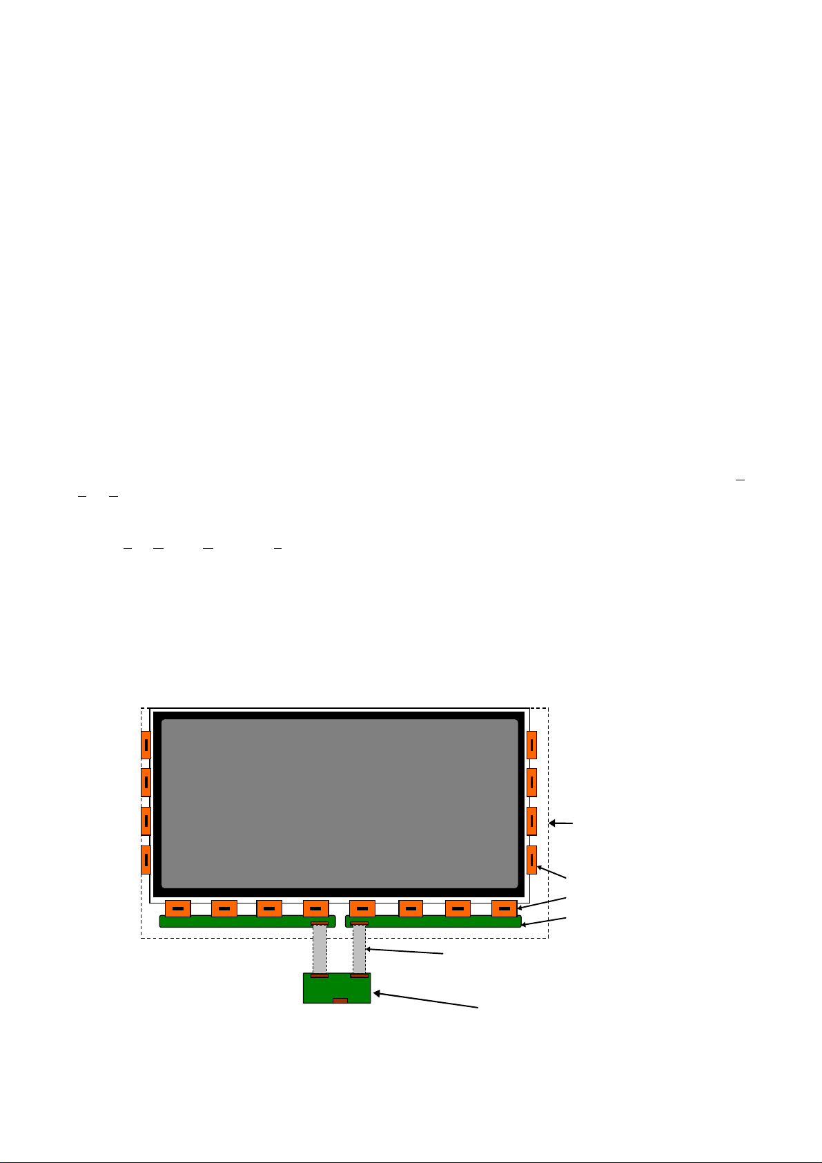
2 Overview
This Open Cell (JE400D3HC2N) is a color active matrix LCD PANEL incorporating amorphous silicon TFT (Thin
Film Transistor), Polarizers, Source-PWBs, Source-Drivers, Gate-Drivers and Control-PWB(C-PWB). The following
content can be achieved in using C-PWB (JE0DZ1C0010) that SDP specifies.
Graphics and texts can be displayed on a 1920×RGB×1080 dots panel with one billion colors by using 10bit
LVDS (Low Voltage Differential Signaling) to interface, +12V of DC supply voltages.
In order to improve the response time of LCD, This C-PWB applies the Over Shoot driving (O/S driving)
technology for the control circuit. In the O/S driving technology, signals are being applied to the Liquid Crystal
according to a pre-fixed process as an image signal of the present frame when a difference is found between image
signal of the previous frame and that of the current frame after comparing them.
With combination of this technologies, motion blur can be reduced and clearer display performance can be realized.
[Caution] You should design thermal conductive interface pad and C-PWB cover enough to radiate heat from T-CON
IC in C-PWB.
TFT LCD Panel
(1920 x RGB x 1080)
Fig.1 Overview of Open-Cell: JE400D3HC2N and C-PWB
Open Cell
Open Cell
Open CellOpen Cell
((((JE400D3HC2N
JE400D3HC2N))))
JE400D3HC2NJE400D3HC2N
Gate Driver
Source Driver
CN2
CN2
CN1
FFC (not attached)
CN3
CN1
1111
55551111
Control
Control----PW
ControlControl
PWB (JE0DZ1C0010)
PWPW
Source PWB (S-PWB)
B (JE0DZ1C0010)
B (JE0DZ1C0010)B (JE0DZ1C0010)
Page 4
Pin No.
Symbol
Function
Remark
1
GND
2
Reserved
It is required to set non
-
connection(OPEN)
3
Reserved
It is required to set non
-
connection(OPEN)
4
Reserved
It is required to set non
-
connection(OPEN)
5
Reserved
It
is required to set non
-
connection(OPEN)
6
Reserved
It is required to set non
-
connection(OPEN)
7
SELLVDS
Select LVDS data order
[Note
1,2]
Pull
down
8
Reserved
It is required to set non
-
connection(OPEN)
9
Reserved
It is required to set non
-
connection
(OPEN)
10
Reserved
It is required to set non
-
connection(OPEN)
11 GND
12
AIN0
- Aport (
-
)LVDS CH0 differential data input
13
AIN0+
Aport (+)LVDS CH0 differential data input
14
AIN1
- Aport (
-
)LVDS CH1 differential data input
15
AIN1+
Aport (+)LV
DS CH1 differential data input
16
AIN2
- Aport (
-
)LVDS CH2 differential data input
17
AIN2+
Aport (+)LVDS CH2 differential data input
18
GND
19
ACK
- Aport LVDS Clock signal(
-)
20
ACK+
Aport LVDS Clock signal(+)
21
GND
22
AIN3
- Aport (
-
)LVDS
CH3 differential data input
23
AIN3+
Aport (+)LVDS CH3 differential data input
24
AIN4
- Aport (
-
)LVDS CH4 differential data input
25
AIN4+
Aport (+)LVDS CH4 differential data input
26
GND
27
GND
28
BIN0
- Bport (
-
)LVDS CH0 differential data in
put
29
BIN0+
Bport (+)LVDS CH0 differential data input
30
BIN1
- Bport (
-
)LVDS CH1 differential data input
3 Mechanical Specifications
Parameter Specifications Unit
Display size
Active area 885.60(H) x 498.15 (V) mm
Pixel Format
Pixel pitch 0.46125 (H) x 0.46125 (V) mm
Pixel configuration R, G, B vertical stripe
Display mode Normally black
Cell Outline Dimensions[Note1] 921.18 (H) x 541.25(V) x 1.66(D) mm
Mass 1.72+0.3 kg
Surface treatment [Note2]
Underside Surface
treatment [Note2]
[Note1] Outline dimensions are shown in P20. Dimension "D" does not include the parts on S-PWB.
[Note2] With the protection film removed.
101.61 (Diagonal)
40.00 (Diagonal)
1920(H) x 1080(V)
1pixel = R + G + B dot)
(
Anti Glare
Hard coating : 2H and more
Hard coat less
4 Cell Driving Specifications
4.1 Driving interface of Control PWB SDP specifies
Parts code: JE0DZ1C0010
CN1 (Interface signals and +12V DC power supply) shown in Fig.1
Using connector : 91213-0510 (Aces Electronics Co., Ltd.)
Matching connector : FI-RE51HL, FI-RE51CL (Japan Aviation Electronics Ind., Ltd.) or
equivalent device
Matching LVDS transmitter : THC63LVD1023 or equivalent device
LD-K24Z07-2
cm
inch
pixel
Page 5
31
BIN1+
Bport (+)LVDS CH1 differential data input
32
BIN2
- Bport (
-
)LVDS CH2 differential data input
33
BIN2+
Bport (+)LVDS CH2 differentia
l data input
34
GND
35
BCK
- Bport LVDS Clock signal(
-)
36
BCK+
Bport LVDS Clock signal(+)
37
GND
38
BIN3
- Bport (
-
)LVDS CH3 differential data input
39
BIN3+
Bport (+)LVDS CH3 differential data input
40
BIN4
- Bport (
-
)LVDS CH4 differential d
ata input
41
BIN4+
Bport (+)LVDS CH4 differential data input
42
GND
43
GND
44
GND
45
GND
46
GND
47
VCC
+12V Power Supply
48
VCC
+12V Power Supply
49
VCC
+12V Power Supply
50
VCC
+12V Power Supply
51
VCC
+12V Power Supply
[Note] You should connect GND plane in Control PWB to module chassis.
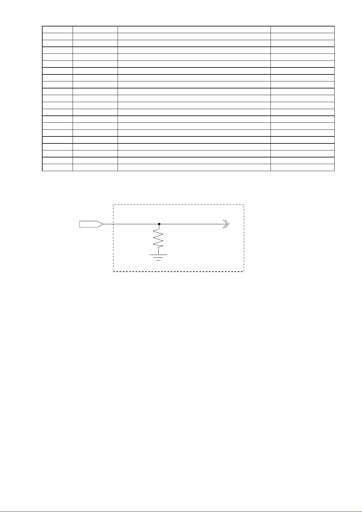
[Note 1] The equivalent circuit figure of the terminal:
Terminal
LD-K24Z07-3
4.7KΩ
Control PWB
Page 6
LD-K24Z07-4
[Note 2] LVDS Data order
SELLVDS
Data L(GND) or Open
[VESA]
TA0
TA1
TA2
TA3
TA4
TA5
TA6
TB0
TB1
TB2
TB3
TB4
TB5
TB6
TC0
TC1
TC2
TC3
TC4 NA NA
TC5 NA NA
TC6 DE(*) DE(*)
TD0
TD1
TD2
TD3
TD4
TD5
TD6
TE0
TE1
TE2
TE3
TE4
TE5
TE6
NA: Not Available
(*)Since the display position is prescribed by the rise of DE(Display Enable)signal, please do not fix DE signal
at ”High” during operation. And you should input DE signal in all LVDS port.
R0(LSB)
R1
R2
R3
R4
R5
G0(LSB)
G1
G2
G3
G4
G5
B0(LSB)
B1
B2
B3
B4
B5
R6
R7
G6
G7
B6
B7
N/A
R8
R9(MSB)
G8
G9(MSB)
B8
B9(MSB)
N/A
H(3.3V)
[JEIDA]
R4
R5
R6
R7
R8
R9(MSB)
G4
G5
G6
G7
G8
G9(MSB)
B4
B5
B6
B7
B8
B9(MSB)
R2
R3
G2
G3
B2
B3
N/A
R0(LSB)
R1
G0(LSB)
G1
B0(LSB)
B1
N/A
Page 7
SELLVDS= Low (GND) or OPEN::::VESA
ACK+,BCK+
ACK– ,BCK
AIN0+,BIN0+
AIN0–,BIN0
AIN1+,BIN1+
AIN1–,BIN1
–
–
–
G0 R5 R4 R3 R2 R1 R0 R0 R1 G0
B1 B0 G5 G4 G3 G2 G1 G1 G2 B1
AIN2+,BIN2+
AIN2–,BIN2
AIN3+,BIN3+
AIN3–,BIN3
–
–
DE
AIN4+,BIN4+
AIN4–,BIN4
–
SELLVDS= High (3.3V)::::JEIDA
ACK+,BCK+
ACK– ,BCK
AIN0+,BIN0+
AIN0–,BIN0
AIN1+,BIN1+
AIN1–,BIN1
AIN2+,BIN2+
AIN2–,BIN2
AIN3+,BIN3+
AIN3–,BIN3
AIN4+,BIN4+
AIN4
–
,BIN4
–
–
–
–
G4 R9 R8 R7 R6 R5 R4 R4 R5 G4
B5 B4 G9 G8 G7 G6 G5 G5 G6 B5
DE
–
–
DE: Display Enable, NA: Not Available (Fixed Low)
NA NA
B7 B6 G7 G6 R7 R6 R6 R7 NA NA
B9 B8 G9 G8 R9 R8 R8 R9 NA NA
NA NA
B3 B2 G3 G2 R3 R2 R2 R3 NA NA
B1 B0 G1 G0 R1 R0 R0 R1 NA NA
1 cycle
B5 B4 B3 B2 B2 B3
1 cycle
B9 B8 B7 B6 B6 B7
LD-K24Z07-5
DE
DE
Page 8

INPUT SIGNALS
GATE DRIVER
SOURCE
DRIVER
CN4
SOURCE
PWB SOURCE
PWB
INPUT SIGNALS
I2C SCL
4.2
4.2
Interface block diagram
4.24.2
SELLVDS
AIN0- AIN0+
AIN1- AIN1+
AIN2- AIN2+
AIN3- AIN3+
AIN4- AIN4+
ACK- ACK+
BIN0- BIN0+
BIN1- BIN1+
BIN2- BIN2+
BIN3- BIN3+
BIN4- BIN4+
BCK- BCK+
POWER SUPPLY
+12V DC
4.3
4.3
Display position of data
4.34.3
LCD PANEL
1920×3(RGB)×1080
GATE DRIVER
Signals &
Power Supply
Signals &
Power Supply
C-PWB
CN1
Fig.2 Interface block diagram
LD-K24Z07-6
I2C SDA
B1 G1 R1 B2 G2 R2
(1,1) (1,2)
1,1 1,2 1,3
2,1 2,2
3,1
B G R
1080,1
S-PWB S-PWB
1,1920
1080,1920
[Note] You should assemble Open-Cell for S-PWBs to be located at the downside of your TV set.
Page 9

4.4 Vcom Adjusting interface of Control PWB SDP specifies [JE0DZ1C0010]
1 pixel
For the prevention of long-time image sticking of TFT-LCD panel, be sure to adjust Vcom
flicker to be minimized on the center of display by visual or flicker meter.
.
[Note 1] Please adjust VCOM voltage at below pattern:
V0
V0
V0
V0
V512
V512
V512
V0
V0
V512
V512
V0
V0
V512
V0
V512
V0
V512
V512
V0
V512
V0
V512
V512
V0
V0
V512
1 dot
[Note 2] VCOM voltage can be adjusted through via hole (CN4). Potentiometer IC and via hole are as follows:
IC for adjusting VCOM : ISL24837A (Intersil)
Using Via Hole : 1.5mm Pitch (φ0.7mm )
Mating connector : (housing)5P-SZN,
(contact)SZN-002T-P0.7K (JST Co.,Ltd.)
Communication method
: I2C
CN4
Pin No.
symbol Function Remark
1 SCL I2C CLK Pull up:3.3V[Note3]
2 SDA I2C DATA
3 BUS_EN
4
- -
-
Pull up:3.3V[Note3]
Required to set NC
5 GND GND -
[Note3] The equivalent circuit figure of the terminal
3.3[V]
3.3[V]
2.2 [kΩ]
Terminal
Terminal
Terminal
LD-K24Z07-7
Page 10

4.5 Driving interface of S-PWB
CN1 and CN2 on the S-PWB: Input signal from C-PWB
- Using connector: 25P80B120 (ZXEC) or equivalent connector
Pin No.
CN1 on the S-PWB CN2 on the S-PWB
GND GND
1
Gate Power (L) Gate Power (L)
2
Gate Power (H) Gate Power (H)
3
Gate Start Pulse2 Gate Start Pulse 2
4
Gate Start Pulse1 Gate Start Pulse 1
5
Gate Clock Gate Clock
6
Gate Output Enable Gate Output Enable
7
Gate Scan Control Gate Scan Control
8
MPD Control 1 MPD Control 1
9
MPD Control 2
10
MPD Control 3
11
MPD Control 4
12
MPD Control 5
13
MPD Control 6
14
MPD Control 7
15
MPD Control 8
16
MPD Control 9
17
MPD Control 10
18
MPD Control 11
19
MPD Control 12
20
21 Vcom Vcom
22 Gray Level 9 (H) Gray Level 9 (H)
23 Gray Level 8 (H) Gray Level 8 (H)
24 Gray Level 7 (H) Gray Level 7 (H)
25 Gray Level 6 (H) Gray Level 6 (H)
26 Gray Level 5 (H) Gray Level 5 (H)
27 Gray Level 4 (H) Gray Level 4 (H)
28 Gray Level 3 (H) Gray Level 3 (H)
29 Gray Level 2 (H) Gray Level 2 (H)
30 Gray Level 1 (H) Gray Level 1 (H)
31 miniLVDS data(+) GND
32 miniLVDS data(-)
33 miniLVDS data(+)
34 miniLVDS data(-)
35 miniLVDS data(+)
36 miniLVDS data(-)
37 GND
38 miniLVDS clock(+)
39 miniLVDS clock(-)
40 GND
41 miniLVDS data(+)
42 miniLVDS data(-)
43 miniLVDS data(+)
44 miniLVDS data(-)
45 miniLVDS data(+) miniLVDS Scan Control
46 miniLVDS data(-)
47 Logic Circuit Power Logic Circuit Power
48 Logic Circuit Power Logic Circuit Power
MPD Control 2
MPD Control 3
MPD Control 4
MPD Control 5
MPD Control 6
MPD Control 7
MPD Control 8
MPD Control 9
MPD Control 10
MPD Control 11
MPD Control 12
GND
GND
GND
GND
GND
GND
GND
GND
GND
GND
GND
GND
miniLVDS Cascade
Control 2
miniLVDS Cascade
Control 1
LD-K24Z07-8
Page 11

49 Reserved Reserved
50 Polarity Control Polarity Control
51 Latch Strobe Latch Strobe
52 GND GND
miniLVDS Cascade
53
Control 2
54 miniLVDS Scan Control miniLVDS data(-)
miniLVDS Cascade
55
Control 1
56 GND miniLVDS data(-)
GND
57
58
59
60
61
62
63
64
65
66
67
68
69
70
71
72
73
74
75
76
77
78
79
80
GND
GND
GND
GND
GND
GND
GND
GND
GND
GND
GND
Analog circuit power Analog circuit power
Analog circuit power Analog circuit power
Gray Level 1 (L) Gray Level 1 (L)
Gray Level 2 (L) Gray Level 2 (L)
Gray Level 3 (L) Gray Level 3 (L)
Gray Level 4 (L) Gray Level 4 (L)
Gray Level 5 (L) Gray Level 5 (L)
Gray Level 6 (L) Gray Level 6 (L)
Gray Level 7 (L) Gray Level 7 (L)
Gray Level 8 (L) Gray Level 8 (L)
Gray Level 9 (L) Gray Level 9 (L)
GND GND
miniLVDS data(+)
miniLVDS data(+)
miniLVDS data(+)
miniLVDS data(-)
GND
miniLVDS clock(+)
miniLVDS clock(-)
GND
miniLVDS data(+)
miniLVDS data(-)
miniLVDS data(+)
miniLVDS data(-)
miniLVDS data(+)
miniLVDS data(-)
LD-K24Z07-9
Page 12

5 Absolute Maximum Ratings
Parameter Symbol Condition Ratings Unit Remark
Input voltage
(for Control)
12V supply voltage
(for Control)
VI
VCC
Ta=25 °C
Ta=25 °C
LD-K24Z07-10
-0.3 ~ +3.60 V [Note 1]
0 ~ + 14 V [Note 2]
Storage temperature Tstg
Operation temperature
(Ambient)
Source driver chip
surface temperature
[Note 1] Applies to the input signals to C-PWB SELLVDS, SCL, SDA.
[Note 2] Applies to the supply voltage of C-PWB.
[Note 3] Applies to the JE400D3HC2N(Open-Cell) and C-PWB
-
Humidity: 95%RH Max.(Ta < 40oC)
-
Maximum wet-bulb temperature at 39oC or less. (Ta > 40oC)
-
No condensation.
[Note 4] Recommended operating condition:chip surface temperature ≦ 115℃.
※Please take measures of the heat radiation .
Topa
Tc
-
-
-
-25 ~ +60
0 ~ +50
+115
°C
°C
℃
[Note 3]
[Note 4]
Page 13

LD-K24Z07-11
=10.8V
V2
=9.1V
ON
t4
0.9Vcc
0.1Vcc
t3
OFF
ON
OFF
Data1
t2
t5-1t5-
2
ON
2
0.9Vcc
0.1Vcc
0.1Vcc
ON
t1
t3
OFF
t8-1t8-
2
ON
6 Electrical Characteristics of input signals
Parameter Symbol Min. Typ. Max. Unit Remark
Supply voltage Vcc 11.4 12 12.6 V [Note 1]
+12V supply
voltage
Permissible input ripple voltage VRP - - 100 mV
threshold voltage
Input Low voltage VIL 0 - 0.7 V
Input High voltage VIH 2.3 3.3 3.6 V
Input leak current (Low) IIL - - 1500 µA
Input leak current (High) IIH - - 700 µA
[Note]VCM: Common mode voltage of LVDS driver.
[Note1]
Input voltage sequences Dip conditions for supply voltage
Vcc
SCL
SDA
※ Data1: ACK±, AIN0±, AIN1±, AIN2±, AIN3±, AIN4±,BCK±, BIN0±, BIN1±, BIN2±, BIN3±, BIN4±
※ Data2: SELLVDS
※ About the relation between data input and back light lighting, we recommend the above-mentioned input
Current dissipation
Inrush current I
High VTH - - 100 mV Differential input
Icc - 0.56 1.4 A [Note 2]
1 - 4.0 - A
RUSH
P-P
Vcc = +12.0V
VCM = +1.2V
Low VTL -100 - - mV
Terminal resistor RT - 100 -
Ω
Differential
50us < t1 < 20ms 9.1V < Vcc < 10.8V
20ms < t2 < 50ms td < 10ms
20ms < t3 < 50ms
0 < t4 < 1s This case is based on input voltage sequences.
1s < t
0 < t
1s < t
1s < t
6 -1
5-1
7
8-1
1s < t
0 < t
1s < t
5-2
6 -2
8-2
Vcc
V1
t7
td
t6-1
OFF
t6-
Ta=25 °C
t1=500us
[Note 4]
[Note 3]
SELLVDS
VI = 0V
SCL,SDA
VI = 3.3V
SELLVDS
input
Page 14

LD-K24Z07-12
(3V/div)
sequence. If the back light is switched on before a panel operation begins or after a panel operation stops,
the screen may not be displayed properly. But this phenomenon is not caused by change of an incoming
signal, and does not give damage to a liquid crystal display.
[Note 2] Typical current situation: 1024 gray-bar patterns. (Vcc = +12.0V)
The explanation of RGB gray scale is seen in section 8.
RGB
GS0→GS1→GS2→ ・・・・・・ →GS1023
Vcc=+12.0V
CK=74.25MHz
TH=14.8µs
[Note 3] ACK±, AIN0±, AIN1±, AIN2±, AIN3±, AIN4±, BCK±, BIN0±, BIN1±, BIN2±, BIN3±, BIN4±
[Note 4] Vcc12V inrush current waveform is as follows. (I
: t1=500us)
RUSH
Vcc
I
1
RUSH
(2A/div)
4.0A
t
1
200us/div
Page 15

7
Aport DATA
B
port DATA
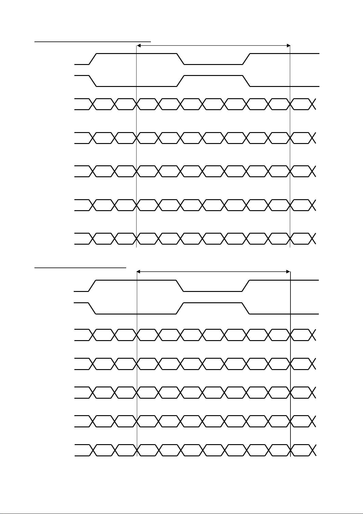
7 Timing characteristics of input signals
Timing characteristics of input signals for C
77
Timing characteristics of input signalsTiming characteristics of input signals
for C----PWB
for C for C
PWB
PWBPWB
7.1 Timing characteristics
Timing diagrams of input signal are shown in Fig.3.
Clock Frequency
Horizontal period TH
Horizontal period
Data enable
signal
(High)
Vertical period
Vertical period
(High)
1/Tc 69
1050 1100
14.2 14.8
THd
TV
960 960
1109 1125 1350
47
TVd 1080 1080 1080 line
[Note]-When vertical period is very long, flicker and etc. may occur.
-Please turn off the module after it shows the black screen.
-Please make sure that length of vertical period should become of an integral multiple of horizontal
length of period. Otherwise, the screen may not display properly.
-As for your final setting of driving timing, we will conduct operation check test at our side, please
inform your final setting.
TH
DE
(R, G, B)
1919
1
(R, G, B)
1920
Tc
2
DE
Fig3. Timing characteristics of input signal.
Typ. Parameter Symbol Min.
NTSC PAL
74.25
60 50
THd
3 1919
4 1920
1 2 1080 1079
TVd
TV
LD-K24Z07-13
Max. Unit Remark
76
MHz
1300 clock
16.1 µs
960 clock
1400
63
line
Hz
Page 16

7.2
7.2 LVDS signal characteristics
7.27.2
CLK-
Voc
CLK+
Voc
Data x-
Voc
Data x+
Voc
CLKCLK+
Data xData x+
tpd0
Vdiff=0 Vdiff=0
tpd1
tpd2
tpd3
t
CLK
Vod
Vod
tpd4
tpd5
tpd6
The item Symbol
min. typ. max. unit
Differential voltage Vod 200 400 600
Common mode voltage Voc 600 1200 1800
LVDS clock period t
Delay time, CLK rising
edge to serial bit position 0
Delay time, CLK rising
edge to serial bit position 1
Delay time, CLK rising
edge to serial bit position 2
Data
position
Delay time, CLK rising
edge to serial bit position 3
Delay time, CLK rising
edge to serial bit position 4
Delay time, CLK rising
edge to serial bit position 5
Delay time, CLK rising
edge to serial bit position 6
12.35 13.50 13.69
CLK
tpd0
tpd1
tpd2
tpd3
tpd4
tpd5
tpd6
-0.25 0 0.25
1*
t
2*
3*
4*
5*
6*
CLK
t
CLK
t
CLK
t
CLK
t
CLK
t
CLK
/7-0.25 1*
/7-0.25 2*
/7-0.25 3*
/7-0.25 4*
/7-0.25 5*
7-0.25 6*
t
CLK
t
CLK
t
CLK
t
CLK
t
CLK
t
CLK
/7 1*
/7 2*
/7 3*
/7 4*
/7 5*
/7 6*
t
t
t
t
t
t
CLK
CLK
CLK
CLK
CLK
CLK
/7+0.25
/7+0.25
/7+0.25
/7+0.25
/7+0.25
/7+0.25
LD-K24Z07-14
mV
ns
Page 17

LD-K24Z07-15
8 Input Signal, Basic Display Colors and Gray Scale of Each Color
Colors &
Gray scale
Black – 0 0 0 0 0 0 0 0 0 0 0 0 0 0 0 0 0 0 0 0 0 0 0 0 0 0 0 0 0 0
Blue – 0 0 0 0 0 0 0 0 0 0 0 0 0 0 0 0 0 0 0 0 1 1 1 1 1 1 1 1 1 1
R0 R1 R2 R3 R4 R5 R6 R7 R8 R9 G0 G1 G2 G3 G4 G5 G6 G7 G8 G9 B0 B1 B2 B3 B4 B5 B6 B7 B8 B9
Gray
Scale
Data signal
Green
Cyan – 0 0 0 0 0 0 0 0 0 0 1 1 1 1 1 1 1 1 1 1 1 1 1 1 1 1 1 1 1 1
Red – 1 1 1 1 1 1 1 1 1 1 0 0 0 0 0 0 0 0 0 0 0 0 0 0 0 0 0 0 0 0
Basic Color
Magenta – 1 1 1 1 1 1 1 1 1 1 0 0 0 0 0 0 0 0 0 0 1 1 1 1 1 1 1 1 1 1
Yellow
White
Black GS0 0 0 0 0 0 0 0 0 0 0 0 0 0 0 0 0 0 0 0 0 0 0 0 0 0 0 0 0 0 0
Darker GS2 0 1 0 0 0 0 0 0 0 0 0 0 0 0 0 0 0 0 0 0 0 0 0 0 0 0 0 0 0 0
Brighter GS1021 1 0 1 1 1 1 1 1 1 1 0 0 0 0 0 0 0 0 0 0 0 0 0 0 0 0 0 0 0 0
– 0 0 0 0 0 0 0 0 0 0 1 1 1 1 1 1 1 1 1 1 0 0 0 0 0 0 0 0 0 0
– 1 1 1 1 1 1 1 1 1 1 1 1 1 1 1 1 1 1 1 1 0 0 0 0 0 0 0 0 0 0
– 1 1 1 1 1 1 1 1 1 1 1 1 1 1 1 1 1 1 1 1 1 1 1 1 1 1 1 1 1 1
GS1 1 0 0 0 0 0 0 0 0 0 0 0 0 0 0 0 0 0 0 0 0 0 0 0 0 0 0 0 0 0
↓
↓
↓
↓
↓
↓
↓
↓
Gray Scale of Red
GS1022 0 1 1 1 1 1 1 1 1 1 0 0 0 0 0 0 0 0 0 0 0 0 0 0 0 0 0 0 0 0
Red GS1023 1 1 1 1 1 1 1 1 1 1 0 0 0 0 0 0 0 0 0 0 0 0 0 0 0 0 0 0 0 0
Black GS0 0 0 0 0 0 0 0 0 0 0 0 0 0 0 0 0 0 0 0 0 0 0 0 0 0 0 0 0 0 0
GS1 0 0 0 0 0 0 0 0 0 0 1 0 0 0 0 0 0 0 0 0 0 0 0 0 0 0 0 0 0 0
Darker GS2 0 0 0 0 0 0 0 0 0 0 0 1 0 0 0 0 0 0 0 0 0 0 0 0 0 0 0 0 0 0
Brighter GS1021 0 0 0 0 0 0 0 0 0 0 1 0 1 1 1 1 1 1 1 1 0 0 0 0 0 0 0 0 0 0
Gray Scale of Green
GS1022 0 0 0 0 0 0 0 0 0 0 0 1 1 1 1 1 1 1 1 1 0 0 0 0 0 0 0 0 0 0
↓
↓
↓
↓
↓
↓
↓
↓
Green GS1023 0 0 0 0 0 0 0 0 0 0 1 1 1 1 1 1 1 1 1 1 0 0 0 0 0 0 0 0 0 0
Black GS0 0 0 0 0 0 0 0 0 0 0 0 0 0 0 0 0 0 0 0 0 0 0 0 0 0 0 0 0 0 0
GS1 0 0 0 0 0 0 0 0 0 0 0 0 0 0 0 0 0 0 0 0 1 0 0 0 0 0 0 0 0 0
Darker GS2 0 0 0 0 0 0 0 0 0 0 0 0 0 0 0 0 0 0 0 0 0 1 0 0 0 0 0 0 0 0
Brighter GS1021 0 0 0 0 0 0 0 0 0 0 0 0 0 0 0 0 0 0 0 0 1 0 1 1 1 1 1 1 1 1
Gray Scale of Blue
GS1022 0 0 0 0 0 0 0 0 0 0 0 0 0 0 0 0 0 0 0 0 0 1 1 1 1 1 1 1 1 1
Blue GS1023 0 0 0 0 0 0 0 0 0 0 0 0 0 0 0 0 0 0 0 0 1 1 1 1 1 1 1 1 1 1
↓
↓
↓
↓
↓
↓
↓
↓
0: Low level voltage, 1: High level voltage.
Each basic color can be displayed in 1024 gray scales from 10 bits data signals. According to the combination of
total 30 bits data signals, one billion-color display can be achieved on the screen.
Page 18

9 Optical Specifications
Parameter Symbol Condition
Viewing angle
range
Horizontal
Vertical
θ
θ
θ
θ
21
22
11
12
CR>10
Ta=25°C, Vcc=12.0V, Frame rate:60Hz (typical)
Min. Typ.
Max. Unit
80 88 - Deg.
80 88 - Deg.
LD-K24Z07-16
Remark
[Note1,4]
Contrast ratio CRn
Response time
White
Red
Chromaticity
Green
Blue
Transmittance
White
τ
DRV
x
y
x
y
x
y
x
y
θ
=0 deg.
4000 5000
- 6 - ms [Note3,4,5]
Typ.-0.03
Typ.-0.03
Typ.-0.03
Typ.-0.03
Typ.-0.03
Typ.-0.03
Typ.-0.03
Typ.-0.03
0.281
0.285
0.640
0.354
0.324
0.624
0.152
0.056
6.01 %
-Optical characteristics are based on SDP standard module.
-The measurement shall be executed 60 minutes after lighting at rating.
[Note]The optical characteristics are measured using the following equipment.
Detector(EZ-CONTRAST/ Photodiode)
400mm
Center of the screen (θ=0°)
Center of the screen (θ=0°)
TFT-LCD Module
TFT-LCD Module
Fig.4-1 Measurement of viewing angle range and
Response time.
Viewing angle range: EZ-CONTRAST
Response time: Photodiode
Fig.4-2 Measurement of Contrast, Luminance,
Chromaticity.
- - [Note2,4]
Typ.+0.03
Typ.+0.03
Typ.+0.03
Typ.+0.03
Typ.+0.03
Typ.+0.03
Typ.+0.03
Typ.+0.03
-
-
-
-
-
-
-
-
Detector (SR-3A-UL1,
or equivalent one)
Field=1°
[Note4]
Page 19

LD-K24Z07-17
0%
90%
100%
time
(Relative Value)
[Note 1] Definitions of viewing angle range:
Normal line
θ
11
θ
21
θ
12
θ
22
6 o’clock direction
[Note 2] Definition of contrast ratio:
The contrast ratio is defined as the following.
Luminance (brightness) with all pixels white
Contrast Ratio
=
Luminance (brightness) with all pixels black
[Note 3] Definition of response time
The response time (τd and τr) is defined as the following figure and shall be measured by switching the input
signal for “any level of gray (0%, 25%, 50%, 75% and 100%)” and “any level of gray (0%, 25%, 50%, 75%
and 100%)”.
0%
25% 50% 75%
100%
0%
25%
50%
75%
100%
td: 25%-0%
td: 50%-0% td: 50%-25
td: 75%-0% td: 75%-25
td: 100%-0
%
tr:0%-25%
td: 100%-25
tr:0%-50% tr:0%-75% tr:0%-100%
%
%
%
tr: 25%-50
td: 75%-50
td: 100%-50
%
tr25%-75% tr: 25%-100
%
%
tr: 50%-75
td:100%-75
t*:x-y...response time from level of gray(x) to level of gray(y)
τr = Σ(tr:x-y)/10 , τd = Σ(td:x-y)/10
Bright
Dark
Bright
Photodetector
10%
Output
τd
τr
[Note 4] This shall be measured at center of the screen.
[Note 5] This value is valid when O/S driving is used at typical input time value.
%
%
tr: 50%-100
tr: 75%-100
%
%
%
Page 20

10 Shipping and Packing
del No.
10.1 Packing form
a) Open Cell quantity in 1 cell box : 20 pcs
b) Piling number of cell box : 12 pcs (Max.)
c) 1 palette size : 1390(W)×1150 (D)×1038(H) [mm]
d) Total mass of 1 palette filled with full open cells : 480 kg (Max.)
10.2 Label
a) Cell Label
This label is stuck on the protection film of front polarizer. (Please trace the Cell lot number after the film is
peeled off.)
ex) JE400D3HC2NM
Sakai Display Products
JE400D3HC2N
b) C-PWB Label & Lot No.
Mo
Barcode
2ZL00001 M
Lot No.
Lot No.: ○○○ ○○
Production year(The last figure of the Christian Era)
[Note1] L:Kameyama, Z:Sakai, N:NSEC, G:SMM, P:SMPL, X:SEMEX
How to express Lot No.
○○ ○ ○○○○○ ○
Production year(The last figure of the Christian Era)
Management code
Production Lot (A~Z,a~z)
Production month (1~9,X,Y,Z)
K0075Z 1-12Z-HD 000001
① ② ③ ④ ⑤
①Parts code
②Management code
③Production year and months:
The last two figures of the Christian
Era + Month (1~9,X,Y,Z)
④Plant code
⑤Serial No.
LD-K24Z07-18
Management code
Serial No.
Plant code [Note1]
Production month (1~9,X,Y,Z)
Page 21

c) Packing Label
This label is stuck on the packing case (cell box) and carton.
社内品番:
(4S) JE400D3HC2NM (①)
Bar code
LotNo. :
Quantity:
Bar code
ユーザ品番:
Bar code
(1T) 2013.2.1 (②)
Bar code
(Q) 20 pcs (③)
JE400D3HC2N (④)
堺ディスプレイプロダクト物流用ラベルです。
Model No. & Suffix Code
①
Lot No. (Date)
②
Quantity
③
Model No. for USER
④
LD-K24Z07-19
11 Carton storage condition.
Temperature 0°C to 40°C
Humidity 95%RH or less
Reference condition : 20°C to 35°C, 85%RH or less (summer)
: 5°C to 15°C, 85%RH or less (winter)
· the total storage time (40°C, 95%RH) : 240H or less
Sunlight Be sure to shelter a product from the direct sunlight.
Atmosphere Harmful gas, such as acid and alkali which bites electronic components and/or
wires must not be detected.
Notes Be sure to put cartons on palette or base, don’t put it on the floor, and store them
keeping off the wall. Please take care of ventilation in storehouse and around cartons,
and control temperature not to exceed the limit one of natural environment.
Storage life 1 year
Page 22

LD-K24Z07-20
I
oniz
ed air
12 Reliability
Reliability test item:
No.
1
2
3
4
5
6
7
High temperature storage test
Low temperature storage test
High temperature and high humidity
High temperature operation test
Low temperature operation test
(Cell Box with full Open Cells)
(Cell Box with full Open Cells)
Test item Condition
Ta = 60°C 500h
Ta = -25°C 500h
Ta = 40°C ; 95%RH 500h
operation test
Vibration test
Drop test
(No condensation)
Ta = 50°C 500h
Ta = 0°C 500h
X and Y direction: 15min, Z direction: 60min.
5Hz to 50Hz acceleration velocity: 1.0G
Sweeping ratio: 3min
Height: 15cm (1 face and 2 sides)
Number: 3 times (1 time in each of drop direction)
13 Precautions
1) Be sure to turn off the power supply when inserting or disconnecting the cable.
2) Be sure to design the cabinet so that the Open Cell can be installed without any extra stress such as warp or
twist.
3) Since the polarizer is easily damaged, pay attention not to scratch it.
4) Since long contact with water may cause discoloration or spots, wipe off water drop immediately.
5) When the polarizer is soiled, wipe it with absorbent cotton or other soft cloth.
6) Since the panel is made of glass, it may break or crack if dropped or bumped on hard surface. Handle with
care.
7) Precautions of peeling off the protection film.
- Be sure to peel off slowly (recommended more than 7sec) and constant speed.
- Peeling direction shows below Fig.5.
- Be sure to ground person with adequate methods such as the anti-static wrist band.
- Be sure to ground S-PWB while peeling of the protection film.
- Ionized air should be blown over during peeling action.
- The protection film must not touch drivers and S-PWBs.
- If adhesive may remain on the polarizer after the protection film peeling off,
please remove with isopropyl-alcohol.
Fig.5 Direction of peeling off a protection film.
Ionizing blower
Page 23

LD-K24Z07-21
8) Since the Open Cell consists of TFT and electronic circuits with CMOS-ICs, which are very weak to
electrostatic discharges, persons who are handling the Open Cell should be grounded through adequate
methods such as the anti-static wrist band. Connector pins should not be touched directly with bare hands.
- Reference : Process control standard of SDP
Item Management standard value and performance standard
1 Anti-static mat (floor) 1 to 50 [M ohm]
2 Anti-static mat (shelf, desk) 1 to 100 [M ohm]
3 Ionizer Attenuate from +1000V to +100V within 2 sec
4 Anti-static wrist band 0.8 to 10 [M ohm]
5 Anti-static wrist band entry and
ground resistance
6 Temperature
7 Humidity 60 to 70 [%RH]
9) The Open Cell has some PWBs, take care to prevent them from any stress or pressure when handling or
installing the Open Cell, otherwise some of electronic parts on the PWBs may be damaged.
10) Be sure to turn off the power supply when inserting or disconnecting the cable.
11) Be sure to design the module and cabinet so that the Open Cell can be installed without any extra stress
such as warp or twist.
12) When handling the Open Cell and assembling them into module and cabinets, please be noted that
long-term storage in the environment of oxidization or deoxidization gas and the use of such materials as
reagent, solvent, adhesive, resin, etc. which generate these gasses, may cause corrosion and discoloration
of the Open Cell.
13) Applying too much force and stress to PWB and driver may cause a malfunction electrically and
mechanically.
14) The Open Cell has high frequency circuits. Sufficient suppression to EMI should be done by system
manufacturers.
15) The chemical compound, which causes the destruction of ozone layer, is not used.
16) Instruction of connector upon usage.
a) Do with the actuator opened completely , and insert it in the interior of the insertion entrance surely
Horizontally When you insert FFC. (Please put the FFC tab in the ditch of the housing surely with the FFC
tab. ) Might it become short defective, and it cause the corner to transform the caught terminal into the terminal
by the pitch gap when inserting it right and left and diagonally.
Below 1000 [ohm]
22 to 26 [℃]
O
b) Please add force in the direction where the actuator is held and do by rotating it pushing in parallel to the
C-PWB direction when becoming 90°or less as shown in the figure below until the angle of the actuator
becomes 90°or less when you shut the actuator. Please do not add the force to rotary axis of actuator in the
direction that the actuator is off.
X
Page 24

LD-K24Z07-22
c) About the lock operation
When you lock, it should be push on both sides of the actuator. And it is necessary to confirm that the
actuator is surely shut.
Half lock
17) Please be careful since image retention may occur when a fixed pattern is displayed for a long time.
18) This Open Cell is corresponded to RoHS. ‘‘R.C.’’ label on the side of palette shows it.
19) When any question or issue occurs, it shall be solved by mutual discussion.
Page 25

 Loading...