IS471F
IS471F
OPIC Light Detector with Built-in Signal
Processing Circuit for Light Modulation System
■ Features
1. Impervious to external disturbing lights
due to light modulation system
2. Built-in pulse driver circuit and sync.
detector circuit on the emitter side
3. A wide range of operating supply voltage
(VCC: 4.5 to 16V
)
■ Applications
1. Optoelectronic switches
2. Copiers, printers
3. Facsimiles
■ Absolute Maximum Ratings
Parameter Symbol Rating Unit
Supply voltage V
Output
*1
GL output
Output voltage V
Output current I
Output voltage V
Power dissipation P 250 mW
Operating temperature T
Storage temperature T
*2
Soldering temperature
*1 Applies to GL
*2 For 5 seconds at the position shown in the right figure
terminal
out
CC
O
O
GL
opr
- 40 to +100 ˚C
stg
T
sol
(
-0.5 to 16 V
16 V
50 mA
16 V
-25 to + 60 ˚C
260 ˚C
■ Outline Dimensions
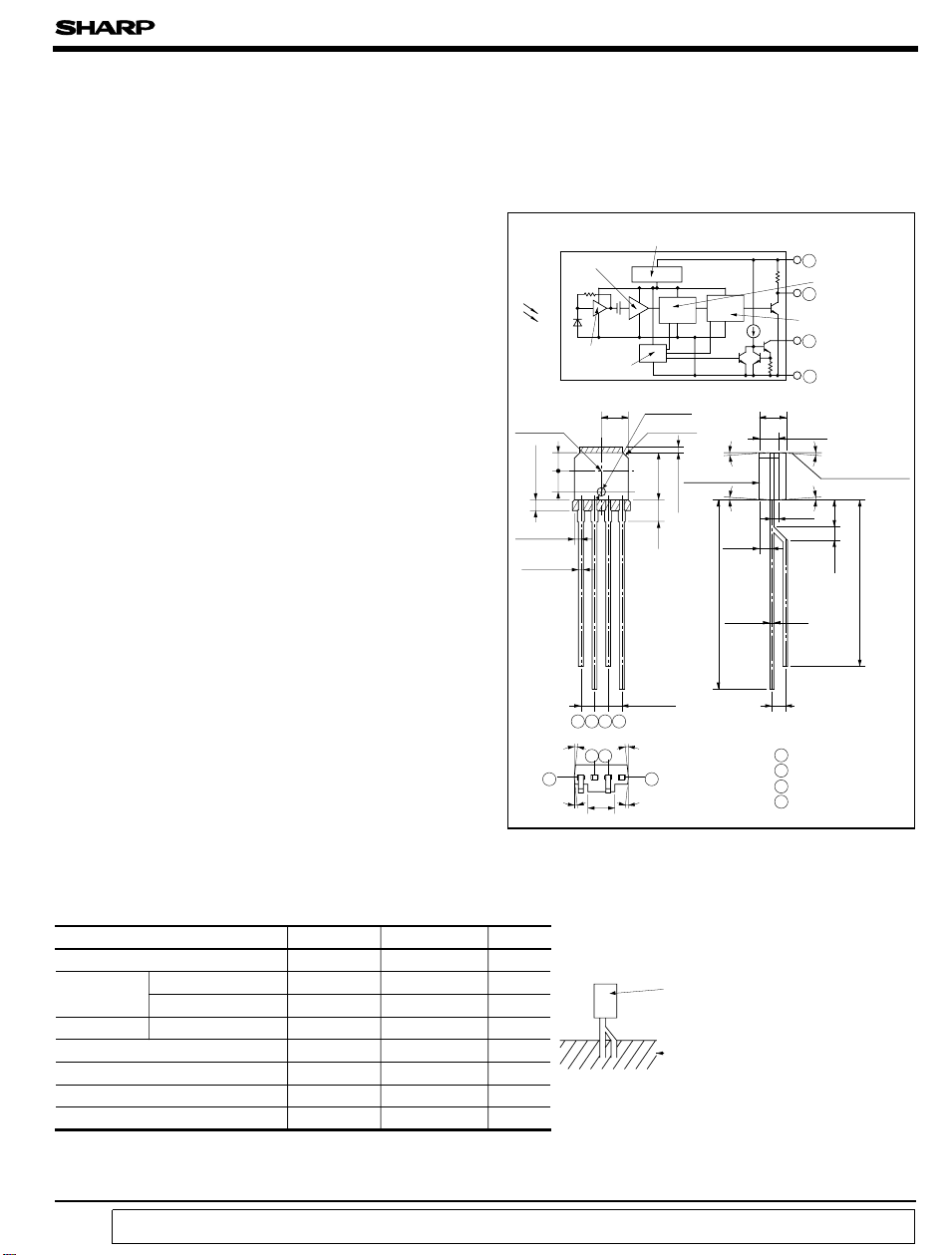
Internal connection diagram
Voltage regulator
Comparator
Amp.
Oscillator
±
0.2
Detector
center
0.3
±
1.7
MAX.
1.8
1.0
MAX.
0.6
4-0.45
1234
6˚
23
1
6˚
2.5
*“OPIC ” (Optical IC) is a trademark of the SHARP Corporation.
An OPIC consists of a light-detecting element and signal processing circuit integrated onto a single chip.
Ta= 25˚C
)
2.5
P= 1.27mm
PPP
φ 0.8
2- C0.5
0.2
±
6˚
4
6˚
4˚
Lustered face
MAX.
4.4
2.0
4˚
0.3
0.95
1.0
±
+0.2
0.4
17.6
-0.1
Resin portion
Soldering portion
(
Immersed up to bending portion
2.5
P
1 V
2 V
3 GND
4 GL
(
Sync.
1
detector
circuit
2
Demodulator
circuit
4
3
±
0.2
±
0.2
1.8
0.45
CC
O
out
Unit: mm
Visible light
4˚
cut-off black
epoxy resin
4˚
2.51.27
1.0
±
15.5
)
)
“ In the absence of confirmation by device specification sheets, SHARP takes no responsibility for any defects that occur in equipment using any of SHARP's devices, shown in catalogs,
data books, etc. Contact SHARP in order to obtain the latest version of the device specification sheets before using any SHARP's device.”

IS471F
■ Electro-optical Characteristics
Parameter Symbol Conditions
Operating supply voltage V
Supply current I
Low level output voltage
Output
High level output voltage
Output short circuit current
GL
output
*5
“Low→High ” threshold irradiance
*5
“High→Low ” threshold irradiance
Hysteresis E
Response
time
*7
External disturbing light illuminance
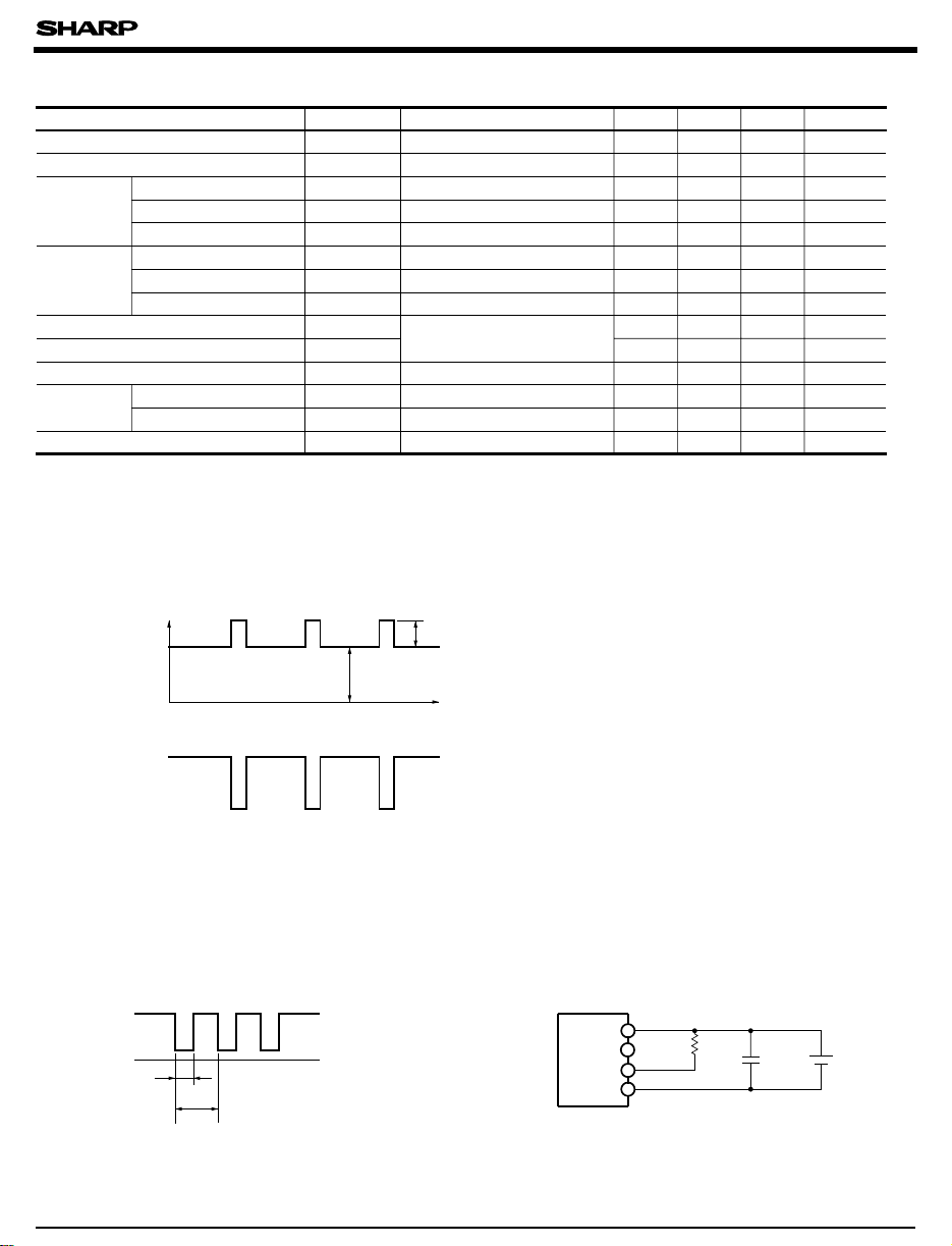
*3 EeP represents illuminance of signal light in sync with the low level timing of output at GL
E
represents illuminance of DC light. For detail, see Fig. 1.
eD
Light source: Infrared light emitting diode (λ p= 940nm
represents illuminance of signal light in sync with the low level timing of output at GL
E
VP
represents illuminance of DC light. Note that the light source is CIE standard light source A.
E
VD
Low level output current
*4
Pulse cycle
*4
Pulse width
“High
→Low”
propagation delay time
“Low→High”
propagation dealy time
Fig.1
E
e
0
Output waveform
at GL
terminal
out
CC
CC
V
OL
V
OH
I
OS
I
GL
t
p
t
W
E
ePLH
E
ePHL
ePLH/EePHL
t
PHL
t
PLH
E
VDX
E
eD
Time
-
VO, GL
terminals shall be opened.
out
IOL= 16mA, E
EVD=EVP=0
EVP=EVD=0
= 500lx, E
VP VD
*3
*3
VGL= 1.2V
-
-
*3
EeD=0
Light emitting
diode (λ p= 940nm
*6
*6
Eep= 7.5 µ W/mm2, *3λ p= 940nm
)
E
eP
(
Note) Fig. 1 shows the output waveform at GL
=0
*6
)
terminal with IS471F connected as shown in
Fig. 3.
(
VCC= 5V, Ta= 25˚C
MIN. TYP. MAX. Unit
4.5 - 16 V
-
*3
3.5 7.0 mA
- 0.15 0.35 V
4.97 - - V
0.25 0.5 1.0 mA
40 55 70 mA
70 130 220 µ s
4.4 8 13.7 µs
- 0.4 2.66
- 0.7 2.8
0.45 0.65 0.95 -
- 400 670 µ s
- 400 670 µ s
2000 7500 -
terminal.
out
terminal.
out
)
2
µ W/mm
2
µ W/mm
lx
out
)
(
t
*4 Pulse cycle
The waveform shown in Fig. 2 is the output voltage waveform at GL
, pulse width
P
(
)
t
are defined as shown in Fig. 2.
W
terminal with IS471F connected as
out
shown in Fig. 3
Fig.2 Fig.3
5V
0V
*5 Defined as Eep that causes the output to go“ Low to High”(or“ High to Low”).
t
W
t
P
IS471F
V
CC
1
V
O
2
GL
4
GND
3
280Ω
out
0.33 µF
5V
 Loading...