


In the absence of confirmation by device specification sheets, SHARP takes no responsibility for any defects that may occur in equipment using any SHARP devices shown in
catalogs, data books, etc. Contact SHARP in order to obtain the latest device specification sheets before using any SHARP device.
1
DESCRIPTION
The IR3Y48M is a CMOS single-chip signal
processing IC for CCD area sensors which includes
correlated double sampling circuit (CDS), clamp
circuit, automatic gain control amplifier (AGC),
reference voltage generator, black level detection
circuit, 20 MHz 10-bit analog-to-digital converter
(ADC), timing circuit for internally required pulses,
and serial interface for internal circuits.
FEATURES
• Low power consumption :
110 mW (TYP.) at 20 MHz mode
• Wide AGC range : 0 to 36 dB
(Gain step : 0.094 dB/step)
• High speed sample-and-hold circuits :
pulse width 10 ns (MIN.)
• Power save operation :
84 mW (TYP.) at 15 MHz mode
• Standby mode : less than 0.3 mW
• Built-in serial interface
• 10-bit ADC operating up to 20 MHz
– Non-linearity
DNL : 0.6 LSB (TYP.)
INL : 1.5 LSB (TYP.)
• Maximum input level of CCD signals : 1.1 Vp-p
• Accepts a direct signal input to ADC or AGC
(input level : 1 Vp-p (TYP.))
• Single +3 V power supply
• Package :
48-pin QFP (QFP048-P-0707) 0.5 mm pin-pitch
PIN CONNECTIONS
IR3Y48M
CCD Signal Process & Digital Interface IC
IR3Y48M
1
48 47 4645 44 434241 40 39 37
13 14 1516 17 1819 20 2122 23 24
2
3
4
5
6
7
8
9
10
11
12
36
35
34
33
32
31
30
29
28
27
26
25
NC
AV
DD4
NC
V
RN
VRP
AVDD2
AVDD2
AVSS2
AVSS2
VCOM
CCDIN
REFIN
OP
RESETN
AVDD3
AVSS3
STBYN
CSN
SDATA
SCK
OBP
CCDCLP
BLK
ADCLP
CLPCAP
ADIN
OBCAP
MONOUT
NC
AISET
AV
DD1
AVSS1
NC
ADCK
SHR
SHD
DO
9
DO8
DO7
DO6
DO5
DVDD
DVSS
DO4
DO3
DO2
DO1
DO0
38
48-PIN QFP
TOP VIEW
(QFP048-P-0707)

IR3Y48M
2
BLOCK DIAGRAM
13
12
CCD
ADIN
ADCLP
CCDCLP
6 dB/STEP
(0 to 12 dB)
S/H
OBCAP
AISET
ADCK
11
14
15
18
22
26 28 27 25 31 29 30 36 35
32
BLK OBP CCDCLP
TIMING
GENERATOR
SERIAL
REGISTER
REGISTER (7-BIT)
COMPARE
10-BIT
ADC
OBP
0.094 dB/STEP
(0 to 6 dB)
6 dB/STEP
(0 to 18 dB)
AGC
ROUGH
AGC
FINE
DAC
ADCLP CSN SCK SDATA OP RESETN STBYN
42
43
33
20
2
34
19
4
10
5
6,7
8,9
DVSS
DVDD
AVSS3
AVSS2
AVSS1
AVDD4
AVDD3
AVDD2
AVDD1
VRN
VCOM
BANDGAP
V
REF
VRP
DO0 to DO9
37 to 41, 44 to 48
MONOUT
16
SHD
24
SHR
CLPCAP
DC
REFIN
CCDIN
CLAMP
CLPCAP
23
CDS
+
IR3Y48M
3
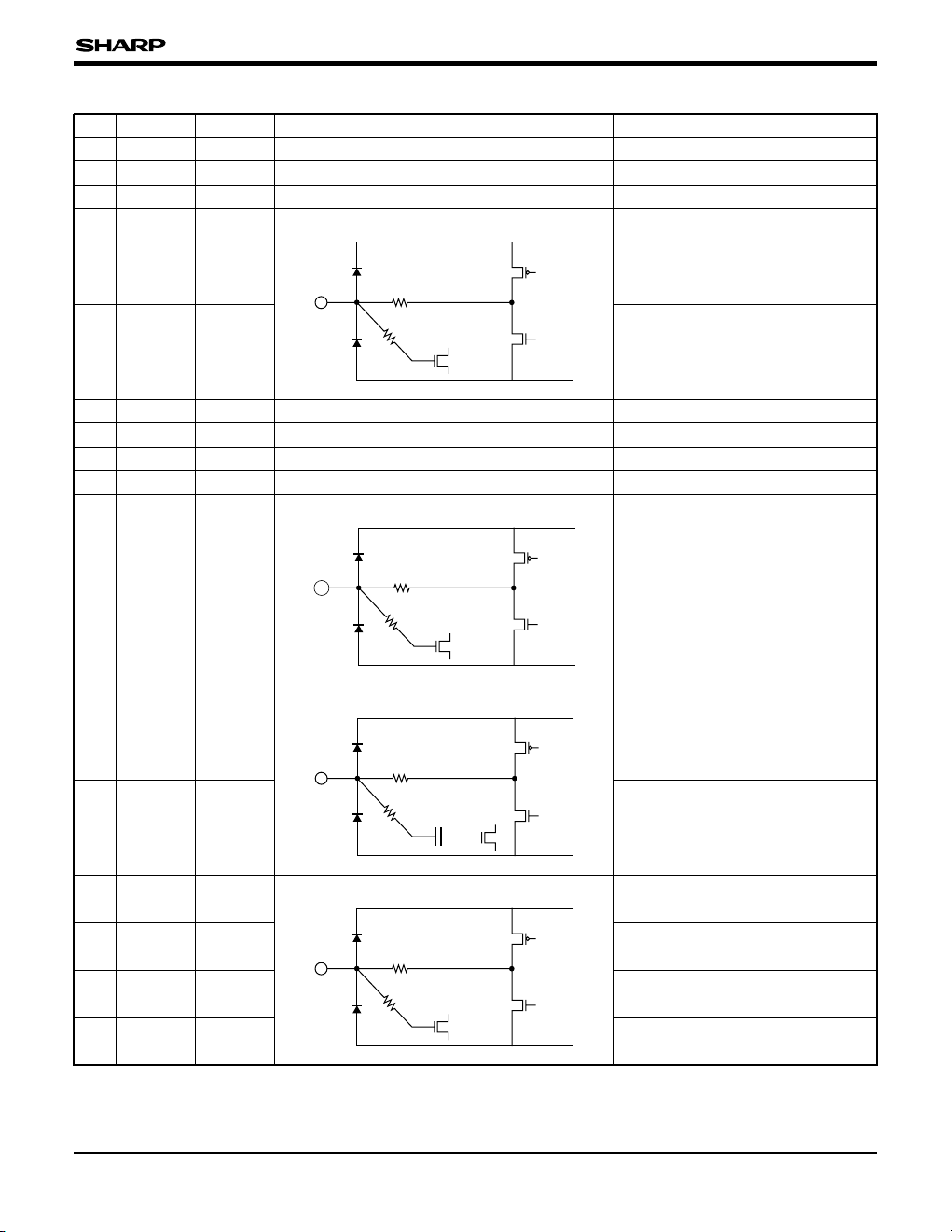
PIN DESCRIPTION
1NC
–
No connection.
PIN NO.
SYMBOL I/O
EQUIVALENT CIRCUIT DESCRIPTION
Supply of 2.7 to 3.6 V analog power.
–AV
DD4
2
3
NC –
No connection.
VDD
GND
◊
ADC internal negative reference
voltage.
(Connect to AV
SS via 0.1 µF.)
OV
RN
4
Supply of 2.7 to 3.6 V analog power.
–AV
DD2
6
5
V
RP O
9
AV
SS2 –
An analog grounding pin.
8
AVSS2 –
An analog grounding pin.
7
AV
DD2 –
Supply of 2.7 to 3.6 V analog power.
ADC internal common reference
voltage.
(Connect to AV
SS via 0.1 µF.)
OV
COM
10
11
CCDIN I
CDS circuit data input.
IREFIN
12
ADC internal positive reference
voltage.
(Connect to AV
SS via 0.1 µF.)
CDS circuit reference input.
VDD
GND
◊
10
VDD
GND
◊
Clamp level output.
(Connect to AV
SS via 0.1 µF.)
OCLPCAP
13
14
15
16
◊ Internal gate
ADIN
OBCAP
MONOUT
I
O
O
ADIN signal input.
Black level integration voltage.
(Connect to AV
SS via 0.033 µF.)
Monitor output of CDS or AGC.
VDD
GND
◊
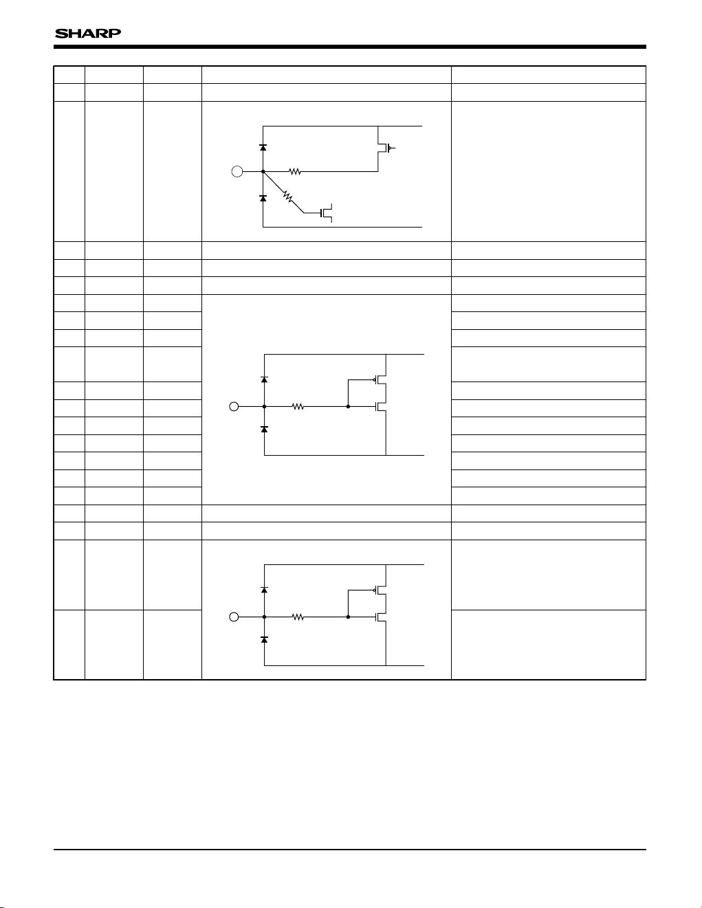
4
IR3Y48M
PIN NO.
SYMBOL I/O
EQUIVALENT CIRCUIT DESCRIPTION
–NC
17 No connection.
Internal analog circuit bias input.
(Connect to AV
SS via 4.7 k$.)
18
AISET I
No connection.21
NC –
An analog grounding pin.
33
AV
SS3 –
An analog grounding pin.20
AV
SS1 –
Supply of 2.7 to 3.6 V analog power.19
AVDD1 –
IADCK
22 ADC sampling clock input.
Reference sampling pulse input.
Data sampling pulse input.
Clamp and black calibration control
for ADIN signal.
Blanking pulse input.
Clamp control input.
Black level period pulse input.
Serial port clock input.
Serial port data input.
Serial port chip selection (active at low).
Standby control (standby at low).
23
24
25
26
27
28
29
30
31
32
SHR
SHD
ADCLP
BLK
CCDCLP
OBP
SCK
SDATA
CSN
STBYN
I
I
I
I
I
I
I
I
I
I
–AV
DD3
34 Supply of 2.7 to 3.6 V analog power.
VDD
GND
◊
18
VDD
GND
◊ Internal gate
Serial I/F operation code enable pin
(active at low).
36
OP I
Reset signal input (reset at low).
35
RESETN I
VDD
GND
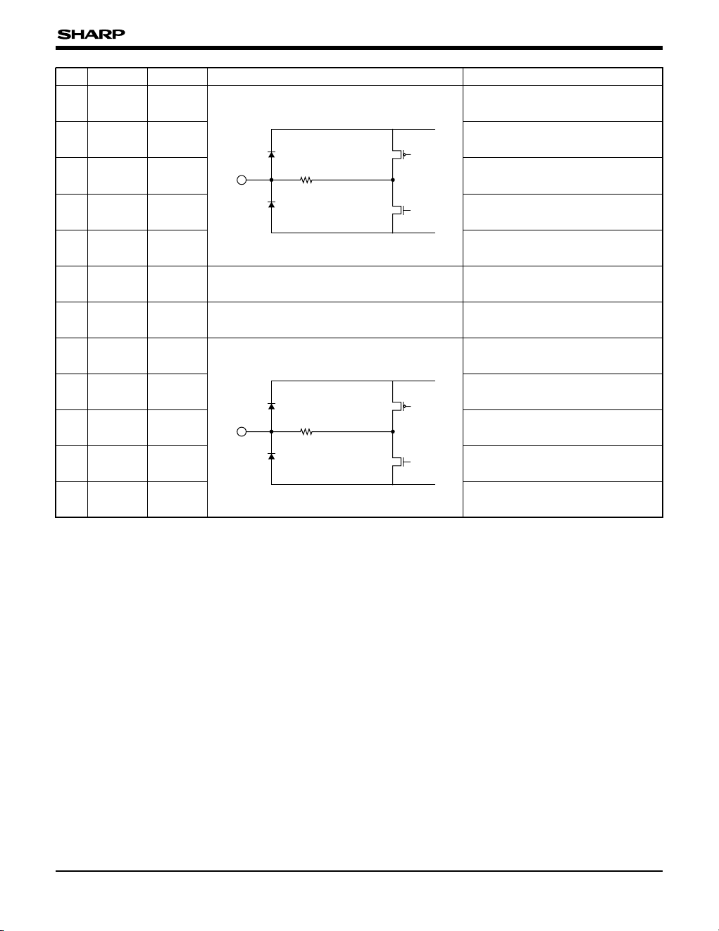
IR3Y48M
5
PIN NO.
SYMBOL I/O
EQUIVALENT CIRCUIT DESCRIPTION
ODO
0
37
ADC digital output (LSB).
(Capable of High-Z)
VDD
GND
41
DO
4 O
ADC digital output.
(Capable of High-Z)
40
DO
3 O
ADC digital output.
(Capable of High-Z)
39
DO
2 O
ADC digital output.
(Capable of High-Z)
38
DO
1 O
ADC digital output.
(Capable of High-Z)
43
DV
DD –
Digital output driver power supply.
(2.7 to 3.6 V)
42
DV
SS –
Digital output driver GND. A digital
grounding pin.
ADC digital output (MSB).
(Capable of High-Z)
ODO
9
48
ADC digital output.
(Capable of High-Z)
ODO
8
47
ADC digital output.
(Capable of High-Z)
ODO
7
46
ADC digital output.
(Capable of High-Z)
ODO
6
45
ADC digital output.
(Capable of High-Z)
ODO
5
44
VDD
GND
NOTES :
• NC pins are recommended to be connected to AVSS on PCB even they are not connected electrically in the chip.
• High-Z at standby.
IR3Y48M
6
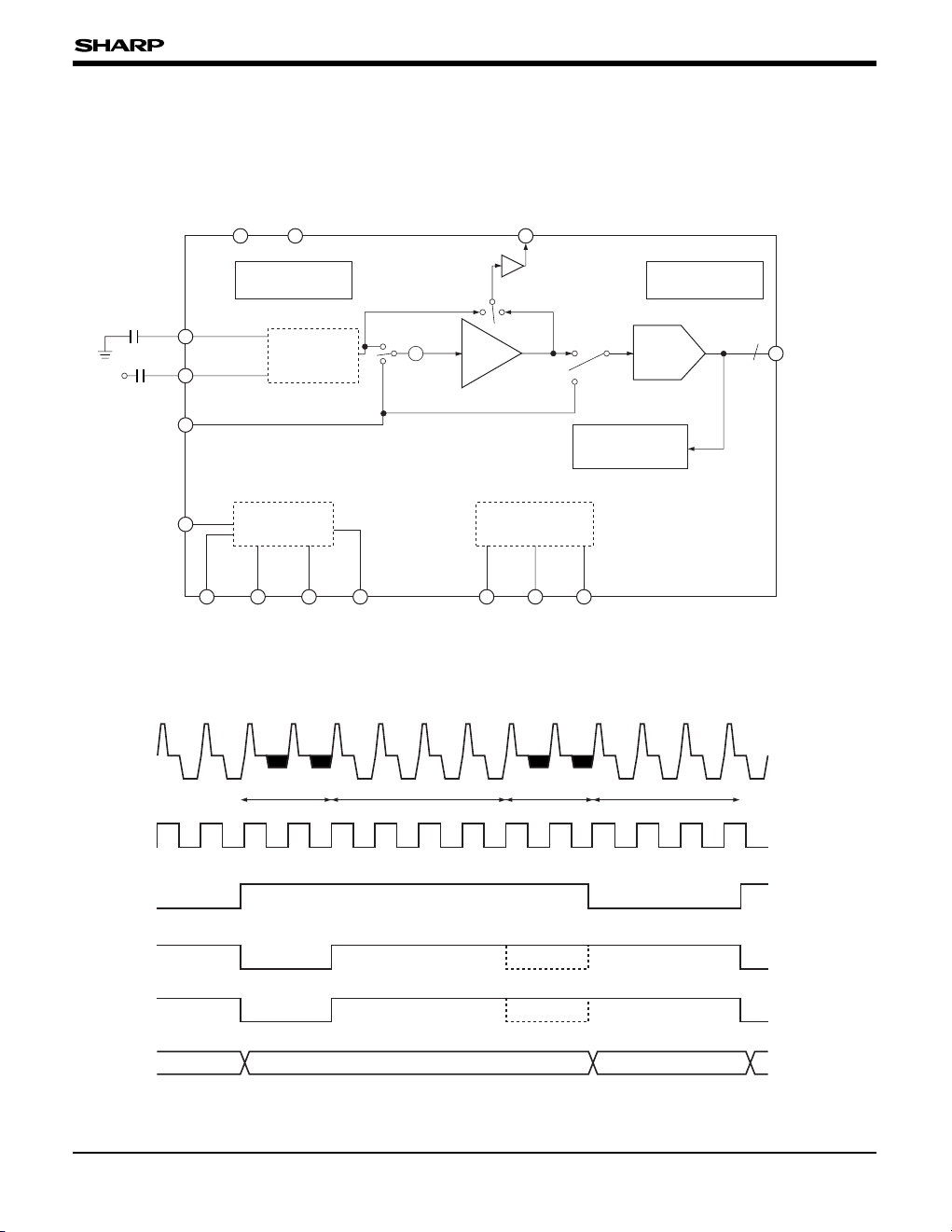
FUNCTIONAL DESCRIPTION
Outline
The configuration of IR3Y48M is described below.
SHR SHD
MONOUT
V
REF
Clamp
CDS
REFIN
CCDIN
ADIN
ADCK
BLK
OBP
CCDCLP ADCLP
CSN
SDATASCK
CCD
AGC
DO
0 toDO9
Black
Control
Serial
Register
Timing
Generator
IR3Y48M
+
10-bit
ADC
CCD
OB Effective Pixel (OB) Blanking
ADCK
BLK
OBP
CCDCLP
Data Output Black Code
DO
0-DO9
GENERAL TIMING
7
IR3Y48M
Reference Clock (SHR)
Data Clock (SHD)
REFIN
CCDINCCD
CDS
CDS Output
= V (CDS)
= V (DAT) – V (PREC)
Reset
Pulse
Reset
Pulse
V (PREC)
V (DAT)
MAX. Level
SHR
SHR
SHD
SHD
SIG
fSMAX = 20 MHz/tSMIN = 50 ns
SIG
V (CDS)
CDS Operation
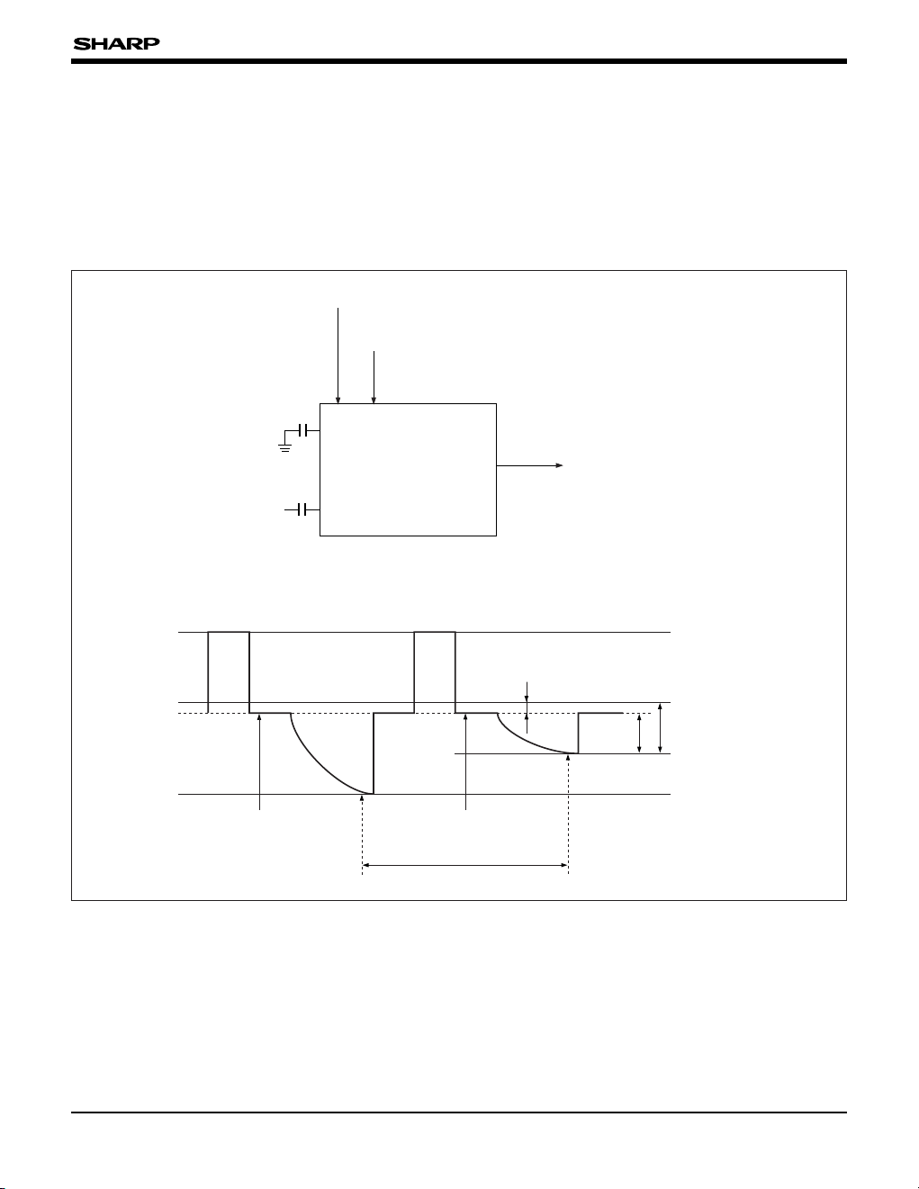
CDS Circuit
CDS circuit holds CCD precharge (reference) level
at SHR pulse, then it samples CCD pixel data at
SHD pulse. Correlated (common) noise is removed
by subtraction of precharge level from pixel data
level.
CDS has the gain of maximum 12 dB (6 dB/step).
This gain is a part of total gain and it is controlled
by register value similar to gain in AGC circuit.
Connect signal from CCD sensor to CCDIN pin
through C-coupling. Place the same capacitor
between REFIN and AV
SS.
8
IR3Y48M
Clamp Circuit
DC CLAMP
DC level of the analog input is fixed by internal DC
clamp circuit. DC level of C-coupled CCD signal at
CDS input is set to CLPCAP by DC clamping.
Normally clamp switch is turned on at black level
calibration period. Place 0.1 µF external
capacitance between CLPCAP and AV
SS.
Timing Control
(Register Conditions)
REFIN
CCDIN
SHR SHD CCDCLP
Clamp
Source
CLPCAP
DC Clamp Function
(CCDCLP)
CLPCAP
CCDCLP
ADCK
CCD
CLPCAP Level
REFIN, CCDIN
Clamp Level
Clamp Timing
CLAMP OF ADIN SIGNAL
Clamp operation for ADIN path is also available.
Note that clamp voltage [CLPCAP] is different
between CCD input and ADIN.
ADCLP signal is used for both clamp and black
level control at ADIN input mode. It is also possible
to turn off clamp operation by register setting.
CLAMP CONTROL
Following items are selectable through register
setting.
a) Clamp current
Normal or fast clamp is selectable for charge
current. (Select normal clamp in general)
b) Clamp target
Input signal (REFIN and CCDIN) to be
clamped is selectable. It is also possible to turn
off the clamp function.
ADCLP
ADIN
To AGC
or
To ADC
Timing Control
CLPCAP
(ADCLP)
ADIN DC Clamp Function
9
IR3Y48M
CDS
REFIN
S/H
CCDIN
ADIN
(Path for ADIN)
ADCLP
ADCLPOBP
OBP
Compare
Register (7-bit)
OBCAP
Rough Fine
DO
0-DO9
AGC AGC
+
DAC
10-bit
ADC
Black Level Calibration
CCD
ADCK
OBP
OBCAP
Previous
Black Level
Blanking Blanking
Effective
Pixel Signal
Effective
Pixel Signal
Optical Black Period
Resulting Black
Calibration Level
(Hold)
Black Level Calibration Timing
Black Level Cancel Circuit
The purpose of black level cancel is to adjust the
AGC input level which can equalize the ADC output
code to black level code written in the register. The
black level cancelling is generally done during OB
(optical black period) pulsed by OBP pulse. The
register value ((1 to) 16 to 127 LSB : default 64
LSB) is written by serial interface.
Black level cancel loop is established while OBP is
low (when pulse is not inverted).
In this loop, ADC output code is compared with
register setting. During OB period, the OBP voltage
gradually terminates into certain voltage resulting
the output code equal to the register setting.
The OBP voltage is discharged under following
status :
q Set black level reset register to 1
w Set RESET pin low
e Power down (by STBYN or register control)
The period to reach the final value depends on the
status of chip. It may take more than one thousand
pixels at start-up or after reset. It may take only
several pixels when the status is not changed. DC
clamp [CCDCLP] is allowed during OBP low.
Black level cancelling for ADIN signal (broken line
in the chart) is controlled by ADCLP pulse (clamp
and OB control are done simultaneously) instead of
OBP.
10
IR3Y48M
Gain Control Circuit
The total gain for CCD input signal covers from 0 to
36 dB.
This range consists of CDS (0 to 12 dB (6 dB/
step)), AGC rough (0 to 18 dB (6 dB/step)), and
AGC fine (0 to 6 dB (0.094 dB/step)). Total gain is
controlled (as described below) by 9-bit gain control
register. The gain is fixed to maximum gain when
the code exceeds 382 (decimal).
The gain of ADIN (which bypassing CDS) is 0 to
24 dB.
0D
0 dB
35.91 dB
0.094 dB
1 step
383D
CDS
6 dB/step
(0 to 12 dB)
Rough
6 dB/step
(0 to 18 dB)
AGC Block
Fine
0.094 dB/step
(0 to 6 dB)
Total Gain = 0 to 35.91 dB
Gain Control

A/D Converter Circuit
IR3Y48M integrates 20 MHz 10-bit full pipeline A/D
converter (ADC).
A/D CONVERSION RANGE
The analog input range of the ADC is determined
by V
REF circuit integrated in IR3Y48M. At ADC
direct input (ADIN) mode (Mode (1) Register D
5 =
1), feed 1 Vp-p (full scale) signal based on clamp
level as zero reference into ADIN input pin.
A/D CONVERTER OUTPUT CODE
(AT MODE (1) REGISTER D
5 = 1)
The digital output format is binary.
Thus, "all zero" digital output with zero reference
input (ADIN = CLPCAP), "all one" digital output with
full-scale input (ADIN = CLPCAP + 1 V (TYP.)).
CLOCK, PIPELINE DELAY AND OUTPUT DIGITAL
DATA TIMING
The A/D conversion is performed based on the
clock fed to ADCK pin.
The track-and-hold operation is completed at falling
(when not inverted) edge of ADCK.
The 10-bit width parallel data is obtained at rising
edge after 5.5 clock pipeline delay. (Sampling edge
is selectable by register setting.)
CODE AT CLAMP LEVEL
(AT MODE (1) REGISTER D
5 = 0, D4 = 1)
The output code at clamp level can be set
throughout (1 to) 16 to 127 LSB at the step of 1
LSB by register setting.
ADC OUTPUT CODE LOGIC
ADC digital output is High-Z under following
conditions :
q Set ADC output register to 1
w Set SYBYN pin low
e Power down (by STBYN or register control)
DIGITAL OUTPUT CODE
According to ADIN, digital codes are determined as
follows :
Data Output at Straight Binary
[Mode (1) Register D
2 = 0, D5 = 1]
11
IR3Y48M
MSB
ADIN DIGITAL CODE
LSB
D9
Clamp
reference
0
:
:0
:1
:
Clamp
reference + 1 V
11
0
1
0
D
0
1
0
1
0
D
1
1
0
1
0
D
2
1
0
1
0
D
3
1
0
1
0
D
4
1
:
0
1
:
0
D
5
1
0
1
0
D
6
1
0
1
0
D
7
1
0
1
0
D
8

12
IR3Y48M
Other Functions
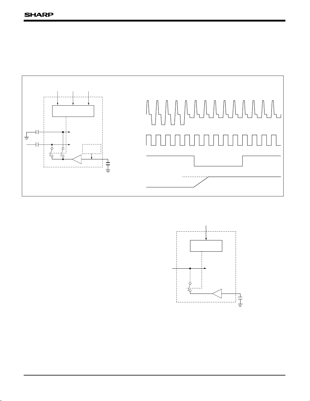
ADC DIRECT INPUT (ADIN MODE)
Direct input path to ADC or AGC is realized by
register setting. This direct path can be turned off
by register. Black level cancel and clamp are
performed at the same timing of ADCLP low.
These controls can be masked by register setting.
BLK, SHR, and SHD controls are ignored at ADIN
mode.
The signal at AGC input is shown below.
Operation at ADC direct input is shown below.
The zero reference (CLPCAP) is established by
ADCLP pulse. The ADIN input range is from
CLPCAP + 1 V (TYP.) (full scale).
ADIN
(N)
N – 8 N – 7 N – 6 N – 5 N – 4 N – 3 N – 2 N – 1 N
(N+1)
(N+2)
ADCK
(When ADCK is inverted,
signal (N) is sampled by this edge)
ADCLP
Black Cancel & Clamp
DO
0-DO9
ADIN Signal Processing (AGC Input)
NOTE : For ADCLP low, both black level cancel and clamp are active at AGC input mode, and only clamp is active at
ADC input mode.
Clamp ON
Full scale CLPCAP + 1 V
ADC
dynamic range
= 1 Vp-p
CLPCAP
ADIN
ADCLP
ADIN Signal Input Level
STANDBY MODE
The standby mode can be set either by register
setting or STBYN pin.
If one of the above is set, IR3Y48M powers down.
("OR" logic)

13
IR3Y48M
MONITOR OUTPUT
By setting the register, the signal from MONOUT is
selectable. Alternatives are OFF, CDS output, AGC
output, or REFIN/CCDIN output. Even at the CDS
gain is set to a certain gain, the CDS output on
MONOUT is multiplied by 1/gain resulting the level
before CDS amplification.
The output level of MONOUT is shown below. The
MONOUT level is V
COM (1.1 V, TYP.) at zero
reference level. For the maximum amplitude (1.1 Vp-p),
the output level is 2.2 V (TYP.).
CAUTION :
VCOM pin does not have enough driving capabilities.
POLARITY INVERSION
Following timing pulse of IR3Y48M control can be
inverted by register setting :
q ADCK (A/D converter sampling pulse)
w SHR, SHD (CDS sampling clock)
e BLK, OBP, CCDCLP, ADCLP (Enable controls)
POWER SAVE
Power save mode is selectable for the sampling
frequency below 15 MHz.
The power consumption at this mode is lower than
20 MHz mode.
General Notice for Power Supply
It is recommended to supply both AVDD and DVDD
supply from single regulator.
(Observe absolute maximum rating specification :
DV
DD ≤ (AVDD + 0.3 V) even at the power-up and
power-down sequence.)
Refer to "APPLICATION CIRCUIT EXAMPLE"
against noise of power supply.
CCD
MONOUT
V
0 = No signal
V
0 = No signal level
MON reference level = VCOM = 1.1 V (TYP.)
V1 V2
MAX. signal = 1.1 V
MAX. level = V
COM + 1.1 V
= 2.2 V
V
3
V1 V2 V3
Monitor Output Level

14
IR3Y48M
Serial Interface Circuit
The internal registers of IR3Y48M are controlled
through 3-wire serial interface.
The 16-bit length control data consists of 2-bit
operation code, 4-bit address, and 10-bit data. The
controller should set each bit synchronizing to SCK
falling since IR3Y48M (receiver) acquire data at
SCK rising edge. The data is valid while CSN is
low.
The written data comes effective at rising edge of
CSN.
Fix CSN to high when no access is conducted.
It is forbidden to write data to the address that is
not listed.
Always give 16 times SCK rising during CSN low.
All data are ignored when SCK rising during CSN
low is less than 16.
The effect of operation code is determined by OP
pin control.
When OP pin is high, the data are always valid
regardless of O
0 and O1.
When OP pin is low, operation code control is
active, and the data is written only when both O
0 =
0 and O
1 = 1 are true.
0 1 2 3 4 5 6 7 8 9 101112131415
CSN
SCK
SDATA
Ope
Code Address Data
O
0 O1 A0 A1 A2 A3 D0 D1 D2 D3 D4 D5 D6 D7 D8 D9
Serial Write Control

15
IR3Y48M
Registers
IR3Y48M has 10-bit x 5 registers to control its
operations.
All registers are write only. The serial registers are
written by serial interface.
Register Map
1. Reference name Mode (1)
2. Register address
[Write]
3. Register bit assignment
A3
R/W
ADDRESS REFERENCE NAME
MAJOR FUNCTIONS [DATA]
A
2 A1 A0
001
Test mode (ADIN coupling mode)
Test register0
W
110
ADC code at black level (1 LSB step)
Black level0
W
010
Total gain
Gain0
W
100
Clamp current/ADIN clamp/Clamp target/S/H, enable logic/Monitor
selection
Mode (2)0
W
000
ADCK polarity/ADIN connection/Frequency mode/ADC output/Black
level reset/Standby
Mode (1)0
W
A
3 A2 A1 A0
0000
D9
Black level reset
ADC output
Frequency mode
ADIN connection
ADCK polarity
X0
D
0
0
D
1
0
D
2
0
D
3
0
D
4
0
D
5
0
D
6
X
D
7
X
D
8
Standby
X : Don't care
<->
<->
<->
<---->
<->
Functions
<->
Default

16
IR3Y48M
4. Register operations
Standby
Black level reset
ADC output
Frequency mode
ADIN connection
0
0
0
0
0
0 0 ADIN function OFF
20 MHz mode
Normal operation [ADC data output]
Normal operation
Normal operation
Normal operation as timing chart
CONTROLS
OPERATIONS NOTE
D
8 D7 D6 D5 D4 D3 D2 D1 D0D9
ADCK polarity
ADCK clock inversion1
ADIN signal to AGC
ADIN signal to ADC
1X0
1
15 MHz mode1
1ADC output High-Z [or logic of STBYN]1
2Black level reset [or logic of RESETN]1
Standby [or logic of STBYN]1
NOTES : X : Don't care
1. ADC output is set to high impedance if one of following case is true.
Case 1 : Set "ADC output" bit to "1".
Case 2 : Set STBYN pin to low.
Case 3 : Set "Standby" bit to "1".
2. Black level integral CAP [OBCAP] is discharged if following case is true.
Case 1 : Set "Black level reset" to "1".
Case 2 : Set RESETN pin to low.

IR3Y48M
17
1. Reference name Mode (2)
2. Register address
[Write]
3. Register bit assignment
4. Register operations
A3 A2 A1 A0
1000
D9
Monitor selection
X : Don't care
S/H, enable logic
Clamp target
ADIN clamp
Clamp current
X0
D
0
0
D1
0
D2
0
D3
0
D4
0
D5
0
D6
0
D7
X
D8
<---->
<---->
<---->
<->
<->
Functions
Default
Monitor selection
S/H, enable logic
Clamp target
ADIN clamp
0
00
10
0
0 Clamp operation active for ADIN
Normal mode [clamp both REFIN & CCDIN]
Clamp CCDIN only
Normal operation as timing chart
Normal clamp
0
CONTROLS
OPERATIONS
D
8 D7 D6 D5 D4 D3 D2 D1 D0D9
Clamp current
Fast clamp1
No clamp for ADIN1
1 Clamp REFIN only0
Clamp OFF11
S/H control polarity inversion 10
1 0 AGC output monitor
0 1 CDS signal to monitor
0 0 Monitor OFF
1 1 Both of S/H and enable inversion
1 0 Enable control polarity inversion
Output REFIN and CCDIN (for calibration)11
NOTE
1
2
3
4
NOTES :
1. The S/H signals are SHR and SHD.
2. The enable controls are BLK, OBP, CCDCLP, and ADCLP.
3. At this mode, monitor output gain = 0 dB regardless of CDS gain.
4. At this mode, monitor output depends on CDS gain.

18
IR3Y48M
1. Reference name Gain
2. Register address
[Write]
3. Register bit assignment
4. Register operations
X : Don't care
A3 A2 A1 A0
0100
D9
Total gain
X0
D
0
0
D1
0
D2
0
D3
0
D4
0
D5
0
D6
0
D7
0
D8
<------------------------------------->
Functions
Default
CONTROLS
DECIMAL NOTE
0Total gain
(For CCDIN input)
D
9 D8 D7 D6 D5 D4 D3 D2 D1 D0
0 0 0 0 0 0 0 0 0 0 0.000
HEX
TOTAL
GAIN (dB)
0.094
0.188
0.281
0.375
5.813
5.906
6.000
6.094
12.000
18.000
24.000
30.000
35.625
35.719
35.813
35.906
35.906
35.906
1
2
3
4
3E
3F
40
41
80
C0
100
140
17C
17D
17E
17F
180
1FF
1
0
1
0
0
1
0
1
0
0
0
0
0
1
0
1
0
1
0
1
1
0
1
1
0
0
0
0
0
0
0
0
1
1
0
1
0
0
0
1
1
1
0
0
0
0
0
0
1
1
1
1
0
1
0
0
0
0
1
1
0
0
0
0
0
0
1
1
1
1
0
1
0
0
0
0
1
1
0
0
0
0
0
0
1
1
1
1
1
0
0
0
0
1
1
0
0
0
0
0
0
1
1
1
1
1
0
0
0
0
π
0
0
1
1
π
0
π
1
π
0
π
1
π
1
1
1
1
0
π
1
0
0
0
0
0
0
0
0
1
1
0
0
0
0
0
0
1
1
0
0
0
0
0
0
0
0
0
0
1
1
1
1
1
1
1
1
1
2
3
4
62
63
64
65
128
192
256
320
380
381
382
383
384
511
1
00

19
IR3Y48M
NOTES :
1. Gain is always (35.90625 dB, TYP.) for code greater than 382 (decimal).
2. Gain is always (23.906 dB, TYP.) for code greater than 254 (decimal).
π
π
π
π2
10010000 650 41 6.094
00100000 1280 80 12.000
00110000 1920 C0 18.000
00010000 640 40 6.000
11001111 630 3F 5.906
01001111 620 3E 5.813
π
00000001 40 4 0.375
11000000 30 3 0.281
01000000 20 2 0.188
10000000 10 1 0.094
00000000 00 0 0.000
CONTROLS
DECIMAL
D
8 D7 D6 D5 D4 D3 D2 D1 D0D9
Total gain
(For AGC input)
NOTEHEX
TOTAL
GAIN (dB)
23.813FE0 25411111110
11111111 5111 1FF 23.906
01000000 2581 102 23.906
10000000 2571 101 23.906
00000000 2561 100 23.906
11111111 2550 FF 23.906

20
IR3Y48M
NOTE :
1. Codes 1 to 15 are available but not recommended black calibration period is specified under 15 < code < 128.
1. Reference name Black level
2. Register address
[Write]
A3 A2 A1 A0
1100
3. Register bit assignment
4. Register operations
D9
Black level
X0
D
0
0
D1
0
D2
0
D3
0
D4
0
D5
1
D6
X
D7
X
D8
Functions
Default
<----------------------------->
X : Don't care
0001000 32 20
0010000 64 40
0011111 124 7C
1100100 19 13
0100100 18 12
100 0 17 11
0000100 16 10
1100011 15 F 1
π1
1000000 1 1 1
000 0 0 0 0 FORBIDDEN FORBIDDEN
OPERATIONS [ADC CODE : BINARY]
DECIMAL
B
8 B7 B6 B5 B4 B3 B2 B1 B0B9
Black level
NOTEHEX
7E1261111110
1111111 127 7F
π
π
π
1011111 125 7D
100

IR3Y48M
21
1. Reference name Test register
2. Register address
[Write]
A3 A2 A1 A0
0010
3. Register bit assignment
D9
ADIN test mode
X0
D
0
0
D1
0
D2
0
D3
0
D4
0
D5
0
D6
X
D7
X
D8
Functions
Default
<->
4. Register operations
Test register (D
6) is prepared for ADIN AC coupled
input. Using this mode the signal center is set to
V
COM. No clamp signals are required at this mode.
Connect C-coupled output to ADIN. The resistance
50 k$ between ADIN (14 pin) and CLPCAP (13
pin) stabilize the DC level at ADIN pin.
0 Normal operation
CONTROLS
OPERATIONS
D
8 D7 D6 D5 D4 D3 D2 D1 D0D9
ADIN test mode
VCOM centered ADIN for AC coupling1
X : Don't care
NOTE :
D5 to D0 must always be "0".

22
IR3Y48M
ABSOLUTE MAXIMUM RATINGS (AVSS = DVSS = 0 V, all voltages are with respect to GND.)
RECOMMENDED OPERATING CONDITIONS
(AVSS = DVSS = 0 V, all voltages are with respect to GND.)
PARAMETER SYMBOL CONDITIONS UNIT
Power supply voltage
AV
DD V–0.3 to +4.5
RATING
DV
DD –0.3 to +4.5 or AVDD + 0.3 V
mA±10Except PSI
IN
0.3 VDVDD – AVDDVDLTVoltage difference
Analog input voltage V
INA VAVSS – 0.3 to AVDD + 0.3
AV
SS – 0.3 to AVDD + 0.3 VVINL
Digital input voltage
(Input pin)
V
Digital input voltage
(Output pin)
AV
SS – 0.3 to AVDD + 0.3
˚C
VONL
Operating temperature
˚C
TOPR
Storage temperature TSTG –40 to +125
–30 to +85
2
1
NOTE
PARAMETER SYMBOL CONDITIONS TYP.
Supply voltage
At start-up, turn on AVDDbefore (or at
the same time as) turning on DV
DD
.
3.02.7
MIN.
V
UNIT
3.6
MAX.
AVDDAnalog
Digital output DV
DD AVDD V2.7 3.0
NOTES :
1. The higher voltage of 4.5 V and AVDD + 0.3 V specifies
maximum value of DV
DD absolute maximum rating.
2. The V
ONL limits the excess voltage applied to digital
output pins.
WARNING :
Operation at or beyond these limits may result in permanent
damage to the device. Normal operating specifications are
not guaranteed at these extremes.
Input current
ELECTRICAL CHARACTERISTICS
Supply Current
(TA = +25 ˚C, AVDD = DVDD = 3.0 V)
NOTES :
1. Specified under monitor function off.
2. Measured under no analog input and clock fixed at low.
PARAMETER SYMBOL CONDITIONS TYP.
Supply current at
normal operation
28
MIN.
mA
UNIT
34
MAX.
I
A15Analog
Digital I
D15 6mA3
I
D20Digital
IA20Analog
fs = 15 MHz
(At 15 MHz mode)
fs = 20 MHz
(At 20 MHz mode) 3.5 mA7
36 mA44
NOTE
1
Supply current at monitor active I
PE (At 20 MHz mode) 46 mA38
mA0.1 2IPDSupply current at power down

NOTES :
1. Normally : Signal path through CDS/AGC/ADC
In this case analog input range is downward
from clamp voltage.
ADIN : Signal bypassing CDS (Direct AGC or ADC
input)
In this case analog input range is upward
from clamp voltage.
2. Specified at MONOUT pin. The noise bandwidth is 100
kHz to 5 MHz.
3. Bandwidth from CCDIN/REFIN to ADC. The bandwidth
is specified as the settling time of ADC output for step
input (full scale – 1 dB) response (at gain = min.).
4. Black calibration period is the period of stabilization of
output code within ±1 LSB (average) compared to register
value for the black level code of 0 to 50% of the full scale
input. (Assuming external capacitance = 0.033 µF.)
External capacitor value to OBCAP pin determines the
bandwidth of the black level cancel loop. Since the gain
of the loop depends on sampling frequency, the
maximum frequency (settling within certain pixels) and
the minimum frequency (avoiding oscillation of the circuit)
are defined.
5. Select the external capacitor referring the following list
based on the minimum and maximum operating
frequencies.
If the black level settling specification (within 2 000
pixels) could be ignored, the maximum sampling
frequency for 0.1 µF and 0.33 µF will extend according
to the increment.
IR3Y48M
23
Analog Specifications
(Unless otherwise specified, AVDD = DVDD = 3.0 V, TA = +25 ˚C, signal frequency fIN = 1 MHz,
signal level = –1 dB (full scale))
The current direction flowing into the pin is positive direction.
CDS & CLAMP CIRCUITS (Sampling frequency f
S = 20 MHz)
PARAMETER SYMBOL CONDITIONS TYP.MIN. UNITMAX. NOTE
Analog input range
V
ICDS Normally Vp-p1.1
100 µV
rms
1
At fs = 20 MHz
NIInput referred noise
V
IAI At ADIN
At gain = max.
At gain = min.
1.1
400
Vp-p
µV
rms
Input capacitance CIN CCDIN, ADIN & REFIN pF15
CBW 1 pixel 3
2
Input Bandwidth
Clamp voltage
V1.951.81.65Normally
V
CLPCAP
At ADIN 1.3 V
Black calibration period 4, 5pixel2000t
BKCAL
1.15 1.45
PARAMETER MODE OBCAP MAX.MIN.
Available
sampling
frequency
20 MHz
mode
7.6 200.033 µF MHz
UNIT
MHz0.33 µF 1.70.6
MHz0.1 µF 5.72.2
MHz0.033 µF 155.8
15 MHz
mode

24
IR3Y48M
NOTES :
1. Gain is specified for gain between AGC input and MONOUT output.
2. Gain measured at MONOUT pin.
PARAMETER
TOTAL GAIN
SYMBOL CONDITIONS TYP.MIN. UNITMAX. NOTE
At normal operation
G
MNN Gain between
REFIN/CCDIN and
MONOUT
0.1 dB–1.9 –0.9
1G
MXN 34.906 35.906 36.906 dB
Min. gain
Max. gain
Gain step dB0.1880.0940GST
At ADIN operation
G
MNNA
Gain between ADIN and
MONOUT
0.7 dB–1.3 –0.3
1G
MXNA 22.906 23.906 24.906 dB
Min. gain
Max. gain
Gain step dB0.1880.0940GSTA
CDS and AGC total gain relative
accuracy
ER
PA ±1 LSB 2
PARAMETER SYMBOL CONDITIONS TYP.MIN. UNITMAX. NOTE
Resolution RES 10 bits
S/N SN dB58
±1.5 LSB±2.5
fs = 20 MHz
(At 20 MHz mode)
fs = 15 MHz
(At 15 MHz mode)
INLIntegral non-linearity
Differential non-linearity DNL ±1.0 LSB±0.5
116 LSB127CCAL
ADC output black level
calibration code
1 LSBST
CALBlack level step
0.850.75 V0.95V
RNVREF voltage (negative)
1.351.25 V1.45V
RPVREF voltage (positive)
1.11.0 V1.2VCOMADC common voltage
56 dBSNDS/ (N+D)
A/D CONVERTER CIRCUIT (fS = 20 MHz. Signal is given to ADIN.)
NOTE :
1. Black level calibration period (tBKCAL) is specified for code = 16 to 127 LSB.
Although black level code of 1 to 15 could be set, t
BKCAL is not guaranteed for these codes.

25
IR3Y48M
Switching Characteristics
(AVDD, DVDD = 2.7 to 3.6 V, AVSS, DVSS = 0 V, TOPR = –30 to +85 ˚C, CL < 10 pF)
PARAMETER SYMBOL CONDITIONS TYP.MIN. UNITMAX.
Conversion speed f
S 20 MHz0.5
ns35t
DL2
ADC output data delay
NOTES :
1. When SHR› is earlier than ADCKfi, assumed positive.
(In the above table, SHR› can be delayed a maximum of 3 ns behind ADCKfi.)
2. When SHD› is earlier than ADCK›, assumed positive.
(In the above table, SHD› can be delayed a maximum of 3 ns behind ADCK›.)
2nstDL1
Tristate enable delay 20 ns
High-Z/Active
tDLE
Tristate disable delay 20 ns
Active/High-Z
tDLD
Enable pulse hold 10 nstHE
Enable pulse setup 10 nstSUE
Data pulse hold 5 nstHD
Data sampling delay ns4tDD
Reference sampling delay ns4tDR
Min. data pulse 10 nstWD
Min. reference pulse 10 nstWR
Clock high period 23 nstH
Clock low period 23 nstL
Clock fall time ns2
(70%/30%) AV
DD, DVDD
tF
ns2
(30%/70%) AV
DD, DVDD
tR
Clock cycle period 50 nstCYC
Clock rise time
Reference pulse setup t
SUR ns–3 1
NOTE
Reference pulse hold
Data pulse setup –3
5
ns
ns
t
SUD
tHR
2

IR3Y48M
26
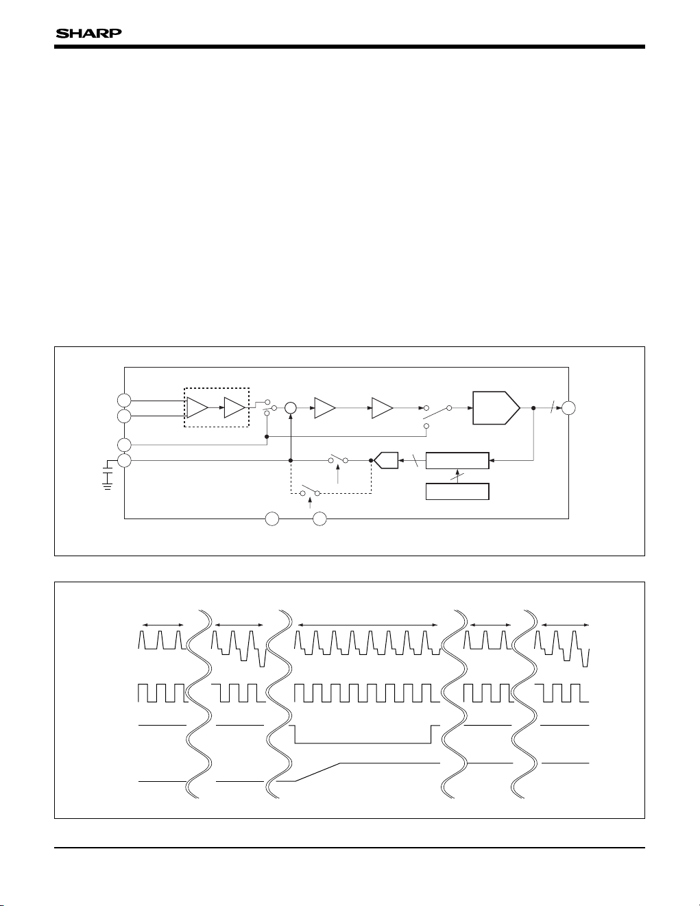
TIMING CHART
ADCK
ADC Input
Sampling Point
N
N + 1
N – 6 N – 5 N – 2 N – 1
N
N + 4
N + 5
N + 6
5.5 clk
delay
Digital Output
t
DL1
0.7DVDD
0.7AVDD
0.3DVDD
0.3AV
DD
tDL2
ADIN : ADC Direct Input
CCD
Reference sampling
Data sampling
SHR
SHD
DO
0-DO9
tHE tSUE
BLK
OBP
CCDCLP
ADCLP
ADCK
tDL
tH
tCYC
tL
tDR tDD
tWR
tWD
tSUDtHD
tSURtHR

IR3Y48M
27
tF
tL
tH
0.7AVDD
0.3AVDD
tCYC
tR
Clock Waveform
ADCK
[When ADCK Inverted by Register]
ADC Input
Sampling Point
N
N + 1
N – 6 N – 5
N – 2 N – 1 N
N + 4
N + 5
N + 6
Digital Output
t
DL1
0.7DVDD
0.7AVDD
0.3DVDD
0.3AVDD
tDL2
6.0 clk
delay
NOTE : At default condition of ADIN mode, falling edge of sampling and rising edge of data out are selected. If each edge
should be a rising edge, invert the ADCK by register setting. (The figure shown on the previous page is the default, the
following is the inverted one.)

IR3Y48M
28
0.7DV
DD
VIOH = –1 mAVOHOutput "High" voltage
Input "High" voltage V
0.7AV
DD
VIH1
PARAMETER SYMBOL CONDITIONS TYP.MIN. UNITMAX.
SCK clock cycle time f
SCYC 10 MHz
Serial data number 16 pcsSNUM
SCK, CSN fall time ns6
70%/30%
t
SF
SCK, CSN rise time ns6
30%/70%
tSR
Hold time 20 nstSH
Setup time 20 nstSSU
40 nstSHI
40 nstSLO
SCK clock high width
SCK clock low width
PARAMETER SYMBOL CONDITIONS TYP.MIN. UNITMAX.
µA±10
µA±10
Output "Low" voltage V
0.3DV
DD
V
0.3AV
DD
High-Z leakage current IOZ
"High" leakage current ILING
IOL = 1 mAVOL
VIL1Input "Low" voltage
1
NOTE
CONTROL INTERFACE TIMING
(AV
DD, DVDD = 2.7 to 3.6 V, AVSS, DVSS = 0 V, TOPR = –30 to +85 ˚C)
tSSU
O0 O1 A0 π
SNUM
D
8 D9
fSCYC
tSLO tSHI
tSH
tSSU tSH
CSN
SCK
SDATA
50%DV
DD
50%DVDD
50%DVDD
Serial I/F Timing
Digital DC Characteristics
(AVDD, DVDD = 2.7 to 3.6 V, AVSS, DVSS = 0 V, TOPR = –30 to +85 ˚C, measured as DC characteristics.)
NOTE :
1. Specified for SHD, SHR, ADCK, BLK, OBP, CCDCLP, ADCLP, CSN, SCK, SDATA, RESETN, STBYN, and OP.

IR3Y48M
29
Data Output Sequence
Pixel Data Readout Sequence (1) : Conversion Start
Pixel Data Readout Sequence (2) : Conversion End
CCD
012345678
SHR
SHD
BLK
Black Level Code
01 2
3
ADCK
DO
0-DO9
CCD
DO
SHR
SHD
ADCK
BLK
0-DO9
(N – 1) (N)
N – 8 N – 7 N – 6 N – 5 N – 4 N – 3 N – 2 N – 1 N

IR3Y48M
30
APPLICATION CIRCUIT EXAMPLE
The following schematic is the reference circuit for
system design.
Optimize capacitance and resistance according to
the system environment.
36 35 34 33 32 31 30 29 28 27 25
123456789101112
37
38
39
40
41
42
43
44
45
46
47
48
24
23
22
21
20
19
18
17
16
15
14
13
DO
0
DO1
DO2
DO3
DO4
DVSS
DVDD
DO5
DO6
DO7
DO8
DO9
SHD
SHR
ADCK
NC
AVSS1
AVDD1
AISET
NC
MONOUT
OBCAP
CLPCAP
ADIN
OP
RESETN
AVDD3
AVSS3
STBYN
CSN
SDATA
SCK
OBP
CCDCLP
BLK
ADCLP
26
REFIN
CCDIN
V
COM
AVSS2
AVSS2
AVDD2
AVDD2
VRP
VRN
NC
AV
DD4
NC
ANALOG
DIGITAL
CHIP
CONTROL
0.1 µF
SIO
CONTROL PULSE
0.1 µF
0.1 µF
0.1 µF
0.1 µF
0.1 µF
0.1 µF
0.1 µF
0.1 µF
0.1 µF
0.033 µF
4.7 k$
0.1 µF
TOP VIEW
MONITOR
ADIN
SAMPLING
PULSE
CCD
3 V (TYP.)
10 µF
DIGITAL
OUT
0.1 µF
+

PACKAGES FOR CCD AND CMOS DEVICES
31
36
25
37
48
121
0.15
±0.05
0.1
±0.1
9.0
±0.3
7.0
±0.2
7.0
±0.2
(1.0)(1.0)
(1.0)
(1.0)
0.5
TYP.
0.2
±0.08
9.0
±0.3
0.65
±0.2
1.45
±0.2
24
13
Package
base plane
8.0
±0.2
0.08
0.1
M
48 QFP (QFP048-P-0707)
PACKAGE (Unit : mm)
 Loading...