In the absence of confirmation by device specification sheets, SHARP takes no responsibility for any defects that may occur in equipment using any SHARP devices shown in
catalogs, data books, etc. Contact SHARP in order to obtain the latest device specification sheets before using any SHARP device.
1
DESCRIPTION
The IR3Y38M is a bipolar single-chip signal
processing IC for CCD area sensors which includes
correlated double sampling circuit (CDS), clamp
circuit, automatic gain control amplifier (AGC),
reference voltage generator, black level detection
circuit, 10-bit analog-to-digital converter (ADC), and
serial interface for internal circuits.
FEATURES
• Low power consumption : 315 mW (TYP.)
• Wide AGC range : 12 to 43.5 dB
• High speed sample-and-hold circuits :
pulse width 12 ns (MIN.)
• Built-in standby mode for power saving
applications
• Built-in serial interface to control the AGC gain,
maximum gain and offset adjustment
• 10-bit ADC operating up to 18 MHz
• Digital interface for operating 3.3 V logic ICs
• Single +5 V power supply
• Package :
48-pin QFP (QFP048-P-0707) 0.5 mm pin-pitch
PIN CONNECTIONS
IR3Y38M
CCD Signal Process & Digital Interface IC
IR3Y38M
1
48 47 4645 44 4342 41 4039 37
13 14 1516 17 1819 20 2122 23 24
2
3
4
5
6
7
8
9
10
11
12
36
35
34
33
32
31
30
29
28
27
26
25
DO
0
DO1
DO2
DO3
DO4
GND6
VCC6
DO5
DO6
DO7
DO8
DO9
VCC2
Ô
OFSCTL
OBCAP
Î
fl/H
3
fl/H2
fl/H1
Â
‰
REFCAP
V
CC1
ADCK
GND
5
VCC5
SCK
V
CC4
GND4
SDATA
CLPCAP
CCDIN
REFIN
GND
1
SHISET
V
LOGIC
VRB
VRT
ÅNCADIN
ADOFS
AGCCTL
GND3AGCOUT
V
CC3
GND2
38
48-PIN QFP
TOP VIEW
(QFP048-P-0707)

IR3Y38M
2
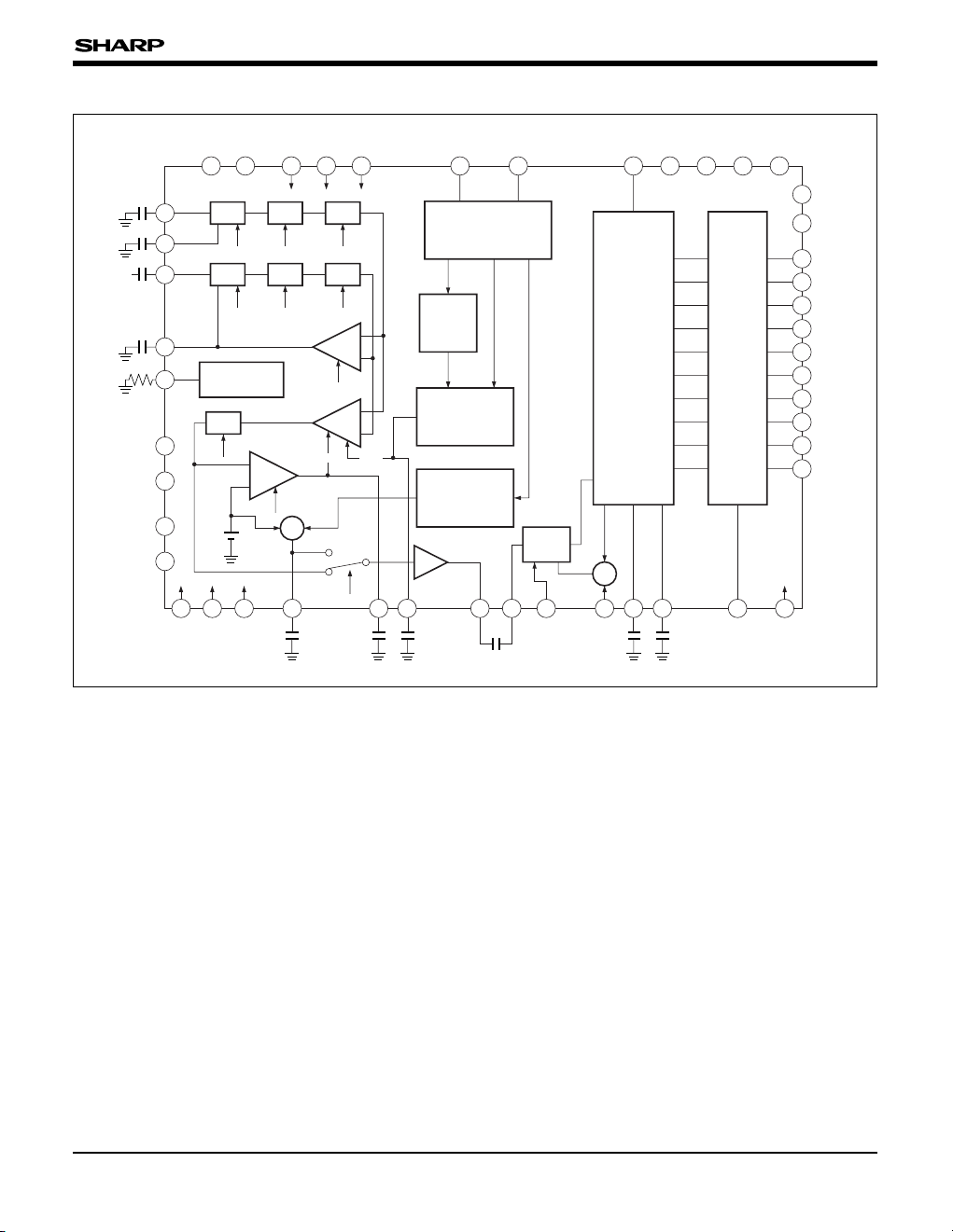
BLOCK DIAGRAM
CLAMP
6-BIT
OFFSET CONTROL
D/A CONVERTER
8-BIT
AGC GAIN CONTROL
D/A CONVERTER
MAX. GAIN
SELECTOR
SERIAL
PARALLEL
CONVERTER
25 23 28 29 30 16 19 13 17 18 15 14
V
CC1 GND1 Â fl/H1 SCK SDATA ADCK VCC4 GND4 VCC5 GND5fl/H2
7
6
12
11
10
9
8
5
4
3
2
1
V
CC6
GND6
DO9
DO8
DO7
DO6
DO5
DO4
DO3
DO2
DO1
DO0
2748464742454339413334353231
‰
V
LOGICVRTVRB
ADOFS
Å
ADIN
AGCOUTAGCCTL
OBCAP
OFSCTL
ÔÎfl/H3
40
38
37
36
24
20
21
26
22
GND
3
VCC3
GND2
VCC2
SHISET
CLPCAP
CCDIN
REFCAP
REFIN
CLAMP
S/H1 S/H2
CLP
fl/H
1
fl/H2
CLAMP
S/H1 S/H2
CLP
fl/H
1
OBP
OBP
BLK
fl/H
2
OUTPUT
BUFFER
BIAS ERROR
AMP
AGC
AMP
CLAMP & S/H
CURRENT SETUP
S/H3
fl/H3
BIAS GAIN
+
–
+
–
+
–
+
+
10-BIT
A/D
CONVERTER

3
IR3Y38M
PIN DESCRIPTION
(The voltage is measured on condition that VCC1 to VCC6 = +5.0 V, VLOGIC = +3.3 V.)
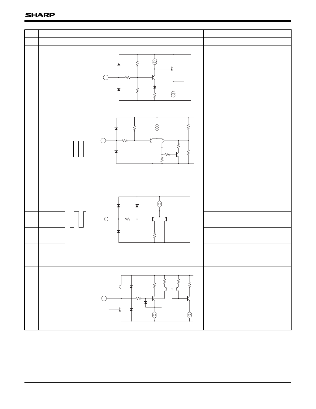
1
DO
0
Digital data output pins of the A/D
converter. DO0 is LSB.
The data format is a straight binary
code.
V
OL : 0.2 V (TYP.)
V
OH : VLOGIC – 0.2 V (TYP.)
PIN NO.
PIN NAME VOLTAGE
EQUIVALENT CIRCUIT DESCRIPTION
200
VCC6
GND6
500
10 k
GND pin of the output buffer of the
A/D converter.
0.0 V
GND
6
6
7
V
CC6
5.0 V
200
VCC6
GND6
500
10 k
Digital data output pins of the A/D
converter. DO9 is MSB.
The data format is a straight binary
code.
V
OL : 0.2 V (TYP.)
VOH : VLOGIC – 0.2 V (TYP.)
DO
5
8
VCC5
200
150 µ
GND5
13
Clock input pin of the A/D
converter.
The A/D conversion is executed at
the rising edge of the ADCK, and
the data is output at the falling edge
of the ADCK.
Duty : 50%
fmax : 18 MHz (MIN.)
ADCK
13
DO
1
DO2
DO3
DO4
2
3
4
5
9
10
11
12
DO
6
DO7
DO8
DO9
14
GND
5
0.0 V
Digital GND pin of the A/D
converter.
Digital power supply pin of the A/D
converter.
5.0 V
V
CC5
15
Power supply pin of the output
buffer of the A/D converter.
16
SCK
Clock input pin of the serial
interface.
Refer to "TRUTH TABLE" of pin 19.
VCC1
200
15 µ
GND1
16
3.1 V
0.2 V
3.1 V
0.2 V
> 2.1 V
< 0.7 V
> 2.1 V
< 0.7 V

IR3Y38M
4
17
V
CC4
5.0 V
Analog power supply pin of the A/D
converter.
PIN NO.
PIN NAME VOLTAGE EQUIVALENT CIRCUIT DESCRIPTION
Analog GND pin of the A/D
converter.
0.0 V
GND
4
18
19
SDATA
Data input pin of the serial
interface.
TRUTH TABLE
VCC1
200
15 µ
GND1
19
VCC1
200
100 µ
GND1
20
Bias decoupling pin of the CDS
signal clamp circuit. This pin is
connected to the GND
1 via a
capacitor.
3.2 V
CLPCAP
20
SDATA
1
0
DATA SHIFT
–
STORE
Action
›
fi
fi
SCK
23
GND
1
0.0 V
GND pin of the CDS/AGC.
Pay careful attention to board
layout of the GND
1 because the
CDS/AGC are noise-sensitive
circuitry.
21
CCDIN
2.5 V
Signal input pin of the CDS.
Input CCD signal to this pin via a
capacitor.
26 k
26 k
VCC1
200
150 µ
150 µ
GND1
2.5 V
REFIN
22
Reference input pin of the CDS.
This pin is connected to the GND
1
via a capacitor.
13 k
200
2 k
2 k
26 k
VCC1
GND1
24
Operation current setting pin of the
CDS and fl/H3 circuits.
This pin is connected to the GND
1
via a resistor.
The slew rates of the fl/Hs are in
inverse proportion to the value of
the resistor.
1.7 V
SHISET
24
> 2.1 V
< 0.7 V

IR3Y38M
5
25
V
CC1 5.0 V
Power supply pin of the CDS/AGC.
PIN NO.
PIN NAME VOLTAGE
EQUIVALENT CIRCUIT DESCRIPTION
200
63 k
36 k
2 k
150 µ
75 µ
VCC1
GND1
26
Bias decoupling pin of the CDS
reference clamp circuit.
This pin is connected to the GND
1
via a capacitor.
3.2 VREFCAP
26
27
‰
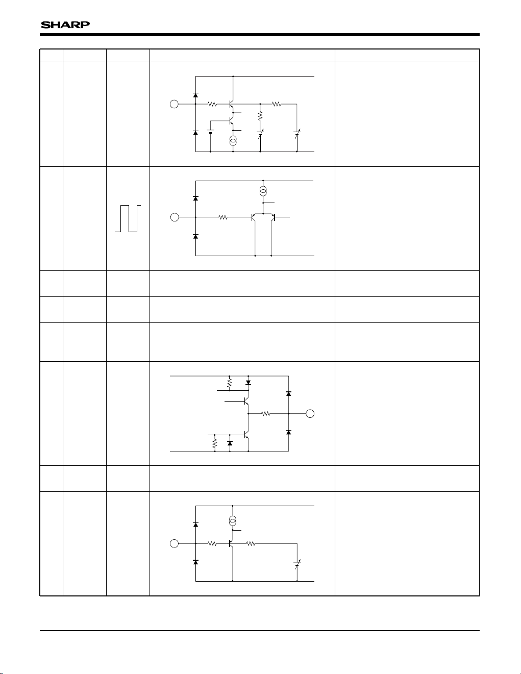
Standby function control pin. All
actions stop and the power
consumption is decreased when
low.
The threshold voltage has 0.4 V
hysteresis.
Connect to the Vcc if not used.
68 k
75 k
65 k
32 k
110 k
VCC1
200
10 k
40 µ
GND1
27
VCC2
200
80 µ
GND2
20 k
3.3 k
20 k
3.3 k
80 µ
33
Clamp capacitor pin of the optical
black clamp (OPB clamp) circuit.
Connect to the GND
2 via a
capacitor.
3.7 VOBCAP
33
100
VCC1
200
50 µ
GND1
Pulse input pin of the CDS feedthrough level clamp.
Signal is clamped when low.
Â
28
29
30
31
32
fl/H
1
fl/H2
flH3
Î
Pulse input pin of the OPB clamp
and bias error amplifier.
Signal is clamped when low.
Pulse input pin of the fl/H
3.
Signal is sampled when low.
Pulse input pin of the fl/H
2.
Signal is sampled when low.
Pulse input pin of the fl/H
1.
Signal is sampled when low.
> 2.1 V
< 0.7 V
5.0 V
(open)
> 2.1 V
< 0.7 V

IR3Y38M
6
34
OFSCTL
2.15
to
2.30 V
Decoupling capacitor pin of the
blanking offset control D/A
converter. Connect to the GND
1 via
a capacitor.
PIN NO.
PIN NAME VOLTAGE
EQUIVALENT CIRCUIT DESCRIPTION
VCC1
200 30 k
100 µ
GND1
D/A2.2 V
10 k
34
VCC2
200
20 µ
GND2
35
VCC3
GND3
20
300
10 k
39
Blanking pulse input pin.
The output of the AGCOUT pin is
blanked when low. The blanking
level can be controlled by the serial
interface.
Ô
35
36
V
CC2 5.0 V
Power supply pin of the fl/H
3 and
OPB clamp circuits.
GND pin of the fl/H
3 and OPB
clamp circuits.
0.0 VGND
2
37
38
V
CC3 5.0 V
Power supply pin of the output
buffer circuit connected to the
AGCOUT pin.
Signal output pin of the AGC.
Connect to the ADIN pin via a
capacitor.
0.9 V
(Î = L)
AGCOUT
39
VCC1
200 11 k
50 µ
GND1
D/A
41
Decoupling capacitor pin of the
AGC gain control D/A converter.
Connect to the GND
1 via a
capacitor.
2.5
to
3.8 V
AGCCTL
41
40
GND
3 0.0 V
GND pin of the output buffer circuit
connected to the AGCOUT pin.
> 2.1 V
< 0.7 V

IR3Y38M
7
42
ADOFS
3.3 V
(open)
Input range
1.6
to
5.0 V
Voltage adjustment pin of the ADC
black level clamp. This pin is biased
at 3.3 V from the inside of the IC.
Connect to the GND
4 via a
capacitor if not used.
PIN NO.
PIN NAME VOLTAGE
EQUIVALENT CIRCUIT DESCRIPTION
VCC4
200 70 k
25 µ 75 µ25 µ
GND4
70 k
79 k
42
50 µ50 µ
VCC4
200
GND4
16 k
16 k
43
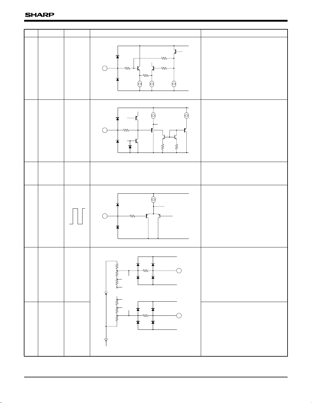
Signal input pin of the ADC.
Connect to the AGCOUT pin via a
capacitor.
This capacitor is also used as the
clamp capacitor of the ADC blank
level clamp.
1.4 V
(Å = L)
ADIN
43
25 µ
VCC4
200
GND4
45
> 2.1 V
< 0.7 V
Pulse input pin of the ADC black
level clamp. Signal is clamped
when low.
When the ADOFS is opened, the
clamped level is set to make the
ADC output 61 (decimal).
Å
45
44
NC
No connection. It is recommended
to connect to GND for better heat
radiation and avoiding noise.
46
V
RT 3.90 V
Upper reference decoupling pin of
the ADC. Connect to the GND
4 via
a capacitor.
VCC4
VRT
GND4
5
VCC4
VRB
GND4
GND4
5
47
46
Lower reference decoupling pin of
the ADC. Connect to the GND
4 via
a capacitor.
1.95 VV
RB
47
 Loading...