


SHARP DV-HR300U Service Manual
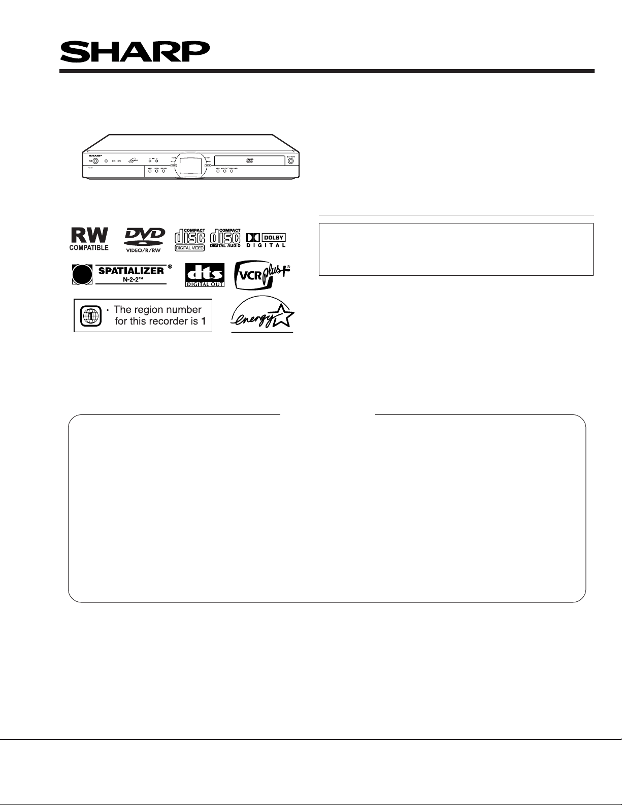
DV-HR300U
SERVICE MANUAL
SX3L5DV-HR300
DVD VIDEO RECORDER
MODEL
In the interests of user-safety (Required by safety regulations
in some countries) the set should be restored to its original
condition and only parts identical to those specified be used.
DV -HR300U
CONTENTS
Page
1. IMPORTANT SERVICE NOTES........................................................................................................ 2
2. FEATURES........................................................................................................................................ 6
3. SPECIFICATIONS ............................................................................................................................. 7
4. PART NAMES.................................................................................................................................... 9
5. DISASSEMBLY METHOD ............................................................................................................... 11
6. TROUBLESHOOTING..................................................................................................................... 15
7. BLOCK DIAGRAMS......................................................................................................................... 26
8. SCHEMATIC DIAGRAMS................................................................................................................ 34
9. PRINTED WIRING BOARD ASSEMBLIES ..................................................................................... 60
10. REPLACEMENT PARTS LIST / EXPLODED VIEWS ..................................................................... 75
11. PACKING OF THE SET................................................................................................................... 95
SHARP CORPORATION
This document has been published to be used for
after sales service only.
The contents are subject to change without notice.
DV-HR300U
1. IMPORTANT SERVICE NOTES
Note:
This unit can be used only where the power
supply is AC 110V-240V, 50/60Hz.
It cannot be used elsewhere.
CAUTION:
USE OF CONTROLS OR ADJUSTMENTS OR
PERFORMANCE OF PROCEDURES OTHER
THAN THOSE SPECIFIED HEREIN MAY RESULT
IN HAZARDOUS RADIATION EXPOSURE.
DO NOT STARE INTO THE LASER BEAM OR
VIEW WITH OPTICAL INSTRUMENT.
WARNING:
TO REDUCE THE RISK OF FIRE OR ELECTRIC
SHOCK, DO NOT EXPOSE THIS EQUIPMENT TO
RAIN OR MOISTURE.
TO REDUCE THE RISK OF FIRE OR ELECTRIC
SHOCK, AND ANNOYING INTERFERENCE, USE
THE RECOMMENDED ACCESSORIES ONLY.
Laser Diode Properties
Material: AlGaInP
Wave length: 650 nm
Emission Duration: Continuous
Laser output: Max. 0.7 mW
Power Cord Protection
To avoid any malfunctions of the unit, and to protect
against electric shock, fire or personal injury, please
observe the following.
Hold the plug firmly when connecting or
disconnecting the AC power cord.
Keep the AC power cord away from heating
appliances.
Never put any heavy object on the AC power cord.
Do not attempt to repair or reconstruct the AC
power cord in any way.
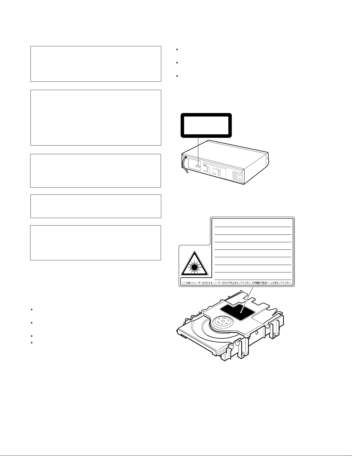
This Unit is classified as a CLASS 1 LASER
product.
The CLASS 1 LASER PRODUCT label is located
on the rear cover.
This product contains a low power laser device.
To ensure continued safety do not remove any
cover or attempt to gain access to the inside of
the product. Refer all servicing to qualified
personnel.
CLASS III
CLASS 1
LASER PRODUCT
LASER PRODUCT
(Rear of product)
(Rear of product)
CAUTION-LASER RADIATION WHEN OPEN. DO NOT STARE INTO BEAM
OR VIEW DIRECTLY WITH OPTICAL INSTRUMENTS.
VORSICHT-LASERSTRAHLUNG, WENN GEFFNET. BLICKEN SIE NICHT IN DEN STRAHL
UND BETRACHTEN SIE DIESEN NICHT DIREKT MIT OPTISCHEN INSTRUMENTEN.
ATTENTION-RADIATION LASER EN CAS D'OUVERTURE. NE PAS FIXER LE
FAISCEAU NI REGARDER DIRECTEMENT DES INSTRUMENTS OPTIQUES.
VARNING-LASERSTRÅLNING NÄR DENNA DEL ÄR ÖPPNAD. STIRRA EJ IN
SA005WJ
I STRÅLEN OCH BETRAKTA EJ STRÅLEN MED OPTISKA INSTRUMENT.
VARO ! AVATTAESSA OLET ALTTIINA LASERSÄTEILYLLE. ÄLÄ TUIJOTA
SÄTEESEEN ÄLÄKÄ KATSO SITÄ OPTISEN LAITTEEN LAPI.
VARNING-LASERSTRÅLNING NÄR DENNA DEL ÄR ÖPPNAD. STIRRA EJ IN I
STRÅLEN OCH BETRAKTA EJ STRÅLEN GEMON OPTISKT INSTRUMENT.
ADVARSEL-LASERSTRÅLING NÅR DEKSEL ÅPNES. STIRR IKKE INN I
STRÅLEN ELLER SE DIREKTE MED OPTISKE INSTRUMENTER.
ADVARSEL-LASERSTRÅLING VED ÅBNING. SE IKKE IND I STRÅLEN-
HELLER IKKE MED OPTISKE INSTRUMENTER.
VARO! AVATTAESSA OLET ALTTIINA LASERSÄTEILYLLE.
ÄLÄ TUIJOTA SÄTEESEEN ÄLÄKÄ KATSO SITÄ OPTISEN LAITTEEN LÄPI.
VARNING - LASERSTRÅLNING NÄR DENNA DEL ÄR ÖPPNAD.
STIRRA EJ IN STRÅLEN OCH BETRAKTA EJ STRÅLEN GENOM OPTISKT
INSTRUMENT.
2
IMPORTANT SERVICE NOTES
DV-HR300U
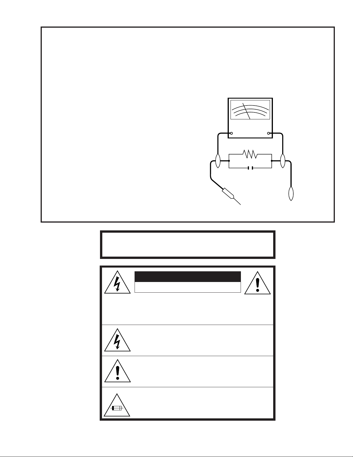
BEFORE RETURNING THE VCR/DVD COMBINATION MODEL
Before returning the video cassette recorder to the user,
perform the following safety checks.
1. Inspect all lead dress to make certain that leads are
not pinched or that hardware is not lodged between
the chassis and other metal parts in the VCR/DVD
combination model.
2. Inspect all protective devices such as non-metallic
control knobs, insulation materials, cabinet backs,
adjustment and compartment covers or shields, isolation resistor/capacitor networks, mechanical insulators etc.
3. To be sure that no shock hazard exists, check for
current in the following manner.
● Plug the AC line cord directly into a 120 volt AC outlet
(Do not use an isolation transformer for this test).
● Using two clip leads, connect a 1.5k ohm, 10 watt
resistor paralleled by a 0.15µF capacitor in series with
all exposed metal cabinet parts and a known earth
ground, such as a water pipe or conduit.
● Use an SSVM or VOM with 1000 ohm per volt, or
higher, sensitivity or measure the AC voltage drop
across the resistor (See Diagram).
● Move the resistor connection to earth exposed metal
part having a return path to the chassis (antenna,
metal cabinet, screw heads, knobs and control shafts,
etc.) and measure the AC voltage drop across the
resistor. Reverse the AC plug on the set and repeat
AC voltage measurements for each exposed part.
Any reading of 0.45V rms (this corresponds to 0.3mA
rms AC.) or more is excessive and indicates a potential shock hazard which must be corrected before
returning the VCR/DVD combination model to the
owner.
SSVM
AC SCALE
1.5k ohms.
10W
0.15 µF
TEST PROBE
TO EXPOSED
METAL PARTS
CONNECT TO
KNOWN EARTH
GROUND
WARNING :TO REDUCE THE RISK OF FIRE OR ELEC-
TRIC SHOCK, DO NOT EXPOSE THIS APPLIANCE TO RAIN OR MOISTURE.
CAUTION
RISK OF ELECTRIC SHOCK
DO NOT OPEN
CAUTION: TO REDUCE THE RISK OF ELECTRIC SHOCK. DO
CAUTION:
3.0A 125V
NOT REMOVE COVER. NO USER-SERVICEABLE
PARTS INSIDE. REFER SERVICING TO QUALIFIED
SERVICE PERSONNEL.
This symbol warns the user of uninsulated voltage
within the unit that can cause dangerous electric shocks.
This symbol alerts the user that there are important
operating and maintenance instructions in the literature
accompanying this unit.
This symbol mark means fast operating fuse.
For continued protection against risk of fire, replace
only with same type fuse F901 (3.0A, 125V).
3
DV-HR300U
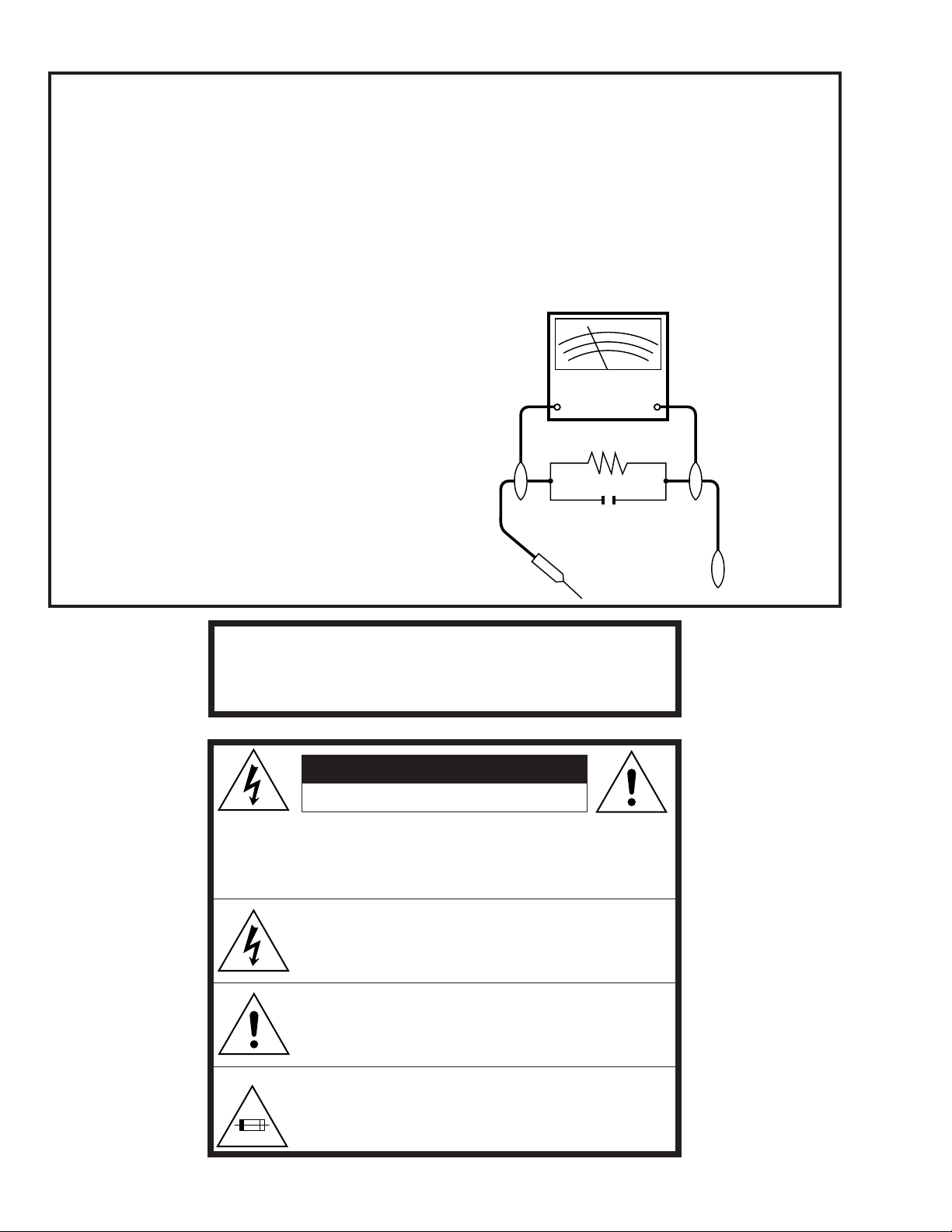
NOTES DE SERVICE IMPORTANTES
AVANT DE RENDRE LE VCR/DVD MAGNETOSCOPE
Avant de rendre le magnétoscope à l’utilisateur, effectuer
les vérifications de sécurité suivantes.
1. Vérifier toutes les gaines de fil pour être sûr que les fils
ne sont pas pincés ou que le matériel n’est pas coincé
entre le châssis et les autres pièces métalliques dans
le VCR/DVD magnétoscope.
2. Vérifier tous les dispositifs de protection tels que les
boutons de commande non métalliques, les matériaux
d’isolement, le dos du coffret, les couvercles de
compartiment et ajustement ou les boucliers, les
réseaux de résistance / condensateur d’isolement, Ies
isolateurs mécaniques, etc.
3. Pour être sûr qu’il n’y a aucun risque de choc électrique,
vérifier le courant de fuite de la maniére suivante.
● Brancher le cordon d’alimentation secteur directement
dans une prise de courant de 120 volts. (Ne pas utiliser
de transformateur d’isolement pour cet essai).
● Utiliser deux fils à pinces et connecter une résistance
de 10 watts 1,5 kohm en parallèle avec un condensateur
de 0,15 µF en série avec des pièces du coffret
métallique exposées et une masse de terre connue
telle qu’un tuyau ou un conduit d’eau.
● Utiliser un VTVM ou VOM avec une sensibilité de 1000
ohms par volt ou plus ou mesurer la chute de tension
CA entre la résistance (voir diagramme).
● Déposer la connexion de la résistance à toutes les
pièces métalliques exposées ayant un parcours de
retour au châssis (connexions d’antenne, coffret
métallique, tétes de vis, boutons et arbres de
commande, etc.) et mesurer la chute de tension CA
entre la résistance. Inverser la fiche CA (une fiche
intermédiaire non polarisée doit être utilisée à seule fin
de faire ces vérifications.) sur l’appareil et répéter les
mesures de tension CA pour chaque piéce métallique
exposée. Toute lecture de 0,45 Vrms (ceci correspond
à 0,3 mArms CA) ou plus est excessive et signale un
danger de choc qui doit être corrigé avant de rendre le
VCR/DVD magnétoscope à son utilisateur.
VTVM
ECHELLE CA
1,5 KOHMS
10W
0,15 µF
SONDE D'ESSAI
VERS PIECES
METALLIQUES
EXPOSEES
CANNECTER A
UNE MASSE DE
TERRE CONNUE
ATTENTION: POUR REDUIRE LES RESQUES D'IN-
CENDIE OU DE CHOC ELECTRIQUE,
NE PAS EXPOSER CET APPAREIL A
LA PLUIE OU A L'HUMIDITE.
ATTENTION
RISQUE DE CHOC ELECTRIQUE
ATTENTION: AFIN DE REDUIRE LES RISQUES DE CHOC
ELECTRIQUE, NE PAS RETIRER LE COUVERCLE,
AUCUN ORGANE INTERNE NE PEUT ETRE
REPARE PAR L'UTILISATEUR. CONFIER
L'APPAREIL A UN DEPANNEUR QUALIFIE.
Ce symbole signale à l'utilisateur la présence d'une
tension non isolée à l'intérieur de l'appareil qui peut être
la cause de secousses électriques dangereuses.
Ce symbole avertit l'utilisateur que des instructions
importantes relatives à l'utilisation et àl'entretien se
trouvent dans le manuel accompagnant l'appareil.
PRECAUTION:
Cette marque indique le fusible à action in stantansée.
Pour la protection continue contre le risque d'incendie,
3,0A 125V
ne remplacer que par le fusible type F901 (3,0A, 125V).
NE PAS OUVRIR
4
DV-HR300U
Precautions for using lead-free solder
1 Employing lead-free solder
"Operation (R) PWB, Operation (L) PWB, Power PWB and UV PWB" of this model employs lead-free solder. The LF
symbol indicates lead-free solder, and is attached on the PWBs and service manuals. The alphabetical character
following LF shows the type of lead-free solder.
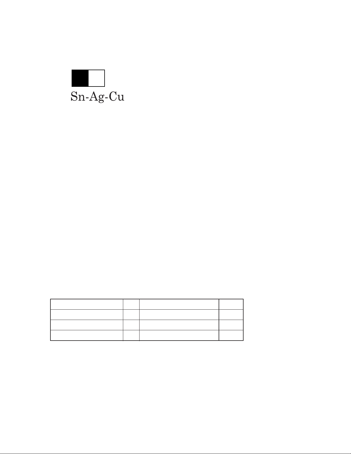
Example:
L Fa
Indicates lead-free solder of tin, silver and copper.
2 Using lead-free wire solder
When fixing the PWB soldered with the lead-free solder, apply lead-free wire solder. Repairing with conventional
lead wire solder may cause damage or accident due to cracks.
As the melting point of lead-free solder (Sn-Ag-Cu) is higher than the lead wire solder by 40°C, we recommend you
to use a dedicated soldering bit, if you are not familiar with how to obtain lead-free wire solder or soldening bit,
contact our service station or service ranch in your area.
3 Soldering
As the melting point of lead-free solder (Sn-Ag-Cu) is about 220°C which is higher than the conventional lead solder
by 40°C, and as it has poor solder wettabillty, you may be apt to keep the soldering bit in contact with the PWB for
extended period of time. However, Since the land may be peeled off or the maximum heat-resistance temperature
of parts may be excoeded, remove the bit from the PWB as soon as you conurm the steady soldering condition.
Lead-free solder contains more tin, and the end of the soldering bit may be easily corroded. Make sure to tum on
and off the power of the bit as required.
if a different type of solder stays on the tip of the soldering bit, it is alloyed with lead-free solder. Clean the bit after
every use of it.
When the tip of the soldering bit is blackened during use, file it with steel wool or fine sandpaper.
Becareful when replacing parts with polarity indication on the PWB silk.
Lead-free wire solder for servicing
Part No. ★ Description Code
ZHNDAi123250E J φ0.3mm 250g(1roll) BL
ZHNDAi126500E J φ0.6mm 500g(1roll) BK
ZHNDAi12801KE J φ1.0mm 1kg(1roll) BM
5
DV-HR300U
2. FEATURES
zz
z A new timer recording system:"Easy Recording
zz
Guide"
» The Recorder is equipped with a high-capacity hard disc, so
you'll have more chances than ever before for timer recording,
and the new timer recording system makes this even easier.
A schedule grid of times and channels is displayed on the
screen, and by simply designating cells in the grid with the
remote control, timer programming becomes as easy as
circling your favorite shows in the newspaper. You can also
see at a glance which time slots are already programmed,
and avoid any overlap.
xx
x High-capacity hard disc lets you record and view
xx
series and your favorite programs
*1
» For trendy dramas, series and other shows you want to watch
and record, without missing a week, use the "Stored Series
Program Timer" feature.
For news and information programs which you watch
everyday and don't need to store, set "Overwrite Program
Timer".
» Recorded programs can be viewed by simply calling them
up with the remote control, so there is no need to search
through a lot of programs.
Programs recorded with "Stored Series Program Timer" can
be batch dubbed onto DVD
*2
, so you can easily save your
favorite dramas on DVD.
*1
This function is only available with hard disc.
*2
Up to 5 titles can be dubbed in a batch.
cc
c DVD-RW/-R recording/playback with outstanding
cc
compatibility
» This Recorder is compatible with digital recording on
rewritable DVD-RW discs and one-time recordable DVD-R
discs. It has two recording formats:
"VR (Video Recording) mode" which has a wealth of editing
functions, and "Video mode" which can be played back with
existing DVD players. This lets you enjoy recording and
dubbing to suit your purpose.
2X or DVD-R Ver. 2.0/4X.
2 Rate conversion dubbing
The mode can be selected from 32 levels just like recording mode.
This enables recording at the optimal picture quality, given the
remaining empty space on the disc.
3 Exact dubbing
This automatically adjusts to the optimal record mode so that
the material is dubbed exactly into the remaining area on the
disc.
The time normally required for a program of an hour on High
Speed Dubbing to a double speed compatible disc
Recording Mode
FINE
SP
LP
EP
nn
n "Time Shift Viewing", "Chasing Playback" and
nn
Speed
Approx. 2✕
Approx. 4✕
Approx. 8✕
Approx. 12✕
Time Required
Approx. 30 min
Approx. 15 min
Approx. 7.5 min
Approx. 5 min
"Simultaneous Recording/Playback" —functions
you can only get with a hard disc
1 Time shift viewing
While you are watching a program, the phone rings.... At times
like this, you can pause the program being broadcast by
pressing a button, and then watch the rest of the program at
your leisure after you finish your phone call. You can also
switch to the current broadcast scene just by pressing
STOP/LIVE button.
2 Chasing playback
You return home earlier than expected while timer recording
is in progress.... At times like this, you don't have to wait for
recording to end. You can immediately view the program from
the beginning.
3 Simultaneous recording/playback
Even while recording to the hard disc, you can enjoy playback
of a DVD, or programs already recorded on hard disc.
You don"t have to wait for recording to finish.
vv
v High picture quality design (Used in all hard disc
vv
and DVD modes)
1 Progressive scanning playback
High-quality, high-density video with no jagged contours and
no flicker.
2 VBR (Variable Bit Rate) recording
Constantly maintains optimal high picture quality by varying
the bit rate (amount of video data) for each scene depending
on the video content (e.g. whether movement is fast or slow).
bb
b A variety of hard disc
bb
1 High speed dubbing
Enables high speed dubbing from hard disc to DVD so you can enjoy
creating your own video library.
*3For high speed dubbing, use discs conforming to DVDRW Ver. 1.1/
↔↔
↔ DVD dubbing functions
↔↔
*3
mm
m Comprehensive editing functions
mm
(Only titles recorded on the hard disc or in VR mode on
DVD-RW can be edited.)
1 Play list edit
This lets you gather only the needed parts (i.e. a "Play List")
from a recorded original video (title).
You can rearrange scenes and combine them with other
scenes, or rearrange titles. This is convenient when you want
to dub and save only the necessary scenes and titles.
2 Chapter edit
This lets you divide a title into chapter units during recording/
playback or using the edit screen. After dividing, a list of
recordings (thumbnails) can be displayed in chapter units,
so you can copy, erase or dub to the play list in chapter units.
3 Scene erase
This lets you erase unnecessary scenes. This is convenient
when you want to cut out the commercials in a recorded
program before dubbing.
6

DV-HR300U
4 Batch erasing of titles/chapters
Titles and chapters which become unnecessary after editing
can be batch erased by selecting them from the list of
recordings (thumbnails).
5 Edit undo function
If you mistakenly erase data during editing, this function lets
you restore it to its immediately preceding state, just like
"Undo" on a PC, so you can edit worry-free.
*4
Edit undo can only be used once. It only works when
"DELETEDIT" is assigned to a colored button (green)
displayed on the screen.
,,
, Simple operation and userfriendly design using a
,,
*4
new remote control
1 START MENU
Press START MENU button on the remote control, and
display the list of main functions on the screen.
After that, you can operate by using the Cursor buttons and
SET/ENTER button on the remote control, so this Recorder
can be used easily even by a person who is unfamiliar with
operation.
2 Colored buttons
The remote control has colored buttons with four different
colors. Functions are displayed in four different colors on the
screen, and the Recorder can be operated by directly
designating these functions.
3 Luminous buttons
Luminous buttons are used for key control buttons on the
remote control so they are easy to see in the dark.
..
. Digital connection (i.LINK) with a digital video/audio
..
source equipment
» The DV IN terminal allows you to uptake, edit and store
material from a digital camcorder equipped with a DV terminal.
//
/ MP3 file playback
//
» This Recorder allows you to playback MP3 files recorded on
CD-RW/R.
ZZ
Z VCR Plus+*5 System
ZZ
» The VCR Plus+ System allows you to program your Recorder
for timer recording simply by inputting the PlusCode
Programming number. The PlusCode numbers are listed in
most newspapers, television guides, and local CATV listings.
Simply by inputting this PlusCode number, you can program
your Recorder for timer recording, eliminating the need to
input program start time, stop time, channel, date and other
information which is necessary for ordinary timer
programming.
*5
VCR Plus+ and PlusCode are registered trademarks of
Gemstar Development Corporation. The VCR Plus+ System
is manufactured under license from Gemstar Development
Corporation.
3. SPECIFICATIONS
General
HDD capacity: 80 GB
Power supply: AC 120 V, 60 Hz
Power consumption (Normal): 40 W
Power consumption (Standby): 0.7 W
Dimensions: Approx. 430 mm x 59 mm x 323 mm (W x H x D)
Approx. 16 15/16" x 22 1/64" x 12 23/32"
Weight: Approx. 5.0 kg (11.1 lbs)
Operating temperature 41°F to 95°F (5°C to 35°C)
Storage temperature: –4°F to 131°F (–20°C to 55°C)
Operating humidity: 10% to 80% (no condensation)
TV systems: NTSC system, 525 lines, 60 fields
Recording
Recordable disc media: DVD-RW, DVD-R
Recording system (HDD): Video: MPEG
Audio: Dolby Digital (2ch)/Linear PCM (FINE mode only)
Recording system (DVD-RW/R): Video: DVD-Video Recording (VR mode)
DVD-VIDEO (Video mode)
Audio: Dolby Digital (2ch)/Linear PCM (FINE mode only)
Recording time (Hard disc): FINE (High picture quality): Approx. 20 hours
SP (Standard): Approx. 33 hours
LP (2X): Approx. 67 hours
EP (3X): Approx. 100 hours
MN (Manual): 32 levels between FINE and EP
(However, the maximum continuous recording time is 12 hours.)
Recording time
(With 4.7GB DVD-RW/R): FINE (High picture quality): Approx. 1 hour
SP (Standard): Approx. 2 hours
7

DV-HR300U
LP (2X): Approx. 4 hours
EP (3X): Approx. 6 hours
MN (Manual): 32 levels between FINE and EP
Playback
Playable discs: DVD Video, DVD-R/RW, Audio CD (CD-DA), Video CD, CD-R/ RW (CD-DA,
Video CD format, MP3 file format)
Tuner
Channel coverage: VHF 2-13
UHF 14-69
CATV 1-125
Timer
Programs: 32 programs/1 year
Clock: Quartz lock (12-hour digital display)
Memory backup: Approx. 1 hour
Input/Output
VHF/UHF antenna input/
output terminal: 75Ω (F-shape connector)
Video input: Input 1, 2 (rear), 3 (front)
Input level: 1 Vp-p (75Ω)
Jacks: RCA jack
Video output:
Output level: 1 Vp-p (75Ω)
Jacks: RCA jack
S-Video input: Input 1, 2 (rear), 3 (front)
Y-Input level: 1 Vp-p (75Ω)
C-Input level: 0.286 Vp-p (75Ω)
Jacks: 4 pin mini DIN
S-Video output:
Y-Output level: 1 Vp-p (75Ω)
C-Output level: 0.286 Vp-p (75Ω)
Jacks: 4 pin mini DIN
Component video output:
Output level: Y: 1 Vp-p (75Ω)
PB, PR: 0.7 Vp-p (75Ω)
Jacks: RCA jack
Audio input: Input 1, 2 (rear), 3 (front) L/R
Input level: 2 V rms (Input impedance: more than 22 kΩ)
Jacks: RCA jack
Audio output: L/R
Input level: 2 V rms (Output impedance: less than 1.5 kΩ)
Jack: RCA jack
Digital audio optical output:
Terminal: Square Optical terminal
DV input:
Terminal: 4 pin (i.LINK/IEEE 1394 standard)
LASER Specification
Wave length: DVD: 658 nm
Laser power: DVD: 100 mW
Specifications are subject to change without notice.
CD: 784 nm
CD: 225 mW
8
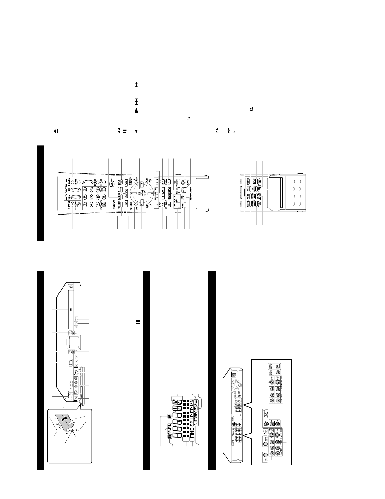
4. PART NAMES
1
2
6
8
10
15
16
121314
17
11
9
7
5
4
3
18
1920212223
24
25
26
28
3130323334
35
29
27
Remote Control Unit
4040
4036
4137
4238
4339
44
1
POWER
2
OPEN/CLOSE
3
Number buttons
4
CH DISPLAY 5TIME SHIFT
6
START MENU7HDD
8
REC LIST/DVD TITLE9Cursor buttons (' /"/\ /|)10EXIT11COLOR BUTTON
Blue (A), Red (B), Green (C), Yellow (D)
12
REV
13
STILL/PAUSE
14
■ STOP/LIVE
15
F.ADV ,
SKIP
16
ÆÆ
ÆÆ
Æ REC
17
REC STOP18TV CONTROL buttons
19
CH " /'20DIRECT21VCR PLUS+
22
DUBBING23P IN P24INPUT/ Repeat25DVD26ORIGINAL/PLAY LIST / DVD MENU
27
SET/ENTER
28
RETURN
29
| PLAY
30
FWD
31
SLOW
32
REPLAY 33SKIP SEARCH
34
REC MODE/
ZOOM
35
REC PAUSE36ANGLE37FUNCTION
38
FAVORITE PROG. LIST/AV AUTO REC39CHAPTER MARK / CONNECTION GUIDE/RESET
40
AUDIO41SUBTITLE
42
DISPLAY/BACKLIGHT
43
ON SCREEN
44
TAMPER PROOF
Main Unit (Front)
Front Panel Display
1
9
10 11 12 1314 15 16 17 18 19
23
4 5 6
8
7
To open the
front door, lay
your finger on
this part and pull
toward you.
1
456
7
8
9
3
2
Main Unit (Rear)
1
45
2 3
7 8
6
9
1
POWER 2STANDBY indicator
3
TIMER indicator
4
CHANNEL "/'5PLAY/REC indicators
(for HDD)
6
PLAY/REC indicators
(for DVD)
7
Disc tray
8
OPEN/CLOSE
9
RESET10LINE IN 3
• AUDIO Input jacks
• VIDEO Input jack
• S-VIDEO Input jack
11
DV IN terminal
12
●
REC
13
REC STOP14REC PAUSE15HDD
16
DVD
17
|
PLAY
18
■ STOP/LIVE
19
STILL/PAUSE
1
Chapter indicator
2
Disc Remaining Time indicator
3
Title indicator
4
Dubbing indicator
5
Recording Mode indicator
6
AV AUTO REC indicator
7
Information Display
8
Tamper Proof indicator
9
Simple Recording Timer indicator
1
PASS THROUGH jack2IN FROM ANTENNA jack (antenna or cable
input)3COMPONENT Video Output jacks
4
LINE IN 1 (AUTO REC)
• AUDIO Input jacks
• VIDEO Input jack
• S-VIDEO Input jack
5
LINE IN 2
• AUDIO Input jacks
• VIDEO Input jack
• S-VIDEO Input jack
6
LINE OUT 1
• AUDIO Output jacks
• VIDEO Output jack
• S-VIDEO Output jack
7
LINE OUT 2
• AUDIO Output jacks
• VIDEO Output jack
• S-VIDEO Output jack
8
DIGITAL AUDIO Output COAXIAL jack9DIGITAL AUDIO Output OPTICAL terminal
DV-HR300U
9
DV-HR300U
1
While pressing down,
slide the battery cover in
the direction of the
arrow.
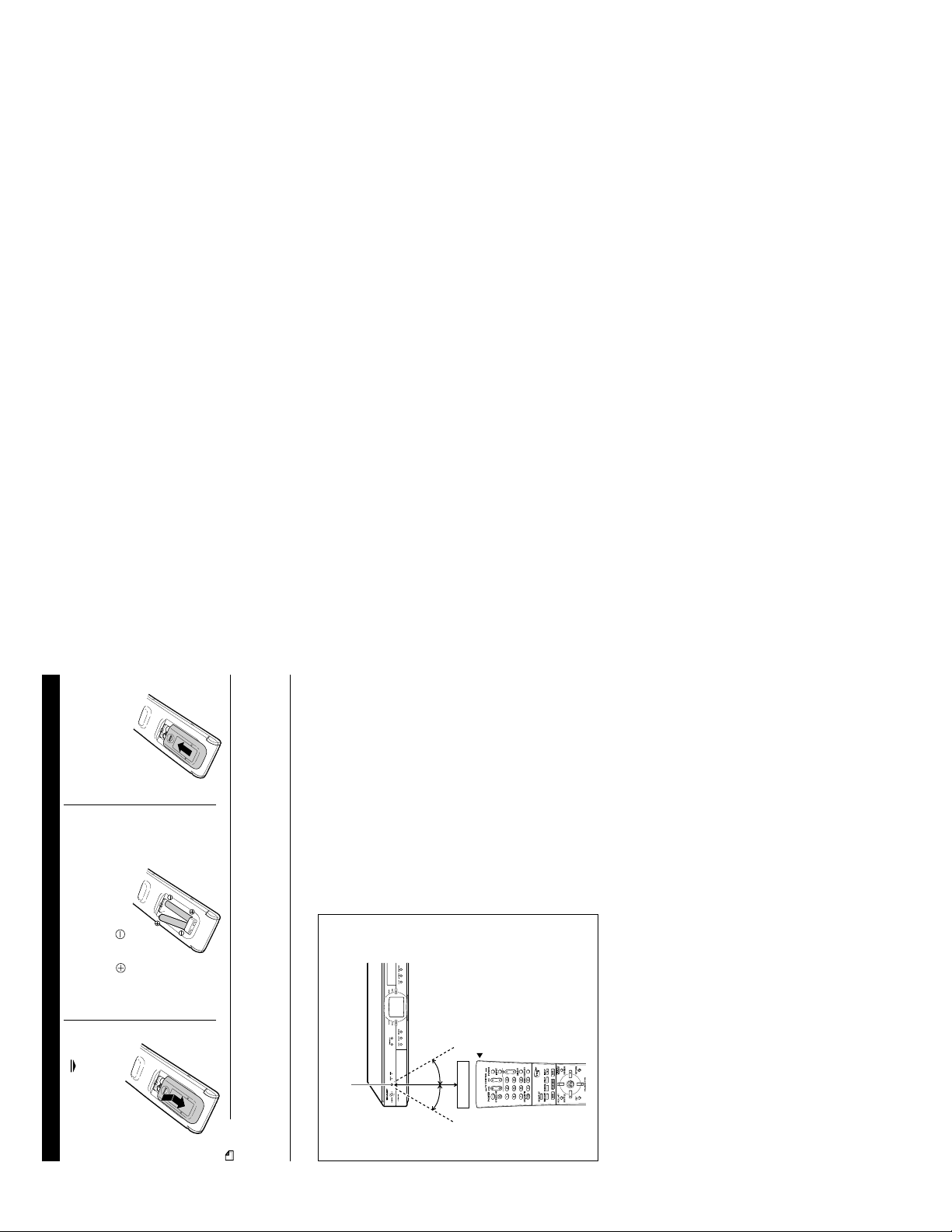
2
Load the batteries.
Load the two “AAA” size batteries (R-03,
UM/SUM-4) supplied with the remote
control unit. Make sure that the battery
poles
and
are positioned as
indicated.
3
Slide the battery cover
in the direction of the
arrow until it clicks.
About 30ϒ
About 30ϒ
Front 22.96ft.
Remote control
unit
Operating range of remote control
NOTE
» Do not subject the remote control unit to shock, water or excessive humidity.
» The remote control unit may not function if the Recorder s remote sensor is in direct sunlight or any other strong light.
» Incorrect use of batteries may cause them to leak or burst. Read the battery wa rnings and use the batteries properly.
» Do not mix old and new batteries, or mix dif ferent brands.
» Remove the batteries if you will not use the remote control unit for an extended period of time .
Loading the Batteries
Remote sensor
10
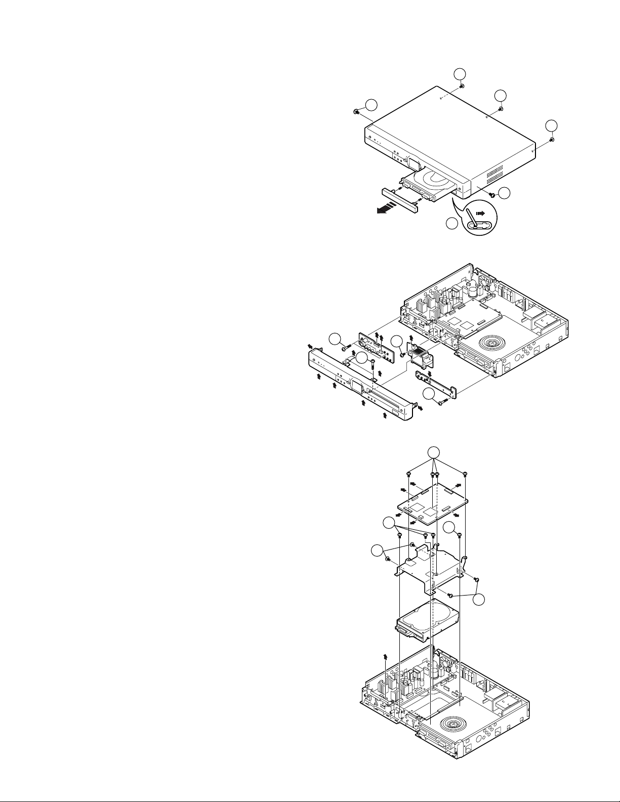
5. DISASSEMBLY METHOD
DV-HR300U
5-1. DISASSEMBLY METHOD
(1) Removing the top cabinet
1.Remove five screws 1.
2.Slide back the top cabinet by 10 mm and remove upward.
(2) Removing the panel
1. Push a protruding part shown in a at the bottom with a
screwdriver, etc.
2.Remove the tray decoration assembly (detach springs from
four claws on the backside of the tray).
3.Remove two screws 2 and spring.
4.Pull the panel to remove as detaching from the eight claws.
(3) Removing the operation PWB and LCD PWB
1.Remove the FFC and four harnesses.
2.Remove two screws 3, a screw 4 and a screw 5.
3.Pull each PWB to remove.
1
1
a
3
2
5
1
1
1
(4) Removing the main PWB
1.Remove four screws 6.
2.Remove the FFC and six harnesses.
3.Remove the main PWB upward.
(5) Removing the HDD unit
1.Remove four screws 7.
2.Remove the HDD unit (with the angle) upward.
3.Remove four screws 8.
4.Remove the HDD unit.
5.Disconnect the flat cable and power cable.
4
6
7
8
7
8
11
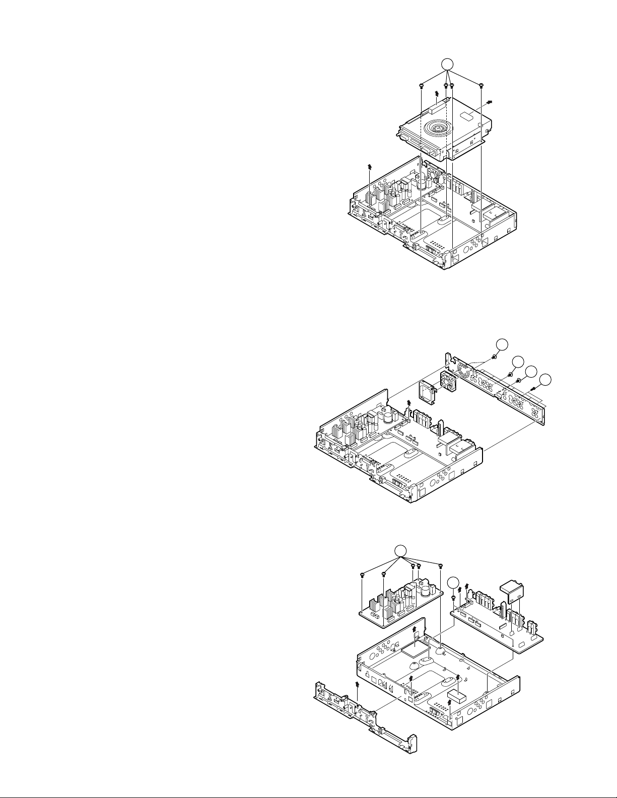
DV-HR300U
(6) Removing the DVD unit
1.Remove four screws 9.
2.Remove the DVD unit (with the angle) upward.
3.Disconnect cables including the flat cable and power cable.
4.Remove the gasket.
(7) Removing the rear terminal board and fan
1.Detach the fan cable from the main unit.
2.Remove two screws 0.
3.Detach the fan and fan cover.
4.Remove a screw q, two screws (tuner) w and eight screws e
(terminals)
5.Pull the rear terminal board backward to remove.
9
10
13
11
12
(8) Removing the UV PWB, BS PWB, power PWB and terminal PWB
1.Remove UV PWB upward.
2.Disconnect the connection cables from the power PWB and terminal PWB.
3.Remove five screws r.
4.Remove the power PWB upward.
5.Remove two screws t.
6.Remove the terminal PWB upward.
7. Remove two hooks and the PWB holder in the direction of the
arrow.
8.Remove one insulation sheet and three gasket.
12
14
15
5-2. EXTENSION CABLE DIAGRAM
Parts Code Price Code Parts name / Use
1 QCNW-C072WJZZ AD Main to Sub Signal Line CN3001—S2202
2 QCNW-C073WJZZ AD Main to Sub Control Line CN3003↔S2201
3 QCNW-C074WJZZ AT Main to Power CN3004↔P9005
4 QCNW-B712WJZZ AH ATAPI cable for HDD CN4502↔ATAPi
DV-HR300U
1
2
25pin
21pin
POWER Unit
Sub PWB
12pin 12pin
3
40pin
4
Development for repair
Extension with QCNW-C072WJZZ
1
HDD Unit
Extension with
3
QCNW-C074WJZZ
Extension with
4
QCNW-B712WJZZ
Main PWB
Extension with
2
QCNW-C073WJZZ
13
DVD RW Unit

DV-HR300U
5-3. Notes for servicing
1. After replacing the HDD or main PWB, register the HDD-ID again.
2. After replacing I54R NOR flash (IC7502) or NAND flash (IC7509), upgrade the version using the CD.
All the data in the HDD will be formatted by replacing the main PWB unit.
The following parts cannot be replaced as the system information needs to be written. (Replace the PWB.)
1. EEPROM for I54R, IC7507 and IC7508
Setting procedure after replacement of HDD or main PWB
1) HDD installation
The unit can be started after installing the HDD, but key operation is impossible since the HDD-ID is not registered.
Perform HDD aging to register the HDD-ID.
2) HDD aging
The test mode can be accessed after replacing the HDD.
[1] Enter the test mode with the keys on the main unit (press the channel UP key and recording stop key simulta-
neously).
[2] Enter “4” to open the drive screen.
[3] Press the play key to enter the HDD aging mode.
“0” appears on the LCD of the front panel. It increases to 58 and then changes to “777” when the aging is
completed.
Should “EEE” appear, replace the HDD and start the process over. Aging takes approx. 2.5 hours.
[4] The aging is completed when “777” appears, and the HDD-ID is registered automatically.
If the main PWB unit is replaced, enter the test mode and press the “10/0” key on the remote control to register
the HDD-ID.
[5] Restart the unit and check the operation.
3) Factory setting
Initialize all the settings. Enter the test mode and press the “11” key on the remote control. The display stays black
during the initialization process.
Initialization is completed when the test mode appears on the LCD display following “507”.
Note: The descriptions in red are temporary (as of September 2, 2003) and subject to change.
5-4. Writing of software
1. Press the power key to turn on the power.
2. Open the tray with the tray open/close key and place the version upgrade CD.
3. Close the tray. Upgrade begins automatically.
“200” appears on the main unit display.
4. When the upgrade finishes, the tray opens and “208” appears on the main unit display.
5. Turn off the power to complete the upgrade.
• Upgrade the writer in the same way. In this case, “300” and “307” appear on the main unit display during the process.
14
DV-HR300U
FLOW CHART No.1
With power on, circuits on main PWB do not work properly.
Power turns off approx. 5 seconds after turned on.
NO
NO
Are voltages of 3.3V (VDDP3.3, VDDADC3.3,
VDDP_A3.3) and 1.8V (VDDC1.8) applied to
pins of IC7506?
After power on, is 154_RS signal ("H" → "L"
when reset) input to IC7506 pin 257?
YES
Reset
Check
Is IC7506 pin 279 BOOTSEL1 at "L" level and
pin 278 BOOSTSEL0 at "H" level?
YES
With power on, is data input to IC7506 pins 81,
82, 86, 87, 91-94, 96-98, 101-104 and 108
(RAMDAT [31:16])?
YES
Is serial communication established between
IC7506 and sub unit IC501?
IC7506 pin 34 FPCDOUT (SUBMIC_D_OUT)
IC7506 pin 36 FPCSTB (SUBMIC_CS)
IC7506 pin 38 FPCCLK (SUBMIC_CLK)
IC7506 pin 39 FPCDIN (SUBMIC_D_IN)
YES
NO
NO
NO
NO
NO
Is reset signal ("H" → "L" when reset) input to
pins of each IC?
IC3502 pin 84 YCDEC_RST
IC7304 pin 151 ENCRST
IC4005 pin 1 DV_RST
IC3009 pin 5 DACADC_RST
IC3005 pin 13 AD_RST
NO
With power on, is fan running?
Fan is defective or power supply failure.
Check D_3.3V (1) and 1.8V lines (IC7506).
Check IC4501 and peripheral
circuits.
Check 154_RST line between IC501 pin 98 and
IC7506 pin 257.
Check BOOTSEL1 (DOWN L [H]) line between IC501
pin 22 and IC7506 pin 257 as well as BOOTSEL0 line
between Q7507 collector and IC7506 pin 278.
Check lines between pins of IC7502 and IC7506.
Check lines between pins of IC7506 and sub PWB
IC501.
IC7506 pin 34 ← IC501 pin 16 TU_D_OUT
IC7506 pin 36 → Q532, 533 → IC501 pins 2, 3 TU_CS
IC7506 pin 38 → Q534, 535 → IC501 pin 14 TU_CLK
IC7506 pin 39 → Q536, 537 → IC501 pin 15
MAIN_DATA
YES
With power on, is data input to IC7506 pins 63,
64, 66-69, 73 and 74 NVMDA [7:0]?
After power on, is reset signal ("H" → "L"
when reset) input to IC4501 pin 54?
IC4501 pin 54 SV_RST
YES
NO
Check lines between pins of IC7509 and IC7506.
Check SV_RST line between IC7506 pin 29 and
IC4501 pin 54.
YES
NO
Is 27MHz clock signal input to pins of the
following ICs?
IC7506 pins 252, 256 27MHz_OSC
IC7304 pins 28, 34 MPENC_SCLK
IC4005 pins 50, 202 INVCK4
Check lines between pins of IC4501 and other ICs.
IC4501 pin 113 → IC3502 pin 84 YCDEC_RST
IC4501 pin 139 → IC7304 pin 151 ENCRST
IC4501 pin 78 → IC4005 1 pin DV_RST
IC4501 pin 99 → IC3009 pin 5 DACADC_RST
IC4501 pin 64 → IC3005 pin 13 AD_RST
NO
Check IC7506 and peripheral
circuits.
NO
YES
YES
YES
NO
Check X3001 and peripheral
circuits.
Check IC3004 and peripheral
circuits.
Is 27MHz clock signal output to X3001 pin 4?
NO
Check X3502 and peripheral circuits.
Is 27MHz clock signal to each pin of IC3004?
IC3004 pin 14 27MHz_OSC
IC3004 pin 18 MPENC_SCLK
IC3004 pin 16 INVCK4
Check lines between pins of IC3004 and other ICs.
IC3004 pin 14 → IC7506 pins 252, 256 27MHz_OSC
IC3004 pin 18 → IC7304 pins 28, 34 MPENC_SCLK
IC3004 pin 16 → IC4005 pins 50, 202 INVCK4
NO
YES
NO
Check IC7506 and peripheral
circuits.
NO
YES
YES
YES
Is 27MHz clock signal input to IC4501 pins 18,
91?
IC4501 pins 18, 91 SBCLK
Is 135MHz clock signal PCLK input to IC7510/
7511pin 38?
Is 24.576MHz clock signal output on IC3502
pin 43?
NO
Check IC7506 and peripheral circuits.
Is 135MHz clock signal PCLK output to IC7506 pin
134?
Check SBCLK (RP_SBCLK) line between IC7506
pin 208 and IC4501 pins 18, 91.
Check lines between IC7506 pin 134 and IC7510/
7511 pin 38.
NO
YES
Clock
Check
Clock
Check
After power on, is reset signal ("H" → "L" when reset)
output to IC7506 pin 79?
IC7506 pin 79 SV_RST
1
1
Is reset signal ("H" → "L" when reset) output to each
pin of IC4501?
IC4501 pin 113 YCDEC_RST
IC4501 pin 139 ENCRST
IC4501 pin 78 DV_RST
IC4501 pin 99 DACADC_RST
IC4501 pin 64 AD_RST
NO
Is 27MHz clock signal output to IC7506 pin 208?
IC7506 pin 208 RP_SBCLK
6. TROUBLE SHOOTING
15
DV-HR300U
FLOW CHART No.2
Drive is not working properly (communication failure with IC7506).
Is ATAPI reset released? (CN4501 pin 1 R4537: "H" level)
NO
Check IC7506 and peripheral
circuits.
YES
YES
Check following items.
NO
Check power unit and PC_12V
and PC_5V circuits.
Communicating with drive via ATAPI?
Access drive when CN4501 pin 37 CS0 and pin 38 CS1 are at "L"
level. (Communication is ongoing if intermittently set at LOW.)
CN4501 pin 35 DA0, pin 33 DA1, pin 36 DA2 and ATAPI register
address (Intermittently set at LOW).
CN4501 pin 31 INTRQ is at "H" level when drive interrupts. Output
after processing transfer command from IC7506, etc.
CN4501 pin 21 DMARQ is at "L" level when drive requests data
transfer.
CN4501 pin 29 DMACK is at "L" level when IC7506 receives data
transfer for DMARQ from drive.
When CN4501 pin 25 DIOR and pin 23 DIOW are at "L" level,
IC7506 sends REASD/WRITE to drive. (Communication is ongoing
if CS and DA are intermittently set at LOW.)
Are 12V and 5V applied to drive?
FLOW CHART No.3
HDD is not working properly (communication failure with IC7506).
Is ATAPI reset released? (CN4502 pin 40 R4566: "H" level)
NO
Check IC7506 and peripheral
circuits.
YES
YES
Check following items.
NO
Check power unit and PC_12V
and PC_5V circuits.
Communicating with drive via ATAPI?
Access drive when CN4502 pin 4 CS0 and pin 3 CS1 are at "L"
level. (Communication is ongoing if intermittently set at LOW.)
CN4502 pin 6 DA0, pin 8 DA1, pin 5 DA2 and ATAPI register
address (intermittently set at LOW).
CN4502 pin 10 INTRQ is at "H" level when drive interrupts. Output
after processing transfer command from IC7506, etc.
CN4502 pin 20 DMARQ is at "L" level when drive requests data
transfer.
CN4502 pin 12 DMACK is at "L" level when IC7506 receives data
transfer for DMARQ from drive.
When CN4502 pin 16 DIOR and pin 18 DIOW are at "L" level,
IC7506 sends REASD/WRITE to drive. (Communication is ongoing
if CS and DA are intermittently set at LOW.)
Are 12V and 5V applied to HDD?
Is MPEG2_PS data signal properly connected between pins of
IC7304 and IC4501?
IC7304 pin 66 → IC4501 pin 138 OSSTD (stream data strobe)
IC7304 pins 56-59, 61, 63-65 → IC4501 pins 3-7, 10-12
OS [7:0] (stream data)
IC7304 pin 70 ← IC4501 pin 141 OSREQ ("L" level when
IC4501 requests data transfer.)
IC7304 pin 68 → IC4501 pin 13 OSVLD (stream data valid)
IC7304 pin 67 → IC4501 pin 19 OSSYNC (stream data sync)
FLOW CHART No.4
Recording is impossible (MPEG stream check)
NO
Check IC7304, IC4501 and peripheral
circuits as well as lines between pins of
IC7304 and IC4501.
YES
NO
Check IC4501, IC7506 and peripheral
circuits as well as lines between pins of
IC4501 and IC7506.
Is MPEG2_PS data signal properly connected between pins of
IC4501 and IC7506?
IC4501 pin 18 ← IC7506 pin 208 SBCLK (transfer clock 27MHz)
IC4501 pin 23 → IC7506 pin 240 SBDAT (stream data)
IC4501 pin 22 → IC7506 pin 234 SBVALID ("H" level when
transferred data is valid)
IC4501 pin 21 ← IC7506 pin 213 SBREQ ("H" level when
IC7506 requests data transfer)
IC4501 pin 20 → IC7506 pin 239 SBSOS (sector head signal)
16
DV-HR300U
Y/C/C
B
/C
R
output
Is video signal output to each pin of IC7506?
IC7506 pin 218 (R7742) Y OUT (Q7506 pin 5 B)
IC7506 pin 214 (R7744) C OUT (Q7505 pin 5 B)
IC7506 pin 245 (R7724) C
B
(B_U) OUT (Q7503 B)
IC7506 pin 224 (R7737) C
R
(R_V) OUT (Q7502 B)
FLOW CHART No.5
Playback video signal is not output from main PWB.
Is drive control of IC7506 working properly?
Is HDD control working properly?
YES
Check lines between pins of IC7506 and CN3001 as well as
circuits on lines.
IC7506 pin 218 (R7742) → Q7506 → Q7509 (FL7501 →
Q7508 in LP mode) → IC7512 → CN3001 pin 23 154_Y
IC7506 pin 214 pin (R7744) → Q7505 → CN3001 pin 25 154_C
IC7506 pin 245 pin (R7724) → Q7503 → CN3001 pin 19 154_B/U
IC7506 pin 224 pin (R7737) → Q7502 → CN3001 pin 20 154_R/V
NO
NO
Refer to Flow chart No.2 "Drive is not working
properly (communication failure with IC7506)"
or Flow chart No.3 "HDD is not working
properly (communication failure with IC7506)".
Check IC7506 and peripheral circuits.
YES
Y/P
B
/P
R
output (progressive mode)
Is video signal output to each pin of IC7506?
IC7506 pin 223 (R7738) Y (G_Y) OUT (Q7501 B)
IC7506 pin 245 (R7724) P
B
(B_U) OUT (Q7503 B)
IC7506 pin 224 (R7737) P
R
(R_V) OUT (Q7502 B)
NO
YES
Check IC7506 and peripheral circuits.
Check lines between pins of IC7506 and CN3001 as well as
circuits on lines.
IC7506 pin 223 pin (R7738) → Q7501 → CN3001 pin 18 154_G/Y
IC7506 pin 245 pin (R7724) → Q7503 → CN3001 pin 19 154_B/U
IC7506 pin 224 pin (R7737) → Q7502 → CN3001 pin 20 154_R/V
Is video signal output to pins of main unit connector CN3001?
CN3001 pin 23 154_Y
CN3001 pin 25 157_C
FLOW CHART No.6
Playback images do not appear properly (from video/S output).
NO
Refer to Flow chart No.5 "Playback video
signal is not output from main PWB".
Check circuits and lines between pins of
main unit connector CN3001 and input pins
of IC2802.
CN3001 pin 23 → S2202 pin 23 → Q2502,
2504, 2507 → IC2802 pin 2 OSD_Y_IN
CN3001 pin 25 → S2202 pin 25 → Q2501,
2503, 2506 → IC2802 pin 4 OSD_C_IN
YES
NO
Check lines between IC2501 pin 21 and
S-OUT 1/2 Y terminals (J2402) as well as
S-OUT 1/2 terminals (J2402).
Check lines between IC2501 pin 26 and
S-OUT 1/2 C terminals (J2402) as well as
S-OUT 1/2 terminals (J2402).
Check lines between IC2501 pin 23 and
VIDEO OUT 1/2 terminals (J2402) as well as
VIDEO OUT 1/2 terminals (J2402).
Is video signal input to each pin of sub unit IC2802?
IC2802 pin 2 OSD_Y_IN
IC2802 pin 4 OSD_C_IN
YES
NO
Is 5V applied to IC2501 pins 1, and 28?
Is 5V applied to IC2802 pin 7?
Is IC2501 pin 3 at "H" level?
Check PC_5V (1) line
Check PC_5V (1)
line.
NO
NO
Is video signal output to each pin of IC2802?
IC2802 pin 8 OSD_Y
IC2802 pin 6 OSD_C
YES
Is video signal input to each pin of IC2501?
IC2501 pin 6 OSD_Y
IC2501 pin 2 OSD_C
YES
Is video signal output to each pin of IC2501?
IC2501 pin 21 Y_OUT
IC2501 pin 26 C_OUT
IC2501 pin 23 V_OUT
Check lines between pins of IC2802 and
IC2501.
IC2802 pin 8 → IC2501 pin 6 OSD_Y
IC2802 pin 6 → IC2501 pin 2 OSD_C
YES
NO
NO
NO
Is video signal output to each output terminal?
SIs Y signal output to S-OUT 1/2 terminals (J2402)?
Is C signal output to S-OUT 1/2 terminals (J2402)?
Is CVBS signal output to VIDEO OUT 1/2 terminals (J2402)?
NO
YES
ICheck or replace
IC2501.
YES
Check or replace
IC2801.
YES
YES
Is T_V_MUTE line
at "L" level?
NO
NO
Check Q2510 and
R2515.
Check T_V_MUTE
line.
NO
17
DV-HR300U
Is video signal output to pins of main unit
connector CN3001?
CN3001 pin 23 154_Y
CN3001 pin 19 154_B/U
CN3001 pin 20 154_R/V
FLOW CHART No.7
Playback images do not appear properly (from Y/C
B
/C
R
output).
NO
Refer to Flow chart No.5 "Playback video signal is not output
from main PWB".
YES
NO
Is video signal input to pins of sub unit IC2802
and 2801?
IC2802 pin 2 OSD_Y_IN
IC2801 pin 1 OSD_PB_IN
IC2801 pin 14 OSD_PR_IN
YES
YES
Is 5V applied to IC2802 pin 7?
Is 5V applied to IC2801 pin 13?
Is video signal input to pins of IC2802 and
2801?
IC2802 pin 8 OSD_Y
IC2801 pin 3 OSD_P
B
IC2801 pin 5 OSD_P
R
YES
NO
NO
NO
Check lines between pins of IC2802 and 2801 and pins of
IC2502.
IC2802 pin 8 → IC2502 pin 8 OSD_Y
IC2801 pin 3 → IC2502 pin 11 OSD_PBIC2801 pin 5 → IC2502 pin 16 OSD_P
R
Is video signal input to each pin of IC2502?
IC2502 pin 8 OSD_Y
IC2502 pin 11 OSD_PBIC2502 pin 16 OSD_P
R
NO
Check or replace
IC2801.
YES
YES
Check or replace
IC2801.
Check PC_5V (1) line.
Check PC_5V (1) line.
NO
Check circuits and lines between pins of main unit connector
CN3001 and input pins of IC2802/2801.
CN3001 pin 23 → S2202 pin 23 → Q2502, 2504, 2507 →
IC2802 pin 2 OSD_Y_IN
CN3001 pin 19 → S2202 pin 19 → Q2512, 2515 →
IC2801 pin 1 OSD_ P
B
_IN
CN3001 pin 20 → S2202 pin 20 → Q2513, 2516 →
IC2801 pin 14 OSD_ P
R
_IN
Check line between IC2501 pin 20 and component Y terminal
(J2403) as well as component terminal (J2403).
Check line between IC2501 pin 18 and component C
B
terminal
(J2403) as well as component terminal (J2403).
Check line between IC2501 pin 16 and component C
R
terminal
(J2403) as well as component terminal (J2403).
Check line between IC2501 pin 20 and DY terminal (CN2401) as
well as component terminal (CN2401).
Check line between IC2501 pin 18 and D C
B
terminal (CN2401)
as well as component terminal (CN2401).
Check line between IC2501 pin 16 and D C
R
terminal (CN2401)
as well as component terminal (CN2401).
YES
NO
Is 5V applied to IC2502 pin 13?
Is IC2502 pin 12 PROGRE (H) line at "L" level?
Check PC_5V (1) line.
Is video signal input to each pin of IC2502?
IC2502 pin 6 COM_Y
IC2502 pin 5 C
B
IC2502 pin 3 C
R
YES
NO
NO
NO
NO
NO
NO
Is video signal output to each output terminal?
Is Y signal output to component terminal
(J2403)?
Is C
B
signal output to component terminal
(J2403)?
Is C
R
signal output to component terminal
(J2403)?
Is Y signal output to D terminal (CN2401)?
Is C
B
signal output to D terminal (CN2401)?
Is C
R
signal output to D terminal (CN2401)?
NO
YES
Check or replace
IC2502.
YES
YES
Check PROGRE (H) line.
NO
Check Q2510 and
R2515.
Check T_V_MUTE line.
NO
NO
Check lines between pins of IC2502 and IC2501.
IC2502 pin 6 -> IC2501 pin 10 COM_Y
IC2502 pin 5 -> IC2502 pin 12 C
B
IC2502 pin 3 -> IC2502 pin 14 C
R
Is video signal input to each pin of IC2501?
IC2501 pin 10 COM_Y
IC2502 pin 12 C
B
IC2502 pin 14 C
R
YES
NO
Is 5V applied to IC2501 pins 1 and 28?
Is IC2501 pin 13 at "H" level?
Check PC_5V (1) line.
Is video signal output to each pin of IC2501?
IC2501 pin 20 COMPO_Y
IC2501 pin 18 C
B
_OUT
IC2501 pin 16 C
R
_OUT
NO
YES
Check or replace
IC2501.
YES
Is T_V_MUTE line at "L" level?
NO
1
1
18
DV-HR300U
Is video signal output to pins of main unit
connector CN3001?
CN3001 pin 18 154_G/Y
CN3001 pin 19 154_B/U
CN3001 pin 20 154_R/V
FLOW CHART No.8
Playback images do not appear properly (from Y/C
B
/C
R
output).
NO
YES
NO
Is video signal input to each pin of IC2502?
IC2502 pin 9 154_Y
IC2502 pin 14 154_P
B
IC2502 pin 1 154_P
R
YES
NO
Is 5V applied to IC2502 pin 13?
Is IC2502 pin 12 PROGRE (H) at "H" level?
Check PC_5V (1) line.
Is video signal input to each pin of IC2502?
IC2502 pin 6 COM_Y
IC2502 pin 5 C
B
IC2502 pin 3 C
R
YES
NO
Check lines between pins of IC2501 and pins of IC2502.
IC2502 pin 6 → IC2501 pin 10 COM_Y
IC2502 pin 5 → IC2501 pin 12 C
B
IC2502 pin 3 → IC2501 pin 14 C
R
Is video signal input to each pin of IC2501?
IC2501 pin 10 COM_Y
IC2501 pin 12 C
B
IC2501 pin 14 C
R
NO
YES
Check or replace
IC2502.
YES
Check PROGRE (H) line.
NO
Check circuits and lines between pins of main unit connector
CN3001 and input pins of IC2502.
CN3001 pin 18 → S2202 pin 18 → Q2511, 2514, 2518 →
IC2502 pin 9 154_Y
CN3001 pin 19 → S2202 pin 19 → Q2512, 2515 →
IC2502 pin 14 154_ P
B
CN3001 pin 20 → S2202 pin 20 → Q2513, 2516 →
IC2502 pin 1 154_ P
R
Check line between IC2501 pin 20 and component Y terminal
(J2403) as well as component terminal (J2403)?
Check line between IC2501 pin 18 and component P
B
terminal
(J2403) as well as component terminal (J2403)?
Check line between IC2501 pin 16 and component P
R
terminal
(J2403) as well as component terminal (J2403)?
Check line between IC2501 pin 20 and DY terminal (CN2401)
as well as D terminal (CN 2401)?
Check line between IC2501 pin 18 and D P
B
terminal (CN2401)
as well as D terminal (CN 2401)?
Check line between IC2501 pin 16 and D P
R
terminal (CN2401)
as well as D terminal (CN 2401)?
YES
NO
Is 5V applied to IC2501 pins 1 and 28?
Is IC2501 pin 13 at "H" level?
Check PC_5V (1) line.
Is video signal output to each pin of IC2501?
IC2501 pin 20 COMPO_Y
IC2501 pin 18 C
B
_OUT
IC2501 pin 16 C
R
_OUT
YES
NO
NO
NO
NO
NO
NO
Is video signal output to each output terminal?
Is Y signal output to component terminal
(J2403)?
Is P
B
signal output to component terminal
(J2403)?
Is P
R
signal output to component terminal
(J2403)?
Is Y signal output to D terminal (CN2401)?
Is P
B
signal output to D terminal (CN2401)?
Is P
R
signal output to D terminal (CN2401)?
NO
YES
Check or replace
IC2501.
YES
YES
Is T_V_MUTE line at "L" level?
NO
Check Q2510 and
R2515.
Check T_V_MUTE line.
NO
Is video signal input to IC2203 pins
1, 8, 15, 23 and 47?
Is luminance signal input to IC 2203
pins 3, 10 and 17?
Is chroma signal input to IC 2202
pins 5, 12 and 19?
FLOW CHART No.9
Image E-E does not appear.
1 In external video input mode
■ Check line between rear video input 1 terminal (J2401) and IC2203 pin 8.
■ Check line between rear video input 2 terminal (J2402) and IC2203 pin 15.
■ Check line between front video input 3 terminal (J2702) and IC2203 pin 1.
2 In external S input mode
■ Check line between rear S Y input 1 terminal (J2401) and IC2203 pin 10.
■ Check line between rear S Y input 2 terminal (J2401) and IC2203 pin 17.
■ Check line between front S Y input 3 terminal (J2701) and IC2203 pin 3.
■ Check line between rear S C input 1 terminal (J2401) and IC2203 pin 12.
■ Check line between rear S C input 2 terminal (J2401) and IC2203 pin 19.
■ Check line between front S C input 3 terminal (J2701) and IC2203 pin 5.
3 In U/V tuner mode
Check line between pin 18 of U/V tuner (TU1501) and IC2203 pin 47.
4 In BS tuner mode
Check line between pin 18 of BS tuner (TU1701) and IC2203 pin 23.
YES
NO
Is video signal input to pins of main unit
connector CN3001?
CN3001 pin 1 CVBS/Y signal
CN3001 pin 3 C signal
NO
In external video input 1/2/3 mode, U/V tuner mode or
BS tuner mode:
Is video signal output to IC2203 pin 43?
Is 9V applied to IC2203 pin 34?
Check or replace IC2203.
Check PC_9V line.
NO
YES
YES
NO
YES
YES
NO
Is signal input to pin 26 PLL_SCL and pin 27 PLL_SDA
controlling IC2203?
Check PLL_SCL and
PLL_SDA lines.
YES
NO
YES
In external S input 1/2/3 mode:
Is luminance signal output to IC2203
pin 43?
Is chroma signal output to IC2203
pin 45?
Are these lines at "L" level: IC501 pin 29 AUX1_S_SOCK (rear
AUX1), pin 64 AUX3_S_SOCK (rear AUX2), and pin 28
F_SJACK (front AUX3)?
NO
Check these lines: AUX1_S_SOCK (rear AUX1),
AUX3_S_SOCK (rear AUX2) and F_SJACK (front
AUX3).
Check circuits and lines between IC2203 pin 43 and CN3001
pin 1 and between IC2203 pin 45 and CN3001 pin 3.
IC2203 pin 43 → Q2207 → S2202 pin 1 → CN3001 pin 1
CVBS/Y signal
IC2203 pin 45 → Q2208 → S2202 pin 3 → CN3001 pin 3 C
signal
Is video signal input to each pin of IC3502?
IC3502 pin 135 CVBS/Y signal
IC3502 pin 149 C signal
NO
Check lines between pins of CN3001 and IC3502 as well as
circuits on lines.
CN3001 pin 1 → Q3502, 3505, 3501 → IC3502 pin 135
CVBS/Y signal
CN3001 pin 3 → Q3504, 3507, 3503 → IC3502 pin 149 C
signal
1
Refer to Flow chart No.5 "Playback video signal is not output
from main PWB".
19
DV-HR300U
YES
NO
Check 1.5V line, 1.5VREG.IC3504 and peripheral circuits.
Check YCDEC_RST line.
NO
Are D_3.3V (1) and A_3.3V applied to each pin
of IC3502?
Check D_3.3V (1) and A_3.3V lines.
Is 1.5V applied to each pin of IC3502?
YES
NO
After power on, is IC3502 pin 84 YCDEC_RST
line at "L" level and changed to "H" level?
YES
NO
Is 3.3V applied to each pin of IC3503?
Check D_3.3V (1) line.
YES
NO
NO
Is clock signal SDRCLK input to IC3503 pin 35?
Is digital data YC_656 [2-9] output to each pin of
IC3502?
IC 3502 pins 56, 58, 59, 61, 62, 64, 65 and 67
YC_656 [2-9]
Check SDRCLK line between IC3502 pin 17 and IC3503 pin 35.
Check IC3502 and peripheral circuits.
YES
NO
Is video signal output to each pin of IC7506?
IC7506 pin 218 (R7742) Y (Q7506 pin 5 B)
IC7506 pin 214 (R7744) C (Q7505 pin 5 B)
IC7506 pin 245 (R7724) CB (B_U) (Q7503 B)
IC7506 pin 224 (R7737) CR (R_V) (Q7502 B)
Check IC7506 and peripheral circuits.
FLOW CHART No.10
Video signal recording is impossible.
1
YES
NO
Is video signal output to each pin of CN3001?
CN3001 pin 23 154_Y
CN3001 pin 25 154_C
CN3001 pin 19 CB (154_B/U)
CN3001 pin 20 CR (154_R/V)
YES
Refer to Flow chart No.6/No.7 "Playback images do
not appear properly".
Check lines between pins of IC7506 and CN3001 as well as circuits
on lines.
IC7506 pin 218 (R7742) → Q7506 → Q7509 → IC7512 →
CN3001 pin 23 154_Y
IC7506 pin 214(R7744) → Q7505 → CN3001 pin 25 154_C
IC7506 pin 245 (R7724) → Q7503 → CN3001 pin 19 154_B/U
IC7506 pin 224 (R7737) → Q7502 → CN3001 pin 20 154_R/V
Is E-E signal output?
YES
NO
NO
Are drive controls of IC7506 and HDD working
properly?
Refer to Flow chart No.2 "Drive is not working properly
(communication failure with IC7506)" or Flow chart No.3
"HDD is not working properly (communication failure with
IC7506)".
YES
NO
Is digital data input to each pin of IC7304?
IC7304 pins 16-23 VDI_656 [0-7]
YES
NO
Is 81MHz clock signal MMCLK output to IC7304 pin
118?
Check IC7304 and peripheral circuits.
YES
NO
Is 81MHz clock signal MMCLK output to pin 38 of
IC7306 and 7307?
Refer to Flow chart No.4 "Recording is impossible
(MPEG stream check)".
Check MMCLK lines between IC7304 pin 118 and pin 38 of
IC7306 and 7307.
YES
Refer to Flow chart No.9 "Image E-E does not appear".
Check digital data lines between pins of IC3507 and IC7304.
IC3507 pins 11-18 → IC7304 pins 16-23 VDI_656 [0-7]
NO
Are signals VIDICLK, VIDIHD and VIDIVD input to
each pin of IC7506?
IC7506 pin 184 VIDICLK, pin 177 154_VIDIHD, pin
178 154_VIDIVD
Check VIDICLK, VIDIHD and VIDIVD lines.
YES
YES
NO
Is digital data VDI_656 [0-7] input to each pin of
IC7506?
IC7506 pins 194, 186, 187, 188, 189, 181, 182 and
183 VDI_656 [0-7]
YES
Check lines between pins of IC3502 and IC7506 as well as circuits
on lines.
IC 3502 pins 56, 58, 59, 61, 62, 64, 65 and 67 → IC3507 → IC7506
pins 194, 186, 187, 188, 189, 181, 182 and 183
20
Is drive control of IC7506 working properly?
Is HDD control working properly?
FLOW CHART No.11
Playback sound is not output properly.
NO
Refer to Flow chart No.2 "Drive is not working properly
(communication failure with IC7506)" or Flow chart No.3
"HDD is not working properly (communication failure with
IC7506)".
YES
NO
Is audio digital signal output to each pin of
IC7506?
IC7506 pin 235 154_AMCLK
IC7506 pin 217 154_ABCLK
IC7506 pin 222 154_ALRCK
IC7506 pin 209 154_ADATA
YES
YES
NO
Is 5V applied to IC3009 pin 14?
Check or repair IC3009.
Check A_5V line.
Is audio signal output to each pin of IC3009?
IC3009 pin 11 AUDIO_OUT_L
IC3009 pin 10 AUDIO_OUT_R
YES
NO
YES
Check IC7506 and peripheral circuits.
Check lines between IC6501 pin 1 and AUDIO OUT (L) 1/2
terminals (J2402) as well as AUDIO OUT (L) 1/2 terminals (J2402).
Check lines between IC6501 pin 7 and AUDIO OUT (R) 1/2
terminals (J2402) as well as AUDIO OUT (R) 1/2 terminals (J2402).
NO
Is 5V applied to IC6501 pin 8, and -5V applied to pin 4?
Check IC6501 peripheral circuits or replace IC6501.
Check PC_5V (1) line and PC_-5V line.
Is audio signal output to each pin of IC6501?
IC6501 pin 1 OUT1_L OUT2_L
IC6501 pin 7 OUT1_R OUT2_R
YES
NO
NO
Is audio signal output to each output terminal?
Is audio signal (L) output to AUDIO OUT (L) 1/2
terminals (J2402)?
Is audio signal (R) output to AUDIO OUT (R)
1/2 terminals (J2402)?
NO
YES
NO
Check lines between pins of IC3009 and CN3001.
IC3009 pin 11 → CN3001 pin 11 VOUT_L
IC3009 pin 10 → CN3001 pin 12 VOUT_R
Is audio signal output to pins of main unit
connector CN3001?
CN3001 pin 11 VOUT_L
CN3001 pin 12 VOUT_R
YES
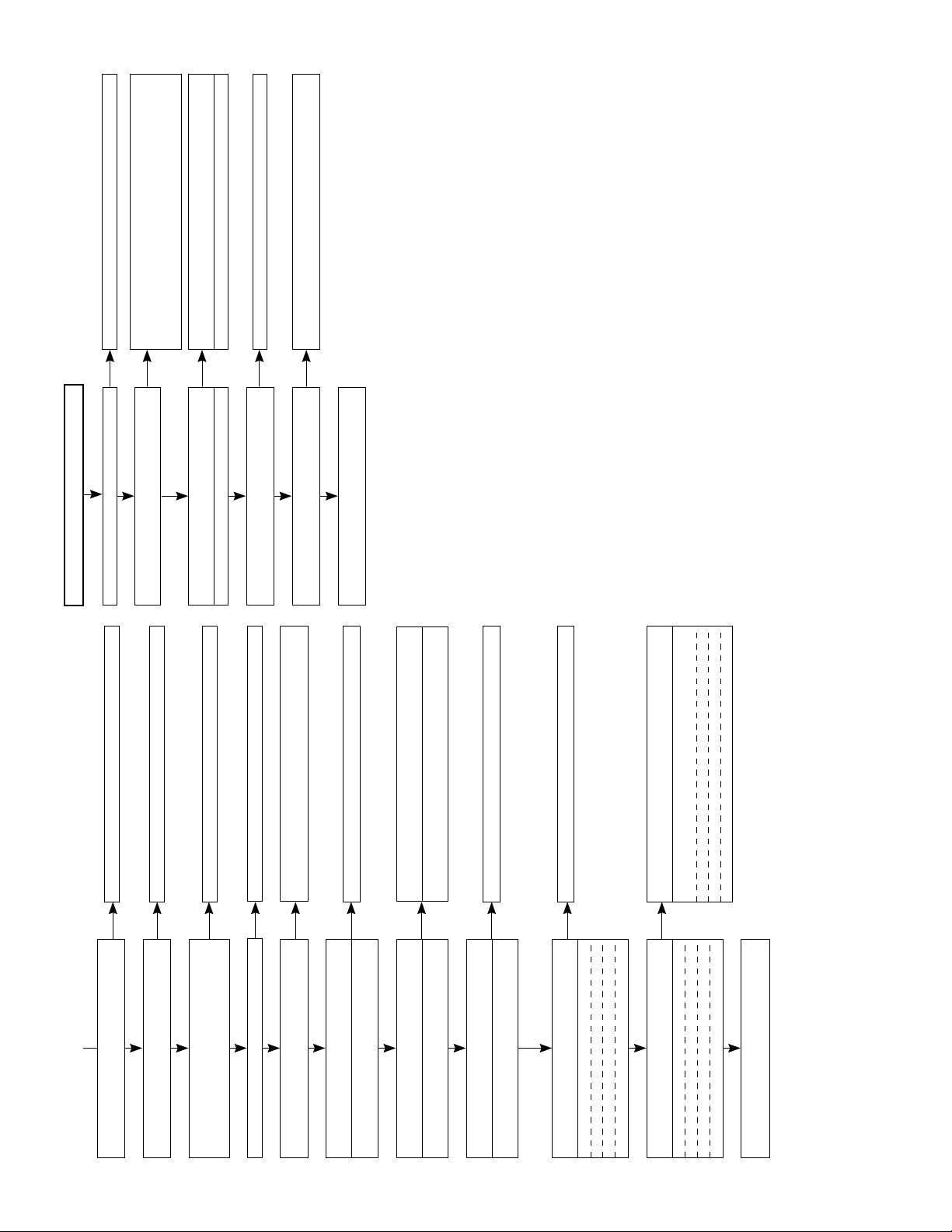
NO
Check lines between pins of CN3001 and IC6501.
CN3001 pin 11 → S2202 pin 11→ IC6501 pin 3 VOUT_L
CN3001 pin 12 → S2202 pin12 → IC6501 pin 5 VOUT_R
Is audio digital signal output to each pin of
IC6501?
IC6501 pin 3 VOUT_L
IC6501 pin 5 VOUT_R
YES
NO
Check lines between pins of IC7506 and IC3009.
IC7506 pin 235 → IC3009 pin 1 154_AMCLK
IC7506 pin 217 → IC3009 pin 2 154_ABCLK
IC7506 pin 222 → IC3009 pin 4 154_ALRCK
IC7506 pin 209 → IC3009 pin 3 154_ADATA
Is audio digital signal output to each pin of
IC3009?
IC3009 pin 1 154_AMCLK
IC3009 pin 2 154_ABCLK
IC3009 pin 4 154_ALRCK
IC3009 pin 3 154_ADATA
YES
NO
Check lines between pins of IC7506 and IC3009.
IC7506 pin 263 → IC3009 pin 8 SPIDAO
IC7506 pin 264 → IC3009 pin 7 SPICLK
IC7506 pin 268 → IC3009 pin 6 DAC1_L
Is system control signal output to each pin of
IC3009?
IC3009 pin 8 SPIDAO
IC3009 pin 7 SPICLK
IC3009 pin 6 DAC1_L
DV-HR300U
21
DV-HR300U
Is audio signal input to IC6101 pins
1, 2, 4, 5, 11, 12, 14 and 15?
FLOW CHART No.12
Sound E-E is not output.
1In external input mode
■ Check lines between rear audio input 1 terminal (J2401) and IC6101 pins 5/14.
■ Check lines between rear audio input 2 terminal (J2701) and IC2461 pins 3/13
as well as lines between IC2461 pins 4/14 and IC6101 pins 4/11.
■ Check lines between front audio input terminal (J2702) and IC6101 pins 2/15.
2In U/V tuner mode
Check these: periphery of U/V tuner (TU1501), line between pin 15 of U/V tuner
and IC1401 pin 15, periphery of IC1401, and lines between IC1401 pins 24/23
and IC6101 pins 1/12.
NO
Is audio signal input to each pin of IC6102?
IC6102 pin 3 INPUT_L
IC6102 pin 5 INPUT_R
NO
Is audio signal output to each pin of IC6101?
IC6101 pin 3 INPUT_L
IC6101 pin 13 INPUT_R
Is 5V applied to IC6101 pin 16, and -5V applied to pin 7?
Check or replace IC6101.
Check PC_5V (1) line and PC_-5V line.
NO
YES
YES
YES
NO
Are voltages of control signal lines T_A MUTE, AUX2 (H)
and AUX1 (H) of pins 6/9/10 controlling IC6101 normal?
Check each control signal line.
Check PC_5V (1) line and PC_-5V line.
YES
NO
Check EE_AMCLK line.
NO
Check lines between pins of IC6101 and IC6102.
IC6101 pin 3 → IC6102 pin 3 INPUT_L
IC6101 pin 13 → IC6102 pin 5 INPUT_R
Is audio signal output to pins of main unit
connector CN3001?
CN3001 pin 8 AUD_L_ADIN
CN3001 pin 7 AUD_R_ADIN
NO
Check lines between pins of IC6102 and CN3001.
IC6102 pin 1 → S2202 pin 8 → CN3001 pin 8
AUD_L_ADIN
IC6102 pin 7 → S2202 pin 7 → CN3001 pin 7
AUD_R_ADIN
Is audio signal input to each pin of IC3002?
IC3002 pin 13 AUD_L_ADIN
IC3002 pin 3 AUD_R_ADIN
NO
YES
YES
Check lines between pins of CN3001 and IC3002.
CN3001 pin 8 → IC3002 pin 13 AUD_L_ADIN
CN3001 pin 7 → IC3002 pin 3 AUD_R_ADIN
1
NO
NO
YES
Refer to Flow chart No.11 "Playback sound is not
output properly".
Check or replace IC3005.
YES
YES
Check IC7506 or peripheral circuits.
1
YES
NO
NO
Is audio digital signal output to each pin of IC7506?
IC7506 pin 235 154_AMCLK
IC7506 pin 217 154_ABCLK
IC7506 pin 222 154_ALRCK
IC7506 pin 209 154_ADAT A
Is audio digital signal output to each pin of IC7506?
IC7506 pin 248 AD_DOUT
IC7506 pin 221 AD_BCK
IC7506 pin 230 AD_LRCK
Is audio digital signal output to each pin of IC3005?
IC3005 pin 9 AD_DOUT
IC3005 pin 12 AD_BCK
IC3005 pin 10 AD_LRCK
Is audio signal output to each pin of IC3005?
IC3005 pin 2 AUD_L_ADIN
IC3005 pin 1 AUD_R_ADIN
ICheck lines between pins of IC3005 and IC7506.
IC3005 pin 9 → IC7506 pin 248 AD_DOUT
IC3005 pin 12 → IC7506 pin 221 AD_BCK
IC3005 pin 10 → IC7506 pin 230 AD_LRCK
YES
Is audio signal output to each pin of IC6102?
IC6102 pin 1 INPUT_L
IC6102 pin 7 INPUT_R
Is 5V applied to IC6102 pin 8, and -5V applied to pin 4?
NO
Is 5V applied to IC3005 pin 6, and 3.3V applied to pin
7?
Is EE_AMCLK signal input to IC3005 pin 11?
Check A_5V line and D_3.3V (1) line.
YES
YES
YES
YES
NO
Check lines between pins of IC3003 and IC3005.
IC3003 pin 7 → IC3005 pin 2 AUD_L_ADIN
IC3003 pin 1 → IC3005 pin 1 AUD_R_ADIN
YES
YES
Is audio signal output to each pin of IC3003?
IC3003 pin 7 AUD_L_ADIN
IC3003 pin 1 AUD_R_ADIN
Is 5V applied to IC3003 pin 8, and -5V applied to pin 4?
Check A_5V line and PC_-5V line.
NO
YES
NO
Check IC3003 peripheral circuits or replace IC3003.
IIs audio signal output to each pin of IC3003?
IC3003 pin 5 AUD_L_ADIN
IC3003 pin 3 AUD_R_ADIN
NO
YES
Check lines between pins of IC3002 and IC3003.
IC3002 pin 14 → IC3003 pin 5 AUD_L_ADIN
IC3002 pin 4 → IC3003 pin 3 AUD_R_ADIN
Is audio signal output to each pin of IC3002?
IC3002 pin 14 AUD_L_ADIN
IC3002 pin 4 AUD_R_ADIN
Is 5V applied to IC3002 pin 16, and -5V applied to pin
7?
Check A_5V line and PC_-5V line.
NO
YES
NO
Check IC3002 peripheral circuits or replace IC3002.
22
FLOW CHART No.13
Audio signal recording is impossible.
Is E-E signal output?
Refer to Flow chart No.12 "E-E sound is not output".
YES
YES
YES
YES
YES
Are drive controls of IC7506 and HDD working properly?
Refer to Flow chart No.2 "Drive is not working
properly (communication failure with IC7506)" or
Flow chart No.3 "HDD is not working properly
(communication failure with IC7506)".
Are the following signals including data output from
IC3008?
Are the following signals including data output from
IC3005 pins to IC3008 pins?
Check lines between pins of
IC3005 and IC3008.
IC3008 pin 7 AIN_ABCK
IC3008 pin 9 AIN_ALRCK
IC3008 pin 12 AIN_ADAT
Are the following signals including data output from
IC7304?
Refer to Flow chart No.4 "Recording is impossible (MPEG
stream check)".
NO
NO
NO
NO
NO
Check IC3008 peripheral circuits or replace IC3008.
IC7304 pin 8 AIN_ABCK
IC7304 pin 7 AIN_ALRCK
IC7304 pin 9 AIN_ADAT
IC3005 pin 12 → IC3008 pin 5 AD_BCK
IC3005 pin 10 → IC3008 pin 11 AD_LRCK
IC3005 pin 9 → IC3008 pin 14 AD_DOUT
Check lines between pins of IC3008 and IC7304.
IC3008 pin 7 → IC7304 pin 8 AIN_ABCK
IC3008 pin 9 → IC7304 pin 7 AIN_ALRCK
IC3008 pin 12 → IC7304 pin 9 AIN_ADAT
Picture/sound input is impossible from DV input terminal.
Is serial communication normal between pins
of IC4005 and IC7506?
IC4005 pin 149 -> IC7506 152 (DV_TXD)
Check IC4005, IC7506 and peripheral circuits, and
lines between pins of IC4005 and IC7506.
YES
Is 27MHz clock signal INVCK4 input from
IC3004 pin 16 to IC4005 pin 50?
Check IC3004 and peripheral circuits, and line
between IC3004 pin 16 and IC4005 pin 50.
Picture
Are video data and video clock input from
IC4005 pins to pins of IC3508 and IC3509?
Check IC4005 and peripheral circuits, and lines bet-
ween IC4005 pins and pins of IC3508 and IC3509.
Is AMCLK input from IC4008 pin 3 to IC4005
pins 103 and 104?
Sound
Check IC4012 and peripheral circuits, and lines
between IC4012 pin 4, IC4008 and IC4005 pins
103 and 104.
IC3508 pins 2-9 DV_656 [7-0]
IC3509 pin 2 DV_DCK
Are video data and video clock input to pins of
IC7506 and IC7304?
IC7506 pins 181-183, 184 and 186-189
VDI_656 [7-0]
IC7506 pin 184 VIDICLK
IC7304 pins 16-23 VDI_656 [7-0]
IC7304 pin 25 VIDICLK
IC3508 pins 11-18 → IC7506 pins 181-183, 184 and
186-189 VDI_656 [7-0]
IC3509 pin 6 → IC3506 → IC7506 pin 184 VIDICLK
IC3508 pins 11-18 -> IC7304 pins 16-23 VDI_656 [7-0]
IC3509 pin 6 → IC3506 → IC7304 pin 25 VIDICLK
IC4005 pins 40-47 → IC3508 pins 2-9
DV_656 [7-0]
IC4005 pin 51 → IC3509 pin 2 DV_DCK
Is clock signal input to each pin of IC4002?
Check IC4005, IC4008 and peripheral circuits, lines
between pins of IC4005 and IC4002 and peripheral
circuits on lines.
IC4002 pin 10 ALRCK
Is audio signal output to each pin of IC4002?
IC4002 pin 15 DV_AUD_L
IC4002 pin 16 DV_AUD_R
IC4005 pin 93 → IC4002 pin 10 ALRCK
IC4002 pin 11 ADMCLK
IC4005 pin 101 → IC4008 → IC4002 pin 11 ADMCLK
IC4002 pin 12 ABCK
IC4005 pin 94 → IC4002 pin 12 ABCK
Is DAC data PCM1 output to IC4005 pin 96?
Check IC4005 and peripheral circuits.
Check line between IC4005 pin 96 and IC4002 pin 9,
IC4002 and peripheral circuits.
FLOW CHART No.14
IC4005 pin 150 <- IC7506 156 (DV_RXD)
Check these: IC3508 and peripheral circuits, lines
between pins of IC3508, IC7506 and IC7304, IC3509,
line between IC3509 output pin and IC7506, lines
between pins of IC7304 and peripheral circuits on lines.
YES
YES
YES
YES
NO
NO
NO
NO
NO
NO
NO
YES
NO
DV-HR300U
23