

Page 1
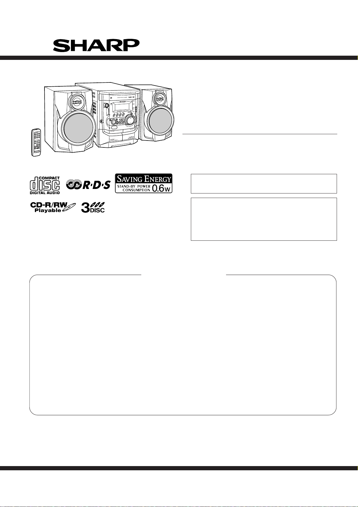
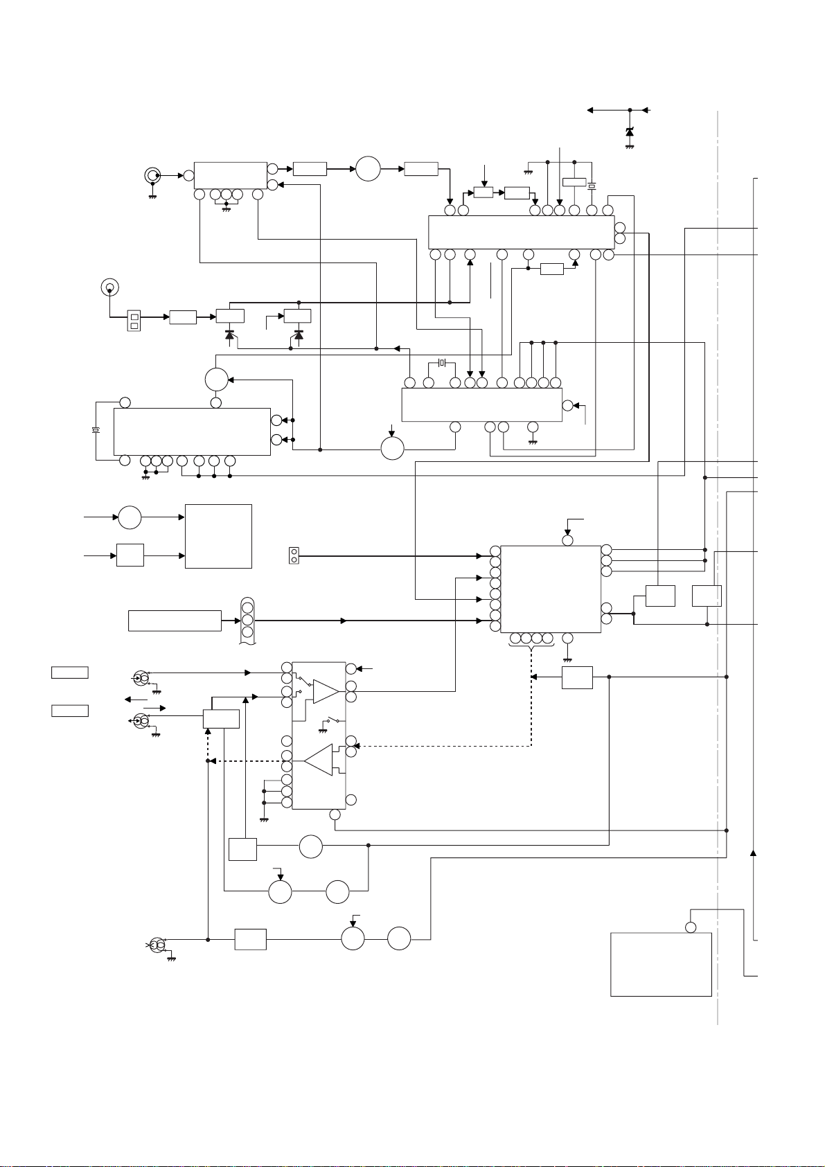
CD-XP200H
SERVICE MANUAL
No. S5236CDXP200H
MINI COMPONENT SYSTEM
MODEL CD-XP200H
CD-XP200H Mini Component System consisting of CD-XP200H
(main unit) and CP-XP200H (speaker system).
• In the interests of user-safety the set should be restored to its
original condition and only parts identical to those specified be
used.
• Note for users in U.K.
Recording and playback of any material may require consent
which SHARP is unable to give. Please refer particularly to the
provisions of Copyright Act 1956, the Dramatic and Musical
Performers Protection Act 1956, the Performers Protection Acts
1963 and 1972 and to any subsequent statutory enactments and
orders.
CONTENTS
Page
SAFETY PRECAUTION FOR SERVICE MANUAL ........................................................................................................... 2
IMPORTANT SERVICE NOTES (FOR U.K. ONLY) .......................................................................................................... 2
SPECIFICATIONS ............................................................................................................................................................. 3
NAMES OF PARTS ........................................................................................................................................................... 4
DISASSEMBLY.................................................................................................................................................................. 6
REMOVING AND REINSTALLING THE MAIN PARTS..................................................................................................... 9
ADJUSTMENT ................................................................................................................................................................. 10
NOTES ON SCHEMATIC DIAGRAM .............................................................................................................................. 14
TYPES OF TRANSISTOR AND LED............................................................................................................................... 14
BLOCK DIAGRAM ........................................................................................................................................................... 15
SCHEMATIC DIAGRAM / WIRING SIDE OF P.W.BOARD............................................................................................. 18
VOLTAGE ........................................................................................................................................................................ 35
WAVEFORMS OF CD CIRCUIT...................................................................................................................................... 36
TROUBLESHOOTING ..................................................................................................................................................... 37
FUNCTION TABLE OF IC................................................................................................................................................ 41
FL DISPLAY..................................................................................................................................................................... 47
WIRING OF PRIMARILY SUPPLY LEADS (FOR U.K. ONLY) ....................................................................................... 48
REPLACEMENT PARTS LIST/EXPLODED VIEW
PACKING METHOD (FOR U.K. ONLY)
SHARP CORPORATION
This document has been published to be used
for after sales service only.
The contents are subject to change without notice.
Page 2
REMOVING AND REINSTALLING THE MAIN PARTS
TAPE 2
TAPE 1
Main Belt
(E1)x1
TAPE 2
Main Belt
(D1)x1
TAPE 1
Main Belt
(D1)x1
Main Belt
(E1)x1
FF/REW
Belt
(D2)x1
FF/REW
Belt
(E2)x1
Motor
Motor
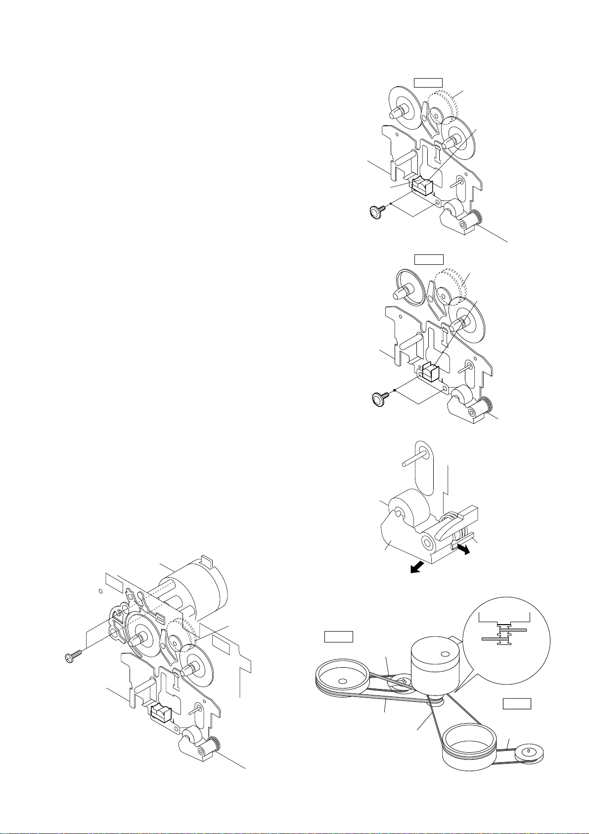
TAPE MECHANISM SECTION
Perform steps 1 to 6 and 8 of the disassembly method to
remove the tape mechanism.
How to remove the record/playback and erase
heads (TAPE 2) (See Fig. 9-1)
1. When you remove the screws (A1) x 2 pcs., the record/
playback head and three-dimensional head of the erasing
head can be removed.
How to remove the playback head (TAPE 1)
(See Fig. 9-2)
1. When you remove the screws (B1) x 2 pcs., the playback
head can be removed.
How to remove the pinch roller (TAPE 1/2)
(See Fig. 9-3)
1. Carefully bend the pinch roller pawl in the direction of the
arrow <A>, and remove the pinch roller (C1) x 1 pc., in the
direction of the arrow <B>.
Note:
When installing the pinch roller, pay attention to the spring
mounting position.
Erase Head
(A1)x2
Ø2x9mm
TAPE 2
Figure 9-1
TAPE 1
CD-XP200H
Clutch Ass'y
Record/Playback
Head
Clutch Ass'y
Playback
Head
How to remove the belt (TAPE 2)
(See Fig. 9-4)
1. Remove the main belt (D1) x 1 pc., from the motor side.
2. Remove the FF/REW belt (D2) x 1 pc.
How to remove the belt (TAPE 1)
(See Fig. 9-4)
1. Remove the main belt (E1) x 1 pc., from the motor side.
2. Remove the FF/REW belt (E2) x 1 pc.
How to remove the motor (See Fig. 9-5)
1. Remove the screws (F1) x 2 pcs., to remove the motor.
Motor
Clutch Ass'y
(F1)x2
Ø2.6x5mm
(B1)x2
Ø2x9mm
Pinch Roller
(C1)x1
Figure 9-2
Pull
Figure 9-3
<B>
<A>
Pinch
Roller
Pawl
Figure 9-4Figure 9-5
– 9 –
Page 3
CD-XP200H
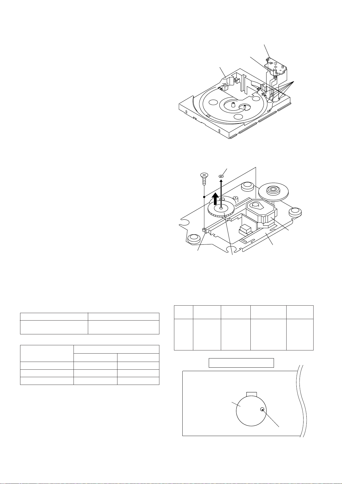
CD MECHANISM SECTION
Perform steps 1, 2, 3, 10, 11, 12 and 13 of the disassembly
method to remove the CD mechanism.
How to remove the loading motor
(See Fig. 10-1)
1. Bend the hooks (A1) x 5 pcs., to remove the loading motor.
How to remove the pickup (See Fig. 10-2)
1. Remove the stop washer (B1) x 1 pc., to remove the gear
(B2) x 1 pc.
2. Remove the screws (B3) x 2 pcs., to remove the shaft
(B4) x 1 pc.
3. Remove the pickup.
Note
After removing the connector for the optical pickup from the
connector wrap the conductive aluminium foil around the front
end of connector so as to protect the optical pickup from
electrostatic damage.
(B3)x2
ø2.6x6mm
Loading
Motor PWB
Loading
Motor
Loading
Tray
(A1)x5
Figure 10-1
Stop Washer
(B1)x1
ADJUSTMENT
MECHANISM SECTION
• Driving Force Check
Torque Meter Specified Value
Play: TW-2111 Tape 1: Over 80 g
• Torque Check
Torque Meter
Play: TW-2111 30 to 80 g.cm 30 to 80 g.cm
Fast forward: TW-2231 — 70 to 180 g.cm
Rewind: TW-2231 — 70 to 180 g.cm
Tape 2: Over 80 g
Specified Value
Tape 1
Tape 2
Pickup
Shaft
(B4)x1
Gear
CD Mechanism
(B2)x1
Figure 10-2
• Tape Speed
Test Tape
Normal MTT-111 Variable 3,000 ± 30 Hz Speaker
speed Resistor in Terminal
Adjusting
Point
motor. (Load
Specified
Value
TAPE MECHANISM
Instrument
Connection
resistance:
6 ohms)
– 10 –
Tape
Motor
Variable Resistor in motor
Figure 10-3
Page 4
CD-XP200H
T
T
EFBL
FDO
TE
Stopped
CH1=500 mV
DC 10:1
CH2=200 mV
DC 10:1
CH3=1 V
DC 10:1
500 ms/div
(500 ms/div)
NORM:20 kS/s
1
2
3
=Record Length=
Smoothing : ON CH1 : 0.000 V
CH2 : 0.000 V
Main : 100K
Zoom : 2k
Mode : SINGLE
Type : EDGE CH1
Delay : 0.0 ns
Hold off : 0.2 µs
CH3 : 0.00 V
CH4 : 0.00 V
BW : FULL
=Trigger==Filter= =Offset=
CH2
v/DIV
200 mV
1999/04/05 20:26:47
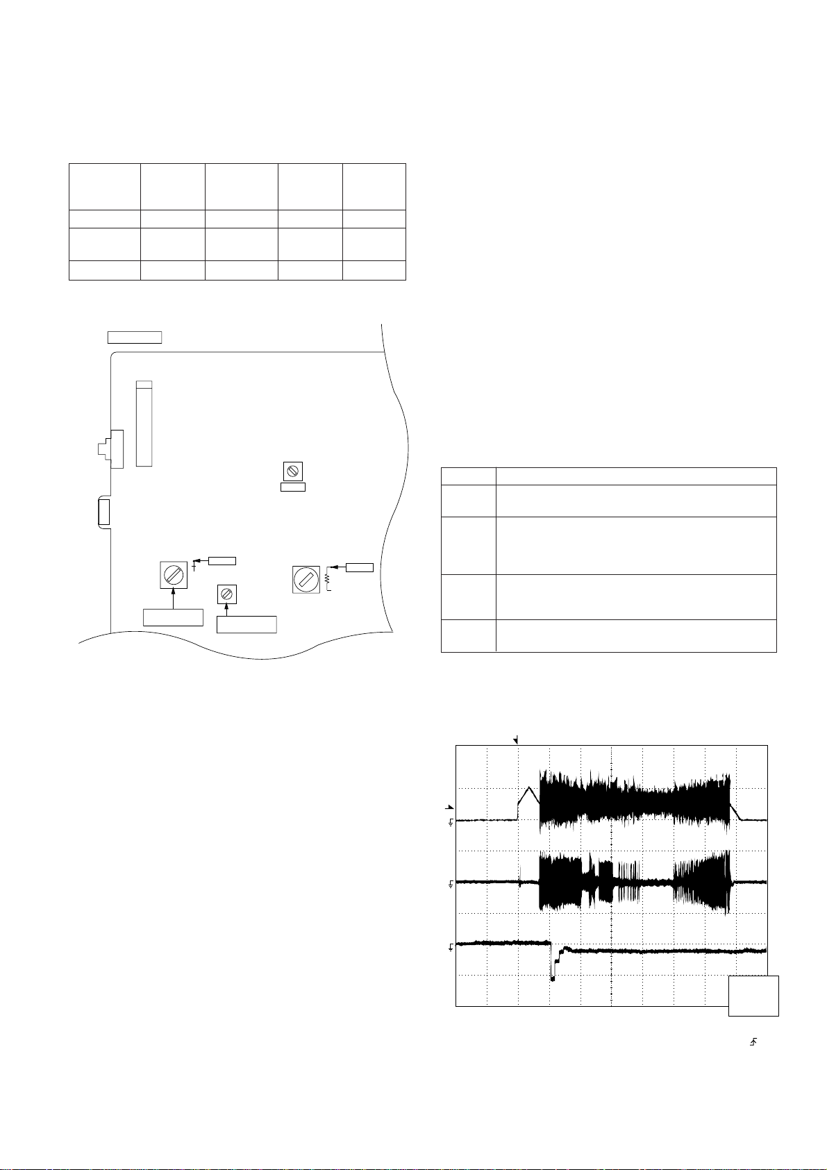
TUNER SECTION
fL: Low-range frequency
fH: High-range frequency
• AM IF/RF
Signal generator: 400 Hz, 30%, AM modulated
Test Stage
AM IF 450 kHz 1,620 kHz T351 *1
AM Band — 522 kHz (fL): T306 *2
Coverage 1.1 ± 0.1 V
AM Tracking 990 kHz 990 kHz (fL): T303 *1
*1. Input: Antenna Output: TP302
*2. Input: Antenna Output: TP301
SO301
TERMINAL
FM ANTENNA
CNP302
ANTENNA
AM/FM LOOP
• FM IF
Notes:
1. Description of the "FM IF Adjustment" is not carried on this
Manual. It is because the IF coil in the FM front end section
has been best adjusted in the factory so that its further
adjustment is not needed at the field. When replacing the
FM front end assembly, no adjustment is needed either.
2. The parts in the FM front end section are prepared in a
complete unit, so you can't obtain each part individually.
Frequency Frequency
Display
MAIN PWB
FE301
T303
AM TRACKING
fL
R336
TP301
T306
AM BAND
COVERAGE fL
Figure 11-1 ADJUSTMENT POINTS
Setting/
Adjusting
Parts
T351
AM IF
L354
R357
Instrument
Connection
TP302
CD SECTION
• Adjustment
Since this CD system incorporates the following automatic
adjustment functions, readjustment is not needed when
replacing the pickup. Therefore, different PWBs and pickups
can be combined freely.
Each time a disc is changed, these adjustments are
performed automatically. Therefore, playback of each disc
can be performed under optimum conditions.
Items adjusted automatically
(1) Offset adjustment (The offset voltage between the head
amplifier output and the VREF reference voltage is
compensated inside the IC.)
* Focus offset adjustment
* Tracking offset adjustment
(2) Tracking balance adjustment (waveform drawing
Fig.11-2 EFBL)
(3) Gain adjustment (The gain is compensated inside the IC
so that the loop gain at the gain crossover frequency will
be 0 dB.)
* Focus gain adjustment
* Tracking gain adjustment
CD ERROR CODE DESCRIPTION
Error
01
When Pickup set inner position, inner switch
cannot detect 'ON' level for 10 secs.
When tray moves to Open/Close, Open/Close switch
10*
cannot detect 'ON' level for 7 secs.
When disc table rotate to target position.
Clamp switch cannot detect 'ON' level for 7 secs.
When disc table set to Disc1 position for 1 st time,
11* "CLAMP SW", "DISC NO SW" and "OPEN/CLOSE"
cannot detect 'ON' level for 14 secs.
31
When it changes to CD function, DSP cannot read
initial data.
* 'CHECKING'
If Error is detected, 'CHECKING' will be display instead of 'ERCD**' display. 'ER-CD**' display will only be display when
error had been detected for the 5 th times.
Explanation
Figure 11-2
– 11 –
Page 5
CD-XP200H
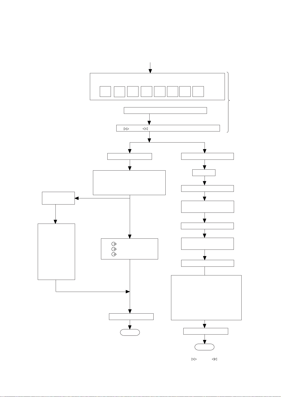
TEST MODE
• Setting the test mode
Any one of test mode can be set by pressing several keys as follows.
<X-BASS> + <CD> + <POWER> TEST: CD operation test.
Function: -CD test mode.
-Enter test mode.
C D T E S T
OPEN/CLOSE operation is using manual.
<< >>, << >> buttons make pick's slide possible.
IL isn't done
<<MEMORY>>
key input.
Adjustment result
automatically will
display as below.
for each 2 sec :
a) "FOFF_XX"
b) "TOFF_XX"
c) "TBAL_XX"
d) "TGAN_XX"
f) "FGAN_XX"
g) "RFLS_XX"
explanation:
a) Focus off set = "FOFF_XX"
b) Tracking off set = "TOFF_XX"
c) Tracking balance = "TBAL_XX"
d) Tracking Gain = "TGAN_XX"
f) Focus Gain = "FGAN_XX"
g) RF level shift = "RFLS_XX"
<<PLAY>> key input.
Do TOC IL. Do normal play.
When these following key is input
into PLAY key, track number can
be appoint directly.
<< 1>> key: Track 4
<<
2>> key: Track 9
3>> key: Track 15
<<
<<STOP>> key input.
STOP
<<MEMORY>> key input.
Laser ON.
<<MEMORY>> key input.
Tracking OFF play at that
specific point.
<<MEMORY>> key input.
Tracking ON play from
that specific point.
<<MEMORY>> key input.
Adjustment result automatically will
display as below for each 2 sec :
a) "FOFF_XX"
b) "TOFF_XX"
c) "TBAL_XX"
d) "TGAN_XX"
f) "FGAN_XX"
g) "RFLS_XX"
<<STOP>> key input.
VOL — Last memory
BAL — CENTER
P.GEQ — FLAT
X-BASS — OFF
To cancel : Power OFF
– 12 –
STOP
Sliding the PICKUP with
>>, << >> button
<<
must only be in STOP mode.
Page 6

CD-XP200H
Standard Specification of Stereo System Error Message Display Contents
Error Contents DISPLAY Notes
TAPE Mechanism Error. 'ER-TA**' 00: Tape Mechanism Error.
01: Initial Error.
CD Pickup Mechanism Error. 'ER-CD**' 01: PU-IN SW Detection NG.
CD Changer Mechanism Error. 'ER-CD**' 10: Changer Error.
(*) 11: Initial Error.
CD DSP Communication Error 'ER-CD**' 31: DSP COMMUNICATION ERROR
Focus Not Match. 'NO DISC'
IL Time Over. 'NOT READ'
TUN PLL Unlock. 'ER-TU**' 00: TUN Error.
01: PLL Unlock.
(*) CHECKING:
If CD changer mechanism error is detected, 'CHECKING' will be display instead of 'ER-CD**' display 'ER-CD**' will only be display
when CD changer mechanism error had been detected for the 5 th times.
Speaker abnormal detection and +B PROTECTION display
In case speaker abnormal detection or +B PROTECTION had occurred, it can be check by pressing 'POWER', 'VIDEO' and 'XBASS' key twice. Display will show "S** B**". S is referring to speaker abnormal detection and B is referring to +B PROTECTION.
** is in hex valve.
+B PROTECTION is condition when irregular process occur on power supply line.
– 13 –
Page 7
CD-XP200H
NOTES ON SCHEMATIC DIAGRAM
• Resistor:
To differentiate the units of resistors, such symbol as K and
M are used: the symbol K means 1000 ohm and the symbol
M means 1000 kohm and the resistor without any symbol is
ohm-type resistor. Besides, the one with “Fusible” is a fuse
type.
• Capacitor:
To indicate the unit of capacitor, a symbol P is used: this
symbol P means pico-farad and the unit of the capacitor
without such a symbol is microfarad. As to electrolytic
capacitor, the expression “capacitance/withstand voltage”
is used.
(CH), (TH), (RH), (UJ): Temperature compensation
(ML): Mylar type
(P.P.): Polypropylene type
• Schematic diagram and Wiring Side of P.W.Board for this
model are subject to change for improvement without prior
notice.
• The indicated voltage in each section is the one measured
by Digital Multimeter between such a section and the chassis with no signal given.
1. In the tuner section,
indicates AM
indicates FM stereo
2. In the main section, a tape is being played back.
3. In the deck section, a tape is being played back.
4. In the power section, a tape is being played back.
5. In the CD section, the CD is stopped.
• Parts marked with “ 1 ” ( ) are important for
maintaining the safety of the set. Be sure to replace these
parts with specified ones for maintaining the safety and
performance of the set.
REF. NO
SW1 OPEN/CLOSE ON—OFF
SW2 CLAMP ON—OFF
SW3 DISC NUMBER ON—OFF
SW4 PICKUP IN ON—OFF
SW701 ON/STAND-BY ON—OFF
SW702 FAST REWIND/PRESET DOWN ON—OFF
SW703 FAST FORWARD/PRESET UP ON—OFF
SW704 STOP ON—OFF
SW705 PLAY/REPEAT ON—OFF
SW711
SW712 TUNER (BAND) ON—OFF
SW713 TAPE ON—OFF
SW714 VIDEO/AUX ON—OFF
SW715 TIMER/SLEEP ON—OFF
CD
DESCRIPTION
POSITION
ON—OFF
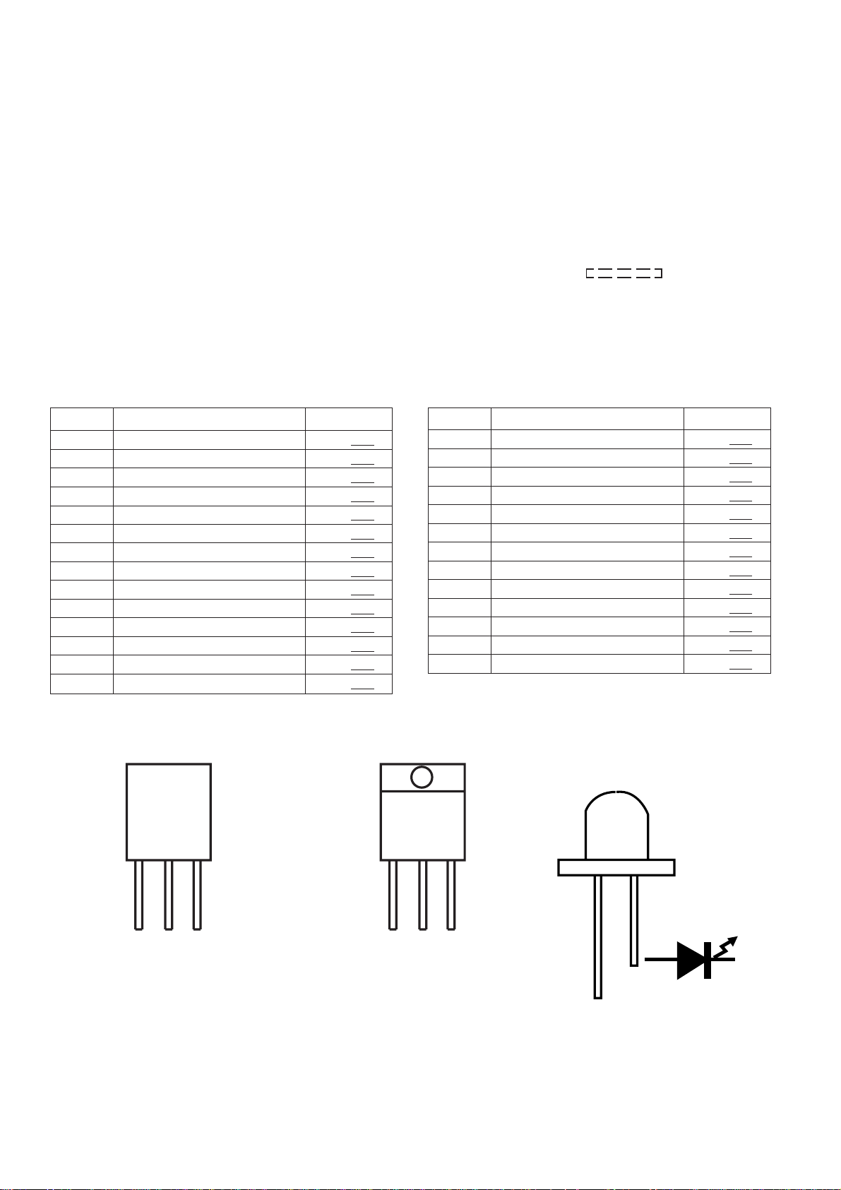
TYPES OF TRANSISTOR AND LED
FRONT
VIEW
REF. NO DESCRIPTION POSITION
SW716 TUNING/TIME UP ON—OFF
SW717 REC PAUSE ON—OFF
SW718 MEMORY/SET ON—OFF
SW719 TUNING/TIME DOWN ON—OFF
SW720 CLOCK ON—OFF
SW721 VOLUME UP ON—OFF
SW722 VOLUME DOWN ON—OFF
SW723 DISC SKIP ON—OFF
SW724 OPEN/CLOSE ON—OFF
SW725 EQUALIZER/X-BASS/DEMO ON—OFF
SW727 DISPLAY MODE ON—OFF
SW728 ASPM ON—OFF
SW729 PTY. TI SEARCH ON—OFF
FRONT
VIEW
FRONT
VIEW
E C B
(S) (G) (D)
(1) (2) (3)
KRC102 M
KRC104 M
KTA1266 GR
KTA1273 Y
KTA1274 Y
KTC3199 GR
KTC3203 Y
2SC380 O
2SC1845 F
B C E
SLR342VCJKTC2026
– 14 –
Page 8
TO MAIN SECTION
TO DISPLAY SECTION
SW1
OPEN/
CLOSE
SW2
CLAMP
SW3
DISC
NUMBER
316452
T/T UP DOWN
M
+–
CD-XP200H
M3
LOADING
MOTOR
BI4
CNP7
XL1
33.8688 MHz
R-CH
12
+3.3V
316452
DISC NO
O/C
CLAMP SW
CD RES
CL
DI
DO
CE
DRF
IC1
RVDD
FIN1
WRQ
FIN2
54
327168910
Q3
71
75
69
CONT2
CONT3
CONT4
LDS
TIN2
TIN1
80
79
987
10
LDD
CONT5
SLDO
SPDO
FDO
TDO
57
56
55
51
50
44
43
40
37
28
19
26
23
22
21
20
CNP8
+5V
316452
17 25
12
40
VCC4
18
VCC1
FOCUS/TRACKING/
VCC2
24
23
VCC3
AGND
354
61
CE
62
CLK
63
DI
64
DO
65
WRQ
66
RES
67
DRF
L-CH
+5V (+B8)
687
42 68 25 70
VDD5
LCHO
+6.5V (+B4)
DGND (DRIVER)
+5V (+B7)
DGND
LC78645NE
CD SERVO
XOUT
48
XIN
49
VDD
XVDD
RFVDD
5
ADAVDD
18
38
LVDD
VVDD
46
41
77
47
CNS4
CNP4
41 3938
42
IC2
M63001FP
SPIN/SLED
DRIVER
35
~~
29
22
21
14
8
+3.3V
+5V(+B7)
PICKUP UNIT
Q2
CONSTANT
VOLTAGE
ZD1
3.3V
LASER
DRIVER
+3.3V
Q1
FOCUS COIL
TRACKING COIL
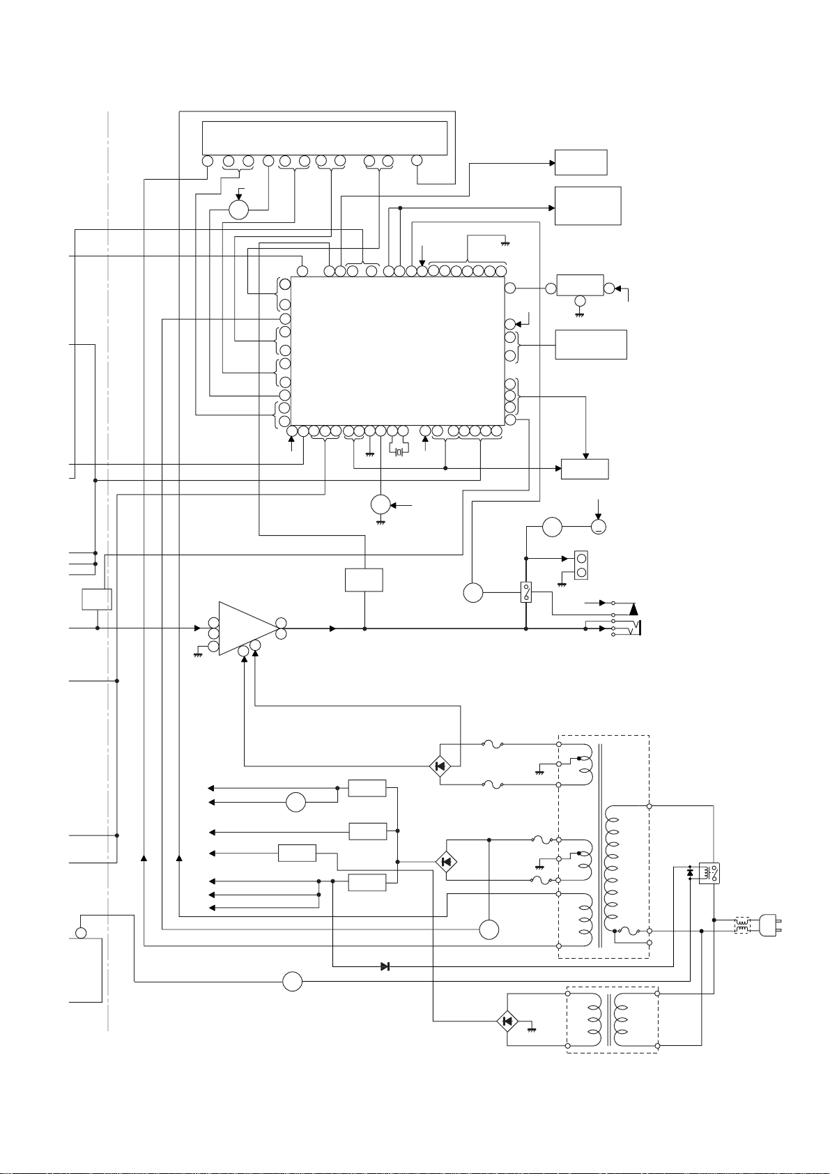
Figure 15 BLOCK DIAGRAM (1/3)
– 15 –
4765
M1
SPINDLE
MOTOR
M2
SLED
MOTOR
M
M
162826 27
15
+
–
–
+
SW4
PICKUP IN
Page 9
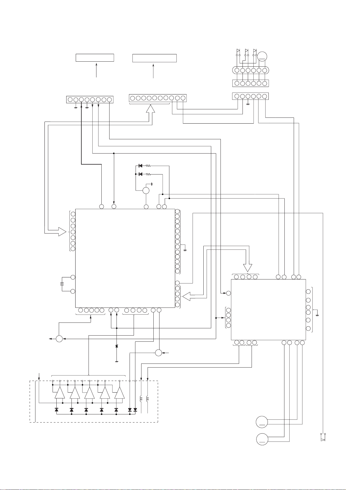
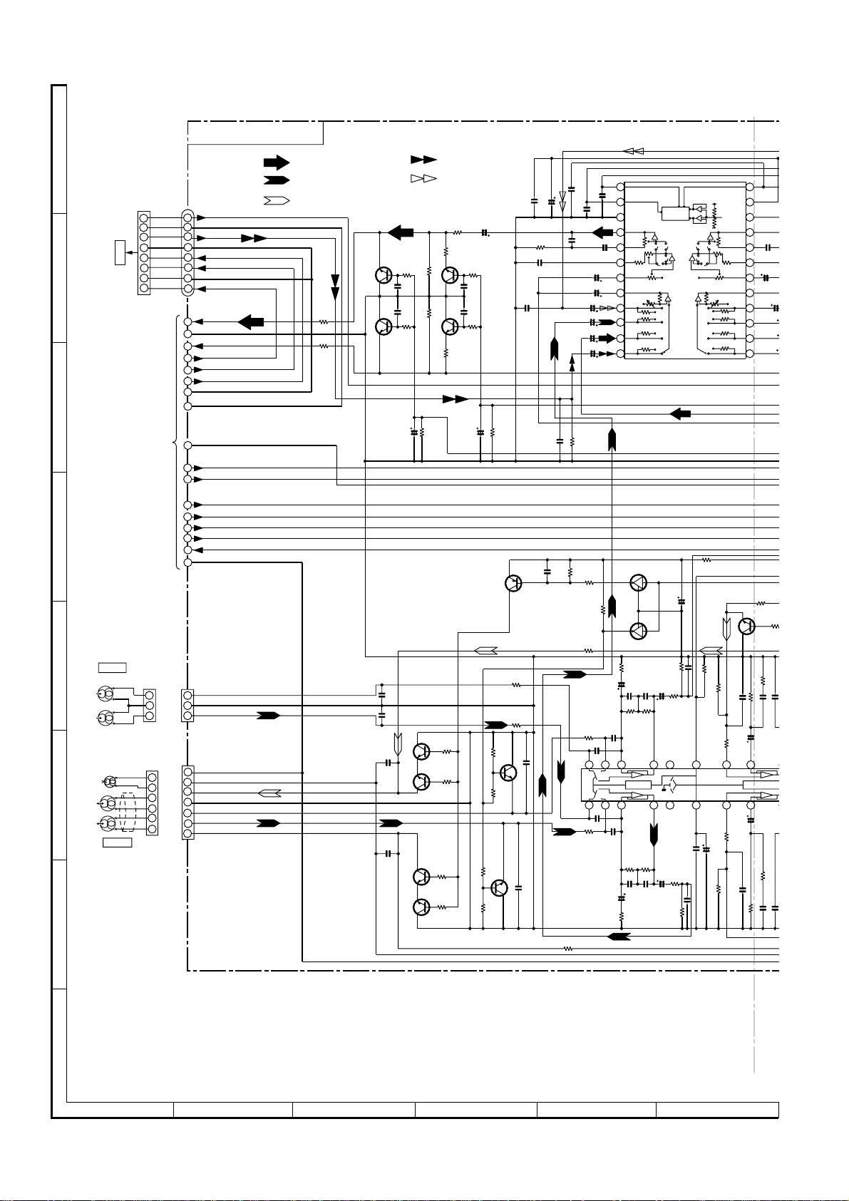
CD-XP200H
SO301
FM ANTENNA
TERMINAL
AM LOOP
ANTENNA
CNP302
ICT21
LC72723
RDS DECORDER
8
X OUT
XT21
4.332 MHz
+B3
+B3
SOLENOID
VSSD
X IN
9
10
74
MOTOR
DRIVER
Q706
Q707
Q708
DRIVER
FROM CD SECTION
FE301
FM FRONT END
8
2
6
7
4
VT
AM
TRACKING
QT21
MPX IN
RST
RDDA
14
13
15
TAPE
MECHANISM
ASS'Y
T303
2
RDCL
RD-ID/
READY
16
BI601
L341
BALUN
TEST
VSSA
CNP7
3
+B6
VDDA
VDDD
1
2
3
CF301
1
5
AM BAND
COVERAGE
T306
3
11
JK690
VIDEO/AUX
L
AUX
R
FM IF
AMP.
Q301
VT
IC302
LC72131
PLL(TUNER)
+B5
FM+B
Q360
SWITCHING
IC303
LA1832S
FM IF DET.
FM MPX./AM IF
CF302
AM OSC OUT
X352
4.5 MHZ
20 22 11
OSC
FM
TUNER
+B6
T351
AM IF
21
AM MIX
21
AM OSC IN
AM RF IN
1615
9
7
L
R
L
TAPE
R
L
R
L
CD
R
FM/AM
9
16
10
15
11
14
12
13
+B6
ZD351
10.7 MHz
CF351
FM
DET
FM+B
MPXIN
12
162324
17
+B5
+B5
23
DI
CE
CLK
3
5.1V
X351
456 kHz
13
VCO
L
MO/ST
R
FM/AM
20
1
2
24
21
4
14
15
R
L
–20dB
ATT
+B6
450 kHz
CF352
4
98517
GND
AM IF
FM/AM
OUT
18
7
L354
LOW PASS
FILTER
STEREO
CLK
DO
DI
CE
5413
6
MO/ST
21
10
IC601
LC75341
AUDIO PROCESSOR
7
81817
+B5
Q601
Q602
Q603
Q604
MUTE
SYSTEM
TAPE 1
P.B. HEAD
TAPE 2
REC./P.B.
HEAD
L-CH
R-CH
L-CH
R-CH
ERASE
HEAD
REC.
P.B.
AC BIAS
SWITCHING
Q101~
Q104
Q105
Q106
Q111
L103
BIAS
OSC
L(T1)
1
24
R(T1)
L(T2)
2
23
R(T2)
6
+B5
Q112
T1/T2
REC
9
16
11
12
NOR/
15
HIGH
SWITCHING
SWITCHING
POP REDUCE
L REC
R REC
SWITCHING
P.B
H/N
T1/T2
19
Q114
Q113
SWITCHING
13
4
21
7
18
10
Q109
+B5
L
PB
R
RECRL
IC101
AN7345K
PLAYBACK AND RECORD
ALC
/PLAYBACK AMP.
+B5
Q110
BIAS
Q107
Q108
MUTING
REC/PLAY
T1/T2
47
IC701
IX0532AW
SYSTEM
MICROCOMPUTER
(2/2)
BIAS
VF1
Figure 16 BLOCK DIAGRAM (2/3)
– 16 –
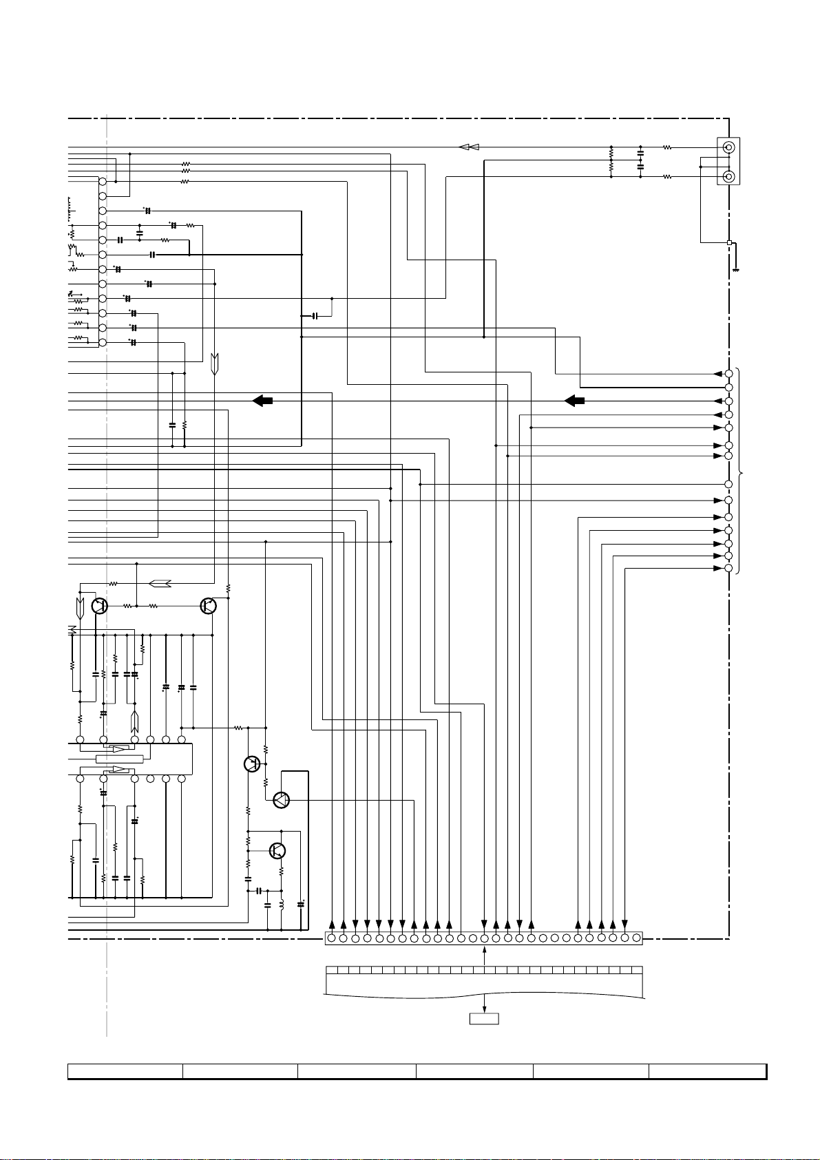
Page 10
51
Q705
CD-XP200H
FL701
FL DISPLAY
45
~
32
27
13
14
12
~
+B9
~
19
~
41
33
+B10
TO CD
SECTION
TAPE
MECHANISM
ASS'Y
Q603
Q604
MUTE
SYSTEM
SP DET.
IC901
STK4029S
POWER AMP.
1
L
15
R
13
9
8
70
~
78
79
VLOAD
80
~
85
86
~
91
92
93
VDD
100
1245678
+B10
L-OUT
7
10
R-OUT
55
~
54 59 623827 5251
40
25 133049 50
46
48
VDD
IC701
IX0532AW
SYSTEM
MICROCOMPUTER
(1/2)
RESET
1 0 16 1 7 20 212223 24
9
XL701
4.194304 MHz
RESET
Q709
Q901~
Q904
1112
VDD
–
+B10
+B10
SP RELAY
ON-OFF
AVDD
CLK
CEDIDO
FAN MOTOR
Q905
RL914
39
+B10
34
33
~
31
37
26
15
41
DRIVER
RX701
REMOTE
1
SENSOR
2
KEY
SW701-SW705
SW711-SW729
TO CD
SECTION
Q906
+B3
HEADPHONES
3
+B10
+B7
M4
M
FAN
MOTOR
SO901
SPEAKER
TERMINAL
JK701
/PLAY
T1/T2
47
UTER
BIAS
VF1
M_13V
+B3
LD+7V
+B4
A_10V
+B5
+B10
+B7
+B8
+B9
UNSW_5.6V
D_5V
A_5V
SW_5V
–VF
VF2
IC853, IC854
VOLTAGE REGULATOR
AC_RLY
-B2
+B2
IC855
VOLTAGE
REGULATOR
IC854
AN78L05
Q841
RELAY
DRIVER
IC851
KIA7812AP
VOLTAGE
REGULATOR
IC851
D802
IC852
F802
T4A L 250V
F801
T4A L 250V
KIA7810AP
VOLTAGE
IC852
IC853
KIA7805AP
D855
REGULATOR
D803,
D804
Q801
D842~
D845
T2A L 250V
F804
T2A L 250V
VOLTAGE
REGULATOR
Figure 17 BLOCK DIAGRAM (3/3)
– 17 –
F803
PT801
MAIN POWER
TRANSFORMER
T.F.
PT841
SUB POWER
TRANSFORMER
RL841
L841
AC LINE
FILTER
AC POWER
SUPPLY CORD
AC 230 V, 50 Hz
Page 11
CD-XP200H
0.7V
0V
0V
0V
0.7V
0V
0V
0V
0V
0V
0V
0.7V
0.7V
0V
0V
0V
9.3V
8.6V
9.3V
0V
3.4V
3.4V
0V
0V
0V
0V
0.7V
24
23
22
21
20
19
18
17
16
15
14
13
12
11
10
9
8
7
6
5
4
3
2
1
24 23 22
1 2 3 4 5
2021
6 7 8
171819
CD(A_GND)
+B_PROTECT
SW_5V
SP_DET
SP_RLY
L-CH
D_5V
R_CH
LD+7V
A_5V
S_MUTE
GND(CD_GND)
GND
(A_GND)
GND(D_GND)
GND(M_GND)
UNSW_5.6V
A_+10V
M_+13.5V
–20dBATT
L
L
R
R
A_GND
T1_R
T1_L
A_GND
M_GND
ERASE
T2_R2
T2_R1
T2_L1
T2_L2
7
6
5
3
2
1
3
1
2
4
CD
TUNER
DECK
AUX
DI
CE
VSS
LOUT
LBASS
LTRE
LIN
L4
L3
L2
L1
CLK
VDD
VREF
ROUT
RBASS
RTRE
RIN
RSEL0
R4
R3
R2
R1
CCB
INTERFACE
+
–
+
–
+
–
+
–
+
–
+
–
+
–
+
–
LSEL0
–
+
–
+
Hich=T1
+
+
–
–
Hich=CHRO
56
112K
56
112K
8
7
1
4
6
5
3
2
D_GND
LD+7V
A-5V
D_5V
CD_GND
L-CH
A_GND
R-CH
8
7
6
5
4
3
2
1
P22 1 - E~G
TO POWER SECTION
TAPE 1
PLAYBACK HEAD
R-CH
L-CH
3
2
1
R-CH
ERASE HEAD
RECORD/
PLAYBACK HEAD
TAPE 2
L-CH
1
4
6
5
2
3
1
1
23
23
CNP7
P27 12 - D
TO CD SERVO PWB
MAIN PWB-A1 (1/3)
1
2
3
7
9
6
8
5
4
11
10
13
16
15
12
14
17
Q603, Q604: SYSTEM MUTE
SWITCHING
SWITCHING
SWITCHING
MUTING
SWITCHING
SWITCHING
SWITCHING
SWITCHING
SWITCHING
SWITCHING
+B
+B
+B
+B
+B
+B
+B
Q101
2SC1845 F
C103
180P
Q103
2SC1845 F
R105
3.3K
R103
2.2K
R107
47K
R109
4.7K
Q105
KTC3199 GR
C105
560P
C104
180P
C101
560P
C102
560P
Q102
2SC1845 F
R104
2.2K
Q104
2SC1845 F
R106
3.3K
R102
1K
R101
1K
R108
47K
R110
4.7K
C106
560P
Q106
KTC3199 GR
Q112
KTA1266 GR
C136
0.022
R146
10K
R147
10K
Q113
KRC104 M
C141
100/16
R149
150
Q114
KRC104 M
R112
15K
C112
100/25
R116
56
R122
10K
R118
100K
R120
3.9K
C116
560P
C114
0.033
C118
47/25
R124
5.6K
C120
0.0022
R150
68K
R126 4.7K
Q108
KTC3199 G
R136
220K
R13
10K
C126
22/50
R128
5.6K
C124 270P
R130 1.5K
C128
0.022
R132
100
IC101
R113
1K
C109
330P
C107
330P
C108
330P
C110
330P
R111
15K
R115
56
C111
100/25
C113
0.033
R117
100K
R119
3.9K
R121
10K
C117
47/25
C115
560P
C119
0.0022
R127
4.7K
C121
0.022
R129
5.6K
C125
22/50
R133
100
C123
270P
C127
0.022
C129 0 0033
CNP102
CNP101
R148
4.7K
C625
0.0022
R609
1.2K
R621
22K
C639
1/50
R620
22K
C640
22/50
R618
330
R619
330
Q603
KTC3199 GR
R617
2.2K
C637
0.001
C638
0.001
R616
2.2K
R614
4.7K
R615
4.7K
Q601
KTC3199 GR
R613
390
R605
10K
C609
1/50
R611
2.2K
C636
0.001
C635
0.001
R610
2.2K
R612
390
Q602
KTC3199 GR
C611
0.0022
C629
0.001
R607
3.9K
C602
0.022
C601
220/16
C653
220P
C652
220P
C651
220P
C607
0.12
C605
0.12
C613
1/50
C615
4.7/50
C617
1/50
C619
1/50
C621
1/50
C623
1/50
IC601
LC75341
AUDIO PROCESSOR
C606
0.12
C61
1/5
C618
1/50
R114
1K
R123
5.6K
Q604
KTC3199 GR
BI601
CNS601
C130 0 0033
C143
3.3/50
R131
1.5K
FM SIGNAL
PLAYBACK SIGNAL
RECORD SIGNAL
CD SIGNAL
VIDEO SIGNAL
A
B
C
D
E
F
G
H
• NOTES ON SCHEMATIC DIAGRAM can be found on page 14.
1
23456
Figure 18 SCHEMATIC DIAGRAM (1/10)
– 18 –
Page 12
CD-XP200H
R127
C143
CLK
VDD
VREF
ROUT
RBASS
RTRE
RIN
RSEL0
R4
R3
R2
R1
OR
BATT
0V
0V
R126 4.7K
28
K
01
7 8
R129
5.6K
3.3/50
C123
4.7K
24
23
+B
22
21
20
C606
0.12
19
18
C614
1/50
17
C618
1/50
16
15
14
13
R136
220K
R138
10K
0.7V
Q108
KTC3199 GR
MUTING
100
R132
C128
C124 270P
0.022
R130 1.5K
C126
22/50
1718 13141516
–
+
56K
Hich=CHROME
56K
+
–
C125
22/50
100
R133
270P
C127
0.022
1.5K
R131
R601 1K
R602 1K
R603 1K
C603
22/50
C610
1/50
C608
0.12
C612
0.0022
C616
4.7/50
C620
1/50
C622
1/50
C624
1/50
C626
R139
10K
KTC3199 GR
10K
R134
C130 0.0033
C132
47/25
C133 22/50
Nor/CrO2
ALC
ALC
10 11 12
9
C131
47/25
R135
10K
C129 0.0033
R604
10K
R606
3.9K
R608
1.2K
0.0022
REC_R
0.7V
Q107
MUTING
C134 220/10
C135 0.022
VCC
RIPPLE
GND
0V
IC101
AN7345K
R137
220K
R158
220
Q109
SWITCHING
PLAYBACK AMP.
C137
PLAYBACK AND RECORD/
REC_L
11.7V
11.6V
0V
KTA1266 GR
R141
4.7K
11.6V
R142
KRC104 M
82(1/2W)
47K
R143
0V
R144
22K
C138
0.0082(PP)
0.047(ML)
C139
0.039(ML)
C630
0.001
R140
47K
1
0V
23
0V
Q110
BIAS
0V
Q111
0V
KTC3203 Y
R145
4.7
L103
330µH
T-T1 T2
REC/PLAY
T_BIAS
BIAS OSC
C140
47/25
–20dB
1
SP_DET
SP_RLY
2
345
+B
+B
SW_5V
UNSW5.6V
+B
+B
+B
+B
A_+10V
A+10V
6
T_BIAS
M_+13.5V
8
7
D_GND
LVL_DET
+B-PROTECT
D_GND
S_MUTE
T_T1/T2
REC/PLAY
11 12 13 14 15 16 17 18 19
10
9
C691
R691
6.8K
R690
6.8K
DI
CE
DO
CLK
KOK_LATCH
MIC IN
SPANCERDS_READY
RDS_RDCL
RDS_RDDA
24
RDS_RST
25 26
DO
CLK
DI
20 21 22 23
390P
C690
390P
TUN_SM
27
CNP601
R693
33K
R692
33K
TUN_R
A GND
TUN_L
D_GND
A_+10V
RDS_READY
RDS_RDCL
RDS_RDDA
RDS_RST
TUN_SM
CLK
DO
CE
DI
L-CH
AUX IN
R-CH
JK690
VIDEO/AUX
CHASSIS
18
2
19
20
21
22
23
15
8
28
27
26
25
24
P21 8, 9 - G
TO TUNER SECTION
1
FFC701
CNP701
P24 1 - F
TO DISPLAY PWB
7
8 9 10 11 12
27
Figure 19 SCHEMATIC DIAGRAM (2/10)
– 19 –
Page 13

CD-XP200H
L
CH OUT
A
CHASSIS
GND
B
C
AM LOOP
ANTENNA
D
E
F
CHASSIS
GND
FM
75 OHMS
SO301
FM
ANTENNA
TERMINAL
1
1
2
2
CNP302
D301
DS1SS133
D302
DS1SS133
L341
BALUN
D303
DS1SS133
D304
DS1SS133
ANT
C302
0.001
GND
GND
C323
0.022
COVERAGE fL
C345 0.022
C346 0.022
C321 100/16
L342
2.2 µH
R369 15
VCC
FM FRONT END
AM TRACKING
AM ANTENNA
AM BAND
T306
AM OSC.
FM SIGNAL
AM SIGNAL
R345 4.7K
VT
F OUT
FE301
T303
C335
560P
C334
22P
(UJ)
C347 0.022
1
R344 470
C341
0.022
GND
2
CF301
R347
R346
330
12345678
IF OUT
R348
680
3
6.8K
C330
15P
(UJ)
VD301
SVC348S
R323
68K
C331
0.047
R336
10K
TP301
R349 33
FM IF AMP.
Q301
2SC380 O
R399
33
C348
0.01
C332
0.022
1
2
+B
C342
0.022
3
CF302
R382
C381
12P(CH)
X352
4.5 MHz
C382
15P(CH)
R365
10K
R358
3.9K
C361 0.022
C362 3.3/50
AM OSC IN
AM OSC OUT
R351 5.6K
C351 0.022
+B
C397
0.022
R381
150
10K
X IN
123456789
C383
56P
AM MIX OUT
FM IF IN
123 456 78 9
T351
AM IF
C350 0.022
C352 10/50
C394
C392
47/25
0.001
C380
10/50
R380
C389
1.5K
1/50
VSS
AOUT
X OUT
DI
CE
R374 1K
R373 1K
C364 2.2/50
C363 0.022
FM AFC
AM RF IN
REG
R352
1K
123
C387
2.2K
R379
PD
AIN
VDD
DO
CLK
FM/AM
LC72131
PLL(TUNER)
R378 1K
R372 1K
C366 0.001
C365 0.022
VSM
FM/AM OUT
AM LOW CUT
AM IF IN
CF352
C393
0.022
0.001
100 µH
C385
0.01
FM IN
AM IN
IF
FM/AM
CONT
10 11
IC302
L354
LOW PASS FILTER
R350
2.7K
X351
C367
456 kHz
1/50
GND
SD
STEREO
FM DET
C353
0.022
C354 0.022
CF351
R393
1K
R377
L351
47K
C386
1213141516171819202122
330P
SD
IF IN
MO/ST
ST IND
R376
1K
R386
22K
R353
270
TP302
MPX VCO
C399
0.022
+B
R395
47K
R360
4.7K
VCC
MPX IN
10 11
C398
470K
R357
1K
R356
C368
IF OUT
C357
2.2/50
C356
0.001
100/10
1/50
PHASE
C374 0.015
C369
27P(UJ)
1415161718192021222324
-
R-CH OUT
C358
1/50
22P
C355
3.9K
R388
5.6K
R387
G
H
• NOTES ON SCHEMATIC DIAGRAM can be found on page 14.
1
23456
Figure 20 SCHEMATIC DIAGRAM (3/10)
– 20 –
Page 14

CD-XP200H
CF351
MAIN PWB-A1 (2/3)
ILTER
TP302
470K
R357
1K
R356
C374 0.015
1/50
C399
+B
0.022
R395
MPX IN
MPX VCO
VCC
C398
100/10
47K
R360
4.7K
C368
IF OUT
PHASE
C357
2.2/50
C356
0.001
C369
R-CH OUT
C358
1/50
C355
3.9K
R388
5.6K
R387
27P(UJ)
22P
351
6 kHz
FM DET
8910 11 12
R353
270
7
R386
22K
C373
0.015
C371
1/50
C372
1/50
1314151617
MO/ST
L-CH OUT
(FM/AM)
PHASE
R355
3.3K
R359
IC303
1/50
C370
L352
100 µH
100/10
SWITCHING
KTA1266 GR
R385
1.8K
+B
8.2K
R363
LA1832S
FM IF DET./
FM MPX./AM IF
ZD351
DZ5.1BSB
C396
C395 0.022
R392
270
R391
Q360
270
+B
R383
5.6K
5.6K
C391
47/25
R384
5.6K
8.2K
R364
C388
0.001
C384
0.001
R370
1K
RT31
10K
1K
RT27
CT21
RT28
1K
RT30
47/25
1K
RT32
6.8K
RT21
10K
RT29
CT22
LT21
1K
CT23
22P(CH)
XT21 4.332 MHz
ICT21
LC72723
XIN
9
VSSD
10
0.022
VDDD
11
MODE
12
RST
13
RDDA
14
RDCL
15
RDS-ID/
READY
16
RDS
2.2 µH
DECORDER
CT24
47/25
ZDT21
DZ5.1BSB
XOUT
TEST
CIN
FLOUT
VSSA
VDDA
MPXIN
VREF
RT24
56K
10K
CT28
0.022
CT29
0.022
RT26
56K
QT21
KTC3199 GR
CT30 0.022
CT31
47/25
CT32
47/25
RT23
390
CT25
22P
(CH)
RT25
8
7
CT26
6
560P
5
CT27
4
0.022
3
2
1
LT22
2.2 µH
RT22
390
+B
+B
TUN_R
TUN_L
TUN_SM
RDS_RST
RDS_RDDA
RDS_RDCL
A_GND
D_GND
A+10V
DO
CLK
DI
CE
21 2827262524191816148202322
TO MAIN SECTION
P19 12 - C, D
7
8 9 10 11 12
RDS_READY
Figure 21 SCHEMATIC DIAGRAM (4/10)
– 21 –
Page 15

CD-XP200H
47
100/35
A
B
C
D
E
F
G
C907
820P
R903
1K
C903
0.001
C901
L-CH
1
(A_GND)
2
3
4
5
M_+13.5V
6
7
8
+B_PROTECT
9
P18 2 - B~D
10
TO MAIN SECTION
11
12
(CD_GND)
13
UNSW_5.6V
14
15
16
17
C905
3.3P
(CH)
R907
R911
R901
0.22/50
GND
R-CH
SP_RLY
SP_DET
LD+7V
A_+10V
D_5V
A_5V
SW_5V
GND
GND (D_GND)
CD(A_GND)
GND (M_GND)
56K
820
C909
4.7/50
56K
L-CH
CH1
+
–
R925
C913
100/63
R921
100(1/4W)
Fusible
R909
1K
22K
5 4 3 2 1
0.22
C932
0.1 (1W)
L
FAN MOTOR 5V
+B
+B
CH1
OUT
R917
R919
0.22(2W)
R913
R923
1K
C911
0.022
R915
1.5K
Q901
KTC3199 GR
+B
+B
VOLTAGE REGULATOR
+B
22K
R859
+B
+VCC
0.22(2W)
+B
+B
IC855
KTC2026
C863
22/50
D857
DS1SS133
C861
C915
10/63
D905
DS1SS133
ZD852
DZ8.2BSB
IC854
AN78L05
+B
0.047(ML)
–VCC
CH2
9 8 7 6
R918
0.22(2W)
C916
10/63
+B
+B
220
R860
C865
D852
DS1SS133
D851
DS1SS133
R852
10K
3 1
2
C860
47/25
D856
DS1SS133
R-CH
C914
100/63
DS1SS133
1K
R924
22K
R854
R
CH2
R922
100(1/4W)
D906
Q902
KTC3199 GR
56K
R902
KIA7812AP
13V
C852
22/50
OUT
R914
0.1 (1W)
C912
0.022
R916
1.5K
C902
0.22/50
C851
10/50
R920
0.22(2W)
0.047(ML)
+B +B
22K
R853
D860
1N4004S
C853
+B
47/25
+B
C857
47/25
+B
C862
10/50
IC851~IC854
VOLTAGE REGULATOR
+
–
1413121110
C908
820P
820
R912
56K
Fusible
R908
C910
4.7/50
D907
DS1SS133
Q904
KTC3199 GR
C904
0.001
R926
22K
R927
22K
IC851
3 1
2
D858
DS1SS133
D859
DS1SS133
IC852
KIA7810AP
3
1
2
C854
C855
0.1(ML)
0.1(ML)
D855
DS1SS133
3 1
2
C858
C859
0.022
0.1(ML)
R858
220
STK4029S
POWER AMP.
15
C906
3.3P(CH)
1K
1K
R910
R904
Q903
KTC3199 GR
C925
C948
2200/56
C949
2200/56
+B
C864
0.1(ML)
+B
IC853
KIA7805AP
IC901
47/50
18V
R935
56K
R936
56K
R937
+B
+B
56K
+B
R942
R938
680
680
R943
R939
680
680
R945
RL914
R946
47K
1.5K
L
R
L
R
C926
C927
0.22
0.22
C928
C929
0.22
0.22
R940
R941
4.7
4.7
D911
DS1SS133
Q905
KTC3199 GR
SP RELAY
ON-OFF
+B
BI801
1
2
3
+B2
+B
4
5
6
7
+B
C856
3300/35
P25 12 - E
CNP801
CNS801
VCC
1
1
GND
2
2
–VCC
3
3
4
4
5
5
676
7
CNP802
1
2
3
CNS705
4
5
FROM DISPLAY PWB
VF2
–VF
P_IN
VF1
AC_RLY
R801
220K
R803
R804
+
C801
12K
47
R805
H
• NOTES ON SCHEMATIC DIAGRAM can be found on page 14.
1
23456
Figure 22 SCHEMATIC DIAGRAM (5/10)
– 22 –
Page 16

CD-XP200H
+B
+B
R938
680
R943
680
D911
DS1SS133
Q905
KTC3199 GR
SP RELAY
ON-OFF
R942
680
R939
680
RL914
R946
47K
R945
1.5K
R944
1.5K
FM SIGNAL
+B
+B
R947
15K
+B
L_OUT
R_OUT
D912
DS1SS133
C931
10/50
C930
47/50
R950
R949
68K
1K
M_+13.5V
SP_RLY
R-CH
GND
L-CH
HLD803
Q906
KTC3203 Y
FAN MOTOR
1
5
CNP971
2
1
DRIVER
FW803
CNS971
+
2
–
1
FAN MOTOR
M
M4
CNP705
+B
1
2
L702
3
2.2 µH
4
5
HEADPHONES
C718
0.001
C719
0.001
JK701
HEADPHONES
PWB-B2
L921
0.29 µH
C939
C935
0.022
+B
0.022
C937
0.022
R953
6.8
C941
0.022
R955
6.8
L920
0.29 µH
C934
C938
0.022
0.022
C936
C940
0.022
0.022
R954
C943
0.001
6.8
R952
6.8
MAIN PWB-A1 (3/3)
C942
0.001
+
SP_L-CH
+
SP_R-CH
–
SP_L-CH_GND
–
SP_R-CH_GND
SO901
SPEAKER
TERMINAL
6 OHMS MIN
When Servicing, pay attention as the
area enclosed by this line ( ) is
directly connected with AC main voltage.
CNP801
CNS801
FROM DISPLAY PWB
1
2
3
4
5
676
CNS705
1
2
3
4
5
7
1
2
3
4
5
VCC
GND
–VCC
CNP802
VF2
–VF
P_IN
VF1
AC_RLY
R801
220K
12K
R803
R804
C809
D803
1N4004S
D804
1N4004S
C803
47K
–28V
Q801
KTA1274 Y
VOLTAGE
REGULATOR
R842
1K
47/50
R808
0.1(ML)
C808
0.1(ML)
ZD803
DZ300BSB
2.2K
(1/2W)
R843
47K
RELAY
DRIVER
D805
1N4004S
C804
220/63
R841
220K
C841
Q841
KTC3199 GR
1000/6.3
+B
D802
+B
D3SBA60F
C807 0.1(ML)
C806 0.1(ML)
ZD802
R802
DZ6.2BSA
47K
C801
100/35
C802
R806
47/50
–28V
–33V
R807
R805
47
ZD801
DZ6.2BSA
10
47
T4A L 250V
T4A L 250V
C805
22/100
D806
1N4004S
D842~D845: 1N4004S
D845
C842
470/35
F802
F801
D844
F803
T2A L 250V
F804
T2A L 250V
D842
D843
C843
0.047(ML)
TRANSFORMER
1
4
HLD804B
PT801
MAIN POWER
FW804
K801
K802
AC POWER
SUPPLY CORD
RL841
C844
L841
AC LINE
FILTER
0.0047
T.F.
HLD804A
1
4
D846
DS1SS133
PT841
SUB POWER
TRANSFORMER
AC 230 V, 50 Hz
TRANSFORMER PWB-A3POWER PWB-A2
7
8 9 10 11 12
Figure 23 SCHEMATIC DIAGRAM (6/10)
– 23 –
Page 17

CD-XP200H
R
R
R
R
R
R
R
R
R
R
R
R
R
R
R
R
4
R
R
R722 1K
A
B
C
D
E
P19 10 - H
TO MAIN PWB
F
TAPE MECHANISM
PWB-F
TAPE
G
MOTOR
-
M
+
SOLENOID
SOLENOID
PLAY
F. PLAY
CASSETTE
H
CNP601
FFC701
PH
27
1
TUN SM
RDS-RST
RDS-RDDA
RDS-RDCL
RDS-READY
SPAN
MIC IN
KARAOKE LATCH
+B_PROTECT
LVL_DET
D_GND
S_MUTE
T_T1/T2
REC/PLAY
T_BIAS
M_+13V
A+10V
SW_5V
UNSW5.6
SP_DET
SP_RLY
–20dB
FFC702
1
1
2
3
4
5
6
7
8
8
DISPLAY PWB-B1
CNP701
27
26
25
24
23
22
21
20
19
CE
18
DO
17
CLK
16
DI
15
14
13
12
11
10
9
8
7
6
5
4
3
2
1
CNP702
T2_PLAY SW
1
GND
2
T2 RUN
3
+MTR
4
SOL2
5
SOL1
6
F_REC
7
T1 RUN
8
C706
47/25
FL701
R794
1.5
C707
1/50
R792
100K
Q705
KTC3199 GR
R752
33
R738
47K
DS1SS133
DS1SS133
R772
D710
DS1SS133
10K
R770
10K
DS1SS133
R740
4.7K
+B
+B
P21
P20
P19
P18
P17
P16
P15
NPF F
45 44 43 42 41 40 39 31 38 37 36 35 34 33 32
R793
1K
D702
D701
R789
R788
10K
10K
D709
C712
47/25
P14
MOTOR
DRIVER
KTA1273 Y
KTA1273 Y
Q707, Q708: SOLENOID DRIVER
P13
Q708
P12
Q707
P11
P10
30 29 28 27
R745 1K
R744 1K
R743 1K
R742 1K
FPA/FPB
Q706
KTA1273 Y
FL DISPLAY
P09
P08
P07
NXNXNXNXNXNXNX
81 82 83 84 85 86 87 88 89 90 91 92 93 94 95 96 97 98 99
80
S11
79
S13
78
77
S14
76
S15
S16
75
74
S17
73
S18
S19
72
S20
71
S21
70
DIST
69
68
67
66
65
64
63
62
RDS READY/ESS DO
61
RDS RDCL/ESS DI
60
RDS RDDA/ESS STB
59
RDS RST/ESS ACK
58
57
56
R746
55
MIC SW
1K
54
O/C_SW
R734
53
1K
52
51
R735
50 49 48 47
1K
R732
1K
+B
R780
10K
M_+13V
+B
R777
10K
+B
R778
10K
+B
R779
10K
P06
P05
P04
19 18 17 16 15 14 13 1226 25 24 23 22 21 20 11 10
S6S7S8
S9
S10
S12
80
79
VLOAD
IX0532AW
MICROCOMPUTER
52
T1 RUN
T2 RUN
51
T_SOL_A
T_MOTOR
TIMER LED
VDD
AC_RLY
SP_
RLY
45 444643 42 41 40 39 3138 37 36 35 34 33 32
10K
R731
R730 1K
10K
R762
+B
R727 680
R728 2.2K
R729 560
R726 680
P03
P02
P01
G09
S1S2S3S4S5
G9G8G7G6G5G4G3G2G1
–20dBATT
IC701
SYSTEM
T2_PLAY SW/
FPA/FPB SW
PROTECT
LVL_DET
T_SOL_B
REMOCON
VSS
SMUTE
R724 1K
R725 1K
R733 1K
R765
4.7K
LED701
SLR342VCJ
G05
G06
G07
G08
9876543
1
VDD
2
28
29
30
DISC_NO SW/
P_IN
AVREF
SP DET
CD CLAMP SW
R721 1K
R736 1K
4.7K
R756
R761
10K
R768
R767
R766
G03
G04
T-BIAS
T_T1/T2
REC/PLAY
CD RESOUT
RESET
VPP/IC
CD CLK
CD DI
CD DO
CD CE
DSA DATA
AVDD
KEY 0
R720 1K
10K
10K
10K
G01
G02
100
WRQ
SPAN
X2
X1
13
DRF
15
VDD
CE
CLK
DI
DO
AVSS
KEY 2
KEY 1
R718 1K
R719 1K
1
2
3
4
5
6
7
8
9
10
11
12
14
R
16
17
18
19
20
21
22
23
24
25
26
27
28
29
30
• NOTES ON SCHEMATIC DIAGRAM can be found on page 14.
1
23456
Figure 24 SCHEMATIC DIAGRAM (7/10)
– 24 –
Page 18

G03
R724
1K
G04
G05
G06
G07
G08
G09
13 12 11 10
987654321
92 93 94 95 96 97 98 99
G9G8G7G6G5G4G3G2G1
1
VDD
–20dBATT
2
T_T1/T2
REC/PLAY
CD RESOUT
01
2AW
EM
MPUTER
PLAY SW/
/FPB SW
PROTECT
LVL_DET
REMOCON
SP DET
39 3138 37 36 35 34 33 32
R733 1K
28
29
30
DISC_NO SW/
DSA DATA
CD CLAMP SW
AVDD
P_IN
AVREF
R721 1K
R736 1K
CD CLK
R720 1K
G02
100
T-BIAS
WRQ
SPAN
RESET
X2
X1
VPP/IC
DRF
VDD
CD DI
CD DO
CD CE
CE
CLK
DO
AVSS
KEY 1
KEY 0
R719 1K
G01
1
2
3
4
5
6
7
8
9
10
11
12
13
14
15
R769 1K
16
R709 1K
17
R710 1K
18
R711 1K
19
R712 1K
20
R713 1K
21
R714 1K
22
R715 1K
DI
23
R716 1K
24
25
R717 100
26
27
28
29
30
KEY 2
R718 1K
F
NP
C703
0.022
R763 1K
R702 1K
R703 1K
R704 1K
R705 1K
R706 1K
R708 1K
XL700
4.194304 MHz
R737 100
R739 1K
R722 1K
C720 0.022
C701
1/50
C702
C704
15P
C705
18P
R759
5.6K
220/10
R791
4.7K
+B
C721
0.022
R747
CD-XP200H
R795
1.5
DISC_NO SW
O/C_SW
CLAMP SW
+B
+B
4.7K
RES OUT
CD CLK
CD DI
CD DO
CD CE
DRF
WRQ(DSP)
AC_RLY
VF2
P_IN
VF1
-VF
10
9
8
7
6
5
4
3
2
1
BI701
1
2
3
4
5
BI705
10
9
8
7
6
5
4
3
2
1
CNS701
1
2
3
4
5
CNS705
CNP8
P27 12 - B
TO CD SERVO PWB
CNP802
P22 6 - G
TO POWER PWB
765
.7K
ED701
342VCJ
R761
10K
R756
4.7K
R768
10K
R767
10K
R766
10K
C714
3.3/50
100K
R782
MEMORY/
REMOTE
SENSOR
SW728
ASPM
RD17
5.6K
SW718
SET
RX701
1 2 3
C716
RD26
5.6K
D712
0.022
SW729
PTY. TI
SEARCH
SW719
TUNING/
TIME DOWN
+B
RD22
1.5K
RD13
1.5K
SW714
VIDEO/
AUX
R781
47K
C715
0.01
RD23
2.2K
EQUALIZER/
X-BASS/DEMO
RD14
2.2K
SW715
TIMER/
SLEEP
RD04
1.5K
SW704
STOP
UN_SW5V
+B
DS1SS133
RESET
Q709
KRC102 M
23
1
SW725
SW716
TUNING/
TIME UP
SW705
PLAY/
REPEAT
RD24
RD15
2.7K
D714
2.7K
D713
DS1SS133
D715
DS1SS133
SW727
DISPLAY
MODE
SW717
PAUSE
RD25
RD16
3.9K
REC
3.9K
R773
10K
KEY 2
KEY 1
KEY 0
7
+B
+B
8 9 10 11 12
5V BACK UP
SW721
VOLUME
RD01
680
SW701
ON/
STAND-BY
RD19
680
UP
RD10
680
SW711
CD
PRESET DOWN
RD20
820
SW722
VOLUME
DOWN
RD11
820
SW712
TUNER
(BAND)
SW702
FAST REWIND/
RD21
1K
SW723
DISC
SKIP
RD12
1K
SW713
TAPE
RD02
820
SW703
FAST FORWARD/
PRESET UP
L701
100µH
+B
SW724
OPEN/
CLOSE
RD03
1K
DS1SS133
R783
100
C717
47/25
RD18
10K
SW720
CLOCK
D711
DS1SS133
Figure 25 SCHEMATIC DIAGRAM (8/10)
– 25 –
Page 19

CD-XP200H
CONT3
FSEQ
2
C
2
2
R
6
0
R
A
CD SERVO PWB-C
PICKUP UNIT
B
C
D
PICKUP
HPC1LX
TR+
TR–
FO+
FO–
CD MOTOR PWB-D
E
F
M1
SPINDLE
MOTOR
M2
SLED
MOTOR
SW4
PICKUP IN
GND
M
M
TR+
FO+
VCC
VREF
+
SPIN
–
+
SLIDE
–
PU-IN
E
A
B
F
C
TR–
PD
VR
LD
7
6
5
4
3
2
1
1
2
3
4
5
6
7
8
6
5
4
3
2
1
CNP3A
7
6
5
4
3
2
1
CNS1B
1
2
3
4
5
6
7
8
CNS2B
6
5
4
3
2
1
CNS3B
7
6
5
4
3
2
1
CNS1A
1
2
3
4
5
6
7
8
CNS2A
6
5
4
3
2
1
CNS3A
7
6
5
4
3
2
1
1
2
3
4
5
6
7
8
6
5
4
3
2
1
VCC
VREF
R6 22K
E
R5 8.2K
A
R4 8.2K
B
F
R3 22K
C
R1
8.2K
CNP1
C1
47/25
TR–
TR+
FO+
FO–
GND
PD
VR
LD
+B +B
CNP2
SP+
SP–
SL+
SL–
PUIN
GND
CNP3
CD SIGNAL
+B
R2
8.2K
C2
0.01
C38
0.01
C39
100/10
C40
220/6.3
MUTE
21
20
+
23
22
VREF
+
19
+
+
24
VCC2
LASER DRIVER
R44
12K
VCC
STANDBY
SLDO
18
17
+
+
+
+
26
25
SP+
SPO
R7
47
+B
R9
10
Q1
KTA1266 GR
SL+
16
15
SL–
14
C52
0.001
C3
C4
0.001
12 13
47/25
C53
0.001
11
IC2
M63001FP
FOCUS/TRACKING/
SPIN/SLED DRIIVER
32
31
30
27
28
29
SP-
VCC3
+B+B
+B
+B
10
33
+B
R10
27K
TP3
9
34
C41
100/10
GND
8
35
100/10
C5
0.047
C6
0.1
R12
330
C50
22P(CH)
C9
100/10
C12
100P(CH)
C54
0.022
TR–
TR+
6
7
37
36
C46
R11
10K
C8
0.0027
TP1
TP2
C10
10/50
C11
0.22/50
+B
2
R13
FO+
FO–
4 3 2 1
5
40
39
38
M–
M+
VCC4
C34 100P
C33 0.02
C32 100P
C30 100P
C57 56P(
C28 100P
C27 0.02
+B
0.1
C36
C37
C35
0.22/50
680
R40
74
75
VVSS
PDO2
PCKIST
1
SLCO
2
SLCIST
LC7864
CD SE
ADAVDD
18
ADAVSS
19
TDO
20
CONT5
CONT4
27
26
R17 1K
R18 1K
R39
73
72
PDO1
78
IC1
DEFECT
SBCK/FG
30
28
29
R20
10K
0.047
680
7
71
CONT2
V/*P
3
R42
1.2K
12K
R41
77
76
79 78
80
1
FR
LDS
LDD
2
3
4
5
6
7
8
9
10
11
12
13
14
15
16
17
18
19
20
1K
1
R14
1K
FD
EFMIN
RF
RFVDD
RSVSS
FIN1 A
FIN2 B
TIN1 E
TIN2 F
VREF
REF1
FE
TEC
TE
RFMON
JITTC
SPDO
FDO
22
21
R15
TO
VVDD
5
4
6
GPDAC
SLDO
232425
R16
1K
1K
R4
82
D2
DS1SS133
3
1
LD_M+
LD_M–
42
41
+B
K
G
H
• NOTES ON SCHEMATIC DIAGRAM can be found on page 14.
1
23456
Figure 26 SCHEMATIC DIAGRAM (9/10)
– 26 –
Page 20
CD-XP200H
2
LDS
SPDO
+B
978
IN
DD
SS
A
B
E
F
F
1
ON
C
SLDO
232425
1K
R41
77
FR
C34 100P(CH)
C33 0.022
C32 100P(CH)
C30 100P(CH)
C57 56P(CH)
C28 100P(CH)
C27 0.022
0.1
C36
C37
12K
680
R40
76
74
75
VVSS
VVDD
PCKIST
5
1
SLCO
2
SLCIST
LC78645NE
CD SERVO
4
ADAVDD
18
ADAVSS
19
TDO
20
6
CONT5
CONT4
GPDAC
27
26
1K
R16
R17 1K
R18 1K
DS1SS133
C35
0.22/50
0.047
680
R39
73
72
70
69 68
71
PDO2
PDO1
CONT2
CONT3
DATA
IC1
LCHO
LVDD
FSEQ
V/*P
DEFECT
SBCK/FG
32
31
30
28
29
R20
10K
R46
820
D2
32
Q3
1
KRC102 M
C15
0.001
+B
67
VSS
VDD5
BCK
LVSS
MONI2
MONI1
33
34
66
65
DRF
*RES
*WRQ
378
60
59
FSX/16MIN
43
42
41
MONI5
MONI4
MONI3
35
36
9
C13
0.022
R45
820
D1
DS1SS133
R49
1
63 62
64
DI
DO
LRCK
ASDFIN
ASDACK
ASLRCK
16MOUT
EFLG
XVSS
XOUT
XVDD
RVDD
RCHO
RVSS
VDD
VSS
38
37
+B
C2F
XIN
39
C14
61
CL
CE
TEST
DOUT
40
100/10
60
59
58
57
56
55
54
53
52
51
50
49
48
47
46
45
44
43
42
41
C22
0.01
C44
12
+B
0.001
R38 1K
R37 1K
R36 1K
R35 1K
R34 1K
R33 1K
R32 1K
R29
2.2K
R28
2.2K
10
XL1
33.8688 MHz
R43
220
ZD1
DZ3.3BSB
+B
C23
10/25
R24
2.2K
11
C16
330/6.3
C25
0.0015
R26
10K
R22
100
C24
R25
2.2K
C26
0.0015
R27
10K
+B
10/25
1
WRQ
2
DRF
CE
3
4
+B
+B
DO
5
DI
6
CL
CD RES
7
CLAMP SW
8
9
O/C
10
DISC NO
CNP8
R-CH
1
AGND
2
L-CH
3
DGND
4
D_5V
5
A_5V
6
D_GND (DRIVER)
7
+6.5V
8
CNP7
CNS4
CNP4
1
1
2
2
3
3
4
4
5
5
6
6
CNS701
P25 12 - C
FROM DISPLAY PWB
CNS601
P18 1 - B
FROM MAIN PWB
CD LOADING
MOTOR PWB-E
BI4
1
2
3
4
5
6
SW1
OPEN/CLOSE
NUMBER
+
M
–
M3
T/T UP/DOWN
LOADING MOTOR
SW2
CLAMP
SW3
DISC
+B
R31
1K
+B
R23
+B
+B
220
+B
C42
0.01
C51
0.022
L1 0.82µH
+B
+B
+B
+B
+B
0.022
CONSTANT
VOLTAGE
Q2
C18
100/10
KTC3203 Y
C48
R51
3.3
(1/4W)
Fusible
DZ3.9BSB
R47
100
ZD2
• The numbers 1 to 12 are waveform numbers shown in page 36.
7
8 9 10 11 12
Figure 27 SCHEMATIC DIAGRAM (10/10)
– 27 –
Page 21

IC101
PIN
VOLTAGE
NO.
10 V
0 V
2
3
0.9 V
17.85 V
4
0 V
5
2.19 V
6
0 V
7
0.58 V
8
3.41 V
9
10 3.39 V
11 0 V
12 0 V
13 6.87 V
14 4.10 V
15 0 V
16 3.4 V
17 0.58 V
18 0 V
19 2.66 V
20 0 V
21 1.94 V
22 0.55 V
23 0 V
24 0 V
IC851
PIN
VOLTAGE
NO.
1 19.73 V
1.32 V
2
3
13.35 V
IC852
PIN
VOLTAGE
NO.
1 19.73 V
0 V
2
3
9.89 V
IC853
PIN
VOLTAGE
NO.
1 19.73 V
0 V
2
3
4.92 V
IC854
PIN
VOLTAGE
NO.
1 9.33 V
0.61 V
2
3
5.66 V
IC855
PIN
VOLTAGE
NO.
E 8.3 V
13.34 V
C
B
7.8 V
IC302
PIN
VOLTAGE
NO.
1 2.53 V
0 V
2
3
0 V
4.77 V
4
4.77 V
5
4.99 V
6
9.78 V
7
4.69 V
8
3.92 V
9
10 3.99 V
11 5.14 V
12 0 V
13 5.14 V
14 0 V
15 2.58 V
16 0 V
17 5.16 V
18 0 V
19 0 V
20 9.87 V
21 0 V
22 2.54 V
IC901
PIN
VOLTAGE
NO.
10 V
0 V
2
3
0 V
43.9 V
4
42.6 V
5
0 V
6
0 V
7
4.51 V
8
4.51 V
9
10 0 V
11 0 V
12 43.9 V
13 0 V
14 0 V
15 0 V
ICT21
PIN
VOLTAGE
NO.
1 0.42 V
0 V
2
3
0 V
0 V
4
0 V
5
0.41 V
6
0 V
7
0 V
8
0 V
9
10 0 V
11 0 V
12 0 V
13 0 V
14 0 V
15 0.96 V
16 0 V
IC601
PIN
VOLTAGE
NO.
1 4.77 V
0 V
2
3
0 V
4.92 V
4
4.89 V
5
4.89 V
6
4.9 V
7
4.9 V
8
4.9 V
9
10 0 V
11 4.9 V
12 4.9 V
13 4.9 V
14 4.9 V
15 4.9 V
16 4.9 V
17 4.9 V
18 4.9 V
19 4.9 V
20 4.9 V
21 4.9 V
22 4.9 V
23 9.88 V
24 4.77 V
IC303
PIN
VOLTAGE
NO.
1 2.04 V
5.08 V
2
3
2.04 V
2.03 V
4
0 V
5
5.16 V
6
5.16 V
7
3.51 V
8
5.08 V
9
10 4.38 V
11 2.0 V
12 1.2 V
13 2.2 V
14 1.24 V
15 1.23 V
16 2.03 V
17 0 V
18 1.27 V
19 2.06 V
20 1.27 V
21 2.01 V
22 2.01 V
23 5.08 V
24 3.57 V
VOLTA GE
PIN
VOLTAGE
NO.
1 4.77 V
4.68 V
2
3
0 V
0 V
4
4.68 V
5
4.72 V
6
4.75 V
7
0.29 V
8
0 V
9
10 4.85 V
11 2.36 V
12 2.13 V
13 0 V
14 4.67 V
15 0.29 V
16 4.77 V
17 0 V
18 0 V
19 0 V
20 0 V
21 0 V
22 4.76 V
23 4.77 V
24 4.99 V
25
0 V
26
4.91 V
27
0.67 V
28
5.04 V
29
5.04 V
30
0 V
5.04 V
31
5.04 V
32
33
5.04 V
34
4.76 V
35
5.04 V
36
1.76 V
37
4.91 V
38
5.03 V
39
4.9 V
40
0 V
41
1.93 V
42
13.33 V
43
13.34 V
44
13.33 V
45
3.79 V
46
4.78 V
47
4.65 V
48
0 V
49
0 V
50
0 V
IC701
PIN
NO.
51 0 V
52
53
54
55
56
57
58
59
60 0 V
61 4.66 V
62 0 V
63 4.76 V
64 4.76 V
65 4.75 V
66 0 V
67 0 V
68 0 V
69 -28.92 V
70 -28.92 V
71 -28.92 V
72 -28.92 V
73 -28.92 V
74 -28.92 V
75
76
77
78
79
80
81
82
83
84
85
86
87
88
89
90
91
92
93
94
95
96
97
98
99
100
VOLTAGE
0 V
0 V
4.91 V
0 V
0 V
0 V
0 V
0 V
-28.92 V
-28.92 V
-28.92 V
-28.92 V
-29.18 V
-28.96 V
-28.96 V
-28.96 V
-28.96 V
-28.96 V
-28.96 V
-28.96 V
-28.96 V
-28.96 V
-28.96 V
-25.9 V
-25.9 V
-25.9 V
-25.9 V
-25.9 V
-25.9 V
-25.9 V
-25.9 V
-25.9 V
-25.64 V
-25.9 V
PIN
VOLTAGE
NO.
1 1.59 V
1.05 V
2
3
1.59 V
1.75 V
4
3.26 V
5
0 V
6
1.65 V
7
1.65 V
8
1.65 V
9
10 1.65 V
11 1.65 V
12 1.63 V
13 0 V
14 1.94 V
15 1.94 V
16 0 V
17 0 V
18 3.25 V
19 0 V
20 1.65 V
21 1.63 V
22 1.63 V
23 1.64 V
24 1.64 V
25
0 V
26
3.26 V
27
0 V
28
0 V
29
0 V
30
0 V
0 V
31
32
0 V
33
0 V
34
0 V
35
1.62 V
36
0 V
37
0 V
38
3.26 V
39
3.26 V
40
0 V
IC1
PIN
NO.
41 3.27 V
42
43
44
45
46
47
48
49
50 0 V
51 0 V
52 0 V
53 3.26 V
54 3.26 V
55 0 V
56 0 V
57 0 V
58 3.26 V
59 3.26 V
60 3.26 V
61 0 V
62 0 V
63 0 V
64 4.89 V
65
66
67
68
69
70
71
72
73
74
75
76
77
78
79
80
VOLTAGE
0 V
0 V
0 V
0 V
3.72 V
3.25 V
3.26 V
0 V
4.89 V
4.73 V
0 V
4.89 V
0 V
3.53 V
3.53 V
0 V
0.9 V
0 V
0 V
1.06 V
3.25 V
2.52 V
0 V
3.24 V
CD-XP200H
IC2
PIN
VOLTAGE
NO.
1 1.65 V
1.65 V
2
3
1.65 V
2.1 V
4
2.1 V
5
2.1 V
6
2.1 V
7
0 V
8
0 V
9
10 0 V
11 0 V
12 0 V
13 0 V
14 0 V
15 2.1 V
16 2.1 V
17 1.65 V
18 4.88 V
19 2.92 V
20 1.65 V
21 0 V
22 0 V
23 4.87 V
24 4.87 V
25 1.65 V
2.1 V
26
27
2.1 V
4.87 V
28
0 V
29
0 V
30
0 V
31
0 V
32
0 V
33
34 0 V
35 0 V
36 4.16 V
37 0 V
38 3.53 V
39 3.53 V
40 7.72 V
41 3.53 V
42 3.53 V
– 35 –
Page 22

CD-XP200H
IC1 21
1
T
1
Stopped
FDO
CH1=500 mV
DC 10:1
WAVEFORMS OF CD CIRCUIT
CH3=500 mV
DC 10:1
500 ms/div
(500 ms/div)
NORM:20 kS/s
1
IC1 21
T
2
Stopped
FDO
CH1=200 mV
DC 10:1
T
CH2=500 mV
DC 10:1
1999/04/07 09:51:15
500 ms/div
(500 ms/div)
NORM:20 kS/s
1
3
4
2
IC1 20
IC1 21
IC1 67
IC1 15
TDO
3
Smoothing : ON CH1 : 0.000 V
BW : FULL
Stopped
1
T
2
3
-3 div -1 div 0 div +1 div +3 div
Smoothing : ON CH1 : 0.000 V
BW : FULL
CH1=500 mV
DC 10:1
FDO
DRF
TE
CH2 : 0.0 V
CH3 : 0.000 V
CH4 : 0.00 V
CH2=10 V
DC 10:1
CH Position To
CH2 : 0.0 V
CH3 : 0.00 V
CH4 : 0.00 V
=Record Length=
Main : 100 K
Zoom : 2 K
CH3=1 V
DC 10:1
=Record Length=
Main : 100 K
Zoom : 2 K
CH1
v/DIV
500 mV
=Trigger==Filter= =Offset=
Mode : AUTO
Type : EDGE CH1
Delay : 0.0 ns
Hold off : 0.2 µs
500 ms/div
(500 ms/div)
NORM:20 kS/s
CH2
Position
0.20 div
=Trigger==Filter= =Offset=
Mode : AUTO
Type : EDGE CH1
Delay : 0.0 ns
Hold off : 0.2 µs
6
7
8
1
IC1 22
IC1 73
IC1 74
IC1 21
SPDO
1
Smoothing : ON CH1 : 0.000 V
BW : FULL
Stopped
3
4
T
1
Smoothing : ON CH1 : 0.000 V
BW : FULL
Stopped
T
CH1=500 mV
DC 10:1
PDO1
PDO2
FDO
CH1=2 V
DC 10:1
CH2 : 0.000 V
CH3 : 0.00 V
CH4 : 0.00 V
CH2 : 0.0 V
CH3 : 0.00 V
CH4 : 0.00 V
T
=Record Length=
Main : 100 K
Zoom : 2 K
CH3=1 V
DC 10:1
=Record Length=
Main : 100 K
Zoom : 2 K
=Trigger==Filter= =Offset=
Mode : NORMAL
Type : EDGE CH2
Delay : 2.924 ms
Hold off : 0.2 µs
1999/04/05 17:33:17
CH4=1 V
500 ms/div
(500 ms/div)
DC 10:1
NORM:20 kS/s
=Trigger==Filter= =Offset=
Mode : AUTO
Type : EDGE CH2
Delay : 0.0 ns
Hold off : 0.2 µs
1999/04/07 09:25:28
500 ns/div
(500 ns/div)
NORM:200 MS/s
CH1
v/DIV
500 mV
IC1 39
10
11
12
9
IC1 58
IC1 59
IC1 60
IC1 4
5
Vp-p=1.0 V~1.3 V
0.5 mV/div,0.5 µsec/div
Stopped
CH1=10 V
DC 10:1
TE
IC1 15
4
IC1 67
3
2
DRF
T
1
Smoothing : ON CH1 : 0.0 V
BW : FULL
T
CH2=1 V
DC 10:1
CH2 : 0.00 V
CH3 : 0.00 V
CH4 : 0.00 V
=Record Length=
Main : 100 K
Zoom : 2 K
100 ms/div
(100 ms/div)
NORM:100 kS/s
=Trigger==Filter= =Offset=
Mode : NORMAL
Type : EDGE CH1
Delay : 2.924 ms
Hold off : 0.2 µs
1
DOUT
Smoothing : ON CH1 : 0.00 V
BW : FULL
Stopped
1
2
T
3
Smoothing : ON CH1 : 0.00 V
BW : FULL
CH1=2 V
LRSY
DATACK
DATA
DC 10:1
CH2 : 0.00 V
CH3 : 0.00 V
CH4 : 0.00 V
T
CH2=2 V
DC 10:1
CH2 : 0.00 V
CH3 : 0.00 V
CH4 : 0.00 V
=Record Length=
Main : 1 K
Zoom : 100
CH3=2 V
DC 10:1
=Record Length=
Main : 5 K
Zoom : 100
=Trigger==Filter= =Offset=
Mode : NORMAL
Type : EDGE CH1
Delay : 2.887 ms
Hold off : 0.2 µs
1999/04/05 20:50:17
5 µs/div
(5 µs/div)
NORM:100 kS/s
CH3
v/DIV
2 V
=Trigger==Filter= =Offset=
Mode : AUTO
Type : EDGE CH3
Delay : 0.0 ns
Hold off : 0.2 µs
– 36 –
Page 23

CD-XP200H
HOW TO USE
CAUTION
Cleaning fluid
Cleaner disc
Using the brush in the cleaner cap, apply 1 or 2 drops of the cleaning fluid to the
brush on the CD cleaner disc which has the mark next to it.
Place the CD cleaner disc onto the CD disc tray with the brush side down,then
press the play button.
You will hear music for about 20 seconds and the CD player will automatically stop.
If it continuous to turn, press the stop button.
1.
2.
3.
The CD lens cleaner should be effective for 30-50 operations, however if the
brushes become worn out earlier then please the cleaner disc.
If the CD cleaner brushes become very wet then wipe off any excess fluid with a soft
cloth.
Do not drink the cleaner fluid or allow it to come in contact with the eyes. In the
event of this happening then drink and / or rinse with clean water and seek medical
advice.
The CD cleaner disc must not be used on car CD players or on computer CD-ROM
drives.
All rights reserved. Unauthorized duplicating, broadcasting and renting this product
is prohibited by law.
TROUBLESHOOTING
When the CD does not function
When the CD section does not operate when the objective lens of the optical pickup is dirty, this section may not operate. Clean
the objective lens, and check the playback operation. When this section does not operate even after the above step is taken, check
the following items.
Remove the cabinet and follow the trouble shooting instructions.
"Track skipping and/or no TOC (Table Of Contents) may be caused by build up of dust other foreign matter on the laser pickup
lens. Before attempting any adjustment make certain that the lens is clean. If not, clean it as mentioned below."
Turn the power off.
Gently clean the lens with a lens cleaning tissue and a small amount of isopropyl alcohol.
Do not touch the lens with the bare hand.
Parts code
1. CD optical pickup Lens cleaner disc UDSKA0004AFZZ
When a CD cannot be played
1. "E-CD01" is displayed.
(1) Check the power to IC1 (LC78645NE), the presence of the clock signal (33.8688 MHz) and the status of the RESET terminal
(pin 66 on IC1).
(2) Does the pickup move to the PICKUP-IN Switch (SW4) position ?
If (1) and (2) are OK, check the system microcomputer (especially the communication line with the DSP).
2. Pressing the CD operation key is accepted, but playback does not occur.
(1) Focus-HF system check
(2) Tracking system check
(3) Spin system check
(4) PLL system check
(5) Others
– 37 –
Page 24

CD-XP200H
(1) Focus-HF system check.
Although a CD is inserted and the cover is closed, "NO
DISC" is displayed.
Press the OPEN/CLOSE switch (SW1) without inserting a
disc, and try starting the playback operation.
1. Does the pickup move to the PICKUP-IN Switch (SW4)
position ?
Yes
No
Stopped
CH1=500 mV
DC 10:1
T
FDO
1
TDO
3
Smoothing : ON CH1 : 0.000 V
BW : FULL
Sled motor (M2).
CH2 : 0.0 V
CH3 : 0.000 V
CH4 : 0.00 V
CH3=500 mV
DC 10:1
=Record Length=
Main : 100 K
Zoom : 2 K
Figure 38-1
500 ms/div
(500 ms/div)
NORM:20 kS/s
CH1
v/DIV
500 mV
=Trigger==Filter= =Offset=
Mode : AUTO
Type : EDGE CH1
Delay : 0.0 ns
Hold off : 0.2 µs
2. Does the focus (lens) move up and down ?
(Waveform drawing Figure 38-1)
Yes
3. Is the laser lit ?
Yes
4. Is the turntable rotating ?
When a disc is loaded, start playback operation.
1. Is focus servo activated ?
(Waveform drawing Figure 38-2)
Yes
No
2. Does DRF change from "L" to "H" ?
Yes
3. Is the HF waveform normal ?
(Waveform drawing Figure 38-3)
Stopped
1
CH1=500 mV
FDO
DC 10:1
CH2=10 V
DC 10:1
CH3=1 V
DC 10:1
Is the disc rotating ?
500 ms/div
(500 ms/div)
NORM:20 kS/s
No
No
No
No
No
Check the focus peripheral circuit.
Check the laser diode driver Q1 peripheral circuit.
Spindle motor (M1).
Pins 7~11, 79 and 80 on IC1
Check the laser diode driver Q1 peripheral circuit.
No
Check the spin system.
If the disc is spinning and a HF waveform is generated,
DRF will go H.
If the level is not normal.
T
DRF
2
TE
3
-3 div -1 div 0 div +1 div +3 div
Smoothing : ON CH1 : 0.000 V
BW : FULL
CH Position To
CH2 : 0.0 V
CH3 : 0.00 V
CH4 : 0.00 V
=Record Length=
Main : 100 K
Zoom : 2 K
Figure 38-2
CH2
Position
0.20 div
=Trigger==Filter= =Offset=
Mode : AUTO
Type : EDGE CH1
Delay : 0.0 ns
Hold off : 0.2 µs
– 38 –
Figure 38-3
Vp-p=1.0 V~1.3 V
0.5 mV/div,0.5 µsec/div
Page 25

(2) Tracking system check.
Check the TE waveform at pin 15 on IC1.
CD-XP200H
If the waveform shown in Figure 39-1 appears and soon after
NO DISC appears ?
No
"Initialization" is possible, but play is not possible ?
No
"Initialization" is not possible.
Yes
Yes
The tracking servo is not activated.
Check the peripheral circuits at pins 14, 15 and 20 on IC1, and
CNS1A/B.
A normal jump operation cannot be completed or the beginning of
the track cannot be found.
Check the around pin 20 on IC1.
Data cannot be read. Check the VCO-PLL system.
Stopped
CH1=10 V
DC 10:1
TE
2
DRF
T
1
=Filter= =Offset=
Smoothing : ON CH1 : 0.0 V
BW : FULL
T
CH2=1 V
DC 10:1
CH2 : 0.00 V
CH3 : 0.00 V
CH4 : 0.00 V
=Record Length=
Main : 100 K
Zoom : 2 K
100 ms/div
(100 ms/div)
NORM:100 kS/s
=Trigger=
Mode : NORMAL
Type : EDGE CH1
Delay : 2.924 ms
Hold off : 0.2 µs
Figure 39-1
(3) Spin system check.
Press the OPEN/CLOSE switch without inserting a disc, and
then try starting the play operation.
1. The turntable rotates a little ?
(Waveform drawing Figure 39-2)
No
2. The turntable doesn't rotate.
Yes
The spin driver circuit is OK.
Check around pin 22 on IC1, pins 15 and 16 on IC3, and CNS3A/B.
T
CH2=500 mV
DC 10:1
1999/04/07 09:51:15
500 ms/div
(500 ms/div)
NORM:20 kS/s
T
2
1
Stopped
FDO
SPDO
CH1=200 mV
DC 10:1
– 39 –
Smoothing : ON CH1 : 0.000 V
BW : FULL
CH2 : 0.000 V
CH3 : 0.00 V
CH4 : 0.00 V
Figure 39-2
=Record Length=
Main : 100 K
Zoom : 2 K
=Trigger==Filter= =Offset=
Mode : NORMAL
Type : EDGE CH2
Delay : 2.924 ms
Hold off : 0.2 µs
Page 26

CD-XP200H
(4) PLL system check.
When a disc is loaded, start play operation.
The HF waveform is normal, but the TOC data cannot be
read.
Check the PDO waveform. (Figure 40-1)
Check around pins 73~78 on IC1.
(5) Others.
The HF waveform is normal and the time is displayed
normally, but no sound is produced. Or the sound
has dropouts.
Is pin 52 (C2F) on IC1 "L" ?
Yes
No
Stopped
CH1=500 mV
DC 10:1
PDO1
3
4
PDO2
T
FDO
1
Smoothing : ON CH1 : 0.000 V
BW : FULL
CH2 : 0.0 V
CH3 : 0.00 V
CH4 : 0.00 V
CH3=1 V
DC 10:1
=Record Length=
Main : 100 K
Zoom : 2 K
1999/04/05 17:33:17
CH4=1 V
500 ms/div
(500 ms/div)
DC 10:1
NORM:20 kS/s
=Trigger==Filter= =Offset=
Mode : AUTO
Type : EDGE CH2
Delay : 0.0 ns
Hold off : 0.2 µs
CH1
v/DIV
500 mV
Figure 40-1
There are too many error flags on a damaged disc which
makes error correction impossible.
1. When playing at normal speed.
Check the peripheral circuit at pin 39 (DOUT) on IC1 and
the waveform (Figure 40-2).
If OK, Check the unit.
Check again using a known good disc.
Stopped
T
1
Smoothing : ON CH1 : 0.00 V
BW : FULL
T
CH1=2 V
DC 10:1
DOUT
=Filter= =Offset=
CH2 : 0.00 V
CH3 : 0.00 V
CH4 : 0.00 V
=Record Length=
Main : 1 K
Zoom : 100
Figure 40-2
1999/04/07 09:25:28
500 ns/div
(500 ns/div)
NORM:200 MS/s
=Trigger=
Mode : NORMAL
Type : EDGE CH1
Delay : 2.887 ms
Hold off : 0.2 µs
– 40 –
Page 27

FL701 VVKNA09SS29-1
GRID ASSIGNMENT
CD-XP200H
FL DISPLAY
2G
X-BASS
1G
ANODE CONNECTION
1G
P1
P2
P3
P4
P5
P6
P7
P8
P9
P10
P11
P12
P13
P14
P15
P16
P17
P18
P19
P20
P21
S1
S2
S3
S4
a
b
k
h
f
m
d
g
p
e
n
r
c
Dp
X-BASS
j
3G 4G 5G 6G
MP3
1
2
3
7G
REC
8G 9G
ST
SLEEP
RDS
EON
kHz
TP
col
S2
S3
a
h
f
g
e
2G 3G 4G 5G 6G 7G 8G 9G
MP3
S1
S2
S3
S4
a
b
k
j
h
f
m
d
g
p
e
n
r
c
Dp
S1
S2
S3
S4
a
b
k
h
m
d
g
p
e
n
c
Dp
S1
S2
S3
S4
a
b
k
j
f
r
j
h
f
m
d
g
p
e
n
r
c
Dp
j
p
r
n
d
(1G~8G)
1 2 3
S1
S4
k
b
m
c
Dp
S1
S2
S3
S4
a
b
k
j
h
f
m
d
g
p
e
n
r
c
Dp
S1
S2
S3
S4
a
b
k
j
h
f
m
d
g
p
e
n
r
c
Dp
MHz TA MEMORY
col
S1
S2
S3
S4
a
b
k
j
h
f
m
d
g
p
e
n
r
c
Dp
REC
PTYIPTY
TI
S1
S2
S3
S4
a
b
k
j
h
f
m
d
g
p
e
n
r
c
Dp
ST
PTYI
TA
TP
RDS
TI
MEMORY
PTY
)
(
MHz
kHz
EON
PRO LOGIC
(L)
(H)
SLEEP
– 47 –
Page 28

CD-XP200H
WIRING OF PRIMARILY SUPPLY LEADS (FOR U.K. ONLY)
If any one of the bands shown in Fig. 48 is removed for some
reason, be sure replace it to the original position and same
appearance as before.
Nylon Band,80mm
92LNBAND1318A
Brown
Blue
Transformer PWB
Power PWB
Sub Power
Transformer
AC Power
Supply Cord
Main Power
Transformer
Bushing
Figure 48
– 48 –
Page 29

PARTS GUIDE
MINI COMPONENT SYSTEM
MODEL CD-XP200H
CD-XP200H Mini Component System consisting of CD-XP200H
(main unit) and CP-XP200H (speaker system).
CD-XP200H
“HOW TO ORDER REPLACEMENT PARTS”
To have your order filled promptly and correctly, please furnish the
following information.
1. MODEL NUMBER 2. REF. No.
3. PART NO. 4. DESCRIPTION
MARK: SPARE PARTS-DELIVERY SECTION
Explanation of capacitors/resistors parts codes
Capacitors
VCC ....................... Ceramic type
VCK........................ Ceramic type
VCT........................ Semiconductor type
VC • • MF ............... Cylindrical type (without lead wire)
VC • • MN............... Cylindrical type (without lead wire)
VC • • TV................ Square type (without lead wire)
VC • • TQ ............... Square type (without lead wire)
VC • • CY ............... Square type (without lead wire)
VC • • CZ ............... Square type (without lead wire)
VC • • • • • • • • • J .. The 13th character represents capacity difference.
("J" ±5%, "K" ±10%, "M" ±20%, "N" ±30%,
"C" ±0.25 pF, "D" ±0.5 pF, "Z" +80-20%.)
If there are no indications for the electrolytic capacitors, error is ±20%.
For U.S.A. only
Contact your nearest SHARP Parts Distributor to order.
For location of SHARP Parts Distributor,
Please call Toll-Free;
1-800-BE-SHARP
Resistors
VRD ....................... Carbon-film type
VRS........................ Carbon-film type
VRN ....................... Metal-film type
VR • • MF ............... Cylindrical type (without lead wire)
VR • • MN............... Cylindrical type (without lead wire)
VR • • TV................ Square type (without lead wire)
VR • • TQ ............... Square type (without lead wire)
VR • • CY ............... Square type (without lead wire)
VR • • CZ ............... Square type (without lead wire)
VR • • • • • • • • • J .. The 13th character represents error.
("J" ±5%, "F" ±1%, "D" ±0.5%.)
If there are no indications for other parts, the resistors are ±5%
carbon-film type.
NOTE:
Parts marked with “ ” are important for maintaining the safety of the set.
Be sure to replace parts with specified ones for maintaining the safety and performance of the set.
Page 30

CD-XP200H
NO.
PART CODE
PRICE
RANK
DESCRIPTION
CD-XP200H
INTEGRATED CIRCUITS
IC1 VHILC78645NE1 J AY CD Servo,LC78645NE
IC2 VHIM63001FP-1 J AX Focus/Tracking/Spin/Sled Driver,
IC101 VHIAN7345K/-1 J AM Playback and Record/Playback
IC302 VHILC72131/-1 J AP PLL (Tuner),LC72131
IC303 VHILA1832S/-1 J AN FM IF Det./FM Mpx./AM IF,
IC601 VHILC75341/-1 J AM Audio Processor,LC75341
IC701 RH-IX0532AWZZ J AZ System Microcomputer,
IC851 VHIKIA7812AP1 J AF Voltage Regulator,KIA7812AP
IC852 VHIKIA7810AP1 J AF Voltage Regulator,KIA7810AP
IC853 VHIKIA7805AP1 J AF Voltage Regulator,KIA7805AP
IC854 VHIAN78L05/-1 J AE Voltage Regulator,AN78L05
IC855 VSKTC2026//-1 J AF Silicon,NPN,KTC2026
IC901 VHISTK4029S-1 J BA Power Amp.,STK4029S
ICT21 VHILC72723/-1 J AR RDS Decorder,LC72723
M63001FP
Amp.,AN7345K
LA1832S
IX0532AW
TRANSISTORS
Q1 VSKTA1266GR-1 J AB Silicon,PNP,KTA1266 GR
Q2 VSKTC3203Y/-1 J AC Silicon,NPN,KTC3203 Y
Q3 VSKRC102M//-1 J AC Digital,NPN,KRC102 M
Q101~104 VS2SC1845F/-1 J AC Silicon,NPN,2SC1845 F
Q105~108 VSKTC3199GR-1 J AB Silicon,NPN,KTC3199 GR
Q109 VSKTA1266GR-1 J AB Silicon,PNP,KTA1266 GR
Q110 VSKRC104M//-1 J AC Digital,NPN,KRC104 M
Q111 VSKTC3203Y/-1 J AC Silicon,NPN,KTC3203 Y
Q112 VSKTA1266GR-1 J AB Silicon,PNP,KTA1266 GR
Q113,114 VSKRC104M//-1 J AC Digital,NPN,KRC104 M
Q301 VS2SC380-O/-1 J AC Silicon,NPN,2SC380 O
Q360 VSKTA1266GR-1 J AB Silicon,PNP,KTA1266 GR
Q601~604 VSKTC3199GR-1 J AB Silicon,NPN,KTC3199 GR
Q705 VSKTC3199GR-1 J AB Silicon,NPN,KTC3199 GR
Q706~708 VSKTA1273Y/-1 J AE Silicon,PNP,KTA1273 Y
Q709 VSKRC102M//-1 J AC Digital,NPN,KRC102 M
Q801 VSKTA1274Y/-1 J AE Silicon,PNP,KTA1274 Y
Q841 VSKTC3199GR-1 J AB Silicon,NPN,KTC3199 GR
Q901~905 VSKTC3199GR-1 J AB Silicon,NPN,KTC3199 GR
Q906 VSKTC3203Y/-1 J AC Silicon,NPN,KTC3203 Y
QT21 VSKTC3199GR-1 J AB Silicon,NPN,KTC3199 GR
DIODES
D1,2 VHDDS1SS133-1 J AB Silicon,DS1SS133
D301~304 VHDDS1SS133-1 J AB Silicon,DS1SS133
D701,702 VHDDS1SS133-1 J AB Silicon,DS1SS133
D709~715 VHDDS1SS133-1 J AB Silicon,DS1SS133
D802 VHDD3SBA60F-1 J AG Silicon,D3SBA60F
D803~806 VHD1N4004S/-1 J AB Silicon,1N4004S
D842~845 VHD1N4004S/-1 J AB Silicon,1N4004S
1 D846 VHDDS1SS133-1 J AB Silicon,DS1SS133
D851,852 VHDDS1SS133-1 J AB Silicon,DS1SS133
D855~859 VHDDS1SS133-1 J AB Silicon,DS1SS133
D860 VHD1N4004S/-1 J AB Silicon,1N4004S
D905~907 VHDDS1SS133-1 J AB Silicon,DS1SS133
D911,912 VHDDS1SS133-1 J AB Silicon,DS1SS133
LED701 VHPSLR342VCJ1 J AC LED,Red,SLR342VCJ
ZD1 VHEDZ3R3BSB-1 J AB Zener,3.3V,DZ3.3BSB
ZD2 VHEDZ3R9BSB-1 J AC Zener,3.9V,DZ3.9BSB
ZD351 VHEDZ5R1BSB-1 J AC Zener,5.1V,DZ5.1BSB
ZD801,802 VHEDZ6R2BSA-1 J AB Zener,6.2V,DZ6.2BSA
ZD803 VHEDZ300BSB-1 J AB Zener,30V,DZ30BSB
ZD852 VHEDZ8R2BSB-1 J AB Zener,8.2V,DZ8.2BSB
ZDT21 VHEDZ5R1BSB-1 J AC Zener,5.1V,DZ5.1BSB
FILTERS
CF301,302 RFILF0072AFZZ J AG FM IF
CF351 RFILF0003AWZZ J AK FM IF
CF352 RFILA0009AWZZ J AE AM IF
NO. PARTS CODE
PRICE
RANK
DESCRIPTION
TRANSFORMERS
1 PT801 RTRNP0408AWZZ J BE Power
1 PT841 RTRNP0313AWZZ J AN Power
T303 RCILA0052AWZZ J AE AM Antenna
T306 RCILB0067AWZZ J AD AM OSC.
T351 RCILI0019AWZZ J AD AM IF
COILS
L1 VP-XHR82K0000 J AC 0.82 µH,Choke
L103 VP-MK331K0000 J AB 330 µH,Choke
L341 RBLN-0002AWZZ J AE Balum
L342 VP-DH2R2K0000 J AB 2.2 µH,Peaking
L351,352 VP-DH101K0000 J AB 100 µH,Choke
L354 RFILL0001AWZZ J AE Low Pass Filter
L701 VP-DH101K0000 J AB 100 µH,Choke
L702 VP-DH2R2K0000 J AB 2.2 µH,Peaking
1 L841 RCILZ0022AWZZ J AG AC Line Filter
L920,921 RCILZ0137AFZZ J AA 0.29 µH
LT21,22 VP-XH2R2K0000 J AB 2.2 µH,Choke
VARIABLE CAPACITOR
VD301 VHCSVC348S/-1 J AK Variable Capacitance,SVC348S
VIBRATORS
X351 92LCRSTL1425A J AF Crystal,456 kHz
X352 RCRSP0019AWZZ J AF Crystal,4.5 MHz
XL1 RCRM-0041AWZZ J AF Ceramic,33.8688 MHz
XL700 RCRSP0003AWZZ J AH Crystal,4.19403 MHz
XT21 RCRSP0018AWZZ J AG Crystal,4.332 MHz
CAPACITORS
C1 VCEAZA1EW476M J AB 47 µF,25V,Electrolytic
C2 VCKYCY1CB103K J AA 0.01 µF,16V
C3 VCEAZA1EW476M J AB 47 µF,25V,Electrolytic
C4 VCKYCY1HB102K J AA 0.001 µF,50V
C5 VCKYCY1HB473K J AB 0.047 µF,50V
C6 VCKYCY1CB104K J AB 0.1 µF,16V
C8 VCKYCY1HB272K J AA 0.0027 µF,50V
C9 VCEAZA1AW107M J AB 100 µF,10V,Electrolytic
C10 VCEAZA1HW106M J AB 10 µF,50V,Electrolytic
C11 VCEAZA1HW224M J AB 0.22 µF,50V,Electrolytic
C12 VCCCCY1HH101J J AA 100 pF (CH),50V
C13 VCKYCY1EF223Z J AB 0.022 µF,25V
C14 RC-EZY107AF1A J AB 100 µF,10V,Electrolytic
C15 VCKYPA1HB102K J AA 0.001 µF,50V
C16 RC-EZY337AF0J J AA 330 µF,6.3V,Electrolytic
C18 RC-EZY107AF1A J AB 100 µF,10V,Electrolytic
C22 VCKYCY1CB103K J AA 0.01 µF,16V
C23,24 RC-EZY106AF1E J AB 10 µF,25V,Electrolytic
C25,26 VCKYCY1HB152K J AA 0.0015 µF,50V
C27 VCKYCY1EF223Z J AB 0.022 µF,25V
C28 VCCCCY1HH101J J AA 100 pF (CH),50V
C30 VCCCCY1HH101J J AA 100 pF (CH),50V
C32 VCCCCY1HH101J J AA 100 pF (CH),50V
C33 VCKYCY1EF223Z J AB 0.022 µF,25V
C34 VCCCCY1HH101J J AA 100 pF (CH),50V
C35 VCKYCY1HB473K J AB 0.047 µF,50V
C36 VCEAZA1HW224M J AB 0.22 µF,50V,Electrolytic
C37 VCTYPA1CX104K J AB 0.1 µF,16V
C38 VCKYCY1CB103K J AA 0.01 µF,16V
C39 RC-EZY107AF1A J AB 100 µF,10V,Electrolytic
C40 VCEAZA0JW227M J AC 220 µF,6.3V,Electrolytic
C41 VCEAZA1AW107M J AB 100 µF,10V,Electrolytic
C42 VCKYCY1CB103K J AA 0.01 µF,16V
C44 VCKYCY1HB102K J AA 0.001 µF,50V
C46 VCEAZA1AW107M J AB 100 µF,10V,Electrolytic
C48 VCKYCY1EF223Z J AB 0.022 µF,25V
C50 VCCCCY1HH220J J AA 22 pF (CH),50V
C51 VCKZPA1HF223Z J AA 0.022 µF,50V
C52,53 VCKYCY1HB102K J AA 0.001 µF,50V
C54 VCKYCY1EF223Z J AB 0.022 µF,25V
C57 VCCCCY1HH560J J AA 56 pF (CH),50V
C101,102 VCKYMN1HB561K J AA 560 pF,50V
C103 VCKYBT1HB181K J AA 180 pF,50V
C104 VCKYMN1HB181K J AA 180 pF,50V
– 1 –
Page 31

CD-XP200H
NO. PART CODE
C105,106 VCKYMN1HB561K J AA 560 pF,50V
C107~110 VCKYMN1HB331K J AA 330 pF,50V
C111,112 VCEAZA1EW107M J AB 100 µF,25V,Electrolytic
C113,114 VCTYPA1EX333K J AA 0.033 µF,25V
C115,116 VCKYMN1HB561K J AA 560 pF,50V
C117,118 VCEAZA1EW476M J AB 47 µF,25V,Electrolytic
C119,120 VCTYMN1CX222K J AA 0.0022 µF,16V
C121 VCTYMN1EF223Z J AA 0.022 µF,25V
C123,124 VCKYMN1HB271K J AA 270 pF,50V
C125,126 VCEAZA1HW226M J AB 22 µF,50V,Electrolytic
C127,128 VCTYPA1CX223K J AA 0.022 µF,16V
C129,130 VCTYMN1CX332K J AA 0.0033 µF,16V
C131,132 VCEAZA1EW476M J AB 47 µF,25V,Electrolytic
C133 VCEAZA1HW226M J AB 22 µF,50V,Electrolytic
C134 VCEAZA1AW227M J AC 220 µF,10V,Electrolytic
C135 VCTYMN1EF223Z J AA 0.022 µF,25V
C136 VCKZPA1HF223Z J AA 0.022 µF,50V
C137 VCQYKA1HM473K J AB 0.047 µF,50V,Mylar
C138 VCQPKA2AA822J J AA 0.0082 µF,100V,Polypropylene
C139 VCQYKA1HM393K J AB 0.039 µF,50V,Mylar
C140 VCEAZA1EW476M J AB 47 µF,25V,Electrolytic
C141 VCEAZA1CW107M J AC 100 µF,16V,Electrolytic
C143 VCEAZA1HW335M J AB 3.3 µF,50V,Electrolytic
C302 VCKYMN1HB102K J AA 0.001 µF,50V
C321 VCEAZA1CW107M J AC 100 µF,16V,Electrolytic
C323 VCTYMN1EF223Z J AA 0.022 µF,25V
C330 VCCUMN1HJ150J J AA 15 pF (UJ),50V
C331 VCKZPA1HF473Z J AA 0.047 µF,50V
C332 VCTYMN1EF223Z J AA 0.022 µF,25V
C334 VCCUMN1HJ220J J AA 22 pF (UJ),50V
C335 VCKYMN1HB561K J AA 560 pF,50V
C341,342 VCTYMN1EF223Z J AA 0.022 µF,25V
C345~347 VCTYMN1EF223Z J AA 0.022 µF,25V
C348 VCTYMN1EF103Z J AB 0.01 µF,25V
C350 VCKZPA1HF223Z J AA 0.022 µF,50V
C351 VCTYMN1EF223Z J AA 0.022 µF,25V
C352 VCEAZA1HW106M J AB 10 µF,50V,Electrolytic
C353,354 VCTYMN1EF223Z J AA 0.022 µF,25V
C355 VCCSMN1HL220J J AA 22 pF,50V
C356 VCKYMN1HB102K J AA 0.001 µF,50V
C357 VCEAZA1HW225M J AB 2.2 µF,50V,Electrolytic
C358 VCEAZA1HW105M J AB 1 µF,50V,Electrolytic
C361 VCTYMN1EF223Z J AA 0.022 µF,25V
C362 VCEAZA1HW335M J AB 3.3 µF,50V,Electrolytic
C363 VCTYMN1EF223Z J AA 0.022 µF,25V
C364 VCEAZA1HW225M J AB 2.2 µF,50V,Electrolytic
C365 VCKZPA1HF223Z J AA 0.022 µF,50V
C366 VCKYMN1HB102K J AA 0.001 µF,50V
C367,368 VCEAZA1HW105M J AB 1 µF,50V,Electrolytic
C369 VCCUMN1HJ270J J AA 27 pF (UJ),50V
C370~372 VCEAZA1HW105M J AB 1 µF,50V,Electrolytic
C373,374 VCTYPA1CX153K J AA 0.015 µF,16V
C380 VCEAZA1HW106M J AB 10 µF,50V,Electrolytic
C381 VCCCMN1HH120J J AA 12 pF (CH),50V
C382 VCCCMN1HH150J J AA 15 pF (CH),50V
C383 VCCSBT1HL560J J AA 56 pF,50V
C384 VCKYMN1HB102K J AA 0.001 µF,50V
C385 VCTYMN1CY103N J AA 0.01 µF,16V
C386 VCKYMN1HB331K J AA 330 pF,50V
C387 VCTYMN1EF223Z J AA 0.022 µF,25V
C388 VCKYMN1HB102K J AA 0.001 µF,50V
C389 VCEAZA1HW105M J AB 1 µF,50V,Electrolytic
C391 VCEAZA1EW476M J AB 47 µF,25V,Electrolytic
C392 VCKYMN1HB102K J AA 0.001 µF,50V
C393 VCKYBT1HB102K J AA 0.001 µF,50V
C394 VCEAZA1EW476M J AB 47 µF,25V,Electrolytic
C395 VCTYMN1EF223Z J AA 0.022 µF,25V
C396 VCEAZA1AW107M J AB 100 µF,10V,Electrolytic
C397 VCTYMN1EF223Z J AA 0.022 µF,25V
C398 VCEAZA1AW107M J AB 100 µF,10V,Electrolytic
C399 VCTYMN1EF223Z J AA 0.022 µF,25V
C601 VCEAZA1CW227M J AC 220 µF,16V,Electrolytic
C602 VCTYMN1EF223Z J AA 0.022 µF,25V
C603 VCEAZA1HW226M J AB 22 µF,50V,Electrolytic
C605~608 VCFYHA1HA124J J AB 0.12 µF,50V,Thin Film
C609,610 VCEAZA1HW105M J AB 1 µF,50V,Electrolytic
C611,612 VCTYMN1CX222K J AA 0.0022 µF,16V
C613,614 VCEAZA1HW105M J AB 1 µF,50V,Electrolytic
C615,616 VCEAZA1HW475M J AB 4.7 µF,50V,Electrolytic
C617~624 VCEAZA1HW105M J AB 1 µF,50V,Electrolytic
C625,626 VCTYMN1CX222K J AA 0.0022 µF,16V
C629,630 VCKYMN1HB102K J AA 0.001 µF,50V
PRICE
RANK
DESCRIPTION
NO.
C635~638 VCKYMN1HB102K J AA 0.001 µF,50V
C639 VCEAZA1HW105M J AB 1 µF,50V,Electrolytic
C640 VCEAZA1HW226M J AB 22 µF,50V,Electrolytic
C651~653 VCKYMN1HB221K J AA 220 pF,50V
C690,691 VCKYMN1HB391K J AA 390 pF,50V
C701 VCEAZA1HW105M J AB 1 µF,50V,Electrolytic
C702 VCEAZA1AW227M J AC 220 µF,10V,Electrolytic
C703 VCTYMN1EF223Z J AA 0.022 µF,25V
C704 VCCSMN1HL150J J AA 15 pF,50V
C705 VCCSMN1HL180J J AA 18 pF,50V
C706 VCEAZA1EW476M J AB 47 µF,25V,Electrolytic
C707 VCEAZA1HW105M J AB 1 µF,50V,Electrolytic
C712 VCEAZA1EW476M J AB 47 µF,25V,Electrolytic
C714 VCEAZA1HW335M J AB 3.3 µF,50V,Electrolytic
C715 VCTYMN1EF103Z J AB 0.01 µF,25V
C716 VCTYMN1EF223Z J AA 0.022 µF,25V
C717 VCEAZA1EW476M J AB 47 µF,25V,Electrolytic
C718,719 VCKYMN1HB102K J AA 0.001 µF,50V
C720 VCTYBT1EF223Z J AA 0.022 µF,25V
C721 VCKYPA1HF223Z J AB 0.022 µF,50V
C801 VCEAZA1VW107M J AC 100 µF,35V,Electrolytic
C802,803 VCEAZA1HW476M J AB 47 µF,50V,Electrolytic
C804 VCEAZV1JW227M J AC 220 µF,63V,Electrolytic
C805 VCEAZA2AW226M J AC 22 µF,100V,Electrolytic
C806~809 VCQYKA1HM104K J AB 0.1 µF,50V,Mylar
C841 VCEAZA0JW108M J AC 1000 µF,6.3V,Electrolytic
C842 VCEAZV1VW477M J AD 470 µF,35V,Electrolytic
C843 VCQYKA1HM473K J AB 0.047 µF,50V,Mylar
1 C844 RC-KZ002LAWZZ J AC 0.0047 µF,250V,Ceramic
C851 VCQYKA1HM473K J AB 0.047 µF,50V,Mylar
C852 VCEAZA1HW226M J AB 22 µF,50V,Electrolytic
C853 VCEAZA1EW476M J AB 47 µF,25V,Electrolytic
C854,855 VCQYKA1HM104K J AB 0.1 µF,50V,Mylar
C856 VCEAZW1VW338M J AH 3300 µF,35V,Electrolytic
C857 VCEAZA1EW476M J AB 47 µF,25V,Electrolytic
C858 VCTYMN1EF223Z J AA 0.022 µF,25V
C859 VCQYKA1HM104K J AB 0.1 µF,50V,Mylar
C860 VCEAZA1EW476M J AB 47 µF,25V,Electrolytic
C861 VCQYKA1HM473K J AB 0.047 µF,50V,Mylar
C862 VCEAZA1HW106M J AB 10 µF,50V,Electrolytic
C863 VCEAZA1HW226M J AB 22 µF,50V,Electrolytic
C864 VCQYKA1HM104K J AB 0.1 µF,50V,Mylar
C865 VCEAZA1HW106M J AB 10 µF,50V,Electrolytic
C901,902 VCEAZA1HW224M J AB 0.22 µF,50V,Electrolytic
C903,904 VCKYMN1HB102K J AA 0.001 µF,50V
C905,906 VCCCMN1HH3R3C J AA 3.3 pF (CH),50V
C907,908 VCKYMN1HB821K J AA 820 pF,50V
C909,910 VCEAZA1HW475M J AB 4.7 µF,50V,Electrolytic
C911 VCKZPA1HF223Z J AA 0.022 µF,50V
C912 VCTYMN1EF223Z J AA 0.022 µF,25V
C913,914 VCEAZV1JW107M J AC 100 µF,63V,Electrolytic
C915,916 VCEAZA1JW106M J AB 10 µF,63V,Electrolytic
C925 VCEAZA1HW476M J AB 47 µF,50V,Electrolytic
C926~929 VCFYHA1HA224J J AC 0.22 µF,50V,Thin Film
C930 VCEAZA1HW476M J AB 47 µF,50V,Electrolytic
C931 VCEAZA1HW106M J AB 10 µF,50V,Electrolytic
C932 VCFYHA1HA224J J AC 0.22 µF,50V,Thin Film
C934~941 VCKZPA1HF223Z J AA 0.022 µF,50V
C942,943 VCKYPA1HB102K J AA 0.001 µF,50V
C948,949 RC-EZ0067AWZZ J AM 2200 µF,56 V,Electrolytic
CT21 VCEAZA1EW476M J AB 47 µF,25V,Electrolytic
CT22 VCTYMN1EF223Z J AA 0.022 µF,25V
CT23 VCCCMN1HH220J J AA 22 pF (CH),50V
CT24 VCEAZA1EW476M J AB 47 µF,25V,Electrolytic
CT25 VCCCMN1HH220J J AA 22 pF (CH),50V
CT26 VCKYMN1HB561K J AA 560 pF,50V
CT27~30 VCTYMN1EF223Z J AA 0.022 µF,25V
CT31,32 VCEAZA1EW476M J AB 47 µF,25V,Electrolytic
PRICE
RANK
DESCRIPTIONPARTS CODE
RESISTORS
VRD-MN2BD000C J AA 0 ohm,Jumper,ø1.4×3.5mm,Ivory
R1,2 VRS-CY1JB822J J AA 8.2 kohms,1/16W
VRS-CY1JB000J J AA
R3 VRS-CY1JB223J J AA 22 kohms,1/16W
R4,5 VRS-CY1JB822J J AA 8.2 kohms,1/16W
R6 VRS-CY1JB223J J AA 22 kohms,1/16W
R7 VRD-ST2CD470J J AA 47 ohms,1/6W
R9 VRD-ST2CD100J J AA 10 ohm,1/6W
R10 VRD-ST2CD273J J AA 27 kohms,1/6W
R11 VRS-CY1JB103J J AA 10 kohm,1/16W
R12 VRS-CY1JB331J J AA 330 ohms,1/16W
0 ohm,Jumper,0.8×1.55mm,Green
– 2 –
Page 32

CD-XP200H
NO.
R13~18 VRS-CY1JB102J J AA 1 kohm,1/16W
R20 VRS-CY1JB103J J AA 10 kohm,1/16W
R22 VRD-ST2CD101J J AA 100 ohm,1/6W
R23 VRS-CY1JB221J J AA 220 ohms,1/16W
R24,25 VRS-CY1JB222J J AA 2.2 kohms,1/16W
R26,27 VRS-CY1JB103J J AA 10 kohm,1/16W
R28,29 VRD-ST2CD222J J AA 2.2 kohms,1/6W
R31 VRS-CY1JB102J J AA 1 kohm,1/16W
R32~38 VRD-ST2CD102J J AA 1 kohm,1/6W
R39,40 VRS-CY1JB681J J AA 680 ohms,1/16W
R41 VRS-CY1JB123J J AA 12 kohms,1/16W
R42 VRS-CY1JB122J J AA 1.2 kohms,1/16W
R43 VRS-CY1JB221J J AA 220 ohms,1/16W
R44 VRD-ST2CD123J J AA 12 kohms,1/6W
R45,46 VRD-ST2CD821J J AA 820 ohms,1/6W
R47 VRS-CY1JB101J J AA 100 ohm,1/16W
R49 VRD-ST2EE1R0J J AA 1 ohm,1/4W
1 R51 VRG-ST2EG3R3J J AB 3.3 ohms,1/4W,Fusible
R101,102 VRD-MN2BD102J J AA 1 kohm,1/8W
R103,104 VRD-MN2BD222J J AA 2.2 kohms,1/8W
R105,106 VRD-MN2BD332J J AA 3.3 kohms,1/8W
R107,108 VRD-MN2BD473J J AA 47 kohms,1/8W
R109,110 VRD-MN2BD472J J AA 4.7 kohms,1/8W
R111 VRD-ST2CD153J J AA 15 kohms,1/6W
R112 VRD-MN2BD153J J AA 15 kohms,1/8W
R113,114 VRD-ST2CD102J J AA 1 kohm,1/6W
R115,116 VRD-ST2CD560J J AA 56 ohms,1/6W
R117,118 VRD-MN2BD104J J AA 100 kohm,1/8W
R119,120 VRD-MN2BD392J J AA 3.9 kohms,1/8W
R121,122 VRD-MN2BD103J J AA 10 kohm,1/8W
R123,124 VRD-MN2BD562J J AA 5.6 kohms,1/8W
R126,127 VRD-MN2BD472J J AA 4.7 kohms,1/8W
R128,129 VRD-MN2BD562J J AA 5.6 kohms,1/8W
R130,131 VRD-MN2BD152J J AA 1.5 kohms,1/8W
R132,133 VRD-MN2BD101J J AA 100 ohm,1/8W
R134,135 VRD-MN2BD103J J AA 10 kohm,1/8W
R136,137 VRD-ST2CD224J J AA 220 kohms,1/6W
R138 VRD-ST2CD103J J AA 10 kohm,1/6W
R139 VRD-MN2BD103J J AA 10 kohm,1/8W
R140 VRD-MN2BD473J J AA 47 kohms,1/8W
R141 VRD-ST2CD472J J AA 4.7 kohms,1/6W
R142 VRD-RT2HD820J J AA 82 ohms,1/2W
R143 VRD-MN2BD473J J AA 47 kohms,1/8W
R144 VRD-MN2BD223J J AA 22 kohms,1/8W
R145 VRD-ST2CD4R7J J AA 4.7 ohms,1/6W
R146,147 VRD-MN2BD103J J AA 10 kohm,1/8W
R148 VRD-MN2BD472J J AA 4.7 kohms,1/8W
R149 VRD-ST2EE151J J AA 150 ohms,1/4W
R150 VRD-MN2BD683J J AA 68 kohms,1/8W
R158 VRD-ST2EE221J J AA 220 ohms,1/4W
R323 VRD-MN2BD683J J AA 68 kohms,1/8W
R336 VRD-MN2BD103J J AA 10 kohm,1/8W
R344 VRD-MN2BD471J J AA 470 ohms,1/8W
R345 VRD-MN2BD472J J AA 4.7 kohms,1/8W
R346 VRD-MN2BD331J J AA 330 ohms,1/8W
R347 VRD-MN2BD682J J AA 6.8 kohms,1/8W
R348 VRD-MN2BD681J J AA 680 ohms,1/8W
R349 VRD-MN2BD330J J AA 33 ohms,1/8W
R350 VRD-MN2BD272J J AA 2.7 kohms,1/8W
R351 VRD-MN2BD562J J AA 5.6 kohms,1/8W
R352 VRD-MN2BD102J J AA 1 kohm,1/8W
R353 VRD-MN2BD271J J AA 270 ohms,1/8W
R355 VRD-MN2BD332J J AA 3.3 kohms,1/8W
R356 VRD-MN2BD102J J AA 1 kohm,1/8W
R357 VRD-ST2CD474J J AA 470 kohms,1/6W
R358 VRD-ST2CD392J J AA 3.9 kohms,1/6W
R359 VRD-MN2BD182J J AA 1.8 kohms,1/8W
R360 VRD-MN2BD472J J AA 4.7 kohms,1/8W
R363,364 VRD-MN2BD822J J AA 8.2 kohms,1/8W
R365 VRD-MN2BD103J J AA 10 kohm,1/8W
R369 VRD-MN2BD150J J AA 15 ohms,1/8W
R370 VRD-ST2CD102J J AA 1 kohm,1/6W
R372~374 VRD-MN2BD102J J AA 1 kohm,1/8W
R376 VRD-MN2BD102J J AA 1 kohm,1/8W
R377 VRD-MN2BD473J J AA 47 kohms,1/8W
R378 VRD-MN2BD102J J AA 1 kohm,1/8W
R379 VRD-MN2BD222J J AA 2.2 kohms,1/8W
R380 VRD-MN2BD152J J AA 1.5 kohms,1/8W
R381 VRD-MN2BD103J J AA 10 kohm,1/8W
R382 VRD-ST2EE151J J AA 150 ohms,1/4W
R383 VRD-MN2BD562J J AA 5.6 kohms,1/8W
R384 VRD-ST2CD562J J AA 5.6 kohms,1/6W
PART CODE
PRICE
RANK
DESCRIPTION
NO. PARTS CODE
R385 VRD-MN2BD562J J AA 5.6 kohms,1/8W
R386 VRD-ST2CD223J J AA 22 kohms,1/6W
R387 VRD-ST2CD562J J AA 5.6 kohms,1/6W
R388 VRD-MN2BD392J J AA 3.9 kohms,1/8W
R391,392 VRD-ST2EE271J J AA 270 ohms,1/4W
R393 VRD-MN2BD102J J AA 1 kohm,1/8W
R395 VRD-MN2BD473J J AA 47 kohms,1/8W
R399 VRD-MN2BD330J J AA 33 ohms,1/8W
R601~603 VRD-ST2CD102J J AA 1 kohm,1/6W
R604 VRD-MN2BD103J J AA 10 kohm,1/8W
R605 VRD-ST2CD103J J AA 10 kohm,1/6W
R606,607 VRD-MN2BD392J J AA 3.9 kohms,1/8W
R608,609 VRD-MN2BD122J J AA 1.2 kohms,1/8W
R610,611 VRD-MN2BD222J J AA 2.2 kohms,1/8W
R612,613 VRD-MN2BD391J J AA 390 ohms,1/8W
R614,615 VRD-MN2BD472J J AA 4.7 kohms,1/8W
R616 VRD-MN2BD222J J AA 2.2 kohms,1/8W
R617 VRD-ST2CD222J J AA 2.2 kohms,1/6W
R618,619 VRD-ST2CD331J J AA 330 ohms,1/6W
R620,621 VRD-MN2BD223J J AA 22 kohms,1/8W
R690,691 VRD-MN2BD682J J AA 6.8 kohms,1/8W
R692,693 VRD-MN2BD333J J AA 33 kohms,1/8W
R702~705 VRD-MN2BD102J J AA 1 kohm,1/8W
R706 VRD-ST2CD102J J AA 1 kohm,1/6W
R708 VRD-ST2CD102J J AA 1 kohm,1/6W
R709~715 VRD-MN2BD102J J AA 1 kohm,1/8W
R716 VRD-ST2CD102J J AA 1 kohm,1/6W
R717 VRD-ST2CD101J J AA 100 ohm,1/6W
R718 VRD-MN2BD102J J AA 1 kohm,1/8W
R719 VRD-ST2CD102J J AA 1 kohm,1/6W
R720~722 VRD-MN2BD102J J AA 1 kohm,1/8W
R724,725 VRD-ST2CD102J J AA 1 kohm,1/6W
R726,727 VRD-ST2CD681J J AA 680 ohms,1/6W
R728 VRD-ST2CD222J J AA 2.2 kohms,1/6W
R729 VRD-ST2CD561J J AA 560 ohms,1/6W
R730 VRD-MN2BD102J J AA 1 kohm,1/8W
R731 VRD-MN2BD103J J AA 10 kohm,1/8W
R732 VRD-MN2BD102J J AA 1 kohm,1/8W
R733~736 VRD-ST2CD102J J AA 1 kohm,1/6W
R737 VRD-ST2CD101J J AA 100 ohm,1/6W
R738 VRD-ST2CD473J J AA 47 kohms,1/6W
R739 VRD-ST2CD102J J AA 1 kohm,1/6W
R740 VRD-ST2CD472J J AA 4.7 kohms,1/6W
R742~746 VRD-ST2CD102J J AA 1 kohm,1/6W
R747 VRD-MN2BD472J J AA 4.7 kohms,1/8W
R752 VRD-ST2CD330J J AA 33 ohms,1/6W
R756 VRD-MN2BD472J J AA 4.7 kohms,1/8W
R759 VRD-ST2CD562J J AA 5.6 kohms,1/6W
R761,762 VRD-MN2BD103J J AA 10 kohm,1/8W
R763 VRD-MN2BD102J J AA 1 kohm,1/8W
R765 VRD-ST2CD472J J AA 4.7 kohms,1/6W
R766~768 VRD-MN2BD103J J AA 10 kohm,1/8W
R769 VRD-MN2BD102J J AA 1 kohm,1/8W
R770 VRD-ST2CD103J J AA 10 kohm,1/6W
R772,773 VRD-MN2BD103J J AA 10 kohm,1/8W
R777~780 VRD-MN2BD103J J AA 10 kohm,1/8W
R781 VRD-MN2BD473J J AA 47 kohms,1/8W
R782 VRD-MN2BD104J J AA 100 kohm,1/8W
R783 VRD-MN2BD101J J AA 100 ohm,1/8W
R788,789 VRD-MN2BD103J J AA 10 kohm,1/8W
R791 VRD-MN2BD472J J AA 4.7 kohms,1/8W
R792 VRD-ST2CD104J J AA 100 kohm,1/6W
R793 VRD-MN2BD102J J AA 1 kohm,1/8W
R794,795 VRD-ST2EE1R5J J AA 1.5 ohms,1/4W
R801 VRD-ST2CD224J J AA 220 kohms,1/6W
R802 VRD-ST2CD473J J AA 47 kohms,1/6W
R803 VRD-ST2CD123J J AA 12 kohms,1/6W
R804,805 VRD-ST2EE470J J AA 47 ohms,1/4W
R806 VRD-ST2CD473J J AA 47 kohms,1/6W
R807 VRD-ST2EE100J J AA 10 ohm,1/4W
R808 VRD-RT2HD222J J AA 2.2 kohms,1/2W
R841 VRD-ST2CD224J J AA 220 kohms,1/6W
R842 VRD-ST2CD102J J AA 1 kohm,1/6W
R843 VRD-ST2CD473J J AA 47 kohms,1/6W
R852 VRD-MN2BD103J J AA 10 kohm,1/8W
R853,854 VRD-ST2CD223J J AA 22 kohms,1/6W
R858 VRD-ST2CD221J J AA 220 ohms,1/6W
R859 VRD-ST2CD223J J AA 22 kohms,1/6W
R860 VRD-ST2EE221J J AA 220 ohms,1/4W
R901,902 VRD-MN2BD563J J AA 56 kohms,1/8W
R903 VRD-MN2BD102J J AA 1 kohm,1/8W
R904 VRD-ST2CD102J J AA 1 kohm,1/6W
PRICE
RANK
DESCRIPTION
– 3 –
Page 33

CD-XP200H
NO. PART CODE
R907,908 VRD-MN2BD563J J AA 56 kohms,1/8W
R909,910 VRD-MN2BD102J J AA 1 kohm,1/8W
R911,912 VRD-MN2BD821J J AA 820 ohms,1/8W
R913,914 VRN-VV3AAR10J J AB 0.1 ohm,1W
R915 VRD-ST2CD152J J AA 1.5 kohms,1/6W
R916 VRD-MN2BD152J J AA 1.5 kohms,1/8W
R917~920 VRN-VV3DAR22J J AC 0.22 ohms,2W
1 R921,922 VRG-ST2EC101J J AB 100 ohm,1/4W,Fusible
R923 VRD-ST2CD102J J AA 1 kohm,1/6W
R924 VRD-MN2BD102J J AA 1 kohm,1/8W
R925 VRD-MN2BD223J J AA 22 kohms,1/8W
R926,927 VRD-ST2CD223J J AA 22 kohms,1/6W
R935~937 VRD-MN2BD563J J AA 56 kohms,1/8W
R938,939 VRD-RT2HD681J J AA 680 ohms,1/2W
R940,941 VRD-ST2EE4R7J J AA 4.7 ohms,1/4W
R942,943 VRD-RT2HD681J J AA 680 ohms,1/2W
R944,945 VRD-ST2CD152J J AA 1.5 kohms,1/6W
R946 VRD-ST2CD473J J AA 47 kohms,1/6W
R947 VRD-ST2CD153J J AA 15 kohms,1/6W
R949 VRD-RT2HD102J J AA 1 kohm,1/2W
R950 VRD-ST2CD683J J AA 68 kohms,1/6W
R952~955 VRD-ST2EE6R8J J AA 6.8 ohms,1/4W
RD01 VRD-MN2BD681J J AA 680 ohms,1/8W
RD02 VRD-MN2BD821J J AA 820 ohms,1/8W
RD03 VRD-MN2BD102J J AA 1 kohm,1/8W
RD04 VRD-MN2BD152J J AA 1.5 kohms,1/8W
RD10 VRD-MN2BD681J J AA 680 ohms,1/8W
RD11 VRD-MN2BD821J J AA 820 ohms,1/8W
RD12 VRD-MN2BD102J J AA 1 kohm,1/8W
RD13 VRD-ST2CD152J J AA 1.5 kohms,1/6W
RD14 VRD-MN2BD222J J AA 2.2 kohms,1/8W
RD15 VRD-MN2BD272J J AA 2.7 kohms,1/8W
RD16 VRD-MN2BD392J J AA 3.9 kohms,1/8W
RD17 VRD-MN2BD562J J AA 5.6 kohms,1/8W
RD18 VRD-MN2BD103J J AA 10 kohm,1/8W
RD19 VRD-ST2CD681J J AA 680 ohms,1/6W
RD20 VRD-MN2BD821J J AA 820 ohms,1/8W
RD21 VRD-MN2BD102J J AA 1 kohm,1/8W
RD22 VRD-MN2BD152J J AA 1.5 kohms,1/8W
RD23 VRD-MN2BD222J J AA 2.2 kohms,1/8W
RD24 VRD-ST2CD272J J AA 2.7 kohms,1/6W
RD25 VRD-MN2BD392J J AA 3.9 kohms,1/8W
RD26 VRD-MN2BD562J J AA 5.6 kohms,1/8W
RT21 VRD-MN2BD103J J AA 10 kohm,1/8W
RT22,23 VRD-ST2EE391J J AA 390 ohms,1/4W
RT24 VRD-MN2BD563J J AA 56 kohms,1/8W
RT25 VRD-MN2BD103J J AA 10 kohm,1/8W
RT26 VRD-MN2BD563J J AA 56 kohms,1/8W
RT27~30 VRD-MN2BD102J J AA 1 kohm,1/8W
RT31 VRD-ST2CD103J J AA 10 kohm,1/6W
RT32 VRD-MN2BD682J J AA 6.8 kohms,1/8W
PRICE
RANK
DESCRIPTION
OTHER CIRCUITRY PARTS
BI4/CNS4 QCNWN1572AWZZ J AF Connector Ass’y,6/6Pin
BI601/CNS601 QCNWN2241AWZZ J AG Connector Ass’y,8/8Pin
BI701/CNS701 QCNWN2172AWZZ J AH Connector Ass’y,10/10Pin
BI705/CNS705 QCNWN2322AWZZ J AF Connector Ass’y,5/5Pin
BI801/CNS801 QCNWN2240AWZZ J AH Connector Ass’y,7/7Pin
CNP1 QCNCM704GAWZZ J AC Plug,7Pin
CNP2 QCNCM704HAWZZ J AC Plug,8Pin
CNP3 92LCONE6P53253 J AC Plug,6Pin
CNP3A 92LCONE6P53254 J AC Plug,6Pin
CNP4 QCNCM705FAFZZ J AB Plug,6Pin
CNP7 92LCONE8P53254 J AC Plug,8Pin
CNP8 92LCONEAP53254 J AD Plug,10Pin
CNP101 QCNCM705CAFZZ J AA Plug,3Pin
CNP102 QCNCM705GAFZZ J AB Plug,7Pin
CNP302 92LCONE2P5268 J AB Plug,2Pin
CNP601 QCNCWZX27AWZZ J AD Socket,27Pin
CNP701 QCNCWZF27AWZZ J AE Plug,27Pin
CNP702 QCNCWZY08AWZZ J AC Socket,8Pin
CNP705 QCNCW026EAWZZ J AE Plug,5Pin
CNP801 92LCONE7P5267X J AC Plug,7Pin
CNP802 92LCONE5P53253 J AB Plug,5Pin
CNP971 92LCONE2P53253 J AB Plug,2Pin
CNS1A/B QCNWN1537AWZZ J AG Connector Ass’y,7/7Pin
CNS2A/B QCNWN1538AWZZ J AG Connector Ass’y,8/8Pin
CNS3A/B QCNWN1539AWZZ J AE Connector Ass’y,6/6Pin
CNS971 QCNWN1389AWZZ J AC Connector Ass’y,2Pin
1 F801,802 QFS-D402CAWNI J AC Fuse,T4A L 250V
1 F803,804 QFS-D202CAWNI J AC Fuse,T2A L 250V
NO.
FE301 RTUNS0026AWZZ J AU FM Front End
FFC701 QCNWN2220AWZZ J AH Flat Cable,27Pin
FFC702 QCNWN1838AWZZ J AD Flat Cable,8Pin
FL701 VVKNA09SS29-1 J AX FL Display
FW803 QCNWN2252AWZZ J AD Flat Wire,5Pin
FW804 QCNWN2242AWZZ J AC Flat Wire,4Pin
HLD803 QCNCW019EAWZZ J AB Holder,Flat Wire
HLD804A,804B QCNCW015DAWZZ J AB Holder,Flat Wire
JK690 QSOCJ0224AWZZ J AC Jack,Video/AUX
JK701 QJAKM0004AWZZ J AK Jack,Headphones
1 K801,802 92LLUG1746A J AA Lug,Terminal
LUG3,4 QLUGP0001AWZZ J AC Lug
M1 92LMTR2790CASY J BB Motor with Chassis [Spindle]
M2 92LMTR1854BASY J AP Motor with Gear [Sled]
M3 RMOTV0373AFZZ J AL Motor with Worm Pulley
M4 RMOTV0027AWZZ J AM Motor,Air Cooling Fan
1 RL841 RRLYD0011AWZZ J AE Relay
RL914 RRLYD0016AWZZ J AH Relay
RX701 VHLGP1UM271-1 J AH Remote Sensor,GP1UM271
SO301 QTANC0101AWZZ J AF Terminal,FM Antenna
SO901 QTANA0423AWZZ J AE Terminal,Speaker
SW1 QSW-M0012AWZZ J AM Switch,Leaf Type [Open/Close]
SW2 QSW-M0012AWZZ J AM Switch,Leaf Type [Clamp]
SW3 QSW-M0012AWZZ J AM Switch,Leaf Type [Disc Number]
SW4 QSW-F9001AW01 J AD Switch,Leaf Type [Pickup In]
SW701 92LSWICH1401AT J AC Switch,Key Type
SW702 92LSWICH1401AT J AC Switch,Key Type
SW703 92LSWICH1401AT J AC Switch,Key Type
SW704 92LSWICH1401AT J AC Switch,Key Type [Stop]
SW705 92LSWICH1401AT J AC Switch,Key Type [Play/Repeat]
SW711 92LSWICH1401AT J AC Switch,Key Type [CD]
SW712 92LSWICH1401AT J AC Switch,Key Type [Tuner (Band)]
SW713 92LSWICH1401AT J AC Switch,Key Type [Tape]
SW714 92LSWICH1401AT J AC Switch,Key Type [Video/Aux]
SW715 92LSWICH1401AT J AC Switch,Key Type [Timer/Sleep]
SW716 92LSWICH1401AT J AC Switch,Key Type
SW717 92LSWICH1401AT J AC Switch,Key Type [Rec Pause]
SW718 92LSWICH1401AT J AC Switch,Key Type [Memory/Set]
SW719 92LSWICH1401AT J AC Switch,Key Type
SW720 92LSWICH1401AT J AC Switch,Key Type [Clock]
SW721 92LSWICH1401AT J AC Switch,Key Type [Volume Up]
SW722 92LSWICH1401AT J AC Switch,Key Type [Volume Down]
SW723 92LSWICH1401AT J AC Switch,Key Type [Disc Skip]
SW724 92LSWICH1401AT J AC Switch,Key Type [Open/Close]
SW725 92LSWICH1401AT J AC Switch,Key Type
SW727 92LSWICH1401AT J AC Switch,Key Type [Display Mode]
SW728 92LSWICH1401AT J AC Switch,Key Type [ASPM]
SW729 92LSWICH1401AT J AC Switch,Key Type
PRICE
RANK
DESCRIPTIONPARTS CODE
[T/T Up/Down Loading]
[Fast Rewind/Preset Down]
[Fast Forward/Preset Up]
[Tuning/Time Down]
[Equalizer/X-Bass/Demo]
[ON/STAND-BY]
[Tuning/Time Up]
[PTY.TI Search]
CD MECHANISM PARTS
301 NGERH0011AWZZ J AC Gear,Middle
302 NGERH0012AWZZ J AC Gear,Drive
303 MLEVP0080AWZZ J AC Rail,Guide
304 NSFTM0020AWFW J AD Shaft,Guide
305 92LM-CUSN1524A J AC Cushion
1 306 92LHPC1LXASY J BD Pickup Unit Ass’y
306- 1 ———— — Pickup Unit
306- 2 NGERR0043AFZZ J AC Gear,Rack
306- 3 MSPRC0961AFZZ J AA Spring,Rack
701 XBSSD26P06000 J AA Screw,ø2.6×6mm
702 XHBSD20P05000 J AA Screw,ø2×5mm
703 XBBSD20P03000 J AA Screw,ø2×3mm
704 LX-WZ1070AFZZ J AA Washer,ø1.5×3.8×0.25mm
M1 92LMTR2790CASY J BB Motor with Chassis [Spindle]
M2 92LMTR1854BASY J AP Motor with Gear [Sled]
SW4 QSW-F9001AW01 J AD Switch,Leaf Type [Pickup In]
(Not Replacement Item)
CABINET PARTS
201 92LCAB4237AASY J Front Panel Ass’y
201- 1 ———— — Front Panel
201- 2 GCOVA1417AWSA J AH Cover,Cassette [Tape 1]
201- 3 GCOVA1418AWSA J AH Cover,Cassette [Tape 2]
(Not Replacement Item)
– 4 –
Page 34

CD-XP200H
NO.
201- 4 GCOVA1421AWSA J AC Cover,Remote Sensor
201- 5 GCOVA1422AWSA J AB Cover,LED,Timer
201- 6 GDORF0112AWSA J AE Holder,Cassette [Tape 1]
201- 7 GDORF0113AWSA J AE Holder,Cassette [Tape 2]
201- 8 HDECQ0834AWSA J AE Panel,Cassette [Tape 1]
201- 9 HDECQ0835AWSA J AE Panel,Cassette [Tape 2]
201-10 HDECQ0870AWSA J AN Panel,Amp.
201-11 HDECQ0844AWSA J AC Ring,Play/Stop
201-12 HDECQ0850AWSA J AH Panel,FL Display
201-13 JKNBZ0862AWSA J AH Button,Volume
201-14 JKNBZ0863AWSA J AK Button,Operation
201-15 JKNBZ0864AWSA J AC Button,X-Bass/Equalizer
201-16 JKNBZ0865AWSA J AD Button,Function
201-17 JKNBZ0884AWSA J AE Button,On/Stand-by
201-18 LHLDZ1413AWZZ J AF Block,Button
201-19 MLIFP0008AWZZ J AD Damper
201-20 MSPRD0151AWFJ J AB Spring,Cassette [Tape 1]
201-21 MSPRD0152AWFJ J AB Spring,Cassette [Tape 2]
201-22 JKNBZ0882AWSA J AG Button,RDS
202 92LCAB3838BASY J AN Side Panel Ass’y,Left
202- 1 ———— — Side Panel,Left
202- 2 PCUSG0022AWZZ J AB Cushion,Leg
203 92LCAB3838CASY J AN Side Panel Ass’y,Right
203- 1 ———— — Side Panel,Right
203- 2 PCUSG0022AWZZ J AB Cushion,Leg
204 GCAB-1197AWZZ J AM Loading Tray
205 GCAB-1215AWSA J AT Top Cabinet
206 GCOVA1416AWSA J AL Cover,CD Tray
207 GITAR1000AWSA J AN Rear Panel [Except for U.K.]
207 GITAR1001AWSA J Rear Panel [For U.K.]
208 KMECB0024AWZZ J BF Tape Mechanism Ass’y
208- 1 92PF513-853 J BL Head Plate Block [Tape 2]
208- 2 92PF525-336 J BE Motor with Pulley [Tape]
208- 3 92PF567-677 J — Tape Mechanism PWB Ass’y
208- 4 92PFF19N-21 J AL Belt,Main [Tape 2]
208- 5 92PF514-133 J AL Pinch Roller
208- 6 92PF19S-31 J AL Belt,FF/REW [Tape 2]
208- 7 92PFF19N-11 J AL Belt,Main [Tape 1]
208- 8 92PF522-061 J AZ Clutch Ass’y Block [Tape 1]
208- 9 92PFF19S-52 J AL Belt,FF/REW [Tape 1]
208-10 92PF513-861 J AG Head Plate Block [Tape 1]
208-11 92PF522-063 J AZ Clutch Ass’y Block [Tape 2]
208-12 92PFD60F-11 J AK Cam Gear [Tape 1]
208-13 92PFR26C-11 J AN Flywheel [Tape 1]
208-14 92PFR26D-11 J AN Flywheel [Tape 2]
208-15 92PF765-292 J AS Solenoid Ass’y
208-16 92PFD58M-14 J AK Cam Gear [Tape 2]
209 LANGK0110AWFW J AE Bracket,Cassette Lock,Tape 1
210 LANGK0111AWFW J AE Bracket,Cassette Lock,Tape 2
211 LANGK0300AWFW J AE Bracket,Fan Support
212 LBSHC0002AWZZ J AD Bushing,AC Power Supply Cord
213 LCHSM0157AWFW J AP Chassis,Main
214 LCHSM0155AWZZ J AS Chassis,Loading
215 LHLDM1018AWZZ J AE Stabilizer
216 LHLDZ1357AWZZ J AH Holder,CD Mechanism
217 LHLDZ1358AWZZ J AF Holder,Stabilizer
218 LHLDZ1433AWZZ J AD Holder,Gear
219 LHLDZ1410AWZZ J AD Holder,FL Display
220 LHLDZ1412AWZZ J AC Holder,LED
221 MCAMP0010AWZZ J AE Gear,Cam Upper
222 MCAMP0011AWZZ J AE Gear,Cam Lower
223 MLEVP0109AWZZ J AB Lever,Cam Lock
224 MLEVP0110AWZZ J AB Lever,Switch A
225 MLEVP0111AWZZ J AB Lever,Switch B
226 MLEVP0112AWZZ J AB Turntable Actuator
227 MLOKC0003AWZZ J AD Lock Lever,Cassette,Tape 1
228 MLOKC0004AWZZ J AD Lock Lever,Cassette,Tape 2
229 MSPRC0033AWFJ J AB Spring,Friction
230 MSPRD0109AWFJ J AB Spring,Cassette Lock,Tape 1
231 MSPRD0110AWFJ J AB Spring,Cassette Lock,Tape 2
232 MSPRP0057AWFW J AC Spring,Tray Lock
233 MSPRP0068AWFW J AB Spring,Motor Gear
234 NFANP0001AWZZ J AD Rotary Fan
235 NGERH0152AWZZ J AC Gear,Turntable Drive
236 NGERH0153AWZZ J AC Gear,Drive
237 NGERW0020AWZZ J AC Gear,Center
238 NGERW0021AWZZ J AC Gear,Idler
239 NGERW0022AWZZ J AD Gear,Worm
240 NGERW0023AWZZ J AC Gear,Motor
241 NTNT-0022AWZZ J AK Turntable
PART CODE
PRICE
RANK
DESCRIPTION
(Not Replacement Item)
(Not Replacement Item)
NO. PARTS CODE
242 PCUSG0022AWZZ J AB Cushion,Leg
243 PMAGF0001AWZZ J AF Magnet
244 PRDAR0244AWFW J Heat Sink,Main
1 245 QACCE0012AW00 J AH AC Power Supply Cord
246 QCNWN1860AWZZ J AC Lug Wire
1 247 QFSHD0001AWZZ J AB Holder,Fuse
248 92LCSPR1431C J AA Spring,Ring
249 92LMT0304302 J AB Plate,Metal
250 92LNBAND1318A J AA Nylon Band,80mm
251 92LPT0303002 J AB Roller
252 LANGK0326AWFW J AD Bracket,PWB
253 PRDAR0199AWFW J AH Heat Sink,Sub
254 TLABS0354AWZZ J AC Label,Class 3A
255 PSLDM9004AWFW J Shield Plate,Power Transformer
256 PSHEZ0178AWZZ J Sheet,Power Transformer
601 LX-BZ0082AWFC J AE Screw,Transport
602 LX-EZ0010AWFD J AA Screw,Special
603 LX-HZ0009AWFD J AC Screw,ø2×13mm
604 LX-JZ0010AFFD J AA Screw,ø3×10mm
605 XBBSD20P04000 J AA Screw,ø2×4mm
606 XEBSD26P08000 J AA Screw,ø2.6×8mm
607 XEBSD30P08000 J AA Screw,ø3×8mm
608 XEBSD30P10000 J AA Screw,ø3×10mm
609 XEBSD30P12000 J AA Screw,ø3×12mm
610 XESSD30P10000 J AA Screw,ø3×10mm
611 XHBSD26P04000 J AA Screw,ø2.6×4mm
612 XHBSD40P08000 J AA Screw,ø4×8mm
613 XJBSD20P05000 J AA Screw,ø2×5mm
614 XJBSD30P10000 J AA Screw,ø3×10mm
615 XJBSD30P06000 J AA Screw,ø3×6mm
616 XJBSD30P14000 J AA Screw,ø3×14mm
617 XJBSF30P10000 J AA Screw,ø3×10mm
618 XJSSD30P10000 J AA Screw,ø3×10mm
619 92LSC0310RBZI J AB Screw,ø3×10mm
620 92LSC0314WBZI J AB Screw,ø3×14mm
PRICE
RANK
DESCRIPTION
ACCESSORIES/PACKING PARTS
1 QANTL0008AWZZ J AH AM Loop Antenna
2 SPAKA0366AWZZ J AN Packing Add.,Left/Right
3 SPAKC1401AWZZ J Packing Case [Except for U.K.]
3 SPAKC1402AWZZ J Packing Case [For U.K.]
4 SPAKP0013AWZZ J AC Polyethylene Bag,Unit
5 SPAKZ0885AWZZ J AB Sheet,Mirror Mat
6 SPAKZ0887AWZZ J AD Pad,Bottom
7 SPAKZ0895AWZZ J AD Pad,Support
8 SSAKA0007AWZZ J AB Polyethylene Bag,Accessories
9 TCAUZ0129AWZZ J AB Caution,Transport
10 TINSE0451AWZZ J Operation Manual [For U.K.]
10 TINSZ0801AWZZ J AS Operation Manual
11 TINSE0452AWZZ J Quick Guide [For U.K. Only]
12 TLABE0644AWZZ J Label,Bar Code
13 TLABZ0604AWZZ J AB Label,Energy
14 TLABZ0605AWZZ J AB Label,Saving Energy
15 TLABZ1034AWZZ J AC Label,Feature [Tape 2]
16 TLABZ1114AWZZ J Label,Feature [Tape 1]
16 TLABZ1115AWZZ J Label,Feature [Tape 1] [For U.K.]
17 92LFANT1535A J AF FM Antenna
18 RRMCG0318AWSA J AR Remote Control
18- 1 GFTAB1043AWSA J AG Battery Lid,Remote Control
[Except for U.K.]
[Except for U.K.]
P.W.B. ASSEMBLY (Not Replacement Item)
1 PWB-A1~3 92LPWB4237MANS J — Main/Power/Transformer
PWB-B1,2 92LPWB4237DPLS J — Display/Headphones
PWB-C 92LPWB4237CDUS J — CD Servo
PWB-D QPWBF0027AWZZ J AD CD Motor (PWB Only)
PWB-E QPWBF0749AWZZ J AD CD Loading Motor (PWB Only)
PWB-F 92PF567-677 J — Tape Mechanism
(Combined Ass’y)
(Combined Ass’y)
OTHER SERVICE PART
UDSKA0004AFZZ J AZ CD Pickup Lens Cleaner
– 5 –
Page 35

CD-XP200H
NO. PART CODE
PRICE
RANK
DESCRIPTION
CP-XP200H
SPEAKER BOX PARTS
901 GBOXS0088AWSB J BC Speaker Box Ass’y
902 CPNLS1056AW01 J AX Front Panel Ass’y
903 QCNWN1833AWZZ J AH Speaker Cord Ass’y
904 PCUSG0022AWZZ J AB Cushion,Leg
905 PFLT-0046AWZZ J AC Felt
906 TSPC-1025AWZZ J Label,Specifications
907 XJBSD30P10000 J AA Screw,ø3×10mm
908 XJBSD40P12000 J AA Screw,ø4×12mm
SP1,2 RSPA10069AW6W J BA Woofer
SP3,4 RSPA00057AW6T J AT Tweeter
(with Capacitor C1,2)
PACKING PARTS
1 SPAKA0367AWZZ J AL Packing Add.,Top/Bottom
2 SSAKH0051AWZZ J AC Polyethylene Bag,Speaker
– 6 –
Page 36

CD-XP200H
CD-XP200H
A
701
306
306-2
304
701
B
306-1
704
306-3
302
C
301
702
D
303
703x2
E
M1
F
305
M2
G
305x2
SW4
PWB-D
H
1
23456
Figure 7 CD MECHANISM EXPLODED VIEW
– 7 –
Page 37

CD-XP200H
A
B
C
D
CD-XP200H
614x2
PWB-B1
220
FL701
PWB-B2
202
602
219
202-2
608x12
201
201-17
202-1
201-5
603
PWB-A1
614x2
604
604
246
611x2
230
227
209
208-1,208-2,208-3,208-4,208-5,
208-6,208-7,208-8,208-9,208-10,
208-11,208-12,
208-15,208-16
208
604
Silicon
Grease
IC901
610x5
246
208-13,208-14,
607x2
IC851
IC852
IC853
614
616x2
PWB-F
614x3
210
253
617x2
244
228
611x2
231
612x4
614
Silicon
Grease
207
603
BELT CONNECTION
FF/REW
ROLLER
ASS'Y
FLYWHEEL
ASS'Y
TAPE 2
MAIN BELT
614x11
248
605x2
234
M4
Tape
Motor
211
FF/REW
ROLLER
ASS'Y
FLYWHEEL
ASS'Y
TAPE 1
614
614x3
201-18
201-1
606
201-10
201-19
201-11
E
201-12
F
618x2
201-20
G
201-8
201-2
201-9
201-6
201-3
H
242x2
201-7
201-16
201-15
201-22
201-19
201-21
201-4
201-13
606
255
201-14
615
252
213
250
Note: Only the unit and consumable parts are supplied as parts supply for the Tape mechanism.
1
23456
Figure 8 CABINET EXPLODED VIEW (1/2)
– 8 –
612
203-1
PT801
PWB-A2
245
212
256
PWB-A3
247x8
203-2
203
614x2
Page 38

CD-XP200H
CD-XP200H
217
609x2
A
249
243
215
B
C
241
216
PWB-E
CD
MECHANISM
254
SW3
SW2
SW1
205
609x2
D
251
235
226
M3
225
M3
251
E
204
224
251
251
240
232
601
214
F
223
619x2
PWB-C
221
G
222
206
236
238
229
237
239
236
233
613
218
251
H
1
23456
620
620
Figure 9 CABINET EXPLODED VIEW (2/2)
– 9 –
Page 39

A
CP-XP200H
SP3, 4
TWEETER
+
SP3,4
TWEETER
CD-XP200H
C1,2
Capacitor
100V(N.P.)
2.2µF,
BK
SP1,2
WOOFER
C1, 2
Capacitor
100V(N.P.)
2.2µF,
RD
B
RD
+––
BK
905
901
906
C
SP1, 2
WOOFER
SP3,4
D
907x2
902
E
F
904x2
G
903
SP1, 2
908x4
H
904x2
C1,2
1
23456
Figure 10 SPEAKER EXPLODED VIEW
– 10 –
Page 40

CD-XP200H
PACKING METHOD (FOR U.K.ONLY)
Setting position of switches and knobs
Tape Mechanism STOP
CD-XP200H
1. AM Loop Antenna QANTL0008AWZZ
2. Packing Add., Left/Right SPAKA0366AWZZ
3. Packing Case SPAKC1402AWZZ
4. Polyethylene Bag, Unit SPAKP0013AWZZ
5. Sheet, Mirror Mat SPAKZ0885AWZZ
6. Pad, Bottom SPAKZ0887AWZZ
7. Pad, Support SPAKZ0895AWZZ
8. Polyethylene Bag, Accessories SSAKA0007AWZZ
9. Caution Transport TCAUZ0129AWZZ
10. Operation Manual TiNSE0451AWZZ
11. Quick Guide TiNSE0452AWZZ
12. Label, Bar Code TLABE0644AWZZ
13. Label, Energy TLABZ0604AWZZ
14. Label, Saving Energy TLABZ0605AWZZ
15. Label, Feature [Tape 2] TLABZ1034AWZZ
16. Label, Feature [Tape 1] TLABZ1115AWZZ
17. FM Antenna 92LFANT1535A
18. Remote Control RRMCG0318AWSA
CP-XP200H
1. Packing Add., Top/Bottom SPAKA0367AWZZ
2. Polyethylene Bag, Speaker SSAKH0051AWZZ
SPEAKER
CP-XP200H
2
1
1, 8, 10, 11, 17, 18
TOP
TOP
SIDE
FRONT
BOTTOM
UNIT
4
9
14
A
13
16
15
5
7
CD-XP200H
2
TOP
FRONT
BOTTOM
B
A
B
SIDE
REAR
6
COPYRIGHT 2002 BY SHARP CORPORATION
©
ALL RIGHTS RESERVED.
No part of this publication may be reproduced,
stored in a retrieval system, or transmitted in
any form or by any means, electronic, mechanical,
photocopying, recording, or otherwise, without
prior written permission of the publisher.
3
12
SHARP CORPORATION
AV Systems Group
Audio Systems Division
Higashihiroshima, Hiroshima 739-0192, Japan
Printed in Japan
A0205-0DS•HA•M
SG
 Loading...