

Page 1
CD-SW440N
SERVICE MANUAL
No. SX948CDSW440N
MINI COMPONENT SYSTEM
M
E
T
YS
TS
EN
PON
M
O
C
I
N
MI
0
4
4
SW
D
C
N
O
I
T
UNC
F
R
POWE
Y
-B
D
N
TA
S
/
N
O
CD
B
S
U
N
OI
DI
U
E
AP
T
A
S
NE
O
PH
H
S
U
P
N
E
OP
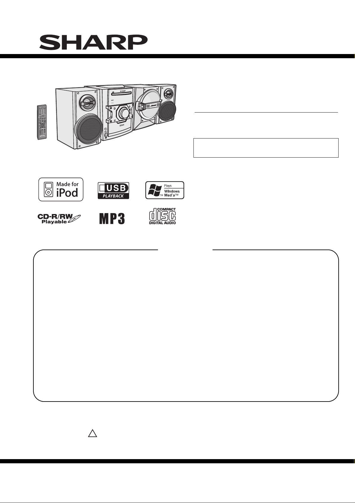
MODEL
CD-SW440N
CD-SW440N Mini Component System consisting of
CD-SW440N (main unit), CP-S440N (speaker system) and
CP-SW440N (subwoofer).
• In the interests of user-safety the set should be restored
to its original condition and only parts identical to those
specified be used.
iPod is a trademark of Apple Inc.,
registered in the U.S. and other countries.
“Made for iPod” means that an electronic accessory has
been designed to connect specifically to iPod and has been
certified by the developer to meet Apple performance
standards.
CONTENTS
PRECAUTIONS FOR USING LEAD-FREE SOLDER
CHAPTER 1. GENERAL DESCRIPTION
[1] Important Service Safety Precaution.............1-1
[2] Important Service Notes (for U.S.A only).......1-1
[3] Specifications ................................................1-2
[4] Name Of Parts...............................................1-3
CHAPTER 2. ADJUSTMENTS
[1] Mechanism Section.......................................2-1
CHAPTER 3. MECHANISM BLOCKS
[1] Caution On Disassembly...............................3-1
CHAPTER 4. DIAGRAMS
[1] Main Block Diagram ......................................4-1
CHAPTER 5. CIRCUIT DESCRIPTION
[1] Waveforms Of Servo Circuit..........................5-1
[2] Voltage...........................................................5-2
Apple is not responsible for the operation of thi
s device or its
compliance with safety and regulatory standards.
CHAPTER 6. CIRCUIT SCHEMATICS AND PARTS
LAYOUT
[1] Notes On Schematic Diagram ....................... 6-1
[2] Types Of Transistor And LED ....................... 6-1
[3] Schematic Diagram........................................ 6-2
[4] Charts Of Connecting Wires ...................... 6-22
[5] Wiring Side Of PWB..................................... 6-24
CHAPTER 7. FLOWCHART
[1] Troubleshooting............................................. 7-1
CHAPTER 8. OTHERS
[1] Function Table Of IC ...................................... 8-1
[2] FL Display...................................................... 8-9
PARTS GUIDE
Parts marked with " " are important for maintaining the safety of the set. Be sure to replace these parts with
!
specified ones for maintaining the safety and performance of the set.
This document has been published to be used
SHARP CORPORATION
for after sales service only.
The contents are subject to change without notice.
Page 2
CD-SW440N
PRECAUTIONS FOR USING LEAD-FREE SOLDER
1.Employing lead-free solder
"MAIN, POWER, DISPLAY/TAPE, SERVO, iPod, FRONT SPEAKER LED, SUBWOOFER LED PWB" of this model
employs lead-free solder. The LF symbol indicates lead-free solder, and is attached on the PWB and service
manuals. The alphabetical character following LF shows the type of lead-free solder.
Examples:
Indicates lead-free solder of tin, silver and copper.
2.
Using lead-free wire solder
When fixing the PWB soldered with the lead-free solder, apply lead-free wire solder. Repairing with conventional
lead wire solder may cause damage or accident due to cracks.
As the melting point of lead-free solder (Sn-Ag-Cu) is higher than the lead wire solder by 40°C, we recommend
you to use a dedicated solder ing bit, if you are not familiar with how to obtain lead-free wire solder or soldering
bit, contact our service station or service branch in your area.
3.
Soldering
As the melting point of lead-free solder (Sn-Ag-Cu) is about 220°C which is higher than the conventional lead
solder by 40°C,and as it has poor solder wettability, you may be apt to keep the soldering bit in contact with the
PWB for extended period of time. However, since the land may be peeled of for the maximum heat-resistance
temperature of parts may be exceeded, remove the bit from the PWB as soon as you confirm the steady
soldering condition.
Lead-free solder contains more tin, and the end of the soldering bit may be easily corrected. Make sure to turn
on and off the power of the bit as required.
If a different type of solder stays on the tip of the soldering bit, it is alloyed with lead-free solder. Clean the bit
after every use of it.
When the tip of the soldering bit is blackened during use, file it with steel wool or fine sandpaper.
Be careful when replacing parts with polarity indication on the PWB silk.
Lead-free wire solder for servicing
Ref No.
PWB-A 92LPWB7792MANS MAIN
PWB-B 92LPWB7792PWRS POWER (B1), DISPLAY/TAPE (B2)
PWB-C RUITKA036AWZZ SERVO
PWB-D 92LPWB7119PODS iPod
PWB-E 92LPWB6514LEDS FRONT SPEAKER LED
PWB-F 92LPWB7285LEDS SUBWOOFER LED
Parts No.
Description
– i –
Page 3
CD-SW440N
CHAPTER 1. GENERAL DESCRIPTION
[1] Important Service Safety Precaution
CAUTION : “These servicing instructions are for use by qualified service personnel only. To reduce
the risk of electric shock do not perform any servicing other than that contained in the operating
instructions unless you are qualified to do so”.
WARNING
1. For continued safety, no modification of any circuit should be attempted.
2. Disconnect AC power before servicing.
CAUTION: FOR CONTINUED
PROTECTION AGAINST FIRE
HAZARD, REPLACE ONLY WITH
SAME TYPE F801, F802 6A, 125V/
F803, F804 2A, 125V/
F805 5A, 125V/
F808 1.6A, 125V FUSES.
ATTENTION: POUR ASSURER
UNE LONGUE PROTECTION CONTRE
UN INCENDIE, REMPLACER SEULEMENT
PAR UN FUSIBLE DE F801, F802 6A, 125V/
F803, F804 2A, 125V/
F805 5A, 125V/
F808 1.6A, 125V FUSES.
[2] Important Service Notes (for U.S.A only)
BEFORE RETURNING THE AUDIO PRODUCT
(Fire & Shock Hazard)
Before returning the audio product to the user,
perform the following safety checks.
1. Inspect all lead dress to make certain that leads
are not pinched or that hardware is not lodged
between
the chassis and other metal parts in the
audio product.
2. Inspect all protective devices such as insulating
materials, cabinet, terminal board, adjustment and
compartment covers or shields, mechanical
insulators etc.
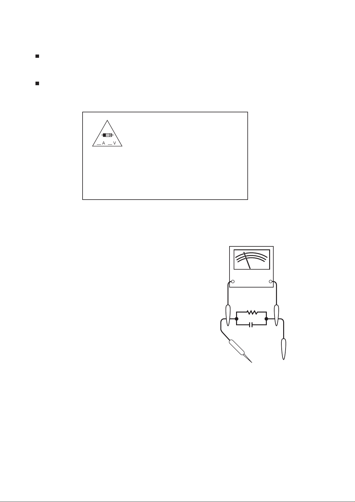
3. To be sure that no shock hazard exists, check for
leakage current in the following manner.
Plug the AC line cord directly into a 120 volt AC
*
outlet.
Using two clip leads, connect a 1.5k ohm, 10
*
watt resistor paralleled by a 0.15µF capacitor in
series with all exposed metal cabinet parts and
a known earth ground, such as conduit or
electrical ground connected to earth ground.
Use a VTVM or VOM with 1000 ohm per volt, or
*
higher, sensitivity to measure the AC voltage drop
across the resistor (See diagram).
Connect the resistor connection to all exposed
*
metal parts having a return path to the chassis
(antenna, metal cabinet, screw heads, knobs and
control shafts, escutcheon, etc.) and measure the
AC voltage drop across the resistor.
VTVM
AC SCALE
1.5k ohms
10W
0.15 µ F
TEST PROBE
TO EXPOSED
METAL PARTS
CONNECT TO
KNOWN EARTH
GROUND
All check must be repeated with the AC line cord plug
connection reversed.
Any reading of 0.3 volt RMS (this corresponds to 0.2
milliamp. AC.) Or more is excessive and indicates a
potential shock hazard which must be corrected before
returning the audio product to the owner.
1 – 1
–2
Page 4
CD-SW440N
[3] Specifications
General
Power source AC 120 V ~ 60 Hz
Power
consumption
Dimensions Width: 9 - 7/16" (240 mm)
Weight 13.9 lbs. (6.3 kg)
102 W
Height: 12 - 7/16" (315.5 mm)
Depth: 11 - 5/32" (283.2 mm)
Amplifier
Output power PMPO: 4500 watts
Output terminals Speakers: 4 ohms
Input terminals Audio In (audio signal):
Front Speakers
RMS: Total 200 watts
(100 watts per channel into 4
ohms at 1 kHz, 10% total
harmonic distortion)
FTC: 75 watts minimum RMS per
channel into 4 ohms from 100
Hz to 20 kHz, 10% total
harmonic distortion.
Subwoofer
RMS: 150 watts into 8 ohms at
70 Hz, 10% total harmonic
distortion
FTC: 130 watts RMS into 8 ohms
from 50 Hz to 120 Hz, 10%
total harmonic distortion.
Headphones: 16 - 50 ohms
(recommended: 32 ohms)
Video output : 1Vp-p
250 mV/47 k ohms
CD player
Type Single disc multi-play compact disc
Signal readout Non-contact, 3-beam
D/A converter Multi bit D/A converter
Frequency
response
Dynamic range 90 dB (1 kHz)
player
semiconductor laser pickup
20 - 20,000 Hz
Cassette deck
Frequency
response
Signal/noise
ratio
Wow and flutter 0.35% (WRMS)
50 - 14,000 Hz (normal tape)
50 dB (playback)
USB
USB host interface Complies with USB 1.1 (Full
Support file MPEG 1 Layer 3
Bitrate support MP3 (32 ~ 320 kbps)
Other Maximum total number of
File system
support
Speed)/ 2.0 Mass Storage
Class.
Support Bulk only and CBI
protocol.
WMA (Non DRM)
WMA (64 ~ 160 kbps)
MP3/WMA files is 1024.
Maximum total number of
folders is 255 INCLUSIVE of
root directory.
The ID3TAG information
supported are TITLE, ARTIST
and ALBUM only.
Supports ID3TAG version 1
and version 2.
Support USB devices with
Microsoft Windows/DOS/FAT
12/ FAT 16/ FAT 32.
2 kbyte block length for sector.
Tuner
Frequency range FM: 87.5 - 108 MHz
AM: 530 - 1,720 kHz
Speaker
Front Speaker
Type
Maximum input
power
Rated input power 100 W
Impedance 4 ohms
Dimensions Width: 7-1/16" (180 mm)
Weight 6.0 lbs. (2.7 kg)/each
Subwoofer
Type Subwoofer system
Maximum input
power
Rated input power 150 W
Impedance 8 ohms
Dimensions Width: 9-1/16" (230 mm)
Weight 9.7 lbs. (4.4 kg)
2-way type speaker system
2" (5 cm) tweeter
5-1/8" (13 cm) woofer
200 W
Height: 11-13/16" (300 mm)
Depth: 8" (204 mm)
8" (16 cm) woofer
300 W
Height: 11-13/16" (300 mm)
Depth: 12" (305 mm)
1 – 2
– 4
Page 5
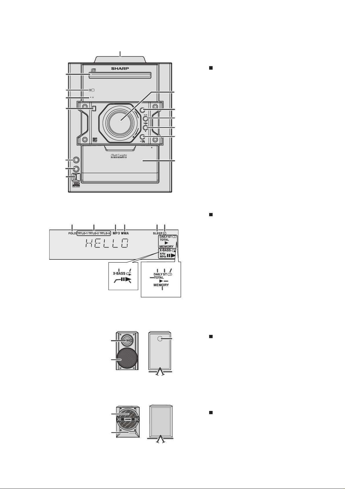
[4] Names Of Parts
FUNCTION
AUDIOIN
PHONES
VOL
POWER
ON/STAND-BY
PUSH
OPEN
2
3
4
5
AUDIO IN
6
PHONES
7
8
POWER
ON/STAND-BY
1
MINI COMPONENT SYSTEM
CD-DH790
VOL
FUNCTION
CD-SW440N
Front panel
1. iPod Docking Station
2. Disc Tray
9
10
11
12
13
PUSH
OPEN
14
3. Remote Sensor
4. Timer Indicator
5. Power On/Stand-by Button
6. Audio In Jack
7. Headphone Jack
8. USB Terminal
9. Volume Control
10. FUNCTION Button
11. Disc / USB / iPod Play or Pause / Tape Play /
Tuning Up Button
12. Disc / USB / Tape Stop / Tuning Down Button
13. Disc Tray Open / Close Button
14. Cassette Compartment
1234 5
13 14
7
15
16
6
8910
11
12
1
2
Display
1. MP3/WMA Folder Indicator
2. MP3/WMA Title Indicators
3. MP3 Indicator
4. WMA Indicator
5. Sleep Indicator
6. Once Timer Play Indicator
7. MP3/WMA Total Indicator
8. Daily Timer Play Indicator
9. FM Stereo Mode Indicator
10. FM Stereo Receiving Indicator
11. Tape play Indicator
12. Memory Indicator
13. Extra Bass Indicator
14. Disc/USB Repeat Play Indicator
15. Disc/USB Pause Indicator
16. Disc/USB Play Indicator
3
Front speaker system
1. Tweeter
2. Woofer
3. Bass Reflex Duct
4. Speaker Wire
5. Speaker Light-Up Wire
54
1
Subwoofer
1. Subwoofer
2. Bass Reflex Duct
2
3 4
1 – 3
–2
3. Subwoofer Light-Up Wire
4. Speaker Wire
Page 6
CD-SW440N
1
22
2
3
4
5
6
7
8
9
10
11
12
CD
USB
23
24
25
26
27
28
29
30
13
14
15
16
17
18
19
20
TAPE
31
32
33
34
35
21
36
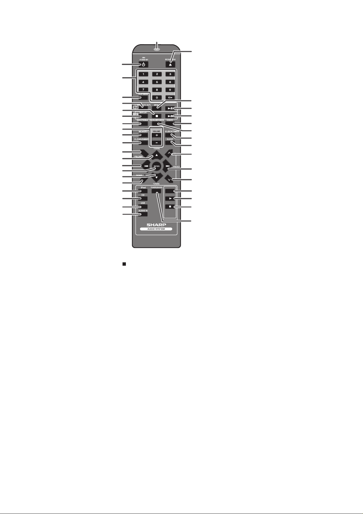
Remote control
1. Remote Control Transmitter
2. On/Stand-by Button
3. Direct Search Buttons
4. Play Mode Button
5. iPod Display (TV OUT) Button
6. Disc/USB Stop Button
7. Disc/USB Display Button
8. Bass/Treble Button
9. Volume Up or Down Buttons
10. Memory Button
11. Clear/Dimmer Button
12. Folder Button
13. Tuning Up, iPod Cursor Up Button
14. CD Track Down or Fast Reverse, Time Down Button
15. Enter Button
16. Tuning Down, iPod Cursor Down Button
17. Demo Button
18. iPod Button
19. Disc Button
20. USB Button
21. Audio In Button
22. Open/Close Button
23. iPod Menu Button
24. iPod Play/Pause Button
25. Disc/USB Play/Pause Button
26. X-Bass Button
27. Equaliser Mode Button
28. Clock/Timer Button
29. Sleep Button
30. Tuner Preset Up Button
31. CD Track Up or Fast Forward, Time Up Button
32. Tuner Preset Down Button
33. Tape Button
34. Tape Play Button
35. Tape Stop Button
36. Tuner (Band) Button
1 – 4
– 4
Page 7
CD-ES700/CD-ES77CD-ES700/CD-ES77Service ManualCD-ES700/CD-ES77MarketE
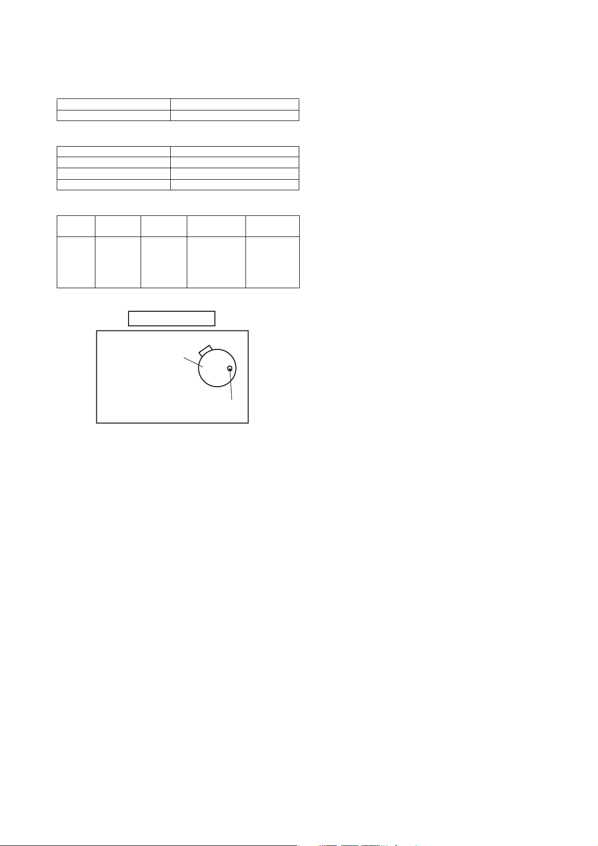
CHAPTER 2. ADJUSTMENTS
[1] Mechanism Section
• Driving Force Check
Torque Meter Specified Value
Play: TW-2111 Tape 1: Over 90 g
• Torque Check
Torque Meter Specified Value
Play: TW-2111 29 to 75 g.cm
Fast Forward: TW-2231 55 to 170 g.cm
Rewind: TW-2231 55 to 170 g.cm
• Tape Speed
CD-SW440N
Test Tape Adjusting
Normal
speed
Figure 1
MTT-111 Variable
Point
Resistor in
motor.
TAPE MECHANISM
Tape Motor
Variable Resistor in motor
Specified
Value
3,000 ± 90 Hz
Speaker
Instrument
Connection
Speaker
Terminal
(Load
resistance:
6 ohms)
2 – 1
Page 8
CD-SW440N
CD-ES700/CD-ES77CD-ES700/CD-ES77Service ManualCD-ES700/CD-ES77MarketE
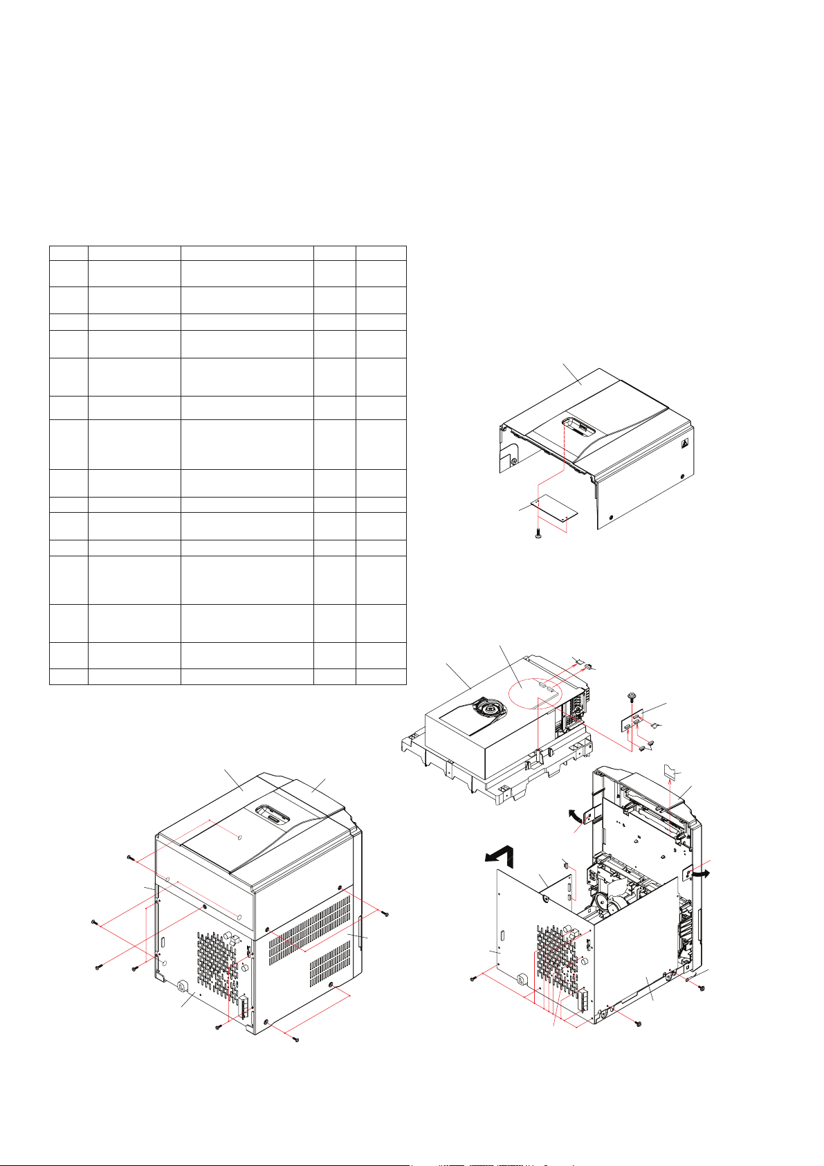
CHAPTER 3. MECHANISM BLOCKS
[1] Caution On Disassembly
Follow the below-mentioned notes when disassembling the unit and reassembling it, to keep it safe and ensure
excellent performance:
1. Take cassette tape and compact disc out of the unit.
2. Be sure to remove the power supply plug from the wall outlet before starting to disassemble the unit.
3. Take of f nylon ba nds or wire ho lders wh ere the y n eed to be re moved when disassemb ling th e unit. After servicing
the unit, be sure to rearrange the leads where they were before disassembling.
STEP REMOVAL PROCEDURE FIGURE
.........
(A1)x5
(A2)x1
(B1)x8 1
(C1)x2 2
(D1)x1
(D2)x2
(E1)x2
(E2)x1
(E3)x1
(F1)x9 3
(G1)x2
(G2)x2
(G3)x4
(G4)x2
(H1)x4
(H2)x1
(J4)x4 4
(K1)x6
(K2)x1
(L1)x1 6
(M1)x1
(M2)x1
(M3)x1
(M4)x4
(N1)x2
(N2)x2
(N3)x1
(P1)x4
(P2)x1
(Q1)x4 9
1 Top Cabinet
Side Panel (Left/
2
Right)
iPod PWB
3
4 iPod Transit PWB
5 CD Changer unit
Rear Panel with
6
Fan motor
7 Front Panel
8Main PWB
9Power PWB
10 Tape Mechanism
11 Audio In PWB
12 Display PWB
13 CD PWB
Changer
14
Mechanism Unit
15 CD Mechanism
..........................
1. Screw
2. Flat Cable....................
2. Screw
..........................
..........................
1. Screw
..........................
1. Screw
2. Socket
1. Hook
2. Socket
3. Flat Cable
1. Screw
1. Screw
2. Flat Cable
3. Socket
4. Hook
1. Screw
2. Socket
1. Screw
1. Screw
2. Flat Cable
1. Screw
1. Knob
2. Nut
3. Washer
4. Screw
1. Screw
2. Flat Cable
3. Socket
1. Screw
.........................
...........................
..........................
.....................
...........................
..........................
...................
........................
...........................
..........................
.........................
..........................
..........................
....................
..........................
...........................
..............................
........................
..........................
..........................
....................
.........................
..........................
2. Changer Chassis
1. Screw
..........................
Note:
After removing the connector for the optical pickup from the connector,
wrap the conductive aluminium foil around the front end of the connector
so as to protect the optical pickup from electrostatic damage.
Top Cabinet
Front Panel
4
3,4
3,4
4
3, 4
4
1
3
3
3
5
6
7
8
CD Changer Unit
iPod PWB
M3 x 10mm
CD Servo PWB
Top Cabinet
(C1) x 2
Figure 2
(E3) x 1
(E2) x 1
(D1) x 1
Special Screw
iPod
Transit PWB
(A2) x 1
(D2) x 2
(G2) x 1
Front Panel
(B1) x 2
M3 x 10mm
(A1) x 1
M3 x 12mm
(A1) x 2
M3 x 12mm
Side Panel
(Right)
(B1) x 2
M3 x 10mm
Figure 1
Rear Panel
(B1) x 2
M3 x 10mm
(B1) x 2
M3 x 10mm
(A1) x 2
M3 x 12mm
Side Panel (Left)
3 – 1
Rear Panel
(F1) x 9
M3 x 10mm
PULL
(E1) x 1
(G3) x 1
Power PWB
Fan Motor
Figure 3
Hook
Main PWB
(H1) x 1
Special Screw
Hook
(E1) x 1
PULL
Lug wire
(H1) x 1
Special Screw
Page 9
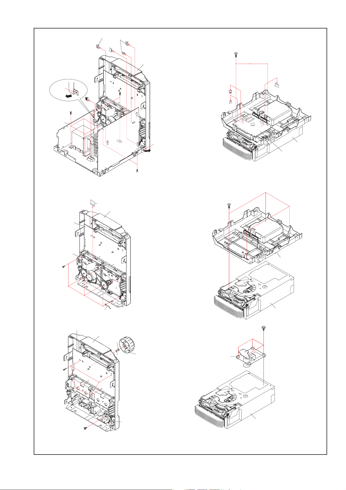
CD-SW440N
Hook
(G4) x 1
PULL
Power PWB
(J1) x 4
M4 x 8mm
Figure 4
(H2) x 1
(G3) x 1
(K2) x 1
(G2) x 1
(H1) x 2
M3 x 6mm
Front Panel
(G3) x 2
Front Panel
(G1) x 2
M3 x 8mm
Hook
(G4) x 1
PULL
(N3) x 1
(N2) x 1
(P1) x 4
M3 x 10mm
Figure 7
(N1) x 2
M3 x 10mm
(N2) x 1
CD PWB
Changer
Mechanism
Unit
Display PWB
Mechanism
(K1) x 6
M3 x 10mm
(M4) x 4
M2.6 x 10mm
Tap e
Figure 5
Display PWB
Lug wire
Front Panel
(M2) x 1
(M3) x 1
(M1) x 1
Figure 8
CD Mechanism
(Q1) x 4
Special
(P2) x 1
Changer
Mechanism
Unit
(L1) x 1
Special Screw
Figure 6
Audio In PWB
3 – 2
Figure 9
Changer
Mechanism
Unit
Page 10
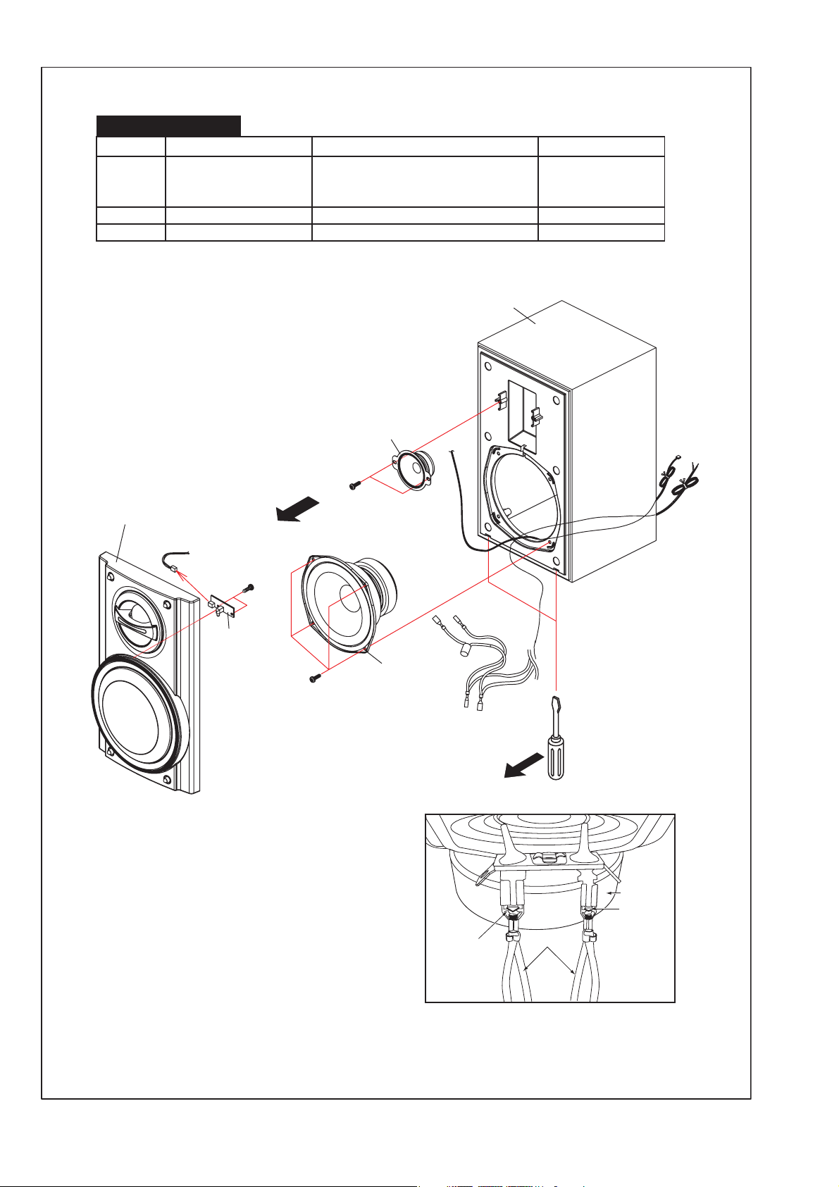
CD-SW440N
CP-S440N
REMOVAL
LED PWB
2. Socket…….…………..… (A2)X1
3. Screw…….…….…….…. (A3)X2
2 Woofer 1. Screw…….…….…….…. (B1)X4 10
3 Tweeter 1. Screw…….……….....…. (C1)X2 10
PROCEDURE
………Front Panel Assy .11 … (A1)X1 10
Speaker Box
ERUGIFPETS
Front Panel Ass’y
(A1) x 1
(A2) x 1
FROM BOX ASSY
(A3 ) x 2
M3 x 10mm
LED PWB
(C1) x 2
M3 x 10mm
(B1) x 4
M4 x 16mm
Figure 10
Tweeter
Woofer
LED PWB
TO
Screwdriver
SPEAKER UNIT
LOCKING TAB
LOCKING TAB
CAUTION:
TO REMOVE SPEAKER UNIT, PRESS THESE LOCKING TABS
TO RELEASE SPEAKER WIRES.
SPEAKER WIRE
3 – 3
Page 11
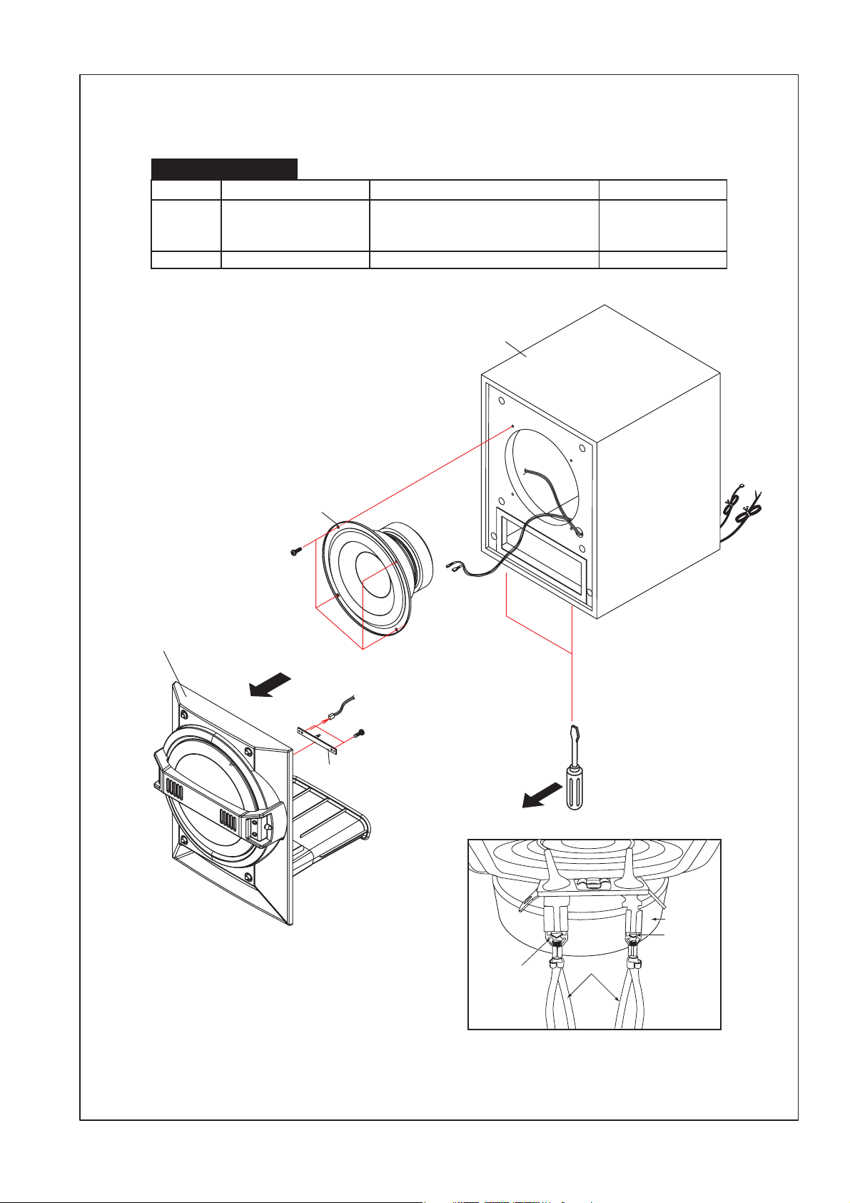
CP-SW440N
PROCEDUREREMOVAL
1 LED PWB 1. Front Panel Assy…………(A1)X1 11
2. Socket…….…………..… (A2)X1
3. Screw…….…….…….…. (A3)X2
2 Woofer 1. Screw…….…….…….…. (B1)X4 11
Speaker Box
TO
LED
PWB
CD-SW440N
ERUGIFPETS
(A1) x 1
Front Panel Ass’y
(B1) x 4
M4 x 16mm
Subwoofer
LED PWB
(A2) x 1
FROM BOX ASSY
(A3) x 2
M2.6 x 8mm
Screwdriver
SPEAKER UNIT
LOCKING TAB
Figure 11
3 – 4
LOCKING TAB
CAUTION:
TO REMOVE SPEAKER UNIT, PRESS THESE LOCKING TABS
TO RELEASE SPEAKER WIRES.
SPEAKER WIRE
Page 12
CD-SW440N
V
V
5
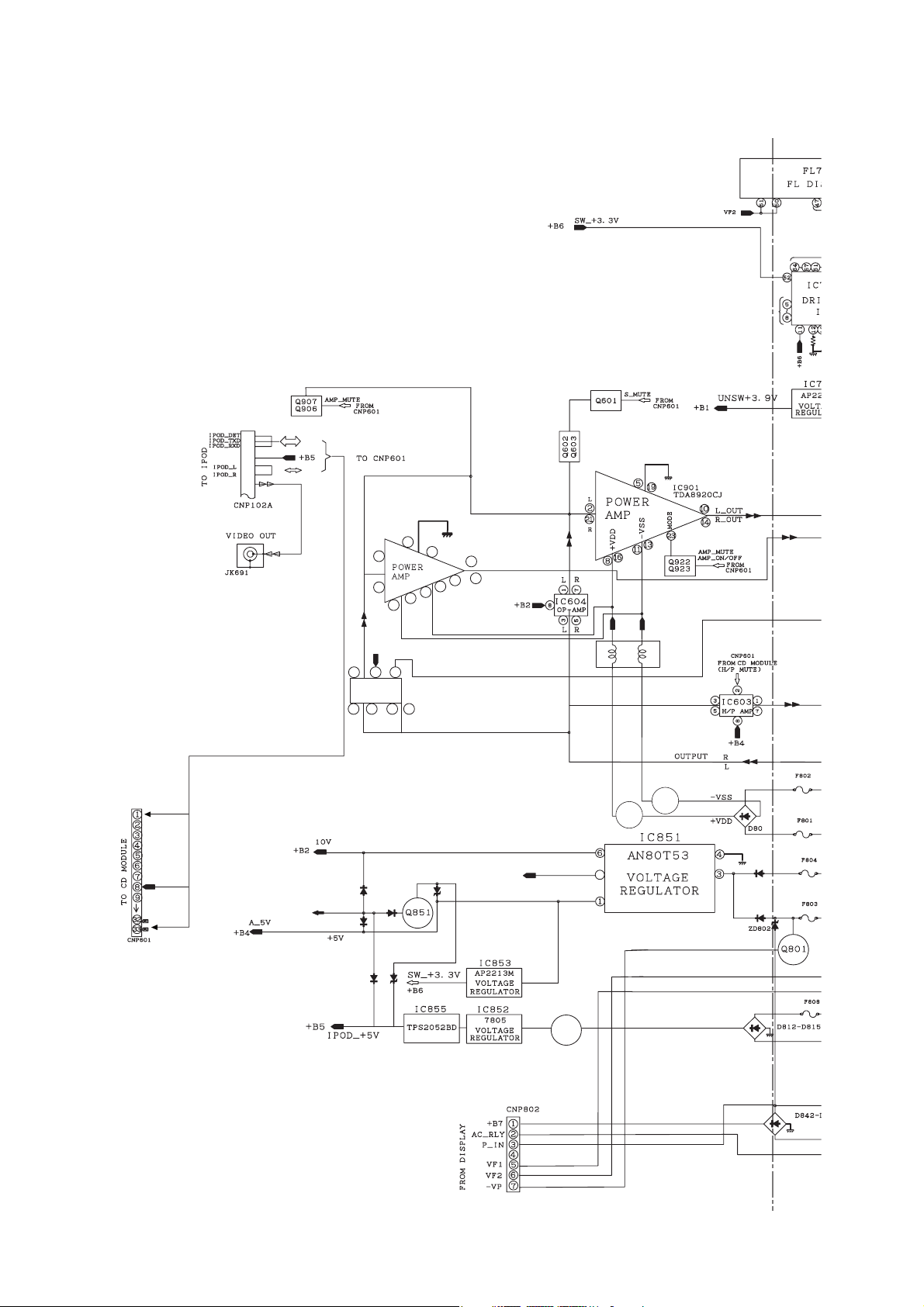
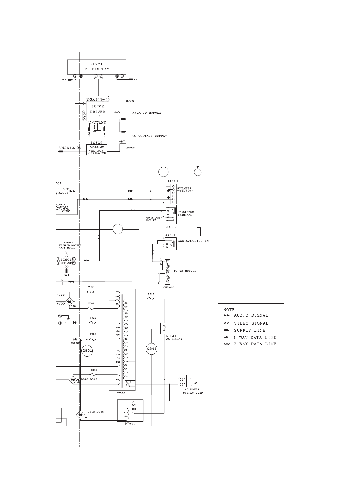
CHAPTER 4. DIAGRAMS
[1] Main Block Diagram
SYS_PROTECT
5
2
21
+
16
8
+B3
1
87
IC503
23 56
19
10
L_OUT
R_OUT
4
23
-
13
11
L927
+13V
+B3
R
L
Q905
Q901
2
R
L
6A 125V
6A 125V
2
2A 125
2A 125
Q852
Figure 4-1: MAIN BLOCK DIAGRAM (1/2)
4 – 1
1.6A 12
Page 13
+B3
CD-SW440N
Q906
Q503
R
L
6A 125V
6A 125V
2
2A 125V
2A 125V
14
12
17
15
5A 125V
7
M FAN MOTOR
CNP300N302
SPEAKER
LED
1.6A 125V
8
9
10
11
3
L844
ZA016AW
120V ~ 60Hz
Figure 4-2: MAIN BLOCK DIAGRAM (1/2)
4 – 2
Page 14
CD-SW440N
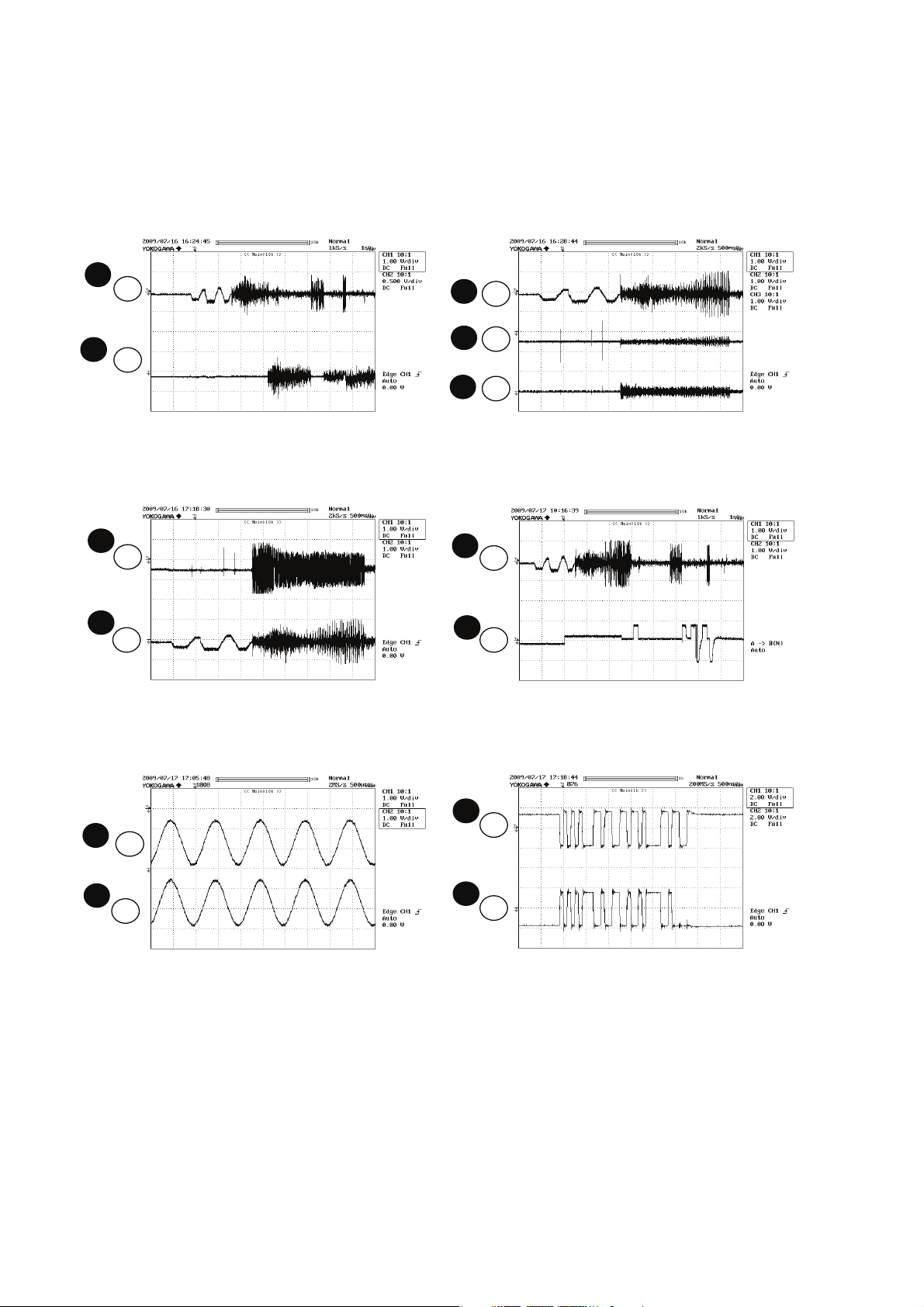
CHAPTER 5.
CIRCUIT DESCRIPTION
[1] Waveforms Of Servo Circuit
1
U10 U10
2
U10
126
127
FOO
TRO
Figure 1 Figure 2
1
3
U10
4
FOO
126
FE
13
TE
14
U10
4
TE
14
U10 U10
1
FOO
126
U10 U10
Figure 3 Figure 4
LINEOUTL
6
33
U10
7
36
U10 U10
LINEOUTR
Figure 5 Figure 6
1
126
5
123
9
FOO
DMO
DM
52
U10
10
53
DP
5 – 1
RFO
Page 15
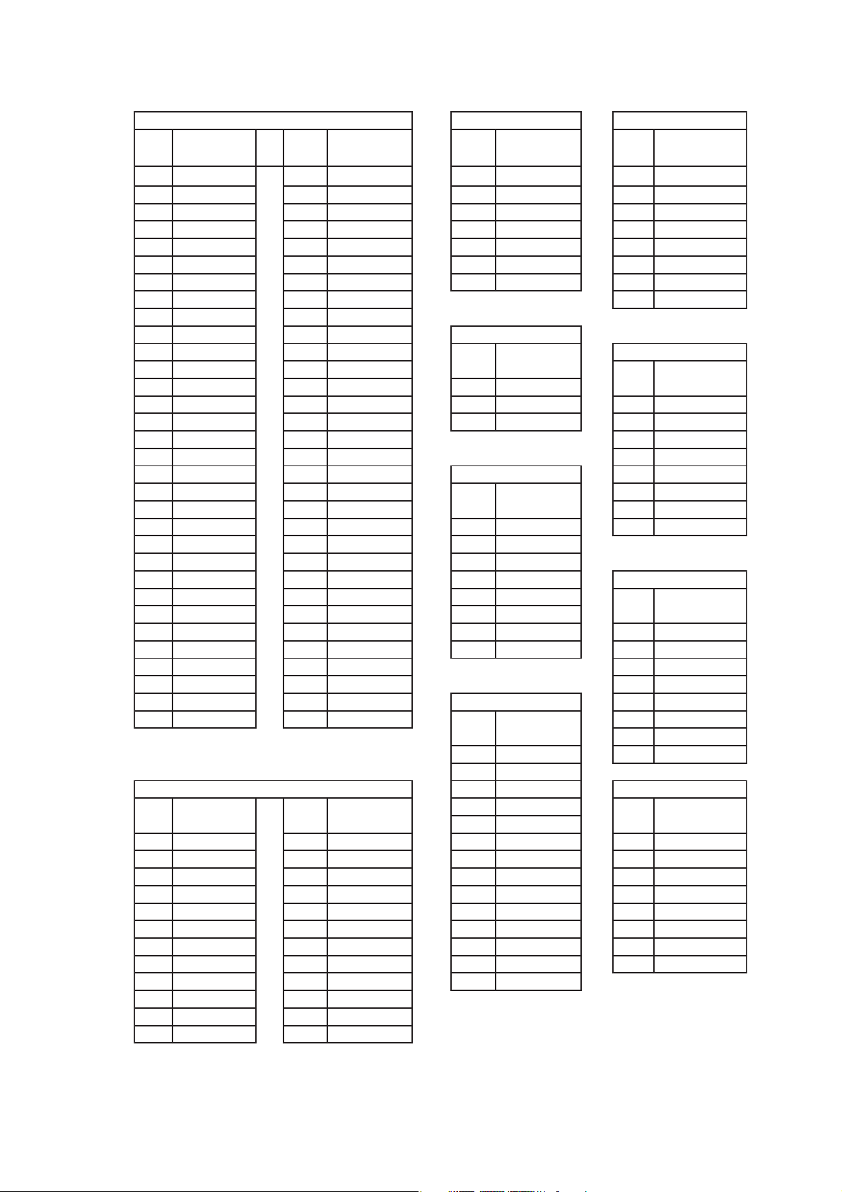
[2] Voltage
IC701 IC851 IC702
PINNOVOLTAGE
(V)
1 -26.66 33 -26.68 1 5.12 1 12.13
2 -26.66 34 -29.10 2 13.03 2 12.23
3 -26.66 35 -26.68 3 18.53 3 3.79
4 -26.66 36 -21.10 4 0.00 4 2.49
5 3.15 37 -17.68 5 19.65 5 0.50
6 3.15 38 -22.10 6 10.05 6 0.50
7 3.06 39 -29.10 7 8.51 7 0.50
8 3.15 40 -24.25 8 0.50
9 3.15 41 -19.40
10 3.15 42 -26.66
11 3.15 43 -24.25
12 1.45 44 -24.57
13 1.45 45 -24.27 1 11.05
14 0.00 46 -19.43 2 0.69 1 5.10
15 -17.50 47 -26.68 3 5.70 2 5.06
16 -29.09 48 -26.68 3 4.94
17 -29.10 49 -29.10 4 0.00
18 -29.10 50 -22.10
19 -29.10 51 -22.10 6 5.06
20 -29.10 52 3.15 7 5.09
21 -29.10 53 -29.10 1 5.12 8 10.04
22 -26.90 54 -29.10 2 5.12
23 -15.26 55 -29.10 3 3.29
24 -29.25 56 -29.10 4 1.92
25 -29.10 57 -26.68 5 0.00
26 -29.10 58 -26.68 6 0.00
27 -19.75 59 -26.68 7 0.00 1 2.02
28 -29.10 60 -26.68 8 0.00 2 2.02
29 -19.70 61 -26.68 3 2.02
30 -21.84 62 -26.68 4 0.00
31 -19.55 63 -26.68
32 -15.23 64 -26.68 6 2.02
PINNOVOLTAGE
(V)
1 2.53 13 -24.48 6 2.52 1 0.50
2 0.00 14 0.00 7 0.00 2 5.70
3 2.44 15 11.45 8 5.12 3 3.16
4 24.15 16 24.35 9 0.00 4 0.00
5 0.00 17 -24.29 10 2.54 5 3.17
6 -24.08 18 -24.15 11 2.57 6 5.09
7 -15.95 19 0.00 12 5.12 7 5.70
8 24.17 20 24.09 13 0.00 8 3.17
9 11.46 21 0.00 14 5.12
10 0.00 22 0.00
11 -24.38 23 2.67
12 -12.10
PINNOVOLTAGE
IC901
PINNOVOLTAGE
(V)
(V)
PINNOVOLTAGE
(V)
IC852
PINNOVOLTAGE
(V)
IC853
PINNOVOLTAGE
(V)
IC902
PINNOVOLTAGE
(V)
1 0.00 8 5.12
2 5.12
3 2.52
4 2.57
5 2.42
PINNOVOLTAGE
IC604
PINNOVOLTAGE
5 4.94
IC603
PINNOVOLTAGE
5 2.02
7 2.04
IC855
PINNOVOLTAGE
(V)
(V)
(V)
(V)
CD-SW440N
5 – 2
Page 16
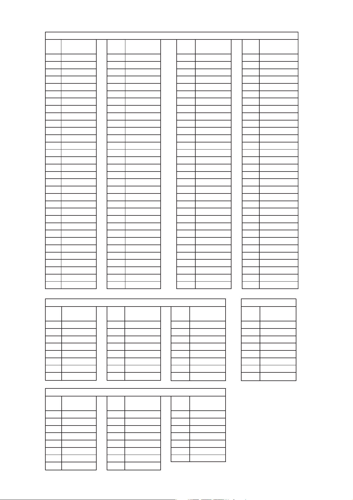
CD-SW440N
PINNOVOLTAGE
U10
PIN
(V)
1 3.38 33 1.53 65 1.23 97 NC
2 1.79 34 1.53 66 NC 98 NC
3 1.58 35 1.53 67 NC 99 0.71
4 1.60 36 1.53 68 NC 100 NC
5 1.60 37 0.00 69 NC 101 NC
6 1.60 38 3.34 70 141m 102 NC
7 1.60 39 NC 71 0.00 103 1.25
8 3.39 40 NC 72 NC 104 0.72
9 1.59 41 NC 73 NC 105 0.72
10 1.19 42 NC 74 NC 106 NC
11 0.00 43 NC 75 NC 107 NC
12 1.12 44 NC 76 NC 108 NC
13 1.18 45 0.77 77 NC 109 NC
14 1.38 46 1.53 78 NC 110 0.00
15 0.81 47 0.77 79 NC 111 5.80
16 3.34 48 1.53 80 NC 112 0.00
17 3.34 49 1.72 81 NC 113 3.34
18 1.79 50 2.11 82 NC 114 0.00
19 1.67 51 2.08 83 NC 115 1.77
20 2.31 52 30.4m 84 0.00 116 3.34
21 0.00 53 2.82 85 3.34 117 NC
22 0.00 54 3.34 86 0.72 118 NC
23 3.33 55 0.00 87 NC 119 NC
24 1.78 56 0.00 88 NC 120 1.58
25 3.34 57 3.34 89 NC 121 1.57
26 1.27 58 0.00 90 NC 122 3.34
27 0.72 59 2.19 91 NC 123 1.57
28 0.00 60 0.00 92 1.30 124 0.00
29 1.77 61 0.41 93 1.13 125 NC
30 0.00 62 3.34 94 0.71 126 1.57
31 1.53 63 3.34 95 0.71 127 1.57
32 1.53 64 1.22 96 NC 128 233m
NO
VOLTAGE
(V)
PIN
NO
VOLTAGE
(V)
PIN
NO
VOLTAGE
(V)
IC401 IC503
PINNOVOLTAGE
(V)
1 0.00 9 0.00 17 25.80m
2 0.00 10 200.10m 18 0.00
3 0.00 11 0.00 19 0.00
4 0.78 12 0.00 20 2.80
5 2.79 13 6.87 21 0.77
6 0.00 14 4.13 22 0.00
7 0.00 15 0.00 23 0.00
8 25.80m 16 0.00 24 0.00
PINNOVOLTAGE
(V)
1 2.53 9 11.46 17
2 0.00 10 0.00 18
3 2.44 11 -24.38 19
4 24.15 12 -12.10 20
5 0.00 13 -24.48 21
6 -24.08 14 0.00 22 0.00
7 -15.95 15 11.45 23 2.67
8 24.17 16 24.35
PINNOVOLTAGE
(V)
IC301
PINNOVOLTAGE
(V)
PINNOVOLTAGE
(V)
PINNOVOLTAGE
(V)
-24.29
-24.15
0.00
24.09
0.00
PINNOVOLTAGE
(V)
1 6.11
2 6.11
3 6.05
4 0.00
5 1.64
6 1.65
7 1.64
8 12.19
5 – 3
Page 17
CD-SW440N
CHAPTER 6. CIRCUIT SCHEMATICS AND PARTS LAYOUT
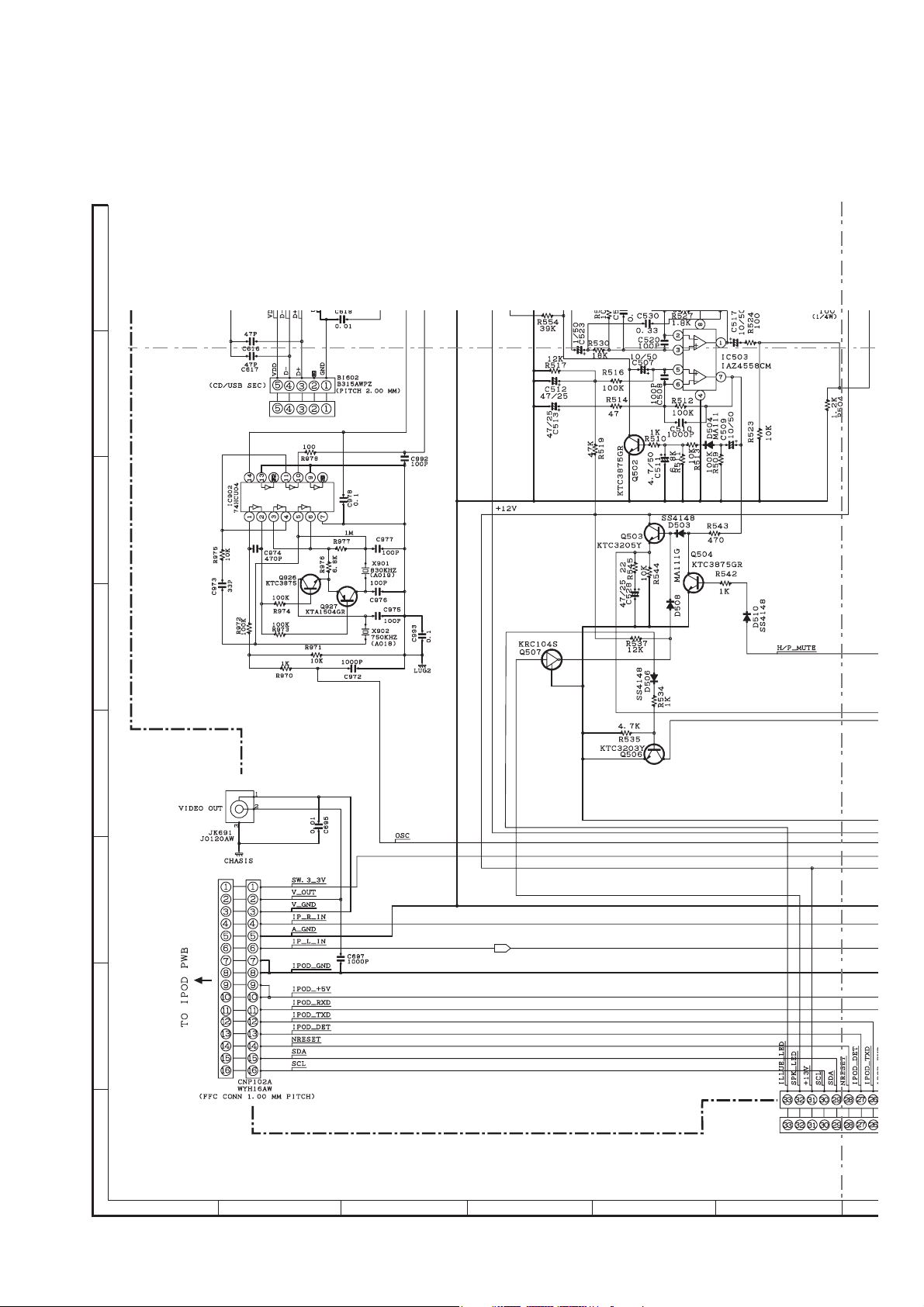
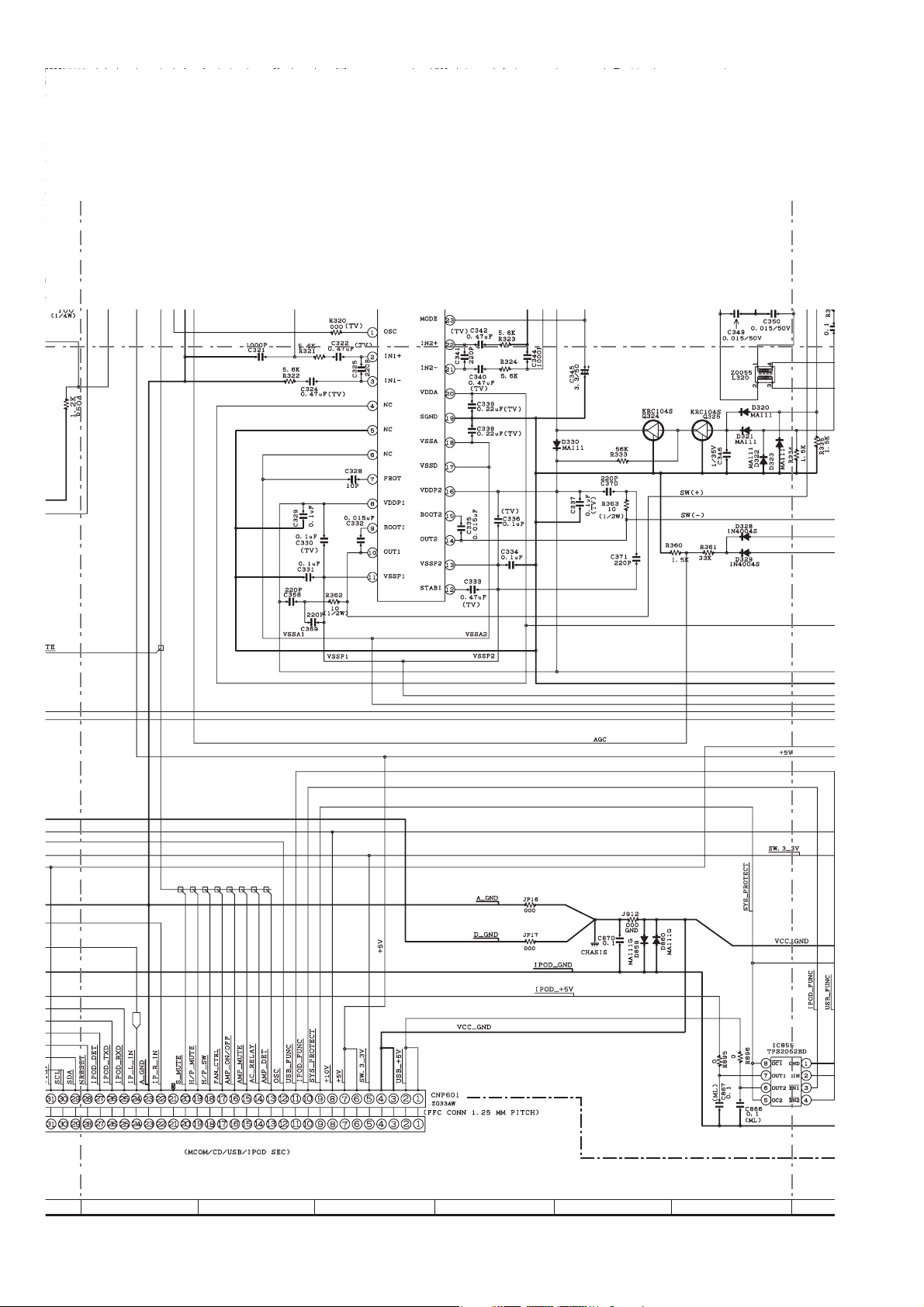
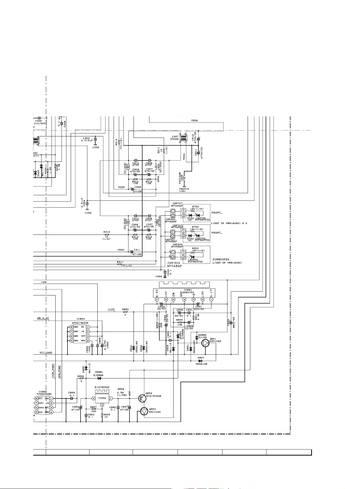
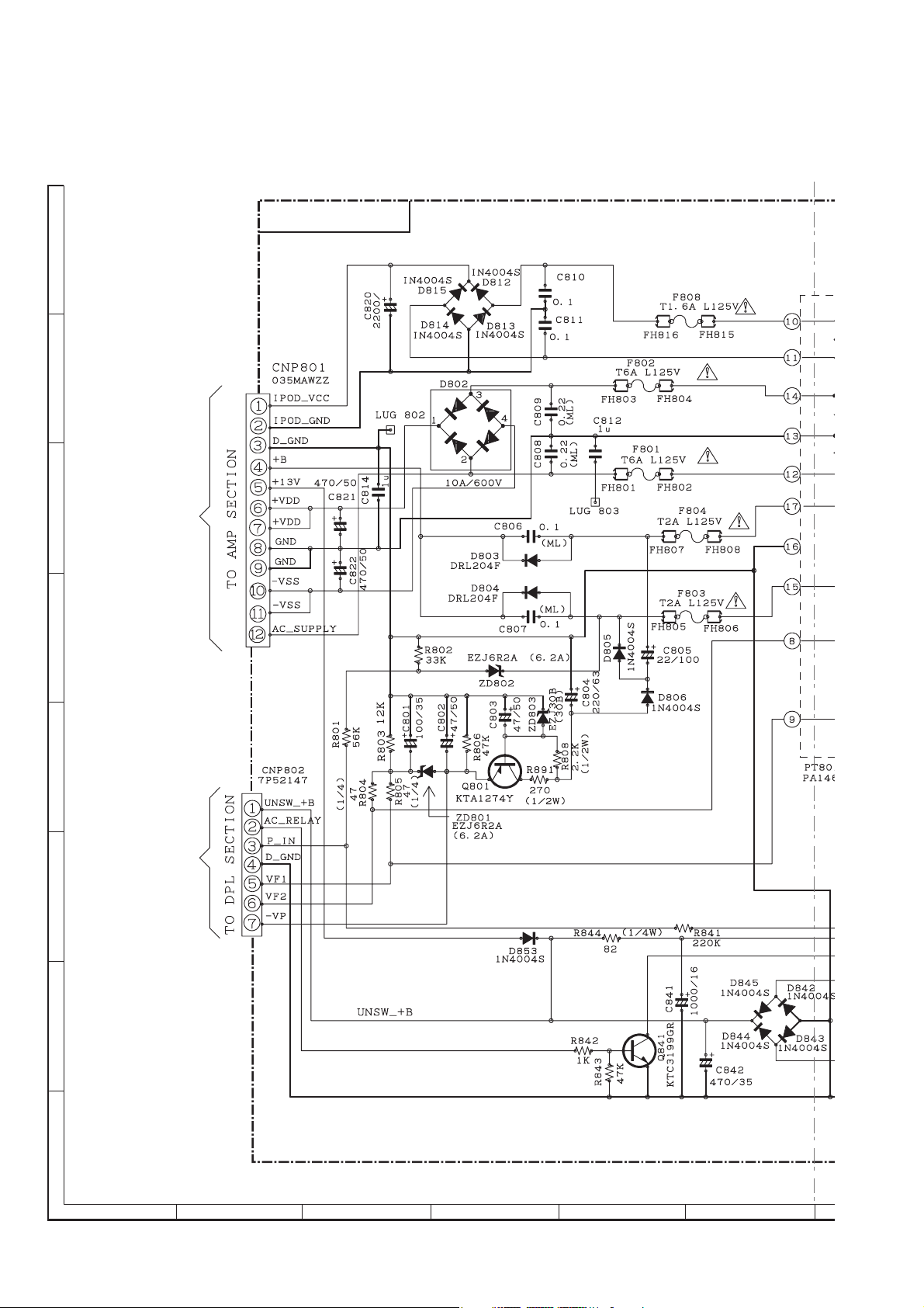
[1] Notes On Schematic Diagram
• Resistor:
To differentiate the units of resistors, such symbol as K and M are
used: the symbol K means 1000 ohm and the symbol M means
1000 kohm and the resistor without any symbol is ohm-type resistor. Besides, the one with “Fusible” is a fuse type.
• Capacitor:
To indicate the unit of capacitor, a symbol P is used: this symbol P
means pico-farad and the unit of the capacitor without such a symbol is microfarad. As to electrolytic capacitor, the expression
"capacitance/withstand voltage is used".
(CH), (TH), (RH), (UJ): Temperature compensation
(ML): Mylar type
(P.P.): Polypropylene type
REF. NO
VR701 VOLUME MAX -- MIN
SW701 ON/STAND-BY ON -- OFF
SW702 FUNCTION ON -- OFF
SW703 DISC/USB/TAPE STOP/TUNING DOWN ON -- OFF
SW704 DISC/USB/iPod PLAY or PAUSE/
TAPE PLAY/TUNING UP
SW705 OPEN/CLOSE ON -- OFF
DESCRIPTION POSITION
ON -- OFF
• Schematic diagram and Wiring Side of P.W.Board for this model are
subject to change for improvement without prior notice.
• The indicated voltage in each section is the one measured by Digital Multimeter between such a section and the chassis with no signal given.
1. In the tuner section,
indicates AM
indicates FM stereo
2. In the main section, a tape is being playback.
3. In the power section, a tape is being playback.
4. In the CD section, the CD is stopped.
Parts marked with “ ” ( ) are important for main-
•
taining the safety of the set. Be sure to replace these parts with
specified ones for maintaining the safety and performance of the
set.
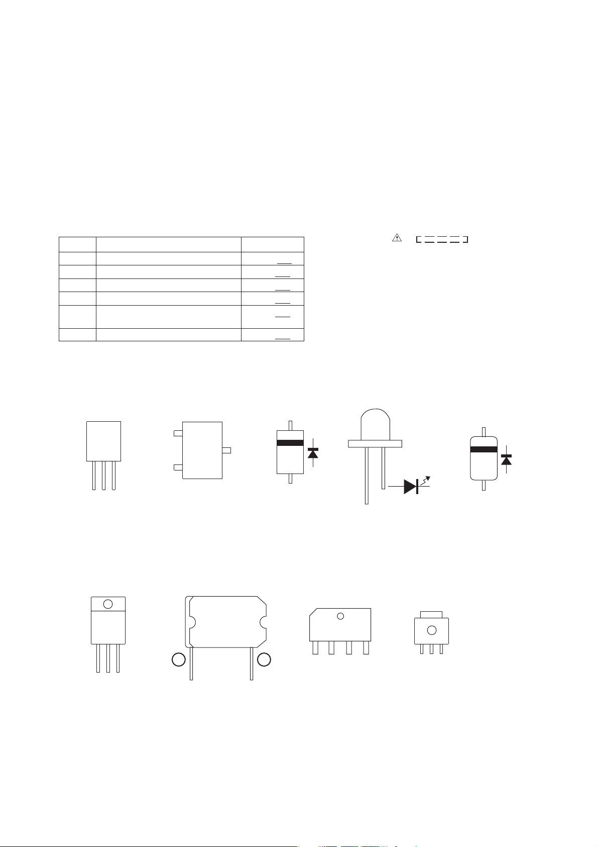
[2] Typ es Of Transistor And LED
FRONT
VIEW
ECB
(S)(G)(D)
(1)(2)(3)
S8550
KTA1274Y
S8050
KTC3199
KTA1266
KTC3203Y
FRONT
VIEW
BCE
B772
KIA7805A
050N60P
B
(3)
E
(1)
TOP
VIEW
KRA102S
KRC107
KRC104S
H1A
KTA1504GR
KTC3875GR
KRA107S
1
TDA8920CJ
FRONT
VIEW
(2)
TOP VIEW
C
TOP VIEW
FRONT
VIEW
23
1N4004
DRL204F
MA 111
FRONT
VIEW
AC AC -+
10XB60F
343VC3F
TOP VIEW
BCE
HD
HSS4148
6 – 1
Page 18
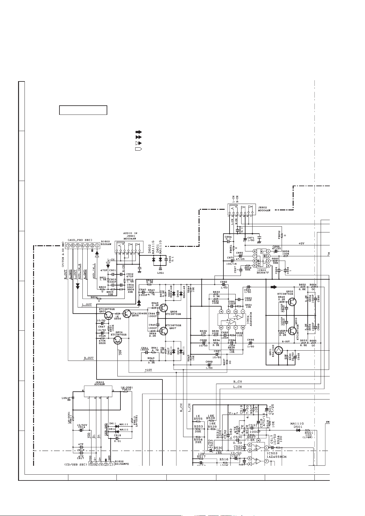
CD-SW440N
[3] Schematic Diagram
A
MAIN PWB-A
FM SIGNAL
CD SIGNAL
AUDIO SIGNAL
iPod SIGNAL
B
HEADPHONES IN
C
TO SERVO PWB
C875
0.1
LUG1
D
JP24
0.1
LUG1
E
F
USB IN
G
H
1
TO SERVO PWB
23456
Figure 6-1: MAIN SCHEMATIC DIAGRAM (1/6)
6 – 2
Page 19
CD-SW440N
7
8 9 10 11 12
Figure 6-2: MAIN SCHEMATIC DIAGRAM (2/6)
6 – 3
Page 20
CD-SW440N
FAN
MOTOR
TO
SPEAKER SYSTEM
13
14 15 16 17 18
Figure 6-3: MAIN SCHEMATIC DIAGRAM (3/6)
6 – 4
Page 21
CD-SW440N
USB IN
A
TO SERVO PWB
B
C
D
E
F
G
H
1
23456
Figure 6-4: MAIN SCHEMATIC DIAGRAM (4/6)
6 – 5
Page 22
CD-SW440N
TO SERVO PWB
7
8 9 10 11 12
Figure 6-5: MAIN SCHEMATIC DIAGRAM (5/6)
6 – 6
Page 23
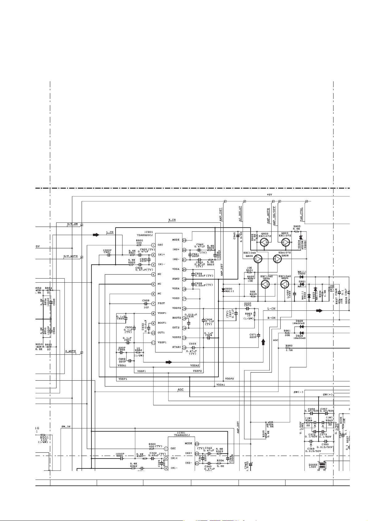
CD-SW440N
L-CH
R-CH
13
14 15 16 17 18
Figure 6-6: MAIN SCHEMATIC DIAGRAM (6/6)
6 – 7
Page 24
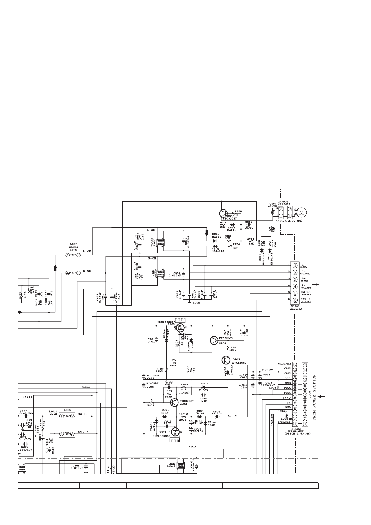
CD-SW440N
A
B
POWER PWB-B1
25V
C
D
E
F
G
H
1
23456
Figure 6-7: POWER SCHEMATIC DIAGRAM (1/2)
6 – 8
Page 25
CD-SW440N
AC POWER SUPPLY CORD
AC 120V ~ 60Hz
7
8 9 10 11 12
Figure 6-8: POWER SCHEMATIC DIAGRAM (2/2)
6 – 9
Page 26
CD-SW440N
A
B
DISPLAY/TAPE PWB-B2
C
D
E
F
FROM SERVO PWB
G
H
1
23456
Figure 6-9: DISPLAY/TAPE SCHEMATIC DIAGRAM (1/2)
6 – 10
Page 27
CD-SW440N
7
8 9 10 11 12
Figure 6-10: DISPLAY/TAPE SCHEMATIC DIAGRAM (2/2)
6 – 11
Page 28

CD-SW440N
A
B
PLAYBACK SIGNAL
DISPLAY/TAPE PWB-B2
C
D
E
F
TO SERVO PWB
G
H
1
23456
Figure 6-11: DISPLAY/TAPE SCHEMATIC DIAGRAM (1/2)
TO SERVO PWB
6 – 12
Page 29

CD-SW440N
7
8 9 10 11 12
Figure 6-12: DISPLAY/TAPE SCHEMATIC DIAGRAM (2/2)
6 – 13
Page 30

CD-SW440N
C5001uF
4
F
T3V3
A
SERVO PWB-C
FMI
10K(NC)
R61 10K
R60
30pF
C47
T1
R59 10K(NC)
10K(NC)
R6210K(NC)
R6310K
R64
XIN
AMI
NC
LOUT
ROUT
SEN7SCLK8SDIO9RCLK10VIO
6
C54
22pF
GND
16NC17P318P219P120
15
NC
14
13
12
GND
11
VDD
21
GND
R72 10K(NC)
10R
Y3
32.768K
R74
GND
EC4220uF
GND
C53
22pF
B
T3V3
AMT
C115
10K(NC)
10K
R68
R181
10K(NC)
R182
1000PF
R69 22R
R71 22R
R73 22R
GND
C51
33pF(NC)
10K
C
TUN-RST
CLOCK
DATA
FB88
300RH
FB90
300RH
FB91
300RH
R11
C490.47uF
GND
T-RST
T-SEN
T-RCLK
T-SDIO
C52
33pF(NC)
U6
SI4703
1
2
3
4
5
NC
FMI
FRGND
AMI
RST
D
GND
E
A9V
C166
F
C165
100uF
0.1uF
R125
10K
R133
10K
+10V
L30
300RH
L0603
VER
C114100uF
C1670.1uF
TUNER-L
TUNER-R
GND
4.7uF
R166100k
C1
4.7u
G
R82
100k
GND
GND
GND
H
1
23456
Figure 6-13: SERVO SCHEMATIC DIAGRAM (1/6)
6 – 14
Page 31

CD-SW440N
)
0
0
0
XIN
R62
K(NC)
K
R63
K(NC)
R64
GND
EC4220uF
GND
FB93 300RH
C500.1uF
TUNER-L
TUNER-R
T3V3
SW+3_3V
CON2
1
2
3
4
5
5P,2mm
CON5P-2.5MM
FB85
300RH-->0R
FB86
300RH-->0R
D141N4148
D121N4148
GND
1N4148
D15
AMI
FMI
1N4148
D13
53
2pF
4.7uF
R166100k
ND
R82
100k
C144
4.7uF
XIN
R138
10k
C57
R131 10k
C41 1000pF
GND
R13631k
R155
5.1K
R141 31k
R140
5.1k
VER
C59 1000pF
C48
82pF
2
-
3
+
84
VER
C56
82pF
-
+
U8-A
1
NJM4558
U8-B
NJM4558
GND
GND
C113
0.1uF
C112
GND
C58
4.7uF
4.7uF
EC5
100uF
A9V
R130
1K
R137
1K
GND
GND
R139
100k
R148
100k
TUN-L
TUN-R
GND
GND
7
8 9 10 11 12
GND
Figure 6-14: SERVO SCHEMATIC DIAGRAM (2/6)
6 – 15
Page 32

CD-SW440N
4
CLOCK
LATCH
A
GND
R21
GND
GND
R20
100K(NC)
5.6K
2K
R33
C46 1000pF
2K
6800pF
R35
R513.9K
C108
B
C120330pF
IPOD-R
AUDIO-R
TUN-R
C
CD-ROUT
TAPE-R
C121 680pF R503.9K
10K
2K
R131.2K
R248.2K
R260R
R288.2K
R30
R32
D
E
TAPE-L
680pF
R362K
C45
CD-LOUT
R37
10K
R22
2.7K
C60 6800pF
1000pF(NC)
C109
R23
6.8K
C61 1000pF(NC)
1000pF(NC)
1000pF(NC)
C55
C62
C201uF
C121uF
C141uF
C161uF
C23 1uF
32
IN1B31IN2B30IN3B29IN4B28IN5B
IN1A2IN2A3IN3A4IN4A5IN5A6SELOUTA7VOL1A8TONE-HA9TONE-BA10TONE-DBA11SRA12OUTA13GND_D14GND_A15DATA
1
C25
C37
C33
C29
C27
C110 1000pF
1uF
1uF
1uF
1uF
1uF
TUN-L
8.2K
R39
F
AUDIO-L
0R
R41
IPOD-L
R42
8.2K
C116330pF
G
1.2K
R52
1000pF(NC)
C111
1000pF(NC)
C107
100K(NC)
R44 5.6K
R45
R46 2.7K
R47 6.8K
GND
2700pF
C13
C17 4.7uF
27
SELOTUB
C32 4.7uF
C180.15uF
1uF
C21
26
25
24
VOL1B
TONE-BB
TONE-HB
U3 NJU7391
C26 1uF
0.15uF
C30
2700pF
C38
GND
4.7K
R25
C19
0.18uF
23
TONE-DBB
C31 0.18uF
4.7K
R43
C15 1
GND
4.7uF
EC2
C22 4700pF
22
21
20
19
18
17
SRB
OUTB
V+A
V+D
VREF
16
C28
4700pF
C34 10uF
C35
33pF
GND
33pF
C36
R
GND
H
1
23456
Figure 6-15: SERVO SCHEMATIC DIAGRAM (3/6)
6 – 16
Page 33

GND
A
9
V
D
C15 10uF
18
+
CD-SW440N
REC-R
1K
R27
R29 100R
17
V+A
LATCH
FB77 300RH
R31 150
R34 100
EC3 100uF
R-OUT
VOL_LATCH
+10V
AUDIO-L
AUDIO-R
L-OUT
R-OUT
GND
CNP603A
1
2
3
4
5
6
_
15
C35
33pF
GND
DATA16CLOCK
33pF
C36
R48 1K
100R
100R
9V1
ZD1
R38
FB78 300RH
R40
FB79 300RH
C240.1uF
D10
D111N4148
0.01uF
GND
L-OUT
REC-L
CLOCK
DATA
1N4148
C200
CHASIS_GND
7
8 9 10 11 12
Figure 6-16: SERVO SCHEMATIC DIAGRAM (4/6)
6 – 17
Page 34

CD-SW440N
P1 7
P0 5
M
H
1N4148
33R
33R
R9 0R
C8
22pF
C10
22pF
D6
SI4731-DATA
Q13
krc104s
MCU3_3V
09-07-07
C6
0.1uF
VREF3.3
GND
SI4371-SCL
XOUT
1N4148
E1
100uF
D1
C3
0.1uF
D4 1N4148
XCOUT
D8
UN-SW+3_9V
T_SOLIN
T_MOTORI
AMP-DET
1N4148
SYS-PROTECT
Q3
R762K2
krc104s
krc104s
GND
Q4
M_+13V
C2
0.1uF
T_MOTOR
T_SOL
MCU3_3V
C4
F1
2200uF/10V
C5
0.1uF
0.1uF
GND
VREF3.3
E2
10uF
10K
R167
GND
MODE
XCIN
XCOUT
RESET
XOUT
X_IN
H/P-SW
R150
33R
33R
R189
33R
R157
MUTE-MCU
S-MUTE
VREF3.3
H/P-MUTE
USB-FUNCTION
SYS-PROTECT
AMP-MUTE
OSC
AMP-ON/OFF
IR_IN
FAN-CONTROL
IPOD-TX
IPOD-RX
IPOD-DET
IPOD-RESET
TIMER
PHOTO-OUT
OPEN_OUT
VREF3.3
SW+3_3V
MCU3_3V
10K(NC)
R54
GND
10K
R3
R5310K(NC)
R151 10K
10K-->3.3K
R12
09-06-26
U1
1
P3_3
2
P3_4
3
MODE
4
XCIN
5
XCOUT
6
/RESET
7
XOUT
8
VSS/AVSS
9
XIN
10
VCC/AVCC
11
P5_4
12
P5_3
13
P5_2
14
P5_1
15
P5_0
16
P2_7
10K
10K(NC)
10K(NC)
R154
R177 10K
R176
R142 10K
R156
61
64
62
P3_563P3_7
VREF
VCC/AVCC
P2_618P2_519P2_420P2_321P2_222P2_123P2_0
17
60
P0_7
57
59
58
P0-6
VSS/AVSS
R8
24
UN-SW+3_3V to SW+3_3V
U2
X_IN
1
2
3
4
GND
XCIN
A
B
C
A0
A1
A2
GND
AT24C02
R8 0R
8
VCC
7
WP
R6
6
SCL
R7
5
SDA
Y1
8MHZ
R10
1M
C7
22pF
GND
Y2
32.768K
R16
1M(NC)
C9
22pF
GND
D
D7
1N4148
Q11
E
krc104s
F
R49
Q711
G
S8550
Q709
10K
R78
R135 680R
S8550
10K
R80
1K(NC)
R132
1K
1K
R75
T_PHOTO
T_FP_SW
GND
EC75
1N4148
D5
47uF
GND
H
1
23456
CNP402A
7P
T_MOTORI
PHOTO-OUT
T_SOLIN
+13V
FB56 300RH
FB60 300RH
FB66
300RH
FB64
300RH
T_
T_P
M_+1
T_SOL
Figure 6-17: SERVO SCHEMATIC DIAGRAM (5/6)
6 – 18
Page 35

CD-SW440N
17
64
VREF3.3
09-06-26
C1
0.1uF
GND
62
61
60
59
58
P0-6
P3_563P3_7
P0_7
VREF
VCC/AVCC
VSS/AVSS
SS
R8C2A
CC
57
P0-556P6-155P6-2
50
54
53
P0_049P1_051P0_152P0_2
P0_4
P0_3
P1_1
P1_2
P1_3
P3_2
P3_6
P3_0
P3_1
P6_3
P6_4
P6_5
P6_7
P6_6
P4_5
P6_0
P8_0
P8_1
P2_618P2_519P2_420P2_321P2_222P2_123P2_024P1_725P1_626P1_527P1_428P8_629P8_530P8_431P8_332P8_2
T_BIAS
48
47
46
45
44
43
42
41
40
39
38
37
36
35
34
33
10K-->3.3K
R174
10K
R172 10K
R186
R169
10K
R14
10K-->3.3K
09-06-26
VREF3.3SW+3_3V
CNP601A
1
USB+5V
GND
10K
10K(NC)
R1
R170
R171 10K
8.2K
R168
10K-->3.3K
09-06-26
R173 10K
R185 10K
IPOD-SDA
AC-RELAY
IPOD-SCL
REC-PLAYBACK
TUNER-SPAN-SW
T_FP_SW
JOG2
JOG1
FL-SDATA
FL-CS
COLSE_OUT
FL-RESET
KEY2
KEY1
NC
R145
100R
R144
R15
R210K
R67
R65
3.3K
R175
R184
10K
R183
10K
10K-->3.3K
10K-->3.3K
09-07-07
09-07-07
09-07-07
GND
VREF3.3
R162
33R
SW+3_3V
T-BIAS
P48
TRAY_IN
TRAY_OUT
TUN-RST
USB-DET
CD-POWER
CD-ACK
M5673-STB
CD-DATA
VOL_LATCH
P_IN
VOL-LED
SPK-LED
ILLU-LED
R81
R149
R158
R161
33R
33R
33R
33R
SI4731-DATA
SI4371-SCL
DATA
CLOCK
FL-SCK
SW+3_3V
SYS-PROTECT
IPOD-FUNCTION
USB-FUNCTION
AMP-DET
AC-RELAY
AMP-MUTE
AMP-ON/OFF
FAN-CONTROL
H/P-SW
H/P-MUTE
S-MUTE
TUNER-SPAN-SW
IPOD-R
IPOD-L
IPOD-RX
IPOD-TX
IPOD-DET
IPOD-RESET
IPOD-SDA
IPOD-SCL
SPK-LED
ILLU-LED
CD5V
+10V
OSC
GND
+13V
FB7
FB10
FB11 300RH
300RH
FB12
FB13 300RH
FB14
FB15
FB16
FB17
FB18
FB19
FB20
FB21 300RH
FB22
300RH
FB23
300RH
FB24
300RH
FB25
300RH
FB26
300RH
FB27
300RH
300RH
FB28
FB29 300RH
300RH
FB30
FB31 300RH
FB32
300RH
FB33
300RH
FB95 300RH
FB96
300RH
MCU3_3V
300RH
300RH
300RH
300RH
300RH
300RH
300RH
300RH
300RH
MODE
RESET
GND
1
2
2
3
3
4
4
5
5
6
6
7
7
8
8
9
9
10
10
11
11
12
12
13
13
14
14
15
15
16
16
17
17
18
18
19
19
20
20
21
21
22
22
23
23
24
24
25
25
26
26
27
27
28
28
29
29
30
30
31
31
32
32
33
33
CON33
CNP407
1
1
2
2
3
3
4
4
4x1
᠕ᑇ㒓
4P
TP1
TP4
TP2
300RH
300RH
300RH
300RH
300RH
300RH
TP3
CNP401
1
1
2
2
3
3
4
4
5
5
6
6
7
7
8
8
9
9
9IN
TP10
TP7
TP9
TP5
TP6
CON18
18
18
17
17
16
16
15
15
14
14
13
13
12
12
11
11
10
10
9
9
8
8
7
7
6
6
5
5
4
4
3
3
2
2
1
1
CNP701A
SW+3_3V
SW+3_3V
R4
T-BIAS
REC-PLAYBACK
REC-L
REC-R
TAPE-R
TAPE-L
10K(NC)
09-07-07
+10V
GND
FB44
FB45 300RH
FB46
FB47 300RH
FB48
FB49
FB50
FB52 300RH
FB53
USB-DET
R5
33K
M_+13V
T_SOL
T_MOTOR
T_PHOTO
1N4148
Q1
8050
MCU3_3V
D2
GND
R17
R18
10K
100R
R19
EC1
10uF
100K
Q2
8550
USB-DP
09-07-07
P48
VOL-LED
AC-RELAY
P_IN
IR_IN
JOG2
JOG1
FL-SDATA
RESET
C11
0.1uF
FL-SCK
FL-CS
FL-RESET
KEY2
KEY1
TIMER
UN-SW+3_9V
+10V
SW+3_3V
GND
FB54 300RH
FB55 300RH
FB57
300RH
300RH
FB59
FB61
300RH
FB63
300RH
300RH
FB65
300RH
FB67
FB68 300RH
300RH
FB69
FB70 300RH
300RH
FB71
FB72
300RH
FB73
300RH
FB74
300RH
FB75 300RH
FB76
300RH
GND
7
8 9 10 11 12
Figure 6-18: SERVO SCHEMATIC DIAGRAM (6/6)
6 – 19
Page 36

CD-SW440N
iPod PWB-D
A
B
C
D
iPod SIGNAL
E
F
367
G
H
1
23456
Figure 6-19: iPod SCHEMATIC DIAGRAM (1/2)
6 – 20
Page 37

CD-SW440N
7
8 9 10 11 12
Figure 6-20: iPod SCHEMATIC DIAGRAM (2/2)
6 – 21
Page 38

CD-SW440N
2
1234
R
[4] Charts Of Connecting Wires
For
iPod External
Device
A
iPod PWB-D
BL
B
LUG851
C
Bi603
MAIN PWB-A
D
AUDIO IN
PHONES
E
USB IN
VIDEO OUT
CNS502
CNS707
CNS707
RD
12
BK
SUBWOOFE
R-CH
L-CH
TERMINAL
FRONT SPEAKERS
CNS901
RD
WHGRWH
TO
SERVO PWB-C
(CNP602)
BKWHYL
PK
RDBLWHBLWHBLWHBLWHBLWH
BL
CNS902
F
345
POWER PWB-B1
WH
G
AC POWER SUPPLY CORD
AC 120 V ~ 60Hz
CNS805
TO
TAPE RECORD/
PLAYBACK HEAD
BK
WH
PK
BK
GY
WH
PK
H
1
23456
Figure 6-21: WIRING CONNECTION (1/2)
6 – 22
Page 39

CNS103
CNS404
WHGRWH
RD
CD PICK UP PWB
CD-SW440N
TO
FROM
ANTENNA
J1
VIDEO OUT
CNS707
CNS707
RD
12
BK
CNS901
CNS502
SUBWOOFER
R-CH
L-CH
SUBWOOFER LED
FRONT SPEAKER LED
FRONT SPEAKER LED
TERMINAL
FRONT SPEAKERS
RD
WHGRWH
TO
PWB-F
TO
PWB-E (R-ch)
TO
PWB-E (L-ch)
COOLING FAN
FROM
MAIN PWB-A
(Bi602)
SERVO PWB-C
GY
CNS404A
CNS406A
CNS404B
CNS406B
Bi404
123
45
DISPLAY / TAPE PWB-B2
COLOR TABLE
WH
WHITE
RD
WTM702
CNP402
12345
BK
WH
PK
12345
BK
GY
WH
PK
7654321
CNP701
116
FFC701
RED
BK
BLACK
GY GRAY
YL YELLOW
BL BLUE
PK PINK
GR GREEN
CNS402
7
8 9 10 11 12
Figure 6-22: WIRING CONNECTION (2/2)
6 – 23
Page 40
CD-SW440N
2
[5] Wiring Side Of PWB
A
MAIN PWB-A
3456721
BI603
13
579
111315
2468
10121416
B
BCE
BCE
C
D
1
E
ECB
AUDIO IN
ECBECB
F
PHONES
BCE
G
USB IN
32145
321
456789
10 11 12 13
H
1
23456
Figure 6-23: WIRING SIDE OF MAIN PWB (TOP VIEW) (1/2)
6 – 24
Page 41

CD-SW440N
BCE
2468
13 579
252729323133
262830
10 12 14 16 18 22
11 13 15 17 19 21 23
111315
17192123
10121416
18202224
13579
2468
24 68
13579
10 12 14 16 18 22
11 13 15 17 19 21 23
VIDEO OUT
12
SUBWOOFER LIGHT-UP
12
FRONT SPEAKER LIGHT-UP (R-CH)
12
FRONT SPEAKER LIGHT-UP (L-CH)
SUBWOOFER OUTPUT
R-CH
FRONT SPEAKERS
TERMINAL
L-CH
21
ECB
Lead-free solder indication
Lead-free solder is used in the MAIN PWB.
Refer to "Precautions for handling lead-free solder" for instructions
and precautions.
7
8 9 10 11 12
Figure 6-24: WIRING SIDE OF MAIN PWB (TOP VIEW) (2/2)
6 – 25
Page 42

CD-SW440N
A
B
C
D
MAIN PWB-A
E
F
G
Lead-free solder indication
H
Lead-free solder is used in the MAIN PWB.
Refer to "Precautions for handling lead-free solder" for instructions
and precautions.
1
23456
Figure 6-25: WIRING SIDE OF MAIN PWB (BOTTOM VIEW) (1/2)
6 – 26
Page 43

CD-SW440N
JP24
7
8 9 10 11 12
Figure 6-26: WIRING SIDE OF MAIN PWB (BOTTOM VIEW) (2/2)
6 – 27
Page 44

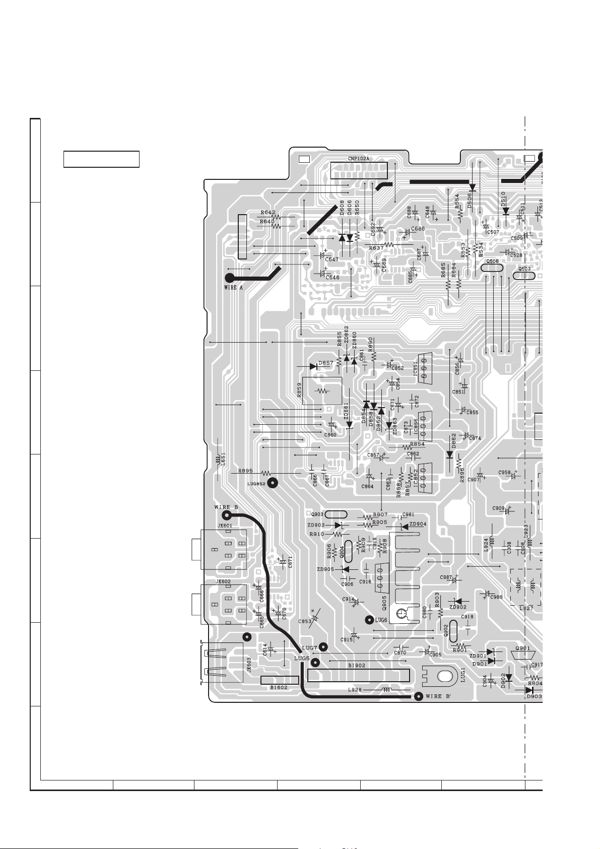
CD-SW440N
A
POWER PWB-B1
PRIMARY SECTION
3
B
4
C
1
D
2
1
2
3456 7
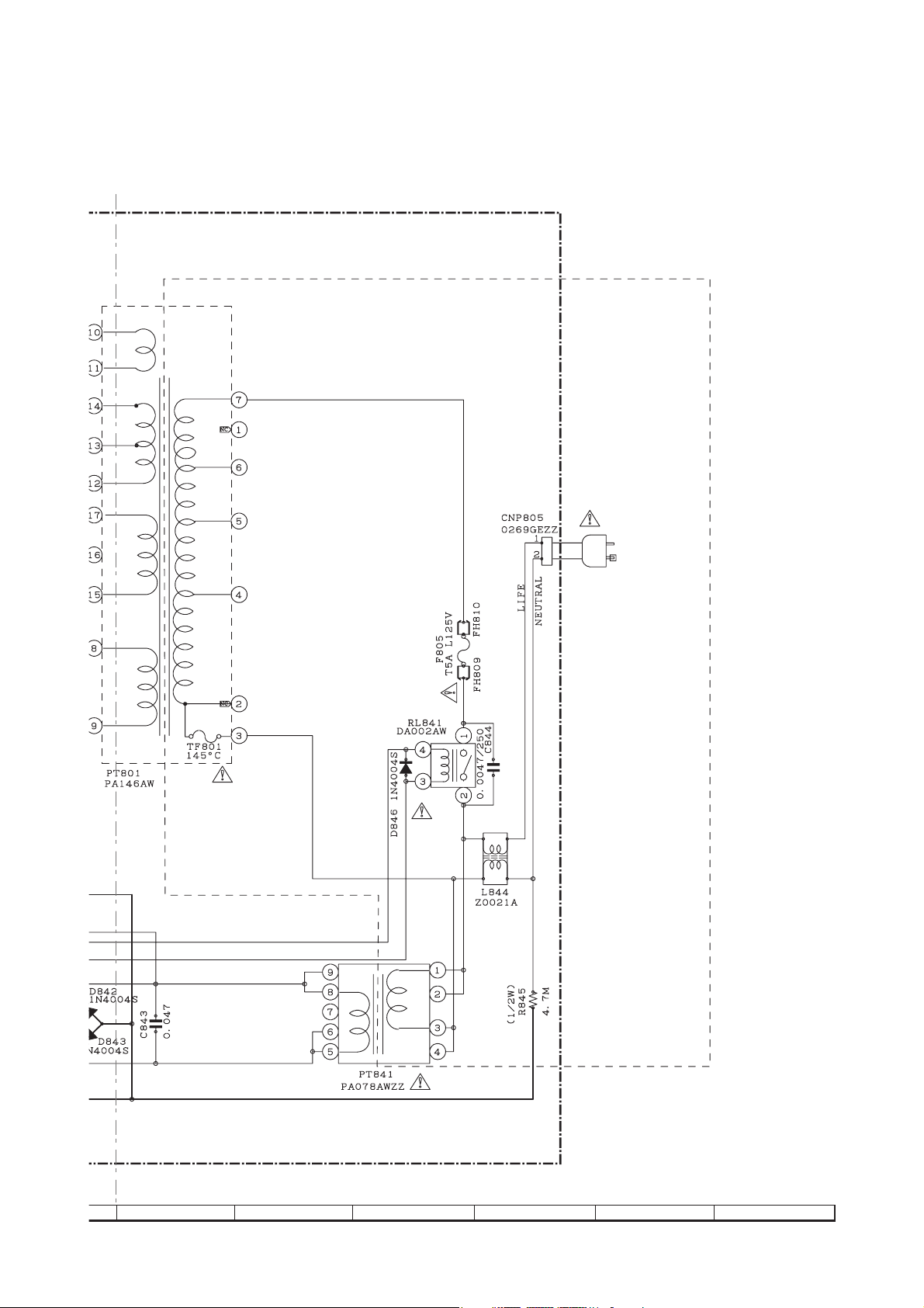
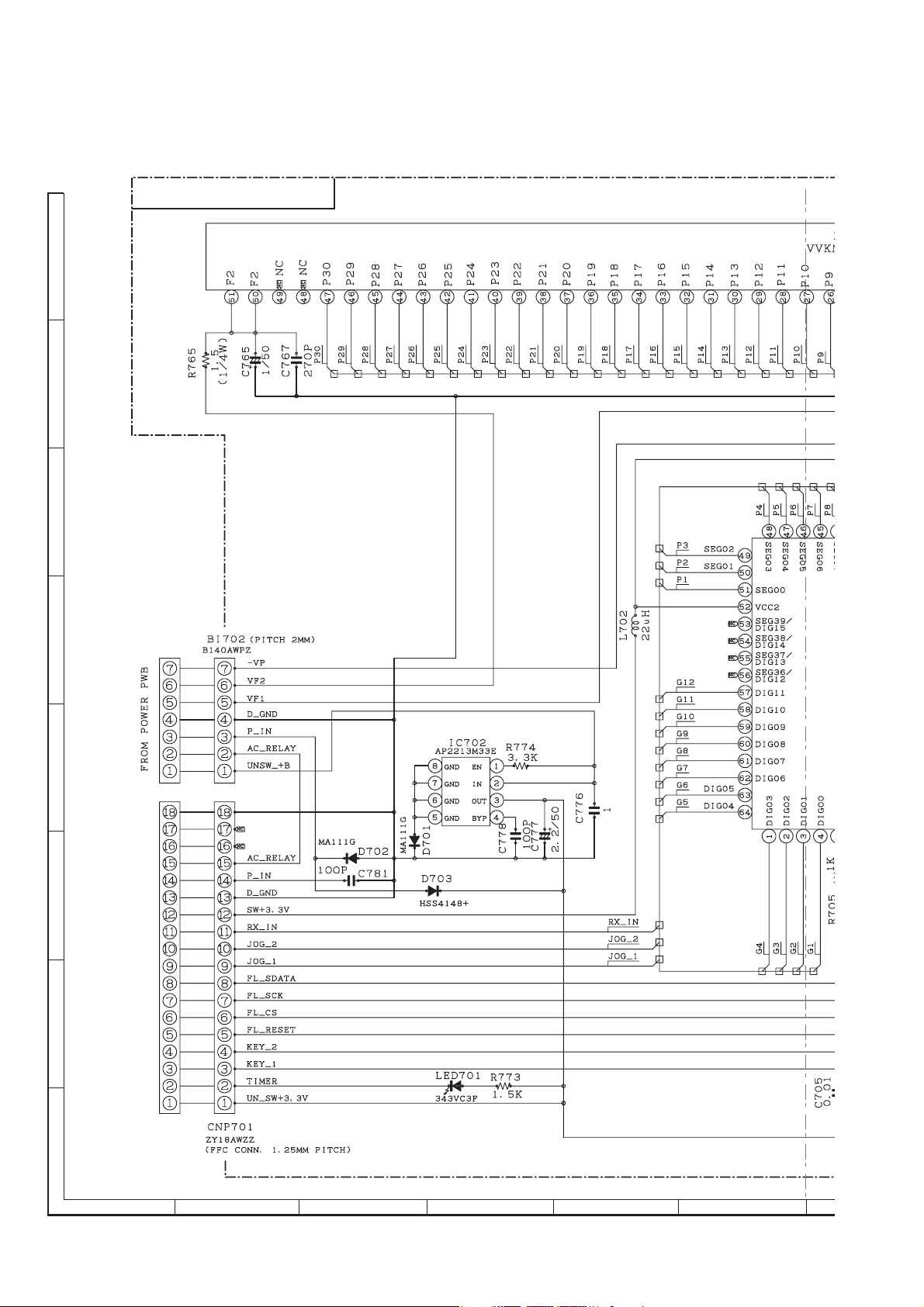
TF801
RL841
5A 125V
1.6A 125V
17 16 15 14 13 12 11 10 9 8
E
ECB
2A 125V
2A 125V
F
6A 125V
6A 125V
D802
ECB
123456789
1011 12
7 6 5 4 3 2 1
WH
SCREW
TO CHASSIS
(GND)
G
Lead-free solder indication
H
Lead-free solder is used in the POWER PWB.
Refer to "Precautions for handling lead-free solder" for instructions
and precautions.
COLOR TABLE
WH WHITE
1
23456
Figure 6-27: WIRING SIDE OF POWER PWB (TOP VIEW)
6 – 28
Page 45

-MEMO-
CD-SW440N
6 – 29
Page 46

CD-SW440N
A
DISPLAY/TAPE PWB-B2
B
C
54321
D
E
F
ECB
BCE
G
Lead-free solder indication
H
Lead-free solder is used in the DISPLAY/TAPE PWB.
Refer to "Precautions for handling lead-free solder" for instructions
and precautions.
1
23456
Figure 6-28: WIRING SIDE OF DISPLAY/TAPE PWB (TOP VIEW) (1/2)
ECB
12 3 4 5
ECB
ECB
6 – 30
Page 47

CD-SW440N
C
1234567
11131517
1012141618
ECB
7
8 9 10 11 12
Figure 6-29: WIRING SIDE OF DISPLAY/TAPE PWB (TOP VIEW) (2/2)
1
3579
2
468
6 – 31
Page 48

CD-SW440N
DISPLAY/TAPE PWB-B2
A
B
C
D
E
F
G
Lead-free solder indication
H
Lead-free solder is used in the DISPLAY/TAPE PWB.
Refer to "Precautions for handling lead-free solder" for instructions
and precautions.
1
23456
Figure 6-30: WIRING SIDE OF DISPLAY/TAPE PWB (BOTTOM VIEW) (1/2)
6 – 32
Page 49

CD-SW440N
7
8 9 10 11 12
Figure 6-31: WIRING SIDE OF DISPLAY/TAPE PWB (BOTTOM VIEW) (2/2)
6 – 33
Page 50

CD-SW440N
9
SERVO PWB-C
A
B
4321
11
1315171921232527293133
101214161820222426283032
C
D
EC B
E
E
E
C
4 6 8 10 12 14 16 182
1357 911131517
C
B
B
F
E
1234
CB
E
CB
1234 5 1234 56
G
H
1
23456
Figure 6-32: WIRING SIDE OF SERVO PWB (1/2)
6 – 34
Page 51

CD-SW440N
1
11
1315
1012146
3579
2468
123456
42
31
14 16
10 12
468
2
1234567 89
13 15
11
3379
1
E
E
C
C
B
B
AM
GND
ANTENNA
Lead-free solder indication
Lead-free solder is used in the SERVO PWB.
Refer to "Precautions for handling lead-free solder" for instructions
and precautions.
7
8 9 10 11 12
Figure 6-33: WIRING SIDE OF SERVO PWB (2/2)
6 – 35
FM
Page 52

CD-SW440N
iPod PWB-D
A
B
Q100
R140
C114
R136
R139
C
IC101
R138
R135
C113
R137
R122
R123
R134
R133
R128
R129
C111
C100
D
D107
CNP102
CNP101
E
JP101
JP102
R132
C104
R118
JP104
R110
R113
R107
R115
R121
C112
R131
R119
C108
C110
R120
C101
F
L101
D108
D109
C118
D105
D104
WIRE
BL
G
SCREW TO
CHASSIS (GND)
Lead-free solder indication
H
Lead-free solder is used in the iPod PWB.
Refer to "Precautions for handling lead-free solder" for instructions
and precautions.
1
23456
Figure 6-34: WIRING SIDE OF iPod PWB (TOP VIEW)
COLOR TABLE
BL BLUE
6 – 36
Page 53

A
B
C
CD-SW440N
iPod PWB-D
D
E
F
G
Lead-free solder indication
H
Lead-free solder is used in the iPod PWB.
Refer to "Precautions for handling lead-free solder" for instructions
and precautions.
1
23456
Figure 6-35: WIRING SIDE OF iPod PWB (BOTTOM VIEW)
6 – 37
Page 54

CD-SW440N
CHAPTER 7. FLOWCHART
[1] Troubleshooting
1. When the CD does not function
The CD section may not operate when the objectiv e lens of the optical pickup is dirty. Clean the objective lens, and
check the playback operation. When this section does not operate even after the above step is taken, check the
following items.
Remove the cabinet and follow the troubleshooting instructions.
"Track skipping and/or no TOC (Table Of Contents) may be caused by build up of dust other foreign matter on the
laser pickup lens. Before attempting any adjustment make certain that the lens is clean. If not, clean it as mentioned
below."
Turn the power off.
Gently clean the lens with a lens cleaning tissue and a small amount of isopropyl alcohol.
Do not touch the lens with the bare hand.
Parts code
1. CD optical pickup Lens cleaner disc UDSKA0004AFZZ
HOW TO USE
1.
Using the brush in the cleaner cap, apply 1 or 2 drops of the cleaning fluid to the
brush on the CD cleaner disc which has the mark next to it.
2.
Place the CD cleaner disc onto the CD disc tray with the brush side down, then
press the play button.
3.
You will hear music for about 20 seconds and the CD player will automatically stop.
If it still play continuously, press the stop button.
CAUTION
The CD lens cleaner should be effective for 30-50 operations, however if the
brushes become worn out earlier then please replace the cleaner disc.
If the CD cleaner brushes become very wet then wipe off any excess fluid with a soft
cloth.
Do not drink the cleaner fluid or allow it contact with the eyes. In the event of this
happening then drink and / or rinse with clean water and seek medical advice.
The CD cleaner disc must not be used on car CD players or on computer CD-ROM
drives.
All rights reserved. Unauthorized duplicating, broadcasting and renting this product
is prohibited by law.
2. When a CD cannot be played
Cleaning fluid
Cleaner disc
2.1. Pressing the CD operation key is accepted, but playback does not occur.
1) Focus system check
2) Tracking system check
3) Spin system check
4) Others
5) USB system check_USB play
7 – 1
Page 55

3. When the USB does not function.
1
2
FOO
TRO
4
3
1
TEI
RFO
FOO
3.1. “NO MEDIA” is displayed.
1) Check the power to U10 (92L117ALiM5601) and
CNP602 connector.
2) Check the system microcomputer (especially the
communication line with the USB Host).
3) Check the grounding condition to U10
(92L117ALiM5601) and CNP602 connector.
4. When a USB cannot be played.
4.1. Pressing the USB operation key is accepted,
but playback data does not occur.
1) DM data line.
2) DP data line.
3) Others.
CD-SW440N
Press the Tray1 CD Eject Button without inserting a disc, and try
starting the playback operation.
126
U10
127
U10
(1) Focus system check.
Figure 1
Although a CD is inserted and the cover is closed,
"NO DISC" is displayed.
1. Does the pickup move? No Sled motor.
Yes
2. Does the focus (lens) move up and down?
(Waveform drawing Figure 1)
Yes
3. Is the laser lit? No Check the laser diode driver Q5 peripheral circuit.
Yes
4. Is the turntable rotating? No Spindle motor.
When a disc is loaded, start playback operation.
1. Is focus servo activated?
(Waveform drawing Figure 2)
No Check the focus peripheral circuit.
No Pins 4, 7, 13 and 126 on U10, Pins 1, 13 and 14 on U12.
Check the laser diode driver Q5 peripheral circuit.
126
U10
13
U10
14
U10
Figure 2
7 – 2
Page 56

CD-SW440N
4
1
FOO
TEI
1
5
FOO
DMO
(2) Tracking system check.
Check the TE waveform at pin 14 on U10.
If the waveform shown in Figure 3 appears and soon after NO
DISC appears?
No
"Initialization" is possible, but play is not possible?
14
U10
126
U10
Yes
Yes
The tracking servo is not activated.
Check the peripheral circuits at pins 2, 3, 14 and 127 on U10,
pins 15, 16 and 26 on U12 and FFC.
A normal jump operation cannot be completed or the
beginning of the track cannot be found.
Check the around pin 127 on U10.
Figure 3
(3) Spin system check.
Press the OPEN/CLOSE switch without inserting a disc, and
then try starting the play operation.
1. The turntable rotates a little?
(Waveform drawing Figure 4)
No
2. The turntable doesn't rotate. Check around pin 123 on U10, pins 17, 18 and 23 on U12.
126
Yes
The spin driver circuit is OK.
U10
123
U10
Figure 4
7 – 3
Page 57

(4) Others.
DP
DM
9
The time is displayed normally, but no sound is produced. Or the sound has dropouts.
Is pin 33 and 36 on U10 (Figure 5), (Playback 1 kHz signal). No Check the audio out peripheral circuits.
Yes
If OK, Check the unit.
LINEOUTL
6
33
U10
7
36
U10
LINEOUTR
Figure 5
CD-SW440N
(5) USB system check_USB play.
Press USB function, insert the USB memory device into the
USB.
1. Does the device information can display? No Check around pin 52 and 53 on U10.
(Figure 6)
2. The waveform and the time is displayed normal, but no
sound is produced.
U10
52
53
No Check the audio out peripheral circuits.
U10
Figure 6
7 – 4
Page 58

CD-SW440N
CHAPTER 8. OTHERS
[1] Funtion Table Of IC
U6 92L117Si473101 : Broadcast AM/FM Radio Receiver ( 1/2 )
AMI
AM
ANT
RFGND
LNA
AGC
RDS
(Si4731)
LOW-IF
Si473x
DIGITAL
AUDIO
(Si4731)
DOUT
DFS
GPO/DCLK
FM
ANT
2.7-5.5 V
FMI
VDD
GND
LNA
AGC
LDO
ADC
DSP
ADC
AFC
RCLK
Figure 8-1 BLOCK DIAGRAM OF IC
CONTROL
INTERFACE
SEN
SCLK
DAC
DAC
SDIO
ROUT
LOUT
VIO
1.5-3.6 V
RST
NC
FMI
RFGND
AMI
RST
1
2
3
4
5
6
SEN
GPO2/INT
GPO1
NC
17181920
GND
PAD
10987
SDIO
SCLK
PIN CONFIGURATION
RCLK
8 – 1
DFS
GPO3/DCLK
16
DOUT
15
LOUT
14
ROUT
13
12
GND
11
VDD
VIO
Page 59

U6 92L117Si473101 : Broadcast AM/FM Radio Receiver ( 2/2 )
PIN DESCRIPTION
Pin Number(s) Name Description
1,20 NC No connect. Leave floating.
2 FMI FM RF inputs. FMI should be connected to the antenna trace.
3 RFGND RF ground. Connect to ground plane on PCB.
4 AMI AM RF input. AMI should be connected to the AM antenna.
5RST
6SEN
7 SCLK Serial clock input.
8 SDIO Serial data input/output.
9 RCLK External reference oscillator input.
10
11
12, GND PAD GND Ground. Connect to ground plane on PCB.
13 ROUT Right audio line output in analog output mode.
14 LOUT Left audio line output in analog output mode.
V
10
V
DD
Device reset (active low) input.
Serial enable input (active low).
I/O supply voltage.
Supply voltage. May be connected directly to battery.
CD-SW440N
15 DOUT Digital output data in digital output mode.
16 DFS Digital frame synchronization input in digital output mode.
17 GPO3/DCLK
18 GPO2/INT
19 GPO1 General purpose output.
General purpose output, crystal oscillator, or digital bit synchronous clock input in
digital output mode.
General purpose output or interrupt pin.
8 – 2
Page 60

CD-SW440N
U10 92L117ALiM5601 : CD,SD & USB Audio Single Chip Controller ( M5673 )( 1/6 )
Crystal
16.9344MHz
3.3V 1.8V
MIC in
FM in
Line in
I2S
SPDIF
I2C
master/slave
LCD
module
GPIO
SD/MMC
card
MS/MS pro
card
XTAL
PLL
Interface control logic
ADSP
CD
servo controller
& decoder
Motor
driver
Pickup
Head
Linear
regulator
ADC
DAC
CD ECC
& System
buffer
boost
Micro
Controller
Cache
Serial
Flash
MUX
MUX
L/R Line Out
USB host
Controller
USB
transceiver
USB
device
Figure 8-2 BLOCK DIAGRAM OF IC
8 – 3
Page 61

U10 92L117ALiM5601 : CD,SD & USB Audio Single Chip Controller ( M5673 )( 2/6 )
A
PIN DESCRIPTION
MDI
TRO
FOO
GPWM
AVSS33_1
DMO
AVDD33_1
FMO
VREF16
BTN_ADIN3
BTN_ADIN2
BTN_ADIN1
AVDD_D33
VDD_CORE
GND_CORE
VDD_PAD
GND_PAD
GPIOJ2
GPIOJ1
GPIOJ0/12CS_DAT
GPIO17/12S_CLK
GPIO16
GPIO15
GPIO14/PWM2
GPIO13/PWM1
GPIO12/IRC
CD-SW440N
LDO
TP1
TP2
MC
MB
MD
MA
AVDD33_2
HAVC
V12
AVSS33_2
TELP
MPXOUT1
MPXOUT2
MPXOUT3
COSP
COSN
AVDD33_3
VTB
VTP
AVSS33_3
AVSS33_LDO
AVDD33_LDO
AVDD18_LDO
VDD33_CKG
XTALI
XTALO
AVSS33_CKG
AVDD18_1
AVSS18_1
BCAPIL
BCAPOL
LINEOUTL
BCAPIR
BCAPOR
LINEOUTR
AVSS33_AUD
AVDD33_AUD
119
118
117
116
128
127
126
125
124
123
122
121
120
1
2
3
4
5
6
7
8
9
10
11
12
13
14
15
16
17
18
19
20
21
22
23
24
25
26
27
28
29
30
31
32
33
34
35
36
37
38
M5673
115
111
114
113
112
110
109
108
107
106
105
104
103
102
101
100
GPIO11/PWM0
GPIO10/LCDWRJ
GPIOH7/LCDRDJ
99
PRSTB
98
GPIOH6/LCDCSJ
97
GPIOH5/LCDA0
96
GPIOH4/DATA7
95
GPIOH3/DATA6
94
GPIOH2/DATA5
93
GPIOH1/DATA4
92
GPIOH0/DATA3
91
GPIOG7/DATA2
90
GPIOG6/DATA1
89
GPIOG5/DATA0
88
GPIOG4/USI_CLK
87
GPIOG3/USI_DI
86
GPIOG2/USI_DO
85
VDD_PAD
84
GND_PAD
83
GPIOF3/SD_MS_DET
82
GPIOF2/SD_MS_PWR
81
GPIOF1/SD_MS_CLK
80
GPIOF0/SDCMD/MSBS
79
GPIOE7/SDD3
78
GPIOE6/SDD2
77
GPIOE5/SDD1
76
GPIOE4/SDD0
75
GPIOE3/SD_MS_WP
74
GPIOE2/DOCD_CLK
73
GPIOE1/DOCD_DATI
72
GPIOE0/DOCD_DATO
71
GPIOD7/SPDIF
70
GPIOD6/12S_WCLK
69
GPIOD5/12S_DI
68
GPIOD4/12S_DO
67
GPIOD3/12S_REFCLK
66
GPIOD2/12S/SCLK
65
GPIOD1/12CM_DAT
39404142434445464748495051525354555657585960616263
DP
FMINR
LINEINR
MICIN
FMINL
LINEINL
V08L
MICBIAS
V15L
V08R
V15R
VREF
SFGP
SFGN
DM
GND_PAD
VDD_CORE
GND_CORE
VDD_PAD
GPIOB6/SFD0
GPIOB7/SFD1
GPIOC0/SFCSB
64
GPIOD0/12CM
GPIOC2/URTX
GPIOC3/URRX
GPIOC1/SFSCK
8 – 4
Page 62

CD-SW440N
U10 92L117ALiM5601 : CD,SD & USB Audio Single Chip Controller ( M5673 )( 3/6 )
PIN DESCRIPTION
PIN No. Signal Attribute Description
1 LDO O / A Laser Driver Output of APC
2 TP1 I / A 3 Beam Satellite PD Positive Input
3 TP2 I / A 3 Beam Satellite PD Negative Input
4 MC I / A Input of Main Beam Signal (C)
5 MB I / A Input of Main Beam Signal (B)
6 MD I / A Input of Main Beam Signal (D)
7 MA I / A Input of Main Beam Signal (A)
8 AVDD33_2 P Servo Analog Power
9 HAVC O / A Voltage Reference (programmable)
10 V12 O / A Voltage Reference (1.2V)
11 AVSS33_2 G Servo Analog Ground
12 TELP O / A Low Pass Filter Capacitor Connecting for TEZC Detection
13 MPXOUT1 O / A Multiplexer output 1 for Analog Signal Monitoring.
14 MPXOUT2 O / A Multiplexer output 2 for Analog Signal Monitoring.
15 MPXOUT3 O / A Multiplexer output 3 for Analog Signal Monitoring.
16 COSP O / A
17 COSN O / A
18 AVDD33_3 P PRML ADC Power
19 VTB B / O PRML ADC Voltage Control, connect to Capacitor
20 VTP B / O PRML ADC Voltage Control, connect to Capacitor
21 AVSS33_3 G PRML ADC Ground
22 AVSS33_LDO G LDO ground
23 AVDD33_LDO P LDO 3.3V input
24 AVDD18_LDO O / A LDO 1.8V output
25 AVDD33_CKG P Clock Generator Power
26 XTALI I / A External XTAL ( I ) , 16.9344MHz
27 XTALO O / A External XTAL ( O ) , 16.9344MHz
28 AVSS33_CKG G Clock Generator Ground
29 AVDD18_1 P Analog Power for PLL
30 AVSS18_1 G Analog Ground for PLL
31 BICAPL I / A Left Channel Bass capacitor in
External Capacitor Connection of Offset Cancellation Loop for VGA in
EQRF Block (Positive)
External Capacitor Connection of Offset Cancellation Loop for VGA in
EQRF Block (Negative)
32 BOCAPL O / A Left Channel Bass capacitor out
8 – 5
Page 63

U10 92L117ALiM5601 : CD,SD & USB Audio Single Chip Controller ( M5673 )( 4/6 )
PIN No. Signal Attribute Description
33 LINEOUTL O / A Left Channel Audio out
34 BICAPR I / A Right channel Bass capacitor in
35 BOCAPR O / A Right channel Bass capacitor out
36 LINEOUTR O / A Right Channel Audio out
37 AVSS33_AUD G VSS of ADC/DAC
38 AVDD33_AUD P VDD of ADC/DAC
39 FMINR I / A Right channel ADC FM in
40 LINEINR I / A Right channel ADC line in
41 MICIN I / A ADC MIC in
42 FMINL I / A Left channel ADC FM in
43 LINEINL I / A Left channel ADC line in
44 MICBIAS I / A MIC DC bias
45 V08L O / A Left channel VCM reference
46 V15L O / A Left channel voltage reference
47 V08R O / A Right channel VCM reference
48 V15R O / A Right channel voltage reference
CD-SW440N
49 VREF O / A Internal resistor string provide Vref
50 SFGP I / A DISC stop pos input/GPIO
51 SFGN I / A DISC stop neg input/GPIO
52 DM USB D53 DP USB D+
54 VDD_CORE P Digital Core power
55 GND_CORE G Digital Core ground
56 GND_PAD G Digital PAD Ground
57 VDD_PAD P Digital PAD power
58 GPIOB6/SFDO B / D GPIOB6/Seriel flash data input
59 GPIOB7/SFDI B / D GPIOB7/Seriel flash data output
60 GPIOC0/SFCSB B / D GPIOC0/Seriel flash csj
61 GPIOC1/SFSCK B / D GPIOC1/Seriel flash clk
62 GPIOC2/URTX B / D GPIOC2/RS-232 TX
63 GPIOC3/URRX B / D GPIOC3/RS-232 RX
64 GPIOD0/I2CM_CLK B / D GPIOD0/I2C clk output (M5673 is master)
65 GPIOD1/I2CM_DAT B / D GPIOD1/I2C data (M5673 is master)
66 GPIOD2/I2S_SCLK B / D GPIOD2/I2S bit clk output
67 GPIOD3/I2S_REFCLK B / D GPIOD3/I2S system(reference) clk output
68 GPIOD4/I2S_DO B / D GPIOD4/I2S data output
69 GPIOD5/I2S_DI B / D GPIOD5/I2S data input
70 GPIOD6/I2S_WCLK B / D GPIOD6/I2S word clk (LRCK) output
8 – 6
Page 64

CD-SW440N
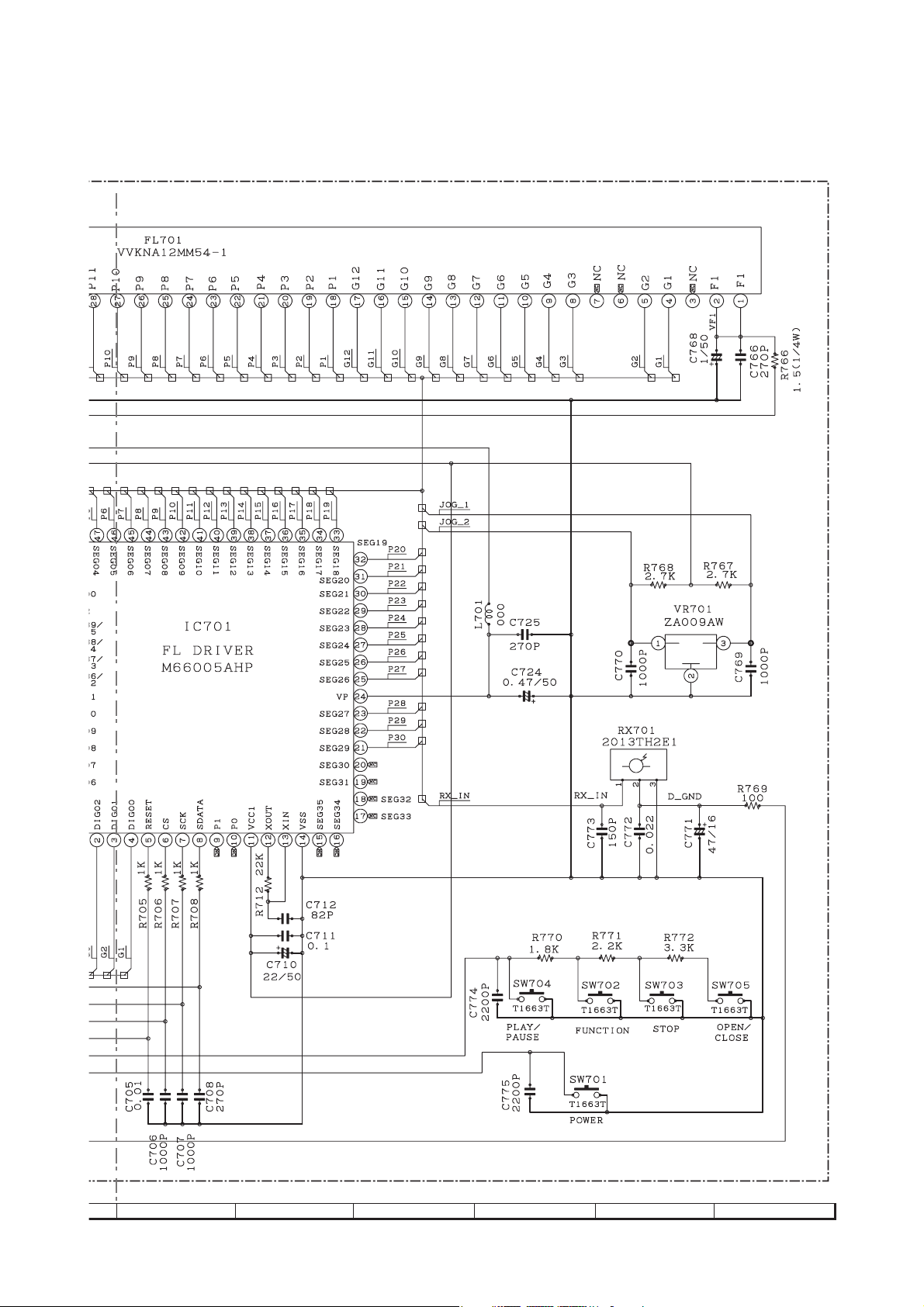
U10 92L117ALiM5601 : CD,SD & USB Audio Single Chip Controller ( M5673 )( 5/6 )
PIN No. Signal Attribute Description
71 GPIOD7/SPDIF B / D GPIOD7/SPDIF output
72 GPIOE0 B / D GPIOE0
73 GPIOE1 B / D GPIOE1
74 GPIOE2 B / D GPIOE2
75 GPIOE3 B / D GPIOE3
76 GPIOE4/SDD0 B / D GPIOE4/SD Card data0
77 GPIOE5/SDD1 B / D GPIOE5/SD Card data1
78 GPIOE6/SDD2 B / D GPIOE6/SD Card data2
79 GPIOE7/SDD3 B / D GPIOE7/SD Card data3
80 GPIOF0/SDCMD B / D GPIOF0/SD Card command
81 GPIOF1/SD_CLK B / D GPIOF/SD Card clk
82 GPIOF2 B / D GPIOF2
83 GPIOF3 B / D GPIOF3
84 GND_PAD G Digital PAD Ground
85 VDD_PAD P Digital PAD power
86 GPIOG2 B / D GPIOG2
87 GPIOG3 B / D GPIOG3
88 GPIOG4 B / D GPIOG4
89 GPIOG5/LCDDB0 B / D GPIOG5/LCD data0
90 GPIOG6/LCDDB1 B / D GPIOG6/LCD data1
91 GPIOG7/LCDDB2 B / D GPIOG7/LCD data2
92 GPIOH0/LCDDB3 B / D GPIOH0/LCD data3
93 GPIOH1/LCDDB4 B / D GPIOH1/LCD data4
94 GPIOH2/LCDDB5 B / D GPIOH2/LCD data5
95 GPIOH3/LCDDB6 B / D GPIOH3/LCD data6
96 GPIOH4/LCDDB7 B / D GPIOH4/LCD data7
97 GPIOH5/LCDRS B / D GPIOH5/LCD status/command
98 GPIOH6/LCDCSJ B / D GPIOH6/LCD CSJ
99 PRSTB B / D Chip reset, low active
100 GPIOH7/LCDRDJ B / D GPIOH7/LCD read control signal
101 GPIOI0/LCDWRJ B / D GPIOI0/LCD write control signal
102 GPIOI1/PWM0/LCD_ALE B / D GPIO/PWM0 output/LCD ALE signal when address/data share bus
103 GPIOI2/IRC B / D GPIOI2/ remote controller received
104 GPIOI3/PWM1 B / D GPIOI3/PWM1 output
105 GPIOI4/PWM2 B / D GPIOI4/PWM2 output
106 GPIOI5 B / D GPIOI5
107 GPIOI6 B / D GPIOI6
8 – 7
Page 65

U10 92L117ALiM5601 : CD,SD & USB Audio Single Chip Controller ( M5673 )( 6/6 )
PIN No. Signal Attribute Description
108 GPIOI7/I2CS_CLK B / D GPIOI7/I2C clk M5673 is slave
109 GPIOJ0/I2CS_DAT B / D GPIOJ0/I2C data when M5673 is slave
110 GPIOJ1 B / D GPIOJ1
111 GPIOJ2 B / D GPIOJ2
112 GND_PAD G Digital PAD Ground
113 VDD_PAD P Digital PAD power
114 GND_CORE G Digital Core ground
115 VDD_CORE P Digital Core power
116 AVDD_D33 P 3.3V for digital circuit in analog.
117 BTN_ADIN1 I / A Bottom check input, connect to servo ADC
118 BTN_ADIN2 I / A Bottom check input, connect to servo ADC
119 BTN_ADIN3 I / A Bottom check input, connect to servo ADC
120 VREF16 O / A SERVO DAC common mode voltage
121 FMO O / A Focus servo output. 3 level PWM output.
122 AVDD33_1 P Servo Analog Power
123 DMO O / A Disk motor control output. 3 level PWM output.
CD-SW440N
124 AVSS33_1 G Servo Anolog Ground
125 GPWM O / A General purpose 3 level PWM output
126 FOO O / A Focus servo output. 3 level PWM output.
127 TRO O / A Tracking servo output. 3 level PWM output.
128 MDI I / A Laser Power Monitor Input For APC
The definitions of the signal attributes:
D: Digital
I: Input
O: Output
B: Bi-direction
P: Power
G: Ground
A: Analog Pad
8 – 8
Page 66

CD-SW440N
TOTAL
MEMORY
SLEEP
5
TITLE-3
TITLE-2
TITLE-1
FOLD
PTYI
WMA
ST
REC
TA
TP
DAILY
MHz
MP3
RDS
kHz
4
3
2
1
X-BASS
)
(
MP3
WMA
TOTAL
[2] FL Display
FL701 VVKNA12MM54-1
GRID ASSIGNMENT
ANODE CONNECTION
1G
P1
P2
P3
P4
P5
D5a
P6
D5b
P7
D5c
P8
P9
D4a
P10
D4b
P11
D4c
P12
P13
D3a
P14
D3b
P15
D3c
P16
P17
D2a
P18
D2b
P19
D2c
P20
P21
D1a
P22
D1b
P23
D1c
P24
P25
P26
P27
P28
P29
P30
OUTER DIMENSIONS
h
r
Dot1
a
j
p
n
d
col2
Dot2
2a
col1
k
12G
2a
11G8G
b
m
c
1a
1b
1k
1j
1h
1f
1m
1d
1g
1p
1e
1n
1r
1c
2a
2b
2k
2j
2h
2f
2m
2d
2g
2p
2e
2n
2r
2c
1G
1a 1a 1a 1a 1a 1a 1a 1a 1a 1a
2a 2a 2a 2a 2a 2a 2a
2G 3G 4G 5G 6G 7G 9G 10G
D5b
D4b
D3b
D2b
D1b
D3a
1a
1b
1k
1j
1h
1f
1m
1d
1g
1p
1e
1n
1r
1c
2a
2b
2k
2j
2h
2f
2m
2d
2g
2p
2e
2n
2r
2c
D5a
D4a
D2a
D1a
D5c
D4c
D3c
D2c
D1c
1a
1b
1k
1j
1h
1f
1m
1d
1g
1p
1e
1n
1r
1c
2a
2b
2k
2j
2h
2f
2m
2d
2g
2p
2e
2n
2r
2c
1a
1b
1k
1h
1m
1d
1g
1p
1e
1n
1c
2a
2b
2k
2h
2m
2d
2g
2p
2e
2n
2c
f
g
e
(2G~11G)
1a
1b
1j
1f
1r
2j
2f
2r
1k
1j
1h
1f
1m
1d
1g
1p
1e
1n
1r
1c
2a
2b
2k
2j
2h
2f
2m
2d
2g
2p
2e
2n
2r
2c
1
D5a
D4a
D3a
(1G)
D2a
D1a
2G 3G 4G 5G 6G 7G 8G 9G
1a
1b
1k
1j
1h
1f
1m
1d
1g
1p
1e
1n
1r
1c
2a
2b
2k
2j
2h
2f
2m
2d
2g
2p
2e
2n
2r
2c
1a
1b
1k
1j
1h
1f
1m
1d
1g
1p
1e
1n
1r
1c
2a
2b
2k
2j
2h
2f
2m
2d
2g
2p
2e
2n
2r
2c
51
2a
1a
1b
1k
1j
1h
1f
1m
1d
1g
1p
1e
1n
1r
1c
2a
2b
2k
2j
2h
2f
2m
2d
2g
2p
2e
2n
2r
2c
Dot1
Dot2
10G
1a
1b
1k
1j
1h
1f
1m
1d
1g
1p
1e
1n
1r
1c
2a
2b
2k
2j
2h
2f
2m
2d
2g
2p
2e
2n
2r
2c
Col1
Col2
11G 12G
1a
1b
1k
1j
1h
1f
1m
1d
1g
1p
1e
1n
1r
1c
2a
2b
2k
2j
2h
2f
2m
2d
2g ( )
2p
2e
2n
2r
2c
(L)
(R)
PIN CONNECTION
PIN NO.
CONNECTION
PIN NO.
CONNECTION
PATTERN AREA
45
44 43 42 415051 49 48 47 46 40 39 38 37 36 35 34 33 32 31 30 29 28 27 26
F2 F2 NP NP P29P30 P28 P27 P25P26 P24 P23 P22 P21 P20 P19 P18 P17 P16 P15 P14 P12P13 P11 P10 P9
20
25 24 23 22 21
P8 P7 P6 P5 P4
19 18 17 16 15 14 13 12 11 10 9 8 7 6 5 4 3 2 1
P3 P2 P1 12G 11G 10G 9G 8G 7G 6G 5G 4G 3G NX NX 2G 1G NP F1 F1
8 – 9
Page 67

PARTS GUIDE
MINI COMPONENT SYSTEM
CD-SW440N
[1] INTEGRATED CIRCUITS
[2] TRANSISTORS
[3] DIODES
[4] TRANSFORMERS
[5] COILS
[6] CRYSTALS / VIBRATORS
[7] CAPACITORS
[8] RESISTORS
Explanation of capacitors/resistors parts codes
MODEL
CD-SW440N Mini Component System consisting of
CD-SW440N (main unit), CP-S440N (speaker system) and
CP-SW440N (subwoofer).
CONTENTS
[9] OTHER CIRCUITRY PARTS
[10] CABINET PARTS /
CD MECHANISM PARTS
[11] FRONT SPEAKER BOX PARTS
[12] SUBWOOFER BOX PARTS
[13] ACCESSORIES / PACKING PARTS
[14] P.W.B. ASSEMBLY
[15] OTHER SERVICE PARTS
CD-SW440N
Capacitors
VCC ....................... Ceramic type
VCK ........................ Ceramic type
VCT ........................ Semiconductor type
VC • • MF ............... Cylindrical type (without lead wire)
VC • • MN ............... Cylindrical type (without lead wire)
VC • • TV ................ Square type (without lead wire)
VC • • TQ ............... Square type (without lead wire)
VC • • CY ............... Square type (without lead wire)
VC • • CZ ............... Square type (without lead wire)
VC•••••••••J..The13thcharacter represents capacity difference.
("J" ±5%, "K" ±10%, "M" ±20%, "N" ±30%,
"C" ±0.25 pF, "D" ±0.5 pF, "Z" +80-20%.)
If there are no indications for the electrolytic capacitors, error is ±20%.
Resistors
VRD ....................... Carbon-film type
VRS ........................ Carbon-film type
VRN ....................... Metal-film type
VR • • MF ............... Cylindrical type (without lead wire)
VR • • MN ............... Cylindrical type (without lead wire)
VR • • TV ................ Square type (without lead wire)
VR • • TQ ............... Square type (without lead wire)
VR • • CY ............... Square type (without lead wire)
VR • • CZ ............... Square type (without lead wire)
VR•••••••••J..The13th character represents error.
("J" ±5%, "F" ±1%, "D" ±0.5%.)
If there are no indications for other parts, the resistors are ±5%
carbon-film type.
Explanation of PWB Assembly parts code category
S Category -- Repair ( Component parts of PWB can be replace and repair, PWB no supply )
X Category -- Replacement ( PWB can not be repair. Component parts no supply )
S.X Category -- Repair and Replacement ( PWB can repair and replace )
KG Category -- Revolve repair by Business Center ( Return to Business Center and repair by manufacturer. Component parts no supply )
Parts marked with " " are important for maintaining the safety of the set. Be sure to replace these parts with specified
ones for maintaining the safety and performance of the set.
!
SHARP CORPORATION
This document has been published to be used
for after sales service only.
The contents are subject to change without notice.
Page 68

CD-SW440N
NO. PARTS CODE
PRICE
RANK
[1] INTEGRATED CIRCUITS
iC101 VHI341S2161-1 AQ Apple Authentication Class 3 IC
iC301 VHITDA8920CJ1 AY D-Class Power IC, TDA8920
iC401 VHIAN7345K/-1 AM Pre Amp, AN7345
iC503 VHIAZ4558CME1 AD Pre Amplifier, AZ4558
iC603 VHIBH3547F+-1 AE Headphone Amplifier
iC604 VHIAZ4558CME1 AD Pre Amplifier, AZ4558
iC701 VHIM66005AHP1 AS FL Driver
iC702 VHIAP2213M33E AE Voltage Regulator, 3.3V
iC851 VHIAN80T53/-1 AL Multi Regulator, AN80T53
iC852 VHIKIA7805AP1 AF Constant Voltage Regulator, KIA7805AP
iC853 VHIAP2213M33E AE Voltage Regulator, 3.3V
iC855 VHITPS2052BD1 AH Dual Channel Current
iC901 VHITDA8920CJ1 AY D-Class Power IC, TDA8920
iC902 VHI74HCU04P-1 AD Inverter IC, 74HCU04
U1 92L117R5F21201 R5F212A8, 64 Pin
U2 92L1170024C021 S524A40X21
U3 92L117NJU73911 N JU7391V
U6 92L117Si473001 Si4730, 20 Pin
U8 92L11700045582 AC 4558
U10 92L117ALiM5601 ALiM5673, 128 Pin
U11 92L117EON2M001 EON 2M FLASH
U12 92L1170AM58881 AF AM5888, 28 Pin
[2] TRANSISTORS
Q1 92L11300080501 8050
Q2 92L11300085501 8550
Q3 92L113KRC104S1 KRC104 S
Q4 92L113KRC104S1 KRC104 S
Q5 92L1132SB11323 2SB1132
Q6 92L11300085501 8550
Q7 92L11300080501 8050
Q8 92L1132SB77201 2SB772,PNP,3A/30V
Q9 92L11300039042 AB 3904
Q11 92L113KRC104S1 KRC104 S
Q13 92L113KRC104S1 KRC104 S
Q100 VSKRA107S//-1 AB Digital,PNP,KRA107 S
Q324 VSKRC104S//-1 AC Digital,NPN,KRC104 S
Q325 VSKRC104S//-1 AC Digital,NPN,KRC104 S
Q405 VSKTC3875GR-1 AB Silicon,NPN,KTC3875 GR
Q406 VSKTC3875GR-1 AB Silicon,NPN,KTC3875 GR
Q502 VSKTC3875GR-1 AB Silicon,NPN,KTC3875 GR
Q503 VSKTC3205Y/-1 AD Silicon,NPN,KTC3205 Y
Q504 VSKTC3875GR-1 AB Silicon,NPN,KTC3875 GR
Q506 VSKTC3203Y/-1 AC Silicon,NPN,KTC3203 Y
Q507 VSKRC104S//-1 AC Digital,NPN,KRC104 S
Q601 VSKRA102S//-1 AB Digital,PNP,KRA102 S
Q602 VSKTC3875GR-1 AB Silicon,NPN,KTC3875 GR
Q603 VSKTC3875GR-1 AB Silicon,NPN,KTC3875 GR
Q604 VSKTC3875GR-1 AB Silicon,NPN,KTC3875 GR
Q605 VSKTC3875GR-1 AB Silicon,NPN,KTC3875 GR
Q606 VSKTA1504GR-1 AB Silicon,PNP,KTA1504 GR
Q607 VSKTC3875GR-1 AB Silicon,NPN,KTC3875 GR
Q608 VSKTC3875GR-1 AB Silicon,NPN,KTC3875 GR
Q709 92L11300085501 8550
Q711 92L11300085501 8550
Q801 VSKTA1274Y/-1 AE Silicon,PNP,KTA1274 Y
Q841 VSKTC3199GR-1 AB Silicon,NPN,KTC3199 GR
Q851 VSKRC104S//-1 AC Digital,NPN,KRC104 S
Q852 VSKTA1504GR-1 AB Silicon,PNP,KTA1504 GR
Q853 VSKRC104S//-1 AC Digital,NPN,KRC104 S
Q902 VSKTC3203Y/-1 AC Silicon,NPN,KTC3203 Y
Q903 VSKTA1266GR-1 AB Silicon,PNP,KTA1266 GR
Q904 VSKTC3203Y/-1 AC Silicon,NPN,KTC3203 Y
Q906 VSKTC3203Y/-1 AC Silicon,NPN,KTC3203 Y
Q922 VSKRC107S//-1 AB Digital,NPN,KRC107 S
Q923 VSKRC107S//-1 AB Digital,NPN,KRC107 S
Q924 VSKRC104S//-1 AC Digital,NPN,KRC104 S
Q925 VSKRC104S//-1 AC Digital,NPN,KRC104 S
Q926 VSKTC3875GR-1 AB Silicon,NPN,KTC3875 GR
Q927 VSKTA1504GR-1 AB Silicon,PNP,KTA1504 GR
Q928 VSKRA107S//-1 AB Digital,PNP,KRA107 S
Q929 VSKRC104S//-1 AC Digital,NPN,KRC104 S
[3] DIODES
D1 92L10901N41482 AB 1N4148
D2 92L10901N41482 AB 1N4148
D3 92L10901N41482 AB 1N4148
D4 92L10901N41482 AB 1N4148
D5 92L10901N41482 AB 1N4148
D6 92L10901N41482 AB 1N4148
D7 92L10901N41482 AB 1N4148
D8 92L10901N41482 AB 1N4148
D10 92L10901N41482 AB 1N4148
D11 92L10901N41482 AB 1N4148
D12 92L10901N41482 AB 1N4148
D13 92L10901N41482 AB 1N4148
D14 92L10901N41482 AB 1N4148
NEW
MARK
PART
RANK
DESCRIPTION
1
Page 69

NO. PARTS CODE
PRICE
RANK
NEW
MARK
[3] DIODES
D15 92L10901N41482 AB 1N4148
D104 VHDMA111G++-1 AB Silicon,MA111
D105 VHDMA111G++-1 AB Silicon,MA111
D108 VHDMA111G++-1 AB Silicon,MA111
D109 VHDMA111G++-1 AB Silicon,MA111
D312 VHDHSS4148+-1 AA Silicon,HSS4148
D313 VHDHSS4148+-1 AA Silicon,HSS4148
D320 VHDMA111G++-1 AB Silicon,MA111
D321 VHDMA111G++-1 AB Silicon,MA111
D322 VHDMA111G++-1 AB Silicon,MA111
D323 VHDMA111G++-1 AB Silicon,MA111
D328 VHD1N4004S/-1 AB Silicon,1N4004S
D329 VHD1N4004S/-1 AB Silicon,1N4004S
D330 VHDMA111G++-1 AB Silicon,MA111
D501 VHDMA111G++-1 AB Silicon,MA111
D503 VHDMA111G++-1 AB Silicon,MA111
D504 VHDMA111G++-1 AB Silicon,MA111
D506 VHDHSS4148+-1 AA Silicon,HSS4148
D508 VHDMA111G++-1 AB Silicon,MA111
D510 VHDHSS4148+-1 AA Silicon,HSS4148
D601 VHDMA111G++-1 AB Silicon,MA111
D602 VHDMA111G++-1 AB Silicon,MA111
D606 VHDHSS4148+-1 AA Silicon,HSS4148
D607 VHDMA111G++-1 AB Silicon,MA111
D608 VHDHSS4148+-1 AA Silicon,HSS4148
D609 VHDMA111G++-1 AB Silicon,MA111
D611 VHDMA111G++-1 AB Silicon,MA111
D612 VHDMA111G++-1 AB Silicon,MA111
D701 VHDMA111G++-1 AB Silicon,MA111
D702 VHDMA111G++-1 AB Silicon,MA111
D703 VHDHSS4148+-1 AA Silicon,HSS4148
D802 VHDD10XB60F-1 AL Rectifier, D10XB60
D803 VHDGDRL204+-1 AC Silicon,RL204
D804 VHDGDRL204+-1 AC Silicon,RL204
D805 VHD1N4004S/-1 AB Silicon,1N4004S
D806 VHD1N4004S/-1 AB Silicon,1N4004S
D812 VHD1N4004S/-1 AB Silicon,1N4004S
D813 VHD1N4004S/-1 AB Silicon,1N4004S
D814 VHD1N4004S/-1 AB Silicon,1N4004S
D815 VHD1N4004S/-1 AB Silicon,1N4004S
D842 VHD1N4004S/-1 AB Silicon,1N4004S
D843 VHD1N4004S/-1 AB Silicon,1N4004S
D844 VHD1N4004S/-1 AB Silicon,1N4004S
D845 VHD1N4004S/-1 AB Silicon,1N4004S
D846 VHD1N4004S/-1 AB Silicon,1N4004S
D851 VHDMA111G++-1 AB Silicon,MA111
D852 VHDHSS4148+-1 AA Silicon,HSS4148
D853 VHD1N4004S/-1 AB Silicon,1N4004S
D854 VHDHSS4148+-1 AA Silicon,HSS4148
D855 VHDMA111G++-1 AB Silicon,MA111
D856 VHDMA111G++-1 AB
7 VHDHSS4148+-1 AA Silicon,HSS4148
D85
D859 VHDMA111G++-1 AB Silicon,MA111
D860 VHDMA111G++-1 AB Silicon,MA111
D901 VHDGD1A4+++-1 AB Silicon,GD1A4
D902 VHDGD1A4+++-1 AB Silicon,GD1A4
D903 VHDGD1A4+++-1 AB Silicon,GD1A4
D912 VHDMA111G++-1 AB Silicon,MA111
D913 VHDHSS4148+-1 AA Silicon,HSS4148
D920 VHDMA111G++-1 AB Silicon,MA111
D921 VHDMA111G++-1 AB Silicon,MA111
D922 VHDMA111G++-1 AB Silicon,MA111
D923 VHDMA111G++-1 AB Silicon,MA111
D928 VHD1N4004S/-1 AB Silicon,1N4004S
D929 VHD1N4004S/-1 AB Silicon,1N4004S
D930 VHDMA111G++-1 AB Silicon,MA111
LED504 VHPSDPB40F2AC AH LED,Blue
LED701 VHPSLR343VC3F AC LED,Red
LED702 VHPSDPB40F2AC AH LED,Blue
ZD1 92L11000910052 AB Zener, 9.1V
ZD2 92L11000560051 Zener, 5.6V
ZD3 92L11000560051 Zener, 5.6V
ZD801 VHEZJ6R2A++1E AB Zener, 6.2V
ZD802 VHEZJ6R2A++1E AB Zener, 6.2V
ZD803 VHEZJ30B+++1E AB Zener, 30V
ZD860 VHEZJ6R8B++1E AB Zener, 6.8V
ZD861 VHEZJ6R8B++1E AB Zener, 6.8V
ZD862 VHEZJ15B+++1E AB Zener, 15V
ZD901 VHEZJ10B+++1E AB Zener, 10V
ZD902 VHEZJ30B+++1E AB Zener, 30V
ZD903 VHEZJ6R2A++1E AB Zener, 6.2V
ZD904 VHEZJ24B+++1E AB Zener, 24V
ZD905 VHEZJ10B+++1E AB Zener, 10V
ZD906 RH-EXA523WJZZ AB Zener, 5.6V
[4] TRANSFORMERS
!
!
PT801 RTRNPA146AWZZ Power ( Main )
PT841 RTRNPA078AWZZ AM Power ( Sub )
PART
RANK
CD-SW440N
DESCRIPTION
Silicon,MA111
2
Page 70

CD-SW440N
NO. PARTS CODE
[5] COILS
FB7 92L10606030008 AA Impedence, 300
FB10 92L10606030008 AA Impedence, 300
FB11 92L10606030008 AA Impedence, 300
FB12 92L10606030008 AA Impedence, 300
FB13 92L10606030008 AA Impedence, 300
FB14 92L10606030008 AA Impedence, 300
FB15 92L10606030008 AA Impedence, 300
FB16 92L10606030008 AA Impedence, 300
FB17 92L10606030008 AA Impedence, 300
FB18 92L10606030008 AA Impedence, 300
FB19 92L10606030008 AA Impedence, 300
FB20 92L10606030008 AA Impedence, 300
FB21 92L10606030008 AA Impedence, 300
FB22 92L10606030008 AA Impedence, 300
FB23 92L10606030008 AA Impedence, 300
FB24 92L10606030008 AA Impedence, 300
FB25 92L10606030008 AA Impedence, 300
FB26 92L10606030008 AA Impedence, 300
FB27 92L10606030008 AA Impedence, 300
FB28 92L10606030008 AA Impedence, 300
FB29 92L10606030008 AA Impedence, 300
FB30 92L10606030008 AA Impedence, 300
FB31 92L10606030008 AA Impedence, 300
FB32 92L10606030008 AA Impedence, 300
FB33 92L10606030008 AA Impedence, 300
FB44 92L10606030008 AA Impedence, 300
FB45 92L10606030008 AA Impedence, 300
FB46 92L10606030008 AA Impedence, 300
FB47 92L10606030008 AA Impedence, 300
FB48 92L10606030008 AA Impedence, 300
FB49 92L10606030008 AA Impedence, 300
FB50 92L10606030008 AA Impedence, 300
FB52 92L10606030008 AA Impedence, 300
FB53 92L10606030008 AA Impedence, 300
FB54 92L10606030008 AA Impedence, 300
FB55 92L10606030008 AA Impedence, 300
FB56 92L10606030008 AA Impedence, 300
FB57 92L10606030008 AA Impedence, 300
FB59 92L10606030008 AA Impedence, 300
FB60 92L10606030008 AA Impedence, 300
FB61 92L10606030008 AA Impedence, 300
FB63 92L10606030008 AA Impedence, 300
FB64 92L10606030008 AA Impedence, 300
FB65 92L10606030008 AA Impedence, 300
FB66 92L10606030008 AA Impedence, 300
FB67 92L10606030008 AA Impedence, 300
FB68 92L10606030008 AA Impedence, 300
FB69 92L10606030008 AA Impedence, 300
FB70 92L10606030008 AA Impedence, 300
FB71 92L10606030008 AA Impedence, 300
FB72 92L10606030008 AA
B73 92L10606030008 AA Impedence, 300
F
FB74 92L10606030008 AA Impedence, 300
FB75 92L10606030008 AA Impedence, 300
FB76 92L10606030008 AA Impedence, 300
FB77 92L10606030008 AA Impedence, 300
FB78 92L10606030008 AA Impedence, 300
FB79 92L10606030008 AA Impedence, 300
FB88 92L10606030008 AA Impedence, 300
FB90 92L10606030008 AA Impedence, 300
FB91 92L10606030008 AA Impedence, 300
FB93 92L10606030008 AA Impedence, 300
FB95 92L10606030008 AA Impedence, 300
FB96 92L10606030008 AA Impedence, 300
FB611 RBLN-0061TAZZ AB Chip Ferrite Core
FB612 RBLN-0061TAZZ AB Chip Ferrite Core
FB613 RBLN-0061TAZZ AB Chip Ferrite Core
L1 92L10606030011 Impedence, 80, 100MHz
L2 92L10606030011 Impedence, 80, 100MHz
L3 92L10606030011 Impedence, 80, 100MHz
L4 92L10606030011 Impedence, 80, 100MHz
L5 92L10606030011 Impedence, 80, 100MHz
L6 92L10606030011 Impedence, 80, 100MHz
L7 92L10606030011 Impedence, 80, 100MHz
L8 92L10606030011 Impedence, 80, 100MHz
L9 92L10606030011 Impedence, 80, 100MHz
L10 92L10606030011 Impe dence, 80, 100MHz
L11 92L10606030011 Impe dence, 80, 100MHz
L12 92L10606030011 Impe dence, 80, 100MHz
L13 92L10606030011 Impe dence, 80, 100MHz
L18 92L10606030011 Impe dence, 80, 100MHz
L30 92L10606030011 Impe dence, 80, 100MHz
L320 RCILZ0055AWZZ AH Coil
L323 RCILZ2130SCT5 AC Coil
L324 RCILZ2130SCT5 AC Coil
L325 RCILZ0024AWZZ AF 22 mH, Peaking
L702 VP-DH220K0000 AB 22 µ H, Peaking
!
L844 RCILZ0021AWZZ AF AC Line Filter
L920 RCILZ0055AWZZ AH Coil
PRICE
RANK
NEW
MARK
PART
RANK
DESCRIPTION
Impedence, 300
3
Page 71

NO. PARTS CODE
PRICE
RANK
NEW
MARK
PART
RANK
[5] COILS
L921 RCILZ0055AWZZ AH Coil
L923 RCILZ2130SCT5 AC Coil
L924 RCILZ2130SCT5 AC Coil
L925 RCILZ0024AWZZ AF 22 mH, Peaking
L927 RCILZ0049AWZZ AH Coil
L928 RCORF0015AWZZ AB Core
T1 92L108SL755TF1 AM C o il
[6] CRYSTALS / VIBRATORS
X901 RCRM-A019AWZZ AD Resonator 830K
X902 RCRM-A018AWZZ AD Resonator 750K
Y1 92L12780000202 Crystal, 8 MHz
Y2 92L12732768203 Crystal, 32.768 KHz
Y3 92L12732768203 Crystal, 32.768 KHz
Y4 92L12716920102 Crystal, 16.9344 MHz
[7] CAPACITORS
BC1 92L104104Z0601 AA 0.1 µF,50V
BC2 92L104104Z0601 AA 0.1 µF,50V
BC3 92L104104Z0601 AA 0.1 µF,50V
BC4 92L104104Z0601 AA 0.1 µF,50V
BC5 92L104104Z0601 AA 0.1 µF,50V
BC6 92L104104Z0601 AA 0.1 µF,50V
BC7 92L104104Z0601 AA 0.1 µF,50V
C1 92L104104Z0601 AA 0.1 µF,50V
C2 92L104104Z0601 AA 0.1 µF,50V
C3 92L104104Z0601 AA 0.1 µF,50V
C4 92L104104Z0601 AA 0.1 µF,50V
C5 92L104104Z0601 AA 0.1 µF,50V
C6 92L104104Z0601 AA 0.1 µF,50V
C7 92L104220J0601 22 pF ,50V
C8 92L104220J0601 22 pF ,50V
C9 92L104220J0601 22 pF ,50V
C10 92L104220J0601 22 pF,50V
C11 92L104104Z0601 AA 0.1 µF,50V
C12 92L104105M0606 1 µF,50V,Electrolytic
C13 92L104272K0601 2 700 pF,50V
C14 92L104105M0606 1 µF,50V,Electrolytic
C15 92L104106M0407 10 µF,25V,Electrolytic
C16 92L104105M0606 1 µF,50V,Electrolytic
C17 92L104475M0202 AB 4.7 µF,10V
C18 92L104154K0601 0.15 µF,50V
C19 92L104184K0601 0.18 µF,50V
C20 92L104105M0606 1 µF,50V,Electrolytic
C21 92L104105M0601 AA 1 µF,50V
C22 92L104472K0601 4 700 pF,50V
C23 92L104105M0606 1 µF,50V,Electrolytic
C24 92L104104Z0601 AA 0.1 µF,50V
C25 92L104105M0606 1 µF,50V,Electrolytic
C26 92L104105M0601 AA 1 µF,50V
C27 92L104105M0606 1 µF,50V,Electrolytic
C28 92L104472K0601 4 700 pF,50V
C29 92L104105M0606 1 µF,50V,Electrolytic
C30 92L104154K0601 0.15 µF,50V
C31 92L104184K0601 0.18 µF,50V
C32 92L104475M0202 AB 4.7 µF,10V
C33 92L104105M0606 1 µF,50V,Electrolytic
C34 92L104106M0407 10 µF,25V,Electrolytic
C35 92L104330J0601 33 pF,50V
C36 92L104330J0601 33 pF,50V
C37 92L104105M0606 1 µF,50V,Electrolytic
C38 92L104272K0601 2 700 pF,50V
C39 92L104104Z0601 AA 0.1 µF,50V
C40 92L104105M0601 AA 1 µF,50V
C41 92L104102K0601 1 000 pF,50V
C42 92L104105M0601 AA 1 µF,50V
C43 92L104105M0601 AA 1 µF,50V
C44 92L104105M0601 AA
5 92L104681J0601 680 pF,50V
C4
C46 92L104102K0601 1 000 pF,50V
C47 92L104300J0601 30 pF,50V
C48 92L104820J0601 AA 82 pF,50V
C49 92L104474Z0301 0.47 µF,16V
C50 92L104104Z0601 AA 0.1 µF,50V
C53 92L104220J0601 22 pF,50V
C54 92L104220J0601 22 pF,50V
C56 92L104820J0601 AA 82 pF,50V
C57 92L104475M0601 4 .7 µF,50V,Electrolytic
C58 92L104475M0601 4 .7 µF,50V,Electrolytic
C59 92L104102K0601 1 000 pF,50V
C60 92L104682K0601 6 800 pF,50V
C63 92L104104Z0601 AA 0.1 µF,50V
C64 92L104104Z0601 AA 0.1 µF,50V
C65 92L104104Z0601 AA 0.1 µF,50V
C66 92L104104Z0601 AA 0.1 µF,50V
C67 92L104104Z0601 AA 0.1 µF,50V
C68 92L104104Z0601 AA 0.1 µF,50V
C69 92L104104Z0601 AA 0.1 µF,50V
1 µF,50V
4
CD-SW440N
DESCRIPTION
Page 72

CD-SW440N
NO. PARTS CODE
PRICE
RANK
[7] CAPACITORS
C70 92L104104Z0601 AA 0.1 µF,50V
C71 92L104104Z0601 AA 0.1 µF,50V
C72 92L104104Z0601 AA 0.1 µF,50V
C73 92L104104Z0601 AA 0.1 µF,50V
C74 92L104104Z0601 AA 0.1 µF,50V
C75 92L104104Z0601 AA 0.1 µF,50V
C76 92L104104Z0601 AA 0.1 µF,50V
C77 92L104104Z0601 AA 0.1 µF,50V
C78 92L104104Z0601 AA 0.1 µF,50V
C79 92L104104Z0601 AA 0.1 µF,50V
C80 92L104104Z0601 AA 0.1 µF,50V
C81 92L104104Z0601 AA 0.1 µF,50V
C82 92L104105M0601 AA 1 µF,50V
C83 92L104104Z0601 AA 0.1 µF,50V
C84 92L104104Z0601 AA 0.1 µF,50V
C85 92L104104Z0601 AA 0.1 µF,50V
C86 92L104104Z0601 AA 0.1 µF,50V
C87 92L104300J0601 30 pF,50V
C88 92L104104Z0601 AA 0.1 µF,50V
C89 92L104104Z0601 AA 0.1 µF,50V
C90 92L104823M0602 0.082 µF,50V
C91 92L104300J0601 30 pF,50V
C92 92L104823M0602 0.082 µF,50V
C93 92L104103K0601 0.01 µF,50V
C94 92L104104Z0601 AA 0.1 µF,50V
C95 92L104104Z0601 AA 0.1 µF,50V
C96 92L104474Z0301 0.47 µF,16V
C97 92L104104Z0601 AA 0.1 µF,50V
C98 92L104104Z0601 AA 0.1 µF,50V
C99 92L104104Z0601 AA 0.1 µF,50V
C100 92L104104Z0601 AA 0.1 µF,50V [Use in Servo PWB-B ]
C100 VCCCCY1HH101J AA 100 pF(CH),50V [Use in iPOD PWB-C ]
C101 92L104473Z0601 0.047 µF,50V [Use in Servo PWB-B ]
C101 VCKYCY1EF104Z AA 0.1 µF,25V [Use in iPOD PWB-C ]
C102 92L104103K0601 0.01 µF,50V
C103 92L104101J0601 100 pF,50V
C104 92L104107M0201 100 µF,10V,Electrolytic [Use in Servo PWB-B ]
C104 VCKYCY1EF104Z AA 0.1 µF,25V [Use in iPOD PWB-C ]
C105 92L104104Z0601 AA 0.1 µF,50V
C106 92L104101J0601 100 pF,50V
C108 92L104682K0601 680 0 pF ,50V [Use in Servo PWB-B ]
C108 VCEAPS226AF1C AC 22 µF,16V,Electrolytic [Use in iPOD PWB -C ]
C110 92L104102K0601 1000 pF,50V [Use in Servo PWB-B ]
C110 VCKYCY1HB102K AA 0.001 µF,50V [Use in iPOD PWB-C ]
C111 VCCCCY1HH101J AA 100 pF(CH),50V
C112 92L104104Z0601 AA 0.1 µF,50V [Use in Servo PWB-B ]
C112 VCKYCY1HB102K AA 0.001 µF,50V [Use in iPOD PWB-C ]
C113 92L104475M0601 4.7 µF,50V,Electrolytic [Use in Servo PWB-B ]
C113 VCKYCY1EF104Z AA 0.1 µF,25V [Use in iPOD PWB-C ]
C114 92L104107M0406 100 µF,25V,Electrolytic [Use in Servo PWB-B ]
C114 VCEAPS106AF1C AB
15 92L104103K0601 0.01 µF,50V
C1
C116 92L104331K0601 330 pF,50V
C118 VCKYCY1CF105Z AB 1 µF,16V
C120 92L104331K0601 330 pF,50V
C121 92L104681J0601 680 pF,50V
C144 92L104475M0601 4.7 µF,50V,Electrolytic
C165 92L104107M0406 100 µF,25V,Electrolytic
C166 92L104104Z0601 AA 0.1 µF,50V
C167 92L104104Z0601 AA 0.1 µF,50V
C170 92L104104Z0601 AA 0.1 µF,50V
C200 92L104104Z0601 AA 0.1 µF,50V
C307 VCEAZA1VW477M AD 470 µF,35V,Electrolytic
C308 VCKYPA1HB271K AA 270 pF,50V
C309 VCEAZA1VW477M AD 470 µF,35V,Electrolytic
C310 VCKYPA1HB271K AA 270 pF,50V
C311 VCEAZA2AW476M AD 47 µF,100V,Electrolytic
C321 VCKYCY1HB102K AA 1000 pF,50V
C322 VCKYTV1HB474K AC 0.47 µF,50V
C324 VCKYTV1HB474K AC 0.47 µF,50V
C325 VCKYCY1HB221K AA 220 pF,50V
C328 VCCCCY1HH100D AA 10 pF(CH),50V
C329 VCKYTV1HB104K AB 0.1 µF,50V
C330 VCKYTV1HB104K AB 0.1 µF,50V
C331 VCKYCY1HB104K AD 0.1 µF,50V
C332 VCKYCY1HB153K AA 0.015 µF,50V
C333 VCKYTV1HB474K AC 0.47 µF,50V
C334 VCKYCY1HB104K AD 0.1 µF,50V
C335 VCKYCY1HB153K AA 0.015 µF,50V
C336 VCKYTV1HB104K AB 0.1 µF,50V
C337 VCKYTV1HB104K AB 0.1 µF,50V
C338 VCKYTV1HB224K AC 0.22 µF,50V
C339 VCKYTV1HB224K AC 0.22 µF,50V
C340 VCKYTV1HB474K AC 0.47 µF,50V
C341 VCKYCY1HB221K AA 220 pF,50V
C342 VCKYTV1HB474K AC 0.47 µF,50V
C344 VCKYCY1HB102K AA 1000 pF,50V
C345 VCEAZA1HW335M AB 3.3 µF,50V,Electrolytic
C346 VCKYCY1VB105K AB 1 µF,35V
NEW
MARK
PART
RANK
10 µF,16V,Electrolytic [Use in iPOD PWB-C ]
5
DESCRIPTION
Page 73

NO. PARTS CODE
PRICE
RANK
NEW
MARK
PART
RANK
[7] CAPACITORS
C347 VCKYCY1HB104K AD 0.1 µF,50V
C348 VCKYCY1HB104K AD 0.1 µF,50V
C349 VCKYCY1HB153K AA 0.015 µF,50V
C350 VCKYCY1HB153K AA 0.015 µF,50V
C353 VCKYCY1HB153K AA 0.015 µF,50V
C354 VCFYFA1HA103J AK 0.01 µF,50V,Thin film
C356 VCFYFA1HA474J AC 0.47 µF,50V,Thin film
C357 VCFYFA1HA474J AC 0.47 µF,50V,Thin film
C362 VCKYCY1HB104K AD 0.1 µF,50V
C363 VCKYCY1HB104K AD 0.1 µF,50V
C368 VCKYCY1HB221K AA 220 pF,50V
C369 VCKYCY1HB221K AA 220 pF,50V
C370 VCKYCY1HB221K AA 220 pF,50V
C371 VCKYCY1HB221K AA 220 pF,50V
C372 VCKYCY1HB104K AD 0.1 µF,50V
C373 VCKYCY1HB104K AD 0.1 µF,50V
C405 VCKYCY1HB821K AA 820 pF,50V
C406 VCKYCY1HB821K AA 820 pF,50V
C411 VCEAZA1EW476M AB 47 µF,25V,Electrolytic
C412 VCEAZA1EW476M AB 47 µF,25V,Electrolytic
C413 VCKYCY1HB333K AB 0.033 µF,50V
C414 VCKYCY1HB333K AB 0.033 µF,50V
C415 VCKYCY1HB561K AA 560 pF,50V
C416 VCKYCY1HB561K AA 560 pF,50V
C417 VCEAZA1EW476M AB 47 µF,25V,Electrolytic
C418 VCEAZA1EW476M AB 47 µF,25V,Electrolytic
C419 VCKYCY1HB222K AA 2200 pF,50V
C420 VCKYCY1HB222K AA 2200 pF,50V
C421 VCKYCY1EF223Z AB 0.022 µF,25V
C433 VCEAZA1EW226M AB 22 µF,25V,Electrolytic
C434 VCEAZA1AW227M AC 220 µF,10V,Electrolytic
C435 VCKYCY1EF223Z AB 0.022 µF,25V
C443 VCEAZA1HW335M AB 3.3 µF,50V,Electrolytic
C450 VCEAZA1HW106M AB 10 µF,50V,Electrolytic
C501 VCEAZA1EW476M AB 47 µF,25V,Electrolytic
C507 VCEAZA1HW106M AB 10 µF,50V,Electrolytic
C508 VCCCCY1HH101J AA 100 pF(CH),50V
C509 VCEAZA1HW106M AB 10 µF,50V,Electrolytic
C510 VCKYCY1HB102K AA 1000 pF,50V
C511 VCEAZA1HW475M AB 4.7 µF,50V,Electrolytic
C512 VCEAZA1EW476M AB 47 µF,25V,Electrolytic
C513 VCEAZA1EW476M AB 47 µF,25V,Electrolytic
C517 VCEAZA1HW106M AB 10 µF,50V,Electrolytic
C518 VCEAZA1CW477M AC 470 µF,16V,Electrolytic
C519 VCEAZA1HW475M AB 4.7 µF,50V,Electrolytic
C520 VCCCCY1HH101J AA 100 pF(CH),50V
C523 VCEAZA1HW105M AB 1 µF,50V,Electrolytic
C528 VCEAZA1EW476M AB 47 µF,25V,Electrolytic
C530 VCKYTV1HB334K AC 0.33 µF,50V
C531 VCKYCY1HB102K AA 1000 pF,50V
C532 VCKYCY1CB823K AB
3 VCKYCY1EF104Z AA 0.1 µF,25V
C53
C601 VCKYCY1HB471K AA 470 pF,50V
C602 VCKYCY1HB471K AA 470 pF,50V
C603 VCKYCY1HB331K AA 330 pF,50V
C604 VCKYCY1HB331K AA 330 pF,50V
C605 VCKYCY1HB104K AD 0.1 µF,50V
C614 VCEAZA1HW106M AB 10 µF,50V,Electrolytic
C616 VCCCCY1HH470J AA 47 pF(CH),50 V
C617 VCCCCY1HH470J AA 47 pF(CH),50 V
C618 VCKYCY1HB103K AA 0.01 µF,50V
C640 VCKYCY1HB152K AA 1500 pF,50V
C641 VCKYCY1HB152K AA 1500 pF,50V
C642 VCKYCY1HB102K AA 1000 pF,50V
C643 VCKYCY1HB102K AA 1000 pF,50V
C644 VCKYCY1HB102K AA 1000 pF,50V
C645 VCKYCY1HB102K AA 1000 pF,50V
C646 VCEAZA1HW106M AB 10 µF,50V,Electrolytic
C647 VCEAZA1HW106M AB 10 µF,50V,Electrolytic
C648 VCEAZA1HW226M AB 22 µF,50V,Electrolytic
C663 VCKYCY1HB104K AD 0.1 µF,50V
C664 VCKYCY1HB104K AD 0.1 µF,50V
C665 VCEAZA1EW476M AB 47 µF,25V,Electrolytic
C666 VCEAZA1EW476M AB 47 µF,25V,Electrolytic
C667 VCKYCY1VB105K AB 1 µF,35V
C668 VCKYCY1VB105K AB 1 µF,35V
C669 VCKYCY1VB105K AB 1 µF,35V
C670 VCEAZA1CW107M AC 100 µF,16V,Electrolytic
C671 VCEAZA1HW105M AB 1 µF,50V,Electrolytic
C681 VCCCCY1HH101J AA 100 pF(CH),50V
C682 VCCCCY1HH101J AA 100 pF(CH),50V
C683 VCCCCY1HH101J AA 100 pF(CH),50V
C684 VCCCCY1HH101J AA 100 pF(CH),50V
C685 VCEAZA1HW105M AB 1 µF,50V,Electrolytic
C686 VCEAZA1HW105M AB 1 µF,50V,Electrolytic
C687 VCEAZA1HW106M AB 10 µF,50V,Electrolytic
C688 VCEAZA1HW106M AB 10 µF,50V,Electrolytic
C689 VCEAZA1HW105M AB 1 µF,50V,Electrolytic
C692 VCEAZA1HW105M AB 1 µF,50V,Electrolytic
0.082 µF,16V
6
CD-SW440N
DESCRIPTION
Page 74

CD-SW440N
NO. PARTS CODE
[7] CAPACITORS
C695 VCKYCY1EF104Z AA 0.1 µF,25V
C696 VCKYCY1HB102K AA 1000 pF,50V
C697 VCKYCY1HB102K AA 1000 pF,50V
C699 VCKYCY1HB102K AA 1000 pF,50V
C705 VCKYCY1HB103K AA 1000 pF,50V
C706 VCKYCY1HB102K AA 1000 pF,50V
C707 VCKYCY1HB102K AA 1000 pF,50V
C708 VCKYCY1HB271K AA 270 pF,50V
C710 VCEAZA1HW226M AB 22 µF,50V,Electrolytic
C711 VCKYCY1EF104Z AA 0.1 µF,25V
C712 VCCCCY1HH820J AA 82 pF(CH),50 V
C724 VCEAZA1HW474M AB 0.47 µF,50V,Electrolytic
C725 VCKYCY1HB271K AA 270 pF,50V
C765 RC-EZD105AF1H AB 1 µF,50V,Electrolytic
C766 VCKYCY1HB271K AA 270 pF,50V
C767 VCKYCY1HB271K AA 270 pF,50V
C768 RC-EZD105AF1H AB 1 µF,50V,Electrolytic
C769 VCKYCY1HB102K AA 1000 pF,50V
C770 VCKYCY1HB102K AA 1000 pF,50V
C771 RC-EZD476AF1C AC 47 µF,16V,Electrolytic
C772 VCKYCY1EF223Z AB 0.022 µF,25V
C773 VCCCCY1HH151J AA 150 pF(CH),50V
C774 VCKYCY1HB222K AA 2200 pF,50V
C775 VCKYCY1HB222K AA 2200 pF,50V
C776 VCKYCY1CB105K AB 1 µF,16V
C777 RC-EZD225AF1H AB 2.2 µF,50V,Electrolytic
C778 VCCCCY1HH101J AA 100 pF(CH),50V
C781 VCCCCY1HH101J AA 100 pF(CH),50V
C801 VCEAZA1VW107M AC 100 µF,35V,Electrolytic
C802 VCEAZA1HW476M AB 47 µF,50V,Electrolytic
C803 VCEAZA1HW476M AB 47 µF,50V,Electrolytic
C804 VCEAZA1JW227M AD 220 µF,63V,Electrolytic
C805 VCEAZA2AW226M AC 22 µF,100V,Electrolytic
C806 VCFYFA1HA104J AC 0.1 µF,50V,Thin film
C807 VCFYFA1HA104J AC 0.1 µF,50V,Thin film
C808 VCFYFA1HA224J AC 0.22 µF,50V,Thin Film
C809 VCFYFA1HA224J AC 0.22 µF,50V,Thin Film
C810 VCFYFA1HA104J AC 0.1 µF,50V,Thin film
C811 VCFYFA1HA104J AC 0.1 µF,50V,Thin film
C812 VCFYFA1HA105J AE 1 µF,50V,Thin film
C814 VCFYFA1HA104J AC 0.1 µF,50V,Thin film
C820 VCEAZV1EW228M AG 2200 µF,25V,Electrolytic
C821 VCEAZA1HW477M AD 470 µF,50V,Electrolytic
C822 VCEAZA1HW477M AD 470 µF,50V,Electrolytic
C841 VCEAZA1CW108M AE 1000 µF,16V,Electrolytic
C842 VCEAZA1VW477M AD 470 µF,35V,Electrolytic
C843 VCFYFA1HA473J AB 0.047 µF,50V,Thin Film
!
C844 RC-KZ002LAWZZ AC 0.047 µF,250V, Ceramic
C851 VCEAZA1EW227M AC 220 µF,25V,Electrolytic
C852 VCEAZA1HW106M AB 10 µF,50V,Electrolytic
C853 VCEAZW1EW688M AL 6800µF,25V,Electrolytic
C854 VCEAZA1HW226M AB 22 µF,50V,Electrolytic
C855 VCEAZA1HW226M AB 22 µF,50V,Electrolytic
C856 VCEAZA1HW226M AB 22 µF,50V,Electrolytic
C857 VCEAZA1EW476M AB 47 µF,25V,Electrolytic
C858 VCKYCY1CB105K AB 1 µF,16V
C859 VCCCCY1HH101J AA 100pF(CH),50V
C860 VCEAZA1HW225M AB 2.2 µF,50V,Electrolytic
C861 VCFYFA1HA104J AC 0.1 µF,50V,Thin film
C862 VCFYFA1HA104J AC 0.1 µF,50V,Thin film
C863 VCFYFA1HA104J AC 0.1 µF,50V,Thin film
C864 VCEAZA1EW476M AB 47 µF,25V,Electrolytic
C865 VCKYCY1EF104Z AA 0.1 µF,25V
C866 VCFYFA1HA104J AC 0.1 µF,50V,Thin film
C867 VCFYFA1HA104J AC 0.1 µF,50V,Thin film
C868 VCKYCY1EF104Z AA 0.1 µF,25V
C870 VCFYFA1HA104J AC 0.1 µF,50V,Thin film
C875 VCKYCY1EF104Z AA 0.1 µF,25V
C903 VCEAZA2AW226M AC 22 µF,100V,Electrolytic
C904 VCEAZA2AW226M AC 22 µF,100V,Electrolytic
C905 VCEAZA2AW226M AC 22 µF,100V,Electrolytic
C907 VCEAZA1VW477M AD 470 µF,35V,Electrolytic
C908 VCKYPA1HB271K AA 270 pF,50V
C909 VCEAZA1VW477M AD 470 µF,35V,Electrolytic
C910 VCKYPA1HB271K AA 270 pF,50V
C911 VCEAZW1VW478M AL 4700 µF,35V,Electrolytic
C912 VCEAZW1VW478M AL 4700 µF,35V,Electrolytic
C914 VCEAZA1HW477M AD 470 µF,50V,Electrolytic
C915 VCEAZA1HW477M AD 470 µF,50V,Electrolytic
C916 VCKYPA1HB103K AA 0.01 µF,50V
C917 VCKYPA1HB103K AA 0.01 µF,50V
C918 VCFYFA1HA224J AC 0.22 µF,50V,Thin Film
C919 VCFYFA1HA224J AC 0.22 µF,50V,Thin Film
C921 VCKYCY1HB102K AA 1000 pF,50V
C922 VCKYTV1HB474K AC 0.47 µF,50V
C924 VCKYTV1HB474K AC 0.47 µF,50V
C925 VCKYCY1HB221K AA 220 pF,50V
C928 VCCCCY1HH100D AA 10 pF(CH),50 V
C929 VCKYTV1HB104K AB 0.1 µF,50V
PRICE
RANK
NEW
MARK
PART
RANK
DESCRIPTION
7
Page 75
NO. PARTS CODE
PRICE
RANK
NEW
MARK
PART
RANK
[7] CAPACITORS
C930 VCKYTV1HB104K AB 0.1 µF,50V
C931 VCKYCY1HB104K AD 0.1 µF,50V
C932 VCKYCY1HB153K AA 0.015 µF,50V
C933 VCKYTV1HB474K AC 0.47 µF,50V
C934 VCKYCY1HB104K AD 0.1 µF,50V
C935 VCKYCY1HB153K AA 0.015 µF,50V
C936 VCKYTV1HB104K AB 0.1 µF,50V
C937 VCKYTV1HB104K AB 0.1 µF,50V
C938 VCKYTV1HB224K AC 0.22 µF,50V
C939 VCKYTV1HB224K AC 0.22 µF,50V
C940 VCKYTV1HB474K AC 0.47 µF,50V
C941 VCKYCY1HB221K AA 220 pF,50V
C942 VCKYTV1HB474K AC 0.47 µF,50V
C944 VCKYCY1HB102K AA 1000 pF,50V
C945 VCEAZA1HW335M AB 3.3 µF,50V,El ec trolytic
C946 VCKYCY1VB105K AB 1 µF,35V
C947 VCKYCY1HB104K AD 0.1 µF,50V
C948 VCKYCY1HB104K AD 0.1 µF,50V
C949 VCKYCY1EF104Z AA 0.1 µF,25V
C950 VCKYCY1EF104Z AA 0.1 µF,25V
C953 VCKYCY1HB153K AA 0.015 µF,50V
C954 VCKYCY1HB153K AA 0.015 µF,50V
C956 VCFYFA1HA474J AC 0.47 µF,50V,Th i n fi l m
C957 VCFYFA1HA474J AC 0.47 µF,50V,Th i n fi l m
C958 VCEAZA2AW476M AD 47 µF,100V,Electrolytic
C962 VCKYCY1EF104Z AA 0.1 µF,25V
C963 VCKYCY1HB104K AD 0.1 µF,50V
C966 VCEAZA1HW106M AB 10 µF,50V,Electrolytic
C967 VCEAZA1HW476M AB 47 µF,50V,Electrolytic
C968 VCKYCY1HB221K AA 220 pF,50V
C969 VCKYCY1HB221K AA 220 pF,50V
C970 VCKYCY1HB221K AA 220 pF,50V
C971 VCKYCY1HB221K AA 220 pF,50V
C972 VCKYCY1HB102K AA 1000 pF,50V
C973 VCCCCY1HH330J AA 33pF(CH),50V
C974 VCKYCY1HB471K AA 470 pF,50V
C975 VCCCCY1HH470J AA 47 pF(CH),50V
C976 VCCCCY1HH470J AA 47 pF(CH),50V
C977 VCCCCY1HH470J AA 47 pF(CH),50V
C978 VCKYCY1HB104K AD 0.1 µF,50V
C980 VCFYFA1HA103J AK 0.01 µF,50V,Th i n fi l m
C981 VCFYFA1HA103J AK 0.01 µF,50V,Th i n fi l m
C984 VCKYCY1HB473K AB 0.047 µF,50V
C985 VCKYCY1HB473K AB 0.047 µF,50V
C986 VCEAZA1VW477M AD 470 µF,35V,Electrolytic
C987 VCEAZA1VW477M AD 470 µF,35V,Electrolytic
C988 VCKYCY1EF104Z AA 0.1 µF,25V
C989 VCKYCY1EF104Z AA 0.1 µF,25V
C992 VCKYPA1HB101K AA 100 pF,50V
C993 VCKYCY1HB104K AD 0.1 µF,50V
E1 92L104107M0201
2 92L104106M0407 10 µF,25V,Electrolytic
E
E3 92L104107M0406 100 µF,25V,Electrolytic
E4 92L104476M0401 AA 47 µF,25V,Electrolytic
E5 92L104106M0407 10 µF,25V,Electrolytic
E6 92L104106M0407 10 µF,25V,Electrolytic
E7 92L104106M0407 10 µF,25V,Electrolytic
E8 92L104107M0201 100 µF,10V,Electrolytic
E9 92L104476M0401 AA 47 µF,25V,Electrolytic
E10 92L104476M0401 AA 47 µF,25V,Electrolytic
E15 92L104106M0407 1 0 µF,25V,Electrolytic
E16 92L104106M0407 1 0 µF,25V,Electrolytic
E17 92L104226M0401 2 2 µF,25V,Electrolytic
EC1 92L104106M0407 1 0 µF,25V,Electrolytic
EC2 92L104475M0601 4.7 µF,50V,Electrolytic
EC3 92L104107M0406 100 µF,25V,Electrolytic
EC4 92L104227M0302 220 µF,16V,Electrolytic
EC5 92L104107M0406 100 µF,25V,Electrolytic
EC7 92L104106M0407 1 0 µF,25V,Electrolytic
EC8 92L104227M0302 220 µF,16V,Electrolytic
EC9 92L104106M0407 1 0 µF,25V,Electrolytic
EC10 92L104106M0407 1 0 µF,25V,Electrolytic
EC15 92L104477M0204 AB 470 µF,10V,Electrolytic
EC75 92L104476M0401 AA 47 µF,25V,Electrolytic
F1 92L104228M0201 2200 µF,10V,Electrolytic
JP24 VCKYTV1HB104K AB 0.1 µF,50V
100 µF,10V,Electrolytic
[8] RESISTORS
C429 VRS-CY1JB000J AA 0 ohms,Jumper,0.8x1.55mm,Green
C430 VRS-CY1JB000J AA 0 ohms,Jumper,0.8x1.55mm,Green
D107 VRS-CY1JB000J AA 0 ohms,Jumper,0.8x1.55mm,Green
FB401 VRS-CY1JB000J AA 0 ohms,Jumper,0.8x1.55mm,Green
FB402 VRS-CY1JB000J AA 0 ohms,Jumper,0.8x1.55mm,Green
FB651 VRS-CY1JB000J AA 0 ohms,Jumper,0.8x1.55mm,Green
FB652 VRS-CY1JB000J AA 0 ohms,Jumper,0.8x1.55mm,Green
J412 VRS-TV2AB000J AA 0 ohms,Jumper,1.25x2mm,Green
CD-SW440N
DESCRIPTION
8
Page 76

CD-SW440N
NO. PARTS CODE
PRICE
RANK
[8] RESISTORS
JP1 VRS-TV2AB000J AA 0 ohms,Jumper,1.25x2mm,Green
JP2 VRS-TV2AB000J AA 0 ohms,Jumper,1.25x2mm,Green
JP3 VRS-TQ2BB000J AA 0 ohms,Jumper,1.55x3.1mm,Green
JP4 VRS-TV2AB000J AA 0 ohms,Jumper,1.25x2mm,Green
JP5 VRS-TV2AB000J AA 0 ohms,Jumper,1.25x2mm,Green
JP6 VRS-CY1JB000J AA 0 ohms,Jumper,0.8x1.55mm,Green
JP7 VRS-TV2AB000J AA 0 ohms,Jumper,1.25x2mm,Green
JP9 VRS-TQ2BB000J AA 0 ohms,Jumper,1.55x3.1mm,Green
JP10 VRS-CY1JB000J AA 0 ohms,Jumper,0.8x1.55mm,Green
JP12 VRS-TQ2BB000J AA 0 ohms,Jumper,1.55x3.1mm,Green
JP15 VRS-TV2AB000J AA 0 ohms,Jumper,1.25x2mm,Green
JP17 VRS-TQ2BB000J AA 0 ohms,Jumper,1.55x3.1mm,Green
JP19 VRS-TQ2BB000J AA 0 ohms,Jumper,1.55x3.1mm,Green
JP22 VRS-TQ2BB000J AA 0 ohms,Jumper,1.55x3.1mm,Green
JP25 VRS-CY1JB000J AA 0 ohms,Jumper,0.8x1.55mm,Green
JP26 VRS-TQ2BB000J AA 0 ohms,Jumper,1.55x3.1mm,Green
JP101 VRS-CY1JB000J AA 0 ohms,Jumper,0.8x1.55mm,Green
JP102 VRS-CY1JB000J AA 0 ohms,Jumper,0.8x1.55mm,Green
JP104 VRS-CY1JB000J AA 0 ohms,Jumper,0.8x1.55mm,Green
JP402 VRS-CY1JB000J AA 0 ohms,Jumper,0.8x1.55mm,Green
JP403 VRS-CY1JB000J AA 0 ohms,Jumper,0.8x1.55mm,Green
JP404 VRS-CY1JB000J AA 0 ohms,Jumper,0.8x1.55mm,Green
L14 92L1010000J021 AA 0 ohms,1/10W
L15 92L1010000J021 AA 0 ohms,1/10W
L16 92L1010000J021 AA 0 ohms,1/10W
L17 92L1010000J021 AA 0 ohms,1/10W
L101 VRS-CY1JB000J AA 0 ohms,Jumper,0.8x1.55mm,Green
L401 VRS-TV2AB000J AA 0 ohms,Jumper,1.25x2mm,Green
R1 92L1011002J021 AA 10 kohms,1/10W
R2 92L1011002J021 AA 10 kohms,1/10W
R3 92L1011002J021 AA 10 kohms,1/10W
R5 92L1013302J021 AA 33 kohms,1/10W
R6 92L10133R0J021 AA 33 ohms,1/10W
R7 92L10133R0J021 AA 33 ohms,1/10W
R8 92L1010000J021 AA 0 ohms,1/10W
R9 92L1010000J021 AA 0 ohms,1/10W
R10 92L1011004J021 AA 1 Mohms,1/10W
R11 92L1014702J021 AA 47 kohms,1/10W
R12 92L1013301J021 AA 3.3 kohms,1/10W
R13 92L1011201J021 1.2 kohms,1/10W
R14 92L1011002J021 AA 10 kohms,1/10W
R15 92L1018201J021 8.2 kohms,1/10W
R17 92L1011003J021 AA 100 kohms,1/10W
R18 92L1011002J021 AA 10 kohms,1/10W
R19 92L1011000J021 AA 100 ohms,1/10W
R20 92L1015601J021 AA 5.6 kohms,1/10W
R22 92L1012701J021 2.7 kohms,1/10W
R23 92L1016801J021 6.8 kohms,1/10W
R24 92L1018201J021 8.2 kohms,1/10W
R25 92L1014701J021 AA 4.7 kohms,1/10W
R26 92L1010000J021 AA
92L1011001J021 AA 1 kohms,1/10W
R27
R28 92L1018201J021 8.2 kohms,1/10W
R29 92L1011000J021 AA 100 ohms,1/10W
R30 92L1011002J021 AA 10 kohms,1/10W
R31 92L1011500J021 150 ohms,1/10W
R32 92L1011001J021 AA 1 kohms,1/10W
R34 92L1011000J021 AA 100 ohms,1/10W
R36 92L1011001J021 AA 1 kohms,1/10W
R37 92L1011002J021 AA 10 kohms,1/10W
R38 92L1011000J021 AA 100 ohms,1/10W
R39 92L1018201J021 8.2 kohms,1/10W
R40 92L1011000J021 AA 100 ohms,1/10W
R41 92L1010000J021 AA 0 ohms,1/10W
R42 92L1018201J021 8.2 kohms,1/10W
R43 92L1014701J021 AA 4.7 kohms,1/10W
R44 92L1015601J021 AA 5.6 kohms,1/10W
R46 92L1012701J021 2.7 kohms,1/10W
R47 92L1016801J021 6.8 kohms,1/10W
R48 92L1011001J021 AA 1 kohms,1/10W
R50 92L1013901J021 AA 3.9 kohms,1/10W
R51 92L1013901J021 AA 3.9 kohms,1/10W
R52 92L1011201J021 1.2 kohms,1/10W
R61 92L1011002J021 AA 10 kohms,1/10W
R63 92L1011002J021 AA 10 kohms,1/10W
R65 92L1013301J021 AA 3.3 kohms,1/10W
R67 92L1013301J021 AA 3.3 kohms,1/10W
R68 92L1011002J021 AA 10 kohms,1/10W
R69 92L10122R0J021 22 ohms,1/10W
R71 92L10122R0J021 22 ohms,1/10W
R73 92L10122R0J021 22 ohms,1/10W
R74 92L10110R0J021 AA 10 ohms,1/10W
R75 92L1011001J021 AA 1 kohms,1/10W
R76 92L1012201J021 2.2 kohms,1/10W
R78 92L1011002J021 AA 10 kohms,1/10W
R79 92L1011002J021 AA 10 kohms,1/10W
R80 92L1011002J021 AA 10 kohms,1/10W
R81 92L10133R0J021 AA 33 ohms,1/10W
R82 92L1011003J021 AA 100 kohms,1/10W
NEW
MARK
PART
RANK
0 ohms,1/10W
9
DESCRIPTION
Page 77

NO. PARTS CODE
PRICE
RANK
NEW
MARK
PART
RANK
DESCRIPTION
[8] RESISTORS
R84 92L1013302J021 AA 33 kohms,1/10W
R86 92L1013302J021 AA 33 kohms,1/10W
R87 92L10115R0J021 AA 15 ohms,1/10W
R88 92L1011002J021 AA 10 kohms,1/10W
R89 92L1011002J021 AA 10 kohms,1/10W
R90 92L1011002J021 AA 10 kohms,1/10W
R91 92L1010000J021 AA 0 ohms,1/10W
R92 92L1011003J021 AA 100 kohms,1/10W
R93 92L1011003J021 AA 100 kohms,1/10W
R94 92L1011003J021 AA 100 kohms,1/10W
R95 92L1010000J021 AA 0 ohms,1/10W
R96 92L1011002J021 AA 10 kohms,1/10W
R97 92L1013902J021 AA 39 kohms,1/10W
R98 92L1010000J021 AA 0 ohms,1/10W
R99 92L1013901J021 AA 3.9 kohms,1/10W
R100 92L1011001J021 AA 1 kohms,1/10W
R101 92L1011802J021 AA 18 kohms,1/10W
R102 92L1014702J021 AA 47 kohms,1/10W
R103 92L1011002J021 AA 10 kohms,1/10W
R104 92L1012002J021 AA 20 kohms,1/10W
R105 92L1011002J021 AA 10 kohms,1/10W
R106 92L1012202J021 AA 22 kohms,1/10W
R107 92L1011501J021 1 .5 kohms,1/10W [Use in Servo PWB-B ]
R107 VRS-CY1JB101J AA 100 ohms,1/16W [Use in iPOD PWB-C ]
R108 92L1012202J021 AA 22 kohms,1/10W
R109 92L1011202J021 AA 12 kohms,1/10W
R110 92L1011002J021 AA 10 kohms,1/10W [Use in Servo PWB-B ]
R110 VRSCY1JB5493F AA 549 kohms,1/16W [Use in iPOD PWB-C ]
R111 92L1012202J021 AA 22 kohms,1/10W
R112 92L1013902J021 AA 39 kohms,1/10W
R113 92L1011501J021 1 .5 kohms,1/10W [Use in Servo PWB-B ]
R113 VRS-CY1JB101J AA 100 ohms,1/16W [Use in iPOD PWB-C ]
R114 92L1012702J021 27 kohms,1/10W
R115 92L1013902J021 AA 39 kohms,1/10W [Use in Servo PWB-B ]
R115 VRS-CY1JB000J AA 0 ohms,Jumper,0.8x1.55mm,Green [Use in iPOD PWB-C ]
R116 92L1012002J021 AA 20 kohms,1/10W
R117 92L1010000J021 AA 0 ohms,1/10W
R118 92L1011002J021 AA 10 kohms,1/10W [Use in Servo PWB-B ]
R118 VRS-CY1JB102J AA 1 kohms,1/16W [Use in iPOD PWB-C ]
R119 92L1010000J021 AA 0 ohms,1/10W [Use in Servo PWB-B ]
R119 VRS-CY1JB102J AA 1 kohms,1/16W [Use in iPOD PWB-C ]
R120 92L1013902J021 AA 39 kohms,1/10W [Use in Servo PWB-B ]
R120 VRS-CY1JB104J AA 100 kohms,1/16W [Use in iPOD PWB-C ]
R121 92L1010000J021 AA 0 ohms,1/10W [Use in Servo PWB-B ]
R121 VRS-CY1JB104J AA 100 kohms,1/16W [Use in iPOD PWB-C ]
R122 92L1011002J021 AA 10 kohms,1/10W [Use in Servo PWB-B ]
R122 VRS-CY1JB104D AA 100 kohms,1/16W [Use in iPOD PWB-C ]
R123 92L1010000J021 AA 0 ohms,1/10W [Use in Servo PWB-B ]
R123 VRS-CY1JB104D AA 100 kohms,1/16W [Use in iPOD PWB-C ]
R124 92L1010000J021 AA 0 ohms,1/10W
R125 92L1011002J021 AA
6 92L1011002J021 AA 10 kohms,1/10W
R12
R127 92L1011002J021 AA 10 kohms,1/10W
R128 92L1011002J021 AA 10 kohms,1/10W [Use in Servo PWB-B ]
R128 VRS-CY1JB104D AA 100 kohms,1/16W [Use in iPOD PWB-C ]
R129 VRS-CY1JB104D AA 100 kohms,1/16W
R130 92L1011001J021 AA 1 kohms,1/10W
R131 92L1011002J021 AA 10 kohms,1/10W [Use in Servo PWB-B ]
R131 VRS-CY1JB154D AA 150 kohms,1/16W [Use in iPOD PWB-C ]
R132 92L1010000J021 AA 0 ohms,1/10W [Use in Servo PWB-B ]
R132 VRS-CY1JB154D AA 150 kohms,1/16W [Use in iPOD PWB-C ]
R133 92L1011002J021 AA 10 kohms,1/10W [Use in Servo PWB-B ]
R133 VRS-CY1JB154D AA 150 kohms,1/16W [Use in iPOD PWB-C ]
R134 VRS-CY1JB154D AA 150 kohms,1/16W
R135 92L1016800J021 AA 680 ohms,1/10W [Use in Servo PWB-B ]
R135 VRS-CY1JB103J AA 10 kohms,1/16W [Use in iPOD PWB-C ]
R136 92L1013002J021 AA 30 kohms,1/10W [Use in Servo PWB-B ]
R136 VRS-CY1JB103J AA 10 kohms,1/16W [Use in iPOD PWB-C ]
R137 92L1011001J021 AA 1 kohms,1/10W [Use in Servo PWB-B ]
R137 VRS-CY1JB102J AA 1 kohms,1/16W [Use in iPOD PWB-C ]
R138 92L1011002J021 AA 10 kohms,1/10W [Use in Servo PWB-B ]
R138 VRS-CY1JB000J AA 0 ohms,Jumper,0.8x1.55mm,Green [Use in iPOD PWB-C ]
R139 92L1011003J021 AA 100 kohms,1/10W [Use in Servo PWB-B ]
R139 VRS-CY1JB000J AA 0 ohms,Jumper,0.8x1.55mm,Green [Use in iPOD PWB-C ]
R140 92L1015101J021 AA 5.1 kohms,1/10W [Use in Servo PWB-B ]
R140 VRS-CY1JB103J AA 10 kohms,1/16W [Use in iPOD PWB-C ]
R141 92L1013002J021 AA 30 kohms,1/10W
R142 92L1011002J021 AA 10 kohms,1/10W
R144 92L1011000J021 AA 100 ohms,1/10W
R148 92L1011003J021 AA 100 kohms,1/10W
R149 92L10133R0J021 AA 33 ohms,1/10W
R150 92L10133R0J021 AA 33 ohms,1/10W
R151 92L1011002J021 AA 10 kohms,1/10W
R152 92L1010000J021 AA 0 ohms,1/10W
R154 92L1011002J021 AA 10 kohms,1/10W
R155 92L1015101J021 AA 5.1 kohms,1/10W
R157 92L10133R0J021 AA 33 ohms,1/10W
R158 92L10133R0J021 AA 33 ohms,1/10W
R159 92L1011002J021 AA 10 kohms,1/10W
10 kohms,1/10W
10
CD-SW440N
Page 78

CD-SW440N
NO. PARTS CODE
PRICE
RANK
[8] RESISTORS
R161 92L10133R0J021 AA 33 ohms,1/10W
R162 92L10133R0J021 AA 33 ohms,1/10W
R166 92L1011003J021 AA 100 kohms,1/10W
R167 92L1011002J021 AA 10 kohms,1/10W
R168 92L1013301J021 AA 3.3 kohms,1/10W
R169 92L1013301J021 AA 3.3 kohms,1/10W
R173 92L1011002J021 AA 10 kohms,1/10W
R174 92L1011002J021 AA 10 kohms,1/10W
R175 92L1011002J021 AA 10 kohms,1/10W
R177 92L1011002J021 AA 10 kohms,1/10W
R183 92L1013301J021 AA 3.3 kohms,1/10W
R184 92L1011002J021 AA 10 kohms,1/10W
R185 92L1011002J021 AA 10 kohms,1/10W
R186 92L1013301J021 AA 3.3 kohms,1/10W
R189 92L10133R0J021 AA 33 ohms,1/10W
R311 VRS-TV2AB100J AA 10 ohms,1/10W
R312 VRS-CY1JB103J AA 10 kohms,1/16W
R313 VRS-CY1JB103J AA 10 kohms,1/16W
R314 VRS-TV2AB100J AA 10 ohms,1/10W
R321 VRS-CY1JB562J AA 5.6 kohms,1/16W
R322 VRS-CY1JB562J AA 5.6 kohms,1/16W
R323 VRS-CY1JB562J AA 5.6 kohms,1/16W
R324 VRS-CY1JB562J AA 5.6 kohms,1/16W
R325 VRS-CY1JB562J AA 5.6 kohms,1/16W
R326 VRS-CY1JB562J AA 5.6 kohms,1/16W
R333 VRS-CY1JB563J AA 56 kohms,1/16W
R334 VRS-CY1JB152J AA 1.5 kohms,1/16W
R335 VRS-CY1JB152J AA 1.5 kohms,1/16W
R336 VRD-ST2CD103J AA 10 kohms,1/6W
R337 VRS-CY1JB103J AA 10 kohms,1/16W
R343 VRS-VV3AA220J AB 22 ohms,1W
R344 VRS-VV3AA220J AB 22 ohms,1W
R360 VRS-CY1JB152J AA 1.5 kohms,1/16W
R361 VRS-CY1JB333J AA 33 kohms,1/16W
R362 VRS-TV2AB100J AA 10 ohms,1/10W
R363 VRS-TV2AB100J AA 10 ohms,1/10W
R407 VRS-CY1JB473J AA 47 kohms,1/16W
R408 VRS-CY1JB473J AA 47 kohms,1/16W
R409 VRS-CY1JB472J AA 4.7 kohms,1/16W
R410 VRS-CY1JB472J AA 4.7 kohms,1/16W
R413 VRS-CY1JB332J AA 3.3 kohms,1/16W
R414 VRS-CY1JB332J AA 3.3 kohms,1/16W
R415 VRS-CY1JB330J AA 33 ohms,1/16W
R416 VRS-CY1JB330J AA 33 ohms,1/16W
R417 VRS-CY1JB104J AA 100 kohms,1/16W
R418 VRS-CY1JB104J AA 100 kohms,1/16W
R419 VRS-CY1JB392J AA 3.9 kohms,1/16W
R420 VRS-CY1JB392J AA 3.9 kohms,1/16W
R421 VRS-CY1JB333J AA 33 kohms,1/16W
R422 VRS-CY1JB333J AA 33 kohms,1/16W
R423 VRS-CY1JB102J AA
424 VRS-CY1JB102J AA 1 kohms,1/16W
R
R450 VRS-CY1JB683J AA 68 kohms,1/16W
R451 VRS-CY1JB102J AA 1 kohms,1/16W
R452 VRS-CY1JB102J AA 1 kohms,1/16W
R453 VRS-CY1JB000J AA 0 ohms,Jumper,0.8x1.55mm,Green
R454 VRS-CY1JB000J AA 0 ohms,Jumper,0.8x1.55mm,Green
R458 VRD-ST2EE221J AA 220 ohms,1/4W
R460 VRS-CY1JB101J AA 100 ohms,1/16W
R461 VRS-CY1JB101J AA 100 ohms,1/16W
R501 VRD-ST2EE101J AA 100 ohms,1/4W
R507 VRS-CY1JB103J AA 10 kohms,1/16W
R508 VRS-CY1JB103J AA 10 kohms,1/16W
R509 VRS-CY1JB104J AA 100 kohms,1/16W
R510 VRS-CY1JB102J AA 1 kohms,1/16W
R511 VRS-CY1JB682J AA 6.8 kohms,1/16W
R512 VRS-CY1JB104J AA 100 kohms,1/16W
R513 VRS-CY1JB103J AA 10 kohms,1/16W
R514 VRS-CY1JB470J AA 47 ohms,1/16W
R516 VRS-CY1JB104J AA 100 kohms,1/16W
R517 VRS-CY1JB682J AA 6.8 kohms,1/16W
R519 VRS-CY1JB473J AA 47 kohms,1/16W
R523 VRS-CY1JB104J AA 100 kohms,1/16W
R524 VRS-CY1JB101J AA 100 ohms,1/16W
R527 VRS-CY1JB182J AA 1.8 kohms,1/16W
R528 VRS-CY1JB472J AA 4.7 kohms,1/16W
R530 VRS-CY1JB183J AA 18 kohms,1/16W
R531 VRS-CY1JB104J AA 100 kohms,1/16W
R534 VRD-ST2CD102J AA 1 kohms,1/6W
R535 VRS-CY1JB472J AA 4.7 kohms,1/16W
R537 VRS-CY1JB123J AA 12 kohms,1/16W
R538 VRS-CY1JB183J AA 18 kohms,1/16W
R539 VRS-CY1JB183J AA 18 kohms,1/16W
R542 VRS-CY1JB102J AA 1 kohms,1/16W
R543 VRS-CY1JB471J AA 470 ohms,1/16W
R544 VRS-CY1JB103J AA 10 kohms,1/16W
R545 VRS-CY1JB220J AA 22 ohms,1/16W
R550 VRD-ST2CD181J AA 180 ohms,1/6W
R553 VRD-ST2CD393J AA 39 kohms,1/6W
NEW
MARK
PART
RANK
1 kohms,1/16W
11
DESCRIPTION
Page 79

NO. PARTS CODE
PRICE
RANK
NEW
MARK
PART
RANK
[8] RESISTORS
R554 VRD-ST2CD393J AA 39 kohms,1/6W
R555 VRS-CY1JB102J AA 1 kohms,1/16W
R556 VRS-CY1JB473J AA 47 kohms,1/16W
R601 VRS-CY1JB152J AA 1.5 kohms,1/16W
R602 VRS-CY1JB152J AA 1.5 kohms,1/16W
R603 VRS-CY1JB000J AA 0 ohms,Jumper,0.8x1.55mm,Green
R604 VRS-CY1JB000J AA 0 ohms,Jumper,0.8x1.55mm,Green
R605 VRS-CY1JB333J AA 33 kohms,1/16W
R606 VRS-CY1JB333J AA 33 kohms,1/16W
R620 VRS-CY1JB223J AA 22 kohms,1/16W
R626 VRS-CY1JB474J AA 470 kohms,1/16W
R631 VRS-CY1JB103J AA 10 kohms,1/16W
R632 VRS-CY1JB103J AA 10 kohms,1/16W
R633 VRS-CY1JB332J AA 3.3kohms,1/16W
R634 VRS-CY1JB332J AA 3.3kohms,1/16W
R635 VRS-CY1JB104J AA 100 kohms,1/16W
R636 VRS-CY1JB104J AA 100 kohms,1/16W
R638 VRS-CY1JB103J AA 10 kohms,1/16W
R639 VRS-CY1JB103J AA 10 kohms,1/16W
R640 VRD-ST2CD472J AA 4.7 kohms,1/6W
R641 VRS-CY1JB472J AA 4.7 kohms,1/16W
R642 VRD-ST2CD332J AA 3.3 kohms,1/6W
R643 VRS-CY1JB332J AA 3.3 kohms,1/16W
R644 VRS-CY1JB153J AA 15 kohms,1/16W
R645 VRS-CY1JB153J AA 15 kohms,1/16W
R646 VRS-CY1JB222J AA 2.2 kohms,1/16W
R647 VRS-CY1JB222J AA 2.2 kohms,1/16W
R648 VRS-CY1JB222J AA 2.2 kohms,1/16W
R649 VRS-CY1JB222J AA 2.2 kohms,1/16W
R650 VRD-ST2CD392J AA 3.9 kohms,1/6W
R651 VRS-CY1JB392J AA 3.9 kohms,1/16W
R652 VRS-CY1JB682J AA 6.8 kohms,1/16W
R653 VRS-CY1JB682J AA 6.8 kohms,1/16W
R654 VRS-CY1JB332J AA 3.3 kohms,1/16W
R655 VRS-CY1JB332J AA 3.3 kohms,1/16W
R656 VRS-CY1JB102J AA 1 kohms,1/16W
R657 VRS-CY1JB104J AA 100 kohms,1/16W
R658 VRS-CY1JB104J AA 100 kohms,1/16W
R659 VRS-CY1JB683J AA 68 kohms,1/16W
R660 VRS-CY1JB683J AA 68 kohms,1/16W
R705 VRS-CY1JB102J AA 1 kohms,1/16W
R706 VRS-CY1JB102J AA 1 kohms,1/16W
R707 VRS-CY1JB102J AA 1 kohms,1/16W
R708 VRS-CY1JB102J AA 1 kohms,1/16W
R712 VRS-CY1JB223J AA 22 kohms,1/16W
R752 VRD-ST2EE181J AA 180 ohms,1/4W
R765 VRD-ST2EE1R5J AA 1.5 ohms,1/4W
R766 VRD-ST2EE1R5J AA 1.5 ohms,1/4W
R767 VRS-CY1JB272J AA 2.7 kohms,1/16W
R768 VRS-CY1JB272J AA 2.7 kohms,1/16W
R769 VRS-CY1JB101J AA
70 VRS-CY1JB182J AA 1.8 kohms,1/16W
R7
R771 VRS-CY1JB222J AA 2.2 kohms,1/16W
R772 VRS-CY1JB332J AA 3.3 kohms,1/16W
R773 VRS-CY1JB681J AA 680 ohms,1/16W
R774 VRS-CY1JB332J AA 3.3 kohms,1/16W
R801 VRD-ST2CD563J AA 56 kohms,1/6W
R802 VRD-ST2CD333J AA 33 kohms,1/6W
R803 VRD-ST2CD123J AA 12 kohms,1/6W
R804 VRD-ST2EE470J AA 47 ohms,1/4W
R805 VRD-ST2EE470J AA 47 ohms,1/4W
R806 VRD-ST2CD473J AA 47 kohms,1/6W
R808 VRD-RT2HD222J AA 2.2 kohms,1/2W
R841 VRD-ST2CD224J AA 220 kohms,1/6W
R842 VRD-ST2CD102J AA 1 kohms,1/6W
R843 VRD-ST2CD473J AA 47 kohms,1/6W
R844 VRD-ST2EE820J AA 82 ohms,1/4W
R845 RR-HZ0001AWZZ AE 4.7 Mohms,1/2W
R851 VRS-CY1JB332J AA 3.3 kohms,1/16W
R854 VRD-RT2HDR56J AA 0.56 ohms,1/2W
R855 VRD-ST2CD103J AA 10 kohms,1/6W
R856 VRS-TV2AB223J AA 22 kohms,1/10W
R857 VRD-ST2CD331J AA 330 ohms,1/6W
R858 VRD-ST2CD100J AA 10 ohms,1/6W
R891 VRD-RT2HD271J AA 270 ohms,1/2W
R892 VRS-CY1JB000J AA 0 ohms,Jumper,0.8x1.55mm,Green
R901 VRD-ST2CD102J AA 1 kohms,1/6W
R902 VRS-CY1JB103J AA 10 kohms,1/16W
R903 VRD-ST2EE2R2J AA 2.2 ohms,1/4W
R904 VRS-VV3AA103J AA 10 kohms,1W
R905 VRD-ST2CD222J AA 2.2 kohms,1/6W
R906 VRD-ST2CD103J AA 10 kohms,1/6W
R907 VRD-ST2CD102J AA 1 kohms,1/6W
R908 VRD-ST2CD470J AA 47 ohms,1/6W
R909 VRD-ST2CD561J AA 560 ohms,1/6W
R910 VRD-ST2CD223J AA 22 kohms,1/6W
R911 VRS-TV2AB100J AA 10 ohms,1/10W
R912 VRS-CY1JB103J AA 10 kohms,1/16W
R913 VRS-CY1JB103J AA 10 kohms,1/16W
100 ohms,1/16W
12
CD-SW440N
DESCRIPTION
Page 80

CD-SW440N
NO. PARTS CODE
PRICE
RANK
[8] RESISTORS
R914 VRS-TV2AB100J AA 10 ohms,1/10W
R920 VRS-CY1JB000J AA 0 ohms,Jumper,0.8x1.55mm,Green
R921 VRS-CY1JB562J AA 5.6 kohms,1/16W
R922 VRS-CY1JB562J AA 5.6 kohms,1/16W
R923 VRS-CY1JB562J AA 5.6 kohms,1/16W
R924 VRS-CY1JB562J AA 5.6 kohms,1/16W
R925 VRS-CY1JB562J AA 5.6 kohms,1/16W
R926 VRS-CY1JB562J AA 5.6 kohms,1/16W
R931 VRS-CY1JB103J AA 10 kohms,1/16W
R932 VRS-CY1JB103J AA 10 kohms,1/16W
R933 VRS-CY1JB563J AA 56 kohms,1/16W
R934 VRS-CY1JB152J AA 1.5 kohms,1/16W
R935 VRS-CY1JB152J AA 1.5 kohms,1/16W
R936 VRD-ST2CD103J AA 10 kohms,1/6W
R937 VRS-CY1JB103J AA 10 kohms,1/16W
R943 VRS-VV3AA220J AB 22 ohms,1W
R944 VRS-VV3AA220J AB 22 ohms,1W
R950 VRS-CY1JB333J AA 33 kohms,1/16W
R951 VRS-CY1JB103J AA 10 kohms,1/16W
R952 VRS-CY1JB103J AA 10 kohms,1/16W
R954 VRS-CY1JB103J AA 10 kohms,1/16W
R955 VRS-CY1JB103J AA 10 kohms,1/16W
R956 VRS-CY1JB333J AA 33 kohms,1/16W
R958 VRS-CY1JB000J AA 0 ohms,Jumper,0.8x1.55mm,Green
R960 VRS-CY1JB152J AA 1.5 kohms,1/16W
R961 VRD-ST2CD333J AA 33 kohms,1/6W
R962 VRS-TV2AB100J AA 10 ohms,1/10W
R963 VRS-TV2AB100J AA 10 ohms,1/10W
R970 VRS-CY1JB102J AA 1 kohms,1/16W
R971 VRS-CY1JB103J AA 10 kohms,1/16W
R972 VRS-CY1JB104J AA 100 kohms,1/16W
R973 VRS-CY1JB104J AA 100 kohms,1/16W
R974 VRS-CY1JB104J AA 100 kohms,1/16W
R975 VRS-CY1JB103J AA 10 kohms,1/16W
R976 VRS-CY1JB682J AA 6.8 kohms,1/16W
R977 VRS-CY1JB105J AA 1 Mohms,1/6W
R978 VRD-ST2CD101J AA 100 ohms,1/6W
[9] OTHER CIRCUITRY PARTS
Bi404 QCNWNB340AWPZ Connector Ass'y,5 / 9 Pin [with CNS404]
Bi602 QCNWNB315AWPZ AH Connector Ass'y,5 / 4 Pin [with CNS602]
Bi603 QCNWNB329AWPZ Connector Ass'y,7 / 6 Pin [with CNS606]
Bi902 QCNWNB338AWPZ Connector Ass'y 13 / 12 Pin [with CNS801]
CNP101 QCNCWA046AW30 AQ Connector,30 Pin
CNP102 QCNCWXC16AFZZ AF Connector,16 Pin
CNP102A QCNCWYH16AWZZ AD Connector,16 Pin
CNP300 QCNCM704BAFZZ AA Connector, 2 Pin
CNP301 QCNCM704BAFZZ AA Connector, 2 Pin
CNP302 QCNCM704BAFZZ AA Connector, 2 Pin
CNP401 92L1200TJH39A1 Connector, 9 Pin
CNP402 QCNCM704CAFZZ AB Connector, 3 Pin
CNP402A 92L1200TJH37B1 Connector, 7 Pin
CNP404 92L1200TJH36A1 AA Connector, 6 Pin
CNP405 92L1200016PIN1 AC Connector, 16 Pin
CNP406 92L1200TJH35A1 AA Connector, 5 Pin
CNP407 92L1200004PIN4 Connector,4 Pin
CNP502 QCNCM705BAFZZ AA Connector, 2 Pin
CNP601 QCNCWZF33AWZZ AF Connector,33 Pin
CNP601A 92L1200033PIN1 Connector,33 Pin
CNP602 92L1200TJH34B2 Connector,4 Pin
CNP603A 92L1200TJH36B1 Connector, 6 Pin
CNP701 QCNCWZY18AWZZ AD Connector,18 Pin
CNP701A 92L1200018PIN3 Connector,18 Pin
CNP707 QCNCM704BAFZZ AA Connector, 2 Pin
CNP801 QCNCM035MAWZZ AE Connector, 12 Pin
CNP802 92LCONE7P52147 AC Connector, 7 Pin
CNP805 QPLGN0269GEZZ AB Connector, 2 Pin
CNP901 92LCONE2P53253 AB Connector, 2 Pin
CNS402A QCNWNB306AWPZ AG Connector Ass'y 3 Pin [with CNS402B]
CNS404 92L12366615101 Connector Ass'y,6 Pin
CNS406 92L12355515101 Connector Ass'y,5 Pin
CNS901 QCNWNB342AWPZ Connector Ass'y,2 Pin
CON2 92L121AV3AMFM1 Sock et, AM / FM
CON3 92L1200TJH34A1 AA Connector,4 Pin
F801 QFS-D602BSJNI AD Fuse,6A 125V
F802 QFS-D602BSJNI AD Fuse,6A 125V
F803 QFS-D202BSJNI AB Fuse,2A 125V
F804 QFS-D202BSJNI AB Fuse,2A 125V
F805 QFS-D502BSJNI AE Fuse,5A 125V
F808 QFS-D162BSJNI AE Fuse,1.6A 125V
FFC102 QCNWNB313AWPZ AF Flat Cable, 16 Pin
FFC405 92L123GGG20101 AC Flat Cable, 16 Pin
FFC601 QCNWNB337AWPZ Flat Cable, 33 Pin
FFC701 QCNWNB312AWPZ AE Flat Cable, 18 Pin
FH801 QFSHD0001AWZZ AB Fuse Holder
FH802 QFSHD0001AWZZ AB Fuse Holder
FH803 QFSHD0001AWZZ AB Fuse Holder
FH804 QFSHD0001AWZZ AB Fuse Holder
NEW
MARK
PART
RANK
DESCRIPTION
13
Page 81

CD-SW440N
NO. PARTS CODE
PRICE
RANK
[9] OTHER CIRCUITRY PARTS
FH805 QFSHD0001AWZZ AB Fuse Holder
FH806 QFSHD0001AWZZ AB Fuse Holder
FH807 QFSHD0001AWZZ AB Fuse Holder
FH808 QFSHD0001AWZZ AB Fuse Holder
FH809 QFSHD0001AWZZ AB Fuse Holder
FH810 QFSHD0001AWZZ AB Fuse Holder
FH815 QFSHD0001AWZZ AB Fuse Holder
FH816 QFSHD0001AWZZ AB Fuse Holder
FL701 VVKNA12MM54-1 AU FL Display
FW702 QCNWNB341AWPZ Flat Wire, 7 Pin
JK601 QJAKM0004AWZZ AK Jack, Audio In
JK602 QJAKM0004AWZZ AK Jack, Headphone
JK603 QSOCZA008AWZZ AF Jack, USB
JK691 QSOCJ0120AWZZ AD Video Out Jack
LUG1 QLUGP0001AWZZ AC Lug Terminal
LUG2 QLUGP0001AWZZ AC Lug Terminal
LUG5 QCNWN1860AWZZ AC Lug Wire
LUG7 QCNWNA673AWPZ AD Lug Wire
LUG802 QLUGP0002AWZZ AB Lug
LUG803 QCNWNA980AWPZ AD Lug Wire
LUG851 QCNWNB368AWPZ Lug Wire
RL841 RRLYDA002AWZZ AF Relay
RX701 VHLK2013TH2E1 AG Remote Sensor
SO901 QTANAA021AWZZ AD Terminal, Speaker
SW701 92LSWICHT1663T AC Switch,Key Type [ POWER ON/STAND-BY ]
SW702 92LSWICHT1663T AC Switch,Key Type [ FUNCTION ]
SW703 92LSWICHT1663T AC Switch,Key Type [ DISC / USB / TAPE STOP / TUNING DOWN ]
SW704 92LSWICHT1663T AC Switch,Key Type [ DISC / USB / iPod PLAY or PAUSE / TAPE PLAY / TUNING UP ]
SW705 92LSWICHT1663T AC Switch,Key Type [ TRAY OPEN/CLOSE ]
VR701 QSW-ZA001AWZZ AE Switch,Jog Type [ VOLUME ]
WIRE QCNWNB367AWPZ Single Lug Wire
WIRE 1 92L12420015101 AC Single Wire, 150mm
WIRE B QCNWNA688AWPZ AD Single Wire, White [with H']
WTM702 QCNCW019GAWZZ Connector, 7 Pin
NEW
MARK
PART
RANK
DESCRIPTION
14
Page 82

CD-SW440N
[10] CABINET PARTS / CD MECHANISM PARTS
202
608 x 4
A
211
203
301
220
302 x 4
303 x 4
304 x 4
216
614 x 4
227
614 x 2
608
605 x 2
B
C
D
PWB-A
IC851
E
IC852
606 x 2
223
608 x 4
226
Q901
Q905
606
225
223
606
IC901
PWB-C
228
226
612 x 2
FL
609 x 2
606
218
228
IC301
212 x 2
606
PWB-B2
217
224
233-3
207
233-1
233-4
222
PWB-D
608 x 2
611
611 x 7
233-3
233-5 x 2
607 x 3
603 x 3
608 x 2
208
609 x 2
611
612 x 2
604 x 2
206
201
201-5
201-4
201-1
201-2
201-8
219
210
608
608
PWB-B1
610 x 3
F
209
230
231
232
201-6
201-6
201-10
201-7
201-12
201-9
PWB-A6
602 x 2
601
PWB-A5
602
FROM
POWER
PWB
G
201-3
201-11
H
204
1
205
613 x 2
213
221 x 2
215
221 x 2
229
214
23456
15
Page 83

NO. PARTS CODE
PRICE
RANK
NEW
MARK
PAR T
RANK
[10] CABINET PARTS / CD MECHANISM PARTS
201 CCABA7792AW01 BA Front Panel Ass'y
201-1 ------------- - Front Panel (Not Replacement Item )
201-2 GCOVAA118AWSA AC Cover, Timer
201-3 GDORFA031AWSA AF Holder, Cassette
201-4 HBDGBA007AWSA AE Badge, SHARP
201-5 HDECQA534AWSA AK Decoration Panel, B
201-6 HDECQA530AWSA AF Decoration Panel, A
201-7 JKNBZA276AWSA AE Button, Function
201-8 JKNBZA277AWSA AE Button, Power
201-9 MLiF-A001AWZZ AD Damper
201-10 MLOKC0015AWZZ AC Lock, Cassette
201-11 MSPRD0180AWFJ AB Spring, Cassette
201-12 MSPRD0197AWFJ AC Spring, Cassette Lock
202 GCAB-A078AWSA AP Top Cabinet
203 GCOVAA259AWSA AG Disc Tray Cover
204 GCOVAA260AWSA AG Cover, Cassette Outer
205 GCOVAA261AWSA AF Cover, Cassette Inner
206 GITARA681AWSA AP Rear Panel [ For U.S.A ]
206 GITARA684AWSA AP Rear Panel [ For Central & South America ]
207 GiTASA235AWSA AP Side Panel, Left
208 GiTASA236AWSA AP Side Panel, Right
209 JKNBKA044AWSA AQ Knob, Volume
210 KMECBA015AW02 BC Tape Mechanism Ass'y
211 KMECZA018AWZZ Changer Mechanism Unit
212 LANGKA155AWFJ AE Spring Plate
213 LBND-1011AWZZ AA Nylon Band
214 LBSHC0005AWZZ AD Bushing, AC Power Supply Cord
215 LCHSMA095AWFW AP Chassis, Main
216 LCHSZA020AWZZ AM Chassis, Changer Unit
217 LHLDZA047AWZZ AC Holder, LED
218 LHLDZA199AWZZ AD Holder, FL Display
219 LHLDZA243AWSA AD Holder, PWB
220 LX-LZ0002AW00 AC Rivet
221 PCUSGA133AWZZ AB Cushion, Leg
222 PFLT-A138AWZZ AB Felt
223 PRDARA197AWFW AL Heat Sink, IC
224 PRDARA198AWFW AK Heat Sink, Amp
225 PRDARA202AWFW AH Heat Sink, IC
226 PRDARA203AWFW AF Heat Sink, IC
227 PSHEPA125AWZZ AD Sheet
228 PSHEZA149AWZZ AG Sheet, Heat Transfer
!
229 QACCDA002AWZZ AN AC Power Supply Cord
230 92LCSPR1431C AA Spring, Ring
231 ------------- - Nut (Not Replacement Item )
232 ------------- - Washer (Not Replacement Item )
233 ------------- - Fan Ass'y (Not Replacement Item )
233-1 LANGK0437AWFW AE Bracket, Fan Support A
233-2 NFANP0001AWZZ AD Rotary, Fan
233-3 RMOTVA015AWZZ AH Motor, Air cooling Fan
233-4 92LCSPR1431C AA Spring, Ring
233-5 XBBY720P04000 AA Screw, M2 X4mm
301 KMECZA019AWZZ CD Mechanism Unit
302 92L705DA11VZ01 Cushion
303 92L21405R00001 Spring
304 92L22028150001 Screw, Special
601 LX-BZA039AWF7 AA Screw, Special
602 LX-BZA043AWF7 AA Screw, Special
603 LX-BZA049AWF7 AB Screw, Special
604 LX-BZA050AWF7 AA Screw, Special
605 LX-JZ0010AWF7 AB Screw, Special
606 LX-JZ0036AWF7 AC Screw, M3 X12mm
607 XEBY726P08000 AA Screw, M2.6 X8mm
608 XEBY730P10000 AA Screw, M3 X10mm
609 XEBY830P10000 AB Screw, M3 X10mm
610 XESY730P10000 AA Screw, M3 X10mm
611 XJBY730P10000 AA Screw, M3 X10mm
612 XJBY830P10000 AA Screw, M3 X10mm
613 XJSY730P08000 AA Screw, M3 X8mm
614 XJBY830P08000 AB Screw, M3 X8mm
CD-SW440N
DESCRIPTION
NOTE: FOR CD MECHANISM PARTS, ITEM NO. ARE 3XX
16
Page 84

CD-SW440N
[11] FRONT SPEAKER BOX PARTS
C1, 2
Capacitor
A
TWEETER
SP3 (L-CH)
SP4 (R-CH)
3.3 μF 100V
C1, 2
Capacitor
YELLOW
TWEETER
SP3 (L-CH)
SP4 (R-CH)
BK
BK
BK
RD
BK
WOOFER
SP1 (L-CH)
B
SP2 (R-CH)
WOOFER
SP1 (L-CH)
SP2 (R-CH)
FRONT SPEAKER LED PWB-E
COLOR TABLE
GY GRAY
BLACK
BK
C
901
FROM BOX ASSY
D
908 x 2
PWB-E
FRONT SPEAKER LED PWB-E
Lead-free solder is used in the FRONT SPEAKER LED PWB.
Refer to "Precautions for handling lead-free solder" for instructions and precautions.
FRONT SPEAKER LED PWB-E
CNP707A
CNP708A
1
2
R752A
R752B
(for L-CH)
(for R-CH)
LED702
(L-CH)
LED703
(R-CH)
Lead-free solder indication
902
LED702
LED703
SDPB40F2A
(for L-CH)
(for R-CH)
CNS707A
(L-CH)
(R-CH)
R752A(L-CH)
R752B(R-CH)
180?
1
2
CNS707A
CNS707B
BK
2
1
GY
BK
CNS707B
2
2
1
1
GY
)
CH)
R-CH(
(L7A
70
CNP
CNP708A
1
2
(CNP300 / CNP301)
NOTE: CNP300 (for L-CH)
CNP301 (for R-CH)
TO
MAIN PWB-A
(CNP300 / CNP301)
TO
MAIN PWB-A
905
E
F
SP3, 4
906 x 2
TO
LED PWB
904
SP1, 2
G
903 x 4
907 x 4
H
1
23456
17
Page 85

NO. PARTS CODE
PRICE
RANK
NEW
MARK
PART
RANK
[11] FRONT SPEAKER BOX PARTS
901 CPNLSA098AW01 Front Panel Ass'y
902 GBOXSA224AW01 Wooden Box Ass'y
903 PCUSGA020AWZZ AB Cushion, Leg
904 PFLT-A012AWZZ AC Felt
905 TSPC-B324AWZZ Label, Specification
906 XEBY730P10000 AA Screw, M3 x 10mm
907 XEPY740P16000 AB Screw, M4 x 16mm
908 XESY730P10000 AA Screw, M3 x 10mm
SP1,2 RSP-ZA323AWZZ Woofer
SP3,4 RSP-ZA321AWZZ AT Tweeter
CD-SW440N
DESCRIPTION
18
Page 86

CD-SW440N
[12] SUBWOOFER BOX PARTS
A
RED
BLACK
B
SP1
SUBWOOFER
C
SP1
SUBWOOFER
SUBWOOFER LED PWB-F
COLOR TABLE
GY GRAY
BK
BLACK
TO
MAIN PWB-A
(CNP302)
SUBWOOFER LED PWB-F
LED504
R550
901
CNS502A
CNS502B
R550
LED504
TO
MAIN PWB-A
(CNP302)
GY
BK
909
D
E
SP1
F
908 x 4
902
904
907 x 2
PWB-F
905 x 4
FROM BOX ASSY
906 x 2
907 x 2
G
903
H
1
23456
Page 87

NO. PARTS CODE
[12] SUBWOOFER BOX PARTS
901 GBOXSA225AW01 Wooden Box Ass'y
902 CPNLSA097AW02 Front Panel Ass'y
903 HDECQA533AWSA Cover, Decoration
904 PCUSSA158AWZZ Port Cushion
905 PCUSGA020AWZZ AB Cushion, Leg
906 XEBY726P08000 AA Screw, M2.6x8mm
907 XEBY726P12000 AA Screw, M2.6x12mm
908 XMBY740P16000 AC Screw, M4X16mm
909 TSPC-B325AWZZ Label, Specification
SP1 RSP-ZA322AWZZ Subwoofer
[13] ACCESSORIES / PACKING PARTS
1 92LFANT1535A AF FM Antenna
2 QANTLA004AWZZ AH AM Loop Antenna
3 RRMCGA205AWSA AR Remote Control
4 SPAKAA239AWZZ AN Packing Add, Main Set
5 SPAKAA240AWZZ AL Packing Add, Front Speaker
6 SPAKAA245AWZZ AK Packing Add, Subwoofer
7 SPAKCA721AWZZ AV Packing Case
8 SPAKP0032AWZZ AF Polyethylene Bag, Unit
9 SSAKAA011AWZZ AB Polyethylene Bag, Accessories
10 SSAKHA170AWZZ AE Polyethylene Bag, Subwoofer
11 SSAKHA077AWZZ AD Polyethylene Bag, Front Speaker
12 TCAUZA160AWZZ AC Special Notes
13 TiNSZA536AWZZ AD Operation Manual [ For Central & South America ]
13 TiNSZA625AWZZ Operation Manual [ For U.S.A ]
14 TLABZB040AWZZ Label, Pop [ For U.S.A ]
14 TLABZB050AWZZ AD Label, Pop [ For Central & South America ]
[14] P.W.B ASSEMBLY
NO. PARTS CODE
PWB-A 92LPWB7792MANS - S Category Main
!
PWB-B 92LPWB7792PWRS - S Category Power (B1/ Display/Tape (B2)
PWB-C RUITKA036AWZZ - S Category Servo
PWB-D 92LPWB7119CDUS - S Category iPod
PWB-E 92LPWB6514LEDS - S Category Front Speaker LED
PWB-F 92LPWB7285LEDS - S Category Subwoofer LED
[15] OTHER SERVICE PARTS
NO. PARTS CODE
UDSKA0004AFZZ AZ CD Optical Pickup Lens Cleaner Disc
PRICE
RANK
PRICE
RANK
PRICE
RANK
NEW
MARK
NEW
MARK
NEW
MARK
PAR T
RANK
PART
RANK
PART
RANK
REMARK
(interchangeable)
CD-SW440N
DESCRIPTION
DESCRIPTION
DESCRIPTION
20
Page 88

CD-SW440N
COPYRIGHT 2009 BY SHARP CORPORATION
ALL RIGHTS RESERVED.
No part of this publication may be reproduced,
stored in a retrieval system, or transmitted in
any form or by any means, electronic, mechanical,
photocopying, recording, or otherwise, without
prior written permission of the publisher.
SHARP CORPORATION
S&O Electronics (Malaysia) Sdn. Bhd.
Sungai Petani, Kedah,
Malaysia
Printed in Malaysia
A0911-1MX RR M
LAG
 Loading...