

Page 1
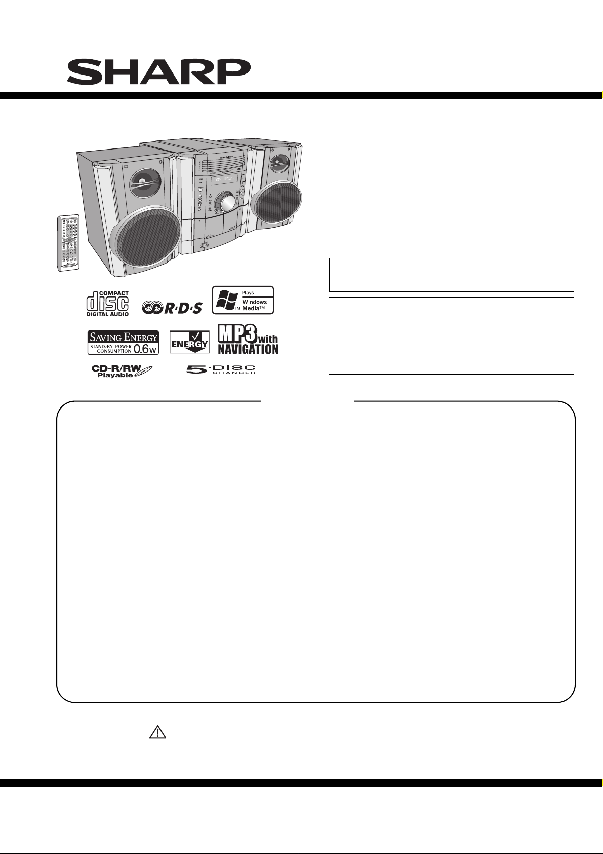
CD-MPX880H
SERVICE MANUAL
No. S4817CDM880HH
MINI COMPONENT SYSTEM
CONTENTS
PRECAUTIONS FOR USING LEAD-FREE SOLDER
CHAPTER 1. GENERAL DESCRIPTION
[1] Safety Precaution For Service Manual........... 1-1
[2] Important Service Notes (for U.K. only) ......... 1-2
[3] Specifications.................................................1-2
[4] Name Of Parts ...............................................1-3
CHAPTER 2. ADJUSTMENTS
[1] Mechanism Section........................................ 2-1
[2] Test Mode.......................................................2-2
[3] CD Section.....................................................2-4
MODEL
[ For Europe, U.K., Australia and New Zealand ]
CD-MPX880H Mini Component System consisting of
CD-MPX880H
system).
• In the interests of user-safety the set should be resto red
to its original condition and only parts identical to those
specified be used.
l
Note for users in U.K.
Recording and playback of any material may require
consent which SHARP is unable to give. Please refer
particularly to the provisions of Copyright Act 1956, the
Performers Protection Acts 1963 and 1972 and
subsequent statutory enactments and orders.
CHAPTER 5. CIRCUIT DESCRIPTION
[1] Waveforms Of CD Circuit ..............................5-1
[2] Voltage...........................................................5-2
CHAPTER 6. CIRCUIT SCHEMATICS AND PARTS
LAYOUT
[1] Notes On Schematic Diagram.......................6-1
[2] Types Of Transistor And LED........................6-1
[3] Schematic Diagram.......................................6-2
[4] Charts Of Connecting Wires........................6-22
[5] Wiring Side Of PWB....................................6-24
CD-MPX880H
(main unit) and CP-MPX880H (speaker
CHAPTER 3. MECHANISM BLOCKS
[1] Caution On Disassembly................................ 3-1
Removing And Reinstalling The Main Parts
[2]
CHAPTER 4. DIAGRAMS
[1] Main Block Diagrams..................................... 4-1
[2] CD Block Diagrams.......................................4-3
Parts marked with " " are important for maintaining the safety of the set. Be sure to replace these parts with
specified ones for maintaining the safety and performance of the set.
..... 3-4
SHARP CORPORATION
CHAPTER 7. FLOWCHART
[1] Troubleshooting.............................................7-1
CHAPTER 8. OTHERS
[1] Function Table Of IC......................................8-1
[2] FL Display......................................................8-8
[3] Wiring Of Primary Supply Leads
(for U.K. only) ................................................8-9
PARTS GUIDE
This document has been published to be used
for after sales service only.
The contents are subject to change without notice.
Page 2
CD-MPX880H
AudioXL-MP150Service ManualXLMP150MarketE
PRECAUTIONS FOR USING LEAD-FREE SOLDER
1. Employing lead-free solder
"MAIN, POWER, DISPLAY, AUDIO IN, CD PWB" of this model employs lead-free solder.
The LF symbol indicates lead-free solder, and is attached on the PWB and service manuals. The alphabetical character
following LF shows the type of lead-free solder.
Example:
Indicates lead-free solder of tin, silver and copper.
2. Using lead-free wire solder
When fixing the PWB soldered with the lead-free solder, apply lead-free wire solder. Repairing with conventional lead wire
solder may cause damage or accident due to cracks.
As the melting point of lead-free solder (Sn-Ag-Cu) is higher than the lead wire solder by 40°C, we recommend you to
use a dedicated soldering bit, if you are not familiar with how to obtain lead-free wire solder or soldering bit, contact our
service station or service branch in your area.
3. Soldering
As the melting point of lead-free solder (Sn-Ag-Cu) is about 220°C which is higher than the conventional lead solder
by 40°C, and as it has poor solder wettability, you may be apt to keep the soldering bit in contact with the PWB for
extended period of time. However, since the land may be peeled of for the maximum heat-resistance temperature
of parts may be exceeded, remove the bit from the PWB as soon as you confirm the steady solder ing condition.
Lead-free solder contains more tin, and the end of the soldering bit may be easily corrected. Make sure to turn on
and off the power of the bit as required.
If a different type of solder stays on the tip of the soldering bit, it is alloyed with lead-free solder. Clean the bit after
every use of it.
When the tip of the soldering bit is blackened during use, file it with steel wool or fine sandpaper.
Be careful when replacing parts with polarity indication on the PWB silk.
Lead-free wire solder for servicing
Ref No.
PWB-A 92LPWB7269MANS MAIN (A1), POWER (A2)
PWB-B 92LPWB7269DPLS DISPLAY (B1), AUDIO IN (B2)
PWB-C 92LPWB6700CDUS CD
Parts No.
Description
– i –
Page 3
CD-MPX880H
CHAPTER 1: GENERAL DESCRIPTION
[1]
Safety Precaution For Service Manual
WARNINGS
THE AEL (ACCESSIBLE EMISSION LEVEL) OF LASER POWER OUTPUT FOR THIS MODEL IS SPECIFIED TO
BE LOWER THAN CLASS I REQUIREMENTS. HOWEVER, THE FOLLOWING PRECAUTIONS MUST BE OBSERVED
DURING SERVICING TO PROTECT YOUR EYES AGAINTS EXPOSURE TO THE LASER BEAM.
1- WHEN THE CABINET HAS BEEN REMOVED, THE POWER IS TURNED ON WITHOUT A COMPACT DISC,
AND THE PICKUP IS ON A POSITION OUTER THAN THE LEAD-IN POSITION, THE LASER WILL LIGHT FOR
SEVERAL SECONDS TO DETECT A DISC.
DO NOT LOOK INTO THE PICKUP LENS.
2- THE LASER POWER OUTPUT OF THE PICKUP INSIDE THE UNIT AND REPLACEMENT SERVICE PARTS
HAVE ALREADY BEEN ADJUSTED PRIOR TO SHIPPING.
3- NO ADJUSTMENT TO THE LASER POWER SHOULD BE ATTEMPTED WHEN REPLACING OR SERVICING
THE PICKUP.
4- UNDER NO CIRCUMSTANCES LOOK DIRECTLY INTO THE PICKUP LENS AT ANY TIME.
5- CAUTION - USE OF CONTROLS OR ADJUSTMENTS, OR PERFORMANCE OF PROCEDURES OTHER THAN
THOSE SPECIFIED HEREIN MAY RESULT IN HAZARDOUS RADIATION EXPOSURE.
This product is classified as a CLASS 1 LASER PRODUCT.
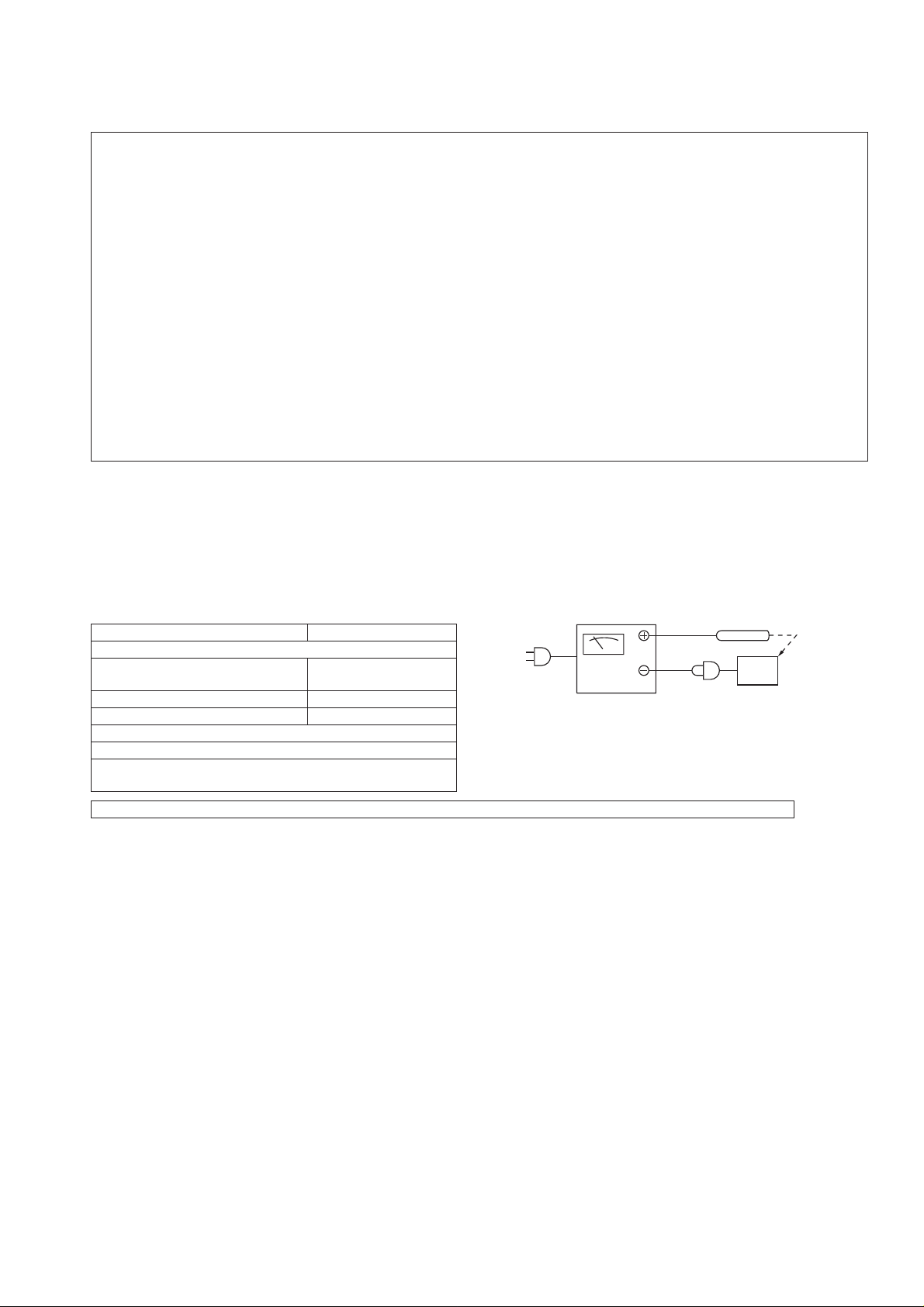
[2] Important Service Notes (For U.K. Only)
Before returning the unit to the customer after completion of a repair or adjustment it is necessary for the following withstand voltage test to be
applied to ensure the unit is safe for the customer to use.
Setting of Withstanding Voltage Tester and set.
Set name set value
Withstanding Voltage Tester
Test voltage 4,240 VPEAK
3,000 VRMS
Set time 6 secs
Set current (Cutoff current) 4 mA
Unit
Judgment
OK: The “GOOD” lamp lights.
NG: The “NG” lamp lights and the buzzer sounds.
FOR A COMPLETE DESCRIPTION OF THE OPERATION OF THIS UNIT, PLEASE REFER TO THE OPERATION MANUAL.
WITHSTANDING
VOLTAGE TESTER
AC
OUT
SHORT-CIRCUIT
AC POWER
SUPPLY CORD
PROBE
UNIT
CONNECT THE PROBE
TO GND OF CHASSIS
SCREW
1 – 1
–2
Page 4
CD-MPX880H
[3]
Specifications
CD-MPX880H
General
Power source AC 220 - 240 V ~ 50 Hz
Power consumption
Dimensions Width: 260 mm (10 - 1/4" )
Weight 7.4 kg (16.31 lbs.)
(*) This power consumption value is obtained when the
demonstration mode is cancelled in the power stand-by mode.
Power on: 82 W
Power stand-by: 0.6 W (*)
Height: 332 mm (13" )
Depth: 324 mm (12 - 7/8")
Amplifier
Output power PMPO: 880 W
Output terminals Front Speakers: 6 ohms
Input terminals Audio In (audio signal):
MPO: 440 W (220 W + 220 W) (10 % T.H.D.)
RMS: 280 W (140 W + 140 W) (10 % T.H.D.)
RMS: 200 W (100 W + 100 W) (1 % T.H.D.)
Headphones: 16 - 50 ohms
(recommended: 32 ohms)
250 mV/ 47 k ohms
Tuner
Frequency range FM: 87.5 - 108.0 MHz
AM: 522 - 1,620 kHz
CD player
Type 5-disc multi-play compact disc player
Signal readout Non-contact, 3-beam semiconductor laser
D/A converter 1-bit D/A converter
Frequency
response
Dynamic range 90 dB (1 kHz)
pickup
20 - 20,000 Hz
Cassette deck
Frequency
response
Signal/noise ratio 55 dB (TAPE 1, playback)
Wow and flutter 0.35 % (DIN 45 511)
50 - 14,000 Hz (normal tape)
50 dB (TAPE 2, recording/playback)
Speaker
Type 2-way type speaker system
5 cm (2") tweeter
16 cm (6-5/16") woofer
Maximum input
power
Rated input power 140 W
Impedance 6 ohms
Dimensions Width: 200 mm (7-7/8")
Weight 3.18 kg (7.0 lbs.)/each
280 W
Height: 330 mm (13")
Depth: 220.5 mm (8 - 11/16")
CD-MPX880H for U.K., Australia and New Zealand
General
Power source AC 220 - 240V ~ 50Hz
Power consumption
Dimensions Width: 260 mm (10 - 1/4" )
Weight 7.4 kg (16.31 lbs.)
(*) This power consumption value is obtained when the
demonstration mode is cancelled in the power stand-by mode.
Power on: 82 W
Power stand-by: 0.6 W (*)
Height: 332 mm (13" )
Depth: 324 mm (12 - 7/8")
Amplifier
Output power RMS: 280 W (140 W + 140 W) (10% T.H.D.)
Output terminals Front Spe akers: 6 ohms
Input terminals Audio In (audio signal):
RMS: 200 W (100 W + 100 W) (0.9% T.H.D.)
Headphones: 16 - 50 ohms
(recommended: 32 ohms)
250 mV/ 47 k ohms
Tuner
Frequency range FM: 87.5 - 108.0 MHz
AM: 522 - 1,620 kHz
CD player
Type 5-disc multi-play compact disc player
Signal readout Non-contact, 3-beam semiconductor laser
D/A converter 1-bit D/A converter
Frequency
response
Dynamic range 90 dB (1 kHz)
pickup
20 - 20,000 Hz
Cassette deck
Frequency
response
Signal/noise ratio 55 dB (TAPE 1, playback)
Wow and flutter 0.3% (WRMS)
50 - 14,000 Hz (normal tape)
50 dB (TAPE 2, recording/playback)
Speaker
Type 2-way type speaker system
5 cm (2") tweeter
16 cm (6-5/16") woofer
Maximum input
power
Rated input power 140 W
Impedance 6 ohms
Dimensions Width: 200 mm (7-7/8")
Weight 3.18 kg (7.0 lbs.)/each
280 W
Height: 330 mm (13")
Depth: 220.5 mm (8 - 11/16")
1 – 2
– 4
Page 5
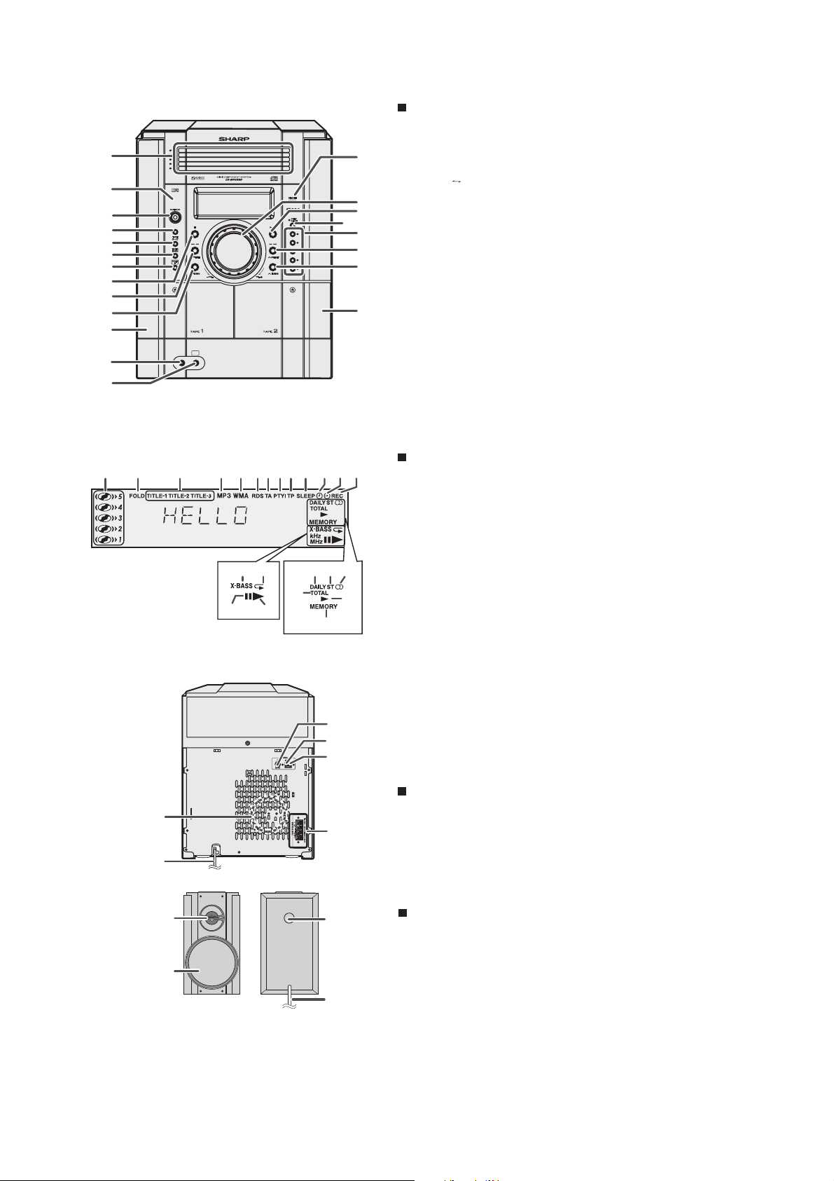
[4] Names Of Parts
5
1
2
3
4
5
6
7
8
9
10
11
12
13
4
3
2
1
TIMER
CD
PLAYBACK
AUDIO
PHONES
CD-MPX880H
Front panel
1. Disc Trays
2. Timer Indicator
3. On/Stand-by Button
14
4. CD Button
5. Tape (1 2) Button
6. Tuner (Band) Button
15
7.Audio In Button
16
5
4
3
2
1
(PLAY & STOP)
IN
RECORD/PLAYBACK
17
8. CD or Tape Stop Button
9. CD Track Down or Fast Reverse, Tape 2 Rewind,
18
Tuner Preset Down, Time Down Button
19
10. Tuning Down Button
20
11. Tape 1 Cassette Compartment
12. Headphone Socket
13. Audio In Socket
21
14. Remote Sensor
15. Volume Control
16. CD Play or Repeat, Tape Play Button
17. Disc Tray Open/Close Button
18. Disc Number Select Buttons
19. CD Track Up or Fast Forward, Tape 2 Fast Forward,
Tuner Preset Up, Time Up Button
20. Tuning Up Button
21. Tape 2 Cassette Compartment
12 3 45678 910111213
20 21
22
23
14
151617
18
19
3
4
5
1
AC INPUT
6
2
Display
1. Disc Number Indicators
2. MP3/WMA Folder Indicator
3. MP3/WMA Title Indicators
4. MP3 Indicator
5. WMA Indicator
6. RDS Indicator
7. Traffic Announcement Indicator
8. Dynamic PTY Indicator
9. Traffic Programme Indicator
10. Sleep Indicator
11. Timer Play Indicator
12. Timer Recording Indicator
13. Tape 2 Record Indicator
14. MP3/WMA Total Indicator
15. Daily Timer Indicator
16. FM Stereo Mode Indicator
17. FM Stereo Receiving Indicator
18. Tape Play Indicator
19. Memory Indicator
20. Extra Bass Indicator
21. Disc Repeat Play Indicator
22. Disc Pause Indicator
23. Disc Play Indicator
Rear panel
1. Cooling Fan
2. AC Power Lead
3. FM 75 Ohms Aerial Socket
4. AM Aerial Earth Terminal
5. AM Loop Aerial Terminal
6. Front Speaker Terminals
1
3
Speaker system
1. Tweeter
2. Woofer
3. Bass Reflex Duct
2
4. Speaker Wire
4
1 – 3
–2
Page 6
CD-MPX880H
1
13
14
8
15
9
10
2
A O
IDU
NI
11
12
3
4
16
22
24
25
26 27 28 29
17
18
19
20
21
23
5
6
7
30 31 32
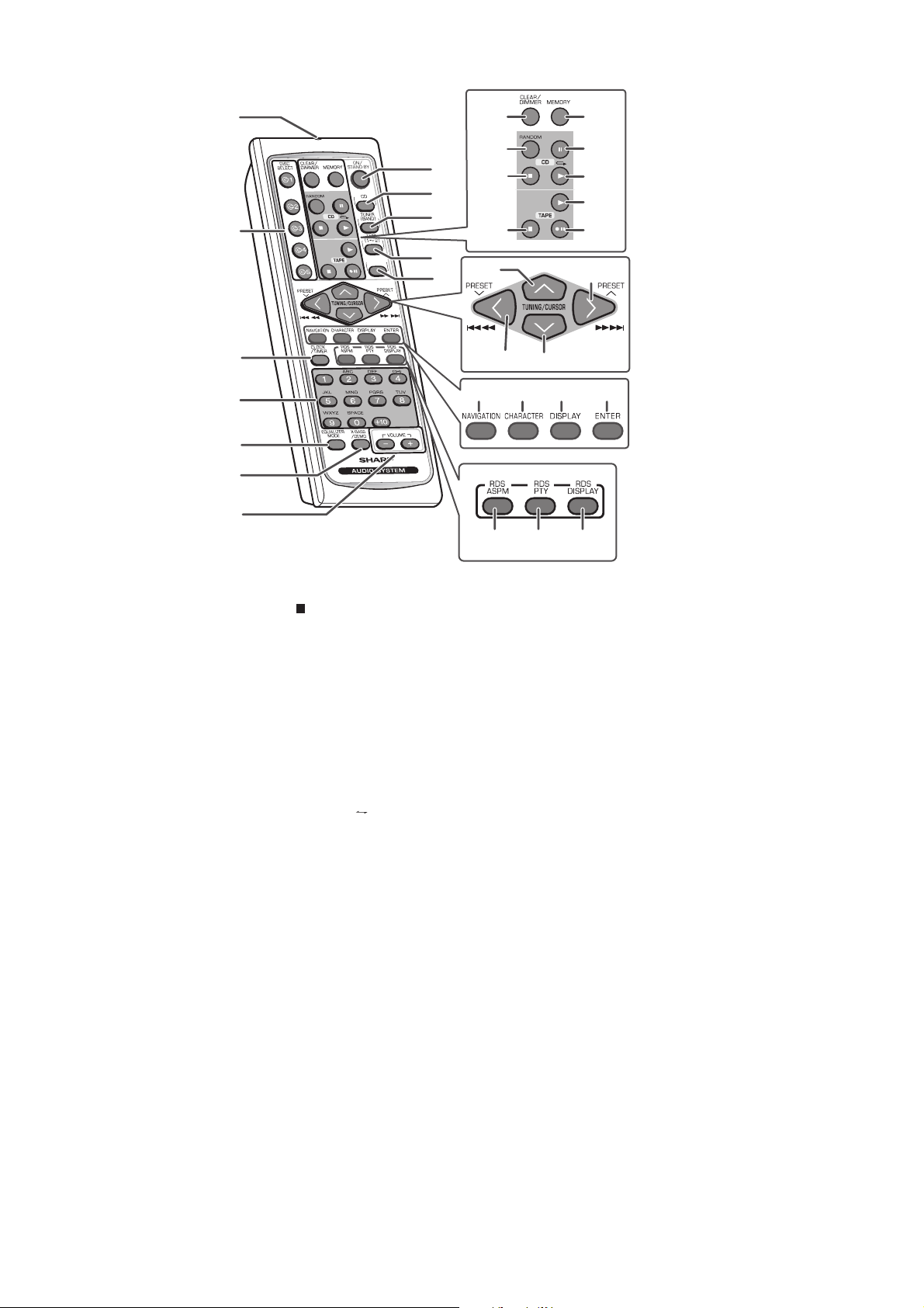
Remote control
1. Remote Control Transmitter
2. Disc Number Select Buttons
3. Clock/Timer Button
4. Character Input/Disc Direct Search Buttons
5. Equaliser Mode Select Button
6. Extra Bass/Demo Button
7. Volume Up and Down Buttons
8. ON/STAND-BY Button
9. CD Button
10. Tuner (Band) Button
11. Tape (1 2) Button
12. AUDIO IN Button
13. Disc Clear/Dimmer Button
14. Disc Random Button
15. Disc Stop Button
16. Tape Stop Button
17. Memory Button
18. Disc Pause Button
19. Disc Play or Repeat Button
20. Tape Play Button
21. Tape 2 Record Pause Button
22. Tuning Up, Cursor Up Button
23. Disc Track Up or Fast Forward, Tape 2 Fast Forward,
Tuner Preset Up, Time Up, Cursor Right Button
24. Disc Track Down or Fast Reverse, Tape 2 Rewind,
Tuner Preset Down, Time Down, Cursor Left Button
25. Tuning Down, Cursor Down Button
26. MP3/WMA Navigation Mode Select Button
27. Character Button
28. MP3/WMA Display Button
29. Enter Button
30. RDS ASPM Button
31. RDS PTY Button
32. RDS Display Button
1 – 4
– 4
Page 7
CD-ES700/CD-ES77CD-ES700/CD-ES77Service ManualCD-ES700/CD-ES77MarketE
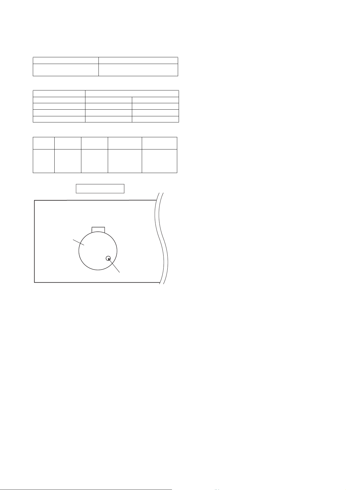
CHAPTER 2. ADJUSTMENTS
[1] Mechanism Section
• Driving Force Check
Torque Meter Specified Value
Play: TW-2111 Tape 1: Over 75 g
Tape 2: Over 75 g
• Torque Check
Torque Meter Specified Value
Tape 1 Tape 2
Play: TW-2111 25 to 85 g.cm 25 to 85 g.cm
FF/REW — 45 to 195 g.cm
BACK TENSION 1.2 to 7.0 g.cm 1.2 to 7.0 g.cm
• Tape Speed
CD-MPX880H
Test Tape Adjusting
Normal
speed
MTT-111 Variable
Tape
Motor
Figure 1
Point
Resistor in
motor.
TAPE MECHANISM
Specified
Value
3,000 ± 90 Hz
Speaker
Variable Resistor in motor
Instrument
Connection
Speaker
T erminal (Load
resistance:
6 ohms)
2 – 1
Page 8
CD-MPX880H
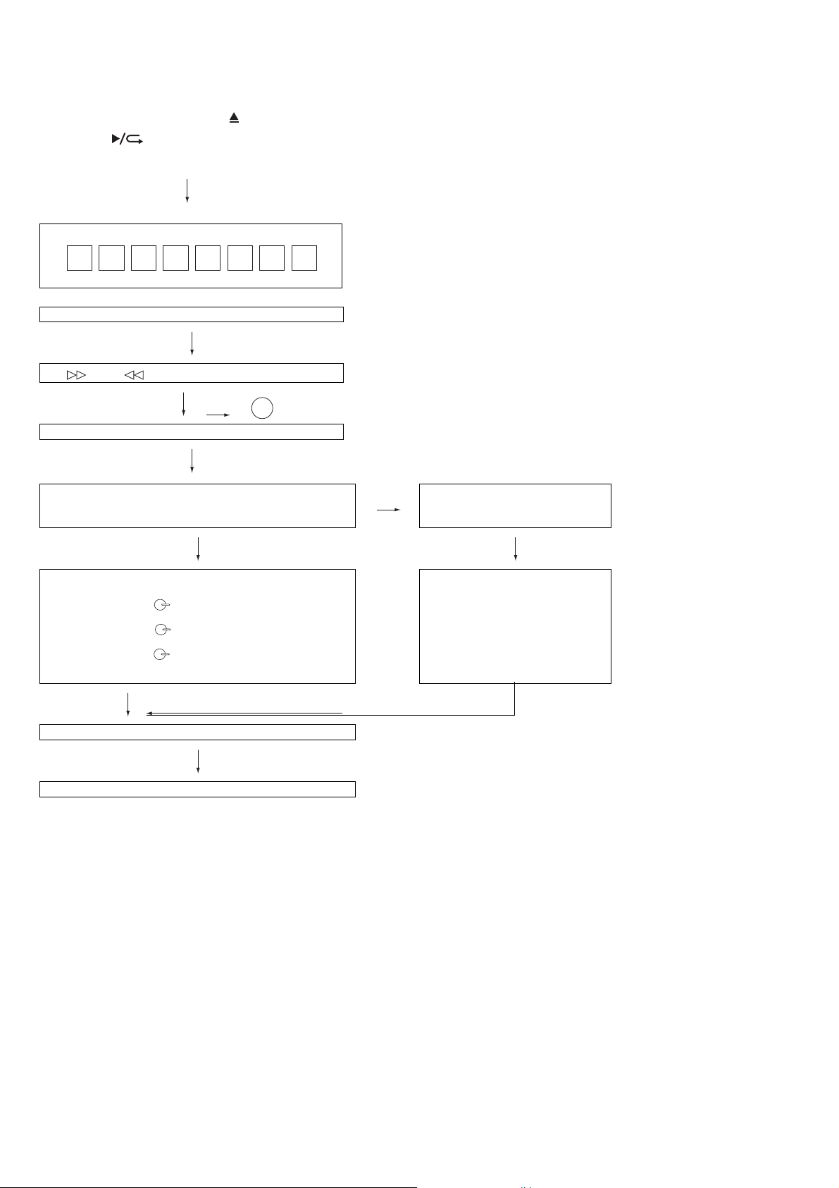
[2] Test Mode
• Setting the test mode
During stand-by mode, press button while pressing
down the button and ON/STAND-BY button.
then, press the CD button to enter the test mode.
C D T E S T
OPEN/CLOSE operation is using manual. IL isn’t done
<< >>,<< >>buttons make pick's slide possible.
to page 2-3
<<PLAY>> key input.
Do TOC IL. Do normal play.
When these following key is input into PLAY key, track
number can be appoint directly.
<< 1>> key: Track 4
<< 2>> key: Track 9
<< 3>> key: Track 15
A
IL isn’t done
IL isn’t done
<<MEMORY>> key input.
Adjustment result automatically will
display as below for each 2 sec:
a) "FOF_XXXX"
b) "TOF_XXXX"
c) "TBAL_XX"
d) "TGAN_XX"
f) "FGAN_XX"
g) "RFLS_XX"
<<STOP>> key input.
STOP
Explanation:
a) Focus off set = "FOF_XXXX"
b) Tracking off set = "TOF_XXXX"
c) Tracking balance = "TBAL_XX"
d) Tracking Gain = "TGAN_XX"
f) Focus Gain = "FGAN_XX"
g) RF level shift = "RFLS_XX"
VOL — Last memory
P.GEQ — FLAT
X-BASS — OFF
To cancel: Power OFF
2 – 2
Page 9
A
<<MEMORY>> key input.
Laser ON.
<<MEMORY>> key input.
Tracking OFF play at that specific point.
<<MEMORY>> key input.
Tracking ON play from that specific point.
CD-MPX880H
<<MEMORY>> key input.
Adjustment result automatically will display as below for each 2 sec :
a) "FOF_XXXX"
b) "TOF_XXXX"
c) "TBAL_XX"
d) "TGAN_XX"
f) "FGAN_XX"
g) "RFLS_XX"
<<STOP>> key input.
STOP
Sliding the PICKUP with << >>, << >> button
must only be in STOP mode.
Explanation:
a) Focus off set = "FOF_XXXX"
b) Tracking off set = "TOF_XXXX"
c) Tracking balance = "TBAL_XX"
d) Tracking Gain = "TGAN_XX"
f) Focus Gain = "FGAN_XX"
g) RF level shift = "RFLS_XX"
VOL — Last memory
P.GEQ — FLAT
X-BASS — OFF
To cancel: Power OFF
2 – 3
Page 10
CD-MPX880H
[3] CD Section
CD Error code description
Error Explanation
10* CAM error. Can't detect CAM switch when CAM is moving.
11* When it detect cam operation error during initialize process.
20* TRAY error . Can't detect TRAY switch when TRAY is moving.
21* When it detect TRAY operation error during initialize process.
31 When it change to CD function, DSP cannot read initial data.
* 'CHECKING'
If Error is detected, 'CHECKING' will be displayed instead of 'ER-CD**'. 'ER-CD**' display will only be displayed
th
when error had been detected for the 5
Standard Specification of Stereo System Error Message Display Content s
Error Contents Display Notes
CD CD Changer Mechanism Error. 'ER-CD**' (*) 10: CAM SW Detection NG during normal operation
CD DSP Communication Error. 'ER-CD31' DSP COMMUNICATION ERROR.
Focus Not Match/IL Time Over. 'NO DISC'
TUNER PLL Unlock. PLL Unlock.
(*) CHECKING:
If CD changer mechanism error is detected, 'CHECKING' will be display instead of 'ER-CD**'. 'ER-CD**' display will
only be display when error had been detected for the 5
Speaker abnormal detection and +B PROTECTION display
times.
FM 87.5 MHz
11: CAM SW Detection NG during initialize process
20: TRAY SW Detection NG during normal operation
21: TRAY SW Detection NG during initialize process
th
times.
In case speaker abnormal detection or +B PROTECTION had occurred, the unit will automatically enter to stand - by
mode and Timer indicator will be flashing as below.
Example : In case of speaker abnormal
FLASHING
OFF
NO. 2
(REPEAT)
TIMER
LED
ON
OFF
NO. 1
NO.1 : +B Protection
NO.2 : Speaker abnormal
OFF
FLASHING
NO. 2
1 FRAME
OFF
ON
NO. 1
+B PROTECTION is condition when irregular process occur on power supply line.
BEFORE TRANSPORTING THE UNIT
The following process need to be taken after set tapering/parts replacement.
1. Press the ON/STAND-BY button to enter stand-by mode.
2. While pressing down the button and the button, press the ON/STAND-BY button. The Micro Computer
version number will be displayed as "CM*****".
3. Press button until "WAIT"→ "FINISHED" appears.
4. Unplug the AC cord and the unit is ready for transporting.
2 – 4
Page 11
CD-MPX880H
CD-ES700/CD-ES77CD-ES700/CD-ES77Service ManualCD-ES700/CD-ES77MarketE
CHAPTER 3. MECHANISM BLOCKS
[1] Caution On Disassembly
Follow the below-mentioned notes when disassembling the unit and reassembling it, to keep it safe and ensure
excellent performance:
1. Take cassette tape and compact disc out of the unit.
2. Be sure to remove the power supply plug from the wall outlet before starting to disassemble the unit.
3. Take off nylon bands or wire holders where the y need to b e r emove d whe n disassembling th e u nit. After servicing
the unit, be sure to rearrange the leads where they were before disassembling.
STEP
1
2
3
4
5
6
7
8
9
10
11
12
13
14
CD Mechanism
REMOVAL
Top Cabinet
Side Panel (Left/
Right)
CD Changer Unit
Rear Panel with
Fan Motor
Front Panel
Main PWB
Power PWB
Tape Mechanism
Game Input PWB
Display PWB
Re-Flash PWB
CD Servo PWB
Changer
Mechanism Unit
PROCEDURE
1. Screw…………..………(A1) X 5
2. Screw……….………….(B1) X 8
1. Hook …………………...(C1) X 2
2. Socket……………….....(C2) X 1
3. Flat Cable ………..……(C3) X 1
1. Screw………….…….....(D1) X 9
1. Screw………………..…(E1) X 3
2. Flat Cable ………..……(E2) X 1
3. Socket……..….............(E3) X 1
4. Hook ……………..........(E4) X 2
1. Screw………………..…(F1) X 3
2. Socket……..…………...(F2) X 4
3. Flat Cable ………..…....(F3) X 1
1. Screw………………......(G1) X 4
1. Screw…….………….....(H1) X 6
2. Flat Cable ………..……(H2) X 1
1. Screw………………..…(J1) X 2
1. Knob……..…………..…(K1) X 1
2. Nut……………..…….....(K2) X 1
3. Washer……..….…........(K3) X 1
4. Screw……..……...........(K4) X 6
1. Screw………….............(L1) X 1
1. Screw...........................(M1) X 2
2. Flat Cable ....................(M2) X 2
3. Socket……...................(M3) X 1
1. Screw…........................(N1) X 4
2. Changer Chassis..........(N2) X 1
1. Screw…........................(P1) X 4
FIGURE
1
1
2
2
2,3
2
2
3
2,3
3
3
3
4
5
5
6
7
8
9
CD Changer
Unit
Rear Panel
(D1)x9
3x10mm
O
Figure 2
CD Servo PWB
PULL
Hook
(C1)x1
Power PWB
Fan Motor
(F2)x1
(E3)x1
(C3)x1
(F2)x2
(C2)x1
Main PWB
(F1)x1
3x10mm
O
Front Panel
(E2)x1
PULL
Lug wire
(E1)x1
3x10mm
O
Hook
(C1)x1
Note:
After removing the connector for the optical pickup from the connector,
wrap the conductive aluminium foil around the front end of the connector
so as to protect the optical pickup from electrostatic damage.
(A1)x2
3x12mm
(B1)x2
3x10mm
(A1)x1
3x12mm
Figure 1
Side Panel
(Right)
(B1)x2
3x10mm
Top Cabinet
Rear Panel
(B1)x2
3x10mm
(B1)x2
3x10mm
Front Panel
Side Panel
(Left)
(A1)x2
3x12mm
Power PWB
Figure 3
(E4)x1
PULL
(G1)x4
4x8mm
(F2)x1
(F3)x1
(F1)x2
3x6mm
O
(E1)x2
3x8mm
O
Front Panel
PULL
Hook
(E4)x1
3 – 1
Page 12
CD-MPX880H
O
O
(H1)x6
O
Tap e
Mechanism
3x10mm
Figure 4
(H2)x1
Lug wire
Front Panel
(N1)x4
3x10mm
(N2)x1
Front Panel
(K4)x6
2.6x10mm
Figure 5
(J1)x2
Special
Display PWB
Nut (K2)x1
(K1)x1
Washer
(K3)x1
Game Input
PWB
(P1)x4
2.6x10mm
CD Mechanism
Figure 8
Changer
Mechanism
Unit
Changer
Mechanism
Unit
Figure 9
Figure 6
(M2)x1
Main Chasis
(M1)x2
3x10mm
(M3)x1
(L1) X 1
3X10mm
Re-Flash PWB
(M2)x1
Figure 7
CD Servo
PWB
Changer
Mechanism
Unit
3 – 2
Page 13
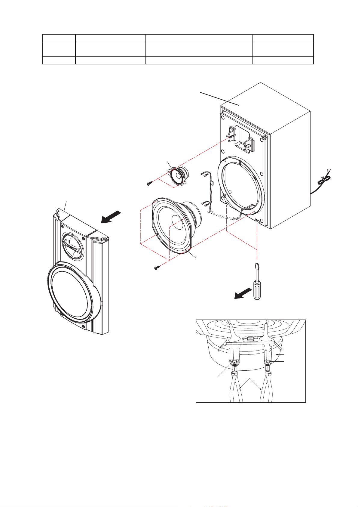
CD-MPX880H
STEP PROCEDURE FIGURE
1 1. Front Panel………….…..(A1) X 1 10
Woofer
REMOVAL
1. Screw…….…….…….….(A2) X 4
2 Tweeter 1. Screw…….……….....….(B1) X 2 10
Speaker Box
Tweeter
(B1) x 2
M3 x 10mm
Front Panel
(A1) x 1
Figure 10
(A2) x 4
M4 x 16mm
Woofer
Screwdriver
SPEAKER UNIT
LOCKING TAB
LOCKING TAB
CAUTION:
TO REMOVE SPEAKER UNIT, PRESS THESE LOCKING TABS
TO RELEASE SPEAKER WIRES.
SPEAKER WIRE
3 – 3
Page 14
CD-MPX880H
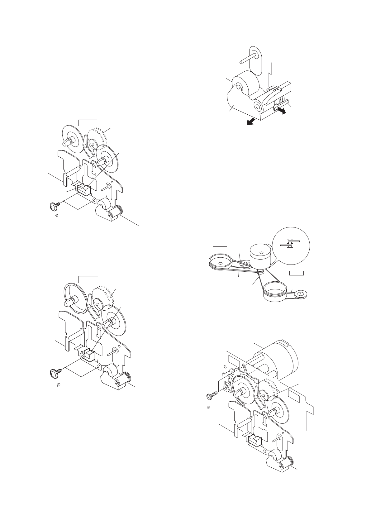
[2] Removing And Reinstalling The Main Parts
1. TAPE MECHANISM SECTION
Perform steps 1 to 3 and 4 of the disassembly method
to remove the tape mechanism.
1.1. How to remove the record/playback and erase
heads (TAPE 2) (See Fig. 1)
1. When you remove the screws (A1) x 2 pcs., the
recording/playback head and three-dimensional
head of the erasing head can be removed.
TAPE 2
Clutch Ass'y
Record/Playback
Head
Pinch
Pinch Roller
(C1)x1
Pull
<B>
<A>
Roller
Pawl
Figure 3
1.4. How to remove the belt (TAPE 2) (See Fig. 4)
1. Remove the main belt (D1) x 1 pc., from the motor
side.
2. Remove the FF/REW belt (D2) x 1 pc.
Erase Head
(A1)x2
2x9mm
Figure 1
1.2. How to remove the playback head (TAPE 1)(See Fig. 2)
1. When you remove the screws (B1) x 2 pcs., the
playback head can be removed.
TAPE 1
Clutch Ass'y
Playback
Head
1.5. How to remove the belt (TAPE 1) (See Fig. 4)
1. Remove the main belt (E1) x 1 pc., from the motor
side.
2. Remove the FF/REW belt (E2) x 1 pc.
Tap e
Motor
TAPE 2
Main Belt
(D1)x1
TAPE 1
Main Belt
(E1)x1
TAPE 1
FF/REW
Belt
(E2)x1
TAPE 2
FF/REW
Belt
(D2)x1
Main Belt
(D1)x1
Main Belt
(E1)x1
Tap e
Motor
Figure 4
1.6. How to remove the motor (See Fig. 5)
1. Remove the screws (F1) x 2 pcs., to remove the motor.
Tap e
Motor
(B1)x2
2x9mm
Figure 2
1.3. How to remove the pinch roller (TAPE 1/2) (See Fig. 3)
1. Carefully bend the pinch roller pawl in the direction
of the arrow <A>, and remove the pinch roller (C1) x
1 pc., in the direction of the arrow <B>.
Note:
When installing the pinch roller, pay attention to the
spring mounting position.
(F1)x2
2.6x5mm
Figure 5
3 – 4
Clutch Ass'y
Page 15
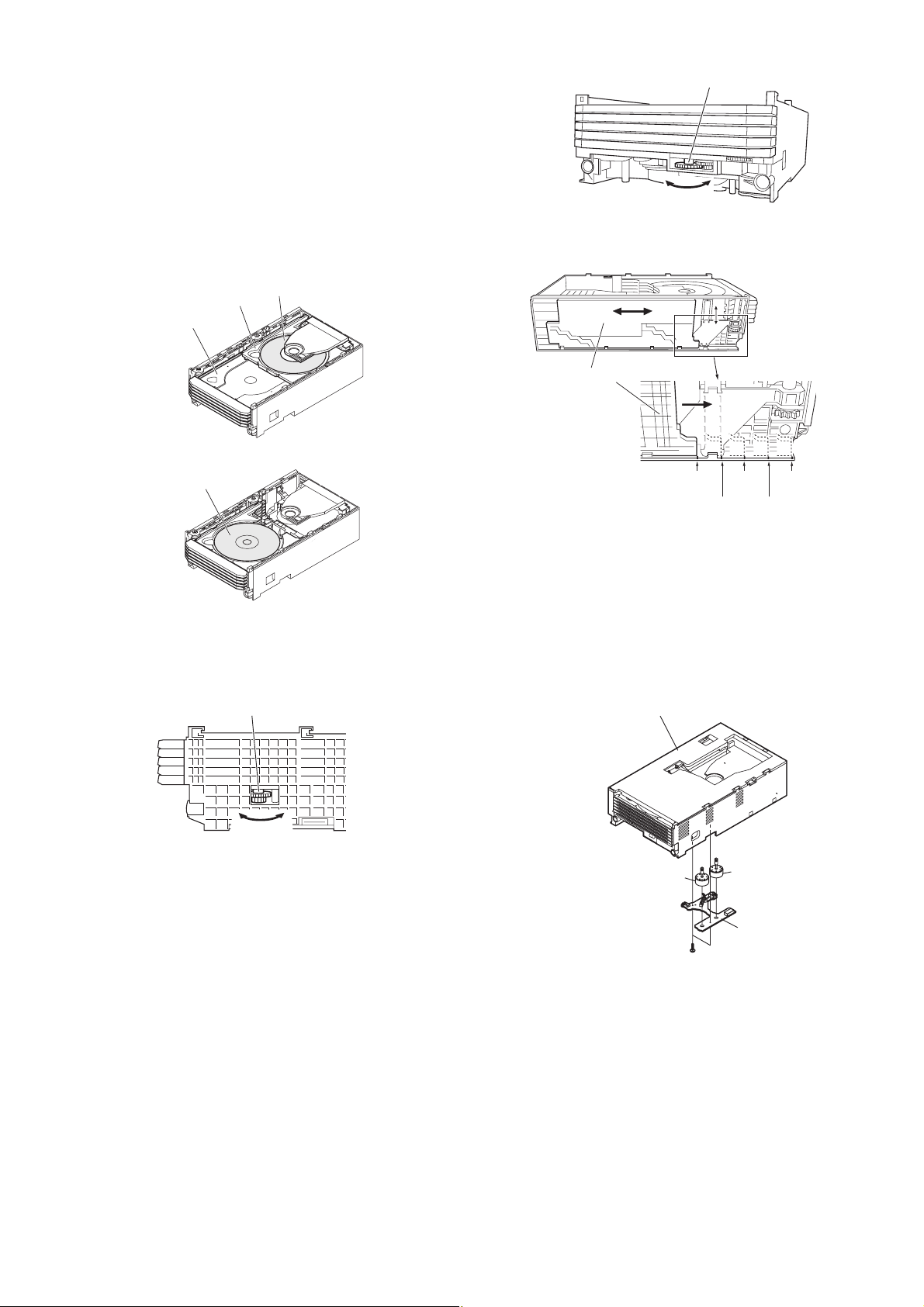
2. CHANGER MECHANISM SECTION
Perform steps 1, 2, 7 and 8 of the disassembly method
to remove the CD changer mechanism.
2.1 How to remove CD Disc (See Fig. 1-4)
1. When CD is at play position (Figure 1), rotate
reduction gear C clock-wise as shown in Figure 2
until disc tray is at stock position, then rotate further
to eject the disc tray so that CD can be removed
from the tray.
CD-MPX880H
Reduction gear D
Up Down
Figure 3
Guide Tray
CD Disc
Disc Tray
Reduction gear C
CD Disc
CD at play position.
CD at stock position.
Figure 1
Gear up down board
Mark 1
(DISC 1)
Figure 4
(DISC 3)
Mark 2
(DISC 2)
Mark 3
(DISC 4)
Mark 4
Mark 5
(DISC 5)
2.2 How to remove the tray motor/main cam motor/
5-Changer Motor PWB (See Fig. 5)
1. Remove the screws (A1)x 2 pcs., to remove tray
motor/main cam motor/5-Changer Motow PWB.
Changer Mechanism Unit
Front Rear
Figure 2
2. In another case, if CD mechanism is at tray No.1
play position and to remove CD located in tray No.3,
the procedure is as follows:
If the gear up down board is located at tray No.1
position, then rotate gear clock-wise until it is at
stock postiiton. Rotate reduction gear D clockwise
(Figure 3) to move the CD mechanism to tray No.3
position. This is confirmed by checking the gear up
down board position by the marking as indicated on
the main chassis as shown in Figure 4.
3 – 5
Main Cam Motor
(A1)x2
φ2x10mm
Figure 5
Tray Motor
5-Changer
Motor PWB
Note:
There are 2 more screws tighten the motors at the
bottom of main chassis. Before performing prodcedure
1 above, disc stop spring, top plate sear up down
board and trays must be removed, then only the 2
screws can be untighten.
Page 16
CD-MPX880H
5
CHAPTER 4. DIAGRAMS
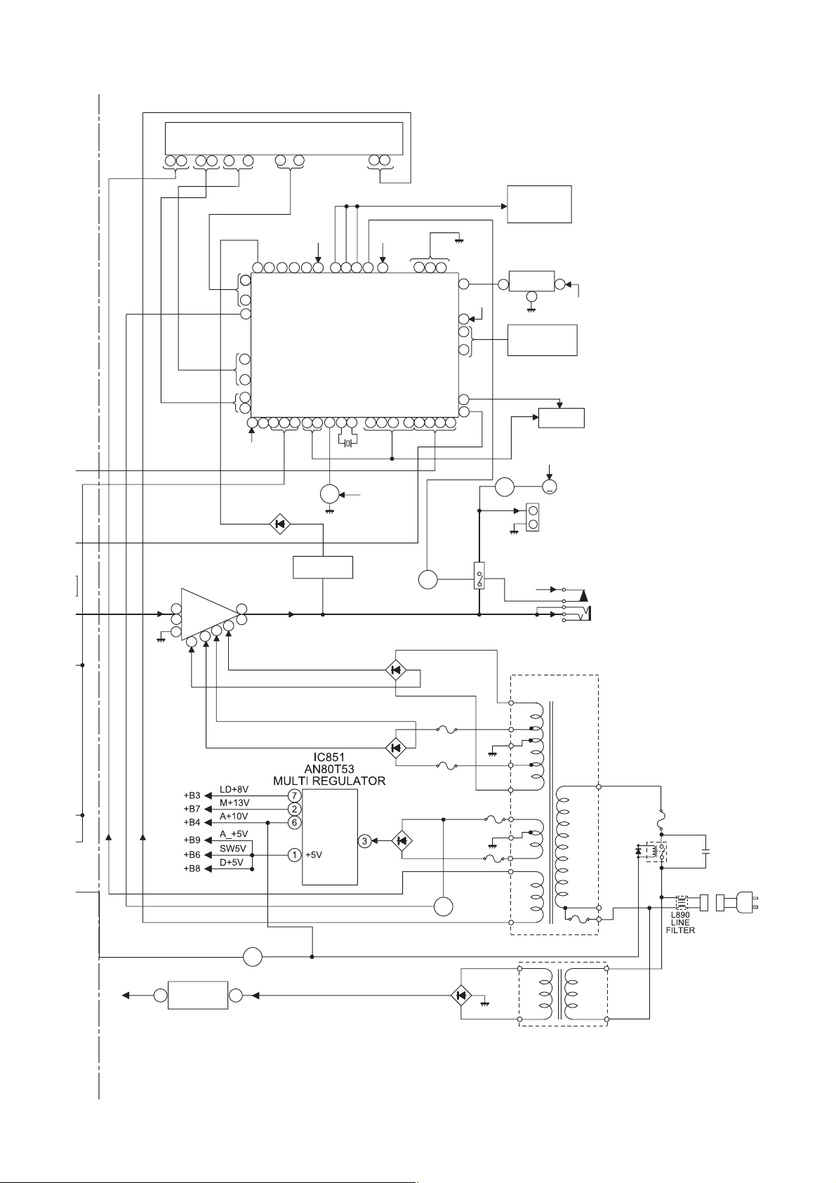
[1] Main Block Diagrams
1
2
3
4
5
6
7
8
9
10
CNP303
(15 PINS)
1
3
4
POP REDUCE
L REC.
R REC.
SWITCHING
Q105
Q106
Q111
L103
BIAS
OSC
11
12
13
14
15
JKA701 (AUDIO IN)
L(T1)
1
24
R(T1)
L(T2)
2
23
R(T2)
6
T1/T2
REC
9
16
11
12
NOR/
15
HIGH
Q114
SWITCHING
+B4
Q112
SWITCHING
CNS603
P.B.
H/N
T1/T2
19
Q113
SWITCHING
+B3
+B3
SOLENOID
FROM CD SECTION
HEAD
L-CH
R-CH
L-CH
R-CH
TAPE 1
P.B. HEAD
TAPE 2
REC./P.B.
MOTOR
DRIVER
Q709~
Q712
Q703~
Q708
DRIVER
CNP2
AC BIAS
ERASE
HEAD
P.B.
REC.
Q609
TAPE
MECHANISM
ASS'Y
BI601CNS601
1
2
3
SWITCHING
Q101~
Q104
L
R
CNP603
13
L
4
21
R
L
7
18
R
10
ALC
+B4
Q109
TUNER
PACK
UNIT
RTUNSA008AWZZ
9
L
16
R
L
10
TAPE
15
R
L
TUNER
+B4
P.B.
REC.
11
14
AUDIO PROCESSOR
R
L
CD
12
13
R
IC101
AN7345K
PLA YBACK AND RECORD/
PLA YBACK AMP.
Q110
BIAS
23
IC601
LC75341
18
3
7
Q107
Q108
MUTING
+B4
1
DI
2
CE
24
CLK
-20dB
ATT
R
21
4
L
MICROCOMPUTER
REC/PLAY
JOG701
VOLUME
5
IC701
IXA180AW
SYSTEM
(2/2)
56
Q607
T1/T2
BIAS
MUTE
SYSTEM
VF1
UN
SW_
+B8
-VF
Figure 4-1: MAIN BLOCK DIAGRAM (1/2)
4 – 1
Page 17
FL701
FL DISPLAY
812 45
26
25
~
CD-MPX880H
+B8
5150
TAPE
MECHANISM
ASS'Y
47
~
+B8
MUTE
SYSTEM
SP DET.
D901~D906
IC901
STK412-410
POWER AMP.
18
L
14
R
7
1
5
2
6
-B1
26 494846 47 3837 394055
57
~
78
80
VLOAD
79
VDD
IXA180AW
MICROCOMPUTER
AVDD
154515253
L-OUT
R-OUT
1011
RESET
Q712
Q901~Q904,
Q906~Q909
11
+B1
81
~
98
99
100
+B8
8
18
VDD
IC701
SYSTEM
(1/2)
RESET
16 1742 1312 20 23 28 29 30 31
XL701
8.388 MHz
+B8
SP RELAY
ON-OFF
D801
~
15 14
AVDD
CLK
CEDIDO
FAN MOTOR
Q905
RL914
27
+B8
41
2
~
4
25
36
DRIVER
RX701
REMOTE
1
SENSOR
3
KEY
SW701-SW706
SW707-SW717
Q906
+B3
HEADPHONES
MAIN POWER
TRANSFORMER
2
TO CD
SECTION
+B5
M901
M
FAN
MOTOR
SO901
SPEAKER
TERMINAL
JKA702
PT801
+B8
VF1
UN
SW_5.6V
+B8
-B2
+B2
VF2
-VF
AC_RLY
IC854
31
KIA78L05
VOLTAGE
REGULATOR
RELAY
DRIVER
Q841
F802
T4A L250V
D802
F801
T4A L250V
D803,
D804
Q801
D842~
D845
F804
T2A L250V
F803
T2A L250V
VOLTAGE
REGULATOR
TRANSFORMER
Figure 4-2: MAIN BLOCK DIAGRAM (2/2)
T.F.
PT841
SUB POWER
D846
F805
T2A L250V
RL841
C844
AC POWER
SUPPLY CORD
AC 220-240V ~ 50Hz
4 – 2
Page 18
CD-MPX880H
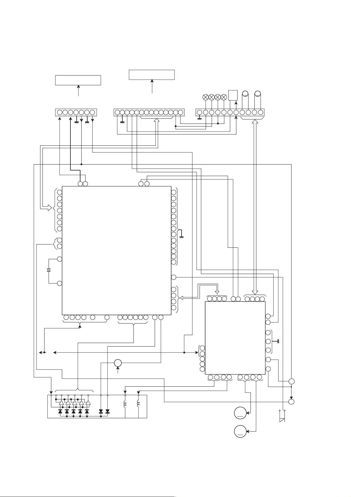
[2] CD Block Diagrams
XL1
16.9344 MHz
+3.3V
CONSTANT
VOLTAGE
TO MAIN SECTION
R-CH
AGND
L-CH
CE
43
CL
44
DI
45
DO
46
RESB
47
INTB0
48
INTB1
49
DVDD 1.8
38
DVDD 1.8
66
XOUT
72
XIN
73
DVDD
AVDD
36 41
+3.3V
D_+5V(+B5)
DGND
7875
LCHO
RCHO
DVDD
DVDD
MGND
+7.5V
7 1 2 3 4 5 6
CNP3
LC78690E
CD SERVO
XVDD
74
TO DISPLAY SECTION
SW3 TRAY SW2
SW2 TRAY SW1
SW1 CLAMP
SW4 DISC
MP3_INT11CD_INT12TRAY SW1/SW2
13
77
71
67
57
56
55
54
53
42
40
37
26
20
32
24
25
22
23
DISC/CLAMP
143 1 9 8 7 6 52 4
+5V
GND
PHOTO
MO_A-
CD_RES
MO_A+
CD_DI
CD_DO
CD_CLK
CD_CE
10
5251
CONT1
CONT0
IC1
PUIN
SLDO
SPDO
FDO
TDO
LDD
EIN
LDS
FIN
18 1968
1413
DIN
BIN
CIN
AIN
LRVDD
76 876521
CNP7
GND
VIN1
VIN2
17151311
VIN3
VIN4
LA6261
FOCUS/TRACKING/
PVCC1
SVCC
PVCC2
VCONT6
VCONT5
SPIN/SLIDE
DRIVER
Q1
+3.3V
LASER
DRIVER
+7.5V
9
27
28
24
21
PHOTO
RX1
22
23
REV6
IC2
M1
5V
M
+
--
FWD6
3363521
4
M2
TRAY MOTOR
M
+
10 113 1 9 8 7 6 52 4
32 3331 34
VO6-
VO6+
FWD5
REV5
REG IN
REG OUT
56
MOTOR
MAIN CAM
CNP4
VO5-
VO5+
19
20
30
7
26
8
10
Q2
+3.3V
COIL
TRACKING
PICKUP UNIT
FOCUS COIL
NM1
SPINDLE
MOTOR
NM2
SLED
MOTOR
M
M
NSW 1
PICKUP
IN
Q3
Figure 4-3: CD BLOCK DIAGRAM
4 – 3
Page 19
CHAPTER 5. CIRCUIT DESCRIPTION
[1] Waveforms Of CD Circuit
CD-MPX880H
1
IC1
22
FDO
1
IC1
2
IC1 IC1
1
IC1 IC1
23
22
TDO
FDO
5
6
7
IC1
3
IC1
16
TE
1
IC1
22
25
28
27
22
FDO
SPDO
PDOUT 0
PDOUT 1
FDO
IC1
IC1
16
TE
4
2
IC1
2
RFOUT
RFOUT
3
4
5 – 1
Page 20
CD-MPX880H
1 1.59 21 3.24 41 3.13 61 1.55
2 0.47 22 1.62 42 0.01 62 1.93
3 0.39 23 1.63 43 0.05 63 1.93
4 2.79 24 1.62 44 2.93 64 1.93
5 1.63 25 1.64 45 2.88 65 0.00
6 1.63 26 0.00 46 1.87 66 1.81
7 1.63 27 0.33 47 3.13 67 0.00
8 1.63 28 1.62 48 3.13 68 3.13
9 1.63 29 1.10 49 3.13 69 0.03
10 1.63 30 3.05 50 0.00 70 0.02
11 1.64 31 0.00 51 3.12 71 0.01
12 0.00 32 3.26 52 3.12 72 1.34
13 1.63 33 0.03 53 0.00 73 1.53
14 1.63 34 0.03 54 0.00 74 3.01
15 1.62 35 0.03 55 0.00 75 1.54
16 1.64 36 3.26 56 0.00 76 3.23
17 1.63 37 0.02 57 0.00 77 0.00
18 3.27 38 1.81 58 0.00 78 1.59
19 0.00 39 2.56 59 1.58 79 3.24
20 0.00 40 0.00 60 1.57 80 1.59
IC 1
PIN NOVOLTAGE
(V)
PIN NOVOLTAGE
(V)
PIN NOVOLTAGE
(V)
PIN NOVOLTAGE
(V)
1 3.43 10 3.28 19 4.51 28 7.64
2 3.50 11 1.65 20 4.50 29 7.58
3 3.44 12 1.65 21 3.45 30 0.00
4 3.48 13 1.65 22 3.10 31 0.00
5 3.44 14 1.65 23 3.10 32 0.00
6 3.49 15 1.65 24 3.09 33 0.00
7 0.00 16 1.65 25 1.65 34 0.00
8 4.20 17 1.65 26 0.02 35 3.49
9 7.63 18 1.65 27 7.64 36 3.45
E 3.26 E 4.86 E 1.81 E 0.00
C 0.10 C 3.27 C 3.26 C 3.28
B 3.23 B 4.19 B 2.33 B 0.00
IC 2
Q 1
Q 2
Q 3
Q 4
VOLTAGE
(V)
PIN NOVOLTAGE
(V)
PIN NOVOLTAGE
(V)
PIN NOVOLTAGE
(V)
PIN NOVOLTAGE
(V)
PIN NOVOLTAGE
(V)
PIN NOVOLTAGE
(V)
PIN NOVOLTAGE
(V)
PIN
NO
[2] Voltage
IC701
PIN PIN
VOLTAGE
NO NO
(V) (V)
1 4.94 V
4.94 V
2 52 4.40 V
353
4.92 V
4.92 V
454
1.32 V
555
4.92 V
656
4.92 V
7 57 -29.05 V
8 0.00 V
9 4.87 V
4.87 V
10 60
4.87 V
11 61
0.00 V
12 62
0.00 V
13 63
0.00 V
14 64
0.00 V
15 65
0.00 V
16 66
0.00 V
17 67
18 68
0.00 V
0.00 V
19 69
20 70
0.00 V
0.00 V
21 71
22 4.52 V 72
23 4.41 V 73
24 4.54 V
0.00 V
25 75
0.00 V
26 76
27 1.87 V 77
4.05 V
28 78
4.07 V
29 79
0.00 V
30 80
31 4.66 V 81
32 0.23 V 82
33 4.95 V 83
34 4.95 V 84
35 85
0.00 V
0.00 V
36 86
37 13.15 V
13.15 V
38 88
13.15 V
39 89
0.00 V
40 90
41 -23.60 V 91
42 4.72 V 92
43 4.41 V
4.54 V
44 94
45 0.00 V 95
0.00 V
46 96
0.00 V
47 97
0.00 V
48 98
49 4.54 V 99
50 0.00 V 100
VOLTAGE
51
58
59
74
87
93
0.00 V
4.38 V
0.00 V
4.39 V
4.43 V
-26.42 V
-18.41 V
-29.08 V
-29.08 V
0.00 V
-29.08 V
-0.92 V
-0.96 V
-11.10 V
0.00 V
-23.60 V
-29.00 V
-23.60 V
0.00 V
0.00 V
-23.60 V
-26.20 V
-23.60 V
0.00 V
-26.40 V
0.00 V
-23.60 V
0.00 V
-23.61 V
-20.84 V
-10.43 V
-23.50 V
-26.40 V
-28.93 V
-26.40 V
-21.10 V
-25.12 V
-24.99 V
-23.01 V
-25.00 V
-24.98 V
-25.00 V
-24.85 V
-24.92 V
-24.89 V
-24.82 V
-24.87 V
-24.63 V
IC 601
PIN
VOLTAGE
NO
10
20
30
4 4.98
5 4.95
6 4.96
7 4.99
8 4.96
9 4.96
10 4.99
11 4.96
12 4.96
13
14 4.96
15 4.96
16 4.96
17 4.99
18 4.96
19 4.96
20 4.96
21 4.96
22 4.98
23 9.95
24 0
4.96
IC 901
PIN
VOLTAGE
NO
1 53.7
2 22.7
3 10.7
4 -10.7
5 -22.7
6 -53.7
70
80
90
10 0
11 0
12 -52.2
13 52.4
14 0
15 0
16 -51
17 0
18 0
5 – 2
IC101
PIN
VOLTAGE
(V)(V)(V)
NO
10
20
30
42
52
6 1.32
70
8 0.6
9 3.48
10 3.44
11 0
12 0
13 6.9
14 4.18
15 0
16 3.45
17 0.6
18 0
19 2.59
20 2
21 2
22
23 0
24 0
0
IC 851
PIN
VOLTAGE
(V)
NO
1 5.06
2 12.83
3 19.6
40
5 18.28
6 9.92
7 8.4
Page 21
CD-MPX880H
CHAPTER 6. CIRCUIT SCHEMATICS AND PARTS LAYOUT
[1] Notes On Schematic Diagram
• Resistor:
To differentiate the units of resistors, such symbol
as K and M are used: the symbol K means 1000
ohm and the symbol M means 1000 kohm and the
resistor without any symbol is ohm-type resistor.
Besides, the one with “Fusible” is a fuse type.
• Capacitor:
To indicate the unit of capacitor, a symbol P is used:
this symbol P means pico-farad and the unit of the
capacitor without such a symbol is micr ofarad. As to
electrolytic capacitor, the expression “capacitance/
withstand voltage” is used.
(CH), (TH), (RH), (UJ): Temperature compensation
(ML): Mylar type
(P.P.): Polypropylene type
• Schematic diagram and Wiring Side of P.W.Board
for this model are subject to change for improvement without prior notice.
• The indicated voltage in each section is the one
measured by Digital Multimeter between such a
section and the chassis with no signal given.
1. In the tuner section,
indicates AM
indicates FM stereo
2. In the main section, a tape is being played back.
3. In the deck section, a tape is being played back.
( ) indicates the record state.
4. In the power section, a tape is being played back.
5. In the CD section, the CD is stopped.
• Parts marked with “ “ ( ) are impor-
tant for maintaining the safety of the set. Be sure to
replace these parts with specified ones for maintaining the safety and performance of the set.
REF. NO DESCRIPTION POSITION
JOG701 VOLUME MAX—MIN
SW701 POWER ON /STAND-BY ON—OFF
SW702 CD ON—OFF
SW703 TAPE ON—OFF
SW704 TUNER (BAND) ON—OFF
SW705 PLAY ON—OFF
SW706 STOP ON—OFF
SW707 FAST REWIND/PRESET DOWN ON—OFF
SW708 TUNING DOWN ON—OF F
[2] Types Of Transistor And LED
FRONT
VIEW
E C B
(S)(G)(D)
(1)(2)(3)
KTA1271 Y
KTA1273 Y
KTA1274 Y
KIA78L05
KTC3199 GR
KTC3200 GR
KTC3203 Y
B
(3)
E
(1)
KTA1504 GR
KRA107 S
KRC102 S
KRC104 S
KTA1504 Y
KTC3875 GR
REF. NO DESCRIPTION POSITION
SW709 FAST FORWARD/PRESET UP ON—OFF
SW710 OPEN/CLOSE ON—OFF
SW711 DISC 5 ON—OFF
SW712 DISC 4 ON—OFF
SW713 DISC 3 ON—OFF
SW714 DISC 2 ON—OFF
SW715 DISC 1 ON—OFF
SW716 TUNING UP ON—OFF
SW717 AUDIO IN ON—OFF
TOP VIEW
TOP
VIEW
(2)
C
MA111
1N4004
DRL204F
HSS4148
TOP VIEW
KDS184
FRONT
VIEW
AC AC
D10XB60F
6 – 1
FRONT
VIEW
SLR342VC
Page 22
CD-MPX880H
[3] Schematic Diagram
A
NC
FM SIGNAL
CD SIGNAL
B
AUDIO SIGNAL
PLAYBACK SIGNAL
RECORD SIGNAL
NC
NC
NC
C
NC
NC
D
E
F
G
H
1
23456
Figure 6-1: MAIN SCHEMATIC DIAGRAM (1/6)
6 – 2
Page 23
CD-MPX880H
7
8 9 10 11 12
Figure 6-2: MAIN SCHEMATIC DIAGRAM (2/6)
6 – 3
Page 24
CD-MPX880H
13
14 15 16 17 18
Figure 6-3: MAIN SCHEMATIC DIAGRAM (3/6)
6 – 4
Page 25
CD-MPX880H
A
B
C
D
E
F
G
H
1
23456
Figure 6-4: MAIN SCHEMATIC DIAGRAM (4/6)
6 – 5
Page 26
CD-MPX880H
7
8 9 10 11 12
Figure 6-5: MAIN SCHEMATIC DIAGRAM (5/6)
6 – 6
Page 27
CD-MPX880H
NC
NC
NC
NC
NC
NC
WZX26AW
13
14 15 16 17 18
Figure 6-6: MAIN SCHEMATIC DIAGRAM (6/6)
6 – 7
Page 28

CD-MPX880H
A
FM SIGNAL
POWER AMP SECTION
B
C
D
E
F
G
H
1
23456
Figure 6-7: MAIN (POWER AMP) SCHEMATIC DIAGRAM (1/4)
6 – 8
Page 29
TO
H/PHONE PWB
CD-MPX880H
7
8 9 10 11 12
Figure 6-8: MAIN (POWER AMP) SCHEMATIC DIAGRAM (2/4)
6 – 9
Page 30

CD-MPX880H
A
B
C
D
E
F
G
H
1
23456
Figure 6-9: MAIN (POWER AMP) SCHEMATIC DIAGRAM (3/4)
6 – 10
Page 31
CD-MPX880H
7
8 9 10 11 12
Figure 6-10: MAIN (POWER AMP) SCHEMATIC DIAGRAM (4/4)
6 – 11
Page 32

CD-MPX880H
A
CD-MPX880H
B
C
D
TO MAIN PWB-A1
E
When Servicing, pay attention as the
area enclosed by this line( )
is directly connected with AC main
voltage.
AC POWER SUPPLY CORD
AC 220-240V ~ 50Hz
F
G
H
TO DISPLAY SECTION
1
23456
Figure 6-11a: POWER SCHEMATIC DIAGRAM
6 – 12
Page 33

A
CD-MPX880H
for U.K., Australia and New Zealand
B
C
CD-MPX880H
D
TO MAIN PWB-A1
E
F
G
TO DISPLAY SECTION
AC POWER SUPPLY CORD
AC 220-240V ~ 50Hz
H
1
23456
Figure 6-11b: POWER SCHEMATIC DIAGRAM
6 – 13
Page 34

CD-MPX880H
A
B
22K
330P
330P
27K
27K
C
22K
D
E
F
G
RDS_DATA/MIC_SW
RDS_CLK
TUN SM (SPAN)
H
1
23456
RDS_VOLT_CONT
AC_RLY
AC_RLY
Figure 6-12: DISPLAY SCHEMATIC DIAGRAM (1/6)
6 – 14
Page 35

CD-MPX880H
D704 SS4148
D702 SS4148
1K
R727 1K
R740 1K
R725
RDS_CLK
RDS_DATA/MIC_SW
7
8 9 10 11 12
Figure 6-13: DISPLAY SCHEMATIC DIAGRAM (2/6)
6 – 15
Page 36

CD-MPX880H
TUN_SM
13
14 15 16 17 18
Figure 6--14: DISPLAY SCHEMATIC DIAGRAM (3/6)
6 – 16
Page 37

CD-MPX880H
A
RDS_DATA/MIC_SW
RDS_CLK
TUN SM (SPAN)
RDS_VOLT_CONT
AC_RLY
AC_RLY
B
C
D
CNP701A
WZY26W
TAPE MECHA SECTION
E
F
CNS702
A935AW
G
H
CNP702
WZY07AW
D707
SS4148
1
23456
Figure 6-15: DISPLAY SCHEMATIC DIAGRAM (4/6)
6 – 17
Page 38

CD-MPX880H
1K
R727 1K
RDS_DATA/MIC_SW
R725
RDS_CLK
R740 1K
D707
SS4148
D708
7
MA111
8 9 10 11 12
Figure 6-16: DISPLAY SCHEMATIC DIAGRAM (5/6)
6 – 18
Page 39

CD-MPX880H
NC
13
14 15 16 17 18
Figure 6-17: DISPLAY SCHEMATIC DIAGRAM (6/6)
6 – 19
Page 40

CD-MPX880H
CD SIGNAL
CNS2B
CNS2A
Figure 6-18: CD SCHEMATIC DIAGRAM (1/2)
6 – 20
Page 41

CD-MPX880H
Figure 6-19: CD SCHEMATIC DIAGRAM (2/2)
6 – 21
Page 42

CD-MPX880H
CNS971
A
FW901
[4] Charts Of Connecting Wires
A
FROM TAPE 1
PLAYBACK HEAD
FROM TAPE 2
RECORD / PLAYBACK HEAD
B
C
GR
WH
BK
BL
GR
WH
BK
PK
WH
BK
BL
GR
WH
BK
PK
WH
BK
GR
WH
BK
234567
1
CNS102
MAIN PWB-A1
CNS101
123
BL
WH
BL
WH
BL
WH
BL
WH
BL
RD
123
CNP101
234567
1
CNP102
Bi801
234567891011
1
FROM
DISPLAY PWB-B1
(CNP701A)
FFC701
26 1 1 15
20 22 24 26
19 21 23 25
18
17
16
15
14
13
12
11
10
9
8
7
6
5
4
3
2
1
CNP701B
1234567
Bi601
123456789
CNP303
10 12 14
11 13 15
Bi601
CNP971
12345678
FM
CNS01CNS02CNP501
CNP603
SUBWOOFER
SO902
F
FRONT SPEAKER
CNP901
TO
15
1012131415161718
CNP701A
FFC701
126
12345678911
15
DISPLAY PWB-B1
D
MAIN PWB-A1
(CNP701B)
E
19212325
20222426
F
1
RD
234567
GR
YL
GR
YL
CNP703
G
123456789111013
FFC703 FFC702
12 14
141110
CNP702
10
123456789
Bi702
GR
TO
H
1
23456
TAPE PWB ASS’Y
Figure 6-20: WIRING CONNECTION (1/2)
6 – 22
Page 43

CD-MPX880H
ER
EAKER
ANTENNA
FM
GND
AM
CNS971
RD
BR
FAN MOTOR
15
FW901
TUNER PACK (TP1)
123
CNS603
PK
BK
WH
GY
PK
BK
WH
12 43
Bi603
15
AUDIO IN PWB-B2
15
FFC303
1
15
TO
PICK UP UNIT
FFC1
CD PWB-C
CNP1
COLOR TABLE
CNS601
RD
GRBLGRBLGR
RD
BK
BL
FFC703
GY
YL
BR
GR
PK
WH
BL
RED
BLACK
GRAY
YELLOW
BROWN
GREEN
PINK
WHITE
BLUE
POWER PWB-A2
12345 6
12
BR
BL
7
8 9 10 11 12
AC POWER SUPPLY CORD
AC 220-240V ~ 50Hz
Figure 6-21: WIRING CONNECTION (2/2)
6 – 23
Page 44
CD-MPX880H
5
[5] Wiring Side Of PWB
MAIN PWB-A1
EC B
ECB
ECB
ECB
ECB
1234567
123
21 23 25
1113 15 17 19
579
13
20 22 24 26
10 12 14 16 18
2468
765432 1
246
13
57
54321
123 4567891011
2134
Lead-free solder indication
Lead-free solder is used in the MAIN PWB.
Refer to "Precautions for handling lead-free solder" for instructions
and precautions.
Figure 6-22: WIRING SIDE OF MAIN PWB (TOP VIEW) (1/2)
6 – 24
Page 45

2468
13579
1013121514
11
CD-MPX880H
2
345 678 9101112131415161718
1 23
JK691
VIDEO OUT
1 2
EC B
EC B
SO901
Figure 6-23: WIRING SIDE OF MAIN PWB (TOP VIEW) (2/2)
6 – 25
SPEAKER TERMINAL
Page 46

CD-MPX880H
MAIN PWB-A1
Lead-free solder indication
Lead-free solder is used in the MAIN PWB.
Refer to "Precautions for handling lead-free solder" for instructions
and precautions.
Figure 6-24: WIRING SIDE OF MAIN PWB (BOTTOM VIEW) (1/2)
6 – 26
Page 47

CD-MPX880H
Figure 6-25: WIRING SIDE OF MAIN PWB (BOTTOM VIEW) (2/2)
6 – 27
Page 48

CD-MPX880H
CD-MPX880H
POWER PWB-A2
PT841
3
4
1
T.F.
ECB
2
1
234567
RL841
891011121314151617
Lead-free solder indication
Lead-free solder is used in the POWER PWB.
Refer to "Precautions for handling lead-free solder"
for instructions and precautions.
Figure 6-26a: WIRING SIDE OF POWER PWB (TOP VIEW)
ECB
When Servicing, pay attention as the
area enclosed by this line( )
is directly connected with AC main
voltage.
2
1
3456
12345678910
6 – 28
Page 49

CD-MPX880H
for U.K., Australia and New Zealand
POWER PWB-A2
CD-MPX880H
PT841
3
4
1
T.F.
ECB
2
1
234567
RL841
891011121314151617
Lead-free solder indication
Lead-free solder is used in the POWER PWB.
Refer to "Precautions for handling lead-free solder"
for instructions and precautions.
Figure 6-26b: WIRING SIDE OF POWER PWB (TOP VIEW)
6 – 29
ECB
2
1
3456
12345678910
Page 50

CD-MPX880H
DISPLAY PWB-B1
A
B
19212325
20222426
R740
365871091211141316151817
214
C
R746
D
R725
E
F
G
Lead-free solder indication
Lead-free solder is used in the DISPLAY PWB.
H
Refer to "Precautions for handling lead-free solder" for
instructions and precautions.
1
23456
Figure 6-27: WIRING SIDE OF DISPLAY PWB (TOP VIEW) (1/2)
6 – 30
123456789
10
14
1098765432111213
Page 51
CD-MPX880H
0
R707
BCE
ECB
987654321
ECB
7
8 9 10 11 12
123456
Figure 6-28: WIRING SIDE OF DISPLAY PWB (TOP VIEW) (2/2)
6 – 31
Page 52

CD-MPX880H
DISPLAY PWB-B1
A
B
C
D
E
F
G
Lead-free solder indication
Lead-free solder is used in the DISPLAY PWB.
H
Refer to "Precautions for handling lead-free solder" for
instructions and precautions.
1
23456
Figure 6-29: WIRING SIDE OF DISPLAY PWB (BOTTOM VIEW) (1/2)
6 – 32
Page 53

CD-MPX880H
7
8 9 10 11 12
Figure 6-30: WIRING SIDE OF DISPLAY PWB (BOTTOM VIEW) (2/2)
6 – 33
Page 54

CD-MPX880H
AUDIO IN PWB-B2
HEADPHONE
AUDIO IN
1234
Lead-free solder indication
Lead-free solder is used in the AUDIO IN PWB.
Refer to "Precautions for handling lead-free solder" for
instructions and precautions.
Figure 6-31: WIRING SIDE OF AUDIO IN PWB (TOP VIEW)
6 – 34
Page 55

AUDIO IN PWB-B2
CD-MPX880H
Lead-free solder indication
Lead-free solder is used in the AUDIO IN PWB.
Refer to "Precautions for handling lead-free solder" for
instructions and precautions.
Figure 6-32: WIRING SIDE OF AUDIO IN PWB (BOTTOM VIEW)
6 – 35
Page 56

CD-MPX880H
N
R10
R25
CD PWB-C
WIRE_A
C27
C22
C36
C8
C42
C6
R7
R2
C20
C7
R5
R3
C4
R6
CNP1
C5
R1
R4
C25
C1
R23
13579111315
246810121416
R13
R24
Lead-free solder indication
Lead-free solder is used in the CD PWB.
Refer to "Precautions for handling lead-free solder" for instructions
and precautions.
C46
R17
C41
C44
C43
C29
C35
R54
XL1
CNP3
R53
R66
R35
R40
R41
R42
C11
R29
C
Figure 6-33: WIRING SIDE OF CD PWB (TOP VIEW) (1/2)
6 – 36
Page 57

CD-MPX880H
13
24
C1
R23
R13
R24
R35
C3
R10
R25
R12
R9
R27 R11
WIRE_A’
Q2
C58
R20
R19
R21
R22
R26
123456
C57
CNP2
J29
C10
CNP4
R62
40
1
CNP7
R57
Figure 6-34: WIRING SIDE OF CD PWB (TOP VIEW) (2/2)
6 – 37
Page 58
CD-MPX880H
CD PWB-C
R8
JP10
R28
JP9
R61
R60
R59
R58
JP1
IC2
JP12
JP21
JP11
R63
C21
R33
R34
C9
C51
R64
C53
C54
C23
C24
JP2
C31
R32
C50
C52
R36
R55
JP3
R37
C26
TP5
JP14
R38
JP17
R15
R14
JP7
JP8
C55
C56
R39
Q4
C2
JP15
R44
C33
R43
JP6
R68
R67
C37
JP20
R65
JP16
D1
C18
TP4
JP18
IC1
TP3
R46
C34
R45
C32
JP19
C28
TP1
1
C17
C16
C15
C59
FB2
TP2
R47
JP13
C49
Q1
C47
R16
R48
C13
C12
R31
C14
R30
C48
C30
C19
C40
FB1
Q3
R18
R52
C45
R49
R50R51
Lead-free solder indication
Lead-free solder is used in the CD PWB.
Refer to "Precautions for handling lead-free solder" for instructions
and precautions.
Figure 6-35: WIRING SIDE OF CD PWB (BOTTOM VIEW)
6 – 38
Page 59

CD-MPX880H
CHAPTER 7. FLOWCHART
[1] Troubleshooting
1. When the CD does not function
The CD section may not operate when the objective lens of the optical pickup is dirty. Clean the objective lens, and
check the playback operation. When this sec tion does not operate even af ter the abo ve step is t ak en, che ck the fo llowing items.
Remove the cabinet and follow the trouble shooting instructions.
"Track skipping and/or no T OC (Table Of Contents) may be caused by build up of dust other foreign matter on the laser
pickup lens. Before attempting any adjustmen t ma ke certain that the lens is clean. If not, clean it as mentioned below."
Turn the power off.
Gently clean the lens with a lens cleaning tissue and a small amount of isopropyl alcohol.
Do not touch the lens with the bare hand.
Parts code
1. CD optical pickup Lens cleaner disc UDSKA0004AFZZ
HOW TO USE
Using the brush in the cleaner cap, apply 1 or 2 drops of the cleaning fluid to the
1.
brush on the CD cleaner disc which has the mark next to it.
Place the CD cleaner disc onto the CD disc tray with the brush side down, then
2.
press the play button.
You will hear music for about 20 seconds and the CD player will automatically stop.
3.
If it still play continuously, press the stop button.
CAUTION
The CD lens cleaner should be effective for 30-50 operations, however if the
brushes become worn out earlier then please replace the cleaner disc.
If the CD cleaner brushes become very wet then wipe off any excess fluid with a soft
cloth.
Do not drink the cleaner fluid or allow it contact with the eyes. In the event of this
happening then drink and / or rinse with clean water and seek medical advice.
The CD cleaner disc must not be used on car CD players or on computer CD-ROM
drives.
All rights reserved. Unauthorized duplicating, broadcasting and renting this product
is prohibited by law.
2. When a CD cannot be played
Cleaning fluid
Cleaner disc
2.1. Pressing the CD operation key is accepted, but playback does not occur.
1) Focus-HF system check
2) Tracking system check
3) Spin system check
4) PLL system check
7 – 1
Page 60

CD-MPX880H
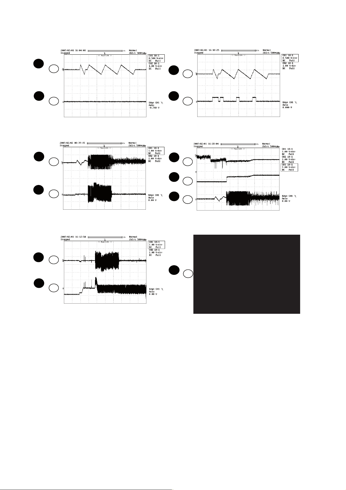
(1) Focus-RF system check.
Although a CD is inserted and the cover is closed,
"NO DISC" is displayed.
Press the Tray1 CD Eject Button without inserting a disc, and try
starting the playback operation.
1
IC1
22
FDO
2
IC1
1. Does the pickup move to the PICKUP-IN Switch (NSW1)
position ?
Yes
2. Does the focus (lens) move up and down ?
(Waveform drawing Figure 1)
Yes
3. Is the laser lit ? No Check the laser diode driver Q1 peripheral circuit.
Yes
4. Is the turntable rotating ? No Spindle motor (NM1).
When a disc is loaded, start playback operation.
No Sled motor (NM2).
No Check the focus peripheral circuit.
23
TDO
Figure 1
1. Is focus servo activated ?
(Waveform drawing Figure 2)
Yes
2. Is the RF waveform normal ?
(Waveform drawing Figure 3)
1
IC1
3
IC1
22
16
FDO
TE
Figure 2
No Pins 5~9, 11, 18 19 and 22 on IC1
Check the laser diode driver Q1 peripheral circuit.
No If the level is not normal.
4
IC1
2
RFOUT
Figure 3
7 – 2
Page 61

CD-MPX880H
(2) Focus-RF system check.
Check the TE waveform at pin 16 on IC1.
If the waveform shown in Figure 4 appears and soon after NO
DISC appears ?
No
"Initialization" is possible, but play is not possible ?
No
"Initialization" is not possible. Data cannot be read. Check the VCO-PLL (Pin26~30 on IC1)
Yes
Yes
The tracking servo is not activated.
Check the peripheral circuits at pins 15, 16 and 23 on IC1,
and FFC1.
A normal jump operation cannot be completed or the beginning of the track cannot be found.
Check the around pin 23 on IC1.
system.
16
TE
3
IC1
4
2
IC1
RFOUT
Figure 4
(3) Spin system check.
Press the OPEN/CLOSE switch without inserting a disc, and
then try starting the play operation.
1. The turntable rotates a little ?
(Waveform drawing Figure 5)
No
2. The turntable doesn't rotate. Check around pin 25 on IC1, pins 1 and 2 on CNP2.
Yes The spin driver circuit is OK.
7 – 3
1
IC1
5
IC1
22
25
FDO
SPDO
Figure 5
Page 62

CD-MPX880H
(4) PLL system check.
When a disc is loaded, start play operation.
The RF waveform is normal, but the TOC data cannot be read.
Check the PDOUT waveform. (Figure 6)
6
IC1
7
IC1
1
IC1
28
27
22
PDOUT 0
PDOUT 1
FDO
Check around pins 26~30 on IC1.
Figure 6
7 – 4
Page 63
CD-MPX880H
CHAPTER 8. OTHERS
[1] Function Table Of IC
IC1 VHiLC78690E-1: CD Servo (LC78690E) (1/2)
Pin No. Terminal Name Input/Output Setting in Reset Function
1 EFMIN Input INPUT RF signal input pin.
2 RFOUT Output UNSTABLE RF signal output pin.
3 LPF Output UNSTABLE RF signal DC level detection. LPF capacitor connection pin.
4 PHLPF Output UNSTABLE LPF capacitor pin for detection problem.
5 AIN Input INPUT A signal input pin.
6 CIN Input INPUT C signal input pin.
7 BIN Input INPUT B signal input pin.
8 DIN Input INPUT D signal input pin.
9 FEC Output UNSTABLE FE signal LPF capacitor connection pin.
10* RFMON Output UNSTABLE Built in analog signal for monitoring LSI pin.
11 VREF Output AVDD/2 VREF voltage output pin.
12 JITTC Output UNSTABLE Jitter detection capacitor connection pin.
13 EIN Input INPUT E signal input pin.
14 FIN Input INPUT F signal input pin.
15 TEC Output UNSTABLE TE signal LPF capacitor connection pin.
16 TE Output UNSTABLE TE signal output pin.
17 TEIN Input INPUT TES signal generation TE signal input pin.
18 LDD Output UNSTABLE Laser power control signal output pin.
19 LDS Input INPUT Laser power control signal input pin.
20 AVSS — — Analog GND pin. This pin must always be connected to 0V.
21 AVDD — — Analog power supply pin.
22 FDO Output AVDD/2 Focus control output pin. D/A converter output.
23 TDO Output AVDD/2 Tracking control output pin. D/A converter output.
24 SLDO Output AVDD/2 SLED control output pin. D/A converter output.
25 SPDO Output AVDD/2 SPINDLE control output pin. D/A converter output.
26 VVSS1 — — For use
27 PDOUT1 Output UNSTABLE Phase comparison output pin 1 to control built in VCO.
28 PDOUT0 Output UNSTABLE Phase comparison output pin 0 to control built in VCO.
29 PCKIST Input INPUT Resistor connection pin to set current for PDOUT 0 and 1 output.
30 VVDD1 — — Built_in VCO power supply pin 1.
by the
EFM
PLL
Circuit
Built-in VCO GND pin. This pin must always be connected to 0V.
31* DMUTEB Output L DMUTEB output pin.
32 PUIN Input/Output INPUT PUIN input pin. (built-in pull-up resistor)
33* DEFECT Output L DEFECT signal output pin.
34* FSEQ Output L Detected sync signal output. This signal is high when the sync signal
detected from the EFM signal and the internally generated sync signal
agree.
35* C2F Output L C2 error flag monitor output pin.
36 DVDD — — Digital power supply pin.
37 DVSS — — Digital GND pin. This pin must always be connected to 0V.
38 DVDD1.8 Output H Supply voltage connect to capacitor for digital circuit.
39 VDD3 — — Built-in VCO power supply pin 3.
40 VVSS3 — — Built-in VCO GND pin 3. This pin must always be connected to 0V.
41 DVDD — — Digital power supply pin.
42 DVSS — — Digital GND pin. This pin must always be connected to 0V.
43 CE Input INPUT Micro44 CL Input INPUT Data transfer clock input pin.
45 DI Input INPUT Data input pin.
46 DO Output H Data output pin. (TRI-State Output)
47 RESB Input — Reset input pin for LSI. This pin must set to low briefly after power is
48 INTB0 Output H Interrupt signal output pin 0. (SERVO Section)
49 INTB1 Output H Interrupt signal output pin 1. (DECODER Section)
50 ICONT2 Input/Output INPUT General Purpose I/O pin 2 Controlled by command from the microproces-
In this unit, the terminal with asterisk mark (*) is (open) terminal which is not connected to the outside.
Com-
puter
Inter-
face
applied.
Chip enable signal input pin.
sor. Any of these that are unused must be
either set up as input pin ports and connected
to 0V, or set up as output pin ports and left
open.
8 – 1
Page 64

CD-MPX880H
IC1 VHiLC78690E-1: CD Servo (LC78690E) (2/2)
Pin No. Terminal Name Input/Output Setting in Reset Function
51 CONT1 Input/Output INPUT General Purpose I/O pin 1Controlled by command from the microproces-
sor. Any of these that are unused must be
52 CONT0 Input/Output INPUT General Purpose I/O pin
0
53 TEST0 Input L Test input pin 1. This pin must always be connected to 0V.
54 STREQ Input/Output INPUT Stream data request output pin.
55 STCK Input/Output INPUT Stream data bit clock usage input pin.
56 STDATA Input/Output INPUT Stream data input pin.
57 TEST1 Input L Test input pin 0. This pin must always be connected to 0V.
58* DATA Output L Left/Right clock output pin.
59* DATACK Output L Bit clock output pin.
60* LRSY Output L Left/Right channel data output pin.
61 VVDD2 — — For use by
62 VPREF2 Input INPUT Built-in VCO control oscillator range setting input pin.
63 VCOC2 Input INPUT Built-in VCO control voltage setting input pin.
64 VPDOUT2 Output UNSTABLE Built-in VCO control output pin 2.
65 VVSS2 — — Built-in VCO GND pin. This pin must always be connected to
66 DVDD1.8 Output H Supply voltage connect to condenser for digital circuit.
67 DVSS — — Digital GND pin. This pin must always be connected to 0V.
68 DVDD — — Digital power supply pin.
69* DOUT Output Input Digital output pin. EIAJ format.
70* AMUTEB Output L GAMUTEB output pin.
71 XVSS — — Digital GND pin. This pin must always be connected to 0V.
72 XOUT Output OSCILLATING Crystal
73 XIN Input OSCILLATING
74 XVDD — — Digital power supply pin.
75 LCHO Output LRVDD/2 D/A con76 LRVDD — — LR channel power supply pin.
77 LRVSS — — LR channel GND pin. This pin must always be connected to
78 RCHO Output LRVDD/2 Right channel input supply pin.
79 AVDD — — Analog power supply pin.
80 SLCO — — Slice level control output pin.
In this unit, the terminal with asterisk mark (*) is (open) terminal which is not connected to the outside.
the EFM
PLL Circuit
oscillator
verter
Built-in VCO power supply pin 2.
0V.
Connections for a 16.9344 MHZ oscillator element.
Left channel output supply pin.
0V.
either set up as input pin ports and connected
to 0V, or set up as output pin ports and left
open.
8 – 2
Page 65

IC1 VHiLC78690E-1: CD Servo (LC78690E)
A
LRVSS
RCH0
AVDD
SLC0
80 79 78 77 76 75 74 73727071 69 6867 66 636465 62 61
LPF
AIN
CIN
BIN
DIN
FEC
EIN
FIN
TEC
TE
TEIN
LDD
LDS
1
2
3
4
5
6
7
8
9
10
11
12
13
14
15
16
17
18
19
20
21 22 23 24 25 26 27 28 29 3130 32 3334 35 36 37 38 39 40
EFMIN
RFOUT
PHLPF
RFMON
VREF
JITTC
AVSS
XIN
XVDD
LCH0
LRVDD
LC78690E
XOUT
AMUTEB
XVSS
DVDD
DOUT
DVSS
VVSS2
DVDD1.8
VPREF2
VCOC2
VPDOUT2
VVDD2
60
59
58
57
56
55
54
53
52
51
50
49
48
47
46
45
44
43
42
41
LRSY
DATACK
DATA
TEST1
STDATA
STCK
STREQ
TEST0
CONT0
CONT1
CONT2
INTB1
INTB0
RESB
DO
DI
CL
CE
DVSS
DVDD
CD-MPX880H
EFMIN
RFOUT
LPF
PHLPF
AIN
CIN
BIN
DIN
FEC
RFMON
VREF
JITTC
EIN
FIN
TEC
TE
TEIN
LDD
LDS
AVSS
FD0
AVDD
AVDD
SLC0
SLICE LEVEL
CONTROL
RF
SIGNAL
PROCESSOR
VREF
MONITOR
TES,HFL,
DEFECT
JITTER
APC
TD0
RCH0
SLD0
LRVSS
LPF
SPD0
VVSS1
PDOUT1
PDOUT0
XVDD
LCH0
LRVDD
GENERATOR
1bit DAC
8FS DIGITALFILTER
ATTENUATIONCONTROL
INTERPOLATIONMUTE
Synchronization
Detection
Demodulation
SERVO
CONTROL
A/D
D/A
CD PLL
VVDD1
PCKIST
DMUTEB
XOUT
XIN
CLOCK
DEEMPHASIS
Audio FLTMUTE
EFM
PUIN
FSEQ
DEFECT
DOUT
AMUTEB
XVSS
DOUT
MP3 & WMA
DECODER
TEXT
SUBCODE DECODE
C2F
DVDD
DVSS
DVDD
Memory I/F
DECODER
CORRECTION
DVSS
DVDD1.8
ROM
ERROR
VVDD3
DVDD1.8
VVSS2
VVSS3
VPREF2
VCOC2
VPDOUT2
PLL2
AUDIO
I/F
Stream
I/F
Memory
1M
CPU I/F
&
PORT
CONTROL
PLL3
VVDD2
LRSY
DATACK
DATA
TEST1
STDAT
STCK
STREQ
TEST0
CONT0
CONT1
CONT2
INTB1
INTB0
RESB
DO
DI
CL
CE
DVSS
DVDD
FD0
TD0
SLD0
AVDD
SPD0
VVSS1
PDOUT1
PCKIST
PDOUT0
VVDD1
Figure 8-1: BLOCK DIAGRAM OF IC
8 – 3
PUIN
DMUTEB
FSEQ
DEFECT
C2F
DVSS
DVDD
VVDD3
DVDD1.8
VVSS3
Page 66

CD-MPX880H
IC2 VHILA6261//-1: Focus/Tracking/Spin/Sled Driver (LA6261)
Pin No. Terminal Name Function
1 VO3+ BTL Output pin (+) for channel 3.
2 VO3- BTL Output pin (-) for channel 3.
3 VO2+ BTL Output pin (+) for channel 2.
4 VO2- BTL Output pin (-) for channel 2.
5 VO1+ BTL Output pin (+) for channel 1.
6 VO1- BTL Output pin (-) for channel 1.
7 PGND1 Power GND for channels 1,2,3 and 4 (BTL).
8 REGIN Regulator pin (External PNP base).
9 PVCC1 Power for channels 1,2,3 and 4 (BTL). (SVCC short-crircuited)
10 REGOUT Regulator pin (External PNP collector).
11 VIN1 Input pin for channel 1
12* VIN1G Input pin for channel 1 (for gain control)
13 VIN2 Input pin for channel 2
14* VIN2G Input pin for channel 2 (for gain control)
15 VIN3 Input pin for channel 3
16* VIN3G Input pin for channel 3 (for gain control)
17 VIN4 Input pin for channel 4
18 VIN4G Input pin for channel 4 (for gain control)
19 FWD5 CH5 Output change pin (FWD). Logic input for bridge.
20 REV5 CH5 Output change pin (REV). Logic input for bridge.
21 VCONT5 Input pin for CH5 output voltage control
22 FWD6 CH6 Output change pin (FWD). Logic input for bridge.
23 REV6 CH6 Output change pin (REV). Logic input for bridge.
24 VCONT6 Input pin for CH5 output voltage control.
25 VREFIN Reference voltage input pin.
26 SGND Signal system GND
27 SVCC Signal system power (PVCC1 short - circuited)
28 PVCC2 Power for channel 5 and 6 (H bridge).
29 MUTE Input pin for BTL mute.
30 PGND2 Power GND for channels 5 and 6 (H bridge).
31 VO6+ H bridge Output pin (+) for channel 6.
32 VO6- H bridge Output pin (-) for channel 6.
33 VO5+ H bridge Output pin (+) for channel 5.
34 VO5- H bridge Output pin (-) for channel 5.
35 VO4+ BTL Output pin (+) for channel 4.
36 VO4- BTL Output pin (-) for channel 4.
In this unit, the terminal with asterisk mark (*) is (open) terminal which is not connected to the outside.
* Set power system GND to the minimum potential together with SGND.
* Short-circuit three pins of power system SVSS and PVCC1 externally before use.
8 – 4
Page 67

IC2 VHILA6261//-1: Focus/Tracking/Spin/Sled Driver (LA6261)
CD-MPX880H
1
CH3
+
2
-
3
+
4
-
5
CH2
6
+
+
7
8
+
9
CH1
VOLTAGE
CONTROL AMP
-
+
+
BTL
+
-
+
-
Pre DrivePre Drive
CH4
CH5
CH6
36
35
34
33
32
31
30
29
28
10
11
12
13
14
15
16
17
18
1k
1k
1k
1k
11k
11k
11k
11k
22k
+
22k
+
22k
+
22k
+
-
+
DUFFER AMP
For 1/2 VCC
Reference
voltage
TSD
Band gad
Figure 8-2: BLOCK DIAGRAM OF IC
+
DUFFER AMP
For VREF
Mode
Mode
select
select
27
26
25
24
23
22
21
20
19
8 – 5
Page 68

CD-MPX880H
IC601 VHiLC75341/-1: Audio Processor (LC75341)
Pin No. Terminal Name Function
1 DI Serial data and clock input pin for
control.
2 CE Chip enable pin.
Data written into an internal latch in
a timing of "H" to "L".
Each analog switch is activated.
Data transfer enabled at "H" level.
3 VSS Ground pin.
4 LOUT Bass band filter comprising
5 LBASS Bass band filter comprising capacitor
6 LTRE Treble band filter comprising capaci-
7 LIN Volume + equalizer output pin.
8 LSEL0 Input selector output pin.
9-12 L4-1 Input signal pin.
capacitor and resistor connection pin
and bass/treble output pin.
and resistor connection pin.
tor and resistor connection pin.
LIN
LSEL0
Pin No. Terminal Name Function
13-16 R1-4 Input signal pin.
17 RSEL0 Input selector output pin.
18 RIN Volume + equalizer output pin
19 RTRE Treble band filter comprising capaci-
tor and resistor connection pin.
20 RBASS Bass band filter comprising capaci-
tor and resistor connection pin.
21 ROUT Bass band filter comprising capaci-
tor and resistor connection pin and
bass/treble output pin.
22 VREF 0.5x VDD voltage generation block
23 VDD Supply pin
24 CLK Serial data and clock input pin for
LOUT
LTRE
LBASS
for analog ground. Capacitor of several 10µF to be connected between
VREF and AWSS (VSS) as a countermeasure against power ripple.
control.
45678
L4
L3
L2
L1
R1
R2
R3
R4
9
10
11
12
13
14
15
16
CD
Tuner
Tape
Video
1817
CONTROL
CIRCUIT
CONTROL
CIRCUIT
CONTROL
CIRCUIT
19
LVref
CCB
INTERFACE
RVref
20 21
3
2
1
24
23
22
VSS
CE
DI
CLK
VDD
VREF
RIN
RSEL0
Figure 8-3: BLOCK DIAGRAM OF IC
RTRE
8 – 6
RBASS
ROUT
Page 69

IC851 VHIAN80T53/-1: Multi Regulator (AN80T53)
Pin No. Terminal Name Function
1 REG4 Output 5.1 V power supply with a minimum peak out current of 1200 mA.
2 REG3 Output 13 V power supply with a minimum peak out current of 1350 mA.
3 VCC Connected to Power supplies.
4 GND Connected to the IC substrate.
5 MODE 1 REG1, REG2,REG3 and REG4 outputs are turned ON when this pin is 5 V.
6 REG2 Output 10 V power supply with a minimum peak out current of 800 mA.
7 REG1 Output 8.5 V power supply with a minimum peak out current of 700 mA.
Peak Current Protection,
Thermal Protection,
Load Short Protection.
Outputs
CD-MPX880H
+
Prc
-
Drive
5
2
+
-
Drive
Reference
Voltage
3 4 1 7 6
MODE 1 REG 3 VCC GND
13V
Figure 8-4: BLOCK DIAGRAM OF IC
Prc
REG4
5.1V
REG1
8.5V
+
Prc
-
Drive
REG2
10.0V
+
Prc
-
Drive
8 – 7
Page 70

CD-MPX880H
TOTAL
MEMORY
SLEEP
5
TITLE-3
TITLE-2
TITLE-1
FOLD
PTYI
WMA
ST
REC
TA
TP
DAILY
MHz
MP3
RDS
kHz
4
3
2
1
X-BASS
)
(
MP3
WMA
TOTAL
[2] FL Display
FL701 VVKNA12MM54-1
GRID ASSIGNMENT
ANODE CONNECTION
1G
P1
P2
P3
P4
P5
D5a
P6
D5b
P7
D5c
P8
P9
D4a
P10
D4b
P11
D4c
P12
P13
D3a
P14
D3b
P15
D3c
P16
P17
D2a
P18
D2b
P19
D2c
P20
P21
D1a
P22
D1b
P23
D1c
P24
P25
P26
P27
P28
P29
P30
OUTER DIMENSIONS
h
r
Dot1
a
j
p
n
d
col2
Dot2
2a
col1
k
12G
2a
11G8G
b
m
c
1a
1b
1k
1j
1h
1f
1m
1d
1g
1p
1e
1n
1r
1c
2a
2b
2k
2j
2h
2f
2m
2d
2g
2p
2e
2n
2r
2c
1G
1a 1a 1a 1a 1a 1a 1a 1a 1a 1a
2a 2a 2a 2a 2a 2a 2a
2G 3G 4G 5G 6G 7G 9G 10G
D5b
D4b
D3b
D2b
D1b
1a
1b
1k
1h
1m
1d
1g
1p
1e
1n
1c
2a
2b
2k
2h
2m
2d
2g
2p
2e
2n
2c
D5a
D4a
D3a
D2a
D1a
1j
1f
1r
2j
2f
2r
D5c
D4c
D3c
D2c
D1c
1a
1b
1k
1j
1h
1f
1m
1d
1g
1p
1e
1n
1r
1c
2a
2b
2k
2j
2h
2f
2m
2d
2g
2p
2e
2n
2r
2c
1a
1b
1k
1h
1m
1d
1g
1p
1e
1n
1c
2a
2b
2k
2h
2m
2d
2g
2p
2e
2n
2c
f
g
e
(2G~11G)
1a
1b
1j
1f
1r
2j
2f
2r
1k
1j
1h
1f
1m
1d
1g
1p
1e
1n
1r
1c
2a
2b
2k
2j
2h
2f
2m
2d
2g
2p
2e
2n
2r
2c
1
D5a
D4a
D3a
(1G)
D2a
D1a
2G 3G 4G 5G 6G 7G 8G 9G
1a
1b
1k
1j
1h
1f
1m
1d
1g
1p
1e
1n
1r
1c
2a
2b
2k
2j
2h
2f
2m
2d
2g
2p
2e
2n
2r
2c
1a
1b
1k
1j
1h
1f
1m
1d
1g
1p
1e
1n
1r
1c
2a
2b
2k
2j
2h
2f
2m
2d
2g
2p
2e
2n
2r
2c
51
2a
1a
1b
1k
1j
1h
1f
1m
1d
1g
1p
1e
1n
1r
1c
2a
2b
2k
2j
2h
2f
2m
2d
2g
2p
2e
2n
2r
2c
Dot1
Dot2
10G
1a
1b
1k
1j
1h
1f
1m
1d
1g
1p
1e
1n
1r
1c
2a
2b
2k
2j
2h
2f
2m
2d
2g
2p
2e
2n
2r
2c
Col1
Col2
11G 12G
1a
1b
1k
1j
1h
1f
1m
1d
1g
1p
1e
1n
1r
1c
2a
2b
2k
2j
2h
2f
2m
2d
2g ( )
2p
2e
2n
2r
2c
(L)
(R)
PIN CONNECTION
PIN NO.
CONNECTION
PIN NO.
CONNECTION
PATTERN AREA
45
44 43 42 415051 49 48 47 46 40 39 38 37 36 35 34 33 32 31 30 29 28 27 26
F2 F2 NP NP P29P30 P28 P27 P25P26 P24 P23 P22 P21 P20 P19 P18 P17 P16 P15 P14 P12P13 P11 P10 P9
20
25 24 23 22 21
P8 P7 P6 P5 P4
19 18 17 16 15 14 13 12 11 10 9 8 7 6 5 4 3 2 1
P3 P2 P1 12G 11G 10G 9G 8G 7G 6G 5G 4G 3G NX NX 2G 1G NP F1 F1
8 – 8
Page 71

PARTS GUIDE
MINI COMPONENT SYSTEM
CD-MPX880H
[ For Europe, U.K., Australia and New Zealand ]
CD-MPX880H Mini Component System consisting of
CD-MPX880H
system).
(main unit) and CP-MPX880H (speaker
CD-MPX880H
[1] INTEGRATED CIRCUITS
[2] TRANSISTORS
[3] DIODES
[4] TRANSFOMERS
[5] COILS
[6] CRYSTALS
[7] CAPACITORS
[8] RESISTORS
CONTENTS
[9] OTHER CIRCUITRY PARTS
[10] CABINET PARTS /
CD MECHANISM PARTS
[11] FRONT SPEAKER BOX PARTS
[12] ACCESSORIES /
PACKING PARTS
[13] P.W.B. ASSEMBLY
(Not Replacement Item)
[14] OTHER SERVICE PARTS
Parts marked with " " are important for maintaining the safety of the set. Be sure to replace these parts with
specified ones for maintaining the safety and performance of the set.
This document has been published to be used
SHARP CORPORATION
0
for after sales service only.
The contents are subject to change without notice.
Page 72

CD-MPX880H
NO. PARTS CODE
PRICE
RANK
[1] INTEGRATED CIRCUITS
iC1 VHiLC78690E-1 BE CD Servo
iC2 VHiLA6261//-1 AN Focus/Tracking/Spin/Sled Driver
iC101 VHiAN7345K/-1 AM Playback and Record Playback Amp
iC601 VHiLC75341/-1 AM Audio Processor
iC701 RH-iXA180AWZZ AZ
iC851 VHiAN80T53/-1 AL Voltage Regulator
iC854 VHiKiA78L05-1 AF Voltage Regulator
iC901 VHiSTK41241-1 BA Power Amplifier
[2] TRANSISTORS
Q1 VSKTA1504Y/-1 AB Silicon,PNP,KTA1504 Y
Q2 VSKTA1271Y/-1 AC Silicon,PNP,KTA1271 Y
Q3 VSKTC3875GR-1 AB Silicon,NPN,KTC3875 GR
Q4 VSKRC104S//-1 AC Digital,NPN,KRC104 S
Q101 VSKTC3200GR-1 AC Silicon,NPN,KTC3200 GR
Q102 VSKTC3200GR-1 AC Silicon,NPN,KTC3200 GR
Q103 VSKTC3200GR-1 AC Silicon,NPN,KTC3200 GR
Q104 VSKTC3200GR-1 AC Silicon,NPN,KTC3200 GR
Q105 VSKTC3875GR-1 AB Silicon,NPN,KTC3875 GR
Q106 VSKTC3875GR-1 AB Silicon,NPN,KTC3875 GR
Q107 VSKTC3875GR-1 AB Silicon,NPN,KTC3875 GR
Q108 VSKTC3875GR-1 AB Silicon,NPN,KTC3875 GR
Q109 VSKTA1504Y/-1 AB Silicon,NPN,KTC3875 GR
Q110 VSKRC104S//-1 AC Digital,NPN,KRC104 S
Q111 VSKTC3203Y/-1 AC Silicon,NPN,KTC3203 Y
Q112 VSKTA1504Y/-1 AB Silicon,PNP,KTA1504 Y
Q113 VSKRC104S//-1 AC Digital,NPN,KRC104 S
Q114 VSKRC104S//-1 AC Digital,NPN,KRC104 S
Q301 VSKTA1504GR-1 AB Silicon,PNP,KTA1504 GR
Q302 VSKRC102S//-1 AB Digital,NPN,KRC102 S
Q603 VSKTC3875GR-1 AB Silicon,NPN,KTC3875 GR
Q604 VSKTC3875GR-1 AB Silicon,NPN,KTC3875 GR
Q665 VSKRA107S//-1 AB Digital,PNP,KRA107 S
Q666 VSKTC3875GR-1 AB Silicon,NPN,KTC3875 GR
Q667 VSKTA1504GR-1 AB Silicon,PNP,KTA1504 GR
Q668 VSKTC3875GR-1 AB Silicon,NPN,KTC3875 GR
Q703 VSKRA107S//-1 AB Digital,PNP,KRA107 S
Q704 VSKRC104S//-1 AC Digital,NPN,KRC104 S
Q705 VSKRA107S//-1 AB Digital,PNP,KRA107 S
Q706 VSKRC104S//-1 AC Digital,NPN,KRC104 S
Q707 VSKRA107S//-1 AB Digital,PNP,KRA107 S
Q708 VSKRC104S//-1 AC Digital,NPN,KRC104 S
Q709 VSKTA1273Y/-1 AE Silicon,PNP,KTA1273 Y
Q710 VSKTA1273Y/-1 AE Silicon,PNP,KTA1273 Y
Q711 VSKTA1273Y/-1 AE Silicon,PNP,KTA1273 Y
Q712 VSKRC102S//-1 AB Digital,NPN,KRC102 S
Q713 VSKRC104S//-1 AC Digital,NPN,KRC104 S
Q801 VSKTA1274Y/-1 AE Silicon,PNP,KTA1274 Y
Q841 VSKTC3199GR-1 AB Silicon,NPN,KTC3199 GR
Q885 VSKTC3875GR-1 AB Silicon,NPN,KTC3875 GR
Q886 VSKTC3875GR-1 AB Silicon,NPN,KTC3875 GR
Q901 VSKTC3875GR-1 AB Silicon,NPN,KTC3875 GR
Q902 VSKTC3875GR-1 AB Silicon,NPN,KTC3875 GR
Q903 VSKTC3875GR-1 AB Silicon,NPN,KTC3875 GR
Q904 VSKTC3875GR-1 AB Silicon,NPN,KTC3875 GR
Q905 VSKTC3199GR-1 AB Silicon,NPN,KTC3199 GR
Q906 VSKTC3203Y/-1 AC Silicon,NPN,KTC3203 Y
Q908 VSKTC3875GR-1 AB Silicon,NPN,KTC3875 GR
Q909 VSKTC3875GR-1 AB Silicon,NPN,KTC3875 GR
[3] DIODES
D1 VHDKDS184//-1 AB Silicon,KDS184
D601 VHDMA111G++-1 AB Silicon,MA111
D611 VHDMA111G++-1 AB Silicon,MA111
D612 VHDMA111G++-1 AB Silicon,MA111
D613 VHDMA111G++-1 AB Silicon,MA111
D614 VHDMA111G++-1 AB Silicon,MA111
D622 VHDGD1A4+++-1 AB Silicon,GD1A4
D702 VHDHSS4148+-1 AA Silicon,HSS4148
D704 VHDHSS4148+-1 AA Silicon,HSS4148
D706 VHDHSS4148+-1 AA Silicon,HSS4148
D707 VHDHSS4148+-1 AA Silicon,HSS4148
D708 VHDMA111G++-1 AB Silicon,MA111
D709 VHDHSS4148+-1 AA Silicon,HSS4148
D710 VHDHSS4148+-1 AA Silicon,HSS4148
D711 VHDHSS4148+-1 AA Silicon,HSS4148
D712 VHDHSS4148+-1 AA Silicon,HSS4148
D713 VHDHSS4148+-1 AA Silicon,HSS4148
D801 VHDD10XB60F-1 AL Rectifier, D10XB60
D802 VHDD10XB60F-1 AL Rectifier, D10XB60
D803 VHDGDRL204F-1 AC Silicon,DRL204F
D804 VHDGDRL204F-1 AC Silicon,DRL204F
D805 VHD1N4004S/-1 AB Silicon,IN4004S
D806 VHD1N4004S/-1 AB Silicon,IN4004S
D842 VHD1N4004S/-1 AB Silicon,IN4004S
D843 VHD1N4004S/-1 AB Silicon,IN4004S
D844 VHD1N4004S/-1 AB Silicon,IN4004S
D845 VHD1N4004S/-1 AB Silicon,IN4004S
NEW
MARK
PART
RANK
System Microcomputer, iXA180AW
DESCRIPTION
1
Page 73

NO. PARTS CODE
PRICE
RANK
NEW
MARK
PART
RANK
[3] DIODES
! D846 VHD1N4004S/-1 AB Silicon,IN4004S
D853 VHD1N4004S/-1 AB Silicon,IN4004S
D856 VHDHSS4148+-1 AA Silicon,HSS4148
D860 VHDHSS4148+-1 AA Silicon,HSS4148
D861 VHDHSS4148+-1 AA Silicon,HSS4148
D862 VHDHSS4148+-1 AA Silicon,HSS4148
D863 VHDHSS4148+-1 AA Silicon,HSS4148
D885 VHDHSS4148+-1 AA Silicon,HSS4148
D905 VHDHSS4148+-1 AA Silicon,HSS4148
D906 VHDHSS4148+-1 AA Silicon,HSS4148
D907 VHDHSS4148+-1 AA Silicon,HSS4148
D909 VHD1N4004S/-1 AB Silicon,HSS4148
D910 VHD1N4004S/-1 AB Silicon,HSS4148
D911 VHDHSS4148+-1 AA Silicon,IN4004S
D912 VHDHSS4148+-1 AA Silicon,IN4004S
D913 VHDHSS4148+-1 AA Silicon,IN4004S
D914 VHDHSS4148+-1 AA Silicon,IN4004S
LED702 VHPSLR342VCB1 AC LED,Red SLR342VCB ( DISPLAY PWB-B1 )
ZD801 RH-EX0617GEZZ AB Zener,6.2V
ZD802 RH-EX0624GEZZ AB Zener,7.5V
ZD803 RH-EX0671GEZZ AB Zener,30V
ZD805 RH-EX0640GEZZ AB Zener,12V
ZD902 RH-EX0640GEZZ AB Zener,12V
ZD903 RH-EX0640GEZZ AB Zener,12V
[4] TRANSFORMERS
! PT801 RTRNP0516AWZZ BE Power ( Main )
! PT841 RTRNPA079AWZZ AM Power ( Sub )
[5] COILS
FB1 RBLN-0061TAZZ AB Ferrite Bead
FB2 RBLN-0061TAZZ AB Ferrite Bead
FB101 RBLN-0061TAZZ AB Ferrite Bead
FB102 RBLN-0061TAZZ AB Ferrite Bead
L101 VPBNNR47K0000 AC Peaking Coil
L103 VP-MK331K0000 AB 330 µ H, Choke
L701 VP-DH101K0000 AB 100 µ H, Choke
L890 RCILZA016AWZZ AF AC Line Filter
L901 RCILZ0024AWZZ AC 3 µ H, Choke
L902 RCILZ0024AWZZ AC 3 µ H, Choke
L920 RCILZA017AWZZ AB Coil
L921 RCILZA017AWZZ AB Coil
[6] CRYSTALS
XL1 RCRM-0047AWZZ AE Ceramic,16.9344 MHz
XL701 RCRSP0029AWZZ AF Crystal,32.768 KHz
[7] CAPACITORS
C1 VCEAZA1AW107M AB 100 µF,10V,Electrolytic
C2 VCKYCY1HB102K AA 0.001 µF,50V,
C3 VCEAZA1AW107M AB 100 µF,10V,Electrolytic
C4 VCKYPA1HB103K AA 0.01 µF,50V
C5 VCEAZA1EW476M AB 47 µF,25V,Electrolytic
RC-EZ0004AWZZ AD 3.3 µF,16V,Electrolytic
C6
C7 VCKYPA1HB102K AA 0.001µF,50V
C8 VCEAZA1AW476M AB 47 µF,10V,Electrolytic
C9 VCKYCY1HB103K AA 0.01 µF,50V,
C10 VCEAZA0JW108M AC 1000 µF,6.3V,Electrolytic
C11 VCEAZA1AW107M AB 100 µF,10V,Electrolytic
C12 VCKYCY1HB472K AA 0.0047 µF,50V,
C13 VCKYCY1HB103K AA 0.01 µF,50V,
C14 VCKYCY1EF473Z AB 0.047 µF,25V,
C15 VCKYCY1CB563K AB 0.056 µF,16V
C16 VCKYCY1HB103K AA 0.01 µF,50V,
C17 VCKYCY1CB563K AB 0.056 µF,16V,
C18 VCKYCY1HB103K AA 0.01 µF,50V,
C19 VCKYCY1CB104K AB 0.1 µF,16V,
C20 VCEAZA1AW107M AB 100 µF,10V,Electrolytic
C21 VCKYCY1CB104K AB 0.1 µF,16V
C22 VCEAZA1AW477M AC 470 µF,10V,Electrolytic
C23 VCKYCY1CB104K AB 0.1 µF,16V
C24 VCKYCY1CB104K AB 0.1 µF,16V
C25 VCEAZA1HW224M AB 0.22 µF,50V,Electrolytic
C26 VCKYCY1EF473Z AB 0.047 µF,25V
C27 VCEAZA1AW107M AB 100 µF,10V,Electrolytic
C28 VCKYCY1CB104K AB 0.1 µF,16V
C29 VCEAZA1AW107M AB 100 µF,10V,Electrolytic
C30 VCKYCY1CB104K AB 0.1 µF,16V
C31 VCKYCY1CB104K AB 0.1 µF,16V
C32 VCKYCY1CB104K AB 0.1 µF,16V
C33 VCKYCY1CB104K AB 0.1 µF,16V
C34 VCKYCY1CB104K AB 0.1 µF,16V
C35 VCEAZA1HW105M AB 1 µF,50V,Electrolytic
C36 VCEAZA1AW107M AB 100 µF,10V,Electrolytic
C37 VCKYCY1CB104K AB 0.1 µF,16V
C40 VCKYCY1CB104K AB 0.1 µF,16V
C41 VCEAZA1HW106M AB 10 µF,50V,Electrolytic
CD-MPX880H
DESCRIPTION
2
Page 74

CD-MPX880H
NO. PARTS CODE
[7] CAPACITORS
C42 VCEAZA1HW106M AB 10 µF,50V,Electrolytic
C43 VCKYPA1HB152K AA 0.0015 µF,50V
C44 VCKYPA1HB152K AA 0.0015 µF,50V
C45 VCKYCY1CB104K AB 0.1 µF,16V
C46 VCEAZA1AW477M AC 470 µF,10V,Electrolytic
C47 VCKYCY1EF473Z AB 0.047 µF,25V
C48 VCKYCY1HB103K AA 0.01 µF,50V
C49 VCKYCY1EF223Z AB 0.022 µF,25V
C50 VCCCCY1HH101J AA 100 pF( CH ),50V
C51 VCCCCY1HH101J AA 100 pF( CH ),50V
C52 VCCCCY1HH101J AA 100 pF( CH ),50V
C53 VCCCCY1HH101J AA 100 pF( CH ),50V
C54 VCKYCY1EF223Z AB 0.022 µF,25V
C55 VCCCCY1HH101J AA 100 pF( CH ),50V
C56 VCCCCY1HH101J AA 100 pF( CH ),50V
C57 VCEAZA1AW107M AB 100 µF,10V,Electrolytic
C58 VCKYBT1HB103K AB 0.01 µF,50V
C59 VCKYCY1HB822K AA 0.0082 µF,50V
C101 VCKYCY1HB561K AA 560 pF,50V
C102 VCKYCY1HB561K AA 560 pF,50V
C103 VCCCCY1HH181J AA 180 pF( CH ),50V
C104 VCCCCY1HH181J AA 180 pF( CH ),50V
C105 VCKYCY1HB561K AA 560 pF,50V
C106 VCKYCY1HB561K AA 560 pF,50V
C111 VCEAZA1CW476M AB 47 µF,16V,Electrolytic
C112 VCEAZA1CW476M AB 47 µF,16V,Electrolytic
C113 VCQYKA1HM393K AB 0.039 µF,50V,Mylar
C114 VCQYKA1HM393K AB 0.039 µF,50V,Mylar
C115 VCKYCY1HB561K AA 560 pF,50V
C116 VCKYCY1HB561K AA 560 pF,50V
C117 VCEAZA1EW476M AB 47 µF,25V,Electrolytic
C118 VCEAZA1EW476M AB 47 µF,25V,Electrolytic
C119 VCCCCY1HH101J AA 100 pF( CH ),50V
C120 VCCCCY1HH101J AA 100 pF( CH ),50V
C121 VCKYCY1EF223Z AB 0.022 µF,25V
C123 VCKYCY1HB271K AA 270 pF,50V
C124 VCKYCY1HB271K AA 270 pF,50V
C125 VCEAZA1EW226M AB 22 µF,25V,Electrolytic
C126 VCEAZA1EW226M AB 22 µF,25V,Electrolytic
C127 VCQYKA1HM223K AB 0.022 µF,50V,Mylar
C128 VCQYKA1HM223K AB 0.022 µF,50V,Mylar
C129 VCKYCY1HB332K AA 0.0033 µF,50V
C130 VCKYCY1HB332K AA 0.0033 µF,50V
C131 VCEAZA1EW476M AB 47 µF,25V,Electrolytic
C132 VCEAZA1EW476M AB 47 µF,25V,Electrolytic
C133 VCEAZA1EW226M AB 22 µF,25V,Electrolytic
C134 VCEAZA1AW227M AC 220 µF,10V,Electrolytic
C135 VCKYCY1EF223Z AB 0.022 µF,25V
C137 VCQYKA1HM473K AB 0.047µF,50V,Mylar
C138 VCQPKA2AA822J AA 0.0082 µF,100V,Mylar
C139 VCQYKA1HM393K AB
40 VCEAZA1EW476M AB 47 µF,25V,Electrolytic
C1
C141 VCEAZA1CW107M AC 100 µF,16V,Electrolytic
C143 VCEAZA1HW335M AB 3.3 µF,50V,Electro lytic
C150 VCEAZA1HW106M AB 10 µF,50V,Electrolytic
C601 VCEAZA1CW227M AC 220 µF,16V,Electrolytic
C602 VCQYKA1HM223K AB 0.022 µF,50V,Mylar
C603 VCEAZA1AW227M AC 220 µF,10V,Electrolytic
C604 VCKYCY1HB391K AA 390 pF,50V
C605 VCEAZA1HW475M AB 4.7 µF,50V,Electro lytic
C606 VCQYKA1HM823K AC 0.082 µF,50V,Mylar
C607 VCQYKA1HM823K AC 0.082 µF,50V,Mylar
C608 VCFYFA1HA124J AL 0.12 µF,50V, Thin Film
C609 VCEAZA1HW334M AB 3.3 µF,50V,Electro lytic
C610 VCEAZA1HW334M AB 3.3 µF,50V,Electro lytic
C611 VCKYCY1HB272K AA 0.0027 µF,50V
C612 VCKYCY1HB272K AA 0.0027 µF,50V
C613 VCEAZA1HW105M AB 1 µF,50V,Electrolytic
C614 VCEAZA1HW105M AB 1 µF,50V,Electrolytic
C615 VCFYFA1HA124J AL 0.12 µF,50V, Thin Film
C616 VCEAZA1HW475M AB 4.7 µF,50V,Electro lytic
C617 VCEAZA1HW105M AB 1 µF,50V,Electrolytic
C618 VCEAZA1HW105M AB 1 µF,50V,Electrolytic
C619 VCEAZA1HW105M AB 1 µF,50V,Electrolytic
C620 VCEAZA1HW105M AB 1 µF,50V,Electrolytic
C621 VCEAZA1HW105M AB 1 µF,50V,Electrolytic
C622 VCEAZA1HW105M AB 1 µF,50V,Electrolytic
C623 VCEAZA1HW105M AB 1 µF,50V,Electrolytic
C624 VCEAZA1HW105M AB 1 µF,50V,Electrolytic
C625 VCKYCY1HB222K AA 0.0022 µF,50V
C626 VCKYCY1HB222K AA 0.0022 µF,50V
C629 VCKYCY1HB102K AA 0.001 µF,50V
C630 VCKYCY1HB102K AA 0.001 µF,50V
C637 VCKYCY1HB102K AA 0.001 µF,50V
C638 VCKYCY1HB102K AA 0.001 µF,50V
C640 VCEAZA1HW226M AB 22 µF,50V,Electrolytic
C641 VCEAZA1AW107M AB 100 µF,10V,Electrolytic
C642 VCEAZA1HW106M AB 10 µF,50V,Electrolytic
PRICE
RANK
NEW
MARK
PART
RANK
DESCRIPTION
0.039 µF,50V,Mylar
3
Page 75

NO. PARTS CODE
PRICE
RANK
NEW
MARK
PART
RANK
[7] CAPACITORS
C643 VCKYCY1HB102K AA 0.001 µF,50V
C644 VCKYCY1HB102K AA 0.001 µF,50V
C645 VCCCCY1HH101J AA 100 pF( CH ),50V
C646 VCCCCY1HH101J AA 100 pF( CH ),50V
C647 VCKYCY1HB222K AA 0.0022 µF,50V
C648 VCKYCY1HB222K AA 0.0022 µF,50V
C651 VCKYCY1HB221K AA 220 pF,50V
C652 VCKYCY1HB221K AA 220 pF,50V
C653 VCKYCY1HB221K AA 220 pF,50V
C661 VCKYCY1HB391K AA 390 pF,50V
C670 VCEAZA1HW105M AB 1 µF,50V,Electrolytic
C671 VCEAZA1HW105M AB 1 µF,50V,Electrolytic
C701
C702 VCEAZA1AW227M AC 220 µF,10V,Electrolytic
C703 VCKYCY1EF223Z AB 0.022 µF,25V
C704 VCKYCY1EF223Z AB 0.022 µF,25V
C705 VCKYCY1EF473Z AB 0.047 µF,25V
C706 VCQYKA1HM473K AB 0.047 µF,50V,Mylar
C707 VCCCCY1HH150J AA 15 pF( CH ),50V
C708 VCCCCY1HH150J AA 15 pF( CH ),50V
C709 VCKYCY1EF223Z AB 0.022 µF,25V
C710
C712 VCEAZA1HW335M AB 3.3 µF,50V,Electrolytic
C713 VCKYCY1HB103K AA 0.01 µF,50V
C714 VCKYCY1EF473Z AB 0.047 µF,25V
C715 VCKYCY1HB103K AA 0.01 µF,50V
C716 VCKYCY1EF223Z AB 0.022 µF,25V
C717 VCKYCY1HB473K AB 0.047 µF,50V
C718 VCKYCY1HB473K AB 0.047 µF,50V
C721
C801 VCEAZA1VW107M AC 100 µF,35V,Electrolytic
C802 VCEAZA1HW476M AB 47 µF,50V,Electrolytic
C803 VCEAZA1HW476M AB 47 µF,50V,Electrolytic
C804 VCEAZA1JW227M AD 220 µF,63V,Electrolytic
C805 VCEAZA2AW226M AC 22 µF,100V,Electrolytic
C806 VCFYFA1HA104J AC 0.1 µF,50V,Thin Film
C807 VCFYFA1HA104J AC 0.1 µF,50V,Thin Film
C808 VCFYFA1HA104J AC 0.1 µF,50V,Thin Film
C809 VCFYFA1HA104J AC 0.1 µF,50V,Thin Film
C810 VCFYDA2AA224J AD 0.22 µF,100V,Thin Film
C811 VCFYDA2AA224J AD 0.22 µF,100V,Thin Film
C841 VCEAZA0JW108M AC 1000 µF,6.3V,Electrolytic
C842 VCEAZA1EW477M AD 470 µF,25V,Electrolytic
C843 VCQYKA1HM473K AB 0.047 µF,50V,Mylar
C844
C850 VCEAZW1EW338M AG 3300 µF,25V, Electrolytic
C854 VCEAZA1EW227M AC 220 µF,25V,Electrolytic
C855 VCEAZA1HW476M AB 47 µF,50V,Electrolytic
C856 VCFYFA1HA104J AC 0.1 µF,50V,Thin Film
C859 VCEAZA1HW226M AB 22 µF,50V,Electrolytic
C861 VCQYKA1HM223K AB 0.022 µF,50V,Mylar
C864 VCEAZA1EW226M AB 22 µF,25V,Electrolytic
C865 VCEAZA1EW226M AB 22 µF,25V,Electrolytic
C869 VCQYKA1HM223K AB 0.022 µF,50V,Mylar
C885 VCKYCY1HB104K AB 0.1 µF,50V
C901 VCEAZA1HW105M AB 1 µF,50V,Electrolytic
C902 VCEAZA1HW105M AB 1 µF,50V,Electrolytic
C903 VCKYCY1HB102K AA 0.001 µF,50V
C904 VCKYCY1HB102K AA 0.001 µF,50V
C905 VCEAZA1HW335M AB 3.3 µF,50V,Electrolytic
C906 VCEAZA1HW335M AB 3.3 µF,50V,Electrolytic
C907 VCCCCY1HH101J AA 100 pF( CH ),50V
C908 VCCCCY1HH3R0C AA 3 pF( CH ),50V
C909 VCFYFA1HA104J AC 0.1 µF,50V,Thin Film
C910 VCCCCY1HH3R0C AA 3 pF( CH ),50V
C911 VCEAZA2AW107M AD 100 µF,100V,Electrolytic
C912 VCEAZA2AW107M AD 100 µF,100V,Electrolytic
C913 VCCCCY1HH101J AA 100 pF( CH ),50V
C914 VCEAZA2AW107M AD 100 µF,100V,Electrolytic
C915 VCEAZA2AW107M AD 100 µF,100V,Electrolytic
C916 VCEAZA1VW107M AC 100 µF,35V,Electrolytic
C917 VCKYCY1HB103K AA 0.01 µF,50V
C918 VCEAZA1VW107M AC 100 µF,35V,Electrolytic
C919 VCKYCY1HB103K AA 0.01 µF,50V
C920
C921 VCEAZW1VW338M AH 3300 µF,35V,electrolytic
C922 VCEAZW1VW338M AH 3300 µF,35V,electrolytic
C923
C925 VCEAZA1EW476M AB 47 µF,25V,Electrolytic
C926 VCFYFA1HA224J AC 0.22 µF,50V,Thin Film
C927 VCFYFA1HA224J AC 0.22 µF,50V,Thin Film
C928 VCFYFA1HA224J AC 0.22 µF,50V,Thin Film
C929 VCFYFA1HA224J AC 0.22 µF,50V,Thin Film
C931 VCQYKA1HM223K AB 0.022 µF,50V,Mylar
C934 VCQYKA1HM223K AB 0.022 µF,50V,Mylar
C935 VCQYKA1HM223K AB 0.022 µF,50V,Mylar
C936 VCQYKA1HM223K AB 0.022 µF,50V,Mylar
C937 VCQYKA1HM223K AB 0.022 µF,50V,Mylar
RC-EZD105AF1H AB 1 µF,50V,Electrolytic
RC-EZD476AF1E AC 47 µF,25V,Electrolytic
RC-EZD105AF1H AB 1 µF,50V,Electrolytic
RC-KZ002LAWZZ AC 4700 pF,250V,Ceramic
RC-EZ3021AWZZ AL 3300 µF,71V,Electrolytic
RC-EZ3021AWZZ AL 3300 µF,71V,Electrolytic
CD-MPX880H
DESCRIPTION
4
Page 76

CD-MPX880H
NO. PARTS CODE
PRICE
RANK
[7] CAPACITORS
C938 VCQYKA1HM223K AB 0.022 µF,50V,Mylar
C939 VCEAZA1HW106M AB 10 µF,50V,Electrolytic
C940 VCQYKA1HM223K AB 0.022 µF,50V,Mylar
C941 VCQYKA1HM223K AB 0.022 µF,50V,Mylar
C942 VCQYKA1HM102K AA 0.001 µF,50V,Mylar
C943 VCQYKA1HM102K AA 0.001 µF,50V,Mylar
C946 VCEAZA1HW104M AB 0.1 µF,50V,Electro lytic
C950 VCKYCY1HB102K AA 0.001 µF,50V
C951 VCKYCY1HB102K AA 0.001 µF,50V
CA715 VCKYCY1HB331K AA 330 pF,50V
CA716 VCKYCY1HB331K AA 330 pF,50V
CA717 VCKYPA1HB102K AA 0.001 µF,50V
CA718 VCKYPA1HB102K AA 0.001 µF,50V
CA721 VCKYCY1HB471K AA 470 pF,50V
CA722 VCKYCY1HB471K AA 470 pF,50V
[8] RESISTORS
JP1 VRS-CY1JB000J AA 0 ohms,Jumper,0.8x1.55mm,Green (Use in Main PWB-A1)
JP2 VRS-CY1JB000J AA 0 ohms,Jumper,0.8x1.55mm,Green (Use in CD PWB-C)
JP2 VRS-CY1JB000J AA 0 ohms,Jumper,0.8x1.55mm,Green
JP3 VRS-CY1JB000J AA 0 ohms,Jumper,0.8x1.55mm,Green
JP6 VRS-CY1JB000J AA 0 ohms,Jumper,0.8x1.55mm,Green
JP7 VRS-CY1JB000J AA 0 ohms,Jumper,0.8x1.55mm,Green
JP8 VRS-CY1JB000J AA 0 ohms,Jumper,0.8x1.55mm,Green
JP9 VRS-CY1JB000J AA 0 ohms,Jumper,0.8x1.55mm,Green
JP10 VRS-CY1JB000J AA 0 ohms,Jump er , 0.8x1.55mm,Green
JP11 VRS-CY1JB000J AA 0 ohms,Jump er , 0.8x1.55mm,Green
JP12 VRS-CY1JB000J AA 0 ohms,Jump er , 0.8x1.55mm,Green
JP13 VRS-CY1JB000J AA 0 ohms,Jump er , 0.8x1.55mm,Green
JP14 VRS-CY1JB000J AA 0 ohms,Jump er , 0.8x1.55mm,Green
JP15 VRS-CY1JB000J AA 0 ohms,Jump er , 0.8x1.55mm,Green
JP16 VRS-CY1JB000J AA 0 ohms,Jump er , 0.8x1.55mm,Green
JP17 VRS-CY1JB000J AA 0 ohms,Jump er , 0.8x1.55mm,Green
JP18 VRS-CY1JB000J AA 0 ohms,Jump er , 0.8x1.55mm,Green
JP19 VRS-CY1JB000J AA 0 ohms,Jump er , 0.8x1.55mm,Green
JP20 VRS-CY1JB000J AA 0 ohms,Jump er , 0.8x1.55mm,Green
JP21 VRS-CY1JB000J AA 0 ohms,Jump er , 0.8x1.55mm,Green
JP301 VRS-CY1JB000J AA 0 ohms,Jump er , 0.8x1.55mm,Green
JP601 VRS-CY1JB000J AA 0 ohms,Jump er , 0.8x1.55mm,Green
JP602 VRS-CY1JB000J AA 0 ohms,Jump er , 0.8x1.55mm,Green
JP608 VRS-CY1JB000J AA 0 ohms,Jump er , 0.8x1.55mm,Green
JP609 VRS-CY1JB000J AA 0 ohms,Jump er , 0.8x1.55mm,Green
JP610 VRS-CY1JB000J AA 0 ohms,Jump er , 0.8x1.55mm,Green
JP611 VRS-CY1JB000J AA 0 ohms,Jump er , 0.8x1.55mm,Green
JP652 VRS-CY1JB000J AA 0 ohms,Jump er , 0.8x1.55mm,Green
JP660 VRS-CY1JB000J AA 0 ohms,Jump er , 0.8x1.55mm,Green
JP665 VRS-CY1JB000J AA 0 ohms,Jump er , 0.8x1.55mm,Green
JP666 VRS-CY1JB000J AA 0 ohms,Jump er , 0.8x1.55mm,Green
JP702 VRS-CY1JB000J AA 0 ohms,Jump er , 0.8x1.55mm,Green
JP705 VRS-CY1JB000J AA 0 ohms,Jump er , 0.8x1.55mm,Green
JP711 VRS-CY1JB000J AA 0 ohms,Jump er , 0.8x1.55mm,Green
JP713 VRS-CY1JB000J AA 0 ohms,Jump er , 0.8x1.55mm,Green
JP714 VRS-CY1JB000J AA 0 ohms,Jump er , 0.8x1.55mm,Green
JP715 VRS-CY1JB000J AA 0 ohms,Jump er , 0.8x1.55mm,Green
JP716 VRS-CY1JB000J AA 0 ohms,Jump er , 0.8x1.55mm,Green
JP717 VRS-CY1JB000J AA 0 ohms,Jump er , 0.8x1.55mm,Green
JP718 VRS-CY1JB000J AA 0 ohms,Jump er , 0.8x1.55mm,Green
JP719 VRS-CY1JB000J AA 0 ohms,Jump er , 0.8x1.55mm,Green
JP721 VRS-CY1JB000J AA 0 ohms,Jump er , 0.8x1.55mm,Green
JP802 VRS-CY1JB000J AA 0 ohms,Jump er , 0.8x1.55mm,Green
JP807 VRS-CY1JB000J AA 0 ohms,Jump er , 0.8x1.55mm,Green
JP809 VRS-CY1JB000J AA 0 ohms,Jump er , 0.8x1.55mm,Green
JP810 VRS-CY1JB000J AA 0 ohms,Jump er , 0.8x1.55mm,Green
JP812 VRS-CY1JB000J AA 0 ohms,Jump er , 0.8x1.55mm,Green
JP815 VRS-CY1JB000J AA 0 ohms,Jump er , 0.8x1.55mm,Green
JP819 VRS-CY1JB000J AA 0 ohms,Jump er , 0.8x1.55mm,Green
JP821 VRS-CY1JB000J AA 0 ohms,Jump er , 0.8x1.55mm,Green
JP823 VRS-CY1JB000J AA
71 VCKYCY1EF103Z AA 0.01 µF,25V,
JP9
JPA701 VRS-CY1JB000J AA 0 ohms,Jump er , 0.8x1.55mm,Green
R1 VRD-ST2CD102J AA 1 kohms,1/6W
R4 VRD-ST2CD102J AA 1 kohms,1/6W
R7 VRD-ST2CD470J AA 47 ohms,1/6W
R8 VRS-CY1JB100J AA 10 ohms,1/16W
R9 VRD-ST2CD102J AA 1 kohms,1/6W
R10 VRD-ST2CD682J AA 6.8 kohms,1/6W
R11 VRD-ST2CD822J AA 8.2 kohms,1/6W
R12 VRD-ST2CD472J AA 4.7 kohms,1/6W
R13 VRD-ST2CD472J AA 4.7 kohms,1/6W
R14 VRS-CY1JB103J AA 10 kohms,1/16W
R15 VRS-CY1JB682J AA 6.8 kohms,1/16W
R16 VRS-CY1JB331J AA 330 ohms,1/16W
R17 VRD-ST2CD330J AA 33 ohms,1/6W
R18 VRS-CY1JB1R0J AA 1 ohms,1/16W
R19 VRD-ST2CD822J AA 8.2 kohms,1/6W
R20 VRD-ST2CD153J AA 15 kohms,1/6W
R21 VRD-ST2CD123J AA 12 kohms,1/6W
R22 VRD-ST2CD822J AA 8.2 kohms,1/6W
NEW
MARK
PART
RANK
0 ohms,Jumper,0.8x 1.55mm,Green
5
DESCRIPTION
Page 77

NO. PARTS CODE
PRICE
RANK
NEW
MARK
PART
RANK
[8] RESISTORS
R23 VRD-ST2CD681J AA 680 ohms,1/6W
R24 VRD-ST2CD681J AA 680 ohms,1/6W
R25 VRD-ST2CD683J AA 68 kohms,1/6W
R26 VRD-ST2CD102J AA 1 kohms,1/6W
R27 VRD-ST2CD820J AA 82 ohms,1/6W
R28 VRS-CY1JB472J AA 4.7 kohms,1/16W
R29 VRD-ST2CD1R0J AA 1 ohms,1/6W
R30 VRS-CY1JB271J AA 270 ohms,1/16W
R31 VRS-CY1JB681J AA 680 ohms,1/16W
R32 VRS-CY1JB820J AA 82 ohms,1/16W
R33 VRS-CY1JB102J AA 1 kohms,1/16W
R34 VRS-CY1JB102J AA 1 kohms,1/16W
R35 VRD-ST2CD102J AA 1 kohms,1/6W
R36 VRS-CY1JB102J AA 1 kohms,1/16W
R37 VRS-CY1JB102J AA 1 kohms,1/16W
R38 VRS-CY1JB102J AA 1 kohms,1/16W
R39 VRS-CY1JB102J AA 1 kohms,1/16W
R40 VRD-ST2CD102J AA 1 kohms,1/6W
R41 VRD-ST2CD102J AA 1 kohms,1/6W
R42 VRD-ST2CD102J AA 1 kohms,1/6W
R43 VRS-CY1JB220J AA 22 ohms,1/16W
R44 VRS-CY1JB332J AA 3.3 kohms,1/16W
R45 VRS-CY1JB151J AA 150 ohms,1/16W
R46 VRS-CY1JB223J AA 22 kohms,1/16W
R47 VRS-CY1JB000J AA 0 ohms,Jumper,0.8x1.55mm,Green
R48 VRS-CY1JB222J AA 2.2 kohms,1/16W
R49 VRS-CY1JB222J AA 2.2 kohms,1/16W
R50 VRS-CY1JB103J AA 10 kohms,1/16W
R51 VRS-CY1JB103J AA 10 kohms,1/16W (Use in CD PWB-C)
R51 VRS-CY1JB000J AA 0 ohms,Jumper,0.8x1.55mm,Green (Use in Main PWB-A1)
R52 VRS-CY1JB820J AA 82 ohms,1/16W (Use in CD PWB-C)
R52 VRS-CY1JB000J AA 0 ohms,Jumper,0.8x1.55mm,Green (Use in Main PWB-A1)
R53 VRD-ST2EE1R0J AA 1 ohms,1/4W
R54 VRD-ST2EE1R0J AA 1 ohms,1/4W
R55 VRS-CY1JB472J AA 4.7 kohms,1/16W
R57 VRD-ST2CD333J AA 33 kohms,1/6W
R58 VRS-CY1JB152J AA 1.5 kohms,1/16W
R59 VRS-CY1JB272J AA 2.7 kohms,1/16W
R60 VRS-CY1JB152J AA 1.5 kohms,1/16W
R61 VRS-CY1JB272J AA 2.7 kohms,1/16W
R62 VRD-ST2CD271J AA 270 ohms,1/6W
R63 VRS-CY1JB182J AA 1.8 kohms,1/16W
R64 VRS-CY1JB392J AA 3.9 kohms,1/16W
R65 VRS-CY1JB182J AA 1.8 kohms,1/16W
R66 VRD-ST2CD392J AA 3.9 kohms,1/6W
R67 VRS-CY1JB225J AA 2.2 Mohms,1/16W
R68 VRS-CY1JB000J AA 0 ohms,Jumper,0.8x1.55mm,Green
R101 VRS-CY1JB332J AA 3.3 kohms,1/16W
R102 VRS-CY1JB332J AA 3.3 kohms,1/16W
R103 VRS-CY1JB222J AA 2.2 kohms,1/16W
R104 VRS-CY1JB222J AA
105 VRS-CY1JB332J AA 3.3 kohms,1/16W
R
R106 VRS-CY1JB332J AA 3.3 kohms,1/16W
R107 VRS-CY1JB473J AA 47 kohms,1/16W
R108 VRS-CY1JB473J AA 47 kohms,1/16W
R109 VRS-CY1JB472J AA 4.7 kohms,1/16W
R110 VRS-CY1JB472J AA 4.7 kohms,1/16W
R111 VRD-ST2CD153J AA 15 kohms,1/6W
R112 VRS-CY1JB153J AA 15 kohms,1/16W
R113 VRS-CY1JB332J AA 3.3 kohms,1/16W
R114 VRS-CY1JB332J AA 3.3 kohms,1/16W
R115 VRS-CY1JB560J AA 56 ohms,1/16W
R116 VRS-CY1JB560J AA 56 ohms,1/16W
R117 VRS-CY1JB104J AA 100 kohms,1/16W
R118 VRS-CY1JB104J AA 100 kohms,1/16W
R119 VRS-CY1JB392J AA 3.9 kohms,1/16W
R120 VRS-CY1JB392J AA 3.9 kohms,1/16W
R121 VRS-CY1JB123J AA 12 kohms,1/16W
R122 VRS-CY1JB123J AA 12 kohms,1/16W
R123 VRS-CY1JB822J AA 8.2 kohms,1/16W
R124 VRS-CY1JB822J AA 8.2 kohms,1/16W
R126 VRS-CY1JB682J AA 6.8 kohms,1/16W
R127 VRS-CY1JB682J AA 6.8 kohms,1/16W
R128 VRS-CY1JB392J AA 3.9 kohms,1/16W
R129 VRS-CY1JB392J AA 3.9 kohms,1/16W
R130 VRS-CY1JB222J AA 2.2 kohms,1/16W
R131 VRS-CY1JB222J AA 2.2 kohms,1/16W
R132 VRS-CY1JB151J AA 150 ohms,1/16W
R133 VRS-CY1JB151J AA 150 ohms,1/16W
R134 VRS-CY1JB103J AA 10 kohms,1/16W
R135 VRS-CY1JB103J AA 10 kohms,1/16W
R136 VRS-CY1JB184J AA 180 kohms,1/16W
R137 VRS-CY1JB184J AA 180 kohms,1/16W
R138 VRS-CY1JB103J AA 10 kohms,1/16W
R139 VRS-CY1JB103J AA 10 kohms,1/16W
R140 VRS-CY1JB473J AA 47 kohms,1/16W
R141 VRS-CY1JB472J AA 4.7 kohms,1/16W
R142 VRD-RT2HD181J AA 180 ohms,1/2W
2.2 kohms,1/16W
CD-MPX880H
DESCRIPTION
6
Page 78
CD-MPX880H
NO. PARTS CODE
[8] RESISTORS
R143 VRS-CY1JB473J AA 47 kohms,1/16W
R144 VRS-CY1JB223J AA 22 kohms,1/16W
R145 VRD-ST2CD4R7J AA 4.7 ohms,1/6W
R146 VRS-CY1JB103J AA 10 kohms,1/16W
R147 VRS-CY1JB103J AA 10 kohms,1/16W
R148 VRS-CY1JB472J AA 4.7 kohms,1/16W
R149 VRD-ST2EE151J AA 150 ohms,1/4W
R150 VRS-CY1JB683J AA 68 kohms,1/16W
R151 VRS-CY1JB102J AA 1 kohms,1/16W
R152 VRS-CY1JB102J AA 1 kohms,1/16W
R158 VRD-ST2EE221J AA 220 ohms,1/4W
R161 VRS-CY1JB101J AA 100 ohms,1/16W
R162 VRS-CY1JB101J AA 100 ohms,1/16W
R311 VRD-ST2CD103J AA 10 kohms,1/6W
R312 VRS-CY1JB473J AA 47 kohms,1/16W
R601 VRD-ST2CD102J AA 1 kohms,1/6W
R602 VRD-ST2CD102J AA 1 kohms,1/6W
R603 VRD-ST2CD102J AA 1 kohms,1/6W
R606 VRS-CY1JB562J AA 5.6 kohms,1/16W
R607 VRS-CY1JB562J AA 5.6 kohms,1/16W
R608 VRS-CY1JB821J AA 820 ohms,1/16W
R609 VRS-CY1JB821J AA 820 ohms,1/16W
R616 VRS-CY1JB222J AA 2.2 kohms,1/16W
R617 VRS-CY1JB222J AA 2.2 kohms,1/16W
R618 VRD-ST2CD331J AA 330 ohms,1/6W
R619 VRS-CY1JB331J AA 330 ohms,1/16W
R620 VRS-CY1JB223J AA 22 kohms,1/16W
R622 VRD-ST2CD153J AA 15 kohms,1/6W
R623 VRS-CY1JB562J AA 5.6 kohms,1/16W
R624 VRS-CY1JB682J AA 6.8 kohms,1/16W
R629 VRS-CY1JB682J AA 6.8 kohms,1/16W
R630 VRS-CY1JB474J AA 470 kohms,1/16W
R631 VRS-CY1JB104J AA 100 kohms,1/16W
R641 VRS-CY1JB223J AA 22 kohms,1/16W
R642 VRD-ST2CD223J AA 22 kohms,1/6W
R643 VRS-CY1JB272J AA 2.7 kohms,1/16W
R644 VRS-CY1JB272J AA 2.7 kohms,1/16W
R645 VRS-CY1JB101J AA 100 ohms,1/16W
R646 VRS-CY1JB101J AA 100 ohms,1/16W
R652 VRS-CY1JB223J AA 22 kohms,1/16W
R653 VRS-CY1JB000J AA 0 ohms,Jump er , 0.8x1.55mm,Green
R656 VRS-CY1JB000J AA 0 ohms,Jump er , 0.8x1.55mm,Green
R682 VRD-ST2CD153J AA 15 kohms,1/6W
R683 VRS-CY1JB562J AA 5.6 kohms,1/16W
R685 VRS-CY1JB102J AA 1 kohms,1/16W
R701 VRD-ST2CD102J AA 1 kohms,1/6W
R702 VRD-ST2CD102J AA 1 kohms,1/6W
R703 VRD-ST2CD102J AA 1 kohms,1/6W
R704 VRD-ST2CD102J AA 1 kohms,1/6W
R705 VRS-CY1JB102J AA 1 kohms,1/16W
R706 VRS-CY1JB102J AA
07 VRD-ST2CD102J AA 1 kohms,1/6W
R7
R708 VRD-ST2CD102J AA 1 kohms,1/6W
R709 VRS-CY1JB102J AA 1 kohms,1/16W
R710 VRS-CY1JB102J AA 1 kohms,1/16W
R711 VRS-CY1JB102J AA 1 kohms,1/16W
R712 VRS-CY1JB102J AA 1 kohms,1/16W
R713 VRS-CY1JB182J AA 1.8 kohms,1/16W
R714 VRD-ST2CD102J AA 1 kohms,1/6W
R715 VRD-ST2CD221J AA 220 ohms,1/6W
R716 VRD-ST2CD221J AA 220 ohms,1/6W
R717 VRD-ST2CD102J AA 1 kohms,1/6W
R718 VRD-ST2CD102J AA 1 kohms,1/6W
R719 VRD-ST2CD102J AA 1 kohms,1/6W
R720 VRD-ST2CD102J AA 1 kohms,1/6W
R721 VRD-ST2CD102J AA 1 kohms,1/6W
R722 VRD-ST2CD102J AA 1 kohms,1/6W
R723 VRD-ST2CD102J AA 1 kohms,1/6W
R724 VRS-CY1JB102J AA 1 kohms,1/16W
R725 VRD-ST2CD102J AA 1 kohms,1/6W
R727 VRS-CY1JB102J AA 1 kohms,1/16W
R728 VRD-ST2CD561J AA 560 ohms,1/6W
R729 VRD-ST2CD102J AA 1 kohms,1/6W
R730 VRD-ST2CD681J AA 680 ohms,1/6W
R731 VRD-ST2CD222J AA 2.2 kohms,1/6W
R732 VRD-ST2CD681J AA 680 ohms,1/6W
R733 VRD-ST2CD102J AA 1 kohms,1/6W
R734 VRD-ST2CD102J AA 1 kohms,1/6W
R735 VRS-CY1JB102J AA 1 kohms,1/16W
R736 VRD-ST2CD102J AA 1 kohms,1/6W
R737 VRD-ST2CD102J AA 1 kohms,1/6W
R738 VRD-ST2CD102J AA 1 kohms,1/6W
R739 VRD-ST2CD102J AA 1 kohms,1/6W
R740 VRD-ST2CD102J AA 1 kohms,1/6W
R741 VRS-CY1JB102J AA 1 kohms,1/16W
R742 VRS-CY1JB102J AA 1 kohms,1/16W
R743 VRS-CY1JB102J AA 1 kohms,1/16W
R744 VRD-ST2CD102J AA 1 kohms,1/6W
PRICE
RANK
NEW
MARK
PART
RANK
DESCRIPTION
1 kohms,1/16W
7
Page 79

NO. PARTS CODE
PRICE
RANK
NEW
MARK
PART
RANK
[8] RESISTORS
R745 VRS-CY1JB102J AA 1 kohms,1/16W
R746 VRD-ST2CD101J AA 100 ohms,1/6W
R747 VRD-ST2EE1R5J AA 1.5 ohms,1/4W
R749 VRS-CY1JB104J AA 100 kohms,1/16W
R750 VRD-ST2CD473J AA 47 kohms,1/6W
R752 VRS-CY1JB103J AA 10 kohms,1/16W
R753 VRD-ST2CD103J AA 10 kohms,1/6W
R757 VRD-ST2CD102J AA 1 kohms,1/6W
R759 VRS-CY1JB122J AA 1.2 kohms,1/16W
R760 VRS-CY1JB103J AA 10 kohms,1/16W
R761 VRS-CY1JB103J AA 10 kohms,1/16W
R762 VRS-CY1JB103J AA 10 kohms,1/16W
R763 VRD-ST2CD103J AA 10 kohms,1/6W
R764 VRD-ST2CD472J AA 4.7 kohms,1/6W
R765 VRS-CY1JB472J AA 4.7 kohms,1/16W
R766 VRD-ST2CD272J AA 2.7 kohms,1/6W
R769 VRD-ST2CD472J AA 4.7 kohms,1/6W
R770 VRS-CY1JB103J AA 10 kohms,1/16W
R771 VRS-CY1JB103J AA 10 kohms,1/16W
R772 VRS-CY1JB103J AA 10 kohms,1/16W
R773 VRS-CY1JB122J AA 1.2 kohms,1/16W
R774 VRS-CY1JB103J AA 10 kohms,1/16W
R775 VRS-CY1JB103J AA 10 kohms,1/16W
R776 VRS-CY1JB473J AA 47 kohms,1/16W
R777 VRS-CY1JB104J AA 100 kohms,1/16W
R778 VRD-ST2CD101J AA 100 ohms,1/6W
R779 VRD-ST2CD103J AA 10 kohms,1/6W
R780 VRD-ST2CD103J AA 10 kohms,1/6W
R781 VRS-CY1JB103J AA 10 kohms,1/16W
R784 VRS-CY1JB182J AA 1.8 kohms,1/16W
R785 VRS-CY1JB182J AA 1.8 kohms,1/16W
R786 VRD-ST2EE1R5J AA 1.5 ohms,1/4W
R787 VRS-CY1JB104J AA 100 kohms,1/16W
R792 VRD-ST2CD122J AA 1.2 kohms,1/6W
R794 VRS-CY1JB182J AA 1.8 kohms,1/16W
R801 VRD-ST2CD104J AA 100 kohms,1/6W
R802 VRD-ST2CD473J AA 47 kohms,1/6W
R803 VRD-ST2CD123J AA 12 kohms,1/6W
R804 VRD-ST2EE470J AA 47 ohms,1/4W
R805 VRD-ST2EE470J AA 47 ohms,1/4W
R806 VRD-ST2CD473J AA 47 kohms,1/6W
R808 VRD-RT2HD222J AA 2.2 kohms,1/2W
R841 VRD-ST2CD224J AA 220 kohms,1/6W
R842 VRD-ST2CD102J AA 1 kohms,1/6W
R843 VRD-ST2CD473J AA 47 kohms,1/6W
R844 VRD-ST2EE820J AA 82 ohms,1/4W
R853 VRD-ST2CD223J AA 22 kohms,1/6W
R854 VRD-ST2CD332J AA 3.3 kohms,1/6W
R857 VRD-ST2CD223J AA 22 kohms,1/6W
R858 VRD-ST2CD221J AA 220 ohms,1/6W
R859 VRD-ST2CD103J AA
863 VRD-RT2HD3R3J AA 3.3 ohms,1/2W
R
R864 VRD-ST2CD223J AA 22 kohms,1/6W
R885 VRS-CY1JB102J AA 1 kohms,1/16W
R886 VRS-CY1JB223J AA 22 kohms,1/16W
R887 VRS-CY1JB223J AA 22 kohms,1/16W
R888 VRD-ST2CD473J AA 47 kohms,1/6W
R889 VRD-ST2CD473J AA 47 kohms,1/6W
R891 VRD-ST2EE101J AA 100 ohms,1/4W
R901 VRS-CY1JB563J AA 56 kohms,1/16W
R902 VRS-CY1JB563J AA 56 kohms,1/16W
R903 VRS-CY1JB102J AA 1 kohms,1/16W
R904 VRS-CY1JB102J AA 1 kohms,1/16W
R905 VRS-CY1JB561J AA 560 ohms,1/16W
R906 VRS-CY1JB561J AA 560 ohms,1/16W
R907 VRS-CY1JB563J AA 56 kohms,1/16W
R908 VRS-CY1JB102J AA 1 kohms,1/16W
R909 VRS-CY1JB333J AA 33 kohms,1/16W
R910 VRD-ST2CD102J AA 1 kohms,1/6W
! R912 VRG-ST2EC101J AA 100 ohms,1/4W,Fusible
R911 VRS-CY1JB563J AA 56 kohms,1/16W
R913 VRN-VV3LAR22J AC 0.22 ohms,3W
R916 VRN-VV3LAR22J AC 0.22 ohms,3W
R917 VRN-VV3LAR10J AD 0.1 ohms,3W
R918 VRD-ST2CD152J AA 1.5 kohms,1/6W
R919 VRS-CY1JB182J AA 1.8 kohms,1/16W
R920 VRS-CY1JB182J AA 1.8 kohms,1/16W
R921 VRD-ST2CD152J AA 1.5 kohms,1/6W
R922 VRN-VV3LAR10J AD 0.1 ohms,3W
R925 VRD-RT2HD152J AA 1.5 kohms,1/2W
R926 VRD-RT2HD152J AA 1.5 kohms,1/2W
R927 VRD-ST2EE393J AA 39 kohms,1/4W
R928 VRD-ST2EE393J AA 39 kohms,1/4W
R929 VRD-ST2EE473J AA 47 kohms,1/4W
R930 VRD-ST2EE473J AA 47 kohms,1/4W
R934 VRD-ST2CD563J AA 56 kohms,1/6W
R935 VRD-ST2CD563J AA 56 kohms,1/6W
R937 VRS-CY1JB563J AA 56 kohms,1/16W
10 kohms,1/6W
CD-MPX880H
DESCRIPTION
8
Page 80

CD-MPX880H
NO. PARTS CODE
PRICE
RANK
[8] RESISTORS
R938 VRD-RT2HD100J AA 10 ohms,1/2W
R939 VRD-RT2HD100J AA 10 ohms,1/2W
R940 VRD-RT2HD100J AA 10 ohms,1/2W
R941 VRD-RT2HD100J AA 10 ohms,1/2W
R942
R943
R944 VRD-ST2CD152J AA 1.5 kohms,1/6W
R945 VRD-ST2CD152J AA 1.5 kohms,1/6W
R946 VRS-CY1JB473J AA 47 kohms,1/16W
R947 VRS-CY1JB153J AA 15 kohms,1/16W
R949 VRD-RT2HD102J AA 1 kohms,1/2W
R950 VRD-ST2CD683J AA 68 kohms,1/6W
R952 VRD-ST2EE6R8J AA 6.8 ohms,1/4W
R953 VRD-ST2EE6R8J AA 6.8 ohms,1/4W
R954 VRD-ST2EE6R8J AA 6.8 ohms,1/4W
R955 VRD-ST2EE6R8J AA 6.8 ohms,1/4W
! R958 VRG-ST2EC101J AB 100 ohms,1/4W, Fusible
R956 VRS-CY1JB102J AA 1 kohms,1/16W
R967 VRS-CY1JB223J AA 22 kohms,1/16W
R983 VRS-CY1JB333J AA 33 kohms,1/16W
R984 VRS-CY1JB102J AA 1 kohms,1/16W
R985 VRS-CY1JB822J AA 8.2 kohms,1/16W
R986 VRS-CY1JB822J AA 8.2 kohms,1/16W
R987 VRS-CY1JB222J AA 2.2 kohms,1/16W
R988 VRS-CY1JB222J AA 2.2 kohms,1/16W
R990 VRD-ST2CD102J AA 1 kohms,1/6W
RA725 VRS-CY1JB000J AA 0 ohms,Jump er , 0.8x1.55mm,Green
RA726 VRS-CY1JB000J AA 0 ohms,Jump er , 0.8x1.55mm,Green
RA727 VRD-ST2CD273J AA 2.7 kohms,1/6W
RA728 VRD-ST2CD273J AA 2.7 kohms,1/6W
RA729 VRD-ST2CD223J AA 22 kohms,1/6W
RA730 VRD-ST2CD223J AA 22 kohms,1/6W
RD01 VRS-CY1JB681J AA 680 ohms,1/16W
RD02 VRD-ST2CD821J AA 820 ohms,1/6W
RD03 VRS-CY1JB102J AA 1 kohms,1/16W
RD04 VRD-ST2CD681J AA 680 ohms,1/6W
RD05 VRD-ST2CD821J AA 820 ohms,1/6W
RD06 VRS-CY1JB102J AA 1 kohms,1/16W
RD07 VRS-CY1JB152J AA 1.5 kohms,1/16W
RD08 VRS-CY1JB681J AA 680 ohms,1/16W
RD09 VRS-CY1JB821J AA 820 ohms,1/16W
RD10 VRS-CY1JB102J AA 1 kohms,1/16W
RD11 VRS-CY1JB152J AA 1.5 kohms,1/16W
RD12 VRS-CY1JB222J AA 2.2 kohms,1/16W
RD13 VRD-ST2CD222J AA 2.2 kohms,1/6W
RD14 VRS-CY1JB152J AA 1.5 kohms,1/16W
VRS-VV3DA152J AB 1.5 kohms,2W
VRS-VV3DA152J AB 1.5 kohms,2W
[9] OTHER CIRCUITRY PARTS
Bi302 QCNWNA957AWPZ AE Connector Ass'y, 2 Pin with CNS302
Bi601 QCNWNA261AWPZ AG Connector Ass'y, 8/7 Pin with CNS601
Bi603 QCNWNB021AWPZ AH Connector Ass'y, 3 Pin
Bi702 QCNWNA267AWPZ AF Connector Ass'y, 7/6 Pin with CNS702
Bi801 QCNWNA270AWPZ AK Connector Ass'y, 11/10 Pin
C~C QCNWNA806AWPZ AC Vinyl Wire
CNP1 QCNCWYP16AWZZ AD Socket,16 Pin
CNP2 QCNCM705FAFZZ AB Connector, 6 Pin
CNP3 92LCONE7P53254 AB Socket,7 Pin
CNP4 QCNCWZX11AWZZ AC Socket, 11 Pin
CNP4A QCNCWZO11AWZZ AC Socket, 11 Pin
CNP7 QCNCWZY14AWZZ AD Socket,14 Pin
CNP101 QCNCM705CAFZZ AA Connector, 2 Pin
CNP102 QCNCM705GAFZZ AA Connector, 2 Pin
CNP303 QCNCWZX15AWZZ AD Socket, 15 Pin
CNP603 92LCONE3P53253 AB Connector, 3 Pin
CNP701A QCNCWZY26AWZZ AD Socket,26 Pin
CNP701B QCNCWZX26AWZZ AD Socket,26 Pin
CNP702 QCNCWZY10AWZZ AC Socket,10 Pin
CNP703 QCNCWZY14AWZZ AC Socket,14 Pin
CNP801 QCNCM035KAWZZ AC Connector, 10 Pin
CNP802 92LCONE6P53253 AC Connector, 6 Pin
! CNP805 QCNCM049BAWZZ AC Connector, 2 Pin
CNP901 92LCONE5P52147 AD Connector, 5 Pin
CNP971 92LCONE2P53253 AB Connector, 2 Pin
CNS101 QCNWNA936AWPZ AK Connector Ass'y, 3 Pin
CNS102 QCNWNA937AWPZ AM Connector Ass'y, 7 Pin
CNS2A QCNWNA923AWPZ AH Connector Ass'y, 6 Pin with CNS2B
CNS971 QCNWNA080AWPZ AC Connector Ass'y, 2 Pin
! F801 QFS-D402ABGNI AC Fuse, 4A/250V
! F802 QFS-D402ABGNI AC Fuse, 4A/250V
! F803 QFS-D202ABGNI AC Fuse, 2A/250V
! F804 QFS-D202ABGNI AC Fuse, 2A/250V
! F805 QFS-D202ABGNI AC Fuse, 2A/250V
FFC1 QCNWN2700AWPZ AE Flat Cable, 16 Pin
FFC4 QCNWN2701AWPZ AD Flat Cable, 11 Pin
FFC303 QCNWNA779AWPZ AD Flat Cable, 15 Pin
FFC701 QCNWNA271AWPZ AG Flat Cable, 26 Pin
FFC702 QCNWNA935AWPZ AD Flat Cable, 10 Pin
FFC703 QCNWN2717AWPZ AF Flat Cable, 14 Pin
NEW
MARK
PART
RANK
9
DESCRIPTION
Page 81

NO. PARTS CODE
PRICE
RANK
NEW
MARK
PART
RANK
[9] OTHER CIRCUITRY PART S
! FH801 92LFSHOLD1652T AB Fuse Holder
! FH802 92LFSHOLD1652T AB Fuse Holder
! FH803 92LFSHOLD1652T AB Fuse Holder
! FH804 92LFSHOLD1652T AB Fuse Holder
! FH805 92LFSHOLD1652T AB Fuse Holder
! FH806 92LFSHOLD1652T AB Fuse Holder
! FH807 92LFSHOLD1652T AB Fuse Holder
! FH808 92LFSHOLD1652T AB Fuse Holder
! FH809 92LFSHOLD1652T AB Fuse Holder
! FH810 92LFSHOLD1652T AB Fuse Holder
! RL841 RRLYDA002AWZZ AF Relay
FL701 VVKNA12MM54-1 AU FL Display
FW901 QCNWN2711AWPZ AD Flat Wire, 5 Pin
JKA701 QJAKM0004AWZZ AK Jack, Headphone
JKA702 QJAKM0004AWZZ AK Jack, Headphone
JOG701 QSW-ZA001AWZZ AE Switch,Jog Type [ VOLUME ]
LG1 QLUGPA001AWZZ AC Lug
LG2 QLUGPA001AWZZ AC Lug
LG3 QLUGPA001AWZZ AC Lug
LG4 QLUGPA001AWZZ AC Lug
RL914 RRLYD0016AWZZ AH Relay
RX701 VHLK2013TC2P1 AG Remote Sensor
SO901 QTANA0424AWZZ AE Terminal, Speaker
SW701 92LSWICH1401AT AC Switch,Key Type [ POWER ON/STAND-BY ]
SW702 92LSWICH1401AT AC Switch,Key Type [ CD ]
SW703 92LSWICH1401AT AC Switch,Key Type [ TAPE ]
SW704 92LSWICH1401AT AC Switch,Key Type [ TUNER(BAND) ]
SW705 92LSWICH1401AT AC Switch,Key Type [ PLAY ]
SW706 92LSWICH1401AT AC Switch,Key Type [ STOP ]
SW707 92LSWICH1401AT AC Switch,Key Type [ FAST REWIND/PRESET DOWN ]
SW708 92LSWICH1401AT AC Switch,Key Type [ TUNING DOWN ]
SW709 92LSWICH1401AT AC Switch,Key Type [ FAST FORWARD/PRESE T UP ]
SW710 92LSWICH1401AT AC Switch,Key Type [ OPEN/CLOSE ]
SW711 92LSWICH1401AT AC Switch,Key Type [ DISC 5 ]
SW712 92LSWICH1401AT AC Switch,Key Type [ DISC 4 ]
SW713 92LSWICH1401AT AC Switch,Key Type [ DISC 3 ]
SW714 92LSWICH1401AT AC Switch,Key Type [ DISC 2 ]
SW715 92LSWICH1401AT AC Switch,Key Type [ DISC 1 ]
SW716 92LSWICH1401AT AC Switch,Key Type [ TUNING UP ]
SW717 92LSWICH1401AT AC Switch,Key Type [ AUDIO IN ]
TP1 RTUNSA008AWZZ BD Tuner Pack
WTM901 QCNCW019EAWZZ AB Socket,5 Pin
WIRE A QCNWNA059AWPZ AB Connecting Cord
CD-MPX880H
DESCRIPTION
10
Page 82

CD-MPX880H
[10] CABINET PARTS/CD MECHANISM PARTS
202
302
304
CD
MECHANISM
WITH
CUSHION
301
304
219
303
601x4
212
223
610x2
230
617x2
612x2
208
203
611
612x2
209
616x2
616x2
210
211
610x2
206
206
206
206
206
201
231
201-4
234
235
201-6
201-5
201-2
610x4
PWB-C
201-14
201-12
201-11
228
PWB-B1
201-1
FL
220
201-7
201-8
201-9
201-13
201-11
607x2
201-9
201-10
201-15
613x4
609x4
603x2
602
PWB-B2
PWB-A1
224
604
231
214
M901
608x2
215
IC851
225
605
614x2
615x4
226
IC901
606x2
617 x2
616x10
207
PWB-A2
225
204
201-16
205
201-17
201-3
233
216
225x2
618x2
232x10
218
229
217
11
Page 83

NO. PARTS CODE
PRICE
RANK
NEW
MARK
PART
RANK
DESCRIPTION
[10] CABINET PARTS/CD MECHANISM PARTS
201 CCABA7269AW02 BC Front Panel Ass'y
201-1 ------------- - Front Panel (Not Replacement Item )
201-2 GDORFA022AWZZ AE Holder, Cassette [Tape 1]
201-3 GDORFA023AWZZ AE Holder, Cassette [Tape 2]
201-4 HBDGBA007AWSA AE Badge, SHARP
201-5 HDECQA437AWSA AK Decoration Panel, B
201-6 HDECQA464AWSA AP Decoration Panel, A
201-7 JKNBZA248AWSA AE Button, Function & Power
201-8 JKNBZA249AWSA AC Button, Operation
201-9 JKNBZA250AWSA AE Button, Play
201-10 JKNBZA251AWSA AH Button, Disc Number
201-11 MLiF-A001AWZZ AD Damper
201-12 MLOKC0014AWZZ AC Lock, Cassette [Tape 1]
201-13 MLOKC0015AWZZ AC Lock, Cassette [Tape 2]
201-14 MSPRD0196AWFJ AB Spring, Cassette Lock [Tape 1]
201-15 MSPRD0197AWFJ AC Spring, Cassette Lock [Tape 2]
201-16 MSPRDA044AWFJ AB Spring, Cassette [Tape 1]
201-17 MSPRDA045AWFJ AB Spring, Cassette [Tape 2]
202 CDCMECA6663SRC BK Changer Mechanism Unit
203 GCAB-A060AWSA AW Top Cabinet
204 GCOVAA191AWSA AL Cover, Cassette [Tape 1]
205 GCOVAA192AWSA AL Cover, Cassette [Tape 2]
206 GCOVAA193AWSA AE Disc Tray Cover
207 GITARA574AWSA AN Rear Panel [ For U.K. ]
207 GITARA578AWSA AN Rear Panel [ For Europe ]
207 GITARA583AWSA AN Rear Panel [ For Australia and New Zealand ]
208 GITASA203AWSA AL Side Panel, Left
209 GITASA204AWSA AL Side Panel, Right
210 HDECQ1104AWSA AL Cover, Volume Knob
211 JKNBK0103AWSA AD Knob, Volume
212 KMECBA014AW01 BF Tape Mechanism Ass'y
214 LANGK0437AWFW AE Bracket, Fan Support A
215 LANGT0042AWFW AC Bracket, PWB support
! 217 LBSHC0002AWZZ AD Bushing, AC Power Supply Cord
! 229 QACCB0014AW00 AU AC Power Supply Cord [ For U.K.]
! 229 QACCEA001AW00 AP AC Power Supply Cord [ For Europe ]
! 229 QACCLA001AW00 AQ AC Power Supply Cord [ For Australia and New Zealand ]
! 232 92LFSHOLD1652T AB Holder, Fuse
216 LBND-1011AWZZ AA Nylon Band
218 LCHSMA044AWFW AR Chassis, Main
219 LCHSZA014AWZZ AN Chassis, Changer Unit
220 LHLDZ9024AWZZ AD Holder, FL Display
223 MSPRDA037AWFJ AC Spring
224 NFANP0001AWZZ AD Rotary, Fan
225 PCUSGA128AWZZ AB Cushion, Leg
226 PRDARA139AWFW AV Heat Sink, Main
228 PRDARA155AWFW AF Heat Sink, Sub
230 QCNWN1860AWZZ AC Lug Wire
231 92LCSPR1431C AA Spring, Ring
233 92LNBAND1318A AA Nylon Band, 80mm
234 -------------- -
-------------- - Washer (Not Replacement Item )
235
301 KMECZA004AWZZ AY CD Mechanism Unit
302 PCUSG0001AWSA AD Cushion
303 PCUSG0004AWSA AD Cushion
304 PCUSGA099AWSA AC Cushion
601 LX-EZ0005AWF7 AB Screw, Special
602 LX-EZ0010AWF7 AB Screw, Special
603 LX-JZ0010AFF7 AB Screw, M3 X10mm
604 LX-JZ0010AWF7 AB Screw, Special
605 LX-JZ0036AWF7 AC Screw, M3 X12mm
606 LX-JZ0037AWF7 AC Screw, M3 X18mm
607 LX-JZ0044AWF8 AB Screw, M3 X10mm
608 XBBY720P04000 AA Screw, M2 X4mm
609 XEBY726P08000 AA Screw, M2.6 X8mm
610 XEBY730P10000 AA Screw, M3 X10mm
611 XEBY730P12000 AA Screw, M3 X12mm
612 XEBY830P12000 AB Screw, M3 X12mm
613 XESY730P10000 AA Screw, M3 X10mm
614 XHBY730P06000 AB Screw, M3 X6mm
615 XHBY740P08000 AB Screw, M4 X8mm
616 XJBY730P10000 AA Screw, M3 X10mm
617 XJBY830P10000 AA Screw, M3 X10mm
618 XJSY730P08000 AA Screw, M3 X8mm
M901 RMOTVA015AWZZ AH Motor, Air cooling Fan
Nut (Not Replacement Item )
CD-MPX880H
12
Page 84

CD-MPX880H
[11] FRONT SPEAKERS BOX PARTS
C1, 2
Capacitor
TWEETER
SP3 (L-CH)
SP4 (R-CH)
2.7uF 250V
TWEETER
SP3 (L-CH)
SP4 (R-CH)
WOOFER
SP1 (L-CH)
SP2 (R-CH)
902
901
C1, 2
Capacitor
RD
BK BK
RD
BK
BK
WOOFER
SP1 (L-CH)
SP2 (R-CH)
903
906x2
SP1, 2
907x4
SP3, 4
904x4
13
Page 85

NO. PARTS CODE
PRICE
RANK
NEW
MARK
PART
RANK
[11] FRONT SPEAKERS BOX PARTS
901 GBOXSA183AW01 BM Wooden Box Ass'y
902 CPNLSA077AW01 BB Front Panel Ass'y
903 TSPC-A935AWZZ Label, Specification
904 PCUSGA020AWZZ AB Cushion, Foot
906 XEBY730P10000 AA Screw, M3 x10mm
907 XEPY740P16000 AB Screw, M4 X16mm
SP1,2 RSP-ZA273AWZZ BE Woofer
SP3,4 RSP-ZA075AWZZ AT Tweeter
[12] ACCESSORIES / PACKING PARTS
1 92LFANT1535A AF FM Antenna
2 QANTL0010AWZZ AP AM Loop Antenna
3 RRMCGA160AWSA AR Remote Control
4 SPAKAA196AWZZ AP Packing Add., Unit, Left/Right
5 SPAKAA197AWZZ AL Packing Add., Front Speaker, Top/Bottom
6 SPAKCA588AWZZ AX Packing Case
7 SPAKP0026AWZZ AB Polyethylene Bag, AC Cord [For U.K. , Australia and New Zealand]
8 SPAKP0032AWZZ AF Polyethylene Bag, Unit
9 SSAKAA011AWZZ AB Polyethylene Bag, Accessories
10 SSAKHA077AWZZ AD Polyethylene Bag, Front Speaker
11 TGAN-3170UMZZ AE Warranty Card [ For U.K. only ]
12 TINSEA242AWZZ AH Operation Manual [ For U.K. ]
12 TINSEA247AWZZ AH Operation Manual [ For Australia and New Zealand]
12 TINSZA355AWZZ AX Operation Manual [ For Europe ]
13 TINSEA243AWZZ AE Quick Guide [ For U.K. only ]
14 TLABZ0605AWZZ AB Label, Saving Energy
15 TLABZ0607AWZZ AB Label, GEA [For Europe and U.K.]
16 TLABZA669AWZZ AC Label, Pop T2
17 TLABZA721AWZZ AC Label, Pop T1
18 ------------- - Battery (Not Replacement Item)[ Except for U.K. ]
[13] P.W.B. ASSEMBLY (Not Replacement Item)
PWB-A 92LPWB7269MANS - Main A1 / Power A2
PWB-B 92LPWB7269DPLS - Display B1 / Au d io In B2
PWB-C 92LPWB6700CDUS - CD
[14] OTHER SERVICE PARTS
UDSKA0004AFZZ AZ CD Optical Pickup Lens Cleaner Disc
CD-MPX880H
DESCRIPTION
14
Page 86

CD-MPX880H
Page 87

CD-MPX880H
COPYRIGHT 2008 BY SHARP CORPORATION
ALL RIGHTS RESERVED.
No part of this publication may be reproduced,
stored in a retrieval system, or transmitted in
any form or by any means, electronic, mechanical,
photocopying, recording, or otherwise, without
prior written permission of the publisher.
SHARP CORPORATION
Sharp-Roxy Corporation
Sungai Petani, Kedah,
Malaysia
Printed in Malaysia
A0804-1MX RR M
SG SK SA NZ
 Loading...