

Page 1
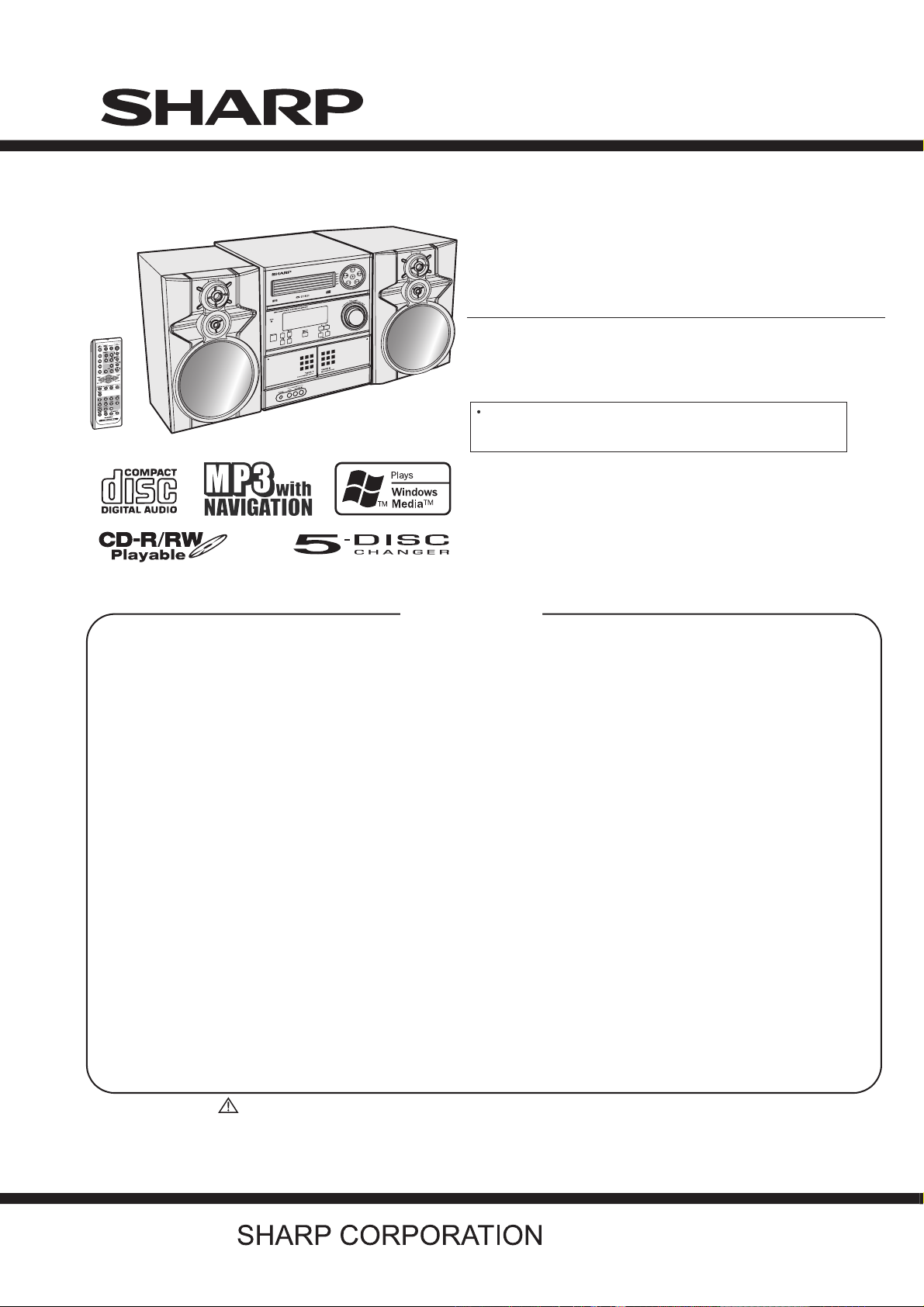
CD-MPX870W
In the interests of user-safety the set should be restored to its
origina
l condition and only parts identical to those specified be
used
.
SERVICE MANUAL
No. S6622CDMP870W
MINI COMPONENT SYSTEM
CONTENTS
CHAPTER 1. GENERAL DESCRIPTION
[1] Precaution for using lead-free solder ............ 1-1
[2] Safety precaution for service manual ........... 1-2
Voltage selection............................................1-2
[3]
AC power supply cord AC plug adaptor.........1-2
[4]
Specifications.................................................1-3
[5]
Names of parts...............................................1-4
[6]
CHAPTER 2. ADJUSTMENTS
Mechanism section ....................................... 2-1
[1]
Test mode ..................................................... 2-2
[2]
CD section ..................................................... 2-4
[3]
CD Changer mechanism section ................... 2-5
[4]
MODEL
CD-MPX870W Mini Component System consisting of
-MPX870W (main unit) and CP-MPX870 (speaker
CD
system
).
CH
APTER 5. CIRCUIT DESCRIPTION
Waveforms of CD circuit............................... 5-1
[1]
Voltage ......................................................... 5-2
[2]
APTER 6. CIRCUIT SCHEMATICS AND PARTS
CH
LAYOUT
Notes on schematic diagram........................ 6-1
[1]
Types of transistor and LED.......................... 6-1
[2]
Schematic diagram........................................ 6-2
[3]
Wiring side of PWB ......................................6-10
[4]
APTER 7. FLOWCHART
CH
Troubleshooting............................................ 7-1
[1]
CD-MPX870W
CHAPTER 3. MECHANISM BLOCKS
[1] Caution on disassembly................................. 3-1
Removing and reinstalling the main parts ...... 3-4
[2]
CHAPTER 4. DIAGRAMS
CD Block diagrams ....................................... 4-1
[1]
Main Block diagrams .................................... 4-2
[2]
Parts marked with " " are important for maintaining the safety of the set. Be sure to replace these parts with specified
ones for
maintaining the safety and performance of the set.
APTER 8. OTHERS
CH
Function table of IC ...................................... 8-1
[1]
FL Display .................................................... 8-8
[2]
rts Guide
Pa
This document has been published to be used
for
after sales service only.
The contents are subject to change without notice.
Page 2
CD-MPX870W
CHAPTER 1: GENERAL DESCRIPTION
[1] PRECAUTIONS FOR USING LEAD-FREE SOLDER
1. Employing lead-free solder
"MAIN, POWER, DISPLAY, GAME INPUT, CD SERVO, LED, CD MOTOR (PWB ONLY), CD CHANGER MOTOR
(PWB ONLY) PWB" of this model employs lead-free solder.The LF symbol indicates lead-free solder, and is
attached on
lead-free solder
Example:
2. Using lead-free wire solder
When fixing the PWB soldered with the lead-free solder, apply lead-free wire solder. Repairing with
conventional lead wire solder may cause damage or accident due to cracks
As the melting point of lead-free solder (Sn-Ag-Cu) is higher than the lead wire solder by 40 C, were
commend you to use a dedicated soldring bit,if you are not familiar with how to obtain lead-free wire solder or
soldering bit,contact our service station or service branch in your area.
3. Soldering
As the melting point of lead-free solder (Sn-Ag-Cu) is about 220 C which is higher than the conventional lead
solder by 40 C, and as it has poor solder wettability, you may be apt to keep the soldering bit in contact with the
PWB for extended period of time. However, since the land may be peeled off or the maximum heat-resistance
temperature of parts may be exceeded, remove the bit from the PWB as soon as you confirm the steady
soldering condition.
Lead-free solder contains more tin, and the end of the soldering bit may be easily corrected. Make sure to turn
on and off the power of the bit as required.
If a different type of solder stays on the tip of the soldering bit, it is alloyed with lead-free solder.Clean the bit
after every use of it
When the tip of the soldering bit is blackened during use, file it with steel wool or fine sandpaper.
Be careful when replacing parts with polarity indication on the PWB silk
Lead-free wire solder for servicin
the PWB and service manuals.The alphabetical character following LF shows the type of
.
Indicates lead-free solder of tin,silver and copper.
.
.
.
g
Ref No.
PWB-A 92LPWB6570MANS
PWB-B 92LPWB6570DPLS
C
PWB-
PWB-
D
Parts No.
92LPWB6514CDU
92LPWB6274LED
QPWBF0027AWZZPWB-E
QPWBF1055AWZZPWB-F
MAIN (A1), POWER (A2)
DISPLAY (B1), GAME INPUT (B2)
S
CD SERV
S
LE
CD MOTOR (PWB ONLY)
CD CHANGER MOTOR (PWB ONLY)
O
D
Description
1 – 1
– i –
Page 3
[2]
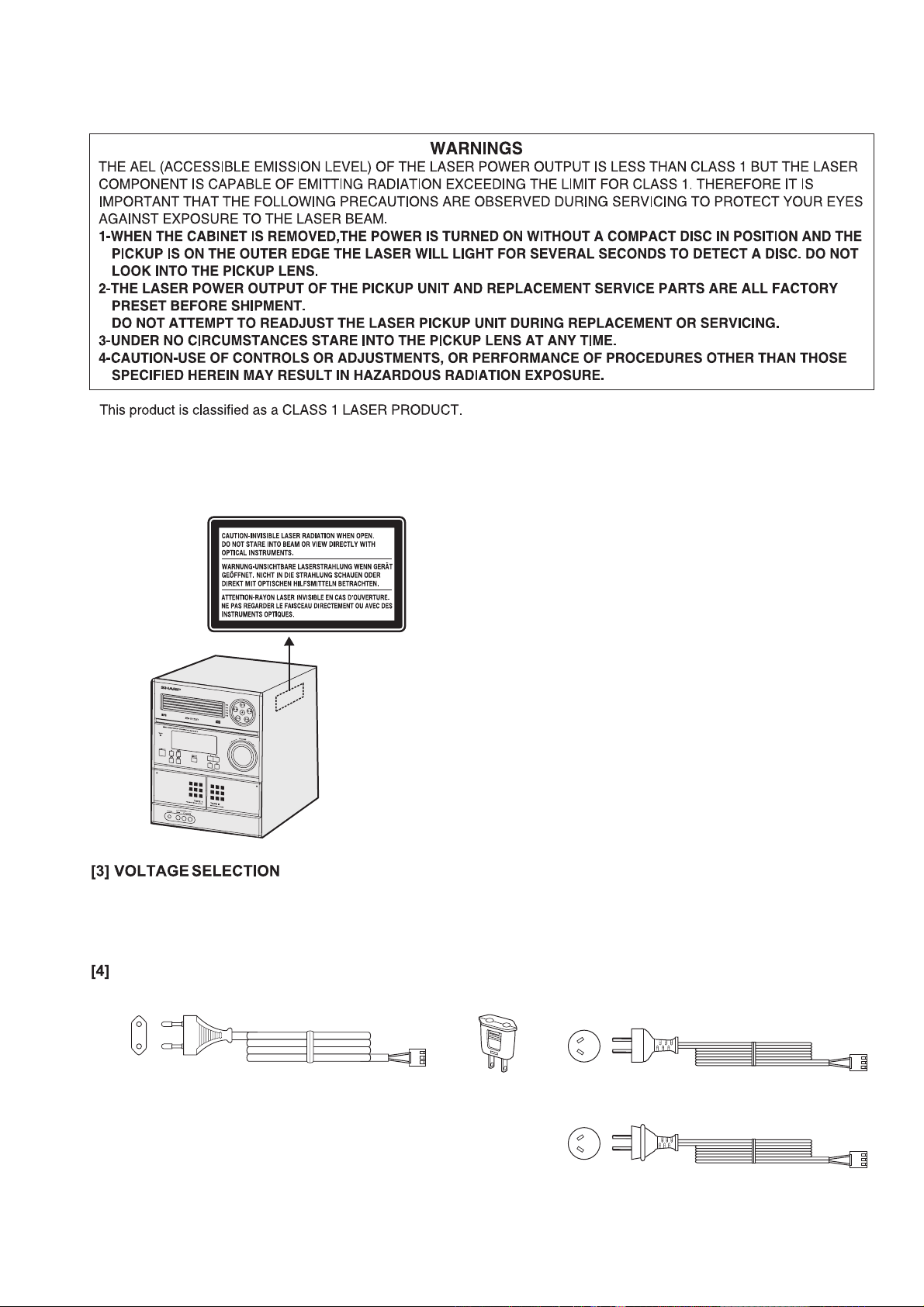
SAFETY PRECAUTION FOR SERVICE MANUAL
Precaution to be taken when replacing and servicing the Laser Pickup.
Laser Diode Properties
Material: GaAIAs
Wavelength: 795 nm
Emission Duration: continuous
Laser Output: max. 0.6 mW
Note for users in Australia:
Copyright
may exist in material you wish to record.
Copying or broadcasting such material without
pe
rmission of the relevant in licenses or owners of
the copyright is prohibited by law. SHARP is not in a
position to authorise the copying or broadcasting of
copyright
materials and nothing in this OPERATION
MANUAL should be implied as giving that authority.
CD-MPX870W
For other countries:
Audio-visual
which
owner
in your country
Before operating the unit on mains, check the preset voltage. If the voltage is different from your local
voltage, adjust the voltage as follows. Turn the selector with a screwdriver until the appropriate voltage
number appears in the window (110V, 127V, 220V or 230V - 240V AC).
material may consist of copyrighted works
must not be recorded without the authority of the
of the copyright. Please refer to the relevant laws
.
AC POWER SUPPLY CORD AND AC PLUG ADAPTOR
QACCEA001AW00
QPLGA0004AWZZ
QACCZ0013AW00
QACCL0008AW00
–2
1 – 2
Page 4
CD-MPX870W
[5]
SPECIFICATIONS
FOR A COMPLETE DESCRIPTION OF THE OPERATION OF THIS UNIT, PLEASE REFER
TO THE OPERATION MANUAL
.
As part of our policy of continuous improvement,
SHAR P
specifcation
without
figures
uni t s
rese r v es the r ight t o make d e s ign an d
changes for product improv e m e n t
prior notice. The performance specifcation
indicated are nominal values of production
.There m a y b e some deviations f r om these
values in individual units.
General
Power source
Power consumption
Dimensions Width: 10 - 1/4" (260 mm)
Weight
AC 110/127/220/230-240 V, 50/60Hz
120 W
Height: 13" (330 mm)
Depth: 12 - 7/8" (323 mm)
18.74 lbs. (8.5 kg)
Amplifier
Output power
Output terminals Speakers: 6 ohms
Input terminals Game/ Auxiliary (audio signal):
600 W (300 W + 300 W) (10% T.H.D.)
MPO:
RMS:
300 W (150 W + 150 W) (10% T.H.D.)
RMS:
240 W (120 W + 120 W) (0.9% T.H.D.)
Headphones: 16 - 50 ohms
(recommended: 32 ohms)
Video output: 1Vp-p
500 mV/ 47 k ohms
Game/Video: 1Vp-p
Tuner
Frequency range
FM: 88.0 - 108.0 MHz
AM: 531 - 1602 kHz
Cassette deck
Frequency
response
Signal/noise ratio 55 dB (TAPE 1, playback)
Wow and flutter 0.3 % (WRMS)
50 - 14,000 Hz (normal tape)
50 dB (TAPE 2, recording/playback)
Front Speaker
Type 3-way type speaker system
Super tweeter
2" (5 cm) tweeter
6 - 5/16" (16 cm) woofer
Maximum input
power
Rated input power 150 W
Impedance 6 ohms
Dimensions Width: 7 - 7/8" (200 mm)
Weight 7.3 lbs. (3.3 kg) /each
300 W
Height: 13" (330 mm)
Depth: 9 - 1/8" (231 mm)
CD player
Type 5-disc multi-play compact disc player
Signal readout Non-contact, 3-beam semiconductor laser
D/A converter 1-bit D/A converter
Frequency
response
Dynamic range 90 dB (1 kHz)
pickup
20 - 20,000 Hz
1 – 3
– 4
Page 5
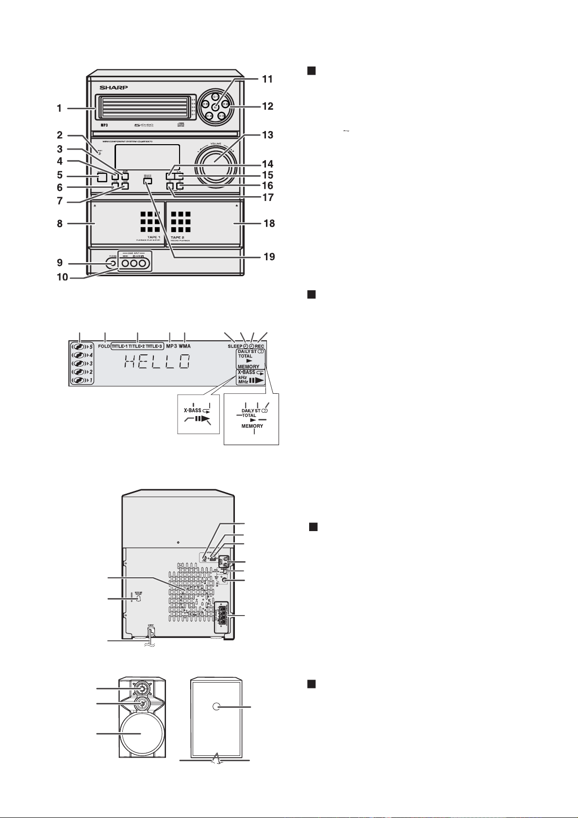
[6]
NAMES OF PARTS
1 2 3 4 5 6 7 8 9
16 17
18
19
10
11 1213
14
15
Front panel
1. Disc Trays
2. Timer Indicator
3. Tuner (Band) Button
4. CD Button
5. ON/STAND-BY Button
6. Tape (1 2) Button
7. Game/Video Button
8. Tape 1 Cassette Compartment
9. Headphone Jack
. Game/ Video Input Jac
10
11. Disc Tray Open/Close Button
. Disc Number Select Buttons
12
13. Volume Control
. CD or Tape Stop Button
14
. CD Play or Repeat,
15
16
. CD Track Up or Fast Forward, Tape 2 Fast Forward,
Tuner Preset Up, Time Up Button
. CD Track Down or F
17
Tuner Preset Down,
18
. Tape 2 Cassette Compartment
. Remote Sensor
19
ks
Tape Play Button
ast
Reverse, Tape 2 Rewind,
Time Down Button
Display
1. Disc Number Indicators
2. MP3/ WMA Folder Indicator
3. MP3/ WMA Title Indicators
4. MP3 Indicator
5. WMA Indicator
6. Sleep Indicator
7. Timer Play Indicator
8. Timer Recording Indicator
9. Tape 2 Record Indicator
10. MP3/WMA Total Indicator
11
. Daily Timer Indicator
12
. FM Stereo Mode Indicator
13
. FM Stereo Receiving Indicator
14
. Tape Play Indicator
15. Memory Indicator
16
. Extra Bass Indicator
17
. Disc Repeat Play Indicator
18
. Disc Pause Indicator
. Disc Play Indicator
19
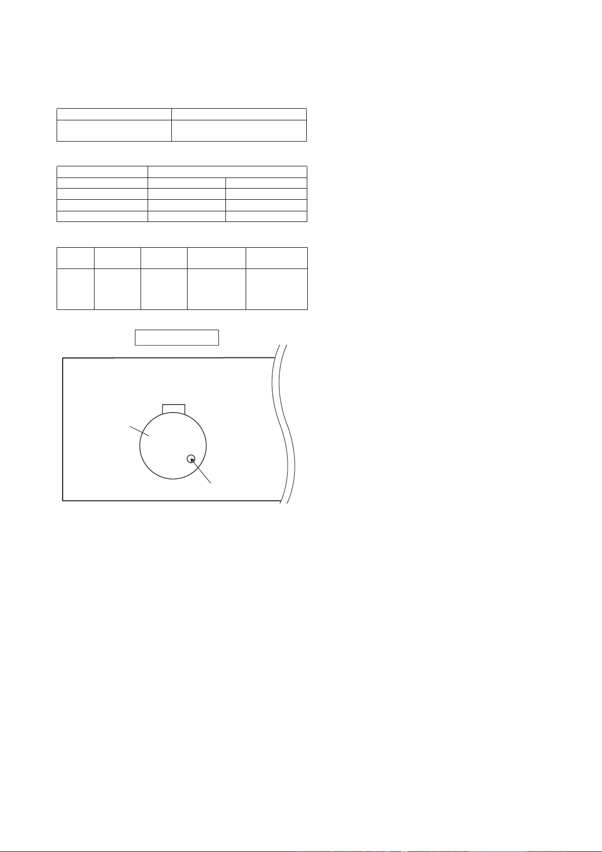
CD-MPX870W
4
5
6
7
1
8
9
2
10
Rear panel
1. Cooling Fan
2. AC Voltage Selector
3. AC Power Cord
4. FM 75 Ohms Antenna Jack
5. AM Antenna Ground Terminal
6. AM Loop Antenna Terminal
7. Speaker Light-up Jacks
8. Span Selector Switch
9. Video out Jack
10. Front Speaker Terminals
3
11
2
4
3
Front Speaker
Tweeter
2.1.Super Tweeter
3. Woofer
4. Bass Reflex Duct
5. Speaker Wire
6. Speaker Light-Up Wire
56
1 – 4
–2
Page 6

CD-MPX870W
1
Remote control
1. Remote Control Transmitter
13
7
14
8
15
9
2
10
16
11
22
17
18
19
20
21
23
3
24
4
25
26 27 28 29
5
6
12
2. Disc Number Select Buttons
3. Clock/Timer Button
4. Character Input/Disc Direct Search Buttons
5. Equalizer Mode Select Button
6. Extra Bass/Demo Button
7. ON/STAND-BY Button
8. CD Button
9. Tuner (Band) Button
10. Tape (1 2) Button
11. Game/Video Button
12. Volume Up and Down Buttons
13. Disc Clear/Dimmer Button
14. Disc Random Button
15. Disc Stop Button
16. Tape Stop Button
17. Memory Button
18. Disc Pause Button
19. Disc Play or Repeat Button
20. Tape Play Button
21. Tape 2 Record Pause Button
22. Tuning Up, Cursor Up Button
23. Disc Track Up or Fast Forward, Tape 2 Fast Forward,
Tuner Preset Up, Time Up, Cursor Right Button
24. Disc Track Down or Fast Reverse, Tape 2 Rewind,
Tuner Preset Down, Time Down, Cursor Left Button
25. Tuning Down, Cursor Down Button
26. MP3/WMA Navigation Mode Select Button
27. Character Button
28. MP3/WMA Display Button
29. Enter Button
1 – 5
– 4
Page 7
CD-ES700/CD-ES77CD-ES700/CD-ES77Service ManualCD-ES700/CD-ES77MarketE
CHAPTER 2. ADJUSTMENTS
[1] Mechanism section
• Driving Force Check
Torque Meter Specified Value
Play: TW-2111 Tape 1: Over 80 g
• Torque Check
Torque Meter Specified Value
Play: TW-2111 30 to 80 g.cm 30 to 80 g.cm
Fast forward: TW-2231 — 70 to 180 g.cm
• Tape Speed
Tape 2: Over 80 g
Tape 1 Tape 2
— 70 to 180 g.cm
CD-MPX870W
Test Tape Adjust-
Normal
speed
MTT-111 Variable
Tape
Motor
Figure 1
ing Point
Resistor in
motor.
TAPE MECHANISM
Variable Resistor in motor
Specified
Value
3,000 ± 30 Hz
Speaker
Instrument
Connection
Speaker Terminal (Load
resistance: 6
ohms)
2 – 1
Page 8
CD-MPX870W
[2] Test mode
• Setting the test mode
During stand-by mode, press GAME/VIDEO button
while pressing down the button and button.
then, press the CD button to enter the test mode.
C D T E S T
OPEN/CLOSE operation is using manual. IL isn’t done
<< >>,<< >>buttons make pick's slide possible.
to page 2-3
<<PLAY>> key input.
Do TOC IL. Do normal play.
When these following key is input into PLAY key, track number can be appoint directly.
<< 1>> key: Track 4
<< 2>> key: Track 9
<< 3>> key: Track 15
A
IL isn’t done
IL isn’t done
<<MEMORY>>
key input.
Adjustment result automatically will
display as below for each 2 sec:
a) "FOF_XXXX"
b) "TOF_XXXX"
c) "TBAL_XX"
d) "TGAN_XX"
f) "FGAN_XX"
g) "RFLS_XX"
<<STOP>> key input.
STOP
explanation:
a) Focus off set = "FOF_XXXX"
b)Tracking off set = "TOF_XXXX"
c)Tracking balance = "TBAL_XX"
d)Tracking Gain = "TGAN_XX"
f) Focus Gain = "FGAN_XX"
g) RF level shift = "RFLS_XX"
VOL — Last memory
P.GEQ — FLAT
X-BASS — OFF
To cancel : Power OFF
––––––––
2 – 2
Page 9
A
<<MEMORY>> key input.
Laser ON.
<<MEMORY>> key input.
Tracking OFF play at that specific point.
<<MEMORY>> key input.
Tracking ON play from that specific point.
CD-MPX870W
<<MEMORY>> key input.
Adjustment result automatically will display as below for each 2 sec :
a) "FOF_XXXX"
b) "TOF_XXXX"
c) "TBAL_XX"
d) "TGAN_XX"
f) "FGAN_XX"
g) "RFLS_XX"
<<STOP>> key input.
STOP
Sliding the PICKUP with<< >>, << >> button
must only be in STOP mode.
explanation:
a) Focus off set = "FOF_XXXX"
b)Tracking off set = "TOF_XXXX"
c)Tracking balance = "TBAL_XX"
d)Tracking Gain = "TGAN_XX"
f) Focus Gain = "FGAN_XX"
g) RF level shift = "RFLS_XX"
VOL — Last memory
P.GEQ — FLAT
X-BASS — OFF
To cancel : Power OFF
2 – 3
Page 10
CD-MPX870W
[3] CD section
CD Error code description
Error Explanation
10* CAM error. Can't detect CAM switch when CAM is moving.
11* When it detect cam operation error during initialize
process.
20* TRAY error. Can't detect TRAY switch when TRAY is
moving.
21* When it detect TRAY operation error during initialize
process.
31 When it change to CD function, DSP cannot read initial
data.
* 'CHECKING'
If Error is detected, 'CHECKING' will be displayed instead of 'ER-CD**'. 'ER-CD**' display will only be displayed
when error had been detected for the 5
Standard Specification of Stereo System Error Message Display Contents
Error Contents Display Notes
CD CD Changer Mechanism Error. 'ER-CD**' (*) 10: CAM SW Detection NG during normal operation.
CD DSP Communication Error. 'ER-CD31' DSP COMMUNICATION ERROR.
Focus Not Match/IL Time Over. 'NO DISC'
TUNER PLL Unlock. PLL Unlock.
th
times.
FM 87.5 MHz
11: CAM SW Detection NG during initialize process.
20:TRAY SW Detection NG during normal operation.
21:TRAY SW Detection NG during initialize process.
(*) CHECKING:
If CD changer mechanism error is detected, 'CHECKING' will be display instead of 'ER-CD**'. 'ER-CD**' display will
only be display when error had been detected for the 5
th
times.
Speaker abnormal detection and +B PROTECTION display
In case speaker abnormal detection or +B PROTECTION had occurred, the unit will automatically enter to stand - by
mode and Timer indicator will be flashing as below.
Example : In case of speaker abnormal
TIMER
LED
ON
OFF
NO. 1
NO.1 : +B Protection
NO.2 : Speaker abnormal
OFF
FLASHING
NO. 2
1 FRAME
OFF
ON
NO. 1
FLASHING
OFF
NO. 2
(REPEAT)
+B PROTECTION is condition when irregular process occur on power supply line.
BEFORE TRANSPORTING THE UNIT
The following process need to be taken after set tapering/parts replacement.
1. Press the ON/STAND-BY button to enter stand-by mode.
2. While pressing down the button and the button, press the GAME/VIDEO button. The Micro Computer
version number will be displayed as "CM*****".
3. Press button until "WAIT"→ "FINISHED" appears.
4. Unplug the AC cord and the unit is ready for transporting.
2 – 4
Page 11
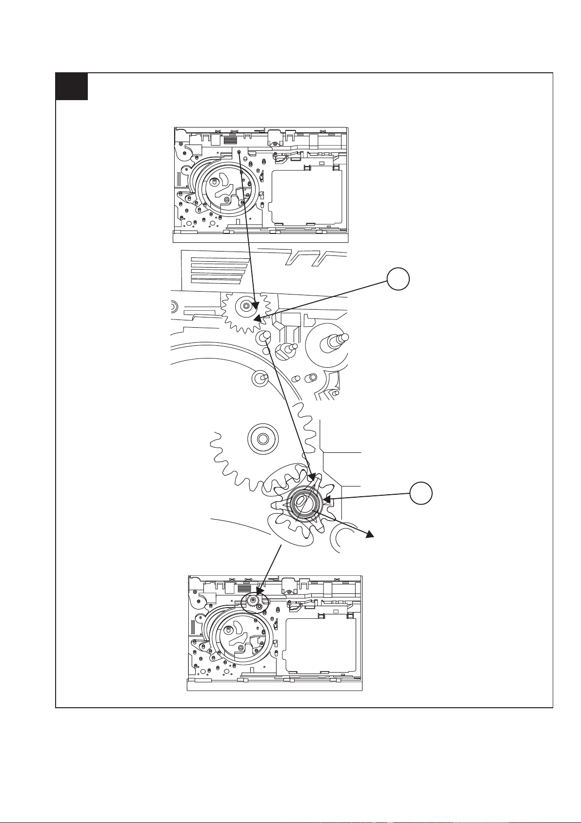
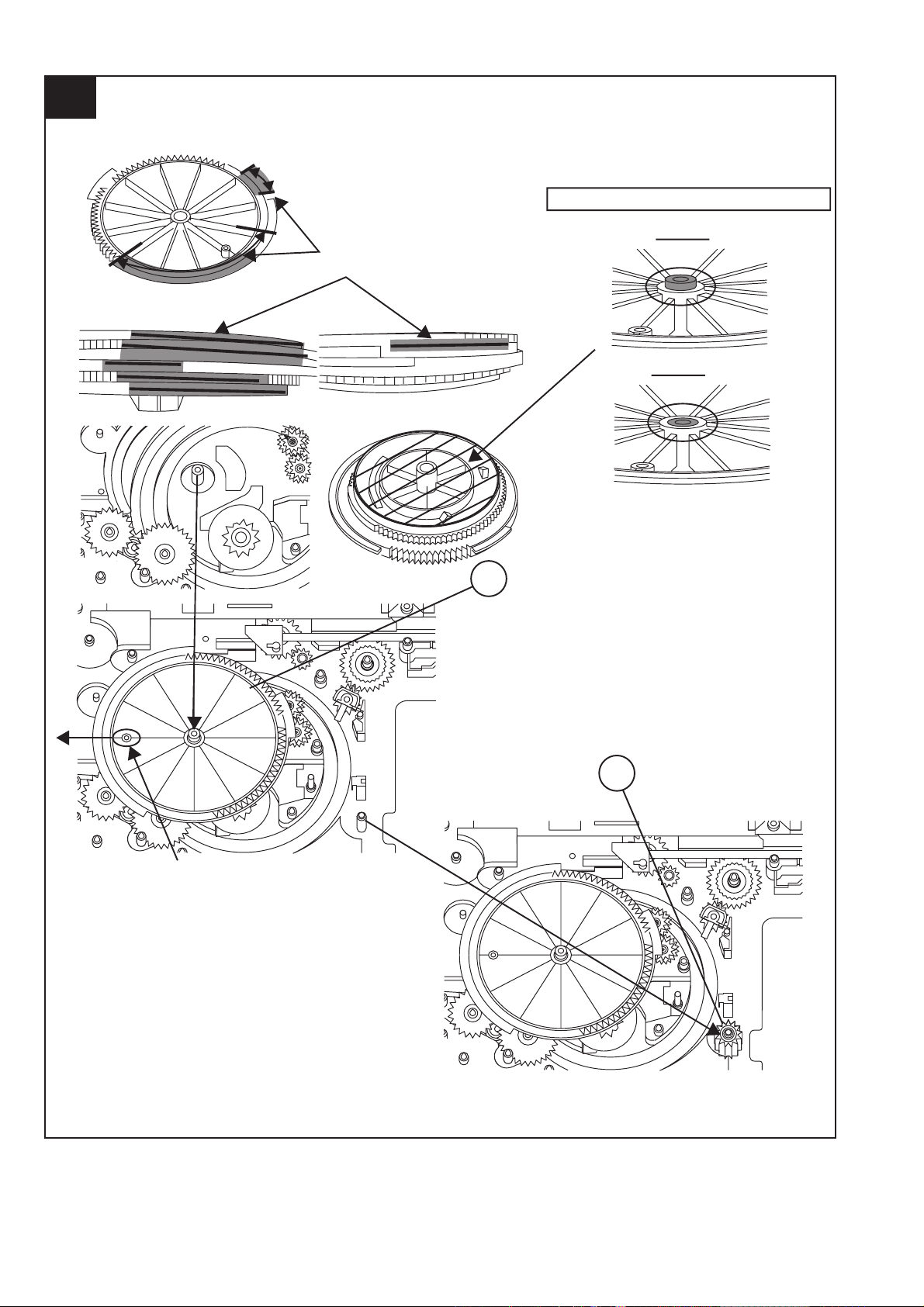
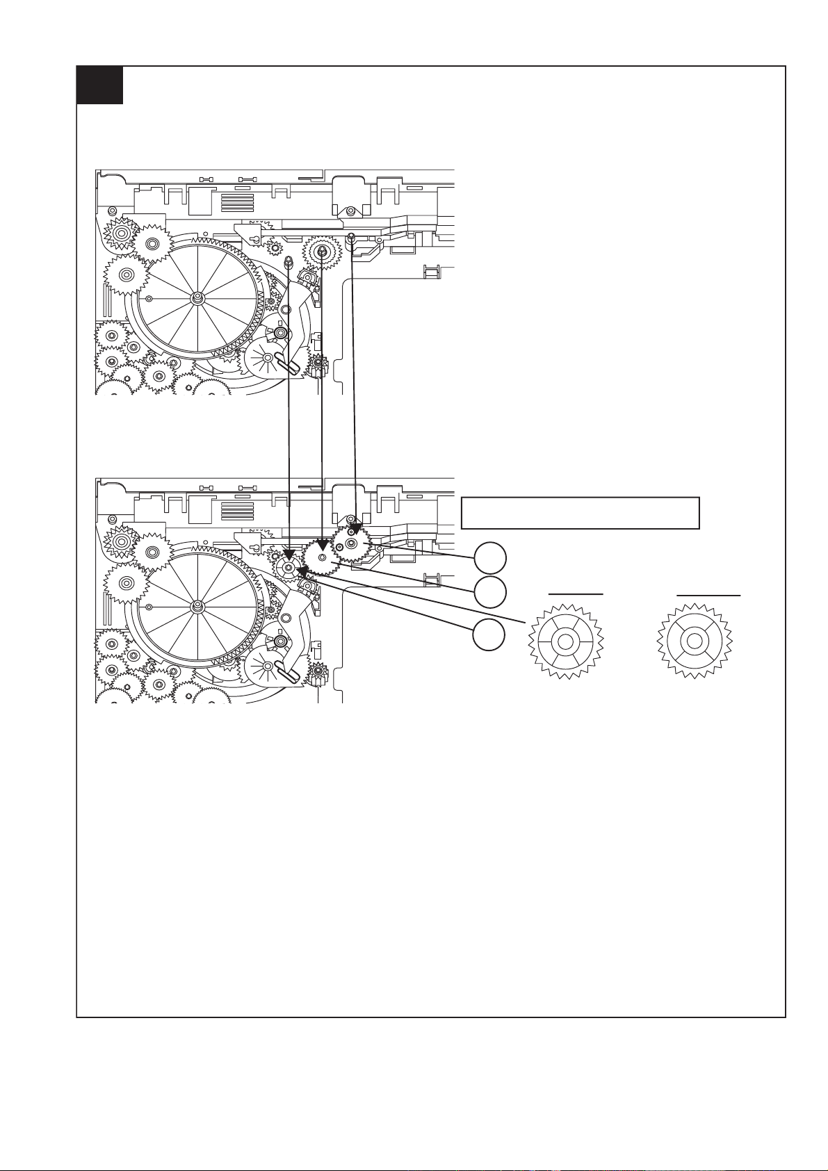
[4] CD Changer mechanism section
• All numbers in the drawing correspond to those in parts guide (CHANGER MECHANISM PARTS).
1
141
CD-MPX870W
140
HALF GEAR
MUST BE ARRANGED AS SHOWN
2 – 5
Page 12
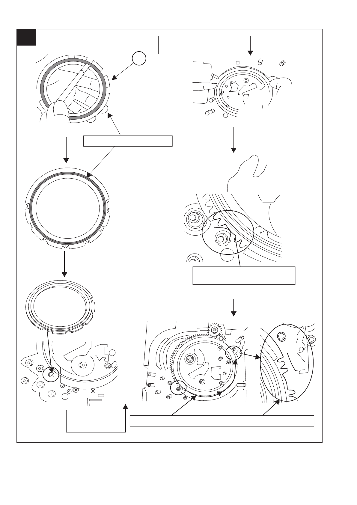
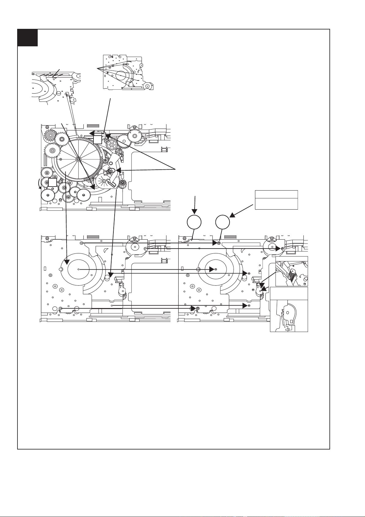
CD-MPX870W
2
139
APPLY SANKOL SHS1001 BEFORE FIX
FIX ITEM 139 ACCORDING TO THE
PICTURE AS SHOWN ABOVE
ROTATE MODE BIG GEAR UNTIL REACH AS SHOWN IN PICTURE
2 – 6
Page 13
3
CD-MPX870W
143
APPLY GREASE SC141
112
PULL THE LEVER UNITIL
REACH THE ARROW MARK
2 – 7
Page 14
CD-MPX870W
4
FIGURE 2
FIGURE 1
152
142
APPLY GREASE SC141
118
SLOT CLAMP
SWITCH ARM INSIDE BASE SLOT
HALF GEAR MUST BE
ARRANGED AS SHOWN
2 – 8
Page 15
5
CD-MPX870W
APPLY GREASE SC141 AT BOTTOM SIDE
OF GEAR FOLLOW MARKING (REFER TO GRAY AREA)
NO NEED TO APPLY GREASE AT BOTTOM
SIDE
FIGURE 1
APPLY GREASE SC141
AT TOP SIDE OF GEAR
FOLLOW MARKING
(REFER TO GRAY AREA)
127
IF DIRECTION IS OTHER THAN DIRECTION
SHOWN IN FIGURE 1, IT IS INCORRECT
CORRECT
128
INCORRECT
BLACK MARK
2 – 9
Page 16
CD-MPX870W
6
APPLY GREASE SC141 AT
HALF GEAR AREA
ROTATE CLOCKWISE UNTIL REACH HERE (MAXIMUM)
129
2 – 10
Page 17
7
CD-MPX870W
151150149
2 – 11
Page 18
CD-MPX870W
8
THE SHOWN AREA MUST FREE FROM GREASE
CORRECT
GREASE SC141 APPLICATION LENGTH
GREASE APPLICATION PORTION
INCORRECT
SHOWN HOLE MUST FACING ARROW DIRECTION
124
131
2 – 12
Page 19
9
138 126 125
CD-MPX870W
APPLY GREASE SC141
AT BOTTOM SIDE
ONLY
TR-RE JOINT GEAR C
APPLY GREASE SC141 ONLY AT TOP SIDE GEAR
MUST BE FIXED ACCORDINGLY TO
THE HOLE'S
2 – 13
Page 20

CD-MPX870W
10
148 147 146 145
2 – 14
Page 21
11
CD-MPX870W
121
144
WHEN FIXING ITEM 144 MUST FOLLOW AS SHOWN
APPLY GREASE SC141
130
2 – 15
Page 22
CD-MPX870W
12
117
FIGURE 2
FIGURE 1
APPLY GREASE
SC141
FIGURE 3
APPLY GREASE SC141
2 – 16
Page 23
13
CD-MPX870W
ITEM 133 , 134 MUST APPLY GREASE SC141
ON TOP SIDE GEAR ONLY
134
GEAR 112 GEAR 112
133
132
CORRECT
TOP VIEW AFTER
BEING ASSEMBLED
INCORRECT
IT IS INCORRECT TO
FIX IT IN REVERSED
DIRECTION
2 – 17
Page 24
CD-MPX870W
14
APPLY GREASE SC141
BEFORE FIX
A
MOVE 112 UNTIL TOUCH THE WALL
B
DURING GEAR A ROTATE
MUST PRESS SHOWN AREA
AND LEVER B WILL MOVE
ARROW DIRECTION THEN
FIX PART 108
SCREW TORQUE
+0.5
2 kgf-cm
- 0
108 803 x6
APPLY GREASE SC141
CONFIRM WHETHER
FIXED
PROPELY OR NOT
2 – 18
Page 25
15
CD-MPX870W
APPLY GREASE SC141
113
BEHIND THE LEVER NEED TO APPLY GREASE SC141
PULL IT THEN LEVER WILL
MOVE IN
2 – 19
Page 26
CD-MPX870W
16
123
115
APPLY GREASE SC141
APPLY GREASE SC141 BEFORE FIX
APPLY GREASE
SC141 AT BOSS
SPRING MUST BE ARRANGED UNDER THE HOOK
CORRECT LR JOINT LEV
BOARD R
BOARD R
LR JOINT LEV
INCORRECT
2 – 20
Page 27
17
CD-MPX870W
IT IS INCORRECT IF ASSEMBLED IN
A REVERSED DIRECTION
103 137 136
APPLY GREASE SC141
BIG SLOT MUST FACING OUT
WHEN FIX AND AFTER FIXED TO BASE CHASSIS.
AFTER ASSEMBLY, CONFIRM WITH FREE DROP TEST
GEAR POSITION DURING FIXING
2 – 21
Page 28

CD-MPX870W
18
IT IS INCORRECT IF ASSEMBLED IN
A REVERSED DIRECTION
APPLY GREASE SC141
104
135
136
BIG SLOT MUST FACING OUT
WHEN FIX AND AFTER FIXED TO BASE CHASSIS
AFTER ASSEMBLY, CONFIRM WITH FREE DROP TEST
GEAR POSITION DURING FIXING
CONFIRM BOTH GEARS SIT PROPERLY AND LOCKED
2 – 22
Page 29
19
120
CD-MPX870W
AFTER FIX OUTER UP/DOWN LEVER HOLD AS SHOWN PORTION AND
MOVE UP/DOWN THEN CONFIRM WHETHER LEVER GO INSIDE THE HOLE OR NOT
137
IT IS CORRECT IF THE LEVER HOLD
BIGGER SLOT FACING OUT
ENTERS THE HOLE
119
IT IS INCORRECT IF THE LEVER HOLD DOES NOT
ENTER THE HOLE
135
BIGGER SLOT FACING OUT
ALL OF THIS 135 AND 137 GEAR FIX TOGETHER WITH 119
AND 120 LEVER ( MOVE TOGETHER )
2 – 23
Page 30
CD-MPX870W
20
BIG SLOT FACING OUT
110
2 – 24
Page 31

21
CD-MPX870W
PUSH THE LEVER ACCORDING TO ARROW
DIRECTION THEN FIX
WHEN FIXING MAIN BASE ASSEMBLY FOLLOW ACCORDING TO PICTURE 1
PICTURE 1
CORRECT INCORRECT INCORRECT
MAKE SURE MECHA HOLDER SHAFT FIX PROPERLY TO LEVER
PICTURE 3
PICTURE 2
2 – 25
Page 32

CD-MPX870W
22
APPLY SANKOL (SHS1001)
101
102
APPLY SANKOL
(SHS1001) ON TOP
APPLY SANKOL (SHS1001) INSIDE
THE SLOT & OTHER SHOWN PORTION
APPLY SANKOL
(SHS1001)
APPLY SANKOL (SHS1001) AT
TRAY SLIDING PORTION
FIX TRAY NO 1 FIRST THAN
FOLLOW OTHER
APPLY SANKOL (SHS1001) AT BACK PORTION
COSMO GUIDE TRAY HAVE
MARKING AS SHOWN
2 – 26
Page 33

23
GEAR UP/DOWN BOARD
111
APPLY GREASE SC141 AT INNER & OUTER GEAR SLIDING PORTION
WHEN FIX GEAR UP/
DOWN BOARD THE
TWO LEVER MUST AT
PARALLEL LINE AND
POSITIONED AT TOP
MAX SIDE
CD-MPX870W
2 – 27
AFTER ASSEMBLY GEAR UP/DOWN BOARD
Page 34

CD-MPX870W
24
SCREW TORQUE
+0.5
3 kgf-cm
- 0
ROTATE THE GEAR TO MOVE UP 111 GEAR
UP AND DOWN BOARD BEFORE SCREW
804
2 – 28
Page 35

25
CD-MPX870W
AFTER ASSEMBLY TOP PLATE
FIX THE FFC
FFC4
AFTER PUSH, MAKE SURE SNAP PROPERLY
PRESS IN
AFTER FIX, PUSH FOLLOW ARROW DIRECTION
BEFORE LOCK
AFTER LOCK
BACK
PORTION
107
122
BEFORE LOCK
SLOT IN
BEFORE LOCK
AFTER LOCK
AFTER LOCK
MUST CONFIRM
MUST CONFIRM
2 – 29
Page 36

CD-MPX870W
26
CORRECT
INCORRECT
CAUTION
1. MAKE SURE NO PWB CHIP INSIDE SET .( BEFORE FIX MAKE
SURE PWB IS FREE FROM DUST , GREASE & ETC )
803
2 – 30
Page 37

27
APPLY GREASE SC141
THE TWO SLOT MUST FREE
FROM GREASE SC141
APPLY GREASE SC141
BELOW THE MARKING
FOR BOTH PORTION
CD-MPX870W
ASSEMBLY SEQUENCE
1. APPLY GREASE SC141 TO MAIN BASE
GREASE SC141 APPLICATION AREA
ALL BOSS
APPLY GREASE
SC141
CAUTION
TRAY SLIDING
AREA MUST
FREE FROM
GREASE SC141
APPLY GREASE
SC141
APPLY GREASE
APPLY GREASE SC141 AT WALL
APPLY GREASE
SC141
SC141
105
APPLY GREASE SC141
AT BOTH SLOT
APPLY GREASE SC141 AT 3 HALF MOON
1 RIB ONLY
APPLY GREASE
SC141
APPLY GREASE SC141
INSIDE SLOT
2 – 31
Page 38

CD-MPX870W
28
REFERENCE ONLY
MOTOR GEAR HEIGHT FROM
MAIN BASE 12.2
+
0.1
-
0.1
-
+
12.2
MOTOR SCREWING HOLE
MUST HAVE GAP
M1,2
801
-0
13.8 + 0.2
APPLY GREASE SC141
SCREW TORQUE
1.5 + 0.5
-0
AFTER SCREW MOTOR, CONFIRM THE
ARRANGEMENT AS IN FIGURE 2
FIGURE 2
2 – 32
Page 39

29
APPLY SANKOL (SHS1001)
CD-MPX870W
3.1 + 0.1
SHAFT X 3 DIM AFTER INSERTION
MUST CONFIRM EVERYDAY
109-2
APPLY GREASE AT THE SLIDING PORTION
114
116
UP / DOWN
HOLDER CHANGE
TO NATURE
COLOR
SANKOL
APPLICATION AREA
(SHS1001)
APPLY GREASE SC141
2 – 33
Page 40

CD-MPX870W
30
BEFORE MELT IT
AFTER MELT IT ( MUST FLAT )
WHEN FITTING STABILIZER PLATE TO STABILIZER,
ROTATE STABILIZER ANTI CLOCKWISE BY JIG
( STRICTLY CANNOT FIT USING HAND)
( BY HAND CANNOT X )
BELOW
AFTER ASSEMBLED TO
HOLDER, STABILIZER
NEED TO BE CLEANED
WITH ALCOHOL DISC
TOUCHING SURFACE
2 – 34
Page 41

31
CD-MPX870W
106
APPLY GREASE SC141
MUST MAKE SURE SNAP PROPERLY BOTH SIDE
ALL SURFACE MUST TOUCH
CORRECT INCORRECT
GAP
INCORRECT
2 – 35
Page 42

CD-MPX870W
32
NO GAP HAVE GAP
CORRECT INCORRECT
2 – 36
Page 43

CD-MPX870W
CD-ES700/CD-ES77CD-ES700/CD-ES77Service ManualCD-ES700/CD-ES77MarketE
CHAPTER 3. MECHANISM BLOCKS
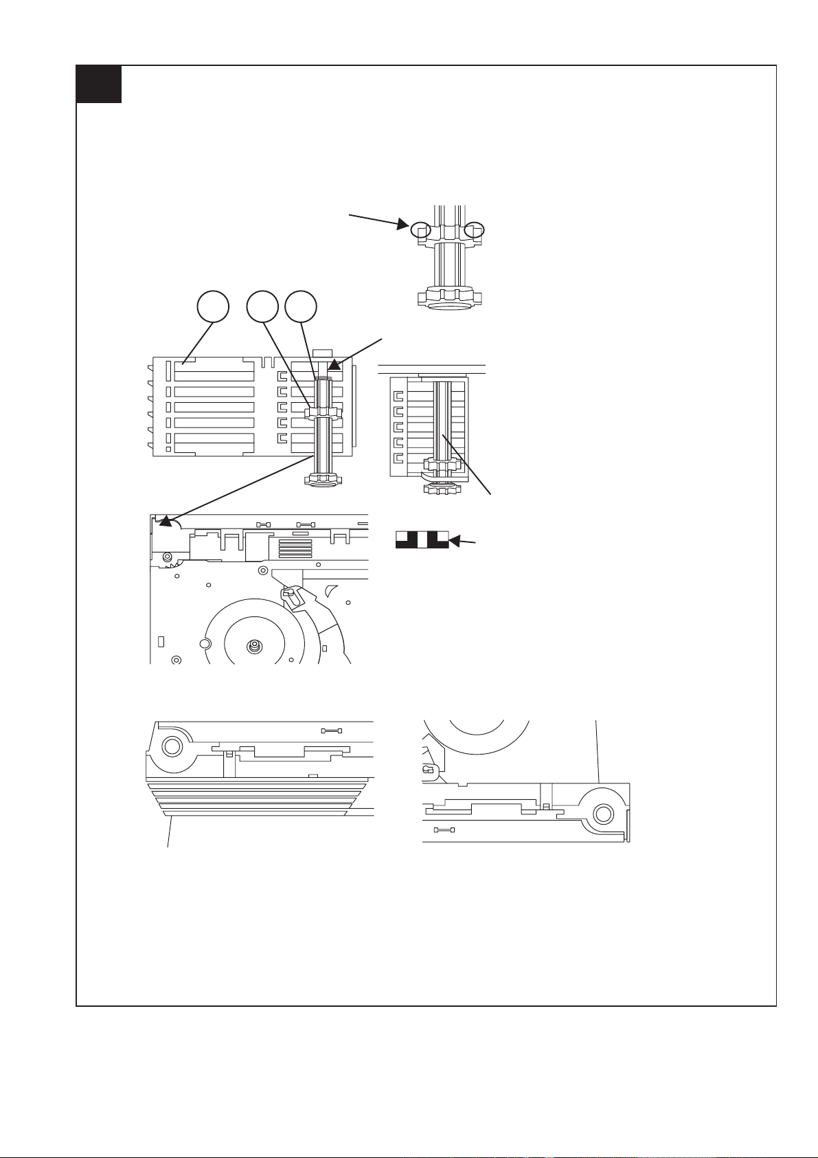
[1] Caution on disassembly
tion on Disassembly
Cau
Follow the below-mentioned notes when disassembling the unit and reassembling it, to keep it safe and ensure
excellent performance:
1. Take cassette tape and compact disc out of the unit.
2. Be sure to remove the power supply plug from the wall outlet before starting to disassemble the unit.
3. Take off nylon bands or wire holders where they need to be removed when disassembling the unit. After servicing
the unit, be sure to rearrange the leads where they were before disassembling.
STEP REMOVAL PROCEDURE FIGURE
1 Top Cabinet 1. Screw....................(A1) x5 1
2 Side Panel (Left/
Right)
2. Screw.....................(B1) x
8 1
3 CD Changer unit 1. Hook.......................(C1) x2
2. Socket....................(C2) x1
3. Flat Cable...............(C3) x1
4 Rear Panel with
1. Screw.....................(D1) x9 2
Fan motor
5 Front Panel 1. Screw.....................(E1) x3
2. Flat Cable...............(E2) x
2,3
1
3. Socket.....................(E3) x1
4. Hook.......................(E4) x
2
6 Main PWB 1. Screw......................(F1) x3
2. Socket.....................(F2) x4
7 Power PWB 1. Screw.....................(G1) x4 3
8 Tape Mechanism 1. Screw.....................(H1) x6 4
2. Flat Cable...............(H2) x1
9 Game Input PWB 1. Screw......................(J1) x2 5
10 Display PWB 1. Knob.......................(K1) x1
2.
Nut..........................(K2) x1
3.
Washer...................(K3) x1
Screw......................(K4) x6
4.
11 CD Servo PWB 1. Screw.....................(L1) x3 6
2. Flat Cable...............(L2) x2
2. Socket.....................(L3) x1
12 Changer
Mechanism Uni
1. Screw....................(M1) x
2. Changer Chassis...(M2) x
t
4
1
15 CD Mechanism 1. Screw.....................(N1) x4 8
Note:
removing the connector for the optical pickup from the
After
connector,
of
the connector so as to protect the optical pickup from electro-
static
wrap the conductive aluminium foil around the front end
damage.
Top Cabinet
Front Panel
2
2
2
3
2,3
3
5
7
CD Changer Unit
Rear Panel
(D1)x9
3x10mm
O
CD Servo PWB
PULL
Hook
(C1)x1
(E3)x1
Power PWB
Fan Motor
Figure 2
(F2)x1
(C3)x1
(F3)x1
(F2)x2
(C2)x1
Front Panel
Main PWB
(F1)x1
3x10mm
O
(E2)x1
(C1)x1
PULL
Lug wire
(E1)x1
3x10mm
O
Front Panel
Hook
(B1)x2
3x10mm
O
(A1)x1
3x12mm
O
(A1)x2
3x12mm
O
Side Panel
(Right)
(B1)x2
3x10mm
O
Figure 1
Rear Panel
O
(B1)x2
3x10mm
(B1)x2
3x10mm
O
O
Side Panel
(Left)
3 – 1
(A1)x2
3x12mm
Power
PWB
(E4)x1
PULL
(G1)x4
4x8mm
O
Figure 3
(F2)x1
(F1)x2
3x6mm
O
(E1)x2
3x8mm
O
Hook
(E4)x1
PULL
Page 44

CD-MPX870W
Mechanism
(H1)x6
3x10mm
O
Figure 4
Tape
(H2)x1
Front Panel
Lug wire
(M1)x4
3x10mm
O
(M2)x1
(K4)x6
O
2.6x10mm
Figure 5
(L2)x1
(J1)x2
Special
(L1)x3
3x10mm
O
(L3)x1
Front Panel
Display
PWB
Nut (K2)x1
(K1)x1
Washer
(K3)x1
Game Input PWB
(L2)x1
(N1)x4
2.6x10mm
O
CD Mechanism
Figure 7
Figure 8
Changer
Mechanism
Unit
Changer
Mechanism
Unit
Figure 6
CD Servo
PWB
Changer
Mechanism
Unit
3 – 2
Page 45

STEP REMOVAL PROCEDURE FIGURE
1 Woofer 1. Front Panel............(A1) x1 9
2. Socket....................(A2) x1
3. Screw.....................(A3) x2
4. Screw.....................(A4) x4
2 Tweeter 1. Screw.....................(B1) x2
3 Super tweeter
1. Screw.....................(C1) x2
CD-MPX870W
Speaker Box
Front Panel
(A1)x1
(A2)x1
LED PWB
(A3)x2
3x10mm
O
(B1)x2
3x10mm
O
WOOFER
(C1)x2
3x10mm
O
O
TWEETER
SUPER TWEETER
(A4)x4
4x16mm
Screwdriver
Figure 9
3 – 3
Page 46

CD-MPX870W
r
[2] Removing and reinstalling the main parts
1. TAPE MECHANISM SECTION
Perform steps 1 to 5 and 6 of the disassembly method
to remove the tape mechanism.
1.1. How to remove the record/playback and erase
heads (TAPE 2) (See Fig. 1)
1. When you remove the screws (A1) x 2 pcs., the
recording/playback head and three-dimensional
head of the erasing head can be removed.
TAPE 2
Clutch Ass'y
Pinch Roller
(C1)x1
Pull
<B>
Figure 3
<A>
Pinch
Rolle
Pawl
Record/Playback
Head
Erase Head
(A1)x2
φ
2x9mm
Figure 1
1.2. How to remove the playback head (TAPE 1)(See Fig. 2)
1. When you remove the screws (B1) x 2 pcs., the
playback head can be removed.
TAPE 1
Clutch Ass'y
Playback
Head
1.4. How to remove the belt (TAPE 2) (See Fig. 4)
1. Remove the main belt (D1) x 1 pc., from the motor
side.
2. Remove the FF/REW belt (D2) x 1 pc.
1.5. How to remove the belt (TAPE 1) (See Fig. 4)
1. Remove the main belt (E1) x 1 pc., from the motor side.
2. Remove the FF/REW belt (E2) x 1 pc.
Tape
TAPE 2
FF/REW
Belt
(D2)x1
Main Belt
(D1)x1
Main Belt
(E1)x1
Tape
Motor
TAPE 2
Main Belt
(D1)x1
Motor
TAPE 1
FF/REW
Belt
(E2)x1
TAPE 1
Main Belt
(E1)x1
Figure 4
1.6. How to remove the motor (See Fig. 5)
1. Remove the screws (F1) x 2 pcs., to remove the motor.
Tape
Motor
(B1)x2
φ
2x9mm
Figure 2
1.3. How to remove the pinch roller (TAPE 1/2) (See Fig. 3)
1. Carefully bend the pinch roller pawl in the direction
of the arrow <A>, and remove the pinch roller (C1) x
1 pc., in the direction of the arrow <B>.
Note:
When installing the pinch roller, pay attention to the
spring mounting position.
Clutch Ass'y
(F1)x2
φ2.6x5mm
Figure 5
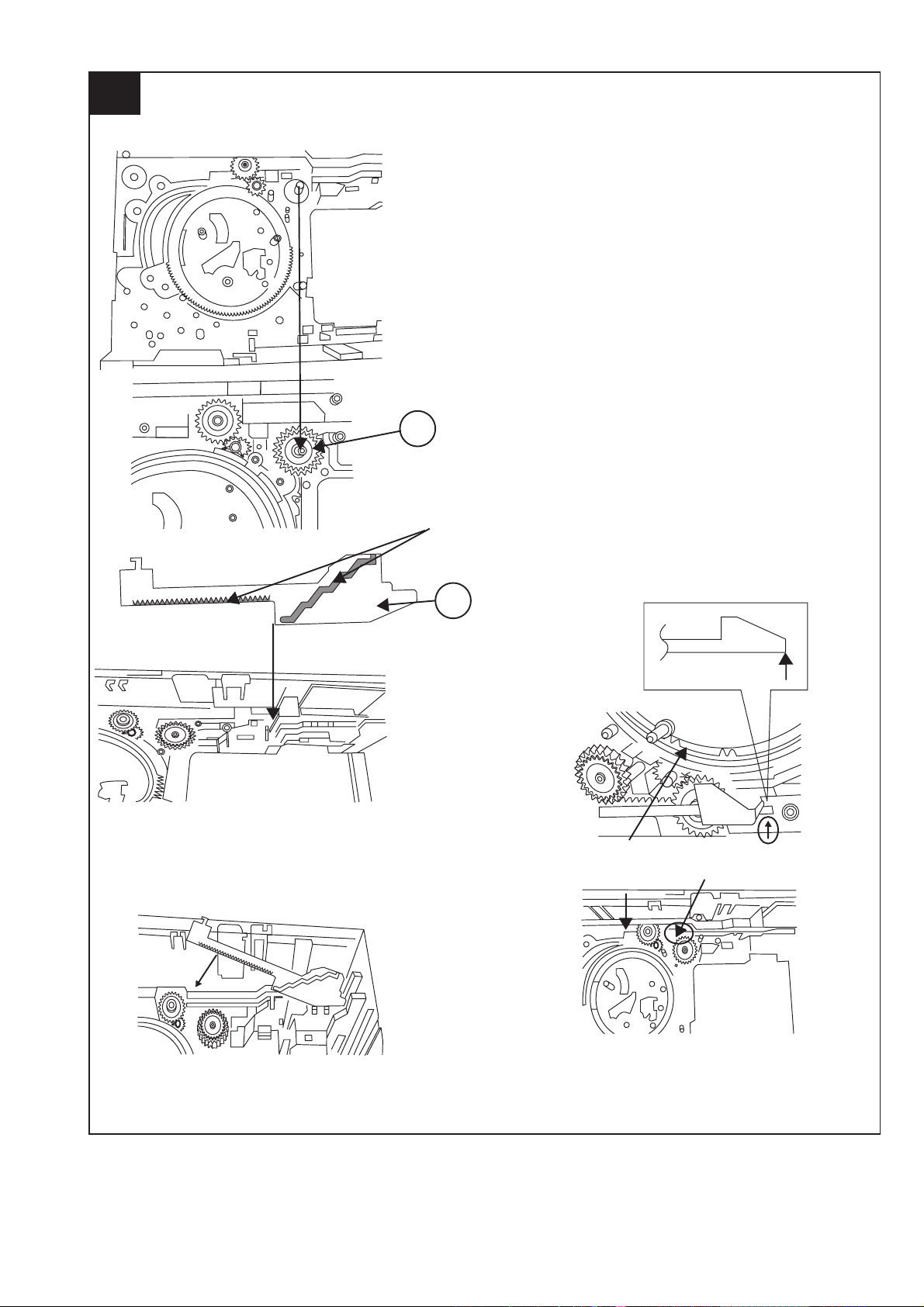
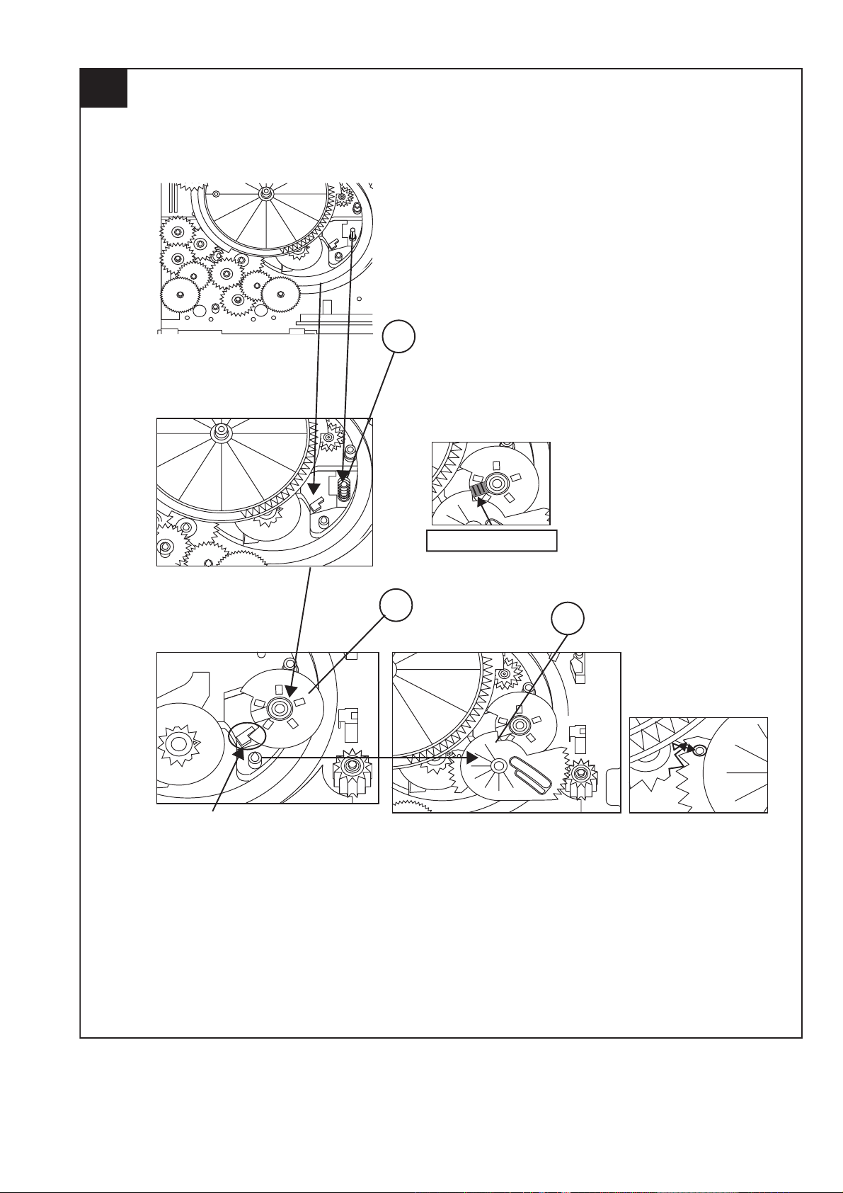
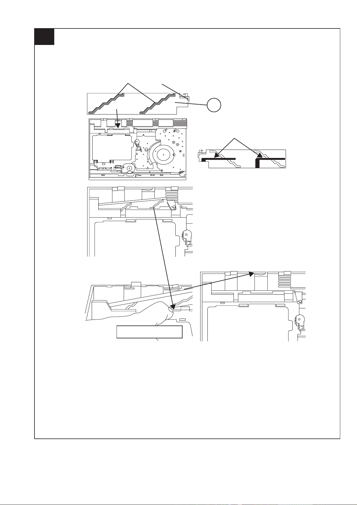
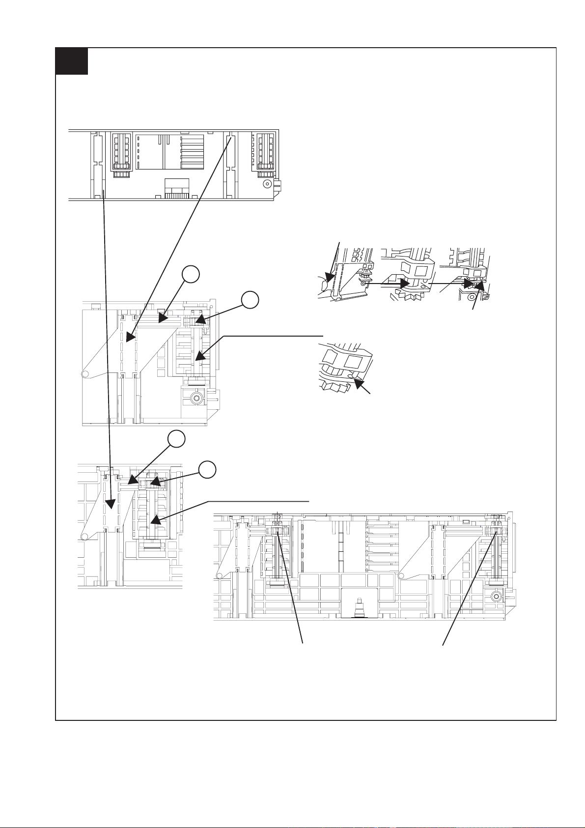
2. CD MECHANISM SECTION
Perform steps 1, 2, 9, 10, 11 and 12 of the disassembly method to remove the CD mechanism.
3 – 4
Page 47

2.1. Remove the pickup. (See Fig. 1)
Remove the stop washer (A1) x 1 pc., to remove the
1.
gear (A2) x 1 pc.
2. Remove the screws (A3) x 2 pcs., to remove the
shaft (A4) x 1 pc.
3. Remove the pickup.
Note:
After removing the connector for the optical pickup
from the connector wrap the conductive aluminium foil
around the front end of connector so as to protect the
optical pickup from electrostatic damage.
(A3)x2
φ2.6x6mm
CD Mechanism
Shaft
(A4)x1
Gear
(A2)x1
Stop Washer
(A1)x1
CD-MPX870W
Reduction gear C
Front Rear
Figure 3
2. In another case, if CD mechanism is at tray No.1
play position and to remove CD located in tray No.3,
the procedure is as follows:
If the gear up down board is located at tray No.1
position, then rotate gear clock-wise until it at stock
position. Rotate reduction gear D clockwis e (Figure
4) to move the CD mechanism to tray No.3 position.This is confirmed by checking the gear up down
board position by the marking as indicated on the
main chassis as shown in Figure 5.
Reduction gear D
Pickup Unit
Figure 1
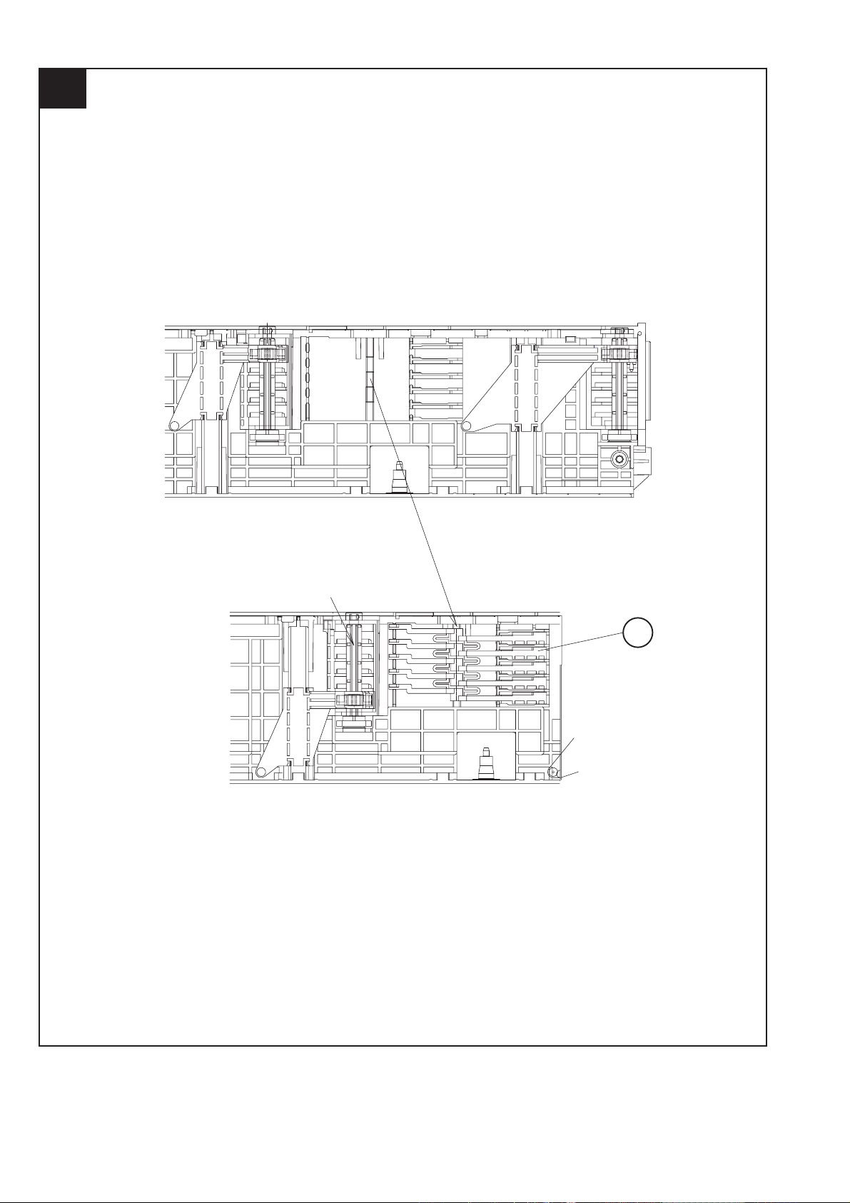
3. CHANGER MECHANISM SECTION
Perform steps 1, 2, 9 and 10 of the disassembly
method to remove the CD changer mechanism.
3.1. How to remove CD Disc (See Fig. 2~5)
1. When CD is at play position (Figure 2), rotate reduction gear C clock-wise as shown in Figure 3 Until
disc tray is at stock position, then rotate further to
eject the disc tray so that CD can be removed from
the tray.
Disc Tray
Guide Tray
CD at play position.
CD Disc
CD Disc
Up Down
Figure 4
Gear up down board
Mark 1
(DISC 1)
Figure 5
Mark 3 Mark 5
(DISC 3)
Mark 2
(DISC 2)
(DISC 5)
Mark 4
(DISC 4)
CD at stalk position.
Figure 2
3 – 5
Page 48

CD-MPX870W
r
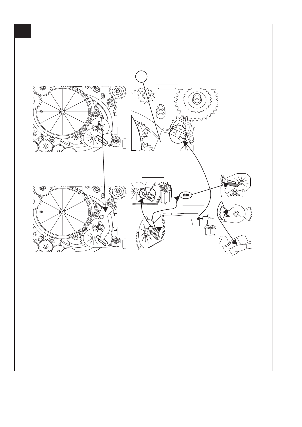
3.2. How to Remove the tray motor/main cam
motor/5-Changer Motor PWB (See Fig. 1)
1. Remove the screws (A1) x 2 pcs., to remove tray
motor/main cam motor/5-Changer Motor PWB.
Changer Mechanism Unit
Main Cam Motor
(A1)X2
φ2x10mm
Figure 1
Tray Moto
5-Changer
Motor PWB
NOTE:There are 2 more screws tighten the motors at
the bottom of main chassis. Before performing
procedure 1 above, disc stop spring, top plate
sear up down board and trays must be
removed, then only the 2 screws can be
untighten.
3 – 6
Page 49

CHAPTER 4. DIAGRAMS
[1] CD Block diagram
CD-MPX870W
XL1
16.9344 MHz
+3.3V
CONSTANT
VOLTAGE
TO MAIN SECTION
R-CH
AGND
L-CH
CE
43
CL
44
DI
45
DO
46
RESB
47
INTB0
48
INTB1
49
XOUT
72
XIN
73
DVDD
AVDD
36 41
+3.3V
D_+5V(+B5)
DGND
7875
LCHO
RCHO
+8V(+B7)
MGND
7 1 2 3 4 5 6
CNP3
LC78690E
CD SERVO
XVDD
74
LRVDD
76 876521
IC1
Q1
TO DISPLAY SECTION
+B6
GND
PHOTO
MO_A-
DIN
BIN
CIN
AIN
LASER
DRIVER
CD_RESB
MO_A+
CONT1
EIN
1413
CD_CLK
5251
CONT0
FIN
MP3_INT11CD_INT12TRAY SW1/SW2
CD_DI
CD_DO
CD_CE
10
PUIN
SLDO
SPDO
FDO
TDO
LDD
LDS
18 1968
13
77
71
67
57
56
55
54
53
42
40
37
26
20
32
24
25
22
23
DISC/CLAMP
143 1 9 8 7 6 52 4
CNP7
+5V
SW3 TRAY SW2
SW2 TRAY SW1
SW1 CLAMP
SW4 DISC
RX1
GND
17151311
22
23
VIN4
VIN3
VIN2
VIN1
28
PVCC2
REV6
IC2
FWD6
LA6261
FOCUS/TRACKING/
9
27
SPIN/SLIDE
DRIVER
M1
M1
MAIN CAM
TRAY MOTOR
M
M
+
+
--
10 113 1 9 8 7 6 52 4
32 3331 34
VO6-
VO6+
VO5+
FWD5
REV5
MOTOR
CNP4
VO5-
19
20
30
7
26
PICKUP UNIT
+3.3V
COIL
TRACKING
FOCUS COIL
Figure 4-1: CD BLOCK DIAGRAM
4 – 1
NM1
SPINDLE
MOTOR
NM2
SLED
MOTOR
M
M
4
3363521
56
NSW 1
PICKUP
IN
Page 50

CD-MPX870W
VF1
MUTE
[2] Main Block diagrams
CHASIS_GND
11
CNP303
REC.
FM_DET
10
TUN_SM
9
R_CH
8
+9V
7
L_CH
6
CHASIS_GND
5
DO
4
CL
3
DI
2
CE
1
1
2
3
+B4
+B3
+B3
FROM CD SECTION
TAPE 1
P.B. HEAD
TAPE 2
REC./P.B.
HEAD
L-CH
R-CH
L-CH
R-CH
NC
NO USE
MOTOR
DRIVER
Q707~
Q709
Q703~
Q706
Q710
Q711
SOLENOID
DRIVER
CNP2
P.B.
AC BIAS
ERASE
HEAD
TAPE
MECHANISM
ASS'Y
VIDEO OUT
BI601CNS601
1
3
4
SWITCHING
Q101~
Q104
Q105
Q106
JK691
L(T1)
R(T1)
L(T2)
R(T2)
POP REDUCE
L REC.
R REC.
SWITCHING
+B4
Q112
SWITCHING
Q111
L103
BIAS
OSC
1
24
2
23
6
T1/T2
REC
9
16
11
12
NOR/
15
HIGH
Q114
SWITCHING
SPAN SELECTOR
SW601
JK690
GAME INPUT
R
L
VIDEO
13
P.B.
4
21
H/N
7
18
10
T1/T2
19
Q113
Q109
SWITCHING
TUNER
PACK
UNIT
RTUNSA007AWZZ
NC
9
TAPE
CD
L
16
R
L
10
15
R
L
11
14
R
L
12
13
R
L
R
L
R
AUX
TUNERTUNER
+B4
P.B.
REC.
IC101
AN7345K
PLAYBACK AND RECORD/
ALC
PLAYBACK AMP.
+B4
Q110
BIAS
+B4
SPAN
+B4
23
1
DI
2
CE
24
LED
Q702
CLK
3
Q107
Q108
MUTING
21
4
43
-20dB
ATT
R
L
IXA101AW
IC601
LC75341
AUDIO PROCESSOR
18
7
ILLUSION
LED701
MICROCOMPUTER
REC/PLAY
JOG701
VOLUME
5
IC701
SYSTEM
(2/2)
SYSTEM
Q665
T1/T2
BIAS
Figure 4-2: MAIN BLOCK DIAGRAM (1/2)
4 – 2
Page 51

FL701
FL DISPLAY
812 45
26
25
~
CD-MPX870W
47
~
5150
TAPE
MECHANISM
ASS'Y
665
MUTE
SYSTEM
SP DET.
D905~D907
IC901
STK412-420
POWER AMP.
18
L
14
R
7
1
5
2
6
-B1
57
~
78
80
VLOAD
8
SPAN
81
~
98
99
100
1 54515253
+B8
L-OUT
11
8
R-OUT
+B1
+B8
79
26 3837 394055
VDD
IC701
IXA101AW
SYSTEM
MICROCOMPUTER
(1/2)
AVDD
RESET
RESET
1011
16 1742 1312 20 23 28 29 30 31
XL701
4.19 MHz
Q712
Q901~
Q904
+B8
18
VDD
+B8
SP RELAY
ON-OFF
D801
~
15 14
VDD
CLK
CEDIDO
Q905
RL914
27
1
+B8
41
2
~~
4
34
32
25
36
Q906
DRIVER
FAN MOTOR
RX701
REMOTE
SENSOR
SW701-SW705
SW707-SW716
3
2
KEY
TO CD
SECTION
+B5
M901
M
MOTOR
SO901
SPEAKER
TERMINAL
+B3
JK692
HEADPHONES
PT801
MAIN POWER
TRANSFORMER
+B8
FAN
T1/T2
BIAS
ER
VF1
UN
SW_5.6V
+B8
-VF
VF2
+B3
+B7
+B4
+B9
+B6
+B8
2
IC854
3
KIA78L05
VOLTAGE
REGULATOR
-B2
+B2
LD+8V
M+13V
A+10V
A_+5V
SW5V
D+5V
RELAY
DRIVER
1
AN80T53
MULTI REGULATOR
7
2
6
+5V
1
D856
1SS119
Figure 4-3: MAIN BLOCK DIAGRAM (2/2)
IC851
D802
3
4 – 3
T5AL250V
F801
T5AL250V
D803,
D804
Q801
F802
T2AL250V
F803
T2AL250V
VOLTAGE
REGULATOR
F804
T.F.
F807
T2•5AL250V
F806
T2•5AL250V
SW801
VOLTAGE
SELECTOR
230-240V
220V
127V
110V
AC POWER SUPPLY CORD
AC110/127/220/230-240V.
F805
T5AL250V
50/60 Hz
Page 52

CD-MPX870W
CHAPTER 5. CIRCUIT DESCRIPTION
[1] Waveforms of CD Circuit
1
1
2
3
IC1 22
IC1 23
IC1 22
IC1 16
Stopped
CH1=500 mV
DC 10:1
T
FDO
1
TDO
3
Smoothing : ON CH1 : 0.000 V
BW : FULL
Stopped
1
T
2
3
-3 div -1 div 0 div +1 div +3 div
Smoothing : ON CH1 : 0.000 V
BW : FULL
CH1=500 mV
DC 10:1
FDO
TE
CH2 : 0.0 V
CH3 : 0.000 V
CH4 : 0.00 V
CH2=10 V
DC 10:1
CH Position To
CH2 : 0.0 V
CH3 : 0.00 V
CH4 : 0.00 V
CH3=500 mV
DC 10:1
=Record Length=
Main : 100 K
Zoom : 2 K
CH3=1 V
DC 10:1
=Record Length=
Main : 100 K
Zoom : 2 K
500 ms/div
(500 ms/div)
NORM:20 kS/s
CH1
v/DIV
500 mV
=Trigger==Filter= =Offset=
Mode : AUTO
Type : EDGE CH1
Delay : 0.0 ns
Hold off : 0.2 µs
500 ms/div
(500 ms/div)
NORM:20 kS/s
CH2
Position
0.20 div
=Trigger==Filter= =Offset=
Mode : AUTO
Type : EDGE CH1
Delay : 0.0 ns
Hold off : 0.2 µs
1
5
6
7
1
IC1 22
IC1 25
IC1 28
IC1 27
IC1 22
Stopped
CH1=200 mV
DC 10:1
T
FDO
2
SPDO
1
=Filter= =Offset=
Smoothing : ON CH1 : 0.000 V
BW : FULL
Stopped
CH1=500 mV
DC 10:1
PD00
3
4
PD01
T
FDO
1
Smoothing : ON CH1 : 0.000 V
BW : FULL
T
CH2=500 mV
DC 10:1
CH2 : 0.000 V
CH3 : 0.00 V
CH4 : 0.00 V
CH2 : 0.0 V
CH3 : 0.00 V
CH4 : 0.00 V
=Record Length=
Main : 100 K
Zoom : 2 K
CH3=1 V
DC 10:1
=Record Length=
Main : 100 K
Zoom : 2 K
1999/04/07 09:51:15
500 ms/div
(500 ms/div)
NORM:20 kS/s
=Trigger=
Mode : NORMAL
Type : EDGE CH2
Delay : 2.924 ms
Hold off : 0.2 µs
1999/04/05 17:33:17
CH4=1 V
500 ms/div
(500 ms/div)
DC 10:1
NORM:20 kS/s
=Trigger==Filter= =Offset=
Mode : AUTO
Type : EDGE CH2
Delay : 0.0 ns
Hold off : 0.2 µs
CH1
v/DIV
500 mV
IC1 2
4
Vp-p=1.0 V~1.3 V
0.5 mV/div,0.5 µsec/div
5 – 1
Page 53

[2] Voltage
CD-MPX870W
IC701
PIN PIN
VOLTAGE
NO NO
1 4.94 V
4.94 V
2 52 4.40 V
353
4.92 V
4.92 V
454
1.32 V
555
4.92 V
656
4.92 V
7 57 -29.05 V
8 0.00 V
9 4.87 V
4.87 V
10 60
4.87 V
11 61
0.00 V
12 62
0.00 V
13 63
0.00 V
14 64
0.00 V
15 65
0.00 V
16 66
0.00 V
17 67
0.00 V
18 68
0.00 V
19 69
20 70
0.00 V
0.00 V
21 71
22 4.52 V 72
23 4.41 V 73
24 4.54 V
0.00 V
25 75
0.00 V
26 76
27 1.87 V 77
4.05 V
28 78
4.07 V
29 79
0.00 V
30 80
31 4.66 V 81
32 0.23 V 82
33 4.95 V 83
34 4.95 V 84
35 85
0.00 V
0.00 V
36 86
37 13.15 V
13.15 V
38 88
13.15 V
39 89
0.00 V
40 90
41 -23.60 V 91
42 4.72 V 92
43 4.41 V
4.54 V
44 94
45 0.00 V 95
0.00 V
46 96
0.00 V
47 97
0.00 V
48 98
49 4.54 V 99
50 0.00 V 100
51
58
59
74
87
93
VOLTAGE
0.00 V
4.38 V
0.00 V
4.39 V
4.43 V
-26.42 V
-18.41 V
-29.08 V
-29.08 V
0.00 V
-29.08 V
-0.92 V
-0.96 V
-11.10 V
0.00 V
-23.60 V
-29.00 V
-23.60 V
0.00 V
0.00 V
-23.60 V
-26.20 V
-23.60 V
0.00 V
-26.40 V
0.00 V
-23.60 V
0.00 V
-23.61 V
-20.84 V
-10.43 V
-23.50 V
-26.40 V
-28.93 V
-26.40 V
-21.10 V
-25.12 V
-24.99 V
-23.01 V
-25.00 V
-24.98 V
-25.00 V
-24.85 V
-24.92 V
-24.89 V
-24.82 V
-24.87 V
-24.63 V
IC1IC 601
PIN
NO
10 13.2 510 12.1
2 0 2 1.61 52 0 2 2.2
3 0 3 1.61 53 0 3 2.1
44.98 4 1.6 54 0 4 2.2
5 4.95 5 1.61 55 0 5 2.1
6 4.96 6 3.06 56 0 6 2.2
7 4.99 7 1.65 57 0 7 0
8 4.96 8 1.65 58 0 8 4.37
9 4.96 9 1.65 59 0 9 5.02
10 4.99 10 1.65 60 3.2 10 3.2
11 4.96 11 1.48 61 0 11 1.62
12 4.96 12 0 62 0 12 1.65
13 4.96 13 1.65 63 0.53 13 1.62
14 4.96 14 0 64 0 14 1.65
15 4.96 15 1.65 65 5.18 15 1.62
16 4.96 16 1.47 66 5.18 16 0
17 4.99 17 1.48 67 4.68 17 1.62
18 4.96 18 0 68 0 18 1.64
19 4.96 19 0 69 0 19 4.71
20 4.96 20 0 70 0 20 4.71
21 4.96 21 1.6 71 0 21 3.92
22 4.98 22 0 72 0 22 3.11
23 9.95 23 1.61 73 0 23 3.1
24 0 24 1.61 74 4.68 24 2.5
IC 901
PIN
VOLTAGE
NO
1 58.3 29 3.2 79 0 29 5.02
2 24.85 30 0 80 3.2 30 0.69
3 12.79 31 0 31 0.71
4 -12.85 32 1.59 32 0
5 -24.75 33 1.6 PIN
6 -58.9 34 3.2
70 350 10 352.11
80 360 20 362.2
90 370 30
10 0 38 0 4 2
11 0 39 0 5 2
12 -57.4 40 0 6 1.32 PIN
13 57.6 41 3.61 7 0
14 0 42 0 8 0.6 1 2.55
15 0 43 0 9 3.48 2 2.55
16 -56.01 44 1.8 10 3.44 3 2.55
17 0 45 3.8 11 0 4 0
18 0 46 0 12 0 5 2.49
IC 851
PIN
VOLTAGE
NO
1 5.06 17 0.6
2 12.83 18 0
3 19.6 19 2.59
40 20 2
5 18.28 21 2
69.92 22 0
78.4 23 0
PIN
VOLTAGEVOLTAGE
NO
25 0 75 4.68 25 1.65
26 0 76 3.01 26 0
27 3.2 77 0 27
28 0 78 1.12 28
47 1.45 13 6.9 6 2.69
48 1.49 14 4.18 7 1.34
49 3.19 15 0 8 12.66
50 3.79 16 3.45
PIN
VOLTAGE VOLTAGE
NO
IC101
VOLTAGE
NO
24 0
IC2
PIN
NO
33 0
34 0
IC 503
VOLTAGE
NO
5.02
8.68
5 – 2
Page 54

CD-MPX870W
-MEMO-
5 – 3
Page 55

CD-MPX870W
CHAPTER 6. CIRCUIT SCHEMATICS AND PARTS LAYOUT
[1] Notes on schematic diagram
• Resistor:
To differentiate the units of resistors, such symbol
as K and M are used: the symbol K means 1000
ohm and the symbol M means 1000 kohm and the
resistor without any symbol is ohm-type resistor.
Besides, the one with “Fusible” is a fuse type.
• Capacitor:
To indicate the unit of capacitor, a symbol P is used:
this symbol P means pico-farad and the unit of the
capacitor without such a symbol is micr ofarad. As to
electrolytic capacitor, the expression “capacitance/
withstand voltage” is used.
(CH), (TH), (RH), (UJ): Temperature compensation
(ML): Mylar type
(P.P.): Polypropylene type
• Schematic diagram and Wiring Side of P.W.Board
for this model are subject to change for improvement without prior notice.
• The indicated voltage in each section is the one
measured by Digital Multimeter between such a
section and the chassis with no signal given.
1. In the tuner section,
indicates AM
indicates FM stereo
2. In the main section, a tape is being played back.
3. In the deck section, a tape is being played back.
( ) indicates the record state.
4. In the power section, a tape is being played back.
5. In the CD section, the CD is stopped.
• Parts marked with “ “ ( ) are impor-
tant for maintaining the safety of the set. Be sure to
replace these parts with specified ones for maintaining the safety and performance of the set.
REF. NO DESCRIPTION POSITION
JOG701 VOLUME MAX—MIN
SW701 POWER ON /STAND-BY ON—OFF
SW702 CD ON—OFF
SW703 TUNER (BAND) ON—OFF
SW704 AUX ON—OFF
SW705 TAPE ON—OFF
SW707 PLAY ON—OFF
SW708 FAST FORWARD/PRESET UP ON—OFF
[2] Types of transistor and LED
REF. NO DESCRIPTION POSITION
SW709 FAST REWIND/PRESET DOWN ON—OFF
SW710 STOP ON—OFF
SW711 DISC 1 ON—OFF
SW712 DISC 2 ON—OFF
SW713 DISC 3 ON—OFF
SW714 DISC 4 ON—OFF
SW715 DISC 5 ON—OFF
SW716 OPEN/CLOSE ON—OFF
D1SS119
6 – 1
Page 56

CD-MPX870W
[3] Schematic diagram
Figure 6-2: MAIN SCHEMATIC DIAGRAM (1/2)
6 – 2
Page 57

CD-MPX870W
Figure 6-3: MAIN SCHEMATIC DIAGRAM (2/8)
6 – 3
Page 58

CD-MPX870W
Figure 6-4: POWER SCHEMATIC DIAGRAM (3/8)
6 – 4
Page 59

CD-MPX870W
Figure 6-5: POWER SCHEMATIC DIAGRAM (4/8)
6 – 5
Page 60

CD-MPX870W
Figure 6-6: DISPLAY SCHEMATIC DIAGRAM (5/8)
6 – 6
Page 61

CD-MPX870W
Figure 6-7: DISPLAY SCHEMATIC DIAGRAM (6/8)
6 – 7
Page 62

CD-MPX870W
Figure 6-8: CD SERVO SCHEMATIC DIAGRAM (7/8)
6 – 8
Page 63

CD-MPX870W
Figure 6-9: CD SERVO SCHEMATIC DIAGRAM (8/8)
6 – 9
Page 64

CD-MPX870W
[4] Wiring side of PWB
Figure 6-10: WIRING SIDE OF MAIN PWB (TOP VIEW) (1/15)
6 – 10
Page 65

CD-MPX870W
Figure 6-11: WIRING SIDE OF MAIN PWB (TOP VIEW) (2/15)
6 – 11
Page 66

CD-MPX870W
Figure 6-12: WIRING SIDE OF MAIN PWB (BOTTOM VIEW) (3/15)
6 – 12
Page 67

CD-MPX870W
Figure 6-13: WIRING SIDE OF MAIN PWB (BOTTOM VIEW) (4/15)
6 – 13
Page 68

CD-MPX870W
-MEMO-
6 – 14
Page 69

CD-MPX870W
Figure 6-14: WIRING SIDE OF POWER PWB (5/15)
6 – 15
Page 70

CD-MPX870W
Figure 6-15: WIRING SIDE OF DISPLAY PWB (TOP VIEW) (6/15)
6 – 16
Page 71

CD-MPX870W
Figure 6-16: WIRING SIDE OF DISPLAY PWB (TOP VIEW) (7/15)
6 – 17
Page 72

CD-MPX870W
Figure 6-17: WIRING SIDE OF DISPLAY PWB (BOTTOM VIEW) (8/15)
6 – 18
Page 73

CD-MPX870W
Figure 6-18: WIRING SIDE OF DISPLAY PWB (BOTTOM VIEW) (9/15)
6 – 19
Page 74

CD-MPX870W
Figure 6-19: WIRING SIDE OF GAME INPUT PWB (TOP VIEW) (10/15)
6 – 20
Page 75

CD-MPX870W
Figure 6-20: WIRING SIDE OF GAME INPUT PWB (BOTTOM VIEW) (11/15)
6 – 21
Page 76

CD-MPX870W
Figure 6-21: WIRING SIDE OF CD SERVO PWB (TOP VIEW) (12/15)
6 – 22
Page 77

CD-MPX870W
Figure 6-22: WIRING SIDE OF CD SERVO PWB (TOP VIEW) (13/15)
6 – 23
Page 78

CD-MPX870W
Figure 6-23: WIRING SIDE OF CD SERVO PWB (BOTTOM VIEW) (14/15)
6 – 24
Page 79

CD-MPX870W
Figure 6-24: WIRING SIDE OF PWB (15/15)
6 – 25
Page 80

CD-MPX870W
CHAPTER 7. FLOWCHART
[1] Troubleshooting
1. When the CD does not function
The CD section may not operate when the objective lens of the optical pickup is dirty. Clean the objective lens, and
check the playback operation. When this section do es not opera te even af ter the above step is t aken, check the follo wing items.
Remove the cabinet and follow the trouble shootin g instructions.
"Track skipping and/or no T OC (Table Of Contents) may be caused by build up of dust other foreign matter on the laser
pickup lens. Before attempting any adjustment make certain that the lens is clean. If not, clean it as mentio ned below."
Turn the power off.
Gently clean the lens with a lens cleaning tissue and a small amount of isopropyl alcohol.
Do not touch the lens with the bare hand.
Parts code
1. CD optical pickup Lens cleaner disc UDSKA0004AFZZ
HOW TO USE
1.
Using the brush in the cleaner cap, apply 1 or 2 drops of the cleaning fluid to the
brush on the CD cleaner disc which has the mark next to it.
2.
Place the CD cleaner disc onto the CD disc tray with the brush side down, then
press the play button.
3.
You will hear music for about 20 seconds and the CD player will automatically stop.
If it still play continuously, press the stop button.
CAUTION
The CD lens cleaner should be effective for 30-50 operations, however if the
brushes become worn out earlier then please replace the cleaner disc.
If the CD cleaner brushes become very wet then wipe off any excess fluid with a soft
cloth.
Do not drink the cleaner fluid or allow it contact with the eyes. In the event of this
happening then drink and / or rinse with clean water and seek medical advice.
The CD cleaner disc must not be used on car CD players or on computer CD-ROM
drives.
All rights reserved. Unauthorized duplicating, broadcasting and renting this product
is prohibited by law.
2. When a CD cannot be played
Cleaning fluid
Cleaner disc
2.1. Pressing the CD operation key is accepted, but playback does not occur.
1) Focus-HF system check
2) Tracking system check
3) Spin system check
4) PLL system check
5) Others
7 – 1
Page 81

(1) Focus-HF system check.
Although a CD is inserted and the cover is closed,
"NO DISC" is displayed.
Press the Tray1 CD Eject Button without inserting a disc, and try
starting the playback operation.
Stopped
CH1=500 mV
DC 10:1
T
FDO
1
TDO
3
Smoothing : ON CH1 : 0.000 V
BW : FULL
CH2 : 0.0 V
CH3 : 0.000 V
CH4 : 0.00 V
CH3=500 mV
DC 10:1
=Record Length=
Main : 100 K
Zoom : 2 K
Figure 1
CD-MPX870W
500 ms/div
(500 ms/div)
NORM:20 kS/s
CH1
v/DIV
500 mV
=Trigger==Filter= =Offset=
Mode : AUTO
Type : EDGE CH1
Delay : 0.0 ns
Hold off : 0.2 µs
1. Does the pickup move to the PICKUP-IN Switch (NSW1)
No Sled motor (NM2).
position ?
Yes
2. Does the focus (lens) move up and down ?
No Check the focus peripheral circuit.
(Waveform drawing Figure 1)
Yes
3. Is the laser lit ? No Check the laser diode driver Q1 peripheral circuit.
Yes
4. Is the turntable rotating ? No Spindle motor (NM1).
When a disc is loaded, start playback operation.
1. Is focus servo activated ?
(Waveform drawing Figure 2)
No Pins 5~9, 11, 18 and 19 on IC1
Check the laser diode driver Q1 peripheral circuit.
Yes
2. Is the HF waveform normal ?
No If the level is not nor mal.
(Waveform drawing Figure 3)
Stopped
CH1=500 mV
CH2=10 V
DC 10:1
CH3=1 V
DC 10:1
=Record Length=
Main : 100 K
Zoom : 2 K
DC 10:1
FDO
1
T
2
TE
3
-3 div -1 div 0 div +1 div +3 div
Smoothing : ON CH1 : 0.000 V
BW : FULL
CH Position To
CH2 : 0.0 V
CH3 : 0.00 V
CH4 : 0.00 V
Figure 2
500 ms/div
(500 ms/div)
NORM:20 kS/s
CH2
Position
0.20 div
=Trigger==Filter= =Offset=
Mode : AUTO
Type : EDGE CH1
Delay : 0.0 ns
Hold off : 0.2 µs
7 – 2
Figure 3
Vp-p=1.0 V~1.3 V
0.5 mV/div,0.5 µsec/div
Page 82

CD-MPX870W
(2) Tracking system check.
Check the TE waveform at pin 16 on IC1.
If the waveform shown in Figure 4 appears and soon after NO
DISC appears ?
Yes
No
"Initialization" is possible, but play is not possible ?
Yes
No
"Initialization" is not possible. Data cannot be read. Check the VCO-PLL (Pin26~30 on IC1)
The tracking servo is not activated.
Check the peripheral circuits at pins 15, 16 and 23 on IC1,
and FFC1.
A normal jump operation cannot be completed or the beginning of the track cannot be found.
Check the around pin 23 on IC1.
system.
(3) Spin system check.
Press the OPEN/CLOSE switch without inserting a disc, and
then try starting the play operation.
1. The turntable rotates a little ?
(Waveform drawing Figure 5)
Stopped
CH1=10 V
DC 10:1
TE
2
DRF
T
1
Smoothing : ON CH1 : 0.0 V
BW : FULL
T
CH2=1 V
DC 10:1
CH2 : 0.00 V
CH3 : 0.00 V
CH4 : 0.00 V
Figure 4
Yes The spin driver circuit is OK.
=Record Length=
Main : 100 K
Zoom : 2 K
100 ms/div
(100 ms/div)
NORM:100 kS/s
=Trigger==Filter= =Offset=
Mode : NORMAL
Type : EDGE CH1
Delay : 2.924 ms
Hold off : 0.2 µs
No
2. The turntable doesn't rotate. Check around pin 25 on IC1, pins 5 and 6 on CNP2.
Stopped
CH1=200 mV
DC 10:1
T
PDOUT 0
2
PDOUT 1
1
=Filter= =Offset=
Smoothing : ON CH1 : 0.000 V
BW : FULL
T
CH2=500 mV
DC 10:1
CH2 : 0.000 V
CH3 : 0.00 V
CH4 : 0.00 V
=Record Length=
Main : 100 K
Zoom : 2 K
1999/04/07 09:51:15
500 ms/div
(500 ms/div)
NORM:20 kS/s
=Trigger=
Mode : NORMAL
Type : EDGE CH2
Delay : 2.924 ms
Hold off : 0.2 µs
Figure 5
7 – 3
Page 83

CD-MPX870W
(4) PLL system check.
When a disc is loaded, start play operation.
The HF waveform is normal, but the TOC data cannot be read.
Check the PDOUT waveform. (Figure 6)
Check around pins 26~30 on IC1.
Stopped
CH1=500 mV
DC 10:1
PDO0
3
4
PDO1
T
FDO
1
Smoothing : ON CH1 : 0.000 V
BW : FULL
CH2 : 0.0 V
CH3 : 0.00 V
CH4 : 0.00 V
CH3=1 V
DC 10:1
=Record Length=
Main : 100 K
Zoom : 2 K
1999/04/05 17:33:17
CH4=1 V
500 ms/div
(500 ms/div)
DC 10:1
NORM:20 kS/s
=Trigger==Filter= =Offset=
Mode : AUTO
Type : EDGE CH2
Delay : 0.0 ns
Hold off : 0.2 µs
CH1
v/DIV
500 mV
Figure 6
(5) Others.
The HF waveform is normal and the time is
displayed normally, but no sound is produced. Or
the sound has dropouts.
Is pin 35 (C2F) on IC1 "L" ? No There are too many error flags on a damaged disc which makes
error correction impossible.
Yes
1. When playing at normal speed.
Check the peripheral circuit at pin 69 (DOUT) on IC1 and the
waveform (Figure 7).
If OK, Check the unit.
Check again using a known good disc.
DOUT
CH1=2 V
DC 10:1
T
CH2 : 0.00 V
CH3 : 0.00 V
CH4 : 0.00 V
=Record Length=
Main : 1 K
Zoom : 100
Stopped
T
1
Smoothing : ON CH1 : 0.00 V
BW : FULL
1999/04/07 09:25:28
500 ns/div
(500 ns/div)
NORM:200 MS/s
=Trigger==Filter= =Offset=
Mode : NORMAL
Type : EDGE CH1
Delay : 2.887 ms
Hold off : 0.2 µs
7 – 4
Figure 7
Page 84

CD-MPX870W
CHAPTER 8. OTHERS
[1] Function table of IC
IC1 VHiLC78690E-1: CD Servo (LC78690E) (1/2)
Pin No. Terminal Name Input/Output Setting in Reset Function
1 EFMIN Input INPUT RF signal input pin.
2 RFOUT Output UNSTABLE RF signal output pin.
3 LPF Output UNSTABLE RF signal DC level detection. LPF capacitor connection pin.
4 PHLPF Output UNSTABLE LPF capacitor pin for detection problem.
5 AIN Input INPUT A signal input pin.
6 CIN Input INPUT C signal input pin.
7 BIN Input INPUT B signal input pin.
8 DIN Input INPUT D signal input pin.
9 FEC Output UNSTABLE FE signal LPF capacitor connection pin.
10* RFMON Output UNSTABLE Built in analog signal for monitoring LSI pin.
11 VREF Output AVDD/2 VREF voltage output pin.
12 JITTC Output UNSTABLE Jitter detection capacitor connection pin.
13 EIN Input INPUT E signal input pin.
14 FIN Input INPUT F signal input pin.
15 TEC Output UNSTABLE TE signal LPF capacitor connection pin.
16 TE Output UNSTABLE TE signal output pin.
17 TEIN Input INPUT TES signal generation TE signal input pin.
18 LDD Output UNSTABLE Laser power control signal output pin.
19 LDS Input INPUT Laser power control signal input pin.
20 AVSS — — Analog GND pin. This pin must always be connected to 0V.
21 AVDD — — Analog power supply pin.
22 FDO Output AVDD/2 Focus control output pin. D/A converter output.
23 TDO Output AVDD/2 Tracking control output pin. D/A converter output.
24 SLDO Output AVDD/2 SLED control output pin. D/A converter output.
25 SPDO Output AVDD/2 SPINDLE control output pin. D/A converter output.
26 VVSS1 — — For use
27 PDOUT1 Output UNSTABLE Phase comparison output pin 1 to control built in VCO.
28 PDOUT0 Output UNSTABLE Phase comparison output pin 0 to control built in VCO.
29 PCKIST Input INPUT Resistor connection pin to set current for PDOUT 0 and 1 output.
30 VVDD1 — — Built_in VCO power supply pin 1.
by the
EFM
PLL
Circuit
Built-in VCO GND pin. This pin must always be connected to 0V.
31* DMUTEB Output L DMUTEB output pin.
32 PUIN Input/Output INPUT PUIN input pin. (built-in pull-up resistor)
33* DEFECT Output L DEFECT signal output pin.
34* FSEQ Output L Detected sync signal output. This signal is high when the sync signal
detected from the EFM signal and the internally generated sync signal
agree.
35* C2F Output L C2 error flag monitor output pin.
36 DVDD — — Digital power supply pin.
37 DVSS — — Digital GND pin. This pin must always be connected to 0V.
38 DVDD1.8 Output H Supply voltage connect to capacitor for digital circuit.
39 VDD3 — — Built-in VCO power supply pin 3.
40 VVSS3 — — Built-in VCO GND pin 3. This pin must always be connected to 0V.
41 DVDD — — Digital power supply pin.
42 DVSS — — Digital GND pin. This pin must always be connected to 0V.
43 CE Input INPUT Micro44 CL Input INPUT Data transfer clock input pin.
45 DI Input INPUT Data input pin.
46 DO Output H Data output pin. (TRI-State Output)
47 RESB Input — Reset input pin for LSI. This pin must set to low briefly after power is
48 INTB0 Output H Interrupt signal output pin 0. (SERVO Section)
49 INTB1 Output H Interrupt signal output pin 1. (DECODER Section)
50 ICONT2 Input/Output INPUT General Purpose I/O pin 2 Controlled by command from the
In this unit, the terminal with asterisk mark (*) is (open) terminal which is not connected to the outside.
Com-
puter
Inter-
face
applied.
Chip enable signal input pin.
microprocessor. Any of these that are unused
must be either set up as input pin ports and
connected to 0V, or set up as output pin ports
and left open.
8 – 1
Page 85

CD-MPX870W
IC1 VHiLC78690E-1: CD Servo (LC78690E) (2/2)
Pin No. Terminal Name Input/Output Setting in Reset Function
51 CONT1 Input/Output INPUT General Purpose I/O pin 1 Controlled by command from the microproces52 CONT0 Input/Output INPUT General Purpose I/O pin 0
53 TEST0 Input L Test input pin 1. This pin must always be connected to 0V.
54 STREQ Input/Output INPUT Stream data request output pin.
55 STCK Input/Output INPUT Stream data bit clock usage input pin.
56 STDATA Input/Output INPUT Stream data input pin.
57 TEST1 Input L Test input pin 0. This pin must always be connected to 0V.
58* DATA Output L Left/Right clock output pin.
59* DATACK Output L Bit clock output pin.
60* LRSY Output L Left/Right channel data output pin.
61 VVDD2 — — For use by
62 VPREF2 Input INPUT Built-in VCO control oscillator range setting input pin.
63 VCOC2 Input INPUT Built-in VCO control voltage setting input pin.
64 VPDOUT2 Output UNSTABLE Built-in VCO control output pin 2.
65 VVSS2 — — Built-in VCO GND pin. This pin must always be connected to
66 DVDD1.8 Output H Supply voltage connect to condenser for digital circuit.
67 DVSS — — Digital GND pin. This pin must always be connected to 0V.
68 DVDD — — Digital power supply pin.
69* DOUT Output Input Digital output pin. EIAJ format.
70* AMUTEB Output L GAMUTEB output pin.
71 XVSS — — Digital GND pin. This pin must always be connected to 0V.
72 XOUT Output OSCILLATING Crystal
73 XIN Input OSCILLATING
74 XVDD — — Digital power supply pin.
75 LCHO Output LRVDD/2 D/A con76 LRVDD — — LR channel power supply pin.
77 LRVSS — — LR channel GND pin. This pin must always be connected to
78 RCHO Output LRVDD/2 Right channel input supply pin.
79 AVDD — — Analog power supply pin.
80 SLCO — — Slice level control output pin.
In this unit, the terminal with asterisk mark (*) is (open) terminal which is not connected to the outside.
the EFM
PLL Circuit
oscillator
verter
Built-in VCO power supply pin 2.
0V.
Connections for a 16.9344 MHZ oscillator element.
Left channel output supply pin.
0V.
sor. Any of these that are unused must be
either set up as input pin ports and connected
to 0V, or set up as output pin ports and left
open.
8 – 2
Page 86

CD-MPX870W
A
IC1 VHiLC78690E-1: CD Servo (LC78690E)
LRVSS
RCH0
AVD D
SLC0
LRVDD
LCH0
XIN
XVDD
XVSS
XOUT
DVD D
DOUT
AMUTEB
DVSS
VVSS2
DVDD1.8
VPREF2
VCOC2
VPDOUT2
VVDD2
EFMIN
RFOUT
LPF
PHLPF
AIN
CIN
BIN
DIN
FEC
RFMON
VREF
JITTC
EIN
FIN
TEC
TEIN
LDD
LDS
AVSS
TE
80 79 78 77 76 75 74 73
72
7071 69 6867 66 636465 62 61
1
2
3
4
5
6
7
8
9
10
LC78690E
11
12
13
14
15
16
17
18
19
20
21 22 23 24 25 26 27 28 29 3130 32 33 34 35 36 37 38 39 40
FD0
AVDD
TD0
SLD0
SPD0
VVSS1
PDOUT1
PCKIST
PDOUT0
VVDD1
DMUTEB
PUIN
FSEQ
DEFECT
C2F
60
LRSY
DATACK
59
58
DATA
57
TEST1
56
STDATA
55
STCK
54
STREQ
53
TEST0
52
CONT0
51
CONT1
50
CONT2
49
INTB1
48
INTB0
47
RESB
46
DO
45
DI
44
CL
43
CE
42
DVSS
41
DVD D
DVSS
DVD D
VVDD3
DVDD1.8
VVSS3
EFMIN
RFOUT
LPF
PHLPF
AIN
CIN
BIN
DIN
FEC
RFMON
VREF
JITTC
EIN
FIN
TEC
TEIN
LDD
LDS
AVSS
TE
AVD D
SLC0
SLICE LEVEL
CONTROL
RF
SIGNAL
PROCESSOR
VREF
MONITOR
TES,HFL,
DEFECT
JITTER
APC
FD0
AVD D
RCH0
TD0
LRVSS
LPF
SLD0
LRVDD
CONTROL
SPD0
XOUT
XIN
XVDD
LCH0
CLOCK
GENERATOR
1bit DAC
8FS DIGITAL FILTER
DEEMPHASIS
ATTENUATION CONTROL
INTERPOLATION MUTE
Audio FLT MUTE
Synchronization
Detection
EFM
Demodulation
SERVO
A/D
D/A
CD PLL
VVSS1
PDOUT1
PDOUT0
PCKIST
DOUT
AMUTEB
XVSS
DOUT
MP3 & WMA
DECODER
TEXT
SUBCODE DECODE
PUIN
VVDD1
DMUTEB
DVSS
DVD D
Memory I/F
DECODER
CORRECTION
FSEQ
DEFECT
DVDD1.8
ROM
ERROR
C2F
VPDOUT2
VVSS2
DVSS
DVD D
PLL2
CONTROL
DVDD1.8
VPREF2
VCOC2
AUDIO
I/F
Stream
I/F
Memory
1M
CPU I/F
&
PORT
PLL3
VVDD3
VVDD2
LRSY
DATACK
DATA
TEST1
STDAT
STCK
STREQ
TEST0
CONT0
CONT1
CONT2
INTB1
INTB0
RESB
DO
DI
CL
CE
DVSS
DVD D
VVSS3
Figure 8-3 BLOCK DIAGRAM OF IC
8 – 3
Page 87

CD-MPX870W
IC2 VHILA6261//-1: Focus/Tracking/Spin/Sled Driver (LA6261)
Pin No. Terminal Name Function
1 VO3+ BTL Output pin (+) for channel 3.
2 VO3- BTL Output pin (-) for channel 3.
3 VO2+ BTL Output pin (+) for channel 2.
4 VO2- BTL Output pin (-) for channel 2.
5 VO1+ BTL Output pin (+) for channel 1.
6 VO1- BTL Output pin (-) for channel 1.
7 PGND1 Power GND for channels 1,2,3 and 4 (BTL).
8 REGIN Regulator pin (External PNP base).
9 PVCC1 Power for channels 1,2,3 and 4 (BTL). (SVCC short-crircuited)
10 REGOUT Regulator pin ( External PNP collector).
11 VIN1 Input pin for channel 1.
12* VIN1G Input pin for channel 1 (for gain control).
13 VIN2 Input pin for channel 2.
14* VIN2G Input pin for channel 2 (for gain control).
15 VIN3 Input pin for channel 3.
16* VIN3G Input pin for channel 3 (for gain control).
17 VIN4 Input pin for channel 4.
18 VIN4G Input pin for channel 4 (for gain control).
19 FWD5 CH5 Output change pin (FWD). Logic input for bridge.
20 REV5 CH5 Output change pin (REV). Logic input for bridge.
21 VCONT5 Input pin for CH5 output voltage control.
22 FWD6 CH6 Output change pin (FWD). Logic input for bridge.
23 REV6 CH6 Output change pin (REV). Logic input for bridge.
24 VCONT6 Input pin for CH5 output voltage control.
25 VREFIN Reference voltage input pin.
26 SGND Signal system GND.
27 SVCC Signal system power (PVCC1 short - circuited).
28 PVCC2 Power for channel 5 and 6 (H bridge).
29 MUTE Input pin for BTL mute.
30 PGND2 Power GND for channels 5 and 6 (H bridge).
31 VO6+ H bridge Output pin (+) for channel 6.
32 VO6- H bridge Output pin (-) for channel 6.
33 VO5+ H bridge Output pin (+) for channel 5.
34 VO5- H bridge Output pin (-) for channel 5.
35 VO4+ BTL Output pin (+) for channel 4.
36 VO4- BTL Output pin (-) for channel 4.
In this unit, the terminal with asterisk mark (*) is (open) terminal which is not connected to the outside.
* Set power system GND to the minimum potential together with SGND.
* Short-circuit three pins of power system SVSS and PVCC1 externally before use.
8 – 4
Page 88

CD-MPX870W
IC2 VHILA6261//-1: Focus/Tracking/Spin/Sled Driver (LA6261)
1
CH3
+
2
-
3
+
4
-
5
CH2
6
+
+
7
8
+
9
CH1
VOLTAGE
CONTROL AMP
-
+
+
BTL
+
-
+
-
Pre DrivePre Drive
CH4
CH5
CH6
36
35
34
33
32
31
30
29
28
10
11
12
13
14
15
16
17
18
1k
1k
1k
1k
11k
11k
11k
11k
22k
+
22k
+
22k
+
22k
+
27
-
26
+
-
+
-
DUFFER AMP
For 1/2 VCC
DUFFER AMP
For VREF
25
24
23
-
-
Reference
voltage
TSD
Band gad
Figure 8-5 BLOCK DIAGRAM OF IC
select
Mode
select
Mode
22
21
20
19
8 – 5
Page 89

CD-MPX870W
IC601 VHiLC75341/-1: Audio Processor (LC75341)
Pin No. Terminal Name Function
1 DI Serial data and clock input pin for
control.
2 CE Chip enable pin.
Data written into an internal latch in
a timing of "H" to "L".
Each analog switch is activated.
Data transfer enabled at "H" level.
3 VSS Ground pin.
4 LOUT Bass band filter comprising
5 LBASS Bass band filter comprising capacitor
6 LTRE Treble band filter comprising capaci-
7 LIN Volume + equalizer output pin.
8 LSEL0 Input selector output pin.
9-12 L4-1 Input signal pin.
capacitor and resistor connection pin
and bass/treble output pin.
and resistor connection pin.
tor and resistor connection pin.
LIN
LSEL0
LTRE
Pin No. Terminal Name Function
13-16 R1-4 Input signal pin.
17 RSEL0 Input selector output pin.
18 RIN Volume + equalizer output pin
19 RTRE Treble band filter comprising capaci-
tor and resistor connection pin.
20 RBASS Bass band filter comprising capaci-
tor and resistor connection pin.
21 ROUT Bass band filter comprising capaci-
tor and resistor connection pin and
bass/treble output pin.
22 VREF 0.5x VDD voltage generation block
23 VDD Supply pin.
24 CLK Serial data and clock input pin for
LOUT
LBASS
for analog ground. Capacitor of several 10µF to be connected between
VREF and AWSS (VSS) as a countermeasure against power ripple.
control.
45678
L4
L3
L2
L1
R1
R2
R3
R4
9
10
11
12
13
14
15
16
CD
Tuner
Tape
Video
1817
CONTROL
CIRCUIT
CONTROL
CIRCUIT
CONTROL
CIRCUIT
19
LVref
CCB
INTERFACE
RVref
20 21
3
2
1
24
23
22
VSS
CE
DI
CLK
VDD
VREF
RIN
RSEL0
Figure 8-6 BLOCK DIAGRAM OF IC
RTRE
8 – 6
BASS
ROUT
Page 90

CD-MPX870W
IC851 VHIAN80T53/-1: Multi Regulator (AN80T53)
Pin
Terminal Name Function
No.
1 REG4 Output 5.1 V power supply with a minimum peak out current of 1200 mA.
2 REG3 Output 13 V power supply with a minimum peak out current of 1350 mA.
3 VCC Connected to Power supplies.
4 GND Connected to the IC substrate.
5 MODE 1 REG1, REG2,REG3 and REG4 outputs are turned ON when this pin is 5 V.
6 REG2 Output 10 V power supply with a minimum peak out current of 800 mA.
7 REG1 Output 8.5 V power supply with a minimum peak out current of 700 mA.
Peak Current Protection,
Thermal Protection,
Load Short Protection.
Out puts
+
Prc
Drive
Referenc e
Voltag e
+
Prc
Drive
+
Prc
Drive
+
Prc
Drive
5 2 3 4 1 7 6
MODE 1 R EG 3
13V
VC C G ND
REG4
5.1V
REG1
8.5V
Figure 8-10 BLOCK DIAGRAM OF IC
REG2
10.0 V
8 – 7
Page 91

[2] FL Display
FL701 VVKNA12MM54-1
CD-MPX870W
GRID ASSIGNMENT
ANODE CONNECTION
1G
P1
FOLD
P2
TITLE-1
P3
TITLE-2
P4
TITLE-3
P5
5
D5a
P6
D5b
P7
D5c
P8
P9
4
D4a
P10
D4b
P11
D4c
P12
P13
3
D3a
P14
D3b
P15
D3c
P16
P17
2
D2a
P18
D2b
P19
D2c
P20
P21
1
D1a
P22
D1b
P23
D1c
P24
P25
P26
P27
P28
P29
P30
OUTER DIMENSIONS
1G
MP3
1a 1a 1a 1a 1a 1a 1a 1a 1a 1a
2a 2a 2a 2a 2a 2a 2a
WMA
2G 3G 4G 5G 6G 7G 9G 10G
D5b
D4b
D3b
D2b
D1b
D3a
1a
1b
1k
1j
1h
1f
1m
1d
1g
1p
1e
1n
1r
1c
2a
2b
2k
2j
2h
2f
2m
2d
2g
2p
2e
2n
2r
2c
D5a
D4a
D2a
D1a
1a
1b
1k
1h
1m
1d
1g
1p
1e
1n
1c
2a
2b
2k
2h
2m
2d
2g
2p
2e
2n
2c
D5c
D4c
D3c
D2c
D1c
1j
1f
1r
2j
2f
2r
1a
1b
1k
1h
1m
1d
1g
1p
1e
1n
1c
2a
2b
2k
2h
2m
2d
2g
2p
2e
2n
2c
f
g
e
(2G~11G)
1a
1b
1j
1f
1r
2j
2f
2r
1k
1j
1h
1f
1m
1d
1g
1p
1e
1n
1r
1c
2a
2b
2k
2j
2h
2f
2m
2d
2g
2p
2e
2n
2r
2c
1
D5a
D4a
D3a
(1G)
D2a
D1a
2G 3G 4G 5G 6G 7G 8G 9G
1a
1b
1k
1j
1h
1f
1m
1d
1g
1p
1e
1n
1r
1c
2a
2b
2k
2j
2h
2f
2m
2d
2g
2p
2e
2n
2r
2c
1a
1b
1k
1j
1h
1f
1m
1d
1g
1p
1e
1n
1r
1c
2a
2b
2k
2j
2h
2f
2m
2d
2g
2p
2e
2n
2r
2c
51
12G
col2
Dot2
2a
2a
col1
Dot1
a
h
j
p
r
n
d
11G8G
k
b
m
c
1a
1b
1k
1j
1h
1f
1m
1d
1g
1p
1e
1n
1r
1c
2a
2b
2k
2j
2h
2f
2m
2d
2g
2p
2e
2n
2r
2c
2a
1a
1b
1k
1j
1h
1f
1m
1d
1g
1p
1e
1n
1r
1c
2a
2b
2k
2j
2h
2f
2m
2d
2g
2p
2e
2n
2r
2c
Dot1
Dot2
TOTAL
10G 11G 12G
1a
1b
1k
1j
1h
1f
1m
1d
1g
1p
1e
1n
1r
1c
2a
2b
2k
2j
2h
2f
2m
2d
2g
2p
2e
2n
2r
2c
Col1
Col2
1a
1b
1k
TOTAL
1j
RDS
1h
1f
1m
1d
1g
1p
1e
1n
1r
1c
2a
2b
2k
2j
2h
2f
2m
2d
2g ( )
2p
2e
2n
2r
2c
TA
WMA
PTYI
TP
SLEEP
DAILY
(L)
(R)
REC
ST
(
)
MEMORY
kHz
MHz
MP3
X-BASS
PIN CONNECTION
PIN NO.
CONNECTION
PIN NO.
CONNECTION
PATTERN AREA
45
44 43 42 415051 49 48 47 46 40 39 38 37 36 35 34 33 32 31 30 29 28 27 26
F2 F2 NP NP P29P30 P28 P27 P25P26 P24 P23 P22 P21 P20 P19 P18 P17 P16 P15 P14 P12P13 P11 P10 P9
20
25 24 23 22 21
P8 P7 P6 P5 P4
19181716151413121110987654321
P3 P2 P1 12G 11G 10G 9G 8G 7G 6G 5G 4G 3G NX NX 2G 1G NP F1 F1
8 – 8
Page 92

CD-MPX870W
-MEMO-
8 – 9
Page 93

PARTS GUIDE
MINI COMPONENT SYSTEM
CD-MPX870W
[1] INTEGRATED CIRCUITS
[2] TRANSISTORS
DIODES
[3]
VIBRATORS / CRYSTALS
[4]
TRANSFORMERS
[5]
MODEL
CD-MPX870W Mini Component System consisting of
CD-MPX870
CD-MPX870W
W (main unit) and CP-MPX870 (speaker system).
CONTENTS
[10] CD MECHANISM
PARTS
[11] CHANGER MECHANISM PARTS
[12] CABINET
PARTS
[13] SPEAKER BOX PARTS
[14] ACCESSORIES / PACKING
PARTS
COILS
[6]
CAPACITORS
[7]
[8] RESISTORS
OTHER CIRCUITRY PARTS
[9]
Parts marked with " " are important for maintaining the safety of the set. Be sure to replace these parts with specified
ones for
maintaining the safety and performance of the set.
[15] P.W.B. ASSEMBLY
(Not Replacement Item)
[16] OTHER SERVICE PARTS
This document has been published to be used
for
after sales service only.
Th
e contents are subject to change without notice.
Page 94

CD-MPX870W
NO. PARTS CODE
[1] INTEGRATED CIRCUITS
IC1 VHILC78690E-1 BE CD Servo,LC78690
IC2 VHILA6261//-1 AN Focus/Tracking/Spin/Sled Driver, LA6261
IC101 VHIAN7345K/-1 AM Playback and Record / Playback Amp.,AN7345K
IC503 VHIKIA4558F-1 AF Power Amp,KIA4558F
IC601 VHILC75341/-1 AM Audio Processor,LC75341
IC701 RH-IXA101AWZZ AY System Microcomputer,IXA101AW
IC851 VHIAN80T53/-1 AL Multi Regulator,AN80T53
IC854 VHIKIA78L05-1 AE Constant Voltage Regulator,KIA78L05
!
IC901 VHISTK41242-1 BB Power Amp,STK412-420
[2] TRANSISTORS
Q1 VSKTA1504Y/-1 AE Silicon,NPN,KTA1504 Y
Q2 VSKTA1271Y/-1 AC Silicon,PNP,KTA1271 Y
Q3 VSKTC3875GR-1 AB Silicon,NPN,KTC3875 GR
Q4 VSKRC104S//-1 AC Digital,NPN,KRC104 S
Q101 VSKTC3200GR-1 AB Silicon,NPN,KTC3200 GR
Q102 VSKTC3200GR-1 AB Silicon,NPN,KTC3200 GR
Q103 VSKTC3200GR-1 AB Silicon,NPN,KTC3200 GR
Q104 VSKTC3200GR-1 AB Silicon,NPN,KTC3200 GR
Q105 VSKTC3875GR-1 AB Silicon,NPN,KTC3875 GR
Q106 VSKTC3875GR-1 AB Silicon,NPN,KTC3875 GR
Q107 VSKTC3875GR-1 AB Silicon,NPN,KTC3875 GR
Q108 VSKTC3875GR-1 AB Silicon,NPN,KTC3875 GR
Q109 VSKTA1504Y/-1 AE Silicon,PNP,KTA1504 Y
Q110 VSKRC104S//-1 AC Digital,NPN,KRC104 S
Q111 VSKTC3203Y/-1 AE Silicon,NPN,KTC3203 Y
Q112 VSKTA1504Y/-1 AE Silicon,PNP,KTA1504 Y
Q113 VSKRC104S//-1 AC Digital,NPN,KRC104 S
Q114 VSKRC104S//-1 AC Digital,NPN,KRC104 S
Q603 VSKTC3875GR-1 AB Silicon,NPN,KTC3875 GR
Q604 VSKTC3875GR-1 AB Silicon,NPN,KTC3875 GR
Q665 VSKRA107S//-1 AB Digital,PNP,KRA107 S
Q666 VSKTC3875GR-1 AB Silicon,NPN,KTC3875 GR
Q667 VSKTA1504GR-1 AB Silicon,NPN,KTA1504 GR
Q668 VSKTC3875GR-1 AB Silicon,NPN,KTC3875 GR
Q702 VSKRC102S//-1 AB Digital,NPN,KRC102 S
Q703 VSKRA107S//-1 AB Digital,PNP,KRA107 S
Q704 VSKRC104S//-1 AC Digital,NPN,KRC104 S
Q705 VSKRA107S//-1 AB Digital,PNP,KRA107 S
Q706 VSKRC104S//-1 AC Digital,NPN,KRC104 S
Q707 VSKRA107S//-1 AB Digital,PNP,KRA107 S
Q708 VSKRC104S//-1 AC Digital,NPN,KRC104 S
Q709 VSKTA1273Y/-1 AE Silicon,PNP,KTA1273 Y
Q710 VSKTA1273Y/-1 AE Silicon,PNP,KTA1273 Y
Q711 VSKTA1273Y/-1 AE Silicon,PNP,KTA1273 Y
Q712 VSKRC102S//-1 AB Digital,NPN,KRC102 S
Q713 VSKRC104S//-1 AC Digital,NPN,KRC104 S
Q801 VSKTA1274Y/-1 AE Silicon,PNP,KTA1274 Y
Q885 VSKTC3875GR-1 AB Silicon,NPN,KTC3875 GR
Q886 VSKTC3875GR-1 AB Silicon,NPN,KTC3875 GR
Q901 VSKTC3875GR-1 AB Silicon,NPN,KTC3875 GR
Q902 VSKTC3875GR-1 AB Silicon,NPN,KTC3875 GR
Q903 VSKTC3875GR-1 AB Silicon,NPN,KTC3875 GR
Q904 VSKTC3875GR-1 AB Silicon,NPN,KTC3875 GR
Q905 VSKTC3199GR-1 AB Silicon,NPN,KTC3199 GR
Q906 VSKTC3203Y/-1 AE Silicon,NPN,KTC3203 Y
Q908 VSKTC3875GR-1 AB Silicon,NPN,KTC3875 GR
Q909 VSKTC3875GR-1 AB Silicon,NPN,KTC3875 GR
QS01 VSKTC3875GR-1 AB Silicon,NPN,KTC3875 GR
QS03 VSKTC3205Y/-1 AD Silicon,NPN,KTC3205 Y
QS05 VSKRC104S//-1 AC Digital,NPN,KRC104 S
QS11 VSKTC3199GR-1 AB Silicon,NPN,KTC3199 GR
QS15 VSKRC104S//-1 AC Digital,NPN,KRC104 S
[3] DIODES
D1 VHDKDS184//-1 AB Silicon,KDS184
D601 VHDKDS160//-1 AB Silicon,KDS160
D690 VHD1SS119//-1 AA Silicon,D1SS119
D691 VHD1SS119//-1 AA Silicon,D1SS119
D702 VHD1SS119//-1 AA Silicon,D1SS119
D703 VHD1SS119//-1 AA Silicon,D1SS119
D706 VHD1SS119//-1 AA Silicon,D1SS119
D707 VHDKDS160//-1 AB Silicon,KDS160
D708 VHDKDS160//-1 AB Silicon,KDS160
D709 VHD1SS119//-1 AA Silicon,D1SS119
D710 VHD1SS119//-1 AA Silicon,D1SS119
D711 VHD1SS119//-1 AA Silicon,D1SS119
D712 VHD1SS119//-1 AA Silicon,D1SS119
D713 VHD1SS119//-1 AA Silicon,D1SS119
D752 VHD1N4148H/-1 AA Silicon,1N4148H (Use in LED PWB-D) Use 2 pcs
D801 VHDTS10B05G-1 AH Silicon,TS10B05GM
D802 VHDTS10B05G-1 AH Silicon,TS10B05GM
D803 VHDDSRL204F-1 AC Silicon,DSRL204F
D804 VHDDSRL204F-1 AC Silicon,DSRL204F
D805 VHDDS1N404S-1 AB Silicon,DS1N404S
D806 VHDDS1N404S-1 AB Silicon,DS1N404S
D856 VHD1SS119//-1 AA Silicon,D1SS119
D860 VHD1SS119//-1 AA Silicon,D1SS119
PRICE
RANK
NEW
MARK
PART
RANK
DESCRIPTION
1
Page 95

NO. PARTS CODE
[3] DIODES
D861 VHD1SS119//-1 AA Silicon,D1SS119
D862 VHD1SS119//-1 AA Silicon,D1SS119
D885 VHD1SS119//-1 AA Silicon,D1SS119
D905 VHD1SS119//-1 AA Silicon,D1SS119
D906 VHD1SS119//-1 AA Silicon,D1SS119
D907 VHD1SS119//-1 AA Silicon,D1SS119
D909 VHDDS1N404S-1 AB Silicon,DS1N404S
D910 VHDDS1N404S-1 AB Silicon,DS1N404S
D911 VHD1SS119//-1 AA Silicon,D1SS119
D912 VHD1SS119//-1 AA Silicon,D1SS119
D913 VHD1SS119//-1 AA Silicon,D1SS119
D914 VHD1SS119//-1 AA Silicon,D1SS119
DS01 VHD1SS119//-1 AA Silicon,D1SS119
DS03 VHDKDS160//-1 AB Silicon,KDS160
DS05 VHDKDS160//-1 AB Silicon,KDS160
DS09 VHD1SS119//-1 AA Silicon,D1SS119
LED701 VHP503BC2E30Z AG LED,Blue,5mm,503BC2E30
LED702 VHPSDPB40F2AC AK LED,Blue,SDPB40F2AC ( LED PWB-D ) Use 2 pcs
LED702 VHPSLR342VCB1 AC LED,Red,SLR342VCB ( DISPLAY PWB-B1 )
ZD801 VHEDZ6R2BSA-1 AB Zener,6.2V,DZ6.2BSA
ZD802 VHEDZ7R5BSB-1 AB Zener,7.5V,DZ7.5BSB
ZD803 VHEDZ300BSB-1 AB Zener,30V,DZ300BSB
ZD805 VHEDZ120BSB-1 AB Zener,12V,DZ120BSB
ZD902 VHEDZ120BSB-1 AB Zener,12V,DZ120BSB
ZD903 VHEDZ120BSB-1 AB Zener,12V,DZ120BSB
[4] VIBRATORS/CRYSTALS
XL1 RCRM-0047AWZZ AE Ceramic
XL701 RCRSP0029AWZZ AF Crystal
[5] TRANSFORMERS
!
PT801 RTRNPA045AWZZ BQ Power ( Main )
[6] COILS
FB1 RBLN-0061TAZZ AB Ferrite Beads BLM18AG121SN1D
FB2 RBLN-0061TAZZ AB Ferrite Beads BLM18AG121SN1D
L103 VP-MK331K0000 AB 330 µ H,Choke
L701 VP-DH101K0000 AB 100 µ H,Choke
L901 RCILZ0024AWZZ AC 3 µ H,Choke
L902 RCILZ0024AWZZ AC 3 µ H,Choke
L920 RCILZA017AWZZ AB 0.29 µ H
L921 RCILZA017AWZZ AB 0.29 µ H
[7] CAPACITORS
C1 VCEAZA1AW107M AB 100 µ F,10V,Electrolytic
C2 VCKYCY1HB102K AA 0.001 µ F,50V
C3 VCEAZA1AW107M AB 100 µ F,10V,Electrolytic
C4 VCKYPA1HB103K AA 0.01 µ F,50V
C5 VCEAZA1EW476M AB 47 µ F,25V,Electrolytic
C6 RC-EZ0004AWZZ AD 3.3 µ F,16V,Electrolytic
C7 VCKYPA1HB102K AA 0.001 µ F,50V
C8 VCEAZA1AW476M AB 47 µ F,10V,Electrolytic
C9 VCKYCY1HB103K AA 0.01 µ F,50V
C10 VCEAZA0JW108M AC 1000 µ F,6.3V,Electrolytic
C11 VCEAZA1AW107M AB 100 µ F,10V,Electrolytic
C12 VCKYCY1HB472K AA 0.0047 µ F,50V
C13 VCKYCY1HB103K AA 0.01 µ F,50V
C14 VCKYCY1EF473Z AB 0.047 µ F,25V
C15 VCKYCY1CB563K AB 0.056 µ F,16V
C16 VCKYCY1HB103K AA 0.01 µ F,50V
C17 VCKYCY1CB563K AB 0.056 µ F,16V
C18 VCKYCY1HB103K AA 0.01 µ F,50V
C19 VCKYCY1CB104K AD 0.1 µ F,16V
C20 VCEAZA1AW107M AB 100 µ F,10V,Electrolytic
C21 VCKYCY1CB104K AB 0.1 µ F,16V
C22 VCEAZA1AW477M AC 470 µ F,10V,Electrolytic
C23 VCKYCY1CB104K AB 0.1 µ F,16V
C24 VCKYCY1CB104K AB 0.1 µ F,16V
C25 VCEAZA1HW105M AB 1 µ F,50V,Electrolytic
C26 VCKYCY1EF473Z AB 0.047 µ F,25V
C27 VCEAZA1AW107M AB 100 µ F,10V,Electrolytic
C28 VCKYCY1CB104K AA 0.1 µ F,16V
C29 VCEAZA1AW107M AB 100 µ F,10V,Electrolytic
C30 VCKYCY1CB104K AB 0.1 µ F,16V
C31 VCKYCY1CB104K AB 0.1 µ F,16V
C32 VCKYCY1CB104K AB 0.1 µ F,16V
C33 VCKYCY1CB104K AB 0.1 µ F,16V
C34 VCKYCY1CB104K AB 0.1 µ F,16V
C35 VCEAZA1HW105M AB 1 µ F,50V,Electrolytic
C36 VCEAZA1AW107M AB 100 µ F,10V,Electrolytic
C37 VCKYCY1CB104K AA 0.1 µ F,16V
C40 VCKYCY1CB104K AA 0.1 µ F,16V
C41 VCEAZA1HW106M AB 10 µ F,50V,Electrolytic
C42 VCEAZA1HW106M AB 10 µ F,50V,Electrolytic
C43 VCKYPA1HB152K AA 0.0015 µ F,50V
C44 VCKYPA1HB152K AA 0.0015 µ F,50V
C45 VCKYCY1CB104K AB 0.1 µ F,16V
C46 VCEAZA1AW477M AC 470 µ F,10V,Electrolytic
PRICE
RANK
NEW
MARK
PART
RANK
CD-MPX870W
DESCRIPTION
2
Page 96

CD-MPX870W
NO. PARTS CODE
[7] CAPACITORS
C47 VCKYCY1EF473Z AB 0.047 µ F,25V
C48 VCKYCY1HB103K AA 0.01 µ F,50V
C49 VCKYCY1EF223Z AB 0.022 µ F,25V
C50 VCCCCY1HH101J AA 100 p F (CH),50V
C51 VCCCCY1HH101J AA 100 p F (CH),50V
C52 VCCCCY1HH101J AA 100 p F (CH),50V
C53 VCCCCY1HH101J AA 100 p F (CH),50V
C54 VCKYCY1EF223Z AB 0.022 µ F,25V
C55 VCCCCY1HH101J AA 100 p F (CH),50V
C56 VCCCCY1HH101J AA 100 p F (CH),50V
C57 VCEAZA1AW107M AB 100 µ F,10V,Electrolytic
C58 VCKYBT1HB103K AB 0.01 µ F,50V
C101 VCKYCY1HB561K AA 560 p F,50V
C102 VCKYCY1HB561K AA 560 p F,50V
C103 VCKYBT1HB181K AA 180 p F,50V
C104 VCCCCY1HH181J AA 180 p F (CH),50V
C105 VCKYCY1HB561K AA 560 p F,50V
C106 VCKYCY1HB561K AA 560 p F,50V
C107 VCKYCY1HB331K AA 330 p F,50V
C108 VCKYCY1HB331K AA 330 p F,50V
C109 VCKYCY1HB331K AA 330 p F,50V
C110 VCKYCY1HB331K AA 330 p F,50V
C111 VCEAZA1EW476M AB 47 µ F,25V,Electrolytic
C112 VCEAZA1EW476M AB 47 µ F,25V,Electrolytic
C113 VCQYKA1HM393K AB 0.039 µ F,50V,Mylar
C114 VCQYKA1HM393K AB 0.039 µ F,50V,Mylar
C115 VCKYCY1HB561K AA 560 p F,50V
C116 VCKYCY1HB561K AA 560 p F,50V
C117 VCEAZA1EW476M AB 47 µ F,25V,Electrolytic
C118 VCEAZA1EW476M AB 47 µ F,25V,Electrolytic
C119 VCKYCY1HB222K AA 0.0022 µ F,50V
C120 VCKYCY1HB222K AA 0.0022 µ F,50V
C121 VCKYCY1EF223Z AB 0.022 µ F,25V
C123 VCKYCY1HB271K AA 270 p F,50V
C124 VCKYCY1HB271K AA 270 p F,50V
C125 VCEAZA1EW226M AB 22 µ F,25V,Electrolytic
C126 VCEAZA1EW226M AB 22 µ F,25V,Electrolytic
C127 VCQYKA1HM223K AB 0.022 µ F,50V,Mylar
C128 VCQYKA1HM223K AB 0.022 µ F,50V,Mylar
C129 VCKYCY1HB332K AA 0.0033 µ F,50V
C130 VCKYCY1HB332K AA 0.0033 µ F,50V
C131 VCEAZA1EW476M AB 47 µ F,25V,Electrolytic
C132 VCEAZA1EW476M AB 47 µ F,25V,Electrolytic
C133 VCEAZA1EW226M AB 22 µ F,25V,Electrolytic
C134 VCEAZA1AW227M AC 220 µ F,10V,Electrolytic
C135 VCKYCY1EF223Z AB 0.022 µ F,25V
C137 VCQYKA1HM473K AB 0.047 µ F,50V,Mylar
C138 VCQPKA2AA822J AA 0.0082 µ F,100V
C139 VCQYKA1HM393K AB 0.039 µ F,50V,Thin Film
C140 VCEAZA1EW476M AB 47 µ F,25V,Electrolytic
C141 VCEAZA1CW107M AC 100 µ F,16V,Electrolytic
C143 VCEAZA1HW335M AB 3.3 µ F,50V,Electrolytic
C150 VCEAZA1EW476M AB 47 µ F,25V,Electrolytic
C601 VCEAZA1CW227M AC 220 µ F,16V,Electrolytic
C602 VCKYPA1HF223Z AB 0.022 µ F,50V
C603 VCEAZA1AW227M AC 220 µ F,10V,Electrolytic
C604 VCKYCY1HB681K AA 680 p F,50V
C605 VCEAZA1HW475M AB 4.7 µ F,50V,Electrolytic
C606 VCFYFA1HA823J AB 0.082 µ F,50V,Thin Film
C607 VCFYFA1HA823J AB 0.082 µ F,50V,Thin Film
C608 VCFYFA1HA124J AL 0.12 µ F,50V,Thin Film
C609 VCEAZA1HW105M AB 1 µ F,50V,Electrolytic
C610 VCEAZA1HW105M AB 1 µ F,50V,Electrolytic
C611 VCKYCY1HB272K AA 0.0027 µ F,50V
C612 VCKYCY1HB272K AA 0.0027 µ F,50V
C613 VCEAZA1HW105M AB 1 µ F,50V,Electrolytic
C614 VCEAZA1HW105M AB 1 µ F,50V,Electrolytic
C615 VCFYFA1HA124J AL 0.12 µ F,50V,Thin Film
C616 VCEAZA1HW475M AB 4.7 µ F,50V,Electrolytic
C617 VCEAZA1HW105M AB 1 µ F,50V,Electrolytic
C618 VCEAZA1HW105M AB 1 µ F,50V,Electrolytic
C619 VCEAZA1HW105M AB 1 µ F,50V,Electrolytic
C620 VCEAZA1HW105M AB 1 µ F,50V,Electrolytic
C621 VCEAZA1HW105M AB 1 µ F,50V,Electrolytic
C622 VCEAZA1HW105M AB 1 µ F,50V,Electrolytic
C623 VCEAZA1HW105M AB 1 µ F,50V,Electrolytic
C624 VCEAZA1HW105M AB 1 µ F,50V,Electrolytic
C625 VCKYCY1HB222K AA 0.0022 µ F,50V
C626 VCKYCY1HB222K AA 0.0022 µ F,50V
C640 VCEAZA1HW226M AB 22 µ F,50V,Electrolytic
C641 VCEAZA1AW107M AB 100 µ F,10V,Electrolytic
C651 VCKYCY1HB221K AA 220 p F,50V
C652 VCKYCY1HB221K AA 220 p F,50V
C653 VCKYCY1HB221K AA 220 p F,50V
C661 VCKYCY1HB681K AA 680 p F,50V
C690 VCKYPA1HB391K AA 390 p F,50V
C691 VCKYPA1HB391K AA 390 p F,50V
C693 VCKYCY1EF104Z AA 0.1 µ F,25V
C694 VCKYPA1HB103K AB 0.01 µ F,50V
PRICE
RANK
NEW
MARK
PART
RANK
DESCRIPTION
3
Page 97

NO. PARTS CODE
[7] CAPACITORS
C701 VCEAZA1HW105M AB 1 µ F,50V,Electrolytic
C702 VCEAZA1AW227M AC 220 µ F,10V,Electrolytic
C703 VCKYCY1EF223Z AB 0.022 µ F,25V
C704 VCKYCY1EF223Z AB 0.022 µ F,25V
C705 VCKYCY1EF473Z AB 0.047 µ F,25V
C706 VCKYCY1EF473Z AB 0.047 µ F,25V
C707 VCCCCY1HH180J AA 18 p F (CH),50V
C708 VCCCCY1HH180J AA 18 p F (CH),50V
C709 VCKYCY1EF223Z AB 0.022 µ F,25V
C710 VCEAZA1EW476M AB 47 µ F,25V,Electrolytic
C712 VCEAZA1HW335M AB 3.3 µ F,50V,Electrolytic
C713 VCKYCY1HB103K AA 0.01 µ F,50V
C714 VCKYCY1EF473Z AB 0.047 µ F,25V
C715 VCKYCY1HB103K AA 0.01 µ F,50V
C716 VCKYCY1EF223Z AB 0.022 µ F,25V
C717 VCKYCY1HB473K AA 0.047 µ F,50V
C718 VCKYCY1HB473K AA 0.047 µ F,50V
C721 VCEAZA1HW105M AB 1 µ F,50V,Electrolytic
C801 VCEAZA1VW107M AC 100 µ F,35V,Electrolytic
C802 VCEAZA1HW476M AB 47 µ F,50V,Electrolytic
C803 VCEAZA1HW476M AB 47 µ F,50V,Electrolytic
C804 VCEAZA1JW227M AB 220 µ F,63V,Electrolytic
C805 VCEAZA2AW226M AC 22 µ F,100V,Electrolytic
C806 VCFYFA1HA104J AB 0.1 µ F,50V,Thin Film
C807 VCFYFA1HA104J AB 0.1 µ F,50V,Thin Film
C808 VCQYKA1HM104K AB 0.1 µ F,50V,Mylar
C809 VCQYKA1HM104K AB 0.1 µ F,50V,Mylar
C810 VCFYDA2AA224J AD 0.22 µ F,50V,Thin Film
C811 VCFYDA2AA224J AD 0.22 µ F,50V,Thin Film
C850 VCEAZW1EW478M AK 4700 µ F,25V,Electrolytic
C854 VCEAZA1EW227M AC 220 µ F,25V,Electrolytic
C855 VCEAZA1HW476M AB 47 µ F,50V,Electrolytic
C856 VCFYFA1HA104J AC 0.1 µ F,50V,Thin Film
C859 VCEAZA1HW226M AB 22 µ F,50V,Electrolytic
C861 VCKYPA1HF223Z AB 0.022 µ F,50V
C864 VCEAZA1EW226M AB 22 µ F,25V,Electrolytic
C865 VCEAZA1EW226M AB 22 µ F,25V,Electrolytic
C869 VCKYPA1HF223Z AB 0.022 µ F,50V
C885 VCKYCY1HB104K AD 0.1 µ F,50V
C901 VCEAZA1HW105M AB 1 µ F,50V,Electrolytic
C902 VCEAZA1HW105M AB 1 µ F,50V,Electrolytic
C903 VCKYCY1HB102K AA 0.001 µ F,50V
C904 VCKYCY1HB102K AA 0.001 µ F,50V
C905 VCEAZA1HW476M AB 47 µ F,50V,Electrolytic
C906 VCEAZA1HW476M AB 47 µ F,50V,Electrolytic
C907 VCCCCY1HH101J AA 100 p F (CH),50V
C908 VCCCCY1HH3R0C AA 3 p F (CH),50V
C909 VCQYKA1HM104K AB 0.1 µ F,50V,Mylar
C910 VCCCCY1HH3R0C AA 3 p F (CH),50V
C911 VCEAZA2AW107M AD 100 µ F,100V,Electrolytic
C912 VCEAZA2AW107M AD 100 µ F,100V,Electrolytic
C913 VCCCCY1HH101J AA 100 p F (CH),50V
C914 VCEAZA2AW107M AD 100 µ F,100V,Electrolytic
C915 VCEAZA2AW107M AD 100 µ F,100V,Electrolytic
C916 VCEAZA1HW107M AC 100 µ F,50V,Electrolytic
C917 VCKYCY1HB103K AA 0.01 µ F,50V
C918 VCEAZA1HW107M AC 100 µ F,50V,Electrolytic
C919 VCKYCY1HB103K AA 0.01 µ F,50V
C920 RC-EZ0029AWZZ AN 3300 µ F,71V,Electrolytic
C921 RC-EZ3016AWZZ AG 4700 µ F,35V,Electrolytic
C922 RC-EZ3016AWZZ AG 4700 µ F,35V,Electrolytic
C923 RC-EZ0029AWZZ AN 3300 µ F,71V,Electrolytic
C925 VCEAZA1HW476M AB 47 µ F,50V,Electrolytic
C926 VCFYFA1HA224J AC 0.22 µ F,50V
C927 VCFYFA1HA224J AC 0.22 µ F,50V
C928 VCFYFA1HA224J AC 0.22 µ F,50V
C929 VCFYFA1HA224J AC 0.22 µ F,50V
C939 VCEAZA1HW106M AB 10 µ F,50V,Electrolytic
C946 VCEAZA1HW104M AB 0.1 µ F,50V,Electrolytic
CS01 VCKYCY1HB102K AA 0.001 µ F,50V
CS03 VCCCCY1HH101J AA 100 p F (CH),50V
CS07 VCEAZA1HW226M AB 22 µ F,50V,Electrolytic
CS09 VCEAZA1HW226M AB 22 µ F,50V,Electrolytic
CS13 VCEAZA1HW106M AB 10 µ F,50V,Electrolytic
CS15 VCEAZA1EW476M AB 47 µ F,25V,Electrolytic
CS18 VCEAZA1CW106M AC 10 µ F,16V,Electrolytic
CS19 VCKYCY1HB104K 0.1 µ F,50V
[8] RESISTORS
JP1 VRS-CY1JB000J AA 0 ohms,Jumper,0.8x1.55mm,Green
2 VRS-CY1JB000J AA 0 ohms,Jumper,0.8x1.55mm,Green
JP
3 VRS-CY1JB000J AA 0 ohms,Jumper,0.8x1.55mm,Green
JP
JP4 VRS-CY1JB000J AA 0 ohms,Jumper,0.8x1.55mm,Green ( MAIN PWB-A1 )
4 VRS-CY1JB000J AA 0 ohms,Jumper,0.8x1.55mm,Green ( CD PWB )
JP
6 VRS-CY1JB000J AA 0 ohms,Jumper,0.8x1.55mm,Green
JP
7 VRS-CY1JB000J AA 0 ohms,Jumper,0.8x1.55mm,Green
JP
8 VRS-CY1JB000J AA 0 ohms,Jumper,0.8x1.55mm,Green
JP
JP9 VRS-CY1JB000J AA 0 ohms,Jumper,0.8x1.55mm,Green ( MAIN PWB-A1 )
PRICE
RANK
NEW
MARK
PART
RANK
CD-MPX870W
DESCRIPTION
4
Page 98

CD-MPX870W
NO. PARTS CODE
PRICE
RANK
[8] RESISTORS
JP9 VRS-CY1JB000J AA 0 ohms,Jumper,0.8x1.55mm,Green ( CD PWB )
JP10 VRS-CY1JB000J AA 0 ohms,Jumper,0.8x1.55mm,Green ( MAIN PWB-A1 )
JP10 VRS-CY1JB000J AA 0 ohms,Jumper,0.8x1.55mm,Green ( CD PWB )
JP11 VRS-CY1JB000J AA 0 ohms,Jumper,0.8x1.55mm,Green ( MAIN PWB-A1 )
JP11 VRS-CY1JB000J AA 0 ohms,Jumper,0.8x1.55mm,Green ( CD PWB )
JP12 VRS-CY1JB000J AA 0 ohms,Jumper,0.8x1.55mm,Green
JP601 VRS-CY1JB000J AA 0 ohms,Jumper,0.8x1.55mm,Green
JP602 VRS-CY1JB000J AA 0 ohms,Jumper,0.8x1.55mm,Green
JP608 VRS-CY1JB000J AA 0 ohms,Jumper,0.8x1.55mm,Green
JP652 VRS-CY1JB000J AA 0 ohms,Jumper,0.8x1.55mm,Green
JP660 VRS-CY1JB000J AA 0 ohms,Jumper,0.8x1.55mm,Green
JP665 VRS-CY1JB000J AA 0 ohms,Jumper,0.8x1.55mm,Green
JP701~703 VRS-CY1JB000J AA 0 ohms,Jumper,0.8x1.55mm,Green
JP704 VRS-CY1JB000J AA 0 ohms,Jumper,0.8x1.55mm,Green
JP705 VRS-CY1JB000J AA 0 ohms,Jumper,0.8x1.55mm,Green
JP706 VRS-CY1JB000J AA 0 ohms,Jumper,0.8x1.55mm,Green
JP710 VRS-CY1JB000J AA 0 ohms,Jumper,0.8x1.55mm,Green
JP714~15 VRS-CY1JB000J AA 0 ohms,Jumper,0.8x1.55mm,Green
JP717~18 VRS-CY1JB000J AA 0 ohms,Jumper,0.8x1.55mm,Green
JP721 VRS-CY1JB000J AA 0 ohms,Jumper,0.8x1.55mm,Green
JP723~24 VRS-CY1JB000J AA 0 ohms,Jumper,0.8x1.55mm,Green
JP731~32 VRS-CY1JB000J AA 0 ohms,Jumper,0.8x1.55mm,Green
JP802 VRS-CY1JB000J AA 0 ohms,Jumper,0.8x1.55mm,Green
JP803 VRS-CY1JB000J AA 0 ohms,Jumper,0.8x1.55mm,Green
JP804 VRS-CY1JB000J AA 0 ohms,Jumper,0.8x1.55mm,Green
JP807 VRS-CY1JB000J AA 0 ohms,Jumper,0.8x1.55mm,Green
JP809 VRS-CY1JB000J AA 0 ohms,Jumper,0.8x1.55mm,Green
JP810 VRS-CY1JB000J AA 0 ohms,Jumper,0.8x1.55mm,Green
JP812 VRS-CY1JB000J AA 0 ohms,Jumper,0.8x1.55mm,Green
JP817 VRS-CY1JB000J AA 0 ohms,Jumper,0.8x1.55mm,Green
JP819 VRS-CY1JB000J AA 0 ohms,Jumper,0.8x1.55mm,Green
JP821 VRS-CY1JB000J AA 0 ohms,Jumper,0.8x1.55mm,Green
JP822 VRS-CY1JB000J AA 0 ohms,Jumper,0.8x1.55mm,Green
JP823 VRS-CY1JB000J AA 0 ohms,Jumper,0.8x1.55mm,Green
R7 VRD-ST2CD470J AA 47 ohms,1/6W
R8 VRS-CY1JB100J AA 10 ohms,1/16W
R9 VRD-ST2CD102J AA 1 kohms,1/6W
R10 VRD-ST2CD562J AA 5.6 kohms,1/6W
R11 VRD-ST2CD682J AA 6.8 kohms,1/6W
R12 VRD-ST2CD103J AA 10 kohms,1/6W
R13 VRD-ST2CD103J AA 10 kohms,1/6W
R14 VRS-CY1JB103J AA 10 kohms,1/16W
R15 VRS-CY1JB103J AA 10 kohms,1/16W
R16 VRS-CY1JB331J AA 330 ohms,1/16W
R17 VRD-ST2CD330J AA 33 ohms,1/6W
R18 VRS-CY1JB1R0J AA 1 ohms,1/16W
R19 VRD-ST2CD682J AA 6.8 kohms,1/6W
R20 VRD-ST2CD882J AA 8.8 kohms,1/6W
R21 VRD-ST2CD682J AA 6.8 kohms,1/6W
R22 VRD-ST2CD682J AA 6.8 kohms,1/6W
R23 VRD-ST2CD681J AA 680 ohms,1/6W
R24 VRD-ST2CD681J AA 680 ohms,1/6W
R25 VRD-ST2CD683J AA 68 kohms,1/6W
R26 VRD-ST2CD102J AA 1 kohms,1/6W
R27 VRD-ST2CD820J AA 82 ohms,1/6W
R28 VRS-CY1JB472J AA 4.7 kohms,1/16W
R29 VRD-ST2CD1R0J AA 1 ohms,1/6W
R30 VRS-CY1JB271J AA 270 ohms,1/16W
R31 VRS-CY1JB681J AA 680 ohms,1/16W
R32 VRS-CY1JB820J AA 82 ohms,1/16W
R33 VRS-CY1JB102J AA 1 kohms,1/16W
R34 VRS-CY1JB102J AA 1 kohms,1/16W
R35 VRD-ST2CD102J AA 1 kohms,1/6W
R36 VRS-CY1JB102J AA 1 kohms,1/16W
R37 VRS-CY1JB102J AA 1 kohms,1/16W
R38 VRS-CY1JB102J AA 1 kohms,1/16W
R39 VRS-CY1JB102J AA 1 kohms,1/16W
R40 VRD-ST2CD102J AA 1 kohms,1/6W
R41 VRD-ST2CD102J AA 1 kohms,1/6W
R42 VRD-ST2CD102J AA 1 kohms,1/6W
R43 VRS-CY1JB820J AA 82 ohms,1/16W
R44 VRS-CY1JB332J AA 3.3 kohms,1/16W
R45 VRS-CY1JB151J AA 150 ohms,1/16W
R46 VRS-CY1JB223J AA 22 kohms,1/16W
R47 VRS-CY1JB000J AA 0 ohms,Jumper,0.8x1.55mm,Green
R48 VRS-CY1JB222J AA 2.2 kohms,1/16W
R49 VRS-CY1JB222J AA 2.2 kohms,1/16W
R50 VRS-CY1JB103J AA 10 kohms,1/16W
R51 VRS-CY1JB103J AA 10 kohms,1/16W
R51 VRS-CY1JB000J AA 0 ohms,Jumper,0.8x1.55mm,Green ( MAIN PWB-A1 )
R52 VRS-CY1JB820J AA 82 ohms,1/16W
R52 VRS-CY1JB000J AA 0 ohms,Jumper,0.8x1.55mm,Green ( MAIN PWB-A1 )
R53 VRD-ST2EE1R0J AA 1 ohms,1/4W
R54 VRD-ST2EE1R0J AA 1 ohms,1/4W
R55 VRS-CY1JB472J AA 4.7 kohms,1/16W
R57 VRD-ST2CD333J AA 33 kohms,1/6W
R58 VRS-CY1JB152J AA 1.5 kohms,1/16W
R59 VRS-CY1JB272J AA 2.7 kohms,1/16W
R60 VRS-CY1JB152J AA 1.5 kohms,1/16W
NEW
MARK
PART
RANK
5
DESCRIPTION
Page 99

NO. PARTS CODE
[8] RESISTORS
R61 VRS-CY1JB272J AA 2.7 kohms,1/16W
R62 VRD-ST2CD271J AA 270 ohms,1/6W
R63 VRS-CY1JB182J AA 1.8 kohms,1/16W
R64 VRS-CY1JB392J AA 3.9 kohms,1/16W
R65 VRS-CY1JB182J AA 1.8 kohms,1/16W
R66 VRD-ST2CD392J AA 3.9 kohms,1/6W
R67 VRS-CY1JB225J AA 2.2 Mohms,1/16W
R101 VRS-CY1JB332J AA 3.3 kohms,1/16W
R102 VRS-CY1JB332J AA 3.3 kohms,1/16W
R103 VRS-CY1JB222J AA 2.2 kohms,1/16W
R104 VRS-CY1JB222J AA 2.2 kohms,1/16W
R105 VRS-CY1JB332J AA 3.3 kohms,1/16W
R106 VRS-CY1JB332J AA 3.3 kohms,1/16W
R107 VRS-CY1JB473J AA 47 kohms,1/16W
R108 VRS-CY1JB473J AA 47 kohms,1/16W
R109 VRS-CY1JB472J AA 4.7 kohms,1/16W
R110 VRS-CY1JB472J AA 4.7 kohms,1/16W
R111 VRD-ST2CD153J AA 15 kohms,1/6W
R112 VRS-CY1JB153J AA 15 kohms,1/16W
R113 VRD-ST2CD332J AA 3.3 kohms,1/6W
R114 VRD-ST2CD332J AA 3.3 kohms,1/6W
R115 VRD-ST2CD560J AA 56 ohms,1/6W
R116 VRD-ST2CD560J AA 56 ohms,1/6W
R117 VRS-CY1JB104J AA 100 kohms,1/16W
R118 VRS-CY1JB104J AA 100 kohms,1/16W
R119 VRS-CY1JB392J AA 3.9 kohms,1/16W
R120 VRS-CY1JB392J AA 3.9 kohms,1/16W
R121 VRS-CY1JB183J AA 18 kohms,1/16W
R122 VRS-CY1JB183J AA 18 kohms,1/16W
R123 VRS-CY1JB682J AA 6.8 kohms,1/16W
R124 VRS-CY1JB682J AA 6.8 kohms,1/16W
R126 VRS-CY1JB562J AA 5.6 kohms,1/16W
R127 VRS-CY1JB562J AA 5.6 kohms,1/16W
R128 VRS-CY1JB392J AA 3.9 kohms,1/16W
R129 VRS-CY1JB392J AA 3.9 kohms,1/16W
R130 VRS-CY1JB222J AA 2.2 kohms,1/16W
R131 VRS-CY1JB222J AA 2.2 kohms,1/16W
R132 VRS-CY1JB151J AA 150 ohms,1/16W
R133 VRS-CY1JB151J AA 150 ohms,1/16W
R134 VRS-CY1JB103J AA 10 kohms,1/16W
R135 VRS-CY1JB103J AA 10 kohms,1/16W
R136 VRS-CY1JB184J AA 180 kohms,1/16W
R137 VRS-CY1JB184J AA 180 kohms,1/16W
R138 VRS-CY1JB103J AA 10 kohms,1/16W
R139 VRS-CY1JB103J AA 10 kohms,1/16W
R140 VRS-CY1JB473J AA 47 kohms,1/16W
R141 VRS-CY1JB472J AA 4.7 kohms,1/16W
R142 VRD-RT2HD820J AA 82 ohms,1/2W
R143 VRS-CY1JB473J AA 47 kohms,1/16W
R144 VRS-CY1JB223J AA 22 kohms,1/16W
R145 VRD-ST2CD4R7J AA 4.7 ohms,1/6W
R146 VRS-CY1JB103J AA 10 kohms,1/16W
R147 VRS-CY1JB103J AA 10 kohms,1/16W
R148 VRS-CY1JB472J AA 4.7 kohms,1/16W
R149 VRD-ST2EE151J AA 150 ohms,1/4W
R150 VRS-CY1JB683J AA 68 kohms,1/16W
R151 VRS-CY1JB000J AA 0 ohms,Jumper,0.8x1.55mm,Green
R152 VRS-CY1JB000J AA 0 ohms,Jumper,0.8x1.55mm,Green
R158 VRD-ST2EE221J AA 220 ohms,1/4W
R601 VRD-ST2CD102J AA 1 kohms,1/6W
R602 VRD-ST2CD102J AA 1 kohms,1/6W
R603 VRD-ST2CD102J AA 1 kohms,1/6W
R606 VRS-CY1JB472J AA 4.7 kohms,1/16W
R607 VRS-CY1JB472J AA 4.7 kohms,1/16W
R608 VRS-CY1JB152J AA 1.5 kohms,1/16W
R609 VRS-CY1JB152J AA 1.5 kohms,1/16W
R614 VRS-CY1JB472J AA 4.7 kohms,1/16W
R615 VRS-CY1JB472J AA 4.7 kohms,1/16W
R616 VRS-CY1JB222J AA 2.2 kohms,1/16W
R617 VRS-CY1JB222J AA 2.2 kohms,1/16W
R618 VRD-ST2CD331J AA 330 ohms,1/6W
R619 VRS-CY1JB331J AA 330 ohms,1/16W
R620 VRS-CY1JB223J AA 22 kohms,1/16W
R622 VRD-ST2CD103J AA 10 kohms,1/6W
R623 VRS-CY1JB183J AA 18 kohms,1/16W
R630 VRS-CY1JB474J AA 470 kohms,1/16W
R631 VRS-CY1JB104J AA 100 kohms,1/16W
R641 VRS-CY1JB223J AA 22 kohms,1/16W
R642 VRD-ST2CD223J AA 22 kohms,1/6W
R643 VRS-CY1JB332J AA 3.3 kohms,1/16W
R644 VRS-CY1JB332J AA 3.3 kohms,1/16W
R682 VRD-ST2CD103J AA 10 kohms,1/6W
R683 VRS-CY1JB183J AA 18 kohms,1/16W
R685 VRS-CY1JB102J AA 1 kohms,1/16W
R690 VRD-ST2CD682J AA 6.8 kohms,1/6W
R691 VRD-ST2CD682J AA 6.8 kohms,1/6W
R692 VRD-ST2CD333J AA 33 kohms,1/6W
R693 VRD-ST2CD333J AA 33 kohms,1/6W
R701 VRD-ST2CD102J AA 1 kohms,1/6W
PRICE
RANK
NEW
MARK
PART
RANK
CD-MPX870W
DESCRIPTION
6
Page 100

CD-MPX870W
NO. PARTS CODE
[8] RESISTORS
R702 VRD-ST2CD102J AA 1 kohms,1/6W
R703 VRS-CY1JB102 J AA 1 kohms,1/16W
R704 VRS-CY1JB102 J AA 1 kohms,1/16W
R705 VRS-CY1JB102 J AA 1 kohms,1/16W
R706 VRD-ST2CD102J AA 1 kohms,1/6W
R707 VRD-ST2CD102J AA 1 kohms,1/16W
R708 VRS-CY1JB102 J AA 1 kohms,1/16W
R709 VRS-CY1JB102 J AA 1 kohms,1/16W
R710 VRS-CY1JB102 J AA 1 kohms,1/16W
R711 VRS-CY1JB102 J AA 1 kohms,1/16W
R712 VRS-CY1JB102 J AA 1 kohms,1/16W
R713 VRS-CY1JB182 J AA 1.8 kohms,1/16W
R714 VRS-CY1JB102 J AA 1 kohms,1/16W
R715 VRS-CY1JB221 J AA 220 ohms,1/16W
R716 VRD-ST2CD221J AA 220 ohms,1/6W
R717 VRD-ST2CD102J AA 1 kohms,1/6W
R718 VRS-CY1JB102 J AA 1 kohms,1/16W
R719 VRS-CY1JB102 J AA 1 kohms,1/16W
R720 VRD-ST2CD102J AA 1 kohms,1/6W
R721 VRS-CY1JB102 J AA 1 kohms,1/16W
R722 VRS-CY1JB102 J AA 1 kohms,1/16W
R723 VRS-CY1JB102 J AA 1 kohms,1/16W
R724 VRD-ST2CD102J AA 1 kohms,1/6W
R725 VRS-CY1JB102 J AA 1 kohms,1/16W
R726 VRS-CY1JB102 J AA 1 kohms,1/16W
R727 VRS-CY1JB102 J AA 1 kohms,1/16W
R728 VRS-CY1JB561 J AA 560 ohms,1/16W
R729 VRS-CY1JB102 J AA 1 kohms,1/16W
R730 VRS-CY1JB681 J AA 680 ohms,1/16W
R731 VRD-ST2CD222J AA 2.2 kohms,1/6W
R732 VRS-CY1JB681 J AA 680 ohms,1/16W
R733 VRD-ST2CD102J AA 1 kohms,1/6W
R734 VRD-ST2CD102J AA 1 kohms,1/6W
R736 VRD-ST2CD102J AA 1 kohms,1/6W
R741 VRD-ST2CD102J AA 1 kohms,1/6W
R742 VRD-ST2CD102J AA 1 kohms,1/6W
R743 VRD-ST2CD102J AA 1 kohms,1/6W
R745 VRD-ST2CD102J AA 1 kohms,1/6W
R747 VRD-ST2EE1R5J AA 1.5 ohms,1/4W
R750 VRS-CY1JB473 J AA 47 kohms,1/16W
R752 VRD-ST2EE181J AA 180 ohms,1/4W ( LED PWB-D ) Use 2 pcs
R753 VRS-CY1JB103 J AA 10 kohms,1/16W
R754 VRD-ST2EE331 J AA 330 ohms,1/4W
R756 VRD-ST2CD182J AA 1.8 kohms,1/6W
R757 VRS-CY1JB102 J AA 1 kohms,1/16W
R758 VRS-CY1JB102 J AA 1 kohms,1/16W
R759 VRD-ST2CD122J AA 1.2 kohms,1/6W
R760 VRS-CY1JB103 J AA 10 kohms,1/16W
R761 VRS-CY1JB103 J AA 10 kohms,1/16W
R762 VRS-CY1JB103 J AA 10 kohms,1/16W
R763 VRD-ST2CD103J AA 10 kohms,1/6W
R764 VRS-CY1JB472 J AA 4.7 kohms,1/16W
R765 VRS-CY1JB472 J AA 4.7 kohms,1/16W
R766 VRS-CY1JB272 J AA 2.7 kohms,1/16W
R769 VRS-CY1JB472 J AA 4.7 kohms,1/16W
R770 VRS-CY1JB103 J AA 10 kohms,1/16W
R771 VRS-CY1JB103 J AA 10 kohms,1/16W
R772 VRS-CY1JB103 J AA 10 kohms,1/16W
R773 VRS-CY1JB122 J AA 1.2 kohms,1/16W
R774 VRS-CY1JB103 J AA 10 kohms,1/16W
R775 VRS-CY1JB103 J AA 10 kohms,1/16W
R776 VRD-ST2CD473J AA 47 kohms,1/6W
R777 VRS-CY1JB104 J AA 100 kohms,1/16W
R778 VRD-ST2CD101J AA 100 ohms,1/6W
R779 VRS-CY1JB103 J AA 10 kohms,1/16W
R780 VRS-CY1JB103 J AA 10 kohms,1/16W
R781 VRD-ST2CD103J AA 10 kohms,1/6W
R784 VRS-CY1JB182 J AA 1.8 kohms,1/16W
R785 VRS-CY1JB182 J AA 1.8 kohms,1/16W
R786 VRD-ST2EE1R5J AA 1.5 ohms,1/4W
R787 VRS-CY1JB104 J AA 100 kohms,1/16W
R788 VRD-ST2CD392J AA 3.9 kohms,1/6W
R792 VRS-CY1JB 103 J AA 10 kohms,1/16W
R801 VRD-ST2CD104J AA 100 kohms,1/6W
R802 VRD-ST2CD473J AA 47 kohms,1/6W
R803 VRD-ST2CD123J AA 12 kohms,1/6W
R804 VRD-ST2EE470 J AA 47 ohms,1/4W
R805 VRD-ST2EE470 J AA 47 ohms,1/4W
R806 VRD-ST2CD473J AA 47 kohms,1/6W
R808 VRD-RT2HD222J AA 2.2 kohms,1/2W
R853 VRD-ST2CD223J AA 22 kohms,1/6W
R854 VRD-ST2CD332J AA 3.3 kohms,1/6W
R857 VRD-ST2CD223J AA 22 kohms,1/6W
R859 VRD-ST2CD103J AA 10 kohms,1/6W
R864 VRD-ST2CD223J AA 22 kohms,1/6W
R885 VRS-CY1JB821 J AA 820 ohms,1/16W
R886 VRS-CY1JB223 J AA 22 kohms,1/16W
R887 VRS-CY1JB223 J AA 22 kohms,1/16W
R888 VRD-ST2CD473J AA 47 kohms,1/6W
PRICE
RANK
NEW
MARK
PART
RANK
DESCRIPTION
7
 Loading...