

Page 1
CD-MPX860H
In the interests of user-safety the set should be restored to its
original condition and only parts identical to those specified be
used.
SERVICE MANUAL
No. S1701CDMP860H
MINI COMPONENT SYSTEM
CONTENTS
PRECAUTIONS FOR USING LEAD FREE SOLDER
CHAPTER 1. GENERAL DESCRIPTION
[1] Safety Precaution For Service Manual ......... 1-1
[2] Important Service Notes (for U.K. only) ......... 1-2
[3] Specifications................................................ 1-2
[4] Names Of Parts .................................................... 1-4
CHAPTER 2. ADJUSTMENTS
[1] Mechanism Section ....................................... 2-1
[2] Test Mode ...................................................... 2-2
[3] CD Section..................................................... 2-4
[4] CD Changer Mechanism Section................... 2-5
CHAPTER 3. MECHANISM BLOCKS
[1] Caution On Disassembly ............................... 3-1
[2] Removing And Reinstalling The Main Parts . 3-4
CHAPTER 4. DIAGRAMS
[1] CD Block Diagrams ....................................... 4-1
[2] Main Block Diagrams ..................................... 4-2
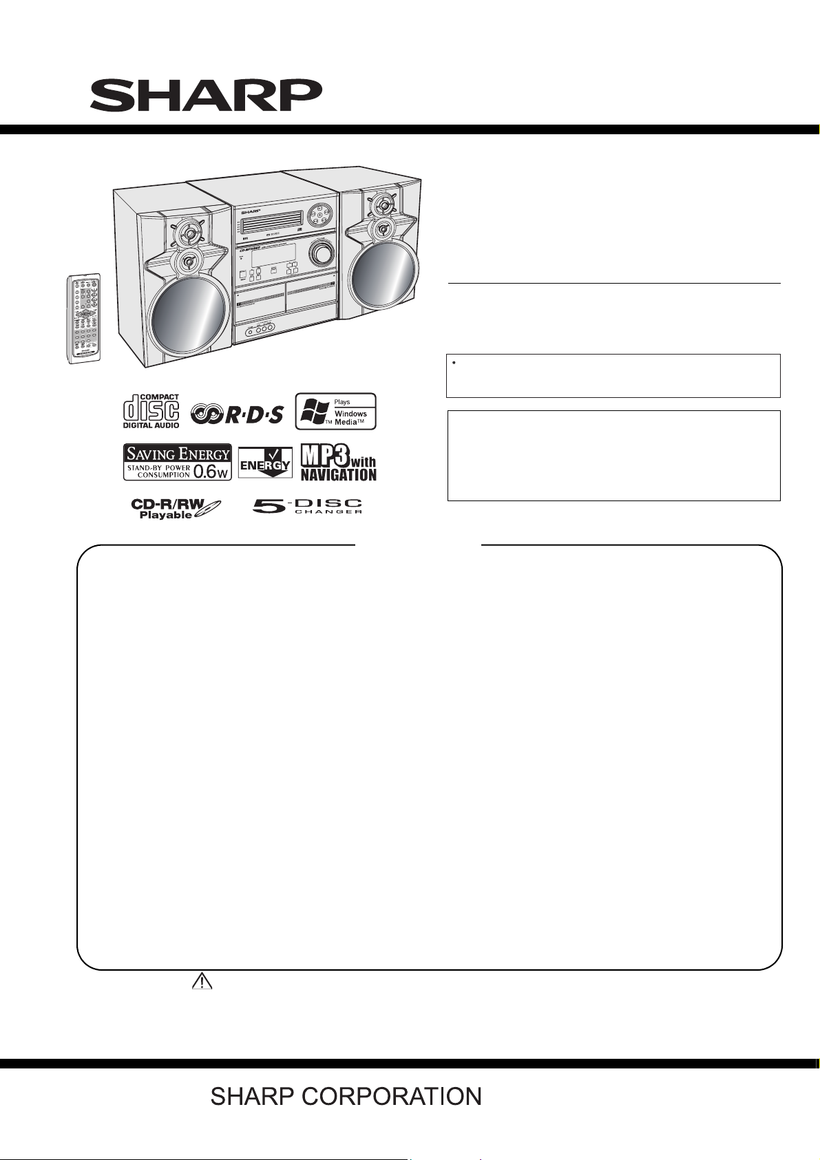
MODEL
CD-MPX860H Mini Component System consisting
of CD-MPX860H (main unit) and CP-MPX860H
(speaker system).
l
Note for users in U.K.
Recording and playback of any material may require consent
which SHARP is unable to give. Please refer particularly to the
provisions of Copyright Act 1956, the Performers Protection Acts
1963 and 1972 and subsequent statutory enactments and
orders.
CHAPTER 5. CIRCUIT DESCRIPTION
[1] Waveforms Of CD Circuit .............................. 5-1
[2] Voltage .......................................................... 5-2
CHAPTER 6. CIRCUIT SCHEMATICS AND PARTS
LAYOUT
[1] Notes On Schematic Diagram....................... 6-1
[2] Types Of Transistor And LED........................ 6-1
[3] Schematic Diagram ....................................... 6-2
[4] Wiring Side Of PWB .................................... 6-12
CHAPTER 7. FLOWCHART
[1] Troubleshooting............................................. 7-1
CHAPTER 8. OTHERS
[1] Function Table Of IC...................................... 8-1
[2] FL Display ..................................................... 8-8
[3] Wiring Of Primary Supply Leads
(for U.K. only) ................................................ 8-9
CD-MPX860H
Parts marked with " " are important for maintaining the safety of the set. Be sure to replace these parts with specified
ones for maintaining the safety and performance of the set.
Parts Guide
This document has been published to be used
for after sales service only.
The contents are subject to change without notice.
Page 2
CD-MPX860H
AudioXL-MP150Service ManualXLMP150MarketE
PRECAUTIONS FOR USING LEAD-FREE SOLDER
1. Employing lead-free solder
"MAIN, POWER, DISPLAY, JACK, CD SERVO, CD MOTOR (PWB ONLY), CD CHANGER MOTOR (PWB ONLY) "
of this model employs lead-free solder.
The LF symbol indicates lead-free solder, and is attached on the PWB and service manuals. The alphabetical character
following LF shows the type of lead-free solder.
Example:
Indicates lead-free solder of tin, silver and copper.
2. Using lead-free wire solder
When fixing the PWB soldered with the lead-free solder, apply lead-free wire solder. Repairing with conventional lead wire
solder may cause damage or accident due to cracks.
As the melting point of lead-free solder (Sn-Ag-Cu) is higher than the lead wire solder by 40 C, we recommend you to
dedicated soldering bit, if you are not familiar with how to obtain lead-free wire solder or soldering bit,
use a
service station
or service branch in your area.
3. Soldering
As the melting point of lead-free solder (Sn-Ag-Cu) is about 220 C which is higher than the conventional lead solder
by 40 C,
extended period of
of parts may be exceeded,
and as it has poor solder wettability, you may be apt to keep the soldering bit in contact with the PWB for
time. However, since the land may be peeled off or the maximum heat-resistance temperature
remove the bit from the PWB as soon as you confirm the steady soldering condition.
Lead-free solder contains more tin, and the end of the soldering bit may be easily corrected. Make sure to turn on
and off the
power of the bit as required.
If a different type of solder stays on the tip of the soldering bit, it is alloyed with lead-free solder. Clean the bit after
every use
of it.
When the tip of the soldering bit is blackened during use, file it with steel wool or fine sandpaper.
Be careful when replacing parts with polarity indication on the PWB silk.
contact our
Lead-free wire solder for servicing
Ref No.
PWB-A 92LPWB6706MANS
PWB-B 92LPWB6706DPLS
PWB-C
PWB-D
PWB-E
Parts No.
92LPWB6514CDUS
QPWBF0027AWZZ
QPWBF1055AWZZ
Description
MAIN (A1), POWER (A2)
DISPLAY (B1), JACK (B2)
CD SERVO
CD MOTOR (PWB ONLY)
CD CHANGER MOTOR (PWB ONLY)
– i –
Page 3
CD-MPX860H
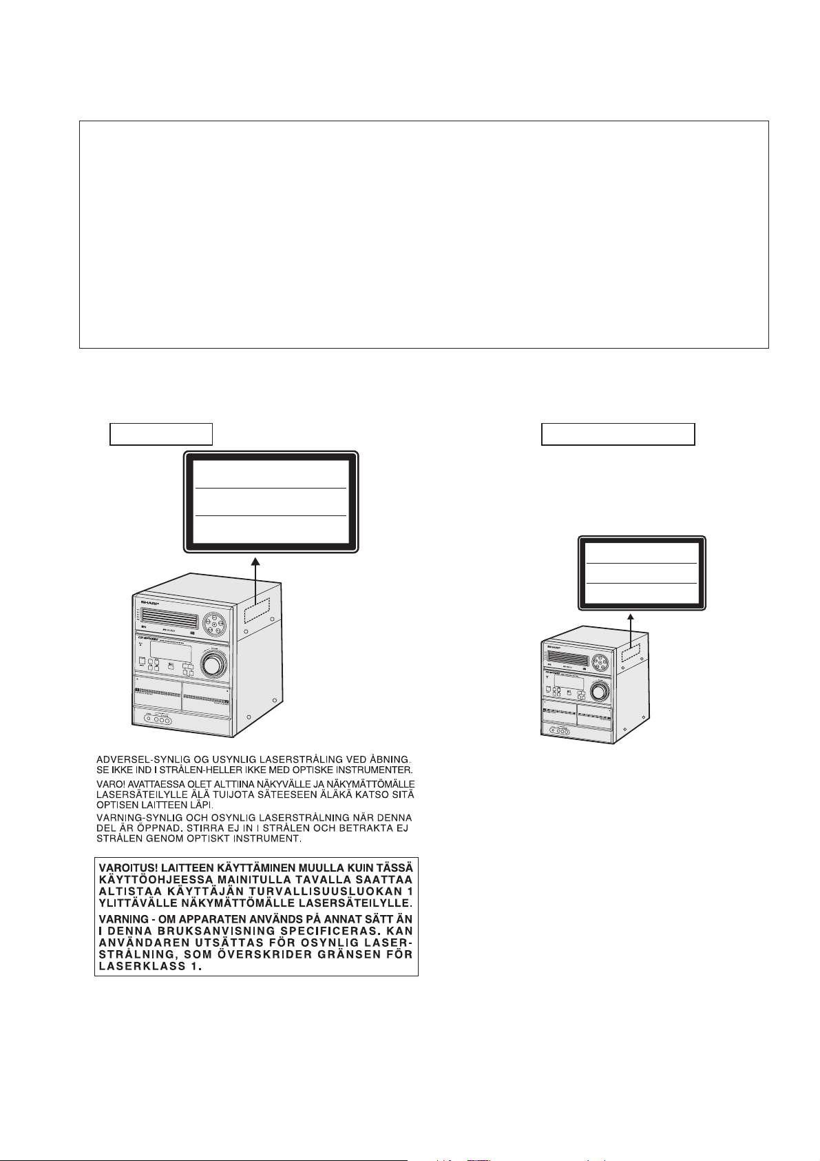
CHAPTER 1: GENERAL DESCRIPTION
[1]
Safety Precaution For Service Manual
WARNINGS
THE AEL (ACCESSIBLE EMISSION LEVEL) OF THE LASER POWER OUTPUT IS LESS THAN CLASS 1 BUT THE LASER
COMPONENT IS CAPABLE OF EMITTING RADIATION EXCEEDING THE LIMIT FOR CLASS 1. THEREFORE IT IS
IMPORTANT THAT THE FOLLOWING PRECAUTIONS ARE OBSERVED DURING SERVICING TO PROTECT YOUR EYES
AGAINST EXPOSURE TO THE LASER BEAM.
1-WHEN THE CABINET IS REMOVED,THE POWER IS TURNED ON WITHOUT A COMPACT DISC IN POSITION AND THE
PICKUP IS ON THE OUTER EDGE THE LASER WILL LIGHT FOR SEVERAL SECONDS TO DETECT A DISC. DO NOT
LOOK INTO THE PICKUP LENS.
2-THE LASER POWER OUTPUT OF THE PICKUP UNIT AND REPLACEMENT SERVICE PARTS ARE ALL FACTORY
PRESET BEFORE SHIPMENT.
DO NOT ATTEMPT TO READJUST THE LASER PICKUP UNIT DURING REPLACEMENT OR SERVICING.
3-UNDER NO CIRCUMSTANCES STARE INTO THE PICKUP LENS AT ANY TIME.
4-CAUTION-USE OF CONTROLS OR ADJUSTMENTS, OR PERFORMANCE OF PROCEDURES OTHER THAN THOSE
SPECIFIED HEREIN MAY RESULT IN HAZARDOUS RADIATION EXPOSURE.
This product is classified as a CLASS 1 LASER PRODUCT.
CD-MPX860H CD-MPX860H for U.K.
CAUTION-INVISIBLE LASER RADIATION WHEN OPEN.
DO NOT STARE INTO BEAM OR VIEW DIRECTLY WITH
OPTICAL INSTRUMENTS.
WARNUNG-UNSICHTBARE LASERSTRAHLUNG WENN GERÄT
GEÖFFNET. NICHT IN DIE STRAHLUNG SCHAUEN ODER
DIREKT MIT OPTISCHEN HILFSMITTELN BETRACHTEN.
ATTENTION-RAYON LASER INVISIBLE EN CAS D'OUVERTURE.
NE PAS REGARDER LE FAISCEAU DIRECTEMENT OU AVEC DES
INSTRUMENTS OPTIQUES.
Laser Diode Properties
Material: GaAIAs
Wavelenght: 795m
Emission Duration: continuous
Laser Output: max. 0.6 mW
1 – 1
Page 4
CD-MPX860H
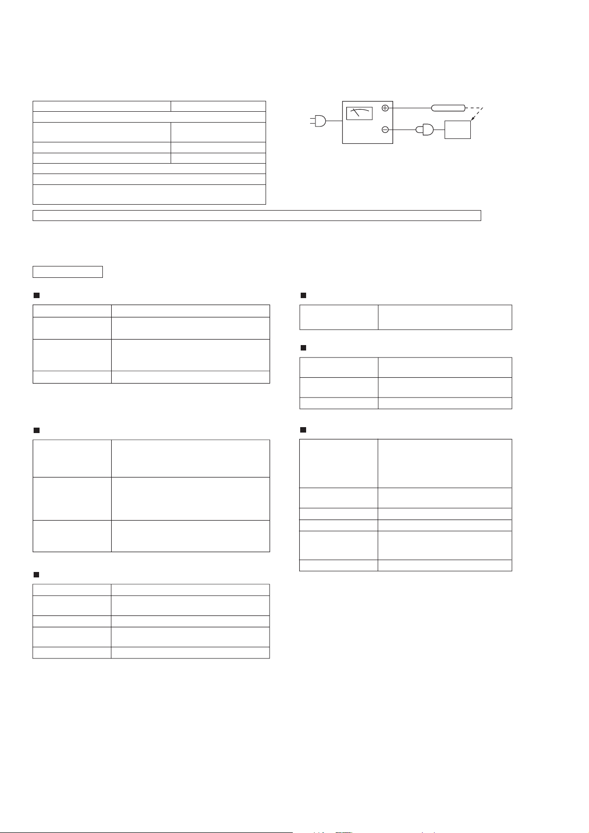
[2] Important Service Notes (For U.K. Only)
Before returning the unit to the customer after completion of a repair or adjustment it is necessary for the following withstand voltage test to be
applied to ensure the unit is safe for the customer to use.
Setting of Withstanding Voltage Tester and set.
Set name set value
Withstanding Voltage Tester
Test voltage 4,240 VPEAK
Set time 6 secs
Set current (Cutoff current) 4 mA
Unit
Judgment
OK: The “GOOD” lamp lights.
NG: The “NG” lamp lights and the buzzer sounds.
FOR A COMPLETE DESCRIPTION OF THE OPERATION OF THIS UNIT, PLEASE REFER TO THE OPERATION MANUAL.
[3]
Specifications
3,000 VRMS
CD-MPX860H
WITHSTANDING
VOLTAGE TESTER
AC
OUT
SHORT-CIRCUIT
AC POWER
SUPPLY CORD
PROBE
UNIT
CONNECT THE PROBE
TO GND OF CHASSIS
SCREW
General
Power source
Power
consumption
Dimensions
Weight
* This power consumption value is obtained when the demonstration
mode is cancelled in the power stand-by mode.
AC 230 V, 50 Hz
Power on: 105 W
Power stand-by: 0.6 W (*)
Width: 260 mm (10 - 1/4")
Height: 330 mm (13")
Depth: 323 mm (12 - 7/8")
7.5 kg (16.5 lbs.)
Amplifier
Output power
Output terminals
Input terminals
PMPO: 860 W
MPO: 430 W (215 W + 215 W) (DIN 45 324)
RMS: 240 W (120 W + 120 W) (DIN 45 324)
RMS: 160 W (80 W + 80 W) (DIN 45 500)
Speakers: 6 ohms
Headphones: 16 - 50 ohms
(recommended: 32 ohms)
Video output: 1Vp-p
Game/ Auxiliary (audio signal):
500 mV/ 47 k ohms
Game/Video: 1Vp-p
CD player
Type 5-disc multi-play compact disc player
Signal readout
D/A converter 16-bit D/A converter
Frequency
response
Dynamic range 90 dB (1 kHz)
Non-contact, 3-beam semiconductor laser
pickup
20 - 20,000 Hz
Tuner
Frequency range FM: 87.5 - 108 MHz
AM: 522 - 1,620 kHz
Cassette deck
Frequency
response
Signal/noise ratio
Wow and flutter 0.35 % (DIN 45 511)
50 - 14,000 Hz (normal tape)
55 dB (TAPE 1, playback)
50 dB (TAPE 2, recording/playback)
Speaker
Type
Maximum input
power
Rated input power
Impedance 6 ohms
Dimensions
Weight
3-way type speaker system
Super tweeter
5 cm (2") tweeter
16 cm (6 - 5/16") woofer
240 W
120 W
Width: 200 mm (7 - 7/8" )
Height: 330 mm (13" )
Depth: 231 mm (9 - 1/8")
3.3 kg (7.3 lbs.) /each
1 – 2
– 4
Page 5
CD-MPX860H for U.K.
CD-MPX860H
General
Power source AC 230 V, 50 Hz
Power
consumption
Dimensions Width: 260 mm (10 - 1/4")
Weight 7.5 kg (16.5 lbs.)
* This power consumption value is obtained when the demonstration
mode is cancelled in the power stand-by mode.
Power on: 105 W
Power stand-by: 0.6 W (*)
Height: 330 mm (13")
Depth: 323 mm (12 - 7/8")
Amplifier
Output power
Output terminals
Input terminals
RMS: 240 W (120 W + 120 W) (10% T.H.D)
RMS: 160 W (80 W + 80 W) (0.9% T.H.D)
Speakers: 6 ohms
Headphones: 16 - 50 ohms
(recommended: 32 ohms)
Video output: 1Vp-p
Game/ Auxiliary (audio signal):
500 mV/ 47 k ohms
Game/Video: 1Vp-p
CD player
Type 5-disc multi-play compact disc player
Signal readout
D/A converter
Frequency
response
Dynamic range 90 dB (1 kHz)
Non-contact, 3-beam semiconductor laser
pickup
16-bit D/A converter
20 - 20,000 Hz
Tuner
Frequency range FM: 87.5 - 108 MHz
AM: 522 - 1,620 kHz
Cassette deck
Frequency
response
Signal/noise ratio
Wow and flutter 0.3 % (WRMS)
50 - 14,000 Hz (normal tape)
55 dB (TAPE 1, playback)
50 dB (TAPE 2, recording/playback)
Speaker
Type 3-way type speaker system
Super tweeter
5 cm (2") tweeter
16 cm (6 - 5/16") woofer
Maximum input
power
Rated input power 120 W
Impedance 6 ohms
Dimensions Width: 200 mm (7 - 7/8")
Weight
240 W
Height: 330 mm (13")
Depth: 231 mm (9 - 1/8")
3.3 kg (7.3 lbs.) /each
1 – 3
–2
Page 6
CD-MPX860H
[4] Names Of Parts
12 3 45678910111213
Front panel
1. Disc Trays
2. Timer Indicator
3. Tuner (Band) Button
4. CD Button
5. ON/STAND-BY Button
6. Tape (1 2) Button
7. Game/Video Button
8. Tape 1 Cassette Compartment
9. Headphone Socket
10. Game/Video Input Sockets
11. Disc Tray Open/Close Button
12. Disc Number Select Buttons
13. Volume Control
14. CD or Tape Stop Button
15. CD Play or Repeat, Tape Play Button
16. CD Track Up or Fast Forward, Tape 2 Fast Forward,
Tuner Preset Up, Time Up Button
17. CD Track Down or Fast Reverse, Tape 2 Rewind,
Tuner Preset Down, Time Down Button
18. Tape 2 Cassette Compartment
19. Remote Sensor
Display
1. Disc Number Indicators
2. MP3/WMA Folder Indicator
3. MP3/WMA Title Indicators
4. MP3 Indicator
20 21
22
23
14
15 1617
18
19
3
4
5
5. WMA Indicator
6. RDS Indicator
7. Traffic Announcement Indicator
8. Dynamic PTY Indicator
9. Traffic Programme Indicator
10. Sleep Indicator
11. Timer Play Indicator
12. Timer Recording Indicator
13. Tape 2 Record Indicator
14. MP3/WMA Total Indicator
15. Daily Timer Indicator
16. FM Stereo Mode Indicator
17. FM Stereo Receiving Indicator
18. Tape Play Indicator
19. Memory Indicator
20. Extra Bass Indicator
21. Disc Repeat Play Indicator
22. Disc Pause Indicator
23. Disc Play Indicator
6
Rear panel
1
7
2
1. Cooling Fan
2. AC Power Lead
3. FM 75 Ohms Aerial Socket
4. AM Aerial Earth Terminal
5. AM Loop Aerial Terminal
6. Video out Socket
7. Front Speaker Terminals
11
2
4
3
5
Front Speaker
1. Tweeter
2. Super Tweeter
3. Woofer
4. Bass Reflex Duct
5. Speaker Wire
1 – 4
– 4
Page 7
CD-MPX860H
1
13
14
8
15
9
10
2
11
12
3
4
16
22
24
26 27 28 29
17
18
19
20
21
23
25
5
6
7
30 31 32
Remote control
1. Remote Control Transmitter
2. Disc Number Select Buttons
3. Clock/Timer Button
4. Character Input/Disc Direct Search Buttons
5. Equaliser Mode Select Button
6. Extra Bass/Demo Button
7. Volume Up and Down Buttons
8. ON/STAND-BY Button
9. CD Button
10. Tuner (Band) Button
11. Tape (1 2) Button
12. Game/Video Button
13. Disc Clear/Dimmer Button
14. Disc Random Button
15. Disc Stop Button
16. Tape Stop Button
17. Memory Button
18. Disc Pause Button
19. Disc Play or Repeat Button
20. Tape Play Button
21. Tape 2 Record Pause Button
22. Tuning Up, Cursor Up Button
23. Disc Track Up or Fast Forward, Tape 2 Fast Forward,
Tuner Preset Up, Time Up, Cursor Right Button
24. Disc Track Down or Fast Reverse, Tape 2 Rewind,
Tuner Preset Down, Time Down, Cursor Left Button
25. Tuning Down, Cursor Down Button
26. MP3/WMA Navigation Mode Select Button
27. Character Button
28. MP3/WMA Display Button
29. Enter Button
30. RDS ASPM Button
31. RDS PTY Button
32. RDS Display Button
1 – 5
–2
Page 8
CD-MPX860H
CD-ES700/CD-ES77CD-ES700/CD-ES77Service ManualCD-ES700/CD-ES77MarketE
CHAPTER 2. ADJUSTMENTS
[1] Mechanism Section
• Driving Force Check
Torque Meter Specified Value
Play: TW-2111 Tape 1: Over 80 g
• Torque Check
Torque Meter Specified Value
Play: TW-2111 30 to 80 g.cm 30 to 80 g.cm
Fast forward: TW-2231 — 70 to 180 g.cm
• Tape Speed
Tape 2: Over 80 g
Tape 1 Tape 2
— 70 to 180 g.cm
Normal
speed
Test Tape Adjusting
Point
MTT-111 Variable
Resistor in
motor.
TAPE MECHANISM
Ta pe
Motor
Figure 1
Specified
Value
3,000 ± 30 Hz
Speaker
Variable Resistor in motor
Instrument
Connection
Speaker
Terminal (Load
resistance:
6 ohms)
2 – 1
Page 9
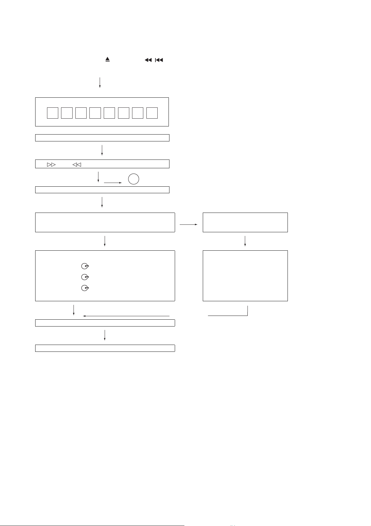
[2] Test Mode
• Setting the test mode
During stand-by mode, press GAME/VIDEO button
while pressing down the button and button.
then, press the CD button to enter the test mode.
CD-MPX860H
C D T E S T
OPEN/CLOSE operation is using manual. IL isn’t done
<< >>,<< >>buttons make pick's slide possible.
to page 2-3
<<PLAY>> key input.
Do TOC IL. Do normal play.
When these following key is input into PLAY key, track number can be appoint directly.
<< 1>> key: Track 4
<< 2>> key: Track 9
<< 3>> key: Track 15
A
IL isn’t done
IL isn’t done
<<MEMORY>>
key input.
Adjustment result automatically will
display as below for each 2 sec:
a) "FOF_XXXX"
b) "TOF_XXXX"
c) "TBAL_XX"
d) "TGAN_XX"
f) "FGAN_XX"
g) "RFLS_XX"
<<STOP>> key input.
STOP
explanation:
a) Focus off set = "FOF_XXXX"
b) Tracking off set = "TOF_XXXX"
c) Tracking balance = "TBAL_XX"
d) Tracking Gain = "TGAN_XX"
f) Focus Gain = "FGAN_XX"
g) RF level shift = "RFLS_XX"
VOL — Last memory
P. G E Q — FL AT
X-BASS — OFF
To cancel : Power OFF
––––––––
2 – 2
Page 10
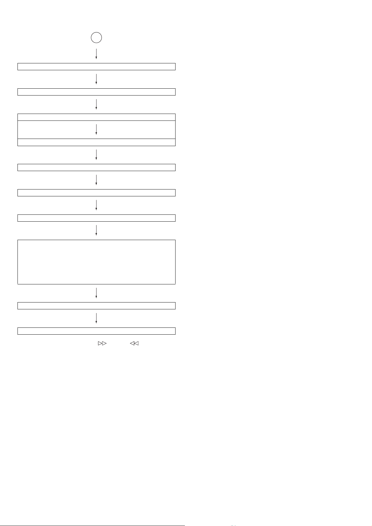
CD-MPX860H
Tracking OFF play at that specific point.
Tracking ON play from that specific point.
A
<<MEMORY>> key input.
Laser ON.
<<MEMORY>> key input.
<<MEMORY>> key input.
<<MEMORY>> key input.
Adjustment result automatically will display as below for each 2 sec :
a) "FOF_XXXX"
b) "TOF_XXXX"
c) "TBAL_XX"
d) "TGAN_XX"
f) "FGAN_XX"
g) "RFLS_XX"
<<STOP>> key input.
STOP
Sliding the PICKUP with<< >>, << >> button
must only be in STOP mode.
explanation:
a) Focus off set = "FOF_XXXX"
b) Tracking off set = "TOF_XXXX"
c) Tracking balance = "TBAL_XX"
d) Tracking Gain = "TGAN_XX"
f) Focus Gain = "FGAN_XX"
g) RF level shift = "RFLS_XX"
VOL — Last memory
P. G E Q — FL AT
X-BASS — OFF
To cancel : Power OFF
2 – 3
Page 11
CD-MPX860H
[3] CD Section
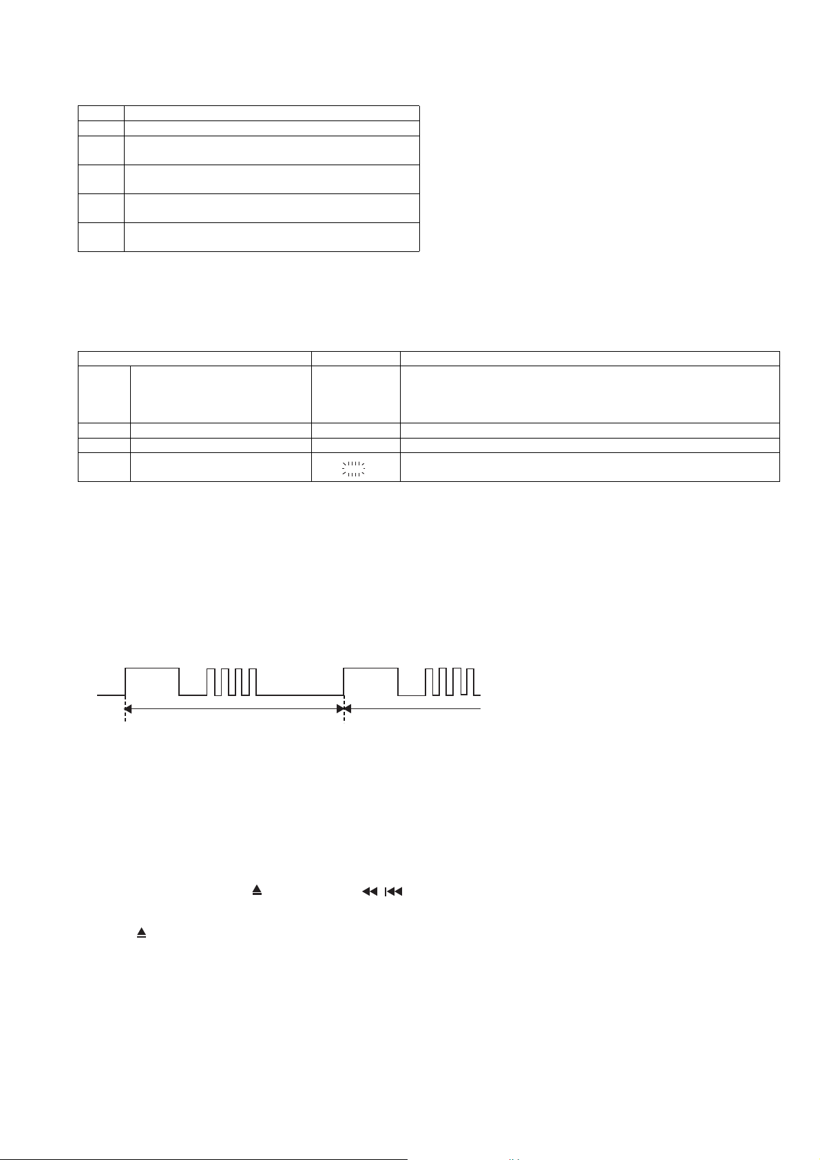
CD Error code description
Error Explanation
10* CAM error. Can't detect CAM switch when CAM is moving.
11* When it detect cam operation error during initialize
process.
20* TRAY error. Can't detect TRAY switch when TRAY is
moving.
21* When it detect TRAY operation error during initialize
process.
31 When it change to CD function, DSP cannot read initial
data.
* 'CHECKING'
If Error is detected, 'CHECKING' will be displayed instead of 'ER-CD**'. 'ER-CD**' display will only be displayed
when error had been detected for the 5
Standard Specification of Stereo System Error Message Display Contents
Error Contents Display Notes
CD CD Changer Mechanism Error. 'ER-CD**' (*) 10: CAM SW Detection NG during normal operation.
CD DSP Communication Error. 'ER-CD31' DSP COMMUNICATION ERROR.
Focus Not Match/IL Time Over. 'NO DISC'
TUNER PLL Unlock. PLL Unlock.
th
times.
FM 87.5 MHz
11: CAM SW Detection NG during initialize process.
20:TRAY SW Detection NG during normal operation.
21:TRAY SW Detection NG during initialize process.
(*) CHECKING:
If CD changer mechanism error is detected, 'CHECKING' will be display instead of 'ER-CD**'. 'ER-CD**' display will
only be display when error had been detected for the 5
th
times.
Speaker abnormal detection and +B PROTECTION display
In case speaker abnormal detection or +B PROTECTION had occurred, the unit will automatically enter to stand - by
mode and Timer indicator will be flashing as below.
Example : In case of speaker abnormal
TIMER
LED
ON
OFF
NO. 1
NO.1 : +B Protection
NO.2 : Speaker abnormal
OFF
FLASHING
NO. 2
1 FRAME
OFF
ON
NO. 1
FLASHING
OFF
NO. 2
(REPEAT)
+B PROTECTION is condition when irregular process occur on power supply line.
BEFORE TRANSPORTING THE UNIT
The following process need to be taken after set tapering/parts replacement.
1. Press the ON/STAND-BY button to enter stand-by mode.
2. While pressing down the button and the button, press the GAME/VIDEO button. The Micro Computer
version number will be displayed as "CM*****".
3. Press button until "WAIT"→ "FINISHED" appears.
4. Unplug the AC cord and the unit is ready for transporting.
2 – 4
Page 12
CD-MPX860H
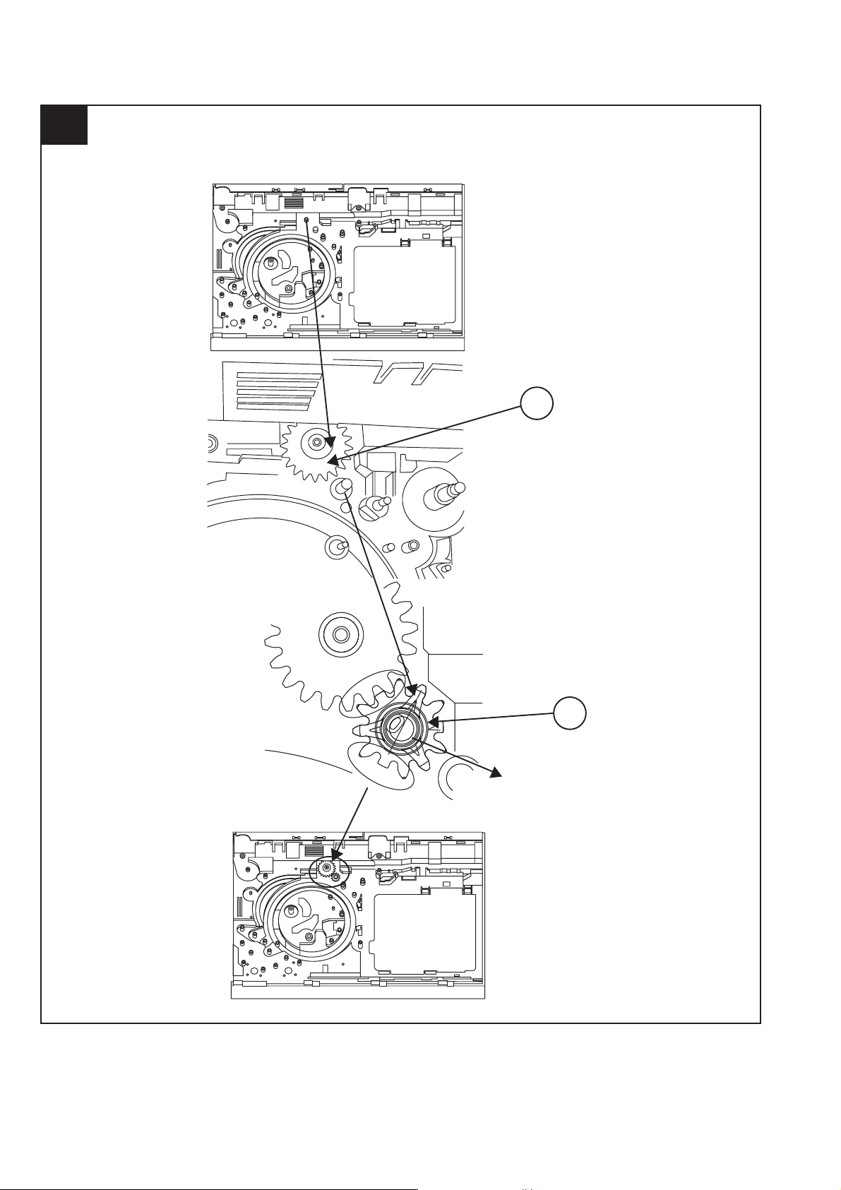
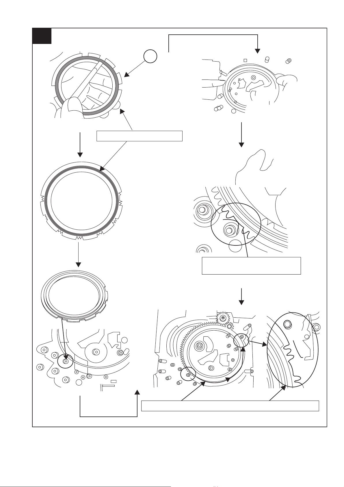
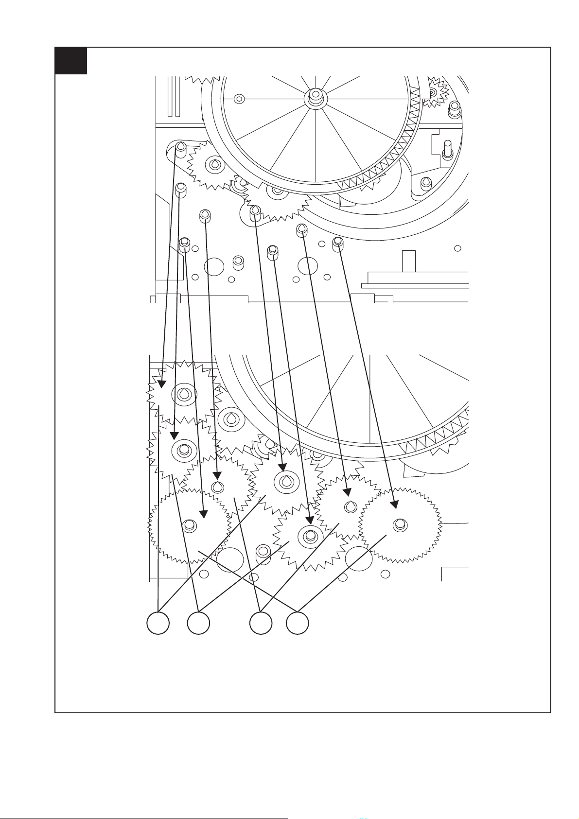
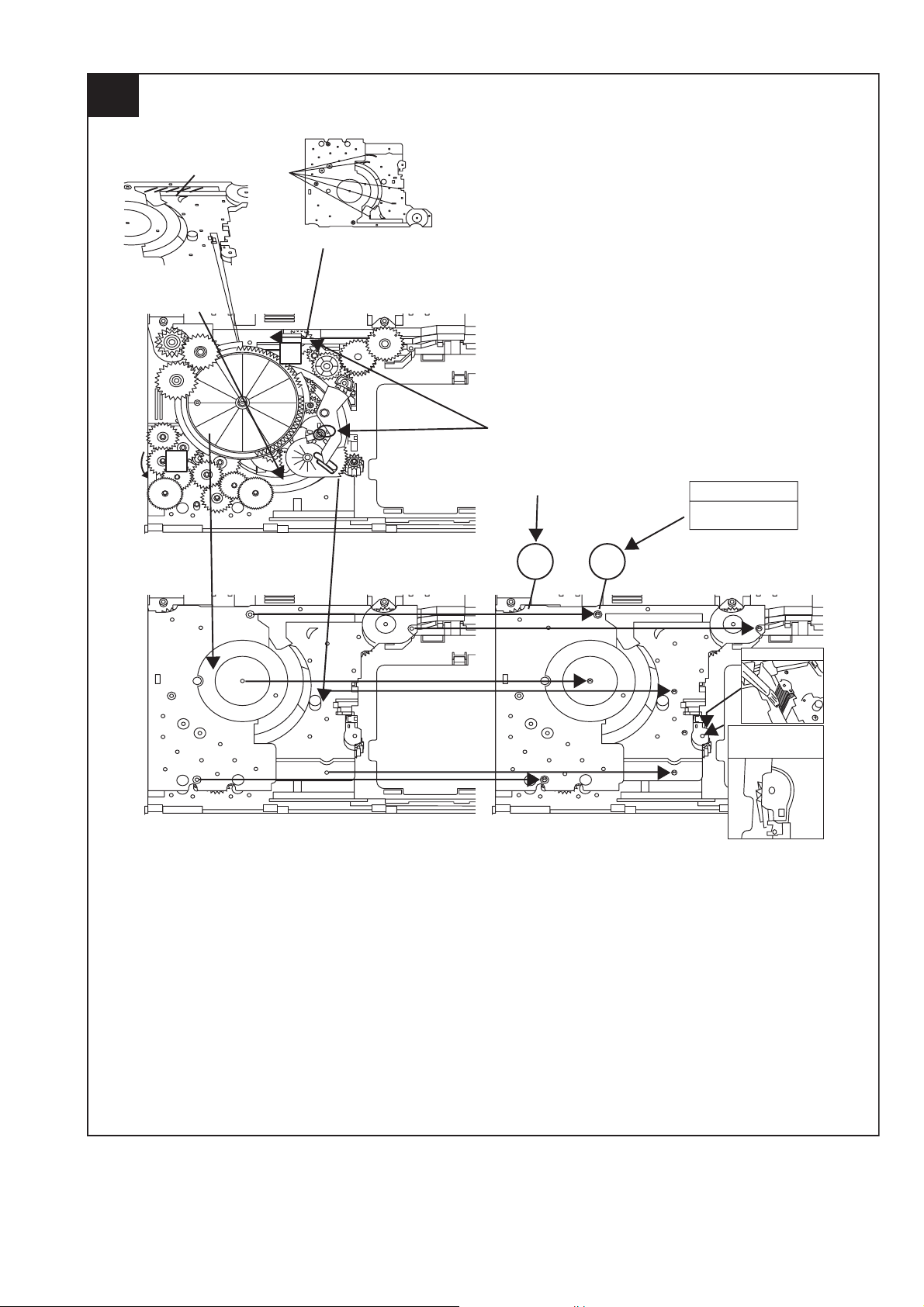
[4] CD Changer Mechanism Section
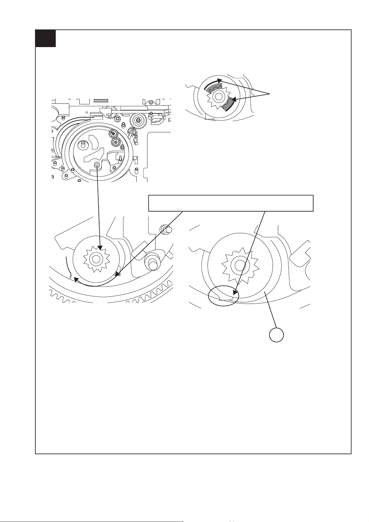
• All numbers in the drawing correspond to those in parts guide (CHANGER MECHANISM PARTS).
1
141
140
HALF GEAR
MUST BE ARRANGED AS SHOWN
2 – 5
Page 13
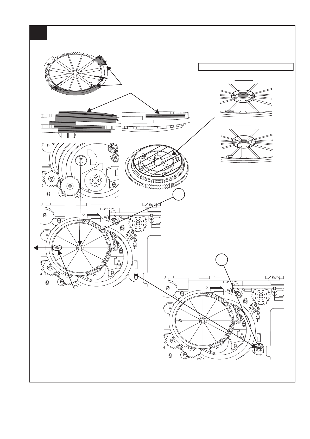
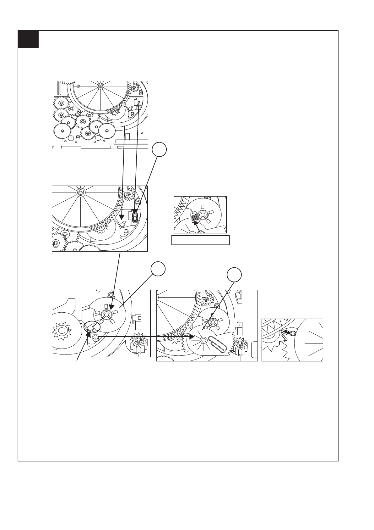
2
CD-MPX860H
139
APPLY SANKOL SHS1001 BEFORE FIX
FIX ITEM 139 ACCORDING TO THE
PICTURE AS SHOWN ABOVE
ROTATE MODE BIG GEAR UNTIL REACH AS SHOWN IN PICTURE
2 – 6
Page 14
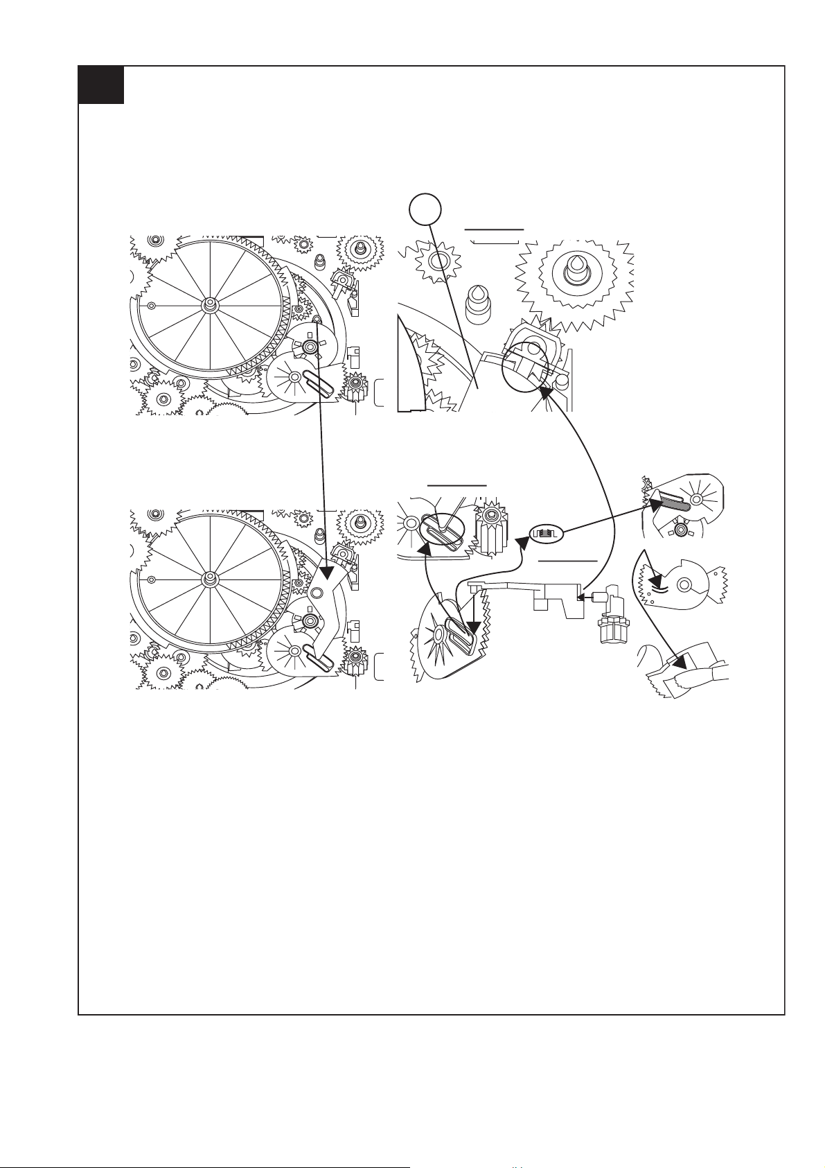
CD-MPX860H
3
143
APPLY GREASE SC141
112
PULL THE LEVER UNITIL
REACH THE ARROW MARK
2 – 7
Page 15
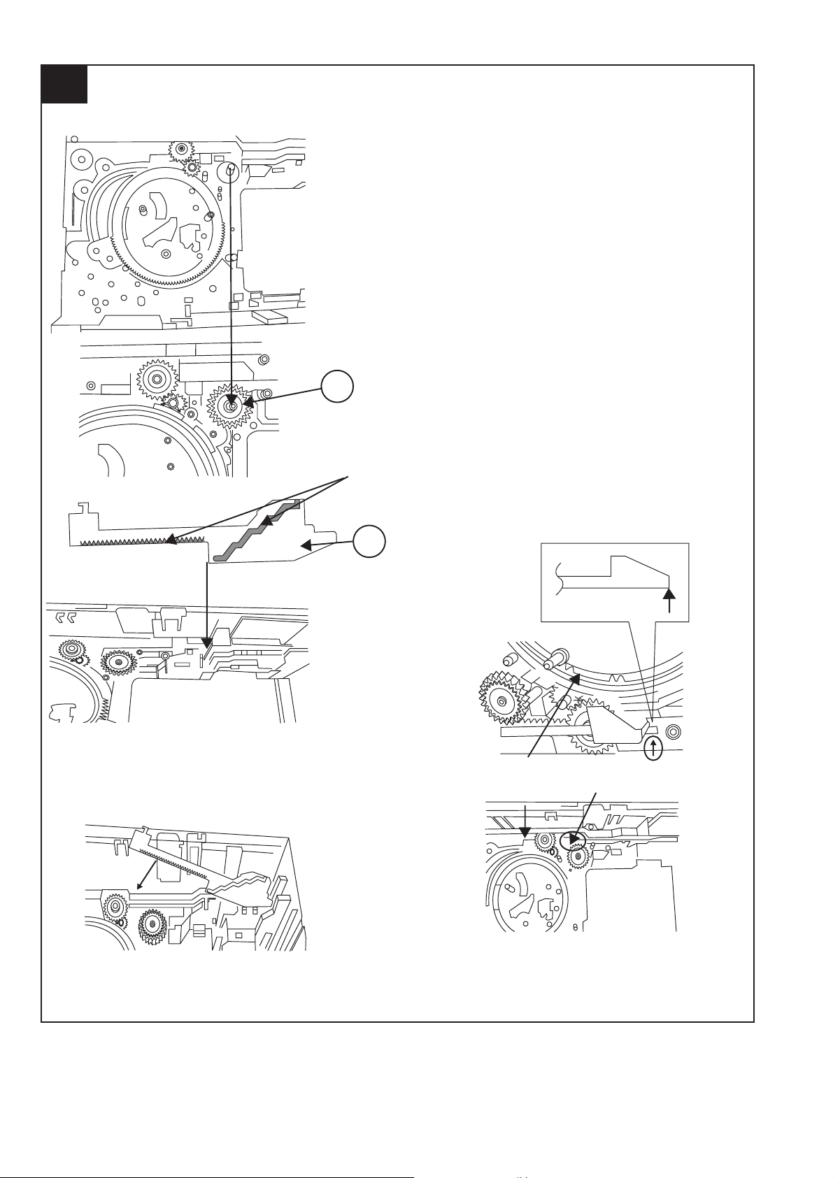
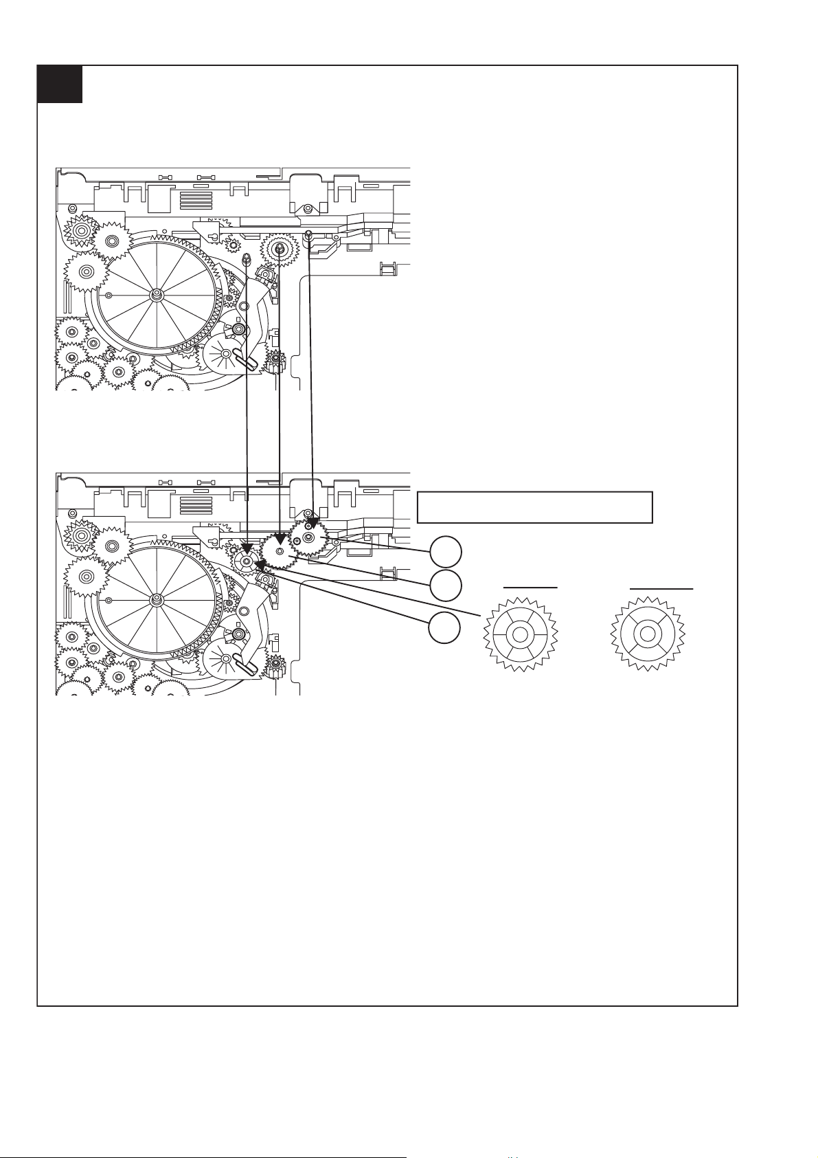
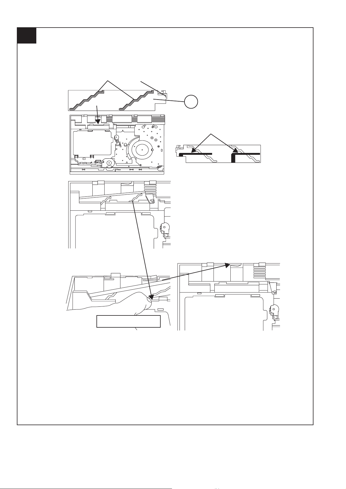
4
CD-MPX860H
FIGURE 2
FIGURE 1
152
142
APPLY GREASE SC141
118
SLOT CLAMP
SWITCH ARM INSIDE BASE SLOT
HALF GEAR MUST BE
ARRANGED AS SHOWN
2 – 8
Page 16
CD-MPX860H
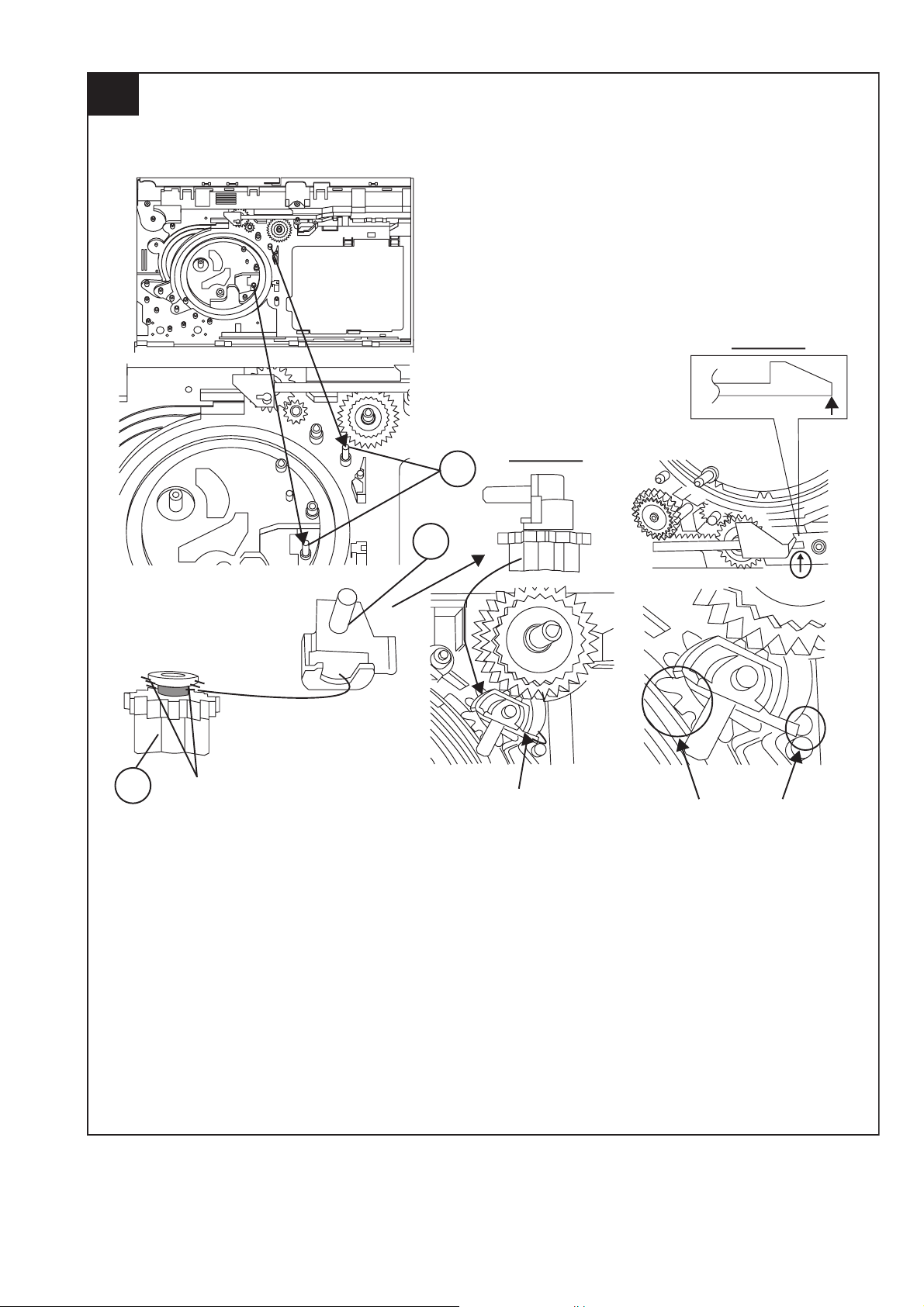
5
APPLY GREASE SC141 AT BOTTOM SIDE
OF GEAR FOLLOW MARKING (REFER TO GRAY AREA)
NO NEED TO APPLY GREASE AT BOTTOM
SIDE
FIGURE 1
APPLY GREASE SC141
AT TOP SIDE OF GEAR
FOLLOW MARKING
(REFER TO GRAY AREA)
127
IF DIRECTION IS OTHER THAN DIRECTION
SHOWN IN FIGURE 1, IT IS INCORRECT
CORRECT
128
INCORRECT
BLACK MARK
2 – 9
Page 17
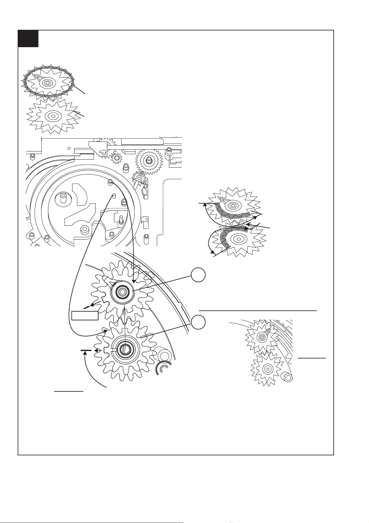
6
CD-MPX860H
APPLY GREASE SC141 AT
HALF GEAR AREA
ROTATE CLOCKWISE UNTIL REACH HERE (MAXIMUM)
129
2 – 10
Page 18
CD-MPX860H
7
151150149
2 – 11
Page 19
8
CD-MPX860H
THE SHOWN AREA MUST FREE FROM GREASE
CORRECT
GREASE SC141 APPLICATION LENGTH
GREASE APPLICATION PORTION
INCORRECT
SHOWN HOLE MUST FACING ARROW DIRECTION
124
131
2 – 12
Page 20
CD-MPX860H
9
138 126 125
APPLY GREASE SC141
AT BOTTOM SIDE
ONLY
TR-RE JOINT GEAR C
APPLY GREASE SC141 ONLY AT TOP SIDE GEAR
MUST BE FIXED ACCORDINGLY TO
THE HOLE'S
2 – 13
Page 21
10
CD-MPX860H
148 147 146 145
2 – 14
Page 22
CD-MPX860H
11
121
144
WHEN FIXING ITEM 144 MUST FOLLOW AS SHOWN
APPLY GREASE SC141
130
2 – 15
Page 23
12
CD-MPX860H
117
FIGURE 2
FIGURE 1
APPLY GREASE
SC141
FIGURE 3
APPLY GREASE SC141
2 – 16
Page 24
CD-MPX860H
13
ITEM 133 , 134 MUST APPLY GREASE SC141
ON TOP SIDE GEAR ONLY
134
GEAR 112 GEAR 112
133
132
CORRECT
TOP VIEW AFTER
BEING ASSEMBLED
INCORRECT
IT IS INCORRECT TO
FIX IT IN REVERSED
DIRECTION
2 – 17
Page 25
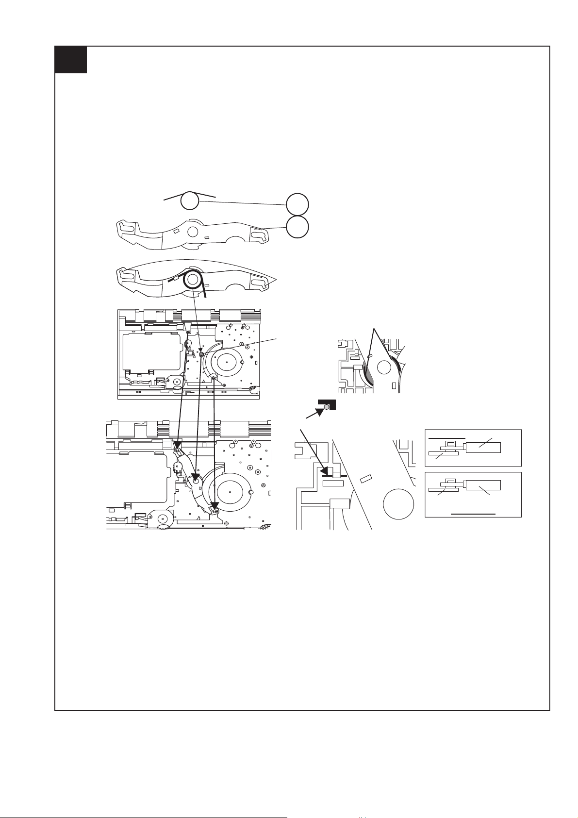
14
APPLY GREASE SC141
BEFORE FIX
MOVE 112 UNTIL TOUCH THE WALL
A
CD-MPX860H
B
DURING GEAR A ROTATE
MUST PRESS SHOWN AREA
AND LEVER B WILL MOVE
ARROW DIRECTION THEN
FIX PART 108
SCREW TORQUE
+0.5
2 kgf-cm
- 0
108 803 x6
APPLY GREASE SC141
CONFIRM WHETHER
FIXED
PROPELY OR NOT
2 – 18
Page 26
CD-MPX860H
15
APPLY GREASE SC141
113
BEHIND THE LEVER NEED TO APPLY GREASE SC141
PULL IT THEN LEVER WILL
MOVE IN
2 – 19
Page 27
16
CD-MPX860H
123
115
APPLY GREASE SC141
APPLY GREASE SC141 BEFORE FIX
APPLY GREASE
SC141 AT BOSS
SPRING MUST BE ARRANGED UNDER THE HOOK
CORRECT LR JOINT LEV
BOARD R
BOARD R
LR JOINT LEV
INCORRECT
2 – 20
Page 28
CD-MPX860H
17
IT IS INCORRECT IF ASSEMBLED IN
A REVERSED DIRECTION
103 137 136
APPLY GREASE SC141
BIG SLOT MUST FACING OUT
WHEN FIX AND AFTER FIXED TO BASE CHASSIS.
AFTER ASSEMBLY, CONFIRM WITH FREE DROP TEST
GEAR POSITION DURING FIXING
2 – 21
Page 29
18
CD-MPX860H
IT IS INCORRECT IF ASSEMBLED IN
A REVERSED DIRECTION
APPLY GREASE SC141
104
135
136
BIG SLOT MUST FACING OUT
WHEN FIX AND AFTER FIXED TO BASE CHASSIS
AFTER ASSEMBLY, CONFIRM WITH FREE DROP TEST
GEAR POSITION DURING FIXING
CONFIRM BOTH GEARS SIT PROPERLY AND LOCKED
2 – 22
Page 30
CD-MPX860H
19
120
AFTER FIX OUTER UP/DOWN LEVER HOLD AS SHOWN PORTION AND
MOVE UP/DOWN THEN CONFIRM WHETHER LEVER GO INSIDE THE HOLE OR NOT
137
IT IS CORRECT IF THE LEVER HOLD
BIGGER SLOT FACING OUT
ENTERS THE HOLE
119
IT IS INCORRECT IF THE LEVER HOLD DOES NOT
ENTER THE HOLE
135
BIGGER SLOT FACING OUT
ALL OF THIS 135 AND 137 GEAR FIX TOGETHER WITH 119
AND 120 LEVER ( MOVE TOGETHER )
2 – 23
Page 31

20
CD-MPX860H
BIG SLOT FACING OUT
110
2 – 24
Page 32

CD-MPX860H
21
PUSH THE LEVER ACCORDING TO ARROW
DIRECTION THEN FIX
WHEN FIXING MAIN BASE ASSEMBLY FOLLOW ACCORDING TO PICTURE 1
PICTURE 1
CORRECT INCORRECT INCORRECT
MAKE SURE MECHA HOLDER SHAFT FIX PROPERLY TO LEVER
PICTURE 3
PICTURE 2
2 – 25
Page 33

22
APPLY SANKOL (SHS1001)
101
102
APPLY SANKOL
(SHS1001) ON TOP
CD-MPX860H
APPLY SANKOL (SHS1001) INSIDE
THE SLOT & OTHER SHOWN PORTION
APPLY SANKOL
(SHS1001)
APPLY SANKOL (SHS1001) AT
TRAY SLIDING PORTION
FIX TRAY NO 1 FIRST THAN
FOLLOW OTHER
APPLY SANKOL (SHS1001) AT BACK PORTION
COSMO GUIDE TRAY HAVE
MARKING AS SHOWN
2 – 26
Page 34

CD-MPX860H
23
GEAR UP/DOWN BOARD
111
APPLY GREASE SC141 AT INNER & OUTER GEAR SLIDING PORTION
WHEN FIX GEAR UP/
DOWN BOARD THE
TWO LEVER MUST AT
PARALLEL LINE AND
POSITIONED AT TOP
MAX SIDE
AFTER ASSEMBLY GEAR UP/DOWN BOARD
2 – 27
Page 35

24
CD-MPX860H
SCREW TORQUE
+0.5
3 kgf-cm
- 0
ROTATE THE GEAR TO MOVE UP 111 GEAR
UP AND DOWN BOARD BEFORE SCREW
804
2 – 28
Page 36

CD-MPX860H
25
AFTER ASSEMBLY TOP PLATE
FIX THE FFC
FFC4
AFTER PUSH, MAKE SURE SNAP PROPERLY
PRESS IN
AFTER FIX, PUSH FOLLOW ARROW DIRECTION
BEFORE LOCK
AFTER LOCK
BACK
PORTION
107
122
BEFORE LOCK
SLOT IN
BEFORE LOCK
AFTER LOCK
AFTER LOCK
MUST CONFIRM
MUST CONFIRM
2 – 29
Page 37

26
CORRECT
INCORRECT
CD-MPX860H
CAUTION
1. MAKE SURE NO PWB CHIP INSIDE SET .( BEFORE FIX MAKE
SURE PWB IS FREE FROM DUST , GREASE & ETC )
803
2 – 30
Page 38

CD-MPX860H
27
APPLY GREASE SC141
THE TWO SLOT MUST FREE
FROM GREASE SC141
APPLY GREASE SC141
BELOW THE MARKING
FOR BOTH PORTION
ASSEMBLY SEQUENCE
1. APPLY GREASE SC141 TO MAIN BASE
GREASE SC141 APPLICATION AREA
ALL BOSS
APPLY GREASE
SC141
CAUTION
TRAY SLIDING
AREA MUST
FREE FROM
GREASE SC141
APPLY GREASE
SC141
APPLY GREASE
APPLY GREASE SC141 AT WALL
APPLY GREASE
SC141
SC141
105
APPLY GREASE SC141
AT BOTH SLOT
APPLY GREASE SC141 AT 3 HALF MOON
1 RIB ONLY
APPLY GREASE
SC141
APPLY GREASE SC141
INSIDE SLOT
2 – 31
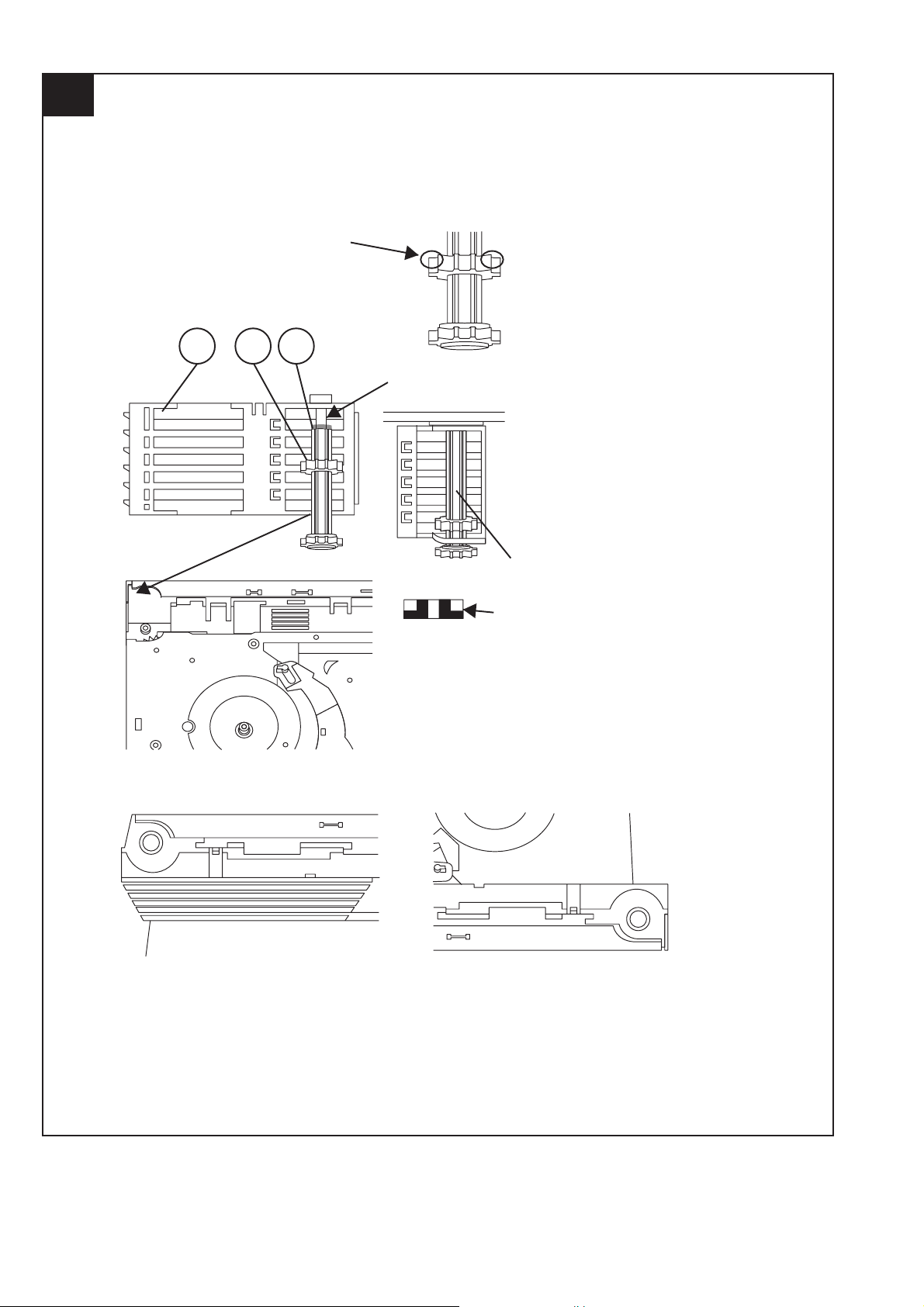
Page 39

28
REFERENCE ONLY
MOTOR GEAR HEIGHT FROM
MAIN BASE 12.2
+
0.1
-
0.1
-
+
12.2
CD-MPX860H
MOTOR SCREWING HOLE
MUST HAVE GAP
M1,2
801
-0
13.8 + 0.2
APPLY GREASE SC141
SCREW TORQUE
1.5 + 0.5
-0
AFTER SCREW MOTOR, CONFIRM THE
ARRANGEMENT AS IN FIGURE 2
FIGURE 2
2 – 32
Page 40

CD-MPX860H
29
APPLY SANKOL (SHS1001)
3.1 + 0.1
SHAFT X 3 DIM AFTER INSERTION
MUST CONFIRM EVERYDAY
109-2
APPLY GREASE AT THE SLIDING PORTION
114
116
UP / DOWN
HOLDER CHANGE
TO NATURE
COLOR
SANKOL
APPLICATION AREA
(SHS1001)
APPLY GREASE SC141
2 – 33
Page 41

30
CD-MPX860H
BEFORE MELT IT
AFTER MELT IT ( MUST FLAT )
WHEN FITTING STABILIZER PLATE TO STABILIZER,
ROTATE STABILIZER ANTI CLOCKWISE BY JIG
( STRICTLY CANNOT FIT USING HAND)
( BY HAND CANNOT X )
BELOW
AFTER ASSEMBLED TO
HOLDER, STABILIZER
NEED TO BE CLEANED
WITH ALCOHOL DISC
TOUCHING SURFACE
2 – 34
Page 42

CD-MPX860H
31
106
APPLY GREASE SC141
MUST MAKE SURE SNAP PROPERLY BOTH SIDE
ALL SURFACE MUST TOUCH
CORRECT INCORRECT
GAP
INCORRECT
2 – 35
Page 43

32
CD-MPX860H
NO GAP HAVE GAP
CORRECT INCORRECT
2 – 36
Page 44

CD-MPX860H
CD-ES700/CD-ES77CD-ES700/CD-ES77Service ManualCD-ES700/CD-ES77MarketE
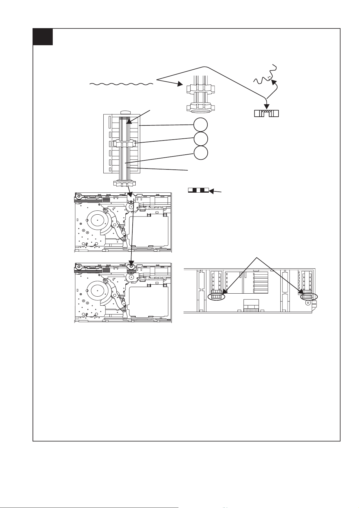
CHAPTER 3. MECHANISM BLOCKS
[1] Caution On Disassembly
Follow the below-mentioned notes when disassembling the unit and reassembling it, to keep it safe and ensure
excellent performance:
1. Take cassette tape and compact disc out of the unit.
2. Be sure to remove the power supply plug from the wall outlet before starting to disassemble the unit.
3. Take off nylon bands or wire holders where they need to be removed when disassembling the unit. After servicing
the unit, be sure to rearrange the leads where they were before disassembling.
STEP REMOVAL PROCEDURE FIGURE
1 Top Cabinet 1
2 Side Panel
1. Screw ..................... (A1) X 5
1. Screw ..................... (B1) X 8
1
(Left/Right)
3 CD Changer unit
1. Hook ....................... (C1) X 2
2
2. Socket .................... (C2) X 1
3. Flat Cable ............... (C3) X 1
4 Rear Panel with
1. Screw .....................(D1) X 9
2
Fan motor
5 Front Panel
1. Screw ..................... (E1) X 3
2. Flat Cable ............... (E2) X 1
3. Socket .................... (E3) X 1
4. Hook ....................... (E4) X 2
6 Main PWB 2,3
1. Screw ..................... (F1) X 3
2. Socket .................... (F2) X 4
7 Power PWB 3
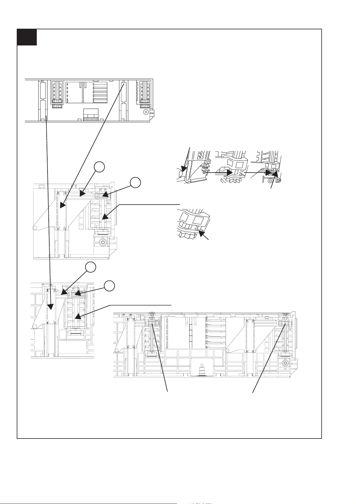
8 Tape Mechanism 4
1. Screw .....................(G1) X 4
1. Screw .....................(H1) X 6
2,3
2
2
3
3
2. Flat Cable ............... (H2) X 1
9 Game Input PWB 5
10 Display PWB
1. Screw ......................(J1) X 2
1. Knob ....................... (K1) X 1
5
2. Nut.......................... (K2) X 1
3. Washer................... (K3) X 1
4. Screw ..................... (K4) X 6
11 CD Servo PWB 6
1. Screw ......................(L1) X 3
2. Flat Cable ................(L2) X 2
3. Socket .....................(L3) X 1
12
Changer
Mechanism Unit
15 CD Mechanism 8
1. Screw .....................(M1) X 4
2. Changer Chassis....(M2) X 1
1. Screw .....................(N1) X 4
7
Note:
After removing the connector for the optical pickup from the
connector, wrap the conductive aluminium foil around the front end
of the connector so as to protect the optical pickup from electrostatic damage.
Top Cabinet
Front Panel
CD Changer
Unit
Rear Panel
(D1)x9
3x10mm
O
Figure 2
CD Servo PWB
Fan Motor
PULL
Hook
(C1)x1
(E3)x1
Power PWB
(F2)x1
(C3) x1
(F3)x1
(F2)x2
(C2) x1
Main PWB
(F1)x1
3x10mm
O
Front Panel
(E2)x1
PULL
Lug wire
(E1)x1
3x10mm
O
Hook
(C1)x1
(A1)x2
3x12mm
(B1)x2
3x10mm
(A1)x1
3x12mm
Side Panel
(Right)
(B1)x2
3x10mm
Figure 1
Rear Panel
(B1)x2
3x10mm
(B1)x2
3x10mm
(A1)x2
3x12mm
Side Panel
(Left)
Power PWB
Figure 3
3 – 1
(E4)x1
PULL
O
(G1)x4
4x8mm
(F2)x1
(F1)x2
3x6mm
O
(E1)x2
3x8mm
O
Front Panel
Hoo k
(E4)x1
PULL
Page 45

Tape
O
Mechanism
(H1)x6
3x10mm
Figure 4
(H2)x1
Lug wire
Front Panel
(M1)x4
3x10mm
CD-MPX860H
(M2)x1
(K4)x6
2.6x10mm
Figure 5
(L2)x1
(J1)x2
Special
(L1)x3
3x10mm
(L3)x1
Front Panel
Display PWB
(L2)x1
Nut (K2)x1
(K1)x1
Washer
(K3)x1
Game Input
PWB
(N1)x4
2.6x10mm
CD Mechanism
Figure 7
Figure 8
Changer
Mechanism
Unit
Changer
Mechanism
Unit
CD Servo
PWB
Figure 6
Changer
Mechanism
Unit
3 – 2
Page 46

CD-MPX860H
STEP REMOVAL PROCEDURE FIGURE
1 Woofer 1. Front Panel............................. (A1) x1 9
2. Screw .....................................(A2) x4
2 Tweeter 1. Screw .....................................(B1) x2
3 Super tweeter
1. Screw .....................................(C1) x2
Speaker Box
Front Panel
(A1)x1
3x10mm
O
WOOFER
(B1)x2
O
3x10mm
TWEETER
SUPER TWEETER
(C1)x2
(A2)x4
4x16mm
O
Screwdriver
Figure 9
3 – 3
Page 47

[2] Removing And Reinstalling The Main Parts
1. TAPE MECHANISM SECTION
Perform steps 1 to 5 and 6 of the disassembly method
to remove the tape mechanism.
1.1. How to remove the record/playback and erase
heads (TAPE 2) (See Fig. 1)
1. When you remove the screws (A1) x 2 pcs., the
recording/playback head and three-dimensional
head of the erasing head can be removed.
TAP E 2
Clutch Ass'y
Record/Playback
Head
CD-MPX860H
Pinch
Pinch Roller
(C1)x1
Pull
<B>
Figure 3
1.4. How to remove the belt (TAPE 2) (See Fig. 4)
1. Remove the main belt (D1) x 1 pc., from the motor
side.
2. Remove the FF/REW belt (D2) x 1 pc.
<A>
Roller
Pawl
Erase Head
(A1)x2
φ2x9mm
Figure 1
1.2. How to remove the playback head (TAPE 1)
(See Fig. 2)
1. When you remove the screws (B1) x 2 pcs., the
playback head can be removed.
TAP E 1
Clutch Ass'y
Playback
Head
1.5. How to remove the belt (TAPE 1) (See Fig. 4)
1. Remove the main belt (E1) x 1 pc., from the motor
side.
2. Remove the FF/REW belt (E2) x 1 pc.
Tap e
Motor
TAP E 2
Main Belt
(D1)x1
TAP E 1
Main Belt
(E1)x1
TAPE 1
FF/REW
Belt
(E2)x1
TAP E 2
FF/REW
Belt
(D2)x1
Main Belt
(D1)x1
Main Belt
(E1)x1
Tap e
Motor
Figure 4
1.6. How to remove the motor (See Fig. 5)
1. Remove the screws (F1) x 2 pcs., to remove the
motor.
Ta pe
Motor
(B1)x2
φ2x9mm
Figure 2
1.3. How to remove the pinch roller (TAPE 1/2) (See
Fig. 3)
1. Carefully bend the pinch roller pawl in the direction
of the arrow <A>, and remove the pinch roller (C1) x
1 pc., in the direction of the arrow <B>.
Note:
When installing the pinch roller, pay attention to the
spring mounting position.
3 – 4
Clutch Ass'y
(F1)x2
φ2.6x5mm
Figure 5
Page 48

CD-MPX860H
2. CD MECHANISM SECTION
Perform steps 1, 2, 9, 10, 11 and 12 of the disassembly method to remove the CD mechanism.
2.1. Remove the pickup. (See Fig. 1)
1.
Remove the stop washer (A1) x 1 pc., to remove the
gear (A2) x 1 pc.
2. Remove the screws (A3) x 2 pcs., to remove the
shaft (A4) x 1 pc.
3. Remove the pickup.
Note
After removing the connector for the optical pickup
from the connector wrap the conductive aluminium foil
around the front end of connector so as to protect the
optical pickup from electrostatic damage.
(A3)x2
2.6x6mm
Reduction gear C
Front Rear
Figure 3
2. In another case, if CD mechanism is at tray No.1
play position and to remove CD located in tray No.3,
the procedure is as follows:
If the gear up down board is located at tray No.1
position, then rotate gear clock-wise until it at stock
position. Rotate reduction gear D clockwise (Figure
4) to move the CD mechanism to tray No.3 position.This is confirmed by checking the gear up down
board position by the marking as indicated on the
main chassis as shown in Figure 5.
CD Mechanism
Shaft
(A4)x1
Gear
(A2)x1
Stop Washer
(A1)x1
Pickup Unit
Figure 1
3. CHANGER MECHANISM SECTION
Perform steps 1, 2, 9 and 10 of the disassembly
method to remove the CD changer mechanism.
3.1. How to remove CD Disc (See Fig. 2~5)
1. When CD is at play position (Figure 2), rotate reduction gear C clock-wise as shown in Figure 3 Until
disc tray is at stock position, then rotate further to
eject the disc tray so that CD can be removed from
the tray.
Disc Tray
Guide Tray
CD Disc
Reduction gear D
Up Down
Figure 4
Gear up down board
Mark 1
(DISC 1)
Mark 2
(DISC 2)
Figure 5
Mark 3
(DISC 3)
(DISC 5)
Mark 4
(DISC 4)
Mark 5
CD at play position.
CD Disc
CD at stalk position.
Figure 2
3 – 5
Page 49

3.2. How to Remove the tray motor/main cam
motor/5-Changer Motor PWB (See Fig. 1)
1. Remove the screws (A1) x 2 pcs., to remove tray
motor/main cam motor/5-Changer Motor PWB.
Changer Mechanism Unit
CD-MPX860H
Main Cam Motor
(A1)X2
2x10mm
Figure 1
Tray Motor
5-Changer
Motor PWB
NOTE:There are 2 more screws tighten the motors at
the bottom of main chassis. Before performing
procedure 1 above, disc stop spring, top plate
sear up down board and trays must be
removed, then only the 2 screws can be
untighten.
3 – 6
Page 50

CD-MPX860H
-MEMO-
3 – 7
Page 51

CHAPTER 4. DIAGRAMS
[1] CD Block Diagrams
CD-MPX860H
XL1
16.9344 MHz
+3.3V
CONSTANT
VO LTAGE
TO MAIN SECTION
R-CH
AGND
L-CH
CE
43
CL
44
DI
45
DO
46
RESB
47
INTB0
48
INTB1
49
XOUT
72
XIN
73
DVDD
AVD D
36 41
+3.3V
D_+5V(+B5)
DGND
7875
LCHO
RCHO
+8V(+B7)
MGND
7 1 2 3 4 5 6
CNP3
LC78690E
CD SERVO
XVDD
74
TO DISPLAY SECTION
SW3 TRAY SW2
SW2 TRAY SW1
SW1 CLAMP
SW4 DISC
MP3_INT11CD_INT12TRAY SW1/SW2
13
77
71
67
57
56
55
54
53
42
40
37
26
20
32
24
25
22
23
DISC/CLAMP
143 1 9 8 7 6 52 4
+B6
GND
PHOTO
MO_A-
CD_RESB
MO_A+
CD_DI
CD_DO
CD_CLK
CD_CE
10
5251
CONT1
CONT0
IC1
PUIN
SLDO
SPDO
FDO
TDO
LDD
EIN
LDS
FIN
18 1968
1413
DIN
BIN
CIN
AIN
LRVDD
76 876521
CNP7
GND
28
VIN1
PVCC2
VIN2
17151311
VIN3
VIN4
LA6261
FOCUS/TRACKING/
9
+5V
LASER
DRIVER
Q1
27
SPIN/SLIDE
DRIVER
RX1
22
23
REV6
IC2
M1
TRAY MOTOR
M
+
--
10 113 1 9 8 7 6 52 4
32 3331 34
VO6+
FWD6
M1
MAIN CAM
M
+
VO6-
VO5+
FWD5
REV5
MOTOR
CNP4
VO5-
19
20
30
7
26
+3.3V
NM1
COIL
TRACKING
PICKUP UNIT
FOCUS COIL
SPINDLE
MOTOR
NM2
SLED
MOTOR
M
M
4
3363521
56
NSW 1
PICKUP
IN
Figure 4-1: BLOCK DIAGRAM (1/3)
4 – 1
Page 52

CD-MPX860H
[2] Main Block Diagrams
Figure 4-2: BLOCK DIAGRAM (2/3)
4 – 2
Page 53

CD-MPX860H
Figure 4-3: BLOCK DIAGRAM (3/3)
4 – 3
Page 54

CD-MPX860H
CHAPTER 5. CIRCUIT DESCRIPTION
[1] Waveforms Of CD Circuit
Stopped
1
IC1 22
T
1
CH1=500 mV
DC 10:1
FDO
CH3=500 mV
DC 10:1
500 ms/div
(500 ms/div)
NORM:20 kS/s
1
IC1 22
T
2
Stopped
FDO
CH1=200 mV
DC 10:1
T
CH2=500 mV
DC 10:1
1999/04/07 09:51:15
500 ms/div
(500 ms/div)
NORM:20 kS/s
1
3
2
IC1 23
IC1 22
IC1 16
TDO
3
Smoothing : ON CH1 : 0.000 V
BW : FULL
Stopped
1
T
2
3
-3 div -1 div 0 div +1 div +3 div
Smoothing : ON CH1 : 0.000 V
BW : FULL
CH1=500 mV
DC 10:1
FDO
TE
CH2 : 0.0 V
CH3 : 0.000 V
CH4 : 0.00 V
CH2=10 V
DC 10:1
CH Position To
CH2 : 0.0 V
CH3 : 0.00 V
CH4 : 0.00 V
=Record Length=
Main : 100 K
Zoom : 2 K
CH3=1 V
DC 10:1
=Record Length=
Main : 100 K
Zoom : 2 K
CH1
v/DIV
500 mV
=Trigger==Filter= =Offset=
Mode : AUTO
Type : EDGE CH1
Delay : 0.0 ns
Hold off : 0.2 µs
500 ms/div
(500 ms/div)
NORM:20 kS/s
CH2
Position
0.20 div
=Trigger==Filter= =Offset=
Mode : AUTO
Type : EDGE CH1
Delay : 0.0 ns
Hold off : 0.2 µs
5
6
7
1
IC1 25
IC1 28
IC1 27
IC1 22
SPDO
1
=Filter= =Offset=
Smoothing : ON CH1 : 0.000 V
BW : FULL
Stopped
3
4
T
1
Smoothing : ON CH1 : 0.000 V
BW : FULL
CH1=500 mV
DC 10:1
PD00
PD01
FDO
CH2 : 0.000 V
CH3 : 0.00 V
CH4 : 0.00 V
CH2 : 0.0 V
CH3 : 0.00 V
CH4 : 0.00 V
=Record Length=
Main : 100 K
Zoom : 2 K
CH3=1 V
DC 10:1
=Record Length=
Main : 100 K
Zoom : 2 K
=Trigger=
Mode : NORMAL
Type : EDGE CH2
Delay : 2.924 ms
Hold off : 0.2 µs
1999/04/05 17:33:17
CH4=1 V
500 ms/div
(500 ms/div)
DC 10:1
NORM:20 kS/s
=Trigger==Filter= =Offset=
Mode : AUTO
Type : EDGE CH2
Delay : 0.0 ns
Hold off : 0.2 µs
CH1
v/DIV
500 mV
IC1 2
4
Vp-p=1.0 V~1.3 V
0.5 mV/div,0.5 µsec/div
5 – 1
Page 55

[2] Voltage
CD-MPX860H
IC2
VOLTAGE
PIN
( V )
4.77
7.69
33 0.00
ICT 21
VOLTAGE
( V )
( V )
IC1
PIN
24 0.00
VOLTAGE
( V )
VOLTAGE
( V )
IC701 IC 601
VOLTAGE
PIN
NO NO NO NO NO NO
PIN
NO 4 0.00 20 0.00 13 0.00
( V )
1 4.94 51 0.00 1 0.00 1 1.56 51 3.21 1 2.04
2 4.94 52 4.40 2 0.00 2 1.69 52 3.21 2 2.03
3 4.92 53 4.38 3 0.00 3 1.67 53 0.00 3 2.04
4 4.92 54 0.00 4 4.96 4 1.52 54 0.00 4 2.03
5 1.32 55 4.39 5 4.93 5 1.62 55 0.00 5 2.03
6 4.92 56 4.43 6 4.94 6 1.62 56 0.00 6 2.04
7 4.92 57 -29.05 7 4.94 7 1.62 57 0.00 7 0.00
8 0.00 58 -26.42 8 4.94 8 1.62 58 0.00 8 4.15
9 4.87 59 -18.41 9 4.94 9 1.61 59 0.00 9 4.80
10 4.87 60 -29.08 10 4.94 10 1.61 60 3.12 10 3.23
11 4.87 61 -29.08 11 4.94 11 1.61 61 3.10 11 1.61
12 0.00 62 0.00 12 4.93 12 0.00 62 1.53 12 1.61
13 0.00 63 -29.08 13 4.94 13 1.61 63 0.00 13 1.61
14 0.00 64 -0.92 14 4.94 14 1.61 64 0.00 14 1.61
15 0.00 65 -0.96 15 4.94 15 1.61 65 0.00 15 1.61
16 0.00 66 -11.10 16 4.94 16 1.61 66 1.83 16 1.61
17 0.00 67 0.00 17 4.92 17 1.61 67 0.00 17 1.61
18 0.00 68 -23.60 18 4.94 18 3.20 68 3.22 18 1.61
19 0.00 69 -29.00 19 4.94 19 0.00 69 0.00 19 4.30
20 0.00 70 -23.60 20 4.94 20 0.00 70 0.00 20 4.30
21 0.00 71 0.00 21 4.96 21 3.20 71 0.00 21 3.07
22 4.52 72 0.00 22 4.96 22 1.62 72 1.28 22 3.17
23 4.41 73 -23.60 23 9.91 23 1.61 73 1.41 23 3.17
24 4.54 74 -26.20 24 0.00 24 1.61 74 3.08 24 2.84
25 0.00 75 -23.60 25 1.62 75 1.58 25 1.61
26 0.00 76 0.00
27 1.87 77 -26.40 PIN
28 4.05 78 0.00 NO 28 2.88 78 1.58 28
29 4.07 79 -23.60 1 51.70 29 0.98 79 3.20 29 4.74
30 0.00 80 0.00 2 23.60 30 3.12 80 1.56 30 0.00
31 4.66 81 -23.61 3 11.60 31 0.00 31 0.00
32 0.23 82 -20.84 4 -11.60 32 3.23 IC101 32 0.00
33 4.95 83 -10.43 5 -23.60 33 0.00 PIN
34 4.95 84 -23.50 6 -51.60 34 0.00 NO 34 0.00
35 0.00 85 -26.40 7 0.00 35 3.22 1 0.00 35 2.03
36 0.00 86 -28.93 8 0.00 36 3.22 2 0.00 36 2.03
37 13.15 87 -26.40 9 0.00 37 0.00 3 0.56
38 13.15 88 -21.10 10 0.00 38 1.83 4 1.94
39 13.15 89 -25.12 11 0.00 39 3.17 5 0.00
40 0.00 90 -24.99 12 -50.00 40 0.00 6 1.32 PIN
41 -23.60 91 -23.01 13 50.00 41 3.21 7 0.00 NO
42 4.72 92 -25.00 14 0.15 42 0.00 8 0.59 1 2.59
43 0.00 93 -24.98 15 0.15 43 0.00 9 3.36 2 2.58
44 0.00 94 -25.00 16 48.90 44 2.97 10 3.34 3 5.16
45 0.00 95 -24.85 17 0.00 45 2.94 11 0.00 4 0.00
46 0.00 96 -24.92 18 0.00 46 0.93 12 0.00 5 2.59
47 0.00 97 -24.89 47 3.21 13 6.84 6 2.57
48 0.00 98 -24.82 IC 851 48 3.22 14 4.11 7 0.00
49 4.54 99 -24.87 PIN
50 0.00 100 -24.63 NO 50 3.21 16 3.35 9 2.55
IC 854
VOLTAGE
( V )
1 14.50 5 16.90 21 1.94 14 0.00
2 6.65 6 10.00 22 0.56 15 0.00
3 5.65 7 8.50 23 0.00 16 5.16
PIN
VOLTAGE
( V )
VOLTAGE
PIN
( V )
IC 901
VOLTAGE
( V )
VOLTAGE
( V )
1 5.00 17 0.58 10 0.00
2 12.80 18 0.00 11 5.16
3 17.80 19 1.68 12 5.16
VOLTAGE
PIN
26 0.00 76 3.17 26 0.00
27 0.00 77 0.00 27
49 3.22 15 0.00 8 2.67
5 – 2
Page 56

CD-MPX860H
-MEMO-
5 – 3
Page 57

CD-MPX860H
CHAPTER 6. CIRCUIT SCHEMATICS AND PARTS LAYOUT
[1] Notes On Schematic Diagram
•Resistor:
To differentiate the units of resistors, such symbol as K
and M are used: the symbol K means 1000 ohm and
the symbol M means 1000 kohm and the resistor without any symbol is ohm-type resistor. Besides, the one
with “Fusible” is a fuse type.
• Capacitor:
To indicate the unit of capacitor, a symbol P is used:
this symbol P means pico-farad and the unit of the
capacitor without such a symbol is microfarad. As to
electrolytic capacitor, the expression “capacitance/
withstand voltage” is used.
(CH), (TH), (RH), (UJ): Temperature compensation
(ML): Mylar type
(P.P.): Polypropylene type
• Schematic diagram and Wiring Side of P.W.Board for
this model are subject to change for improvement without prior notice.
• The indicated voltage in each section is the one measured by Digital Multimeter between such a section
and the chassis with no signal given.
1. In the tuner section,
indicates AM
indicates FM stereo
2. In the main section, a tape is being played back.
3. In the deck section, a tape is being played back.
( ) indicates the record state.
4. In the power section, a tape is being played back.
5. In the CD section, the CD is stopped.
• Parts marked with “ “ ( ) are important
for maintaining the safety of the set. Be sure to replace
these parts with specified ones for maintaining the
safety and performance of the set.
REF. NO DESCRIPTION POSITION
JOG701 VOLUME MAX—MIN
SW701 POWER ON /STAND-BY ON—OFF
SW702 CD ON—OFF
SW703 TUNER (BAND) ON—OFF
SW704 AUX ON—OFF
SW705 TAPE ON—OFF
SW707 PLAY ON—OFF
SW708 FAST FORWARD/PRESET UP ON—OFF
[2] Types Of Transistor And LED
FRONT
VIEW
E C B
(S)(G)(D)
(1)(2)(3)
KTA1271 Y
KTA1273 Y
KTA1274 Y
KTA1266 GR
KTC3199 GR
KTC3200 GR
KTC3203 Y
KTC3205 Y
B
(3)
E
(1)
KIA78L05
REF. NO DESCRIPTION POSITION
SW709 FAST REWIND/PRESET DOWN ON—OFF
SW710 STOP ON—OFF
SW711 DISC 1 ON—OFF
SW712 DISC 2 ON—OFF
SW713 DISC 3 ON—OFF
SW714 DISC 4 ON—OFF
SW715 DISC 5 ON—OFF
SW716 OPEN/CLOSE ON—OFF
TOP
VIEW
(2)
KRA107 S
KRC102 S
KRC104 S
KTA1504 Y
KTC3875 GR
KTA1504 GR
C
TOP VIEW
1N404S
DRL204F
KDS160
D1SS119
FRONT
VIEW
E C B
KTC2026
KIA7805AP
KIA7810AP
KIA7812AP
TOP VIEW
KDS184
6 – 1
FRONT
VIEW
AC AC
TS10B05G
TS20P05G
FRONT
VIEW
SLR342VC
SDPB40F2A
SDPB40F2B
503BC2E30Z
Page 58

CD-MPX860H
[3] Schematic Diagram
TO CD SERVO SECTION
TO POWER SECTION
PLAYBACK HEAD
TAP E1
Figure 6-1: MAIN SCHEMATIC DIAGRAM (1/2)
6 – 2
Page 59

CD-MPX860H
HEAD PHONE
GAME INPUT
TO TUNER SECTION
Figure 6-2: MAIN SCHEMATIC DIAGRAM (2/2)
6 – 3
TO DISPLAY SECTION
Page 60

CD-MPX860H
I
CD-MPX860H
TO GAME
TO MAIN SECTION
Figure 6-3: POWER SCHEMATIC DIAGRAM (1/2)
6 – 4
Page 61

TO GAME INPUT PWB
CD-MPX860H
Figure 6-4: POWER SCHEMATIC DIAGRAM (2/2)
6 – 5
Page 62

CD-MPX860H
CD-MPX860H for UK
TO GAME
TO MAIN SECTION
Figure 6-5: POWER SCHEMATIC DIAGRAM (1/2)
6 – 6
Page 63

TO GAME INPUT PWB
CD-MPX860H
Figure 6-6: POWER SCHEMATIC DIAGRAM (2/2)
6 – 7
Page 64

CD-MPX860H
A
B
C
D
E
F
G
H
1
23456
Figure 6-7: DISPLAY SCHEMATIC DIAGRAM (1/2)
6 – 8
Page 65

CD-MPX860H
7
8 9 10 11 12
Figure 6-8: DISPLAY SCHEMATIC DIAGRAM (2/2)
6 – 9
Page 66

CD-MPX860H
CD SERVO PWB-C
Figure 6-9: CD SERVO SCHEMATIC DIAGRAM (1/2)
6 – 10
Page 67

CD-MPX860H
Figure 6-10: CD SERVO SCHEMATIC DIAGRAM (2/2)
6 – 11
Page 68

CD-MPX860H
T
[4] Wiring Side Of PWB
TO
DISPLAY PWB-B1
FROM TAPE2
TO
CD SERVO PWB-C
FROM TAPE1
PLAYBACK HEAD
RECORD/PLAYBACK HEAD
BEC
TO
POWER PWB-A2
FROM
GAME INPUT PWB-B2
Figure 6-11: WIRING SIDE OF MAIN PWB (TOP VIEW) (1/2)
6 – 12
Page 69

TO
TUNER PACK
CD-MPX860H
TO
MAIN PWB-A1
SO901
SPEAKER TERMINAL
FROM
GAME INPUT PWB-B2
Figure 6-12: WIRING SIDE OF MAIN PWB (TOP VIEW) (2/2)
6 – 13
Page 70

CD-MPX860H
Figure 6-13: WIRING SIDE OF MAIN PWB (BOTTOM VIEW) (1/2)
6 – 14
Page 71

CD-MPX860H
Figure 6-14: WIRING SIDE OF MAIN PWB (BOTTOM VIEW) (2/2)
6 – 15
Page 72

CD-MPX860H
CD-MPX860H
Figure 6-15: WIRING SIDE OF POWER PWB
6 – 16
Page 73

CD-MPX860H
for UK
CD-MPX860H
Figure 6-16: WIRING SIDE OF POWER PWB
6 – 17
Page 74

CD-MPX860H
W
W
A
DISPLAY PWB-B1
B
C
D
CNP701A
R736
R743
E
LED 702
R745
R742
R744
R740
R738
R737
R739
D703
D704
R701
R702
R706
XL701
FL710
F
R731
POWER
SW701
G
H
Lead-free solder is used in the DISPLAY PWB.
Refer to “Precautions for handling lead-free solder” for instructions
CD
SW702
TAP E
SW705
RD03
TUNER
SW703
AUX
SW704
R733
R724
R776
D713
R778
RX701
C710
and precautions.
R720
C702
R781
SW710
SW709
S
RD05
S
1
23456
Figure 6-17: WIRING SIDE OF DISPLAY PWB (TOP VIEW) (1/2)
6 – 18
Page 75

DISC 1
CD-MPX860H
R706
R788
R707
R716
WIR_1A
DISC 5
SW715
DISC 5
OPEN/CLOSE
SW714
SW711
SW716
DISC 2
SW712
DISC 3DISC 4
SW713
R763
CNP703
LUG2
RD05
SW707
SW708
WIR_1B
7
Q709
Q710
CNP702
26
1
3457
C701
L701
C720
C721
R747
Q711
R756
D706
D711
D712
C712
JDG701
R717
C719
56
R759
R766
D710
D709
1234
8 9 10 11 12
Figure 6-18: WIRING SIDE OF DISPLAY PWB (TOP VIEW) (2/2)
6 – 19
Page 76

CD-MPX860H
R
3
R
A
DISPLAY PWB-B1
B
C722 RD08
RD11 RD13
RD10 RD12
C
D
R29 R27 R25 R24
C715
RD06
R715 RC04
RD07
R30 R28 R26
R703
R770
R704
R787
C708
R721
R723
R780
JP732
R719
JP702
10
C707
C70
R722
JP720
R766
R757
JP731
Q714
Q707
JP715
R767
Q708
JP714
R755
R791
Q713
Q702
D707
D708
JP718
JP717
R762
R758
C705
Q705
Q706
Q704
R708
R790
RC02
R714
R761
JP712
R760
RC08
JP724
Q703
RC07
R710
R711
RC06
R709
R713
RC05
R712
RC03
R774
R705
C704
R784
R751
JP723
RC09
RC01
R764
R703
C718
R775
RC10
C706
C717
R773
R765
R771
R779
JP706
R789
JP708
JP708
JP705
JP709
R785
JP704
JP707
E
F
JP720
R749
G
C709
R750
Q701
JP710
H
Lead-free solder is used in the DISPLAY PWB.
Refer to “Precautions for handling lead-free solder” for instructions
and precautions.
1
23456
Figure 6-19: WIRING SIDE OF DISPLAY PWB (BOTTOM VIEW) (1/2)
6 – 20
Page 77

CD-MPX860H
R25 R24 R23 R22 R21 R19 R17 R15 R13 R11 R09 R07
6
JP702
100
1
C707
C703
R718
R722
R20 R18 R16 R14 R12 R10 R08
81
80
51
Q712
R777
C724
R728
R727
R726
R725
50
R730 R732
C713
IC701
30
31
C711
R729
R769
JP701
R06 R05 R04 R03 R02 R01
C716
RD02
RD04
R746
R752
R753
R744
RD01
C714
R772
R792
7
8 9 10 11 12
Figure 6-20: WIRING SIDE OF DISPLAY PWB (BOTTOM VIEW) (2/2)
6 – 21
Page 78

CD-MPX860H
A
B
C696
C695
C
R691
D
C694
R690
E
L690
R693
306IB
296C
R692
65
4
3
2
1
LUG3
1
109MTW
2
3
4
5
TO
CNP901
MAIN PWB-A1
TO
MAIN PWB-A1
796C
L
F
G
H
Lead-free solder is used in the GAME INPUT PWB.
Refer to “Precautions for handling lead-free solder” for instructions
and precautions.
1
23456
Figure 6-21: WIRING SIDE OF GAME INPUT (TOP VIEW)
6 – 22
Page 79

CD-MPX860H
A
B
C
D
E
F
G
C691C690
H
Lead-free solder is used in the GAME INPUT PWB.
Refer to “Precautions for handling lead-free solder” for instructions
and precautions.
1
23456
Figure 6-22: WIRING SIDE OF GAME INPUT (BOTTOM VIEW)
6 – 23
Page 80

CD-MPX860H
Figure 6-23: WIRING SIDE OF CD SERVO PWB (TOP VIEW) (1/2)
6 – 24
Page 81

CD-MPX860H
Figure 6-24: WIRING SIDE OF CD SERVO PWB (TOP VIEW) (2/2)
6 – 25
Page 82

CD-MPX860H
Figure 6-25: WIRING SIDE OF CD SERVO PWB (BOTTOM VIEW)
6 – 26
Page 83

CD-MPX860H
Figure 6-26: WIRING SIDE OF TAPE MECHANISM PWB
6 – 27
Page 84

CD-MPX860H
CHAPTER 7. FLOWCHART
[1] Troubleshooting
1. When the CD does not function
The CD section may not operate when the objective lens of the optical pickup is dirty. Clean the objective lens, and
check the playback operation. When this section does not operate even after the above step is taken, check the following items.
Remove the cabinet and follow the trouble shooting instructions.
"Track skipping and/or no TOC (Table Of Contents) may be caused by build up of dust other foreign matter on the laser
pickup lens. Before attempting any adjustment make certain that the lens is clean. If not, clean it as mentioned below."
Turn the power off.
Gently clean the lens with a lens cleaning tissue and a small amount of isopropyl alcohol.
Do not touch the lens with the bare hand.
Parts code
1. CD optical pickup Lens cleaner disc UDSKA0004AFZZ
HOW TO USE
Using the brush in the cleaner cap, apply 1 or 2 drops of the cleaning fluid to the
1.
brush on the CD cleaner disc which has the mark next to it.
Place the CD cleaner disc onto the CD disc tray with the brush side down, then
2.
press the play button.
You will hear music for about 20 seconds and the CD player will automatically stop.
3.
If it still play continuously, press the stop button.
CAUTION
The CD lens cleaner should be effective for 30-50 operations, however if the
brushes become worn out earlier then please replace the cleaner disc.
If the CD cleaner brushes become very wet then wipe off any excess fluid with a soft
cloth.
Do not drink the cleaner fluid or allow it contact with the eyes. In the event of this
happening then drink and / or rinse with clean water and seek medical advice.
The CD cleaner disc must not be used on car CD players or on computer CD-ROM
drives.
All rights reserved. Unauthorized duplicating, broadcasting and renting this product
is prohibited by law.
2. When a CD cannot be played
Cleaning fluid
Cleaner disc
2.1. Pressing the CD operation key is accepted, but playback does not occur.
1) Focus-HF system check
2) Tracking system check
3) Spin system check
4) PLL system check
5) Others
7 – 1
Page 85

CD-MPX860H
T
1
Stopped
FDO
CH1=500 mV
DC 10:1
CH3=500 mV
DC 10:1
(1) Focus-HF system check.
Although a CD is inserted and the cover is closed,
"NO DISC" is displayed.
Press the Tray1 CD Eject Button without inserting a disc, and try
starting the playback operation.
TDO
3
Smoothing : ON CH1 : 0.000 V
BW : FULL
CH2 : 0.0 V
CH3 : 0.000 V
CH4 : 0.00 V
=Record Length=
Main : 100 K
Zoom : 2 K
=Trigger==Filter= =Offset=
Mode : AUTO
Type : EDGE CH1
Delay : 0.0 ns
Hold off : 0.2 µs
Figure 1
1. Does the pickup move to the PICKUP-IN Switch (NSW1)
No Sled motor (NM2).
position ?
Yes
2. Does the focus (lens) move up and down ?
No Check the focus peripheral circuit.
(Waveform drawing Figure 1)
Yes
3. Is the laser lit ? No Check the laser diode driver Q1 peripheral circuit.
500 ms/div
(500 ms/div)
NORM:20 kS/s
CH1
v/DIV
500 mV
Yes
4. Is the turntable rotating ? No Spindle motor (NM1).
When a disc is loaded, start playback operation.
1. Is focus servo activated ?
(Waveform drawing Figure 2)
No Pins 5~9, 11, 18 and 19 on IC1
Check the laser diode driver Q1 peripheral circuit.
Yes
2. Is the HF waveform normal ?
No If the level is not normal.
(Waveform drawing Figure 3)
Stopped
CH1=500 mV
CH2=10 V
DC 10:1
CH3=1 V
DC 10:1
=Record Length=
Main : 100 K
Zoom : 2 K
DC 10:1
FDO
1
T
2
TE
3
-3 div -1 div 0 div +1 div +3 div
Smoothing : ON CH1 : 0.000 V
BW : FULL
CH Position To
CH2 : 0.0 V
CH3 : 0.00 V
CH4 : 0.00 V
500 ms/div
(500 ms/div)
NORM:20 kS/s
CH2
Position
0.20 div
=Trigger==Filter= =Offset=
Mode : AUTO
Type : EDGE CH1
Delay : 0.0 ns
Hold off : 0.2 µs
Figure 2
Figure 3
Vp-p=1.0 V~1.3 V
0.5 mV/div,0.5 µsec/div
7 – 2
Page 86

CD-MPX860H
(2) Tracking system check.
Check the TE waveform at pin 16 on IC1.
If the waveform shown in Figure 4 appears and soon after NO
DISC appears ?
Yes
No
"Initialization" is possible, but play is not possible ?
Yes
No
"Initialization" is not possible. Data cannot be read. Check the VCO-PLL (Pin26~30 on IC1)
The tracking servo is not activated.
Check the peripheral circuits at pins 15, 16 and 23 on IC1,
and FFC1.
A normal jump operation cannot be completed or the beginning of the track cannot be found.
Check the around pin 23 on IC1.
system.
(3) Spin system check.
Press the OPEN/CLOSE switch without inserting a disc, and
then try starting the play operation.
1. The turntable rotates a little ?
(Waveform drawing Figure 5)
Stopped
CH1=10 V
DC 10:1
TE
2
DRF
T
1
Smoothing : ON CH1 : 0.0 V
BW : FULL
T
CH2=1 V
DC 10:1
CH2 : 0.00 V
CH3 : 0.00 V
CH4 : 0.00 V
Figure 4
Yes The spin driver circuit is OK.
=Record Length=
Main : 100 K
Zoom : 2 K
100 ms/div
(100 ms/div)
NORM:100 kS/s
=Trigger==Filter= =Offset=
Mode : NORMAL
Type : EDGE CH1
Delay : 2.924 ms
Hold off : 0.2 µs
No
2. The turntable doesn't rotate. Check around pin 25 on IC1, pins 5 and 6 on CNP2.
Stopped
CH1=200 mV
DC 10:1
T
PDOUT 0
2
PDOUT 1
1
=Filter= =Offset=
Smoothing : ON CH1 : 0.000 V
BW : FULL
T
CH2=500 mV
DC 10:1
CH2 : 0.000 V
CH3 : 0.00 V
CH4 : 0.00 V
=Record Length=
Main : 100 K
Zoom : 2 K
1999/04/07 09:51:15
500 ms/div
(500 ms/div)
NORM:20 kS/s
=Trigger=
Mode : NORMAL
Type : EDGE CH2
Delay : 2.924 ms
Hold off : 0.2 µs
Figure 5
7 – 3
Page 87

CD-MPX860H
(4) PLL system check.
When a disc is loaded, start play operation.
The HF waveform is normal, but the TOC data cannot be read.
Check the PDOUT waveform. (Figure 6)
Check around pins 26~30 on IC1.
Stopped
CH1=500 mV
DC 10:1
PDO0
3
4
PDO1
T
FDO
1
Smoothing : ON CH1 : 0.000 V
BW : FULL
CH2 : 0.0 V
CH3 : 0.00 V
CH4 : 0.00 V
CH3=1 V
DC 10:1
=Record Length=
Main : 100 K
Zoom : 2 K
1999/04/05 17:33:17
CH4=1 V
500 ms/div
(500 ms/div)
DC 10:1
NORM:20 kS/s
=Trigger==Filter= =Offset=
Mode : AUTO
Type : EDGE CH2
Delay : 0.0 ns
Hold off : 0.2 µs
CH1
v/DIV
500 mV
Figure 6
(5) Others.
The HF waveform is normal and the time is displayed normally, but no sound is produced. Or the
sound has dropouts.
Is pin 35 (C2F) on IC1 "L" ? No There are too many error flags on a damaged disc which makes
error correction impossible.
Yes
1. When playing at normal speed.
Check the peripheral circuit at pin 69 (DOUT) on IC1 and the
waveform (Figure 7).
If OK, Check the unit.
Check again using a known good disc.
DOUT
CH1=2 V
DC 10:1
T
CH2 : 0.00 V
CH3 : 0.00 V
CH4 : 0.00 V
=Record Length=
Main : 1 K
Zoom : 100
Stopped
T
1
Smoothing : ON CH1 : 0.00 V
BW : FULL
1999/04/07 09:25:28
500 ns/div
(500 ns/div)
NORM:200 MS/s
=Trigger==Filter= =Offset=
Mode : NORMAL
Type : EDGE CH1
Delay : 2.887 ms
Hold off : 0.2 µs
7 – 4
Figure 7
Page 88

CD-MPX860H
CHAPTER 8. OTHERS
[1] Function Table Of IC
IC1 VHiLC78690E-1: CD Servo (LC78690E) (1/2)
Pin No. Terminal Name Input/Output Setting in Reset Function
1 EFMIN Input INPUT RF signal input pin.
2 RFOUT Output UNSTABLE RF signal output pin.
3 LPF Output UNSTABLE RF signal DC level detection. LPF capacitor connection pin.
4 PHLPF Output UNSTABLE LPF capacitor pin for detection problem.
5 AIN Input INPUT A signal input pin.
6 CIN Input INPUT C signal input pin.
7 BIN Input INPUT B signal input pin.
8 DIN Input INPUT D signal input pin.
9 FEC Output UNSTABLE FE signal LPF capacitor connection pin.
10* RFMON Output UNSTABLE Built in analog signal for monitoring LSI pin.
11 VREF Output AVDD/2 VREF voltage output pin.
12 JITTC Output UNSTABLE Jitter detection capacitor connection pin.
13 EIN Input INPUT E signal input pin.
14 FIN Input INPUT F signal input pin.
15 TEC Output UNSTABLE TE signal LPF capacitor connection pin.
16 TE Output UNSTABLE TE signal output pin.
17 TEIN Input INPUT TES signal generation TE signal input pin.
18 LDD Output UNSTABLE Laser power control signal output pin.
19 LDS Input INPUT Laser power control signal input pin.
20 AVSS — — Analog GND pin. This pin must always be connected to 0V.
21 AVDD — — Analog power supply pin.
22 FDO Output AVDD/2 Focus control output pin. D/A converter output.
23 TDO Output AVDD/2 Tracking control output pin. D/A converter output.
24 SLDO Output AVDD/2 SLED control output pin. D/A converter output.
25 SPDO Output AVDD/2 SPINDLE control output pin. D/A converter output.
26 VVSS1 — — For use
27 PDOUT1 Output UNSTABLE Phase comparison output pin 1 to control built in VCO.
28 PDOUT0 Output UNSTABLE Phase comparison output pin 0 to control built in VCO.
29 PCKIST Input INPUT Resistor connection pin to set current for PDOUT 0 and 1 output.
30 VVDD1 — — Built_in VCO power supply pin 1.
by the
EFM
PLL
Circuit
Built-in VCO GND pin. This pin must always be connected to 0V.
31* DMUTEB Output L DMUTEB output pin.
32 PUIN Input/Output INPUT PUIN input pin. (built-in pull-up resistor)
33* DEFECT Output L DEFECT signal output pin.
34* FSEQ Output L Detected sync signal output. This signal is high when the sync signal
detected from the EFM signal and the internally generated sync signal
agree.
35* C2F Output L C2 error flag monitor output pin.
36 DVDD — — Digital power supply pin.
37 DVSS — — Digital GND pin. This pin must always be connected to 0V.
38 DVDD1.8 Output H Supply voltage connect to capacitor for digital circuit.
39 VDD3 — — Built-in VCO power supply pin 3.
40 VVSS3 — — Built-in VCO GND pin 3. This pin must always be connected to 0V.
41 DVDD — — Digital power supply pin.
42 DVSS — — Digital GND pin. This pin must always be connected to 0V.
43 CE Input INPUT Micro44 CL Input INPUT Data transfer clock input pin.
45 DI Input INPUT Data input pin.
46 DO Output H Data output pin. (TRI-State Output)
47 RESB Input — Reset input pin for LSI. This pin must set to low briefly after power is
48 INTB0 Output H Interrupt signal output pin 0. (SERVO Section)
49 INTB1 Output H Interrupt signal output pin 1. (DECODER Section)
50 ICONT2 Input/Output INPUT General Purpose I/O pin 2 Controlled by command from the microproces-
In this unit, the terminal with asterisk mark (*) is (open) terminal which is not connected to the outside.
Com-
puter
Inter-
face
applied.
Chip enable signal input pin.
sor. Any of these that are unused must be
either set up as input pin ports and connected
to 0V, or set up as output pin ports and left
open.
8 – 1
Page 89

CD-MPX860H
IC1 VHiLC78690E-1: CD Servo (LC78690E) (2/2)
Pin No. Terminal Name Input/Output Setting in Reset Function
51 CONT1 Input/Output INPUT General Purpose I/O pin 1 Controlled by command from the microproces52 CONT0 Input/Output INPUT General Purpose I/O pin 0
53 TEST0 Input L Test input pin 1. This pin must always be connected to 0V.
54 STREQ Input/Output INPUT Stream data request output pin.
55 STCK Input/Output INPUT Stream data bit clock usage input pin.
56 STDATA Input/Output INPUT Stream data input pin.
57 TEST1 Input L Test input pin 0. This pin must always be connected to 0V.
58* DATA Output L Left/Right clock output pin.
59* DATACK Output L Bit clock output pin.
60* LRSY Output L Left/Right channel data output pin.
61 VVDD2 — — For use by
62 VPREF2 Input INPUT Built-in VCO control oscillator range setting input pin.
63 VCOC2 Input INPUT Built-in VCO control voltage setting input pin.
64 VPDOUT2 Output UNSTABLE Built-in VCO control output pin 2.
65 VVSS2 — — Built-in VCO GND pin. This pin must always be connected to
66 DVDD1.8 Output H Supply voltage connect to condenser for digital circuit.
67 DVSS — — Digital GND pin. This pin must always be connected to 0V.
68 DVDD — — Digital power supply pin.
69* DOUT Output INPUT Digital output pin. EIAJ format.
70* AMUTEB Output L GAMUTEB output pin.
71 XVSS — — Digital GND pin. This pin must always be connected to 0V.
72 XOUT Output OSCILLATING Crystal
73 XIN Input OSCILLATING
74 XVDD — — Digital power supply pin.
75 LCHO Output LRVDD/2 D/A con76 LRVDD — — LR channel power supply pin.
77 LRVSS — — LR channel GND pin. This pin must always be connected to
78 RCHO Output LRVDD/2 Right channel input supply pin.
79 AVDD — — Analog power supply pin.
80 SLCO — — Slice level control output pin.
In this unit, the terminal with asterisk mark (*) is (open) terminal which is not connected to the outside.
the EFM
PLL Circuit
oscillator
verter
Built-in VCO power supply pin 2.
0V.
Connections for a 16.9344 MHZ oscillator element.
Left channel output supply pin.
0V.
sor. Any of these that are unused must be
either set up as input pin ports and connected
to 0V, or set up as output pin ports and left
open.
8 – 2
Page 90

CD-MPX860H
A
IC1 VHiLC78690E-1: CD Servo (LC78690E)
AV D D
SLC0
LRVSS
RCH0
LRVDD
LCH0
XIN
XVDD
XVSS
XOUT
DVD D
DOUT
AMUTEB
DVSS
VVSS2
DVDD1.8
VPREF2
VCOC2
VPDOUT2
VVDD2
EFMIN
RFOUT
LPF
PHLPF
AIN
CIN
BIN
DIN
FEC
RFMON
VREF
JITTC
EIN
FIN
TEC
TE
TEIN
LDD
LDS
AVSS
80 79 78 77 76 75 74 73
72
7071 69 68 67 66 636465 62 61
1
2
3
4
5
6
7
8
9
10
LC78690E
11
12
13
14
15
16
17
18
19
20
21 22 23 24 25 26 27 28 29 3130 32 33 34 35 36 37 38 39 40
FD0
TD0
SLD0
AV D D
SPD0
VVSS1
PDOUT1
PCKIST
PDOUT0
VVDD1
DMUTEB
PUIN
DEFECT
C2F
FSEQ
60
LRSY
DATACK
59
58
DATA
57
TEST1
56
STDATA
55
STCK
54
STREQ
53
TEST0
52
CONT0
51
CONT1
50
CONT2
49
INTB1
48
INTB0
47
RESB
46
DO
45
DI
44
CL
43
CE
42
DVSS
41
DVD D
DVSS
DVD D
VVDD3
DVDD1.8
VVSS3
EFMIN
RFOUT
LPF
PHLPF
AIN
CIN
BIN
DIN
FEC
RFMON
VREF
JITTC
EIN
FIN
TEC
TE
TEIN
LDD
LDS
AVSS
AV D D
SLC0
SLICE LEVEL
CONTROL
RF
SIGNAL
PROCESSOR
VREF
MONITOR
TES,HFL,
DEFECT
JITTER
APC
FD0
AV D D
RCH0
TD0
LRVSS
LPF
SLD0
LRVDD
CONTROL
SPD0
XOUT
XIN
XVDD
LCH0
CLOCK
GENERATOR
1bit DAC
8FS DIGITAL FILTER
DEEMPHASIS
ATTENUATION CONTROL
INTERPOLATION MUTE
Audio FLT MUTE
Synchronization
Detection
EFM
Demodulation
SERVO
A/D
D/A
CD PLL
VVSS1
PDOUT1
PDOUT0
PCKIST
DOUT
AMUTEB
XVSS
DOUT
MP3 & WMA
DECODER
TEXT
SUBCODE DECODE
PUIN
VVDD1
DMUTEB
DVSS
DVD D
Memory I/F
DECODER
CORRECTION
FSEQ
DEFECT
DVDD1.8
ROM
ERROR
C2F
VPDOUT2
VVSS2
PLL2
DVSS
DVD D
VPREF2
VCOC2
AUDIO
I/F
Stream
I/F
Memory
1M
CPU I/F
&
PORT
CONTROL
PLL3
VVDD3
DVDD1.8
VVDD2
LRSY
DATACK
DATA
TEST1
STDAT
STCK
STREQ
TEST0
CONT0
CONT1
CONT2
INTB1
INTB0
RESB
DO
DI
CL
CE
DVSS
DVD D
VVSS3
Figure 8-1 BLOCK DIAGRAM OF IC
8 – 3
Page 91

CD-MPX860H
IC2 VHILA6261//-1: Focus/Tracking/Spin/Sled Driver (LA6261)
Pin No. Terminal Name Function
1 VO3+ BTL Output pin (+) for channel 3.
2 VO3- BTL Output pin (-) for channel 3.
3 VO2+ BTL Output pin (+) for channel 2.
4 VO2- BTL Output pin (-) for channel 2.
5 VO1+ BTL Output pin (+) for channel 1.
6 VO1- BTL Output pin (-) for channel 1.
7 PGND1 Power GND for channels 1,2,3 and 4 (BTL).
8 REGIN Regulator pin (External PNP base).
9 PVCC1 Power for channels 1,2,3 and 4 (BTL). (SVCC short-crircuited)
10 REGOUT Regulator pin (External PNP collector).
11 VIN1 Input pin for channel 1
12* VIN1G Input pin for channel 1 (for gain control)
13 VIN2 Input pin for channel 2
14* VIN2G Input pin for channel 2 (for gain control)
15 VIN3 Input pin for channel 3
16* VIN3G Input pin for channel 3 (for gain control)
17 VIN4 Input pin for channel 4
18 VIN4G Input pin for channel 4 (for gain control)
19 FWD5 CH5 Output change pin (FWD). Logic input for bridge.
20 REV5 CH5 Output change pin (REV). Logic input for bridge.
21 VCONT5 Input pin for CH5 output voltage control
22 FWD6 CH6 Output change pin (FWD). Logic input for bridge.
23 REV6 CH6 Output change pin (REV). Logic input for bridge.
24 VCONT6 Input pin for CH5 output voltage control.
25 VREFIN Reference voltage input pin.
26 SGND Signal system GND
27 SVCC Signal system power (PVCC1 short - circuited)
28 PVCC2 Power for channel 5 and 6 (H bridge).
29 MUTE Input pin for BTL mute.
30 PGND2 Power GND for channels 5 and 6 (H bridge).
31 VO6+ H bridge Output pin (+) for channel 6.
32 VO6- H bridge Output pin (-) for channel 6.
33 VO5+ H bridge Output pin (+) for channel 5.
34 VO5- H bridge Output pin (-) for channel 5.
35 VO4+ BTL Output pin (+) for channel 4.
36 VO4- BTL Output pin (-) for channel 4.
In this unit, the terminal with asterisk mark (*) is (open) terminal which is not connected to the outside.
* Set power system GND to the minimum potential together with SGND
* Short-circuit three pins of power system SVSS and PVCC1 externally before use.
8 – 4
Page 92

CD-MPX860H
IC2 VHILA6261//-1: Focus/Tracking/Spin/Sled Driver (LA6261)
1
CH3
+
2
-
3
+
4
-
5
CH2
6
+
+
7
8
+
9
CH1
VOLTAGE
CONTROL AMP
-
+
+
BTL
+
-
+
-
Pre DrivePre Drive
CH4
CH5
CH6
36
35
34
33
32
31
30
29
28
10
11
12
13
14
15
16
17
18
1k
1k
1k
1k
11k
11k
11k
11k
22k
+
22k
+
22k
+
22k
+
27
-
26
+
-
+
-
DUFFER AMP
For 1/2 VCC
DUFFER AMP
For VREF
25
24
23
-
-
Reference
voltage
TSD
Band gad
Figure 8-2 BLOCK DIAGRAM OF IC
select
Mode
select
Mode
22
21
20
19
8 – 5
Page 93

CD-MPX860H
IC601 VHiLC75341/-1: Audio Processor (LC75341)
Pin No. Terminal Name Function
1 DI Serial data and clock input pin for
control.
2 CE Chip enable pin.
Data written into an internal latch in
a timing of "H" to "L".
Each analog switch is activated.
Data transfer enabled at "H" level.
3 VSS Ground pin.
4 LOUT Bass band filter comprising
5 LBASS Bass band filter comprising capacitor
6 LTRE Treble band filter comprising capaci-
7 LIN Volume + equalizer output pin.
8 LSEL0 Input selector output pin.
9-12 L4-1 Input signal pin.
capacitor and resistor connection pin
and bass/treble output pin.
and resistor connection pin.
tor and resistor connection pin.
LIN
LSEL0
Pin No. Terminal Name Function
13-16 R1-4 Input signal pin.
17 RSEL0 Input selector output pin.
18 RIN Volume + equalizer output pin
19 RTRE Treble band filter comprising capaci-
tor and resistor connection pin.
20 RBASS Bass band filter comprising capaci-
tor and resistor connection pin.
21 ROUT Bass band filter comprising capaci-
tor and resistor connection pin and
bass/treble output pin.
22 VREF 0.5x VDD voltage generation block
23 VDD Supply pin
24 CLK Serial data and clock input pin for
LOUT
LTRE
LBASS
for analog ground. Capacitor of several 10µF to be connected between
VREF and AWSS (VSS) as a countermeasure against power ripple.
control.
45678
L4
L3
L2
L1
R1
R2
R3
R4
9
10
11
12
13
14
15
16
CD
Tuner
Ta pe
Video
1817
CONTROL
CIRCUIT
CONTROL
CIRCUIT
CONTROL
CIRCUIT
19
LVref
CCB
INTERFACE
RVref
20 21
3
2
1
24
23
22
VSS
CE
DI
CLK
VDD
VREF
RIN
RSEL0
Figure 8-3 BLOCK DIAGRAM OF IC
RTRE
8 – 6
RBASS
ROUT
Page 94

CD-MPX860H
IC851 VHIAN80T53/-1: Multi Regulator (AN80T53)
Pin
Terminal Name Function
No.
1 REG4 Output 5.1 V power supply with a minimum peak out current of 1200 mA.
2 REG3 Output 13 V power supply with a minimum peak out current of 1350 mA.
3 VCC Connected to Power supplies.
4 GND Connected to the IC substrate.
5 MODE 1 REG1, REG2,REG3 and REG4 outputs are turned ON when this pin is 5 V.
6 REG2 Output 10 V power supply with a minimum peak out current of 800 mA.
7 REG1 Output 8.5 V power supply with a minimum peak out current of 700 mA.
Peak Current Protection,
Thermal Protection,
Load Short Protection.
Out puts
+
Prc
Drive
Reference
Voltage
+
Prc
Drive
+
Prc
Drive
+
Prc
Drive
5 2 3 4 1 7 6
MODE1
REG3
13V
VCC
GND
REG4
5.1V
REG1
8.5V
Figure 8-4 BLOCK DIAGRAM OF IC
REG2
10.0V
8 – 7
Page 95

[2] FL Display
TOTAL
MEMORY
SLEEP
5
TITLE-3
TITLE-2
TITLE-1
FOLD
PTYI
WMA
ST
REC
TA
TP
DAILY
MHz
MP3
RDS
kHz
4
3
2
1
X-BASS
)
(
MP3
WMA
TOTAL
FL701 VVKNA12MM54-1
CD-MPX860H
GRID ASSIGNMENT
ANODE CONNECTION
1G
P1
P2
P3
P4
P5
D5a
P6
D5b
P7
D5c
P8
P9
D4a
P10
D4b
P11
D4c
P12
P13
D3a
P14
D3b
P15
D3c
P16
P17
D2a
P18
D2b
P19
D2c
P20
P21
D1a
P22
D1b
P23
D1c
P24
P25
P26
P27
P28
P29
P30
OUTER DIMENSIONS
1G
1a 1a 1a 1a 1a 1a 1a 1a 1a 1a
2a 2a 2a 2a 2a 2a 2a
2G 3G 4G 5G 6G 7G 9G 10G
D5b
D4b
D3b
D2b
D1b
D5a
D4a
D3a
D2a
D1a
1a
1b
1k
1j
1h
1f
1m
1d
1g
1p
1e
1n
1r
1c
2a
2b
2k
2j
2h
2f
2m
2d
2g
2p
2e
2n
2r
2c
1a
1b
1k
1j
1h
1f
1m
1d
1g
1p
1e
1n
1r
1c
2a
2b
2k
2j
2h
2f
2m
2d
2g
2p
2e
2n
2r
2c
D5c
D4c
D3c
D2c
D1c
1a
1b
1k
1h
1m
1d
1g
1p
1e
1n
1r
1c
2a
2b
2k
2h
2m
2d
2g
2p
2e
2n
2r
2c
f
g
e
(2G~11G)
1a
1b
1j
1f
2j
2f
1k
1j
1h
1f
1m
1d
1g
1p
1e
1n
1r
1c
2a
2b
2k
2j
2h
2f
2m
2d
2g
2p
2e
2n
2r
2c
1
D5a
D4a
D3a
(1G)
D2a
D1a
2G 3G 4G 5G 6G 7G 8G 9G
1a
1b
1k
1j
1h
1f
1m
1d
1g
1p
1e
1n
1r
1c
2a
2b
2k
2j
2h
2f
2m
2d
2g
2p
2e
2n
2r
2c
1a
1b
1k
1j
1h
1f
1m
1d
1g
1p
1e
1n
1r
1c
2a
2b
2k
2j
2h
2f
2m
2d
2g
2p
2e
2n
2r
2c
51
12G
col2
Dot2
2a
2a
col1
Dot1
a
h
j
p
r
n
d
11G8G
k
b
m
c
1a
1b
1k
1j
1h
1f
1m
1d
1g
1p
1e
1n
1r
1c
2a
2b
2k
2j
2h
2f
2m
2d
2g
2p
2e
2n
2r
2c
2a
1a
1b
1k
1j
1h
1f
1m
1d
1g
1p
1e
1n
1r
1c
2a
2b
2k
2j
2h
2f
2m
2d
2g
2p
2e
2n
2r
2c
Dot1
Dot2
10G 11G 12G
1a
1b
1k
1j
1h
1f
1m
1d
1g
1p
1e
1n
1r
1c
2a
2b
2k
2j
2h
2f
2m
2d
2g
2p
2e
2n
2r
2c
Col1
Col2
1a
1b
1k
1j
1h
1f
1m
1d
1g
1p
1e
1n
1r
1c
2a
2b
2k
2j
2h
2f
2m
2d
2g ( )
2p
2e
2n
2r
2c
(L)
(R)
PIN CONNECTION
PIN NO.
CONNECTION
PIN NO.
CONNECTION
PATTERN AREA
45
44 43 42 415051 49 48 47 46 40 39 38 37 36 35 34 33 32 31 30 29 28 27 26
F2 F2 NP NP P29P30 P28 P27 P25P26 P24 P23 P22 P21 P20 P19 P18 P17 P16 P15 P14 P12P13 P11 P10 P9
20
25 24 23 22 21
P8 P7 P6 P5 P4
19 18 17 16 15 14 13 12 11 10 9 8 7 6 5 4 3 2 1
P3 P2 P1 12G 11G 10G 9G 8G 7G 6G 5G 4G 3G NX NX 2G 1G NP F1 F1
8 – 8
Page 96

CD-MPX860H
[3]
WIRING OF PRIMARILY SUPPLY LEADS (FOR U.K. ONLY)
any one of the bands shown in Fig.1 is removed for some reason, be sure replace it to the original position and
If
e appearance as before.
sam
Nylon Band
LBND-1011AWZZ
Blue
Brown
Power Transformer
AC Power
Supply Cord
Fig.1
8 – 9
Page 97

PARTS GUIDE
MINI COMPONENT SYSTEM
CD-MPX860H
[1] INTEGRATED CIRCUITS
[2] TRANSISTORS
[3] DIODES
[4] TRANSFORMERS
[5] COILS
MODEL
CD-MPX860H Mini Component System consisting of CD-MPX860H
(main unit) and CP-MPX860H (speaker system).
CONTENTS
[9] OTHER CIRCUITRY PARTS
[10] CD MECHANISM PARTS
[11] CHANGER MECHANISM PARTS
[12] CABINET PARTS
[13] SPEAKER BOX PARTS
CD-MPX860H
[6] VIBRATORS
[7] CAPACITORS
[8] RESISTORS
Parts marked with " " are important for maintaining the safety of the set. Be sure to replace these parts with specified
ones for maintaining the safety and performance of the set.
[14] ACCESSORIES / PACKING
PARTS
[15] P.W.B. ASSEMBLY (Not Replace-
ment Item)
[16] OTHER SERVICE PARTS
This document has been published to be used
for after sales service only.
The contents are subject to change without notice.
Page 98

CD-MPX860H
NO. PARTS CODE
PRICE
RANK
[1] INTEGRATED CIRCUITS
IC1 VHILC78690E-1 BE CD Servo,LC78690E
IC2 VHILA6261//-1 AN Focus/Tracking/Spin/Sled Driver,LA6261
IC101 VHIAN7345K/-1 AM Playback and Record/Playback Amp.,AN7345K
IC601 VHILC75341/-1 AM Audio Processor,LC75341
IC701 RH-IXA108AWZZ AY SoundIC,IXA108AW
IC851 VHIAN80T53/-1 AL Multi Regulator,AN80T53
IC854 VHIKIA78L05-1 AF Voltage Regulator,KIA78L05
IC901 VHISTK41241-1 BA Power Amp, STK41241
ICT21 VHILC72723M-1 AS RDS IC
[2] TRANSISTORS
Q1 VSKTA1504Y/-1 AB Silicon,PNP,KTA1504 Y
Q2 VSKTA1271Y/-1 AC Silicon,PNP,KTA1271 Y
Q3 VSKTC3875GR-1 AB Silicon,NPN,KTC3875 GR
Q4 VSKRC104S//-1 AC Digital,NPN,KRC104 S
Q101 VSKTC3200GR-1 AC Silicon,NPN,KTC3200 GR
Q102 VSKTC3200GR-1 AC Silicon,NPN,KTC3200 GR
Q103 VSKTC3200GR-1 AC Silicon,NPN,KTC3200 GR
Q104 VSKTC3200GR-1 AC Silicon,NPN,KTC3200 GR
Q105 VSKTC3875GR-1 AB Silicon,NPN,KTC3875 GR
Q106 VSKTC3875GR-1 AB Silicon,NPN,KTC3875 GR
Q107 VSKTC3875GR-1 AB Silicon,NPN,KTC3875 GR
Q108 VSKTC3875GR-1 AB Silicon,NPN,KTC3875 GR
Q109 VSKTA1504Y/-1 AB Silicon,PNP,KTA1504 Y
Q110 VSKRC104S//-1 AC Digital,NPN,KRC104 S
Q111 VSKTC3203Y/-1 AC Silicon,NPN,KTC3203 Y
Q112 VSKTA1504Y/-1 AB Silicon,PNP,KTA1504 Y
Q113 VSKRC104S//-1 AC Digital,NPN,KRC104 S
Q114 VSKRC104S//-1 AC Digital,NPN,KRC104 S
Q603 VSKTC3875GR-1 AB Silicon,NPN,KTC3875 GR
Q604 VSKTC3875GR-1 AB Silicon,NPN,KTC3875 GR
Q665 VSKRA107S//-1 AB Digital,NPN,KRA107 S
Q666 VSKTC3875GR-1 AB Silicon,NPN,KTC3875 GR
Q667 VSKTA1504GR-1 AB Silicon,PNP,KTA1504 GR
Q668 VSKTC3875GR-1 AB Silicon,NPN,KTC3875 GR
Q703 VSKRA107S//-1 AB Digital,NPN,KRA107 S
Q704 VSKRC104S//-1 AC Digital,NPN,KRC104 S
Q705 VSKRA107S//-1 AB Digital,NPN,KRA107 S
Q706 VSKRC104S//-1 AC Digital,NPN,KRC104 S
Q707 VSKRA107S//-1 AB Digital,NPN,KRA107 S
Q708 VSKRC104S//-1 AC Digital,NPN,KRC104 S
Q709 VSKTA1273Y/-1 AE Silicon,PNP,KTA1273 Y
Q710 VSKTA1273Y/-1 AE Silicon,PNP,KTA1273 Y
Q711 VSKTA1273Y/-1 AE Silicon,PNP,KTA1273 Y
Q712 VSKRC102S//-1 AB Digital,NPN,KRC102 S
Q713 VSKRC104S//-1 AC Digital,NPN,KRC104 S
Q801 VSKTA1274Y/-1 AE Silicon,PNP,KTA1274 Y
Q841 VSKTC3199GR-1 AB Silicon,NPN,KTC3199 GR
Q885 VSKTC3875GR-1 AB Silicon,NPN,KTC3875 GR
Q886 VSKTC3875GR-1 AB Silicon,NPN,KTC3875 GR
Q901 VSKTC3875GR-1 AB Silicon,NPN,KTC3875 GR
Q902 VSKTC3875GR-1 AB Silicon,NPN,KTC3875 GR
Q903 VSKTC3875GR-1 AB Silicon,NPN,KTC3875 GR
Q904 VSKTC3875GR-1 AB Silicon,NPN,KTC3875 GR
Q905 VSKTC3199GR-1 AB Silicon,NPN,KTC3199 GR
Q906 VSKTC3203Y/-1 AC Silicon,NPN,KTC3202 Y
Q908 VSKTC3875GR-1 AB Silicon,NPN,KTC3875 GR
Q909 VSKTC3875GR-1 AB Silicon,NPN,KTC3875 GR
QT21 VSKTC3875GR-1 AB Silicon,NPN,KTC3875 GR
[3] DIODES
D1 VHDKDS184//-1 AB Silicon,KDS184
D601 VHDMA111///-1 AC Silicon,MA111
D690 VHDHSS4148+-1 AA Silicon,HSS4148
D691 VHDHSS4148+-1 AA Silicon,HSS4148
D703 VHDHSS4148+-1 AA Silicon,HSS4148
D704 VHDHSS4148+-1 AA Silicon,HSS4148
D704 VHD1SS119//-1 AA Silicon,1SS119
D706 VHDHSS4148+-1 AA Silicon,HSS4148
D707 VHDMA111///-1 AC Silicon,MA111
D708 VHDMA111///-1 AC Silicon,MA111
D709 VHDHSS4148+-1 AA Silicon,HSS4148
D710 VHDHSS4148+-1 AA Silicon,HSS4148
D711 VHDHSS4148+-1 AA Silicon,HSS4148
D712 VHDHSS4148+-1 AA Silicon,HSS4148
D713 VHDHSS4148+-1 AA Silicon,HSS4148
D801 VHDTS10B05G-1 AH Silicon,DTS10B05G
D802 VHDTS10B05G-1 AH Silicon,DTS10B05G
D803 VHDRL204F//-1 AC Silicon,DRL204F
D804 VHDRL204F//-1 AC Silicon,DRL204F
D805 VHD1N4004S/-1 AB Silicon,1N4004S
D806 VHD1N4004S/-1 AB Silicon,1N4004S
D842~D845 VHD1N4004S/-1 AB Silicon,1N4004S
!
D846 VHD1N4004S/-1 AB Silicon,1N4004S
D853 VHD1N4004S/-1 AB Silicon,1N4004S
D856 VHDHSS4148+-1 AA Silicon,HSS4148
D860 VHDHSS4148+-1 AA Silicon,HSS4148
D861 VHDHSS4148+-1 AA Silicon,HSS4148
NEW
MARK
PAR T
RANK
DESCRIPTION
1
Page 99

NO. PARTS CODE
[3] DIODES
D862 VHDHSS4148+-1 AA Silicon,HSS4148
D863 VHDHSS4148+-1 AA Silicon,HSS4148
D885 VHDHSS4148+-1 AA Silicon,HSS4148
D905 VHDHSS4148+-1 AA Silicon,HSS4148
D906 VHDHSS4148+-1 AA Silicon,HSS4148
D907 VHDHSS4148+-1 AA Silicon,HSS4148
D909 VHD1N4004S/-1 AB Silicon,1N4004S
D910 VHD1N4004S/-1 AB Silicon,1N4004S
D911 VHDHSS4148+-1 AA Silicon,HSS4148
D912 VHDHSS4148+-1 AA Silicon,HSS4148
D913 VHDHSS4148+-1 AA Silicon,HSS4148
D914 VHDHSS4148+-1 AA Silicon,HSS4148
LED702 VHPSLR342VCB1 AC LED,Red,SLR342VCB1 (DISPLAY PWB)
ZD801 RH-EX0617GEZZ AB Zener,6.2V,DZ6.2
ZD802 RH-EX0624GEZZ AB Zener,7.5V,DZ7.5
ZD803 RH-EX0671GEZZ AB Zener,30V,DZ30
ZD805 RH-EX0640GEZZ AB Zener,12V,DZ12
ZD902 RH-EX0640GEZZ AB Zener,12V,DZ12
ZD903 RH-EX0640GEZZ AB Zener,12V,DZ12
[4] TRANSFORMERS
!
!
PT801 RTRNP0516AWZZ BE Power (Main)
PT841 RTRNP0313AWZZ AN Power (Sub)
[5] COILS
FB1 RBLN-0061TAZZ AB Ferrite Beads,BLM18AG121SN1D
FB2 RBLN-0061TAZZ AB Ferrite Beads,BLM18AG121SN1D
FB101 RBLN-0061TAZZ AB Ferrite Beads,BLM18AG121SN1D
FB102 RBLN-0061TAZZ AB Ferrite Beads,BLM18AG121SN1D
FB103 RBLN-0061TAZZ AB Ferrite Beads,BLM18AG121SN1D
FB104 RBLN-0061TAZZ AB Ferrite Beads,BLM18AG121SN1D
FB105 RBLN-0061TAZZ AB Ferrite Beads,BLM18AG121SN1D
FB106 RBLN-0061TAZZ AB Ferrite Beads,BLM18AG121SN1D
L103 VP-MK331K0000 AB 330 μ H,Choke
L690 VP-DH2R2K0000 AB 2.2 µH,Choke
L701 VP-DH101K0000 AB 100 μ H,Choke
!
L890 RCILZA016AWZZ AF 80 µH,AC Line Filter
L901 RCILZ0024AWZZ AC 3 μ H,Choke
L902 RCILZ0024AWZZ AC 3 μ H,Choke
L920 RCILZA017AWZZ AB 0.29 µ H
L921 RCILZA017AWZZ AB 0.29 µ H
LT21 VP-XH2R2K0000 AB 2.2 µH,Choke
LT22 VP-XH2R2K0000 AB 2.2 µH,Choke
[6] VIBRATORS
XL1 RCRM-0047AWZZ AE Ceramic,16.9344 MHz
XL701 RCRSP0029AWZZ AF Crystal,8.3886 MHz
XT21 RCRSP0018AWZZ AG Crystal,4.332MHz
[7] CAPACITORS
C1 VCEAZA1AW107M AB 100 μ F,10V,Electrolytic
C2 VCKYCY1HB102K AA 0.001 μ F,50V
C3 VCEAZA1AW107M AB 100 μ F,10V,Electrolytic
C4 VCKYPA1HB103K AA 0.01 μ F,50V
C5 VCEAZA1EW476M AB 47 μ F,25V,Electrolytic
C6 RC-EZ0004AWZZ AD 3.3 μ F,16V,Electrolytic
C7 VCKYPA1HB102K AA 0.001 μ F,50V
C8 VCEAZA1AW476M AB 47 μ F,10V,Electrolytic
C9 VCKYCY1HB103K AA 0.01 μ F,50V
C10 VCEAZA0JW108M AC 1000 μ F,6.3V,Electrolytic
C11 VCEAZA1AW107M AB 100 μ F,10V,Electrolytic
C12 VCKYCY1HB472K AA 0.0047 μ F,50V
C13 VCKYCY1HB103K AA 0.01 μ F,50V
C14 VCKYCY1EF473Z AB 0.047 μ F,25V
C15 VCKYCY1CB563K AB 0.056 μ F,16V
C16 VCKYCY1HB103K AA 0.01 μ F,50V
C17 VCKYCY1CB563K AB 0.056 μ F,16V
C18 VCKYCY1HB103K AA 0.01 μ F,50V
C19 VCKYCY1CB104K AB 0.1 μ F,16V
C20 VCEAZA1AW107M AB 100 μ F,10V,Electrolytic
C21 VCKYCY1CB104K AB 0.1 μ F,16V
C22 VCEAZA1AW477M AC 470 μ F,10V,Electrolytic
C23 VCKYCY1CB104K AB 0.1 μ F,16V
C24 VCKYCY1CB104K AB 0.1 μ F,16V
C25 VCEAZA1HW105M AB 1 μ F,50V,Electrolytic
C26 VCKYCY1EF473Z AB 0.047 μ F,25V
C27 VCEAZA1AW107M AB 100 μ F,10V,Electrolytic
C28 VCKYCY1CB104K AB 0.1 μ F,16V
C29 VCEAZA1AW107M AB 100 μ F,10V,Electrolytic
C30 VCKYCY1CB104K AB 0.1 μ F,16V
C31 VCKYCY1CB104K AB 0.1 μ F,16V
C32 VCKYCY1CB104K AB 0.1 μ F,16V
C33 VCKYCY1CB104K AB 0.1 μ F,16V
C34 VCKYCY1CB104K AB 0.1 μ
C35 VCEAZA1HW105M AB 1 μ F,50V,Electrolytic
C36 VCEAZA1AW107M AB 100 μ F,10V,Electrolytic
C37 VCKYCY1CB104K AB 0.1 μ F,16V
PRICE
RANK
NEW
MARK
PAR T
RANK
CD-MPX860H
DESCRIPTION
F,16V
2
Page 100

CD-MPX860H
NO. PARTS CODE
[7] CAPACITORS
C40 VCKYCY1CB104K AB 0.1 μ F,16V
C41 VCEAZA1HW106M AB 10 μ F,50V,Electrolytic
C42 VCEAZA1HW106M AB 10 μ F,50V,Electrolytic
C43 VCKYPA1HB152K AA 0.0015 μ F,50V
C44 VCKYPA1HB152K AA 0.0015 μ F,50V
C45 VCKYCY1CB104K AB 0.1 μ F,16V
C46 VCEAZA1AW477M AC 470 μ F,10V,Electrolytic
C47 VCKYCY1EF473Z AB 0.047 μ F,25V
C48 VCKYCY1HB103K AA 0.01 μ F,50V
C49 VCKYCY1EF223Z AB 0.022 μ F,25V
C50 VCCCCY1HH101J AA 100 pF (CH),50V
C51 VCCCCY1HH101J AA 100 pF (CH),50V
C52 VCCCCY1HH101J AA 100 pF (CH),50V
C53 VCCCCY1HH101J AA 100 pF (CH),50V
C54 VCKYCY1EF223Z AB 0.022 μ F,25V
C55 VCCCCY1HH101J AA 100 pF (CH),50V
C56 VCCCCY1HH101J AA 100 pF (CH),50V
C57 VCEAZA1AW107M AB 100 μ F,10V,Electrolytic
C58 VCKYBT1HB103K AB 0.01 μ F,50V
C101 VCKYCY1HB561K AA 560 pF,50V
C102 VCKYCY1HB561K AA 560 pF,50V
C103 VCKYBT1HB181K AA 180 pF,50V
C104 VCCCCY1HH181J AA 180 pF (CH),50V
C105 VCKYCY1HB561K AA 560 pF ,50V
C106 VCKYCY1HB561K AA 560 pF ,50V
C111 VCEAZA1EW476M AB 47 μ F,25V,Electrolytic
C112 VCEAZA1EW476M AB 47 μ F,25V,Electrolytic
C113 VCQYKA1HM393K AB 0.039 µ F,50V,Mylar
C114 VCQYKA1HM393K AB 0.039 µ F,50V,Mylar
C115 VCKYCY1HB561K AA 560 pF,50V
C116 VCKYCY1HB561K AA 560 pF,50V
C117 VCEAZA1EW476M AB 47 μ F,25V,Electrolytic
C118 VCEAZA1EW476M AB 47 μ F,25V,Electrolytic
C119 VCKYCY1HB222K AA 0.0022 μ F,50V
C120 VCKYCY1HB222K AA 0.0022 μ F,50V
C121 VCKYCY1EF223Z AB 0.022 μ F,25V
C123 VCKYCY1HB271K AA 270 pF,50V
C124 VCKYCY1HB271K AA 270 pF,50V
C125 VCEAZA1EW226M AB 22 µ F,25V,Electrolytic
C126 VCEAZA1EW226M AB 22 µ F,25V,Electrolytic
C127 VCQYKA1HM223K AB 0.022 µ F,50V,Mylar
C128 VCQYKA1HM223K AB 0.022 µ F,50V,Mylar
C129 VCKYCY1HB332K AA 0.0033 μ F,50V
C130 VCKYCY1HB332K AA 0.0033 μ F,50V
C131 VCEAZA1EW476M AB 47 μ F,25V,Electrolytic
C132 VCEAZA1EW476M AB 47 μ F,25V,Electrolytic
C133 VCEAZA1EW226M AB 22 μ F,25V,Electrolytic
C134 VCEAZA1AW227M AC 220 μ F,10V,Electrolytic
C135 VCKYCY1EF223Z AB 0.022 μ F,25V
C137 VCQYKA1HM473K AB 0.047 μ F,50V,Mylar
C138 VCQPKA2AA822J AA 0.0082 μ F,100V,Polypropylene
C139 VCQYKA1HM393K AB 0.039 μ F,50V,Mylar
C140 VCEAZA1EW476M AB 47 μ F,25V,Electrolytic
C141 VCEAZA1CW107M AC 100 μ F,16V,Electrolytic
C143 VCEAZA1HW335M AB 3.3 μ F,50V,Electrolytic
C150 VCEAZA1EW476M AB 47 μ F,25V,Electrolytic
C601 VCEAZA1CW227M AC 220 µ F,16V,Electrolytic
C602 VCQYKA1HM223K AB 0.022 µ F,50V,Mylar
C603 VCEAZA1AW227M AC 220 µ F,10V,Electrolytic
C604 VCKYCY1HB681K AA 680 pF,50V
C605 VCEAZA1HW475M AB 4.7 µ F,50V,Electrolytic
C606 VCFYFA1HA823J AB 0.082 µ F,50V,Thin Film
C607 VCFYFA1HA823J AB 0.082 µ F,50V,Thin Film
C608 VCFYFA1HA124J AL 0.12 µ F,50V,Thin Film
C609 VCEAZA1HW105M AB 1 µ F,50V,Electrolytic
C610 VCEAZA1HW105M AB 1 µ F,50V,Electrolytic
C611 VCKYCY1HB272K AA 0.0027 µ F,50V
C612 VCKYCY1HB272K AA 0.0027 µ F,50V
C613 VCEAZA1HW105M AA 1 µ F,50V,Electrolytic
C614 VCEAZA1HW105M AB 1 µ F,50V,Electrolytic
C615 VCFYFA1HA124J AL 0.12 µ F,50V,Thin Film
C616 VCEAZA1HW475M AB 4.7 µ F,50V,Electrolytic
C617 VCEAZA1HW105M AB 1 µ F,50V,Electrolytic
C618 VCEAZA1HW105M AB 1 µ F,50V,Electrolytic
C619 VCEAZA1HW105M AB 1 µ F,50V,Electrolytic
C620 VCEAZA1HW105M AB 1 µ F,50V,Electrolytic
C621 VCEAZA1HW105M AB 1 µ F,50V,Electrolytic
C622 VCEAZA1HW105M AB 1 µ F,50V,Electrolytic
C623 VCEAZA1HW105M AB 1 µ F,50V,Electrolytic
C624 VCEAZA1HW105M AB 1 µ F,50V,Electrolytic
C625 VCKYCY1HB222K AA 0.022 µ F,50V
C626 VCKYCY1HB222K AA 0.022 µ F,50V
C640 VCEAZA1HW226M AB 22 µ F,50V,Electrolytic
C641 VCEAZA1AW107M AB 100 µ F,10V,Electrolytic
C651 VCKYCY1HB221K AA 220 pF,50V
C652 VCKYCY1HB221K AA 220 pF,50V
C653 VCKYCY1HB221K AA 220 pF,50V
C661 VCKYCY1HB681K AA 680 pF,50V
C690 VCKYCY1HB391K AA 390 pF,50V
PRICE
RANK
NEW
MARK
PAR T
RANK
DESCRIPTION
3
 Loading...