

– 1 –
CD-C472/C3400/C3400C/C3800/C3800C
No. S2812CDC472//
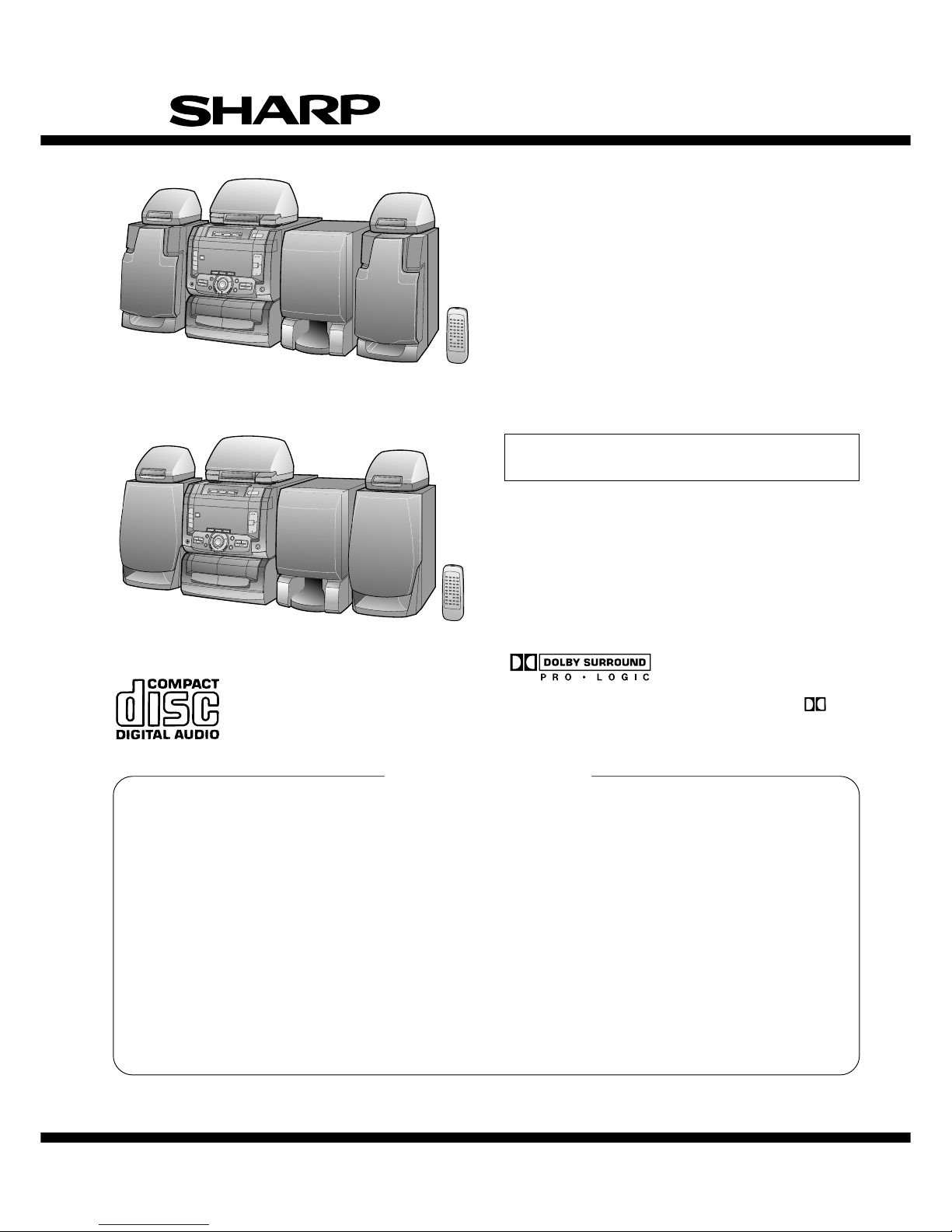
Illustration: CD-C472
Illustration: CD-C3400/C3400C/C3800/C3800C
CONTENTS
Page
IMPORTANT SERVICE NOTES (For U.S.A. Only) .......................................................................................................... 2
SPECIFICATIONS .............................................................................................................................................................3
NAMES OF PARTS .......................................................................................................................................................... 4
OPERATION MANUAL..................................................................................................................................................... 6
QUICK GUIDE .................................................................................................................................................................. 7
DISASSEMBLY................................................................................................................................................................. 8
REMOVING AND REINSTALLING THE MAIN PARTS.................................................................................................. 11
ADJUSTMENT................................................................................................................................................................ 12
NOTES ON SCHEMATIC DIAGRAM ............................................................................................................................. 15
WAVEFORMS OF CD CIRCUIT..................................................................................................................................... 16
BLOCK DIAGRAM .......................................................................................................................................................... 17
SCHEMATIC DIAGRAM / WIRING SIDE OF P.W.BOARD.............................................................................................20
TROUBLESHOOTING (CD CHANGER CONTROL / CD SECTION) ............................................................................ 34
FUNCTION TABLE OF IC .............................................................................................................................................. 38
FL DISPLAY.....................................................................................................................................................................44
REPLACEMENT PARTS LIST/EXPLODED VIEW
PACKING OF THE SET (For U.S.A. Only)
CD-C472
CP-C472, CP-SW472, CENTER(GBOXS0006AWM1)
and REAR(GBOXS0007AWM1), Constitute CD-C472.
CD-C3400/C3400C
CP-C3400, CP-SW472, CENTER(GBOXS0006AWM1)
and REAR(GBOXS0007AWM1), Constitute CD-C3400/C3400C.
CD-C3800/C3800C
CP-C3800, CP-SW3800, CENTER(GBOXS0006AWM3)
and REAR(GBOXS0007AWM3), Constitute CD-C3800/C3800C.
• In the interests of user-safety the set should be restored to its
original condition and only parts identical to those specified be
used.
Manufactured under license from Dolby Laboratories Licensing Corporation. DOLBY, the double-D symbol and
"PRO LOGIC" are trademarks of Dolby Laboratories Licensing Corporation.
SERVICE MANUAL
This document has been published to be used
for after sales service only.
The contents are subject to change without notice.
SHARP CORPORATION
CD-C472/C3400/C3400C/C3800/C3800C
– 2 –
FOR A COMPLETE DESCRIPTION OF THE OPERATION OF THIS UNIT, PLEASE REFER
TO THE OPERATION MANUAL.
IMPORTANT SERVICE NOTES (For U.S.A.Only)
BEFORE RETURNING THE AUDIO PRODUCT
(Fire & Shock Hazard)
Before returning the audio product to the user, perform the
following safety checks.
1. Inspect all lead dress to make certain that leads are not
pinched or that hardware is not lodged between the chassis
and other metal parts in the audio product.
2. Inspect all protective devices such as insulating materials,
cabinet, terminal board, adjustment and compartment
covers or shields, mechanical insulators etc.
3. To be sure that no shock hazard exists, check for leakage
current in the following manner.
* Plug the AC line cord directly into a 120 volt AC outlet.
* Using two clip leads, connect a 1.5k ohm, 10 watt resistor
paralleled by a 0.15µF capacitor in series with all exposed
metal cabinet parts and a known earth ground, such as
conduit or electrical ground connected to earth ground.
* Use a VTVM or VOM with 1000 ohm per volt, or higher,
sensitivity to measure the AC voltage drop across the
resistor (See diagram).
* Connect the resistor connection to all exposed metal parts
having a return path to the chassis (antenna, metal cabinet,
screw heads, knobs and control shafts, escutcheon, etc.)
and measure the AC voltage drop across the resistor.
All check must be repeated with the AC line cord plug connection
reversed.
Any reading of 0.3 volt RMS (this corresponds to 0.2 milliamp.
AC.) or more is excessive and indicates a potential shock
hazard which must be corrected before returning the audio
product to the owner.
TO EXPOSED
METAL PARTS
CONNECT TO
KNOWN EARTH
GROUND
TEST PROBE
0.15 µ F
1.5k ohms
10W
VTVM
AC SCALE

– 3 –
CD-C472/C3400/C3400C/C3800/C3800C
Front speaker section
Type: 2-way 4-3/4" (120 mm) woofer and 2" (50
mm) tweeter type
Maximum input power: 50 W
Impedance: 8 ohms
Dimensions: Width; 7-1/8" (180 mm)
Height; 11-13/16" (300 mm)
Depth; 8-1/2" (216 mm)
Weight: 5.7 lbs. (2.6 kg)/each
Type: 3-way type 4-3/4" (120 mm) woofer, 2"
(50 mm) tweeter and super tweeter]
Maximum input power: 50 W
Impedance: 8 ohms
Dimensions: Width; 7-7/8" (180 mm)
Height; 11-13/16" (300 mm)
Depth; 8-1/2" (215.5 mm)
Weight: 5.5 lbs. (2.5 kg)/each
Center speaker section
Type: 4" (100 mm) full range speaker
Maximum input power: 20 W
Impedance: 6 ohms
Dimensions: Width; 10-5/16" (262 mm)
Height; 5-3/4" (145 mm)
Depth; 7-15/16" (201 mm)
Weight: 2.6 lbs. (1.2 kg)
Rear speaker section
Type: 4" (100 mm) full range speaker
Maximum input power: 10 W
Impedance: 12 ohms
Dimensions: Width; 6-3/4" (170 mm)
Height; 4-13/16" (122 mm)
Depth; 6-15/16" (176 mm)
Weight: 1.3 lbs. (0.6 kg)/eac
Sub woofer section
Type: 5-1/8" (130mm) full range speaker
Maximum input power: 60 W
Impedance: 6 ohms
Dimensions: Width; 7-7/8" (200 mm)
Height; 11-13/16" (300 mm)
Depth; 11-11/16" (297 mm)
Weight: 7.9 lbs. (3.6 kg)
CP-C472
CP-C3400/C3800
GBOXS0006AWM1/3
GBOXS0006AWM1/3
General
Power source: AC 120 V, 60 Hz
Power consumption: 100 W
Dimensions: Width; 10-5/8" (270 mm)
Height; 11-13/16" (303 mm)
Depth; 13-13/16" (350 mm)
Weight: 14.0 lbs. (6.4 kg)
Amplifier section
Output power: Front speakers; 25 W minimum RMS into
8 ohms from 60 Hz to 20 kHz with no
more than 10 % total harmonic distortion.
Center speaker; 10 W
(1 kHz, 10 % T.H.D.)
Rear speakers; 10 W (total)
(1 kHz, 10 % T.H.D.)
Sub woofer; 30W
(80Hz, 10% T.H.D.)
Output terminals: Front speakers; 8 ohms
Center speakers; 6 ohms
Rear Speakers; 12 ohms
Sub woofer; 6 ohms
Headphones; 16-50 ohms
(recommended; 32 ohms)
Input terminal: Video/Auxiliaary (audio signal);
500 mV/47 kohms
Tuner section
Frequency range: FM; 87.5 - 108 MHz
AM; 530 - 1,720 kHz
Cassette deck section
Frequency response: 50 - 14,000 Hz (Normal tape)
Signal/noise ratio: 55 dB (TAPE 1, playback)
50 dB (TAPE 2, recording/playback)
Wow and flutter: 0.15 % (WRMS)
Compact disc player section
Type: 3-disc multi-play compact disc player
Signal readout: Non-contact, 3-beam semiconductor
laser pickup
D/A Converter: 1-bit D/A converter
Frequency response: 20 - 20,000 Hz
Dynamic range: 90 dB (1 kHz)
Specifications for this model are subject to change without prior notice.
SPECIFICATIONS
CD-C472/C3400/
C3400C/C3800/C3800C
CP-SW472/SW3800
CD-C472/C3400/C3400C/C3800/C3800C
– 4 –
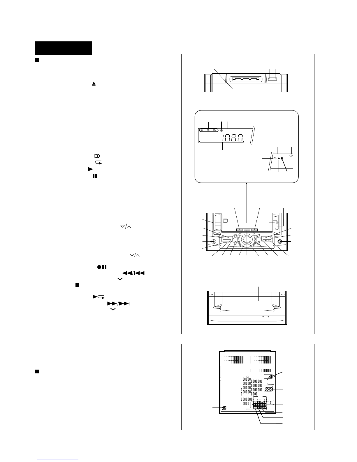
NAMES OF PARTS
Rear Panel
1. AC Power Input Socket
2. FM/AM Loop Aerial Socket
3. Video/Auxiliary (Audio Signal) Input Sockets
4. Sub woofer Terminals
5. Rear Speaker Terminals
6. Center Speaker Terminals
7. Front Speaker Terminals
Front Panel
1. Disc Tray
2. Disc Number Selector Buttons
3. Disc Skip Button
4. Open/Close Button:
5. Disc Number Indicator
6. Timer Indicator
7. Record Indicator
8. Sleep Indicator
9. Extra Bass Indicator: X-BASS
10. Function/CD Track/CD Counter/Frequency/Preset
Channel/Volume/Timer/Sleep Time Indicator
11. Memory Indicator
12. FM Stereo Mode Indicator: ST
13. FM Stereo Indicator:
14. CD Repeat Indicator:
15. CD Play Indicator:
16. CD Pause Indicator:
17. Power Button
18. Bypass Button
19. Phantom Button
20. Extra Bass Button: X-BASS
21. Main Volume Up/Down Buttons:
22. Function Selector Buttons
23. Timer/Sleep Button
24. Clock Button
25. Headphone Socket
26. Tuning and Time Up/Down Buttons:
27. Memory/Set Button
28. Record Pause Button:
29. (CD)Track Down/Review Button:
(TUNER)Preset Down Button:
30. Stop Button:
31. Normal Button
32. Play/Repeat Button:
33. (CD)Track Up/Cue Button:
(TUNER)Preset Up Button:
34. Equalizer Selector/Demo Mode Button
35. CD Pause Button
36. Random Button
37. Clear Button
38. Sub woofer volume Control
39. (TAPE 1) Cassette Compartment
40. (TAPE 2) Cassette Compartment
CD-C472/C3400/
C3400C/C3800/C3800C
1234
17 18 19 20
21
22
23
24
25
26
30
31 32 33
34
35
27
2829
37
36
38
39
40
MEMORY ST
kHz
MHz
1 2 3
REC
SLEEP
X-BASS
56789
10
11
12
13
14
15 16
1
2
3
4
5
6
7
– 5 –
CD-C472/C3400/C3400C/C3800/C3800C
CP-C472
Speaker Section
Front Speaker
1. Tweeter
2. Woofer
3. Bass Reflex Duct
4. Speaker Wire
5. Tweeter
6. Super Tweeter
7. Woofer
8. Bass Reflex Ducts
9. Speaker Wire
Center Speaker
10. Full Range Speaker
11. Speaker Wire
Sub woofer
12. Full Range Speaker
13. Speaker Wire
Rear Speaker
14. Full Range Speaker
15. Speaker Wire
1
2
3
4
5
6
8
7
9
10
11
12
13
14 15
16
17
18 19
20 21
24
25
26
27
22
23
28
CP-C3400/C3800
CP-SW472/SW3800
GBOXS0006AWM1/3
CD-C472/C3400/
C3400C/C3800/C3800C
Remote Control
1. Remote Control Transmitter LED
2. Surround Level Buttons:
3. Center Level Buttons:
4. Dolby Pro Logic Button
5. Center Mode Button
6. Test Tone Button
7. Balance Control Buttons:
Tuner control section
8. Preset Up/Down Buttons:
CD Control section
9. Disc Skip Button
10. Play/Repeat Button:
11. Memory Button
12. Clear Button
13. Pause Button:
14. Track Down/Review Button:
15. Track Up/Cue Button:
16. Stop Button:
17. Random Button
GBOXS0006AWM1/3
15
14
10
11
12
13
2
3
1
4
5
6
7
8
9
CP-C472
Front Speaker
CP-C3400/3800
Front Speaker
Tape control section
18. (TAPE 1) Play Button:
19. (TAPE 1/2) Stop Button:
20. (TAPE 2) Play Button:
21. (TAPE 2) Record Pause Button:
22. (TAPE 2) Rewind Button:
23. (TAPE 2) Fast Forward Button:
24. Equalizer Mode Button
25. Function Selector Buttons
26. Power Button
27. Extra Bass Button: X-BASS
28. Volume Up/Down Buttons:
CD-C472/C3400/C3400C/C3800/C3800C
– 6 –
OPERATION MANUAL
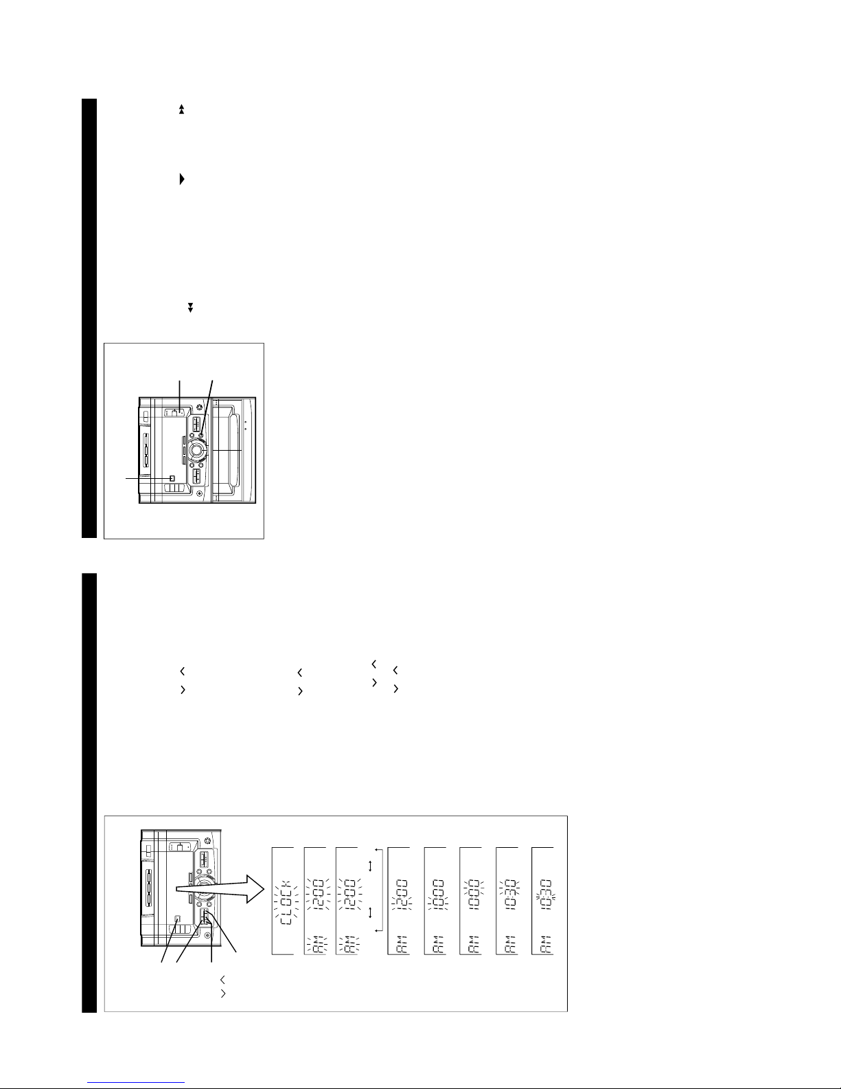
SETTING THE CLOCK
POWER
CLOCK
MEMORY/
SET
TUNING/
TIME
( )
AM 12:00 AM 0:00 0:00
2
3
4
7
6
5
8
9
(Main unit operation)
1 Press the POWER switch to turn the power off.
2
Press the CLOCK button.
3 Within 3 seconds, press the MEMORY/SET button.
4 Press the TUNING/TIME ( or ) button to select the time
display mode.
"AM 12:00" → The 12-hour di splay will ap pear.
(AM 12:00 - PM 11:59)
"AM 0:00" → The 12-hour display will appear.
(AM 0:00 - PM 11:59)
"0:00" → The 24-h our display will a ppear.
(0:00 - 23:59)
● Note that this can only be set when the unit is first installed
or it has been reset (see page 18).
5 Press the MEMORY/SET button.
6 Press the TUNING/TIME ( or ) button to adjust the hour.
● Press the TUNING/TIME button once to advance the time by
1 hour. Hold it down to advance continuously.
● When the 12-hour display is selected, "AM" will change auto-
matically to "PM".
7 Press the MEMORY/SET button.
8 Press the TUNING/TIME ( or ) button to adjust the
minutes.
● Press the TUNING/TIME ( or ) button once to advance
the time by 1 minute. Hold it down to change the time in 5
minute intervals.
● The hour setting will not advance even if minutes advance
from "59" to "00".
9 Press the MEMORY/SET button.
● The clock starts operating from "0" seconds. (Seconds are
not displayed.)
Note:
● In the event of a power failure or when the AC power cord
is disconnected, the clock display will go out.
When the AC power supply is restored, the clock display will
flash on and off to indicate the time when the power failure
occurred or when the AC power cord was disconnected.
If this happens, follow the procedure below to change the
clock time.
To change the clock time:
When the POWER switch is set to OFF.
① Press the MEMORY/SET button.
② Perform steps 6 - 9 above.
When the POWER switch is set to ON.
① Press the CLOCK button.
② Within 3 seconds, press the MEMORY/SET button.
③ Perform steps 6 - 9 above.
To see the time display:
Press the CLOCK button.
● The time display will appear for about 3 seconds.
To change the time display mode:
① Perform steps 1 - 2 in the section "RESETTING THE MICRO-
COMPUTER", on page 18.
② Perform steps 1 - 9 above.
In this example, the clock is set for the
12-hour (AM 12:00) system.
RESETTING THE MICROCOMPUTER
Reset the microcomputer under the following conditions:
● To erase all of the stored memory contents (clock and timer
settings, and tuner and CD presets).
● If the display is not correct.
● If the operation is not correct.
1
Press the POWER switch to turn the power off.
2
While pressing down the VOLUME button and the /
button, hold down the POWER button for at least 1 sec-
ond.
Caution:
● The operation explained above will erase all data stored in
memory including clock and timer settings, and tuner and CD
presets.
1,2
2
2
– 7 –
CD-C472/C3400/C3400C/C3800/C3800C
MINI COMPONENT SYSTEM
CD-C472
Quick-Guide
Guía rápida
Preparation fo r use
Preparación pa ra su uso
8 OHMS
MIN.
6 OHMS
MIN.
6 OHMS
MIN.
12 OHMS
MIN.
RIGHT
RATED SPEAKER IMPEDANCE:
LEFT
RIGHT
LEFT
SPEAKERS
FRONT
CENTER
REAR
SUB WOOFER
A
B
C
D
A
B
C
D
+
+
15
15
POWER
POWER
Turning the power on
and off
Conexión y desconexión de la alimentación
Remote control
Control remoto
CD playback
Reproducción d e discos compactos
Precaution
OPEN
/CLOSE
OPEN
/CLOSE
C D
● AM Loop Antenna
●
Antena de cuadro de AM
● FM Antenna
●
Antena de
FM
● AC 120 V, 60 Hz
●
120 V de CA, 60 Hz
White line
Línea blanca
White line
Línea blanca
White line
Línea blanca
Red
Rojo
Black
Negro
Red
Rojo
Red
Rojo
Black
Negro
Black
Negro
● 2 "AA" batteries
●
Dos pilas "AA"
● Batteries are not included.
●
Las pilas no están incluidas.
Remote Sensor
Sensor remote
8" - 20' (0.2m - 6m)
0,2m - 6m
● Label facing up
●
Etiqueta hacia arriba
● The sound level at a given volume setting
depends on a combination of speaker efficiency,
location and many other factors. It is advisable
to avoid exposure to high volume levels, which
occur while turning the unit on with the volume
control setting up high, or while continually
listening at high volume levels.
● Only discs bearing the logo as
shown can be played in this
unit.
TAPE 1
TAPE
(1 2)
TAPE 2
REC PAUSE
C D
TAPE 2
TUNER
(BAND)
TUNING/TIME
ST
FM STERO
FM MONO
AM
VOLUME
UP • • •
X-BASS
DOWN •
VOLUME
FLAT HEAVY-1
HEAVY-2
SOFT-2
SOFT-1
VOCAL
Recording from CDs
Grabación de dis cos compactos
Tape playback
Reproducc ión de cintas
Radio operation
Funcionamiento de la radio
Precaución
Sound control
Control del sonido
Load the disc to be
recorded.
Introduzca el disco
que va a grabar.
VOLUME
UP • • •
X-BASS
DOWN •
X-BASS
CD recording
starts.
La grabación de
CD empieza.
•
El nivel de sonido en una posición de volumen
fijado depende de una combinación del
rendimiento de las altavoces, la posición y
muchos otros factores. Es aconsejable evitar
un aumento de volumen. Esto se produce, por
ejemplo, al conectar el aparato con el volumen
puesto en una posición alta. Evite continuar la
audición prolongada a altos
niveles de sonido.
•
En este aparato sólo pueden
reproducirse los discos que
tengan el logotipo mostrado.
Main volume
Sub woofer volume
Equalizer
Extra-BASS
Volumen principal Volumen de subgraves
Ecualizador
Graves extra
SUB WOOFER
VOLUME
MIN MAX
DEMO
EQUALIZER
EQUALIZER
MODE
CD-C472/C3400/C3400C/C3800/C3800C
– 8 –
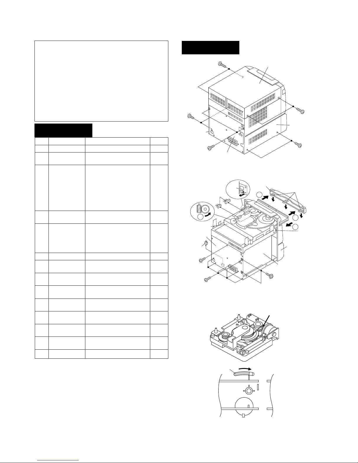
DISASSEMBLY
Caution on Disassembly
Follow the below-mentioned notes when disassembling
the unit and reassembling it, to keep it safe and ensure
excellent performance:
1. Take cassette tape and compact disc out of the unit.
2. Be sure to remove the power supply plug from the wall
outlet before starting to disassemble the unit.
3. Take off nylon bands or wire holders where they need be
removed when disassembling the unit. After servicing
the unit, be sure to rearrange the leads where they were
before disassembling.
4. Take suffcient care on static electricity of integrated
circuits and other circuits when servicing.
Figure 8-2
Figure 8-3
CD-C472/C3400/
C3400C/C3800/C3800C
1 Top Cabinet 1. Screw ..................... (A1) x4 8-1
2 Side Panel 1. Screw ..................... (B1) x6 8-1
(Left/right) 2. Screw ..................... (B2) x2
3 CD Player Unit/ 1. Turn on the power supply, 8-2
CD Tray Cover open the disc tray, take out
the CD cover, and close.
(Note 1)
2. Hook....................... (C1) x3
3. Hook....................... (C2) x2
4. Screw ..................... (C3) x1
5. Socket .................... (C4) x2
4 Back Board 1. Screw ..................... (D1) x9 8-2
2. Socke ..................... (D2) x1
5 Main PWB 1. Screw ..................... (E1) x1 9-1
2. Socket .................... (E2) x2
3. Flat Wire................. (E3) x1
4.Tip Wire................... (E4) x1
5.Socket ..................... (E5) x1
6 Front Panel 1. Screw ..................... (F1) x2 9-1
7 Display PWB/ 1. Socket .................... (G1) x1 9-2
Switch PWB 2. Screw .....................
(G2) x13
8 Tape Mechanism 1. Open the cassette holder. 9-2
2. Screw...................... (H1) x5
9
Power Amp. PWB
1. Screw ..................... (J1) x3 9-3
2. Socket .................... (J2) x2
10 Turntable 1. Screw ..................... (K1) x1 9-4
2. Cover ..................... (K2) x1
11 Disc Tray 1. Screw ..................... (L1) x2 9-4
2. Guide ..................... (L2) x2
12 CD Player Unit 1. Screw..................... (M1) x1 9-5
2. Socket .................... (M2) x4
13 CD Changer 1. Screw ..................... (N1) x4 9-6
Mechanism 1. Screw
14 CD Mechanism 1. Screw ..................... (P1) x1 9-6
STEP REMOVAL PROCEDURE FIGURE
Note 1:
How to open the changer manually. (Fig. 8-3)
1. Insert the tip of fine screwdriver into the hole of CD player
base, and press down the worm wheel < A > .
2. Then, turn fully the lock lever in the arrow direction through
the hole on the loading chassis bottom in this state.
After that, push forward the CD player base.
CD-C472/C3400/
C3400C/C3800/C3800C
Figure 8-1
( B1 ) x2
ø3 x8mm
( B2 ) x2
ø3 x8mm
( B1 ) x2
ø3 x8mm
Top Cabinet
Side Panel
(Right)
Rear Panel
Side Panel
(Left)
( A1 ) x2
ø3 x12mm
( A1 ) x2
ø3 x12mm
CD Tray Cover
CD Player Unit
( D1 ) x2
ø3 x10mm
( D1 ) x7
ø3 x8mm
( C3 ) x1
ø3 x8mm
Hook
( C1) x3
( C2 ) x1
( D2 ) x1
( C4 ) x2
Back Board
Main PWB
Front Panel
1
1
2
A
Pull
(C2) x1
LOCK
LEVER
< A >
– 9 –
CD-C472/C3400/C3400C/C3800/C3800C
Figure 9-1
Figure 9-2
Figure 9-3
Care when installing the CD changer mechanism.
Install the CD changer mechanism on the CD player base after
the shift lever has been set in the highest position.
Figure 9-4
Figure 9-5
Figure 9-6
Display
PWB
Switch PWB
Open
Front Panel
( G2 ) x3
ø3 x10mm
( G2 ) x10
ø3 x10mm
( H1 ) x5
ø3 x10mm
( G1 ) x1
Tape
Mechanism
Cassette
Holder
(Left/Right)
( E2 ) x2
( E3 ) x1
(E5) x1
( E4 ) x1
( E1 ) x1
ø3 x10mm
( F1 ) x2
ø3 x8mm
Main PWB
Push
Push
Front Panel
Tape
Mechanism
Power Amp.
PWB
( J1 ) x3
ø3 x12mm
( J2 ) x1
( J2 ) x1
Power Amp.
PWB
Power
Transfomer
( L1 ) x1
ø3 x10mm
( L1 ) x1
ø3 x10mm
( K1 ) x1
ø3 x10mm
Turntable
Disc Tray
( K2 ) x1
( L2 ) x1
( L2 ) x1
CD Player Unit
( M1 ) x1
ø3 x10mm
( M2 ) x2
( M2 ) x2
CD Player Unit
( N1 ) x4
ø3 x12mm
( P1 ) x1
ø2.6 x10mm
CD Changer
Mechanism
CD Mechanism
Shift Lever
CD Player Base
CD-C472/C3400/C3400C/C3800/C3800C
– 10 –
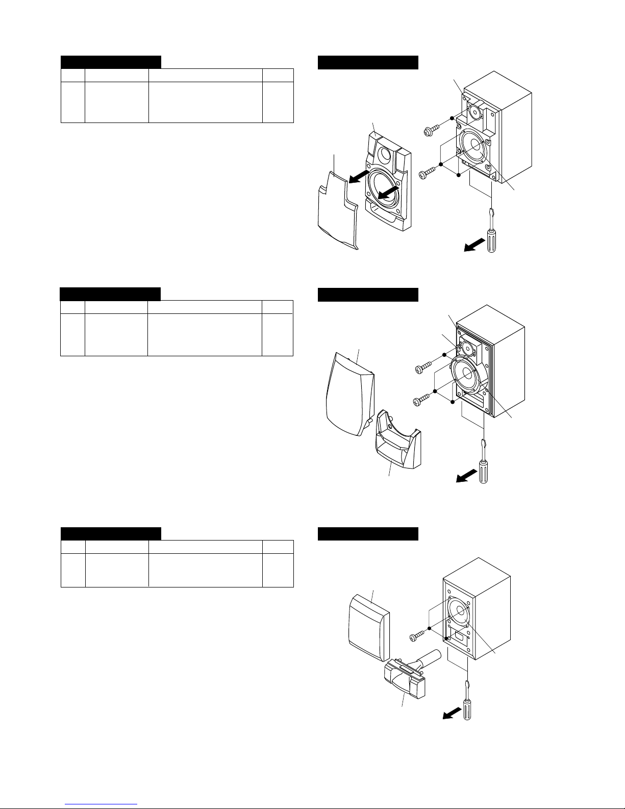
CP-C472
1 Front Speaker 1. Net.......................... (A1) x1 10-1
2. Front Panel ............ (A2) x1
3. Screw ..................... (A3) x2
4. Screw ..................... (A4) x4
STEP REMOVAL PROCEDURE FIGURE
CP-C472
( A3 ) x2
ø3 x10mm
( A4 ) x4
ø3 x12mm
Screwdriver
Net
( A1 ) x1
Front Panel
( A2 ) x1
Woofer
Tweeter
Figure 10-1
Screwdriver
Woofer
Tweeter
Super
Tweeter
( A4 ) x4
ø4 x12mm
( A3 ) x2
ø3 x10 mm
( A1 ) x1
( A2 ) x1
Figure 10-2
CP-C3400/C3800
CP-SW472/SW3800
( A3 ) x4
ø3 x12mm
Net
( A1 ) x1
( A2 ) x1
Screwdriver
Woofer
Figure 10-3
CP-C3400/C3800
1 Front Speaker 1. Net.......................... (A1) x1 10-2
2. Duct Panel ............. (A2) x1
3. Screw ..................... (A3) x2
4. Screw ..................... (A4) x4
STEP REMOVAL PROCEDURE FIGURE
CP-SW472/SW3800
1 Sub woofer 1. Net.......................... (A1) x1 10-3
2. Duct Panel ............. (A2) x1
3. Screw ..................... (A3) x4
STEP
REMOVAL PROCEDURE FIGURE
Note:
The center and rear speakers can be easily disassembled.
Therefore the disassembling method is not discribed.
For details refer to the disassembling drawing in the Parts
Guide.
– 11 –
CD-C472/C3400/C3400C/C3800/C3800C
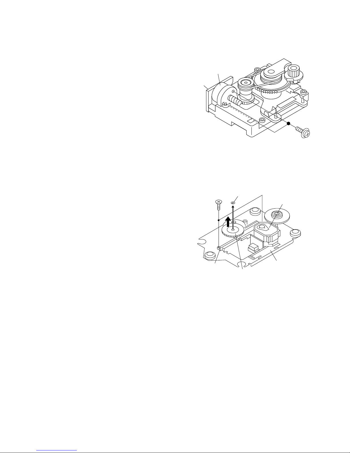
How to remove the pickup (See Fig. 11-2)
1. Remove the screws (B1) x 2 pcs., to remove the shaft (B2).
2. Remove the stop washer (B3) x 1 pc., to remove the gear
(B4).
3. Remove the pickup.
Figure 11-2
REMOVING AND REINSTALLING THE MAIN PARTS
CD MECHANISM SECTION
Perform steps 1, 2, 3, 13 and 14 of the disassembly method
to remove the CD mechanism.
How to remove the loading motor
(See Fig. 11-1)
1. Remove the screws (A1) x 2 pcs., to remove the loading
motor.
Figure 11-1
( A1 ) x2
ø2.6 x5mm
Loading / Up
/ Down Motor
Motor
PWB
( B1 ) x2
ø2.6 x6mm
Shaft
( B2 ) x1
Stop Washer
( B3 ) x1
Gear
( B4 ) x1
CD Mechanism
Pickup
CD-C472/C3400/C3400C/C3800/C3800C
– 12 –
MECHANISM SECTION
• Driving Force Check
Torque Meter Specified Value
Play: TW-2412 Tape 1: Over 80 g
Tape 2: Over 80 g
• Torque Check
Torque Meter
Tape 2
Play: TW-2111 30 to 60 g. cm 30 to 60 g.cm
Fast forward: TW-2231 — 60 to 120 g.cm
Rewind: TW-2231 — 60 to 120 g.cm
Specified
Value
Adjusting
Point
Instrument
Connection
Test Tape
Normal MTT-111 Volume in 3,000 ± Speaker
speed motor. 30 Hz terminal
(MM1) (Load
resistance:
8 ohms)
ADJUSTMENT
Specified Value
Tape 1
• Tape Speed
• AM IF/RF
Signal generator: 400 Hz, 30%, AM modulated
*1. Input: Antenna, Output: TP302
*2. Input: Antenna, Output: TP301
TUNER SECTION
fL: Low-range frequency
fH: High-renge frequency
IF 450 kHz 1,720 kHz T351 *1
Band — 530 kHz (fL): T302 *2
Coverage 1.1 ± 0.1 V
Tracking 990 kHz 990 kHz (fL): T302 *1
Test Stage Frequency Frequency
Display
Setting/
Adjusting
Parts
Instrument
Connection
*1. Input: Antenna, Output: TP301
*2. Input: Antenna, Output: Speaker terminal
• FM RF
Signal generator: 1 kHz, 75 kHz dev., FM modulated
Band — 87.50 MHz L303(fL): *1
Coverage 3.4 V ± 50 mV
RF 98.00 MHz 98.00 MHz L302 *2
(10-30 dB)
Test Stage
Instrument
Connection
Frequency
Frequency
Display
Serring/
Adjusting
Point
• Detection
Signal generator: 10.7 MHz, FM sweep generator
Detection 10.7 MHz 98.00 MHz T352 Input: Pin 1 of
IC303
Output: TP302
IF 10.7 MHz 98.00 MHz T301(Turn Input: Pin 1 of
the core of IC301
transformer Output: TP302
T352 fully
counterclookwise.)
Instrument
Connection
Test
Stage
Adjusting
Parts
Frequency
Display
Frequency
Adjusting
Parts
Instrument
Connection
Frequency
Display
Frequency
• VCO Frequency
* Adjust for 76 kHz ± 200 Hz.
Notes:
After preparing the test circuit shown in Fig 12-2, connect the
Pin 13 , Pin 21 and ground of the IC303 with test circuit, and
measure the Value.
At this time, apply a standard unmodulated signal input and
adjust the VCO.
Pin 13 of IC303
Pin 21 of IC303
D
G
S
10 kΩ
TO FREQUENCY
COUNTER
FET : 2SK19 or 2SK54
Figure 12-2
TAPE MECHANISM
MM 1
Motor
Volume in motor
98.00 MHz 98.00 MHz VR351* Pin 13, Pin 21
(60 dB) and ground
of IC303
Figure 12-1 ADJUSTMENT POINTS
IC301
IC303
MAIN PWB
13
1
1
21
FM BAND
COVERAGE fL
T301
R316
L303
TP301
L302
T351
T352
TP302
R340
T302
VR351
VCO
AM IF
FM RF
FM DET
FM IF
AM TRACKING
fL
AM BAND
COVERAGE fL
– 13 –
CD-C472/C3400/C3400C/C3800/C3800C
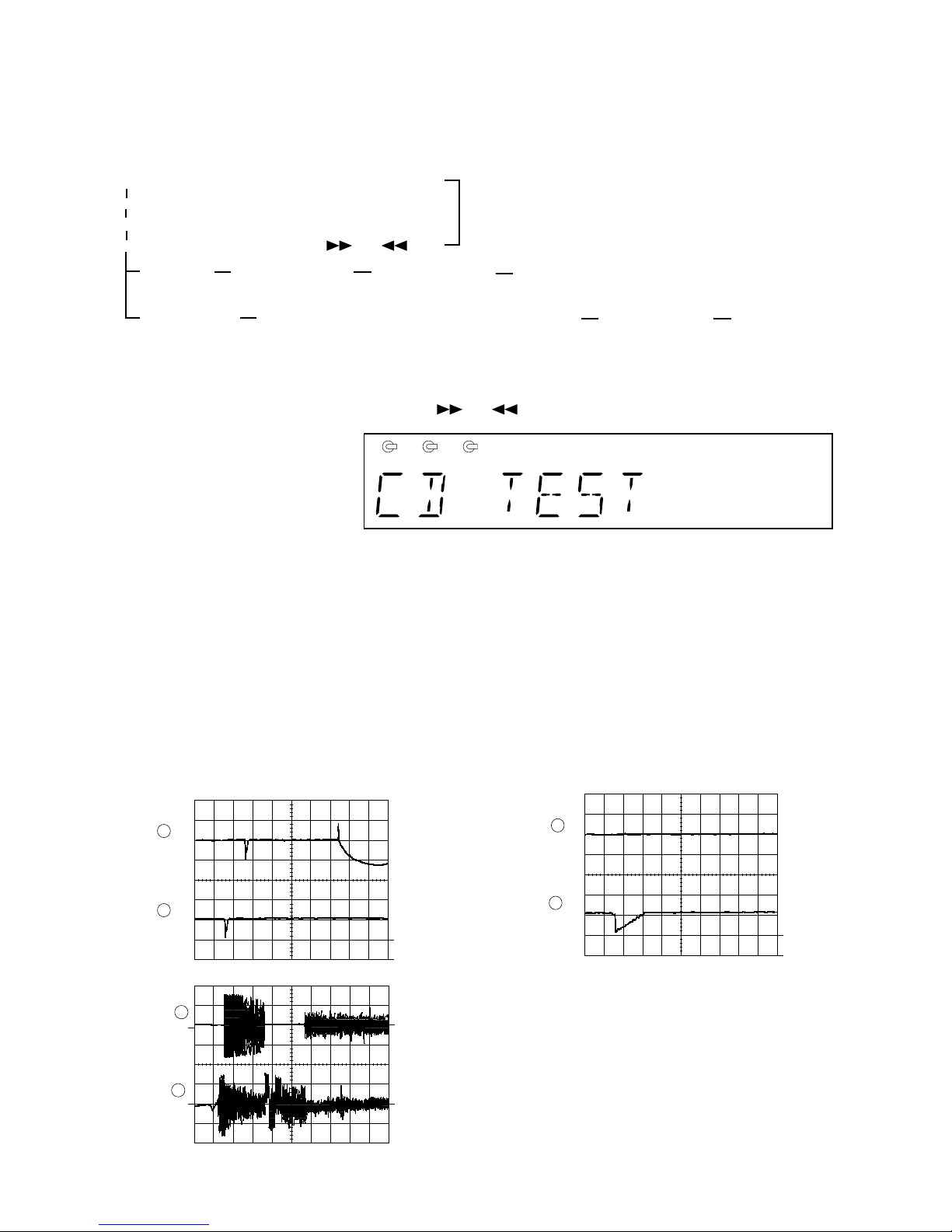
TEST MODE
2
1
TO
TE
200 ms
1V/diV
IC 1 15
200 ms
1V/diV
IC 1 7
TRACKING/
ERROR
BARANCE
ADJUST
Figure 13-2
Figure 13-3
2
1
10ms
0.50 V
IC1 20 FE
10ms
0.50 V
IC1 7 TE
Enlarged
View
TRACKING
OFF-SET
ADJUST
Since this CD system incorporates the following automatic adjustment function, when the pickup is replaced, it is not necessary
to readjust it.
Since this CD unit does not need adjustment, the combination of PWB and laser pickup unit is not restricted.
• Automatic adjustment item
1. Focus offset (Fig. 13-2)
2. Tracking offset (Fig. 13-3)
3. E/F balance (tracking error balance) (Fig. 13-4)
4. RF level AGC function (HF level: constant)
5. RF level automatic follow-up of the tracking gain
This automatic adjustment is performed each time a disc is changed. Therefore,
each disc is played back using the optimal settings.
CD SECTION
Figure 13-1
Note:
Only in STOP state it is possible to slide the pickup with the ( ) or ( ) key.
VOL. --- Last memory
BAL. --- CENTER
R.GEQ. --- FLAT
X-BAS --- OFF
Canceling method - POWER OFF
• Setting the test mode
Any one of test mode can be set by pressing several keys as follows.
<REC. PAUSE> + <DISC. SKIP> + <POWER> TEST: CD operation test
• TEST mode
Function — CD test mode
Setting of TEST mode
Indication of CD TST mode (Fig. 13-1)
OPEN/CLOSE operation is manual operation.
The pickup can be moved by using the (
) or ( ) key.
<MEMORY>
LASER ON
<PLAY> key input
Press <STOP> key.
Stop
TOC. IL is performed, and the ordinary PLAY is performed.
If the following key is pressed during PLAY, it is possible
to specify directly any Track No.
<Disc Number 1> key: Track 4
<Disc Number 2> key: Track 9
<Disc Number 3> key: Track 15
<MEMORY>
Tracking on the spot.
SERVO OFF PLAY
<MEMORY>
Tracking on the spot.
SERVO ON PLAY
STOP
2
0.1s
0.50 V
IC1 20 FE
0.1s
0.50 V
IC1 7 TE
1
FOCUS
OFF-SET
ADJUST
TRACKING
OFF-SET
ADJUST
Figure 13-4
IL is not performed.
<STOP>
1 2 3
CD-C472/C3400/C3400C/C3800/C3800C
– 14 –
SP out L-ch Input signal is output.
(SO901) R-ch Input signal is output.
(SO901) SP out C-ch SP cut, no output
(SO901) SP out S-ch
Almost no output (only omitting component)
SP out L-ch Almost no output (only omitting component)
(SO901) R-ch Almost no output (only omitting component)
(SO901) SP out C-ch
Input signal is output.
(SO901) SP out S-ch
Almost no output (only omitting component)
State of set Dolby Pro Logic Dolby Pro Logic On mode
Output point Bypass mode Normal mode Phantom mode
IC501 12 pin L-out Output enabled state Output enabled state Output enabled state
11 pin R-out Output enabled state Output enabled state Output enabled state
IC501 9pin C-out No output Output enabled state No output
IC501 10pin S-out No output Output enabled state Output enabled state
SP OUT L-ch Output enabled state Output enabled state Output enabled state
(SO901) R-ch Output enabled state Output enabled state Output enabled state
SP OUT C-ch No output in MUTE (Q604) state Output enabled state No output in MUTE (Q604) state
(SO901)
SP OUT S-ch No output in MUTE (Q603) state Output enabled state Output enabled state
(SO901)
EXPLANATION OF DOLBY SURROUND PRO LOGIC AND EVALUATION METHOD
Test tone output
• Pro Logic ON Normal mode
Press the remote control TEST TONE button.
→Output of only L-ch →Output of only C-ch
↑ ↓
Output of only S-ch ← Output of only R-ch
The test tone (noise) is repeatedly output for output period
(2 sec).
In this case the following indication appears repeatedly.
→TEST →L-ch →C-ch
↑ ↓
S-ch ← R-ch
• Pro Logic ON Phantom mode
Press the remote control TEST TONE button.
→Output of only L-ch →Output of only R-ch
↑ ↓
← Output of only S-ch
The test tone (noise) is repeatedly output for output period
(2 sec).
In this case the following indication appears repeatedly.
→TEST → L-ch → R-ch
↑ ↓
← S-ch←
Outline
• Namely, two speakers are connected in parallel to one
amplifier.
• In the Pro Logic BYPASS mode the amplifier for C-ch (center
channel) and the amplifier for S-ch (surround channel) are in
MUTE state. The SP output is cut.
• In the normal mode of Pro Logic ON mode the amplifiers for
C-ch and S-ch are in operative state, so that the SP output
appears.
• In the Phantom mode of Pro Logic ON mode the amplifier for
C-ch is in MUTE state, so that the SP output is cut. The
amplifier for S-ch (surround) is in operative state, so that the
SP output appears
• State of element output and terminal output in specific mode
Relation between VIDEO IN input and output in Pro Logic
ON state
(1) L-ch/R-ch same phase input into VIDEO IN input jack in
VIDEO Function mode
Output point Normal mode
Output point Phantom mode
(2) L-ch/R-ch reverse phase input into VIDEO IN input jack in
VIDEO Function mode
(Reverse phase: Phase difference between L and R is 180°)
Output point Normal mode
SP out L-ch
Almost no output (only omitting component)
(SO901) R-ch
Almost no output (only omitting component)
(SO901) SP out C-ch
Almost no output (only omitting component)
(SO901) SP out S-ch Input signal is output.
Output point Phantom mode
SP out L-ch
Almost no output (only omitting component)
(SO901) R-ch
Almost no output (only omitting component)
(SO901) SP out C-ch SP cut, no output
(SO901) SP out S-ch Input signal is output.
• Accordingly, if you want to output signal waveform to C-ch SP
out, give the same phase input into L-ch/R-ch INPUT in the
Pro Logic Normal mode.
If one of channels receives input, C-ch does not output. Only
L-ch or R-ch outputs.
• If you want to output signal waveform to S-ch SP out, you can
use either Normal mode or Phantom mode. However, 180°
reverse phase input must be given to L-ch/R-ch INPUT.
– 15 –
CD-C472/C3400/C3400C/C3800/C3800C
• The indicated voltage in each section is the one measured
by Digital Multimeter between such a section and the chassis with no signal given.
1. In the tuner section,
( ) indicates AM
< > indicates FM stereo
2. In the main section, a tape is being played back.
3. In the deck section, a tape is being played back.
( ) indicates the record state.
4. In the power section, a tape is being played back.
5. In the CD section, the CD is stopped.
• Parts marked with “ ” ( ) are important for
maintaining the safety of the set. Be sure to replace these
parts with specified ones for maintaining the safety and
performance of the set.
NOTES ON SCHEMATIC DIAGRAM
• Resistor:
To differentiate the units of resistors, such symbol as K and
M are used: the symbol K means 1000 ohm and the symbol
M means 1000 kohm and the resistor without any symbol is
ohm-type resistor. Besides, the one with “Fusible” is a fuse
type.
• Capacitor:
To indicate the unit of capacitor, a symbol P is used: this
symbol P means micro-micro-farad and the unit of the
capacitor without such a symbol is microfarad. As to
electrolytic capacitor, the expression “capacitance/withstand
voltage” is used.
(CH), (TH), (RH), (UJ): Temperature compensation
(ML): Mylar type
(P.P.): Polypropylene type
• Schematic diagram and Wiring Side of P.W.Board for this
model are subject to change for improvement without prior
notice.
REF. NO
DESCRIPTION
POSITION POSITION
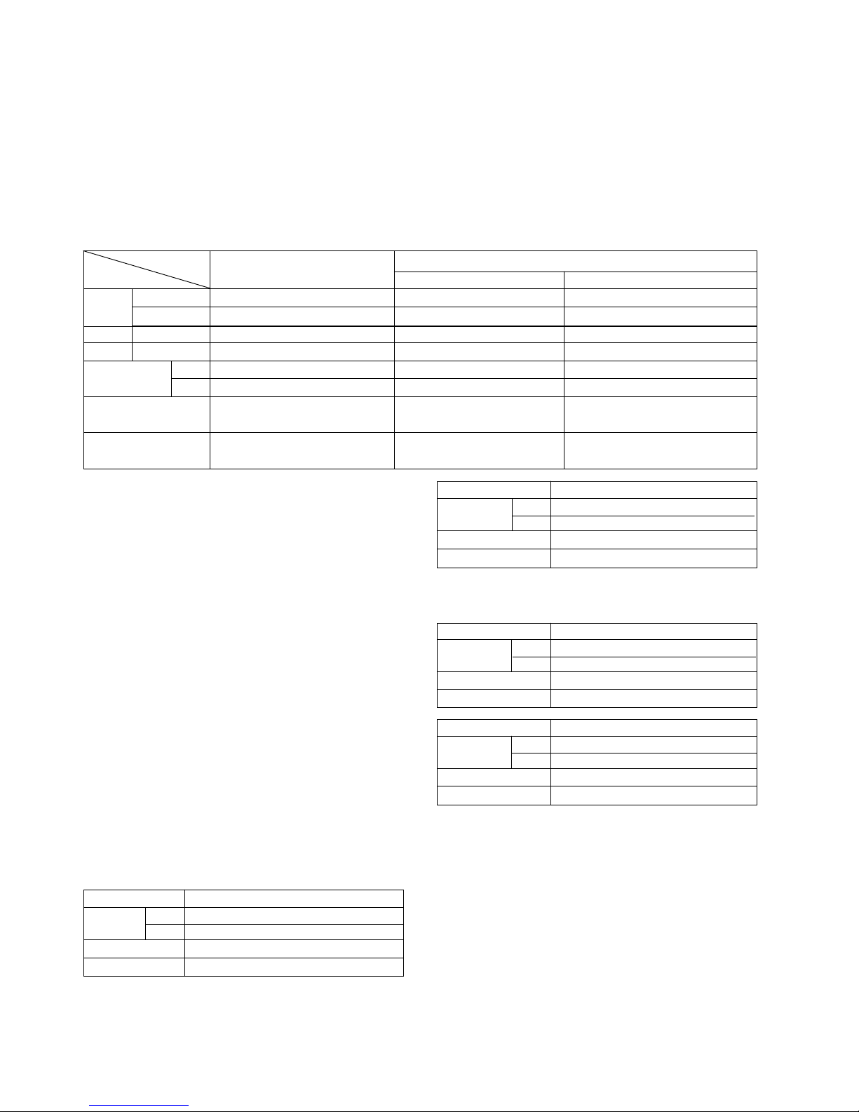
SW716 TUNING DOWN ON—OFF
SW717 POWER ON—OFF
SW718 CLOCK ON—OFF
SW719 TIMER/SLEEP ON—OFF
SW720 MEMORY/SET ON—OFF
SW721 CD ON—OFF
SW722 TUNER/BAND ON—OFF
SW723 TAPE ON—OFF
SW724 VIDEO/AUX ON—OFF
SW725 PASS ON—OFF
SW726 NORMAL ON—OFF
SW727 PHANTOM ON—OFF
SW728 CD PAUSE ON—OFF
SW729 CD CLEAR ON—OFF
SW730 RANDOM ON—OFF
SWM 3 FOOL PROOF ON—OFF
SWM 4 F.A.S. ON—OFF
SWM 5 CAM ON—OFF
REF. NO
DESCRIPTION
SW1 OPEN/CLOSE ON—OFF
SW2 MECHA UP ON—OFF
SW3 DISC NUMBER ON—OFF
SW4 PICKUP IN ON—OFF
SW701 EQUALIZER/DEMO ON—OFF
SW702 VOLUME DOWN ON—OFF
SW703 X-BASS ON—OFF
SW704 VOLUME UP ON—OFF
SW705 OPEN/CLOSE ON—OFF
SW706 DISC SKIP ON—OFF
SW707 DISC 1 ON—OFF
SW708 DISC 2 ON—OFF
SW709 DISC 3 ON—OFF
SW710 REC. PAUSE ON—OFF
SW711 UP ON— OFF
SW712 STOP ON—OFF
SW713 PLAY ON—OFF
SW714 DOWN ON—OFF
SW715 TUNING UP ON—OFF
2SA1015 GR
2SC535 C
2SD468 C
KRA102 M
KRA109 M
KRC102 M
KRC104 M
KRC107 M
KTA1266 GR
KTA1271 Y
KTC3199 GR
KTC3200 GR
KTC3203 Y
ECB
(S)(G)(D)
(1) (2) (3)
FRONT
VIEW
BCE
(D)(G)(S)
(3) (2) (1)
FRONT
VIEW
2SD2012
Figure 15 TYPES OF TRANSISTOR
CD-C472/C3400/C3400C/C3800/C3800C
– 16 –
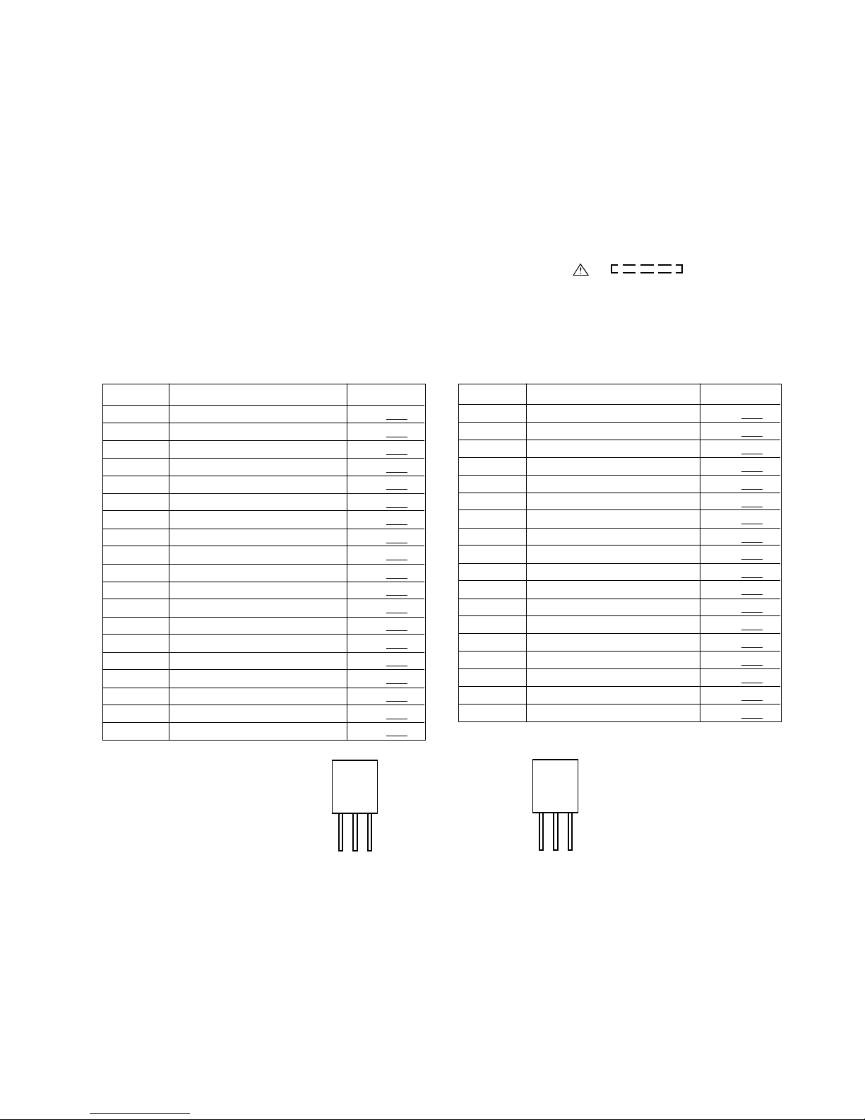
WAVEFORMS OF CD CIRCUIT
3
5ms
0.50 V
IC1 20 F.E
1
5ms
5.0 V
IC1 54 DRF
STOP PLAY
FOCUS SERCH
1
3
5
4
2
6
7
8
9
10
11
3
4
5
6
7
8
9
6
7
8
10
11
12
9
6
7
8
9
12
0.5ms
1.00 V
HF
0.5ms
5.0 V
HFL
0.5ms
5.0 V
TES
1
2
3
CUE
0.5ms
1.00 V
HF
1
2
3
0.5ms
5.0 V
HFL
0.5ms
5.0 V
TES
REVIEW
50ms
10.0 V
JP+
CUE
50ms
10.0 V
JP-
50ms
0.50 V
JP
50ms
1.00 V
TE
0.5ms
10.0 V
JP+
0.5ms
10.0 V
JP-
0.5ms
0.50 V
JP
0.5ms
1.00 V
TE
REVIEW
50ms
10.0 V
JP+
50ms
10.0 V
JP-
50ms
0.50 V
JP
50ms
1.00 V
TE
0.5ms
10.0 V
JP+
0.5ms
10.0 V
JP-
0.5ms
0.50 V
JP
0.5ms
1.00 V
TE
PLAY
20ms
1.00 V
SPO
NORMAL DISC
TN0=01
20ms
2.00 V
CLV+
PLAY
TCD-712 (140mm)
TN0=01
50ms
1.00 V
SPO
50ms
2.00 V
CLV+
PLAY
TCD-712
5s
100mV
SLD
1
0.5s
100mV
SLD
1

– 17 –
CD-C472/C3400/C3400C/C3800/C3800C
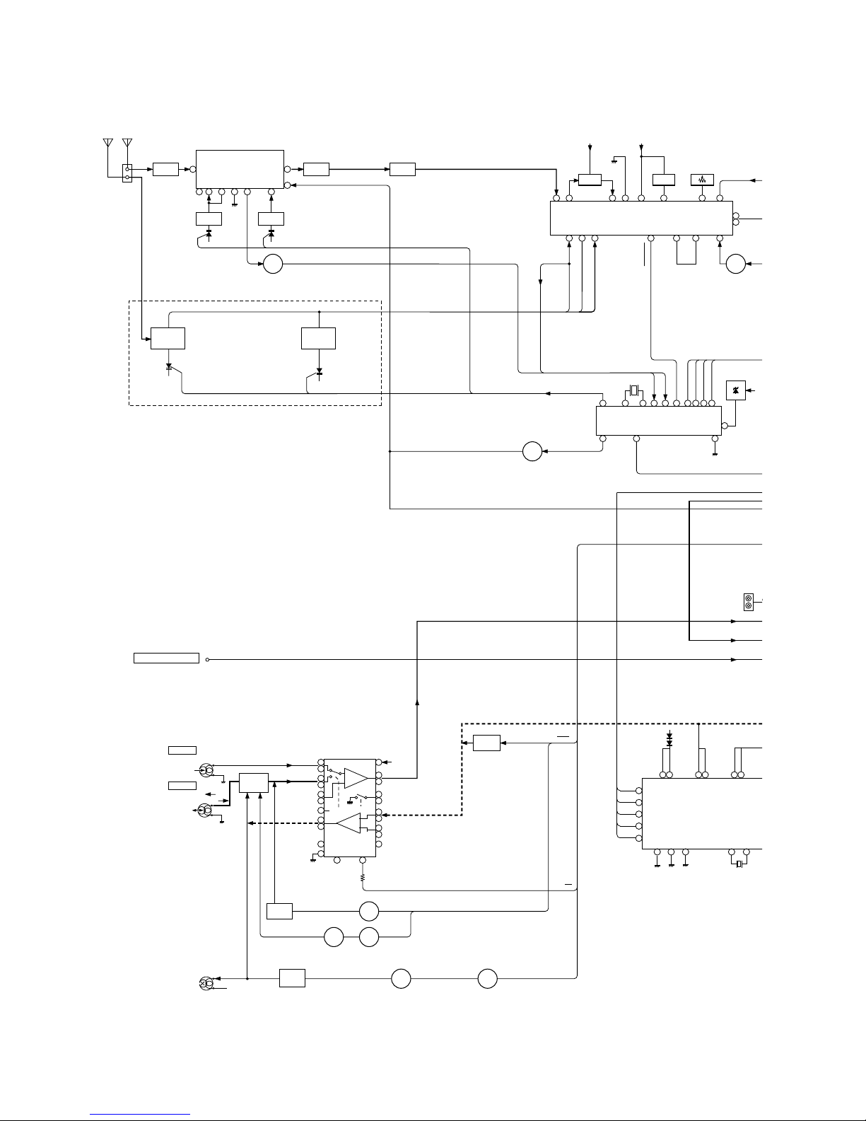
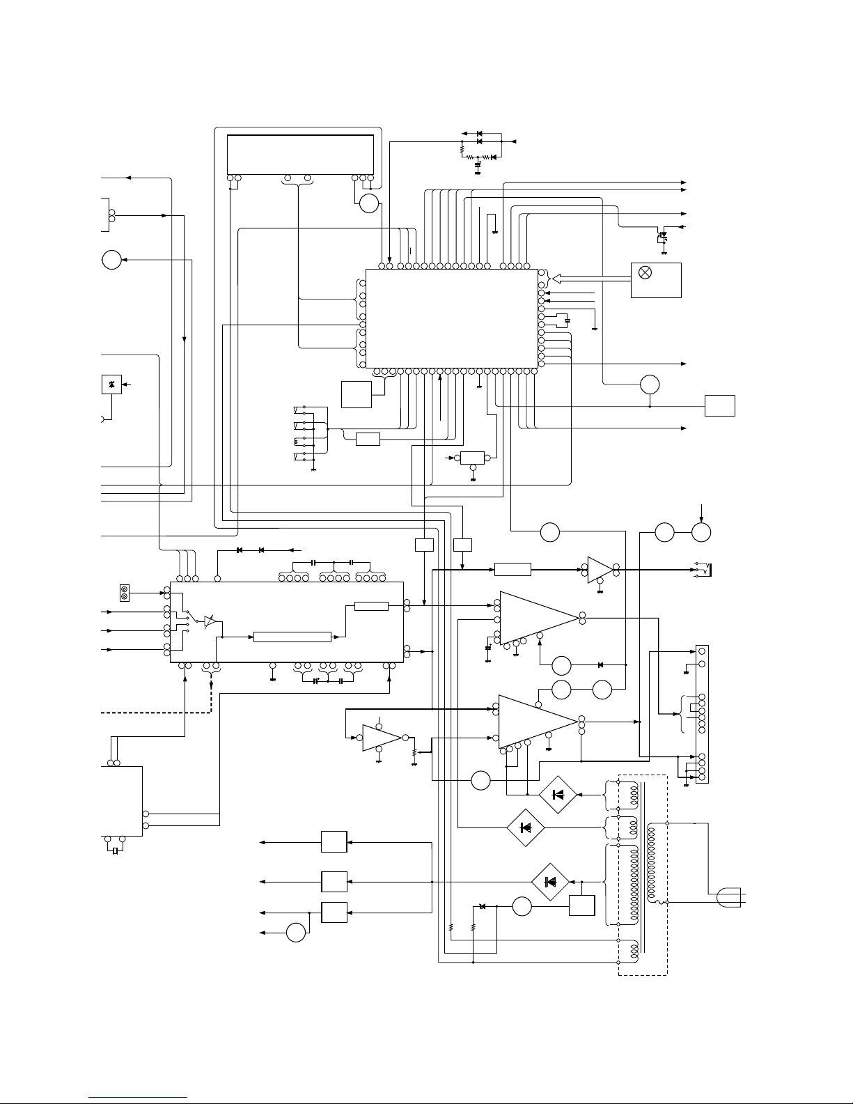
Figure 17 BLOCK DIAGRAM (1/3)
1
2
3
4
5
98
6
7
20
12
13
242530
31
3222
34
35
36
10 11
27
26
28
29
PU-IN SW
XL1
XIN
LD0
FIN2
JP–
CV+
SLC
SL1
FIN1EF
TO
FD
SPO
NC
SLD
SL–
SL+
DRF
CL
DAT
CE
VCC1
6
+5V
PICKUP IN
SW4
FOCUS COIL
TRACKING COIL
M1
DISC
MOTOR
M
M
M2
SLIDE
MOTOR
PICKUP UNIT
9
IC2
LC78623D
SERVO/SIGNAL
CONTROL
+B1
IC3
M56748FP
DRIVER
IC1
LA9241M
SERVO AMP.
6
1
9
5
+B1
+12V(+B5)
( TO IC601 )
RES. CQCK. COIN
SQOUT. RWC. WRQ
~
~
~
CL, DAT, SELIAL CONTROL/CE
Q93
Q91
SL+. SL–. DRF
7
3
9
8
7
6
5
4
3
2
1
GND (D)
MECHA UP
GND (D)
DISK NO.
OPEN/CLOSE
GND (D)
M–M+GND (M)
9
8
7
6
5
4
3
2
1
CNP10
M
+5V
+B1
62
64 45 3623 43
37
38
39
40
24
25
10 10
265853
101220
324043
44
5352515431302923271615
4144
Q1
Q52
+4.3V
Q81 +7.3V (B1)
REGULATOR
TO MAIN SECTION
IC81
TA7291S
LORDING MOTOR
DRIVER
XOUT
EFMO
EFMIN
CLV+
JP–
CONT2
CONT1
RCHO
RVSS
LVSS
LCHO
VVDD
VDD
LVDD
RVDD
XVDD
SW1
OPEN/CLOSE
SW2
MECHA UP
SW3
DISC No.
M3
LOADING
SOLM1
TO DISPLAY
SECTION
CNS10
CD-C472/C3400/C3400C/C3800/C3800C
– 18 –
Figure 18 BLOCK DIAGRAM (2/3)
J501
VIDEO/AU
X
L
R
L-CH
R-CH
PB HEAD
1
2
3
4
L NF
L (T1)
R (T1)
L (T2)
R (T2)
R NF
4
5
13
21
24
23
18
17
10
1915
12
14
16
20
H/N
6
7
8
9
T1/T2
POP REDUCE
L REC
R REC
R NF
REC
L NF
P.B.
REC
L-CH
R-CH
REC/PB
HEAD
ERASE
HEAD
BIAS
OCS
REF
ALC
HIGH
NOR/
T1/T2
1
GND
3
4
5
1
X352
4.5MHz
OSC
7
STEREO
FM/AM
SWITCHING
ST
ST
1
234
57
8
6
FM IF
OSC BUFF
AM IF
FM IF IN
VT
FM RF FM OSC
FM
OSC
FM IN
AMIN
FM
5
3
AM MIX
AM IF
6
9
FM/AM
FM+B
21
20 13 15
10
111617
DET OUT
MPX IN
24
2223
AM OSC IN
AM+B
AM RF IN
FM DET
VCO
FM DET
MO/ST
+B4
9
AM TRACKING
AM BAND
COVERAGE
+B4
L
R
PLAYBACK&RECORD/
PLAYBACK AMP.
IC101
AN7345K
L
R
P.B
IC301
FM FRONT END
TA7358AP
FM BPF
FM/AM IF
IC303
LA1805
TA
P
A
TU
C
D
FROM CD SECTION
Q128
L104
Q124
Q126
BIAS
Q103
Q106
~
P.B
REC
AC BIAS
Q107
Q108
Q111
Q109 Q110
T1/T2
MUTING
Q121
Q122
REC
+B4
L
R
Q344
7
6
CE
DI
CL
DO
22
10
20
15 16
21
17
11
Q343
T351
T352
VR351
CF301
T301
L303
Q302
L302
T302
AM ANT.
IC302
LC72131
PLL CONTROLLER
FM
MPX VCO ADJ
TAPE 1
TAPE 2
R
L
FM OSC
BF301
SWITCHING
SWITCHING
SWITCHING
SWITCHING
SWITCHING
FM&AM LOOP ANT
VOLTAGE
REGURATER
+
B
SWITCHING
BIAS
FM +B
RT-IN
LT-IN
L-OUT
R-OUT
CL
+B4
CL
DATA
DATA
ENABLE
X501
8
18
45
44
23
24
IC501
LV1035M
DOLBY PRO LOGIC
DECORDER
38
35
37
36
42
33
31 32
34
21
– 19 –
CD-C472/C3400/C3400C/C3800/C3800C
Figure 19 BLOCK DIAGRAM (3/3)
13
4
4
3
11
STAND-BY
L
J501
VIDEO/AUX
R
L
R
R
REAR-OUT
CENTER
OUT
FM/AM
WITCHING
ST FM
9
M
10
MONO/ST
T
FM
9
2
5
12
14
REAR-IN
CENTER-IN
7
VCC
14
NF
8
+12V (ANALOG)
+B4
+12V (MOTOR)
+5.6V
+B5
+B1
L
R
OUT
IC951
LA4451
POWER AMP.
+B4
PRESET GRAPHIC EQUALIZER
VDD
X-BASS
VSS
GRAPHIC EQUALIZER
VOLUME
20
28
REAR
CENTER
R
R
L
L
L
TAPE
AUX
TUNER
CD
7
Q343
VOLTAGE
REGULATOR
VOLTAGE
REGULATOR
VOLTAGE
REGULATOR
+B1
+
–
SUB WOOFER
+
–
+
–
+
–
REAR SPEAKER
CENTER SPEAKER
JA901
HEADPHONES
M901
FAN MOTOR
+7.3V
Q820
Q822
Q824
Q825
Q823
Q826
IC601
LC75396E
AUDIO PROCESSOR
23
52
60
53
59
54
58
55
57
49 6348 64 26
4425436
44
24 25 56
CLDICE
OLTAGE
GURATER
+B4
25
27
29
30
33
34
35
36
37
38
39
40
42 41434445464748495051 4352535455565859
60
65
70
57
2423222120191817
80
72
71
16151413121110
9
~
6
1
~
~
~
7
8
3
RX701
Q707~
Q709
LED701~
LED706
2
1
SYSTEM STOP
DO
DRF
DI
DE
CL
RESET
XL701
4.19MHz
AVDD
AVREF
VDD
+B2
KEY
SW701
SW730
TO POWER SECTION
+B5
PHM1
RESET
Q705
Q706
ZD701
MEMORY
BACK UP
+B2
3
2
1~
3330 31 32
Q701
+B2
+B1
UNSWITCH
FL701
DISPLAY
~
61
64
~
POWER
C-MUTE
T.F
AC 120V 60Hz
AC POWER
SUPPLY CORD
VOLTAGE
REGULATOR
Q801
Q903
Q901 Q902
Q710
D807
D809
~
D803 ~ D806
ZD801
Q704
IC701
IX0192AW
SYSTEM CONTROL
MICROCOMPUTER
TO CD SECTION
TO CD SECTION
TO CD SECTION
TO CD SECTION
16
19
3
4
8
4
3
5
L-OUT
FRONT
R-OUT
SUB-WOOFER OUT
SUB-WOOFER
IN
12
18
1
R-IN
FRONT
L-IN
VR701
SUB WOOFER
VOLUME
–B
+B
+B4
IC901
STK40724
POWER AMP.
IC451
NJM4558L
SUB WOOFER AMP.
D801
D802
12
39
9
36
11
40
8
37
10
41
7
38
+
–
+
–
FRONT SPEAKER
SO901
SPEAKER TERMINAL
CD PUIN
CD SL+
CD SL–
VDD
TAPE SOL
TAPE MOTOR
TAPE MECHASTOP
TAPE FP
R MUTE
D.P.CE
T1 RUN PLSE
SOLM1
SOLENOID
SWM5
CAM
SWM4
F. A. S
SWM3
FOOL PROOF
L-CH INPUT
R-CH INPUT
T2 RRUN PLSE
CD UP DOWN/DISC NO
CD DSP RES
CD T/T OPEN/CLOSE
RESET
CD DSP SQOUT
CD DSP COIN
CD DSP RWC
CD DSP CQCK
CD DSP WRQ
T1/T2
TAPE REC
TAPE BIAS
Q603
Q604
Q601
Q602
F-MUTE
F-MUTE
3018
LRIN
RRIN
RTIN
LTIN
17
31
R
L
L-OUT
R-OUT
X501
23
24
OGIC
R
22
9
31 32
S- OUT
C-OUT
7
3
5
1
7
IC681
NJM4560L
HEADPHONE AMP.
Q905Q605
M
Q671 Q672
Q673 Q674
H/P MUTE
+B1
+
–
9
8
20
Q705
Q706
Q904
CD-C472/C3400/C3400C/C3800/C3800C
– 20 –
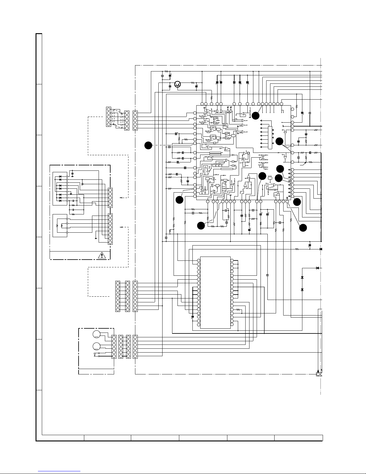
Figure 20 SCHEMATIC DIAGRAM (1/10)
A
B
C
D
E
F
G
H
1
23456
• NOTES ON SCHEMATIC DIAGRAM can be found on page 15.
1
2
3
4
5
5
4
3
2
1
8
7
1
5
4
3
2
1
6
5
4
3
2
8
7
2
3
4
5
6
8
7
2
3
4
5
6
M
M
11
6
5
4
3
2
1
6
5
4
3
2
1
6
5
4
3
2
1
6
5
4
3
2
1
8
7
6
5
4
3
2
1
5
4
3
2
1
2200P
1M
2200P
1M
PD
VR
LD
TR–
TR+
FO+
FO–
GND
PD
VR
LD
TR–
TR+
FO+
FO–
GND
PICKUP UNIT
ACTUATOR
TR–
FO–
FO+
TR+
LD GND
LT0H30M1
C
F
A
B
E
K
LD
MON
CD MOTOR PWB-E
–
+
–
+
CNP12
C33
0.47/50
C34
0.33/50
R21
22K
R22
22K
D1
1SS1
3
R37
82K
R26
82K
C13
330P
IC1
LA9241M
SERVO AMP.
R45
4.7K
R38
470
R46
560
C2
0.01
C1
100/16
R2
1K
C12
0.1
R14
27K
R131KC9
0.047
D2
RL104A
D4
RL104A
C84
0.001
R12
100
C7
0.1/50
C8
0.068
C10
180P
R15
12K
R16
3.3K
C18
0.47/50
R31
1.2K
C26
0.033
R40
5.6K
C24
2.2P
C27
0.001
C30
0.1/50
C31
220/6.3
C32
0.01
R32
10K
R33
1.2K
C19
1/50
C20
47/16
R36
220K
C21
0.0033
R35
220K
D3
RL104A
C11
0.1
R18
15K
R1
22
C35
1/50
C4
0.1/50
C14
0.01
C28
0.1
C29
4.7/50
R17
33K
R24
47K
R23
10K
R25
1.5K
R27
39K
C16
0.0047
R9
100K
R8
15K
C54
0.001
C5
0.033
R10
2.2K
C6
0.033
R11
6.8K
IC3
M56748FP
FOCUS/TRACKING/SPIN/SLIDE DRIVER
C36
100/16
R48
10K
R34
22K
C3
1/50
R19
1K
R20
1K
R30
6.8K
C17
0.001
R29 56K
R28 10K
R42
47K
R44
33K
R43
56K
R41
47K
C15
0.01
R3
9
1K
C25
27P
Q1
KTA1266 GR
12
36
35
34
33
32
31
30
29
28
27
26
25
24
23
22
21
20
19
17
18
16
9
6
15
14
13
12
11
10
8
7
5
4
3
2
1
1
2
3
4
5
6
7
8
9
10
11
12
13
14
15
16
17 18 19 20 21 22 23 24 25 26 27 28 29 30 31 32
33
34
35
36
37
38
39
40
41
42
43
44
45
46
47
48
49505152535455565758596061626364
CD_PUIN
SL_–
SL_+
SP–
SP+
WRQ(DSP)
RWC(DSP)
CD_GND
TP1
HF
FE1
SLOF
SLOF
FSC
FOSTA
TE
F
E
B
A
K
K
E
B
A
F
K
E
B
A
F
4.2V
1.5V
4.8V
CV+
CV–
SLOF
HFL
TES
TOFF
TGL
JP+
JP–
RFSM
RFS–
SLC
RF
REF
OR
REF
REF
REF
REF
SL+
SL–
SLD
SLEO
SPO
SP–
SPG
SPI
SP
AGND
FE–
FEFAFA–
FD–
GEN
GEN
GEN
FD
TO
JP
TD–
TD
TH
REF
JP
REF
TO
REF
REF
REF
REF
REF
REF
REF
REF
REF
REF
REF
SCI
TESI
TE
TE–
TB
F
E
FIN1
FIN2
VCC1
LDS
BHI
PHI
LF2
VR
REF1
VCC2
DRF
CE
DAT
CL
CLK
DEF
SLI
DGND
REF
LDO
RF
REF
REF
FE1
VCR
VCR
VCR
VCR
TGL1
THDL
GL
THD
VCC
DEF
HFL
DRF
CE
CL
SLOF
FSTA
LATOH
TOSTA
FOSTA
S.Q.R
FSTA
8/12CM
LASER
2FREQ
JP+
JP–
CV+
CV–
REF
REF
JP
REF
-
+
EFBAL
FSC
SLOF
JPCLO
FSS
TBC
CNS1B
CNS1A
CNS2B
CNS2A
CNP3A
CNS3B
CNS3A
M1
DISC
MOTOR
M2
SLIDE
MOTOR
SW4
PICKUP
IN
CNP3
CNP2
CNP1
+B +B
+B
+
–
+
–
+
–
+
–
+
–
+
–
+
–
+
–
+
–
+
–
+
–
+
–
+
–
+
–
+
–
+
–
+
–
+
–
+
–
+
–
+
–
+
–
+
–
+
–
+
–
+
–
+
–
+
–
+
–
+
–
2.5V
2.5V
2.5V
2.5V
2.5V
2.5V
2.4V
2.5V
2.5V
2.5V
2.5V
2.4V
2.5V
2.5V
2.4V
2.4V
0V
2.2V
2.2V
2.5V
2.5V
2.5V
2.5V
2.5V
2.5V
2.5V
0V
2.5V
2.4V
2.5V
2.5V
2.5V
0V
0V
4.8V
0V
0V
4.8V
4.8V
0V
1.5V
2.4V
2.5V
2.4V
0V
2.5V
0V
2.5V
4.8V
0V
2.2V
1V
1V
2.5V
2.5V
4.8V0V0V4V4V
2.4V
0V
4.2V
4.8V
4.7V
0V
0V
0V
2V
2.5V
2.5V
2V
2V
0V
0V
0V
2V
2.5V
2.5V
0V
2.5V
2.5V
4.7V
0.7V
2.5V
0V
1.8V
2.5V
2.5V
2V
2V
0V
0V
0V
1.8V
2.5V
2.5V
0V
0V
0V
10
5
4
3
2
9
6
7
1
8

– 21 –
CD-C472/C3400/C3400C/C3800/C3800C
Figure 21 SCHEMATIC DIAGRAM (2/10)
7
8 9 10 11 12
• The numbers 1 to 12 are waveform numbers shown in page 16.
12
CNP11
D1
1SS133
C44
100P
C45
100P
C47
100P
C22
220P
C23
0.0027
38
0
R53
1.2K
C74
220P
C73
220P
R73
390
R74
390
C43
330/6.3
C48
100P
C49
100P
C81
47/16
C57
0.001
D4
RL104A
R62 1K
R63 1K
C38
0.01
R61 1K
R57 1K
6
33
R60
1K
R52
27K
C40
0.047
C39
0.047
R50
680
R90 1K
R89 1K
R83
3.9
C83
0.022
D82
1SS133
D81
1SS133
C72
10/50
C71
10/50
R93
220
C35
1/50
R88 1K
C28
0.1
CNP10
R51
3.3M
R42
47K
R44
33K
3
1
R39
1K
5
P
IC2
LC78623D
SERVO/SIGNAL
CONTROL
C46
100P
C53
0.022
R47
10K
C37
0.022
Q91
KTA1271 Y
Q93
KRC102 M
R87
10K
R86
2.2K
D91
1SS133
R82
3.3K
C82
47/16
L61
0.82µH
C51
100/16
ZD61
MTZJ5.6B
R66
220
R64
22
C52
100/16
Q52
KTC3203 Y
C56
0.022
R72
2.7K
R71
2.7K
C50
0.022
R55
150
R81
2.7K
R85
56
(1/2W)
C75
0.001
11 12 13
6789
10
14
12345
1221
1
2
3
4
5
6
10
9
8
7
6
5
4
3
2
1
10
9
8
7
6
5
4
3
2
1
6
1
2
3
4
5
46
47
49
5660
61
1
13
24
38
37
36
35
34
33
323130292827262523222120191817
16
15
14
12
11
10
9
8
7
6
5
4
3
2
64
63
62
59
58
57
555453
52
51
50
39
40
41
42
43
44
45
48
123456789
R59 1K
R58 1K
12V
6.5V
0V0V0V
6.4V1V6.5V
6.5V
2.9V
BIM5
FSEQ
EMPH
CONT5
C2F
TEST3
LVSS
MUTEL
MUTER
SBSY
EFLG
UP/DOWN
DISC NO.
OPEN/CLOSE
PUIN SW
SLD–
SLD+
D_GND
DRF (ASP)
RES(DSP)
CQ CK(DSP)
SQ OUT(DSP)
CO IN(DSP)
WRQ(DSP)
RWC(DSP)
UP/DOWN
GND(D)
DISC NO.
OPEN/CLOSE
GND(D)
M+
GND(M)
SOL
GND(D)
CNS10
SW3
DISC NUMBER
CNS5
SW2
MECHA UP
SW1
OPEN
CLOSE
SENSOR
PWB-F
CD SERVO PWB-C
M3 T/T
UP/DOWN
LOADING
LOCK
SOLM2
SOLENOID
0V
12V
CD_LD_M–
CD_LD_M+
R-CH
TO MAIN PWB
P22 2-A
CNS11
A_GND
L-CH
D-GND
7.3V
M_12V
6.5V
5.5V
CD_LCH
4.9V
+5V
A_GND
CD_RCH
XL1
X-TAL
GENERATOR
4M
16M
/RES
/CQCK
COIN
SQOUT
RWC
WRQ
FSX
PW
SFSY
SBCK
TEST11
U-COM
INTERFACE
SUB-CODE
XVSS
XIN
XOUT
XVDD
RVDD
RCHO
RVSS
LCHO
LVDD
NC
TEST4
TEST1
1BIT
DAC
4FS
DIGITAL
FILTER
DOUT
DIGITAL
OUT
ERROR COERECT
FLAG CONTROL
VCO CLOCK
OSC CONTROL
SLICE LEVEL
CONTROL
SYNC-DETECT
EFM DEMODULATE
EXTERNAL
OUTPUT
CLV
DIGITAL SERVO
CONT4
CONT3
CONT2
CONT1
VDD
PCK
JP–
JP+
TGL
TOFF
DEF1
PDO
VVSS
ISET
VVDD
FR
VSS
EFMO
EFMIN
TEST2
CLV+
CLV–
V/P
HLF
TES
SERVO
COMMAND
2KX8
RAM
M
TA1
/CS
TEST5
0V
0V
12V
3
2
1
IC81
TA7291S
LOADING MOTOR DRIVER
TO DISPLAY PWB
P25 11-A
CNS12
+B
+B
+B
+B
+B
+B
+B
+B
+B
–
+
M–
0V
0V
0V
1.9V
4.8V
0V
0V
2.5V
2.5V
0V
0V
0V
4.8V
0V
0V
0V
0V
0V
0V
4.8V0V2.5V
0V
0V0V0V
4.8V
2.5V
0V
0V
4.8V
4.8V
2.4V
2.5V
4V4V4V0V0V
0V
2.4V0V2.4V
0V
0V
0V0V0V
0V
4.8V
4.8V
0V
2.2V
0V
2.1V
2.2V
4.8V
4.5V
2V
0V
2V
4.5V
0V
0V
CD SIGNAL
10

CD-C472/C3400/C3400C/C3800/C3800C
– 22 –
A
B
C
D
E
F
G
H
1
23456
• NOTES ON SCHEMATIC DIAGRAM can be found on page 15.
Figure 22 SCHEMATIC DIAGRAM (3/10)
R529
330
R636
10K
D602
1SS133
D603
1SS133
C524 10/50
R510
18K
C521 0.33/50
R503
1K
C506 0.022
C50 47/25
C516 0.15/50
C542
220/16
C510 0.47/50
C512 4.7/50
C515 0.0033 (ML)
C503 1/50
C533 0.47/50
R509
4.7K
C551 100P
C520 0.15/50
C522 0.15/50
C527 10/50
C531
2.2/50
R511
1K
C550 100P
C537 10/50
C540
10/50
C535 10/50
C538 10/50
D516
RL104A
C539 220/16
R512
4.7K
R502
100K
C546
220P
C549 100P
C543
0.1
(ML)
C534
0.1 (ML)
C505 0.47/50
R504
1M
C525 3.3/50
C526 0.15/50
C528 4.7/50
R501
100K
C507 0.047
C508 680P
IC501
LV1035M
DOLBY PRO LOGIC
DECORDER
C514 0.082 (ML)
C517 0.082 (ML)
C509
0.1 (ML)
C529 0.47/50
C518 3.3/50
C523 10/50
C544
220/16
R506
4.7K
R507
1K
D515
RL104A
C519 0.47/50
C530 4.7/50
C536 10/50
C501
0.1
(ML)
C502 1/50
D604
1SS133
Q605
KRC104 M
R518
1K
R519
1K
C513 4.7/50
C511 0.47/50
R505
4.7K
CNP601
R637
4.7K
C562
0.022
C532
220/16
C563
0.022
R508
39K
X501
C541 220/16
C561
0.022
R522
1K
R521
1K
R520
1K
R514
1K
R540
22K
R531
3.3K
R530
3.3K
1
2
3
4
5
6
7
8
9
10
11
12
13
14
15
16
17
18
19
20
21
22
23
24
25
26
27
123456789
10 11 12 13 14 15 16
17
18
19
20
21
22
23
24
25
26
27
28
29
30
31
32
0V
33343536373839404142434445464748
49
50
51
52
53
54
55
56
57
58
59
60
61
62
63
64
BI601
2
6
1
3
4
5
2
6
1
3
4
5
POWER
C MUTE
M_12V
D.P CE
F MUTE
R MUTE
DO
DI
CE
CL
T1/T2
TAPE REC
TAPE BIAS
+5.6V
VF2
–VP
VF1
P28 6-D
TO TUNER & DECK SECTION
R_BPF2
R_BPF1
S_DC_OUT
C_DC_OUT
R_DC_OUT
L_DC_OUT
VREF
VCC
C_OUT
S_OUT
R_OUT
L_OUT
AC_GND
L_IN
R_IN
S_IN
VCC
DET
IREF
D_GND
S_OUT
R_OUT
L_OUT
DC_OUT
DC_OUT
D/A
NS
A/D
VDD
OSC
OSC
VSS
CLK
DATA
ENABLE
CLK
OSC
NS_BPF2
NS_BPF1
GND
C_MODE
DC_OUT
LT_IN
RT_IN
L_BPF1
L_BPF2
DATA
L_BPF3
DC_OUT3
DC_OUT4
DC_OUT2
DC_OUT1
R_BPF3
L-R_RECT
L+R_RECT
VCS_TH
VCS_1
VCS_2
VLR_2
VLR_1
VLR_TH
L_RECT
R_RECT
QS_BYP_AR
QS_MO
QS_AC
SUB_VOL OUT
RCH
A_GND
LCH
HP_SW
SUB_VOL IN
D_GND
0V
0V
4V
TUN_R
TUN_L
A_12V
A_GND
TAPE_L
TAPE_R
REC_R
REC_L
M_GND
DO
T1/T2
REC_MUTE
BIAS
CL
DI
CE
D_GND
3
2
1
68795 2413
151013 14
11 12 16 17
D_GND
M_12V
7.3V
R-CH
A_GND
L-CH
CNS11
CNS701
CNP11
FW601
TO DISPLAY PWB
P24 5-G
TO CD SERVO PWB
P21 12-C
+B
+B
+B
+B
+B
+B
+B
–0.1V4V–0.1V
3.6V
–0.1V4V0V
4.7V
4.8V
0V
4.7V
4.7V
4.7V
4.7V
4.7V
4.7V
4.7V
4.7V
4.7V
4.7V
4.7V
4.7V
4.7V
4.7V
9.4V
4.7V
4.7V
4.7V
4.7V
4.7V
4.7V
4.7V
9.4V
2.5V
0.6V
–0.1V
4.7V
4.7V
4.7V
4.7V
4.7V
4.7V
4.7V
4.7V
4.7V
5V
2.3V
4.7V
4.7V
5.4V
4.7V
5.4V
4.6V
4.6V
4.6V
3.7V
3.5V
3.4V
5.4V
4.8V
5.4V
4.7V
4.7V

– 23 –
CD-C472/C3400/C3400C/C3800/C3800C
Figure 23 SCHEMATIC DIAGRAM (4/10)
7
8 9 10 11 12
MAIN PWB-A1(1/2)
C626
0.047
(ML)
R465
100K
R455
3.9K
C454
0.15
(ML)
R453
100K
R460
1.5K
C460
47/25
R464
100K
R456
27K
C462
2.2/50
R461
1K
R458
6.8K
C458
0.082
R459
12K
C452
100P
C453
47/25
C461
0.022
C451
0.047
(ML)
C456
0.15
(ML)
R457
27K
R454
15K
C622 1/50
IC601
LC75396E
AUDIO PROCESSOR
R628 2.2K
C621
1/50
R624
22K
C634
2.2/50
C636
2.2/50
C635
2.2/50
C633
2.2/50
R625
47K
R626 47K
R621
47K
R622 47K
Q604
KTC3199 GR
Q602
KTC3199 GR
C637
0.001
Q601
KTC3199 GR
R630
2.2K
C638
0.001
Q603
KTC3199 GR
C640
0.001
R631
2.2K
C639
0.001
R629
2.2K
C617
0.0022 (ML)
C615
0.015 (ML)
C609
0.068 (ML)
C619
0.0047
(ML)
C612 0.027 (ML)
C611
0.22/50
C662
1/50
C660
2.2/50
C659
2.2/50
C657
100P
C624 10/50
C628
10/50
C630
47/25
C625
10/50
C623
10/50
R613
33K
C613
0.027 (ML)
R605 1K
R606 1K
R615
2.7K
R614
33K
R616
2.7K
C658
100P
C631
47/25
R619
1K
R618
1K
R617
1K
R627
2.2K
R623
22K
C606
0.018
C602
0.082
(ML)
C604
0.22/50
(ML)
C607
0.018 (ML)
C605
0.22/50
C603
0.082 (ML)
C647
390P
R603
1.8K
C648
390P
R604
1.8K
R602
27K
R601
27K
C661
1/50
R607 1K
R609 1K
R612 1K
R611 1K
R608 1K
R610 1K
R463
100K
D606
1SS133
C654 0.047 (ML)
C656 0.047 (ML)
C655 0.047 (ML)
C653 0.047 (ML)
C651 0.047 (ML)
C649 0.047 (ML)
C650 0.047 (ML)
C652 0.047 (ML)
D601
1SS133
CNS803
D609
1SS133
D610
1SS133
D510
1SS133
D511
1SS133
C689
100P
C687
47/25
R682
100K
R694
47
C694
0.022
R693
47
R692
2.7K
R690
1K
R687
12K
R689
1K
R695
100K
R685
560
R696
100K
R688
12K
C684
47/25
C685
100P
C690
100P
IC681
NJM4560L
HEADPHONE AMP.
R686
560
C693
47/25
C683
47/25
C692
47/25
C691
47/25
R691
2.7K
R451
220K
R452
220K
R681
2.2K
R699
22K
R697
22K
R671
2.2K
R672
2.2K
R673
2.2K
R674
2.2K
R620
22K
D607
1SS133
C632
47/25
C646
0.022
C645
100/16
C564
0.001
C644
22/25
R633
22K
C643
22/25
C642
22/25
C681
0.047
(ML)
C455
47/25
Q673
KTC3199 GR
Q671
KTC3199 GR
Q674
KTC3199 GR
Q672
KTC3199 GR
C697
0.001
C698
0.001
C695
0.001
C696
0.001
R684
100K
R698
22K
R680
22K
R683
2.2K
C686
100P
C682
0.047
(ML)
R632
2.2K
R634
22K
C618
22/25
D608
1SS133
R635
22K
C601
0.047
(ML)
20
19
18
17
1615
141312
11
10
98
765
4321
1
2
3
4
5
6
7
8
1
2
3
4
5
6
7
8
9
10
11
12
13
14
15
16
17 18 19 20 21 22 23 24 25 26 27 28 29 30 31 32
5V
4.9V
5V5V5V5V4V
–0.1V
–0.1V
0V5V5V
5V
4.9V
5V
5V
4.9V
5V5V5V5V5V5V5V
10V5V5V5V5V5V5V
5V
33
34
35
36
37
38
39
40
41
42
43
44
45
46
47
48
4.9V
5V
4.8V
4.9V
5V
4.8V
4.9V
5V
4.8V
4.9V
5V
4.8V
4.9V
5V
5V
4.9V
5V
4.9V
5V
4.8V
4.9V
5V
4.8V
4.8V
5V
4.8V
4.9V
5V
4.8V
4.9V
5V
5V
49505152535455565758596061626364
1
2
3
4
5
6
7
8
0V
R-CH
L-CH
JK601
R5
L5
1
2
3
4
RTIN
RF1C1
RF1C2
RF1C3
RF2C1
RF2C2
RF2C3
RF3C1
RF3C2
RF3C3
RF4C1
RF4C2
RF4C3
RF5
RTOUT
RFIN
RFCOM
RFOUT
RRIN
RRCOM
RROUT
RVREF
VREF
LVREF
CEDICL
VSS
COUT
LRCOM
CIN
LFOUT
LFCOM
LFIN
LTOUT
LF5
LTIN
LF1C1
LF1C2
LF1C3
LF2C1
LF2C2
LF2C3
LF3C1
LF3C2
LF3C3
LF4C1
LF4C2
LF4C3
LSELO
LINVIN1
L4L3L2
L1
VDD
R1R2R3
R4
RINVIN1
FRONT_R
FRONT_L
REAR_OUT
CENTER_OUT
A_GND
STANDBY
VIDEO_1
IN
SUB_WOOF
7.3V
(CD)
CD_GND
D_GND
A_GND
M_GND
+12V (M)
+12V (A)
VF1
–VP
VF2
+12V (M)
0V
0V
0V
0V
0V
0V
0V
0.7V
0.7V
0V
0V
0V
0V
0V
0V
0V
0V
0V
0V
0V
TAPE_M_GND
MAIN_CHASIS_GND
IC451
NJM4558L
SUB WOOFER AMP.
C459
10/50
C457
100P
C627
0.047
(ML)
C620 0.0047 (ML)
C616 0.0022 (ML)
C614 0.015 (ML)
C610
0.22/50
C608
0.068
(ML)
C600
0.047 (ML)
CHASSIS
GND
TO TAPE MECHANISM
CHASSIS
LUG1
TO POWER PWB
P26 1-F
CNP803
+B
+B
+B
+B
+B
+B
+B
+B
5.6V
5.6V
0V
11.1V
5.6V
5.5V
5.6V
5.6V
5.6V
5.6V
0V
11.1V
5.6V
5.5V
5.5V
5.6V
AM SIGNAL
FM SIGNAL
RECORD SIGNAL
PLAYBACK SIGNAL
CD SIGNAL
SUB WOOFER

CD-C472/C3400/C3400C/C3800/C3800C
– 24 –
Figure 24 SCHEMATIC DIAGRAM (5/10)
A
B
C
D
E
F
G
H
1
23456
• NOTES ON SCHEMATIC DIAGRAM can be found on page 15.
9
8
7
6
5
4
3
2
1
12
11
10
12
11
10
9
8
7
6
5
4
3
2
1
M
2
1
4
3
2
1
–
+
TAPE MECHANISM
PWB-D
2
1
R706 1K
IC701
IX0192AW
SYSTEM MICROCOMPUTER
R747 2.2K
Q707
KRC107 M
Q708
KRC107 M
Q709
KRC107 M
R758
10K
Q702
KTA1273 Y
C711
47/25
FL701
DISPLAY
Q701
KTC3199 GR
R788
1K
R778
100K
C716
47/25
D712
1SS133
Q703
KTA1271 Y
R787
33
R760
10K
R786
10K
R784
10K
R746 2.2K
R751 1K
R754 1K
R755 1K
R741 1K
R753 1K
R750 1K
R752 1K
R748 1K
R749 2.2K
R744 1K
R743 10K
R742 2.2K
R711 1K
R709 1K
R705 1K
R738
1K
R713 1K
R708 1K
R739
1K
R740 1K
R703 22K
R702 1K
R712 1K
R710 1K
R714 1K
R701 1K
R757
10K
R782
820
R781
820
R783
820
LED706
333YTH2
LED704
333YTH2
LED702
333YTH2
LED701
333YTH2
LED703
333YTH2
LED705
333YTH2
R785
2.2K
C702
220/10
C701
0.022
R704 1K
C712
1/50
C713
1/50
R722
10K
R721
10K
R779
10K
R728 8.2K
R737
10K
C705
0.001
R727
3.3K
R731 8.2K
R730 8.2K
R726 1K
R732 1K
R734 1K
R735 1K
R733 1K
R723 1K
R724 1K
R725 1K
XL701
P0003AW
C703
15P
C704
18P
R736 1K
R729 8.2K
JK701
HEADPHONE
JACK
VR701
20K
SUB WOOFER
VOLUME
BI701
R759
1.2K
9
8
765
432
19
18
171615
14 13 12 11
272625
24 23 22 21 1020
876
5
4321
40
39
40
39
38
37
36
35
414243444546474849505152535455565758596061626364
65
66
67
68
69
70
71
72
73
74
75
76
77
78
79
80
123456789
10 11 18 22
34
33
32
31
30
29
28
27
26
25
26
25
12 13 14 15 16 17 19 20 21 23 24
12 3456789
10 11 12 13 14 15 16 17 18 19 20 21 22 23 24 25 26 27 28 29 30 31 32 33
R745
1K
+B
+B
L-CH
P2
P3
P4
P5
12345
VLOAD
DO
DI
CE
CL
VDD
IC
REMOCON
SYSTEM STOP
X1
X2
VSS
AVREF
AVDD
KEY-0
KEY-1
KEY-2
KEY-3
AVSS
RESET
CD DSP SQOUT
CD DSP COIN
CD DSP CQCK
CD DSP RWC
CD DSP WRQ
VDD
T0T1T2T3T4T5T6
T7
T8
S0
S1
S2
S3
S4
S5
S6
S7
S8
S9
S10
S11
S12
S13
S14
S15
9G4G3G2G1G
8G
7G
6G
5G
P17
P18
P19
P12
P1
P6
P7
P8
P9
P10
P11
P14
P20
P13
P16
P15
FFP15
P16
P13
P20
P14
P11
P10P9P8P7P65G6G7G8GP1P12
P19
P18
P171G2G3G4G9GF
F
MOTOR
GND
+12V
T2 RUN
FOOL PROOF
T1 RUN
SOLENOIDO
MECHA STOP
XT2
CD DSP RES
CD T.T OPEN/CLOSE
CD UP/DOWN,DISC NO
T2 RUN PLSE
QS_MO
QS_AC
DRF
CD PUIN
CD SL+
CD SL–
T1/T2
TAPE SOL
TAPE MOTOR
D.P CE
T1 RUN PLSE
TAPE MECHA STOP
TAPE REC
TAPE BIAS
POWER
FHANTOM
NORMAL
PASS
P04
F MUTE
TAPE F.P.
C MUTE
R MUTE
VF1
M 12V
–VP
VF2
TAPE REC
TAPE BIAS
+5.6V
C MUTE
CL
R MUTE
F MUTE
D.P CE
T1/T2
R762
10K
DOLBY PASS
DOLBY NORMAL
DOLBY PHANTOM
CE
DI
DO
POWER
QS_BYP_AR
QS_AC
QS_MO
QS_BYP_AR
SUB_VOL OUT
RCH
A_GND
HP_SW
SUB_VOL IN
CNP601
4.2V
24.2V
24.2V
12V
12V
12V
12V
0V
0V
0V
0V
0V
0V
0V
0V
8.9V
8.9V
3.8V
332
1
2
1
32
1
CNPM1
CNSM1
PHM1
RUN PALS
SENSOR
MM1
TAPE
MOTOR
FWM1
CNPM2
FWM2
SWM4
F. A. S
SWM5
CAM
SOLM1
SOLENOID
SWM3
F. P.
TO MAIN PWB
P22 2-C
+B
+B
+B +B
0V
4.2V
0V
0V
4.2V
2.3V
1.8V
0V
4.2V
0V
4.2V
4.2V
4.2V
4.2V
4.2V
4.2V
–24V
–24V
–24V
–24V
–24V
–24V
–24V
4.2V0V4.2V
4.1V
4.2V
0.9V
0.2V0V4.2V
4.2V
0.2V
4.2V0V0V0V0V
0V
–27.1V
–18V
–18V
–27.1V
4.1V
0V
0V
4.3V0V4.2V
4.1V
4.2V
0V
4.2V
4.2V
12V
12V
2.1V
0V
4.2V
4.1V
4.2V
0V
0V
–25V
–-18V
–27.1V
–27.1V
–27.1V
–17.9V
–27.3V
–14.8V
–24V
–18.6V
–15.3V
–27.1V
–27.1V
0V
–24.2V
–24.2V

– 25 –
CD-C472/C3400/C3400C/C3800/C3800C
Figure 25 SCHEMATIC DIAGRAM (6/10)
7
8 9 10 11 12
D707
1SS133
R707
120K
R786
10K
R738
1K
R765
3.3K
D705
1SS133
D708
1SS133
R775
2.2K
R770
1K
R764
1K
Q704
KRC102 M
R774
150
D709
1SS133
R771
100
Q706
KTC3199 GR
Q705
KTC3199 GR
R769
10K
R768
10K
82
R767
R772
1K
C708
0.01
D706
1SS133
R766
100K
R773
120
C709
100/10
ZD701
MTZJ3.3B
C710
220/10
C715
0.022
RX701
N63H380A
SW712
STOP
RD19
3.9K
RD20
5.6K
RD18
2.2K
RD11
1.8K
RD10
1.2K
SW716
TUNING
DOWN
RD14
5.6K
SW710
REC
PAUSE
SW714
PRESET
SW715
TUNING
UP
RD09
1K
RD15
1K
RD17
1.8K
RD12
2.2K
RD21
12K
SW721
CD
SW720
MEMORY
/SET
SW722
TUNER
/BAND
SW723
TAPE
SW724
VIDEO/
AUX
RD26
3.9K
RD25
2.2K
SW727
PHANTOM
SW713
PLAY/
REPEAT
RD13
3.9K
RD24
1.8K
SW728
CD
PAUSE
SW725
BYPASS
DOLBY
RD23
1.2K
SW729
CD
CLEAR
SW726
NORMAL
SW730
RANDOM
RD22
1K
SW711
PRESET
RD16
1.2K
SW718
CLOCK
1K
C702
220/10
C701
0.022
C712
1/50
C713
1/50
C706
0.01
C707
3.3/50
R722
10K
R721
10K
R779
10K
C725 0.022
SW702
VOLUME
DOWN
RD02
1.2K
RD03
1.8K
SW704
VOLUME
UP
RD04
2.2K
SW701
P.G.EQ.
/DEMO
SW703
X-BASS
RD01
1K
C724
0.001
C723 150P
C722 150P
C721 150P
C720 150P
L701
100µH
SW719
TIMER/
SLEEP
SW717
POWER
R728 8.2K
R737
10K
C705
0.001
R727
3.3K
R731 8.2K
R730 8.2K
R726 1K
R732 1K
R734 1K
R735 1K
R733 1K
R723 1K
R724 1K
R725 1K
XL701
P0003AW
C703
15P
C704
18P
R736 1K
R729 8.2K
CNS701
C730
10/50
C732
0.022
R790
100
C731
47/25
ZD710
MTZJ5.6B
Q710
2SD468 C
R792
22
R791
1.2K
DISPLAY PWB-A2
BI702
R798
10K
SW706
DISK
SKIP
RD05
3.9K
SW705
OPEN
/CLOSE
RD07
12K
SW707
DISK 1
RD08
33K
SW709
DISK 3
RD06
5.6K
SW708
DISK 2
FW701
9
8
765
4321
19
18
171615
14 13 12 1122 21 1020
40
39
38
37
36
35
41
2
34
33
32
31
30
29
28
27
26
25
324
8
3
1
2
4
5
6
7
9
10
11
12
13
14
8
3
1
2
4
5
6
7
9
10
11
12
13
14
123
745
4.2V
0V
0V
0V
0.2V
0.2V
0.2V
0.9V
L-CH
1
2
3
1
2
3
DI
CE
CL
X1
X2
VSS
VREF
AVDD
KEY-0
KEY-1
SWITCH PWB-A3
XT2
QS
_
MO
QS_AC
CD PUIN
CD
SL
+
P04
CQ CK(DSP)
CO IN(DSP)
SQ OUT(DSP)
SLD+
RES(DSP)
WRQ(DSP)
RWC(DSP)
DISC NO.
OPEN/CLOSE
D_GND
VF1
M_12V
–VP
VF2
+5.6V
D_GND
C MUTE
CL
R MUTE
F MUTE
D.P CE
PUIN SW
SLD–
UP/DOWN
DRF(ASP)
CE
DI
DO
POWER
QS_AC
QS_MO
QS_BYP_AR
RCH
A_GND
HP_SW
CNP601
CNS12
5.6V
5V
11.5V
1
3
2
CNP12
FW601
TO MAIN PWB
P22 2-C
TO CD SERVO PWB
P21 7-G
+B
+B
+B
+B
0V
4.2V
0V
0V
4.2V
2.3V
1.8V
0V
4.2V
0V
4.2V
4.2V
4.2V
4.2V
4.2V
4.2V
0V
0V
FM SIGNAL

CD-C472/C3400/C3400C/C3800/C3800C
– 26 –
Figure 26 SCHEMATIC DIAGRAM (7/10)
A
B
C
D
E
F
G
H
1
23456
• NOTES ON SCHEMATIC DIAGRAM can be found on page 15.
C801
2200/35
C825
22/25
Q826
KTC3199 GR
Q824
2SD2012
Q823
2SD2012
R825
33
C827
47/25
R829
1K
R826
220
IC901
STK40724
POWER AMP.
C910
2200/50
C909
2200/50
R926
1K
C920
0.0015
C919
0.0015
R919
33K
R920
33K
C921
1/50
R925
1K
C922
1/50
C904
10/50
C911
100/50
C826
47/25
Q825
KTC3199 GR
R912
100
R913
100
R915
220K
R918
470
C917
47/50
C916
15P
R917
56K
R922
470
R921
10K
R923
56K
C924
15P
C925
47/50
R927
470
C927
47/35
R928
180
C930
47P
C928
47/35
C931
47P
R929
180
Q902
KRC107 M
Q903
KRC107 M
C933
220/35
I
C
L
A
PO
W
R933
10K
C
9
4
7
C935
0.1
(ML)
R934
4.7
C929
15P
R930
56K
R931
1K
C926
47P
R932
18K
C923
47P
C915
47P
R924
1K
R916
1K
C907
10/50
C912
100/50
C918
47/50
R836
22K
C824
0.022
R837
22K
R820
47
DZ820
MTZJ8.2C
C823
47/25
Q822
KTC3199 GR
R824
560
Q820
2SD2012
R838
10K
C831
10/50
C820
0.022
R905
1K
C903
1/50
C906
1/50
R909
1K
R907
1K
C902
220P
R902
68K
R901
100K
C901
1/50
R903
100K
C905
220P
R904
68K
R906
100K
C908
0.001
R908
68K
Q901
KTA1268 GR
R910
2.2K
R914
15K
R911
10K
R959
4.7K
Q904
KTC3199 GR
R956
5.6K
R955
10K
R957
1K
R960
100K
C976
22/25
D901
1SS133
C977
1000/6.3
R962
820
D902
1SS133
CNP803
POWER PWB-B
R965
4.7K
R964
4.7K
C
4
R961
39K
R831
3.3
(1/2W)
C828
47/25
ZD822
MTZJ13C
R835
560
R827
1K
R828
33K
D824
1SS133
C829
4700/25
R804
4.7
CHASSIS
GND
R805
100
C802
100/35
R806
2.2K
Q801
KTA1266 GR
C804
47/50
C803
47/50
R803
220
C812
ZD802
MTZJ300B
ZD801
MTZJ6.2A
R801
12K
D804
RL104A
D805
RL104A
D806
RL104A
D803
RL104A
R802
220
C805
0.047
(ML)
C806
0.047
(ML)
D802
TS6B04GM-1
D801
TS6B04GM-1
14
13
12
11
10
9
8
20
19
18
17
16
15
14
13
12
11
10
9
8
7
6
5
4
3
2
1
2019181716151413121110
987654321
+B1
–VF
+B2
+B
+B
GND3
VF1
VF2
H:
O
L:
O
GND
–Vcc
–Vcc
+Vcc
Ch1
Ch2
Ch3
Ch1
Ch2
Ch3
Out
Out
Out
CNS803
H:ON
L:OFF
3 Ch
SUB-WOOF.
0V
0V
0V
30.6V
30.7V
30V
0V
0V
0V
0V
1.2V
1.2V
2.3V
0V
0V
28.1V
0.3V
3.8V
12.4V
13V
18.2V
13.3V
13V
18.4V
11.6V
12.3V
12.4V
18.4V
6.9V
7.5V
7.6V
8.2V
18.4V
35.3V
–35.3V
29.1V
18.4V
–28.9V
–28.3V
–34.9V
REAR
CENTER
A_GND
3
2
1
32
1
P23 7-H
TO MAIN PWB
FRONT_R
FRONT_L
REAR_OUT
CENTER_OUT
A_GND
STANDBY
SUB_WOOF
7.3V
(CD)
CD_GND
D_GND
A_GND
M_GND
+12V (M)
+12V (A)
VF1
–VP
VF2
+12V (M)
–
–B
+
+
–
–
+
0V
–35.4V
–0.1V
–0.1V
–0.1V
–0.1V
–32V
–0.1V
–0.1V
33.6V
–33V
0V
0V
0V
0V
35.4V
–35.4V
–35.4V
0V
0V

– 27 –
CD-C472/C3400/C3400C/C3800/C3800C
Figure 27 SCHEMATIC DIAGRAM (8/10)
7
8 9 10 11 12
CNS801
CNP801
C959
0.1
(ML)
R949
4.7
C801
2200/35
R969
68
(1/2W)
R926
1K
0
15
9
015
R925
1K
C924
15P
C925
47/50
R927
470
C927
47/35
R928
180
C930
47P
C928
47/35
C931
47P
R929
180
Q902
KRC107 M
Q903
KRC107 M
C933
220/35
IC951
LA4451
POWER AMP.
R933
10K
C941
0.022
C938
47/35
R942
270
(1/2W)
C944
1000/25
C943
47/50
C942
47/50
R941
270
(1/2W)
C945
2200/25
C949
0.1
(ML)
R944
4.7
C935
0.1
(ML)
R934
4.7
R940
4.7
C940
0.1
(ML)
R937
4.7
C937
0.1
(ML)
C929
15P
R930
56K
R931
1K
C926
47P
R932
18K
C923
47P
R924
1K
R965
4.7K
R964
4.7K
Q905
KTC3199 GR
C978
47/50
D903
1SS133
R968
1K
M901
FAN MOTOR
R967
68K
R966
15K
C979
10/50
CNP804
F902
3A 250V
F901
3A 250V
F903
4A 125V
C817
4.7/50
R961
39K
R804
4.7
CHASSIS
GND
R805
100
C813
100/50
D809
RL104A
D808
RL104A
D807
RL104A
C802
100/35
C811
47/50
R806
2.2K
Q801
KTA1266 GR
C804
47/50
C803
47/50
R803
220
C812
100/50
ZD802
MTZJ300B
ZD801
MTZJ6.2A
R801
12K
D804
RL104A
D805
RL104A
D806
RL104A
D803
RL104A
R802
220
C805
0.047
(ML)
C806
0.047
(ML)
C809
0.047
(ML)
C810
0.047
(ML)
D802
TS6B04GM-1
D801
TS6B04GM-1
C807
0.047
(ML)
C808
0.047
(ML)
D827
1SS133
R807
10K
CNP802
CNS802
T801
POWER TRANSFOMER
14
13
12
11
10
9
8
7
6
5
4
3
2
1
9
8
7
6
5
4
3
2
1
9
8
7
6
5
4
3
2
1
1
22
1
2019181716
212
1
+B2
GND3
1
2
3
4
5
6
7
8
9
10
11
12
M
1
2
4
5
6
7
8
9
10
11
12
TF801
R-CH
L-CH
R-CH
CHASSIS
GND
L-CH
CENTER
6 OHMS
MIN.
REAR
12 OHMS
MIN.
FRONT
8 OHMS
MIN.
H:ON
L:OFF
Ch3
Ch3
Out
H:ON
L:OFF
SUB_WOOFER
6 OHMS
MIN.
SUB-WOOF.
F805
1.6A 250V
F802
4A 125V
F803
4A 125V
CNS804
+
F804
3A 250V
0V
0V
0V
0V
1.2V
1.2V
2.3V
0V
0V
28.1V
14.9V
14.9V
0V
0V
26.2V
26.2V
29.2V
0.3V
3.8V
6.4V
0V
0V
35.3V
–35.3V
29.1V
18.4V
–28.9V
–28.3V
–34.9V
SO801
INPUT
AC120V
AC POWER
CORD
3
2
1
32
1
SO901
SPEAKER
TERMINAL
+
–
+
–
–
+
0V
–35.4V
–0.1V
–0.1V
–0.1V
FM SIGNAL

CD-C472/C3400/C3400C/C3800/C3800C
– 28 –
A
B
C
D
E
F
G
H
1
23456
• NOTES ON SCHEMATIC DIAGRAM can be found on page 15.
Figure 28 SCHEMATIC DIAGRAM (9/10)
3
2
1
7
6
5
4
3
2
1
TAPE2
RECORD/
PLAYBACK HEAD
ERASE HEAD
R-CH
L-CH
TAPE1
PLAYBACK HEAD
L-CH
R-CH
IC302
LC72131
PLL CONTROLLER
C302
18P
(CH)
C395
100P
T302
R382
82
C309
6.8P
(UJ)
D301
1SS133
VD303
KDV147B
C318
22P
(CH)
R314
10K
1
2
3
R323
100K
(UJ)
C334
6.8P
R317
820
R302
22
R311
220K
R375
1.2K
CF301
C314
10/50
C319
0.022
C331
0.047
C332
0.022
R356
10K
R358
3.3K
Q343
KRA109 M
R361
10K
C357
3.3/50
R350
47K
C349
0.022
C350
220/10
C338
100P
R320
10K
C337
10/50
C333
0.022
C313
0.022
VD302
KDV1472B
L303
OSC.FM
C317
8.2P
T301
T352
T351
NC
R321
120
C369
47/25
BF351
R316
4.7K
C354
470P
R381
10K
R380
1.5K
C393
1/50
C316
100P
R312
680
Q302
2SC535 C
C305
4.7P (CH)
R306
10
R340
47K
D303
1SS133
D302
1SS133
R372 1K
R373 1K
R374 1K
C392
0.001
C358
0.0015/100
(P.P)
C359
0.022
R352
15K
C366
1/50
R369
2.2K
D342
1SS133
X352
4.5MHz
C381
12P
(CH)
L303
L302
T351
T302
T302
FM BAND COVERAGE (fL)
FM RF (fH)
AM IF
AM BAND COVERAGE (fL)
AM TRACKING (fL)
C382
15P
(CH)
R379
2.2K
C361
22/25
C364
0.033
L302
R301
33K
R303
100K
C310
0.001
C308
0.0047
C307
0.0047
R363
3.3K
C312
0.001
C311
0.022
C383
0.022
ZD351
MTZJ5.1B
L343
100µH
C360
0.022
C365
1/50
R357
3.3K
R359
2.7K
C363
0.033
R360
2.7K
C367
1/50
C351
0.0022
C353
0.018
C355
3.3/50
C356
3.3/50
D305
1SS133
D304
1SS133
CNP301
BF301
Q344
KRA102 M
R371 1K
R362
390
R365
150
(1/2W)
R347
3.9K
R348
33K
R349
1.5K
3
2
1
3
2
1
123
123
456 789
0.8V
1.6V
5.8V
1.5V0V5.8V5V5.7V
5.8V
123 4
2
3
1
56 7 8 9
10 11 12
131415161718192021
NC
222324
123456789
10 11
1213141516171819202122
VR351
6.8K
C153
100/16
R155
150
R119
56
C136
0.068
R142 56
C118
0.033
R122
100K
R124
3.9K
C122
1/50
C116
47/25
C114
330P
R118
1K
C112
330P
C101
0.001
C102
0.001
C105
180P
R103
2.2K
Q103
KTC3200 GR
R105
3.3K
Q105
KTC3200 GR
Q107
KTC3199 GR
R107
47K
C107
0.001
R106
3.3K
Q104
KTC3200 GR
Q106
KTC3200 GR
R104
2.2K
C106
180P
R125
5.6K
R121
100K
R131
33K
C133
22/25
R141
56
R135
2.2K
C129
470P
R139
560
R117
1K
C113
330P
C141
1/50
C127
0.022
C128
3.3/50
C131
0.001
Q109
KTA1266 GR
R114
10K
R113
10K
C109
0.047
Q110
KRC104 M
Q111
KRC104 M
R154
10K
C146
220/10
R146
10K
C135
0.068
C139
0.0033
R145
10K
R111
10K
R137
6.8K
IC101
AN7345K
PLAYBACK AND RECORD
/PLAYBACK AMP.
C115
47/25
C121
1/50
R123
3.9K
C119
560P
C117
0.033
C145
22/25
C140
0.0033
C130
470P
R136
2.2K
C142
1/50
R134
68K
R140 560
C132
0.001
R138
6.8K
C134
22/25
R132
33K
R120
56
C120
560P
R126
5.6K
R102
1K
C111
330P
R101
1K
C108 0.001
Q108
KTC3199 GR
R108
47K
R110
4.7K
R109
4.7K
CNP101
CNP102
R182
220K
R112
10K
Q121
KTC3199 GR
R153
10K
R158
220
Q126
KRC104 M
R164
4.7K
R162
47K
R160
150
Q124
2SA1015 GR
R166
47K
R167
100K
Q128
KTC3203 Y
R168
12
C152
47/25
L104
330µH
R181
220K
R115
4.7K
D102
1SS133
D101
1SS133
Q122
KTC3199 GR
7
6
5
4
3
2
1
3
2
1
FM IF
FM DET
AM IF
MAIN PWB-A1(2/2)
VCO
CE
TUN_R
DI
TUN_L
CL
A_12V
A_GND
D_GND
FM ANT
AM LOOP ANT
AM ANT
MPX
-IN
FM-
M/ST
VCO
AM
/FM
R-CH
L-CH
TUN
INDSTIND
GNDAMIF
AM
MIX
FM IF
IN
DET
OUT
FM
DET
FM
+B
+B
+B
+B
+B
+B
+B
+B+B
AMRFAM+BAM
OSC
CEDICLDOBO1
BO4
IO1
IF IN
IO2
AM IN
FM IN
VDD
PD
A IN
A OUT
VSS
X IN
X OUT
TP301
TP302
FM
BAND PASS
FILTER
CHASSIS
GND
0.7V
4.4V
0V
0.2V
10.9V
11V
4.4V
5.1V
8.4V
DO
3
2
1
32
1
IC303
LA1805
FM/AF IF MPX.
C303
0.01
C306
15P
(CH)
C304
4.7P
(CH)
IC301
TA7358AP
FM FRONT END
1
2
3
4
5
6
7
8
9
C150
0.0039/100
(P.P)
0V
0V
0V
0V
0V
0V
0V
0.7V
0.7V
0V
0V
TAPE2_L2
TAPE2_L1
TAPE2_R1
A_GND
TAPE2_R2
ERASE
M_GND
0V
0V
0.7V
0V
0V
0V
0.7V
0V
56K
Hich=CHROME
56K
ALC
Nor/CrO2
ALC
RIPPLE
GND
Vcc
11.6V
0V
0V
11.7V
0V
11.6V
10
11
12
13
14
15
16
17
M_GND
BIAS
TAPE_L
REC_L
REC_R
REC_MUTE
T1/T2
TAPE_R
0V
0V
0.7V
0.7V
0V
0V
9.3V
9.3V
8.6V
3.4V
3.4V
0V
0V
0V
TAPE1_L
A_GND
TAPE1_R
Hich=T1
112K
112K
2
3
1
321
2324 22 214520 19
67
18
12
89
10 11
1617 15 14 13
3
2
1
3
2
1
C151
0.027
(ML)
TO DOLBY
PRO LOGIC
SECTION
P22 2-A
+
–
––
–
+
+
+
1.1V
1.7V
1.1V
1.7V
0.6V
1.6V
0.5V
7.4V
7.2V
1.6V
1.6V
1.6V
1.6V
1.6V
7.2V
1V
1.6V0V5.5V
0V
2.2V
2.3V
6.6V
0.9V
0V0V0V0V0V
5.3V
0.9V
0.9V
5.6V
0V
2.7V
5.5V
1.7V
0V
0V
0.2V
4.3V
4.2V
0.2V
0V
0V
2.7V
0.5V
0V
0V
4V
0V
1.3V
0V
0V
0.6V
3.9V
3.9V
0V
0.5V
0V0V4V
0.8V
0.8V
0V
7.8V
0.6V
3.9V0V4.6V
CNS102
CNS101
AM SIGNAL
FM SIGNAL
RECORD SIGNAL
PLAYBACK SIGNAL

– 29 –
CD-C472/C3400/C3400C/C3800/C3800C
7
8 9 10 11 12
Figure 29 SCHEMATIC DIAGRAM (10/10)
29.2V
14.9V
26.2V
14.9V
0V
0V
26.2V
1.2V
0V
28.1V
0V
2.3V
9
8
7
6
5
4
3
2
1
12
11
10
0V
1.2V
14
13
PIN
NO.
VOLTAGE
IC951
0V
4.2V
0V
0.9V
0V
0V
4.2V
0.2V
4.2V
0.2V
4.1V
4.2V
0V
–24V
–24V
–24V
–24V
–24V
–24V
–24V
4.2V
0V
4.2V
4.2V
0V
0V
4.2V
4.2V
4.2V
4.2V
4.2V
0V
4.2V
0V
1.8V
2.3V
4.2V
0V
0V
4.2V
9
8
7
6
5
4
3
2
1
30
29
28
27
26
25
24
23
22
21
20
19
18
17
16
15
14
13
12
11
10
40
39
38
37
36
35
34
33
32
31
PIN
NO. NO.
VOLTAGE
IC701
PIN
VOLTAGE
4.2V
4.2V
0V
0V
0V
–18V
–27.1V
4.1V
0V
0V
0V
4.1V
4.2V
0V
2.1V
12V
12V
4.2V
4.2V
4.1V
4.2V
4.3V
–18V
–27.1V
50
49
48
47
46
45
44
43
42
41
51
64
63
62
61
60
59
58
57
56
55
54
53
52
–24.2V
–24.2V
0V
–27.1V
–27.1V
–18.6V
–25V
–18V
–27.1V
–27.1V
–27.1V
–17.9V
–27.3V
–14.8V
–24V
–15.3V
68
67
66
65
69
80
79
78
77
76
75
74
73
72
71
70
4.7V
4.7V
4.7V
0V
4.8V
4.7V
4.7V
4.7V
4.7V
–0.1V
0.6V
0V
4.7V
4.7V
4.7V
4.7V
4.7V
4.7V
4.7V
4.7V
4.7V
5.4V
4.8V
5.4V
3.4V
3.5V
4.6V
4.7V
4.7V
4.7V
4.7V
9.4V
4.7V
4.7V
9.4V
2.5V
4.7V
4.7V
4.7V
4.7V
4.7V
4.7V
5V
2.3V
–0.1V
4V
–0.1V
3.6V
–0.1V
4V
0V
4.7V
4.7V
4.7V
4.7V
4.7V
5.4V
4.7V
5.4V
4.6V
4.6V
3.7V
4.7V
4.7V
9
8
7
6
5
4
3
2
1
30
29
28
27
26
25
24
23
22
21
20
19
18
17
16
15
14
13
12
11
10
50
49
48
47
46
45
44
43
42
41
40
39
38
37
36
35
34
33
32
31
PIN
NO.
VOLTAGE
51
64
63
62
61
60
59
58
57
56
55
54
53
52
IC501
0V
2.5V
2.5V
2.5V
4.7V
4.7V
0V
2.5V
2V
0V
0V
0V
2V
2V
2.5V
2.5V
2.5V
0V
2.5V
0V
2V
2.5V
0V
0.7V
2V
2V
0V
0V
0V
1.8V
1.8V
2.5V
2.5V
0V
0V
0V
9
8
7
6
5
4
3
2
1
30
29
28
27
26
25
24
23
22
21
20
19
18
17
16
15
14
13
12
11
10
36
35
34
33
32
31
PIN
NO.
VOLTAGE
IC3
5.5V
1.6V
1.6V
1.6V
7.2V
1V
0V
0V
2.2V
2.3V
6.6V
0.9V
9
8
7
6
5
4
3
2
1
12
11
10
1.1V
1.1V
1.7V
1.7V
0.6V
1.6V
0.5V
7.4V
17
16
15
14
13
20
19
18
7.2V
1.6V
1.6V
1.6V
21
24
23
22
PIN
NO.
VOLTAGE
IC303
0V
35.4V
0V
0V
–35.4V
–35.4V
0V
0V
0V
–33V
33.6V
–0.1V
9
8
7
6
5
4
3
2
1
12
11
10
–0.1V
–0.1V
–32V
–0.1V
–0.1V
–0.1V
–35.4V
0V
17
16
15
14
13
20
19
18
PIN
NO.
VOLTAGE
IC901
0.2V
4.2V
2.7V
0V
0V
0.2V
4.3V
0V
0V
1.7V
5.5V
0V
9
8
7
6
5
4
3
2
1
12
11
10
0V
0V
0V
0V
5.3V
0.9V
0.9V
5.6V
17
16
15
14
13
20
19
18
0V
2.7V
21
22
PIN
NO.
VOLTAGE
IC302
5V
0V
0.8V
1.6V
5.8V
1.5V
5.8V
5.7V
5.8V
9
8
7
6
5
4
3
2
1
PIN
NO.
VOLTAGE
IC301
6.5V
6.5V
0V
6.4V
1V
0V
6.5V
2.9V
0V
9
8
7
6
5
4
3
2
1
PIN
NO.
VOLTAGE
IC81
5.6V
5.6V
5.6V
5.6V
5.5V
0V
5.6V
11.1V
8
7
6
5
4
3
2
1
PIN
NO.
VOLTAGE
IC451
0V
2.2V
4.8V
4.8V
4.5V
2V
0V
4.8V
0V
2.5V
0V
4.8V
0V
4.8V
0V
0V
2.5V
2.5V
0V
4.8V
1.9V
0V
2.4V
2.5V
0V
4V
4V
0V
0V
0V
0V
0V
0V
0V
4.8V
0V
0V
0V
0V
0V
0V
4.8V
2.5V
0V
0V
0V
4.8V
4.5V
2V
0V
0V
2.1V
0V
2.2V
0V
2.4V
0V
2.4V
0V
0V
0V
4V
0V
0V
9
8
7
6
5
4
3
2
1
30
29
28
27
26
25
24
23
22
21
20
19
18
17
16
15
14
13
12
11
10
50
49
48
47
46
45
44
43
42
41
40
39
38
37
36
35
34
33
32
31
PIN
NO.
VOLTAGE
51
64
63
62
61
60
59
58
57
56
55
54
53
52
IC2
5V
4.8V
5V
4.9V
4.8V
5V
5V
4V
5V
5V
5V
5V
5V
5V
4.9V
5V
4.8V
4.8V
4.8V
4.9V
5V
5V
5V
5V
5V
5V
10V
5V
5V
4.9V
4.8V
5V
4.8V
4.9V
4.9V
5V
–0.1V
–0.1V
0V
5V
5V
4.9V
5V
5V
4.9V
5V
4.8V
4.9V
5V
4.8V
4.9V
4.9V
5V
4.9V
5V
5V
5V
5V
5V
5V
5V
5V
5V
4.9V
9
8
7
6
5
4
3
2
1
30
29
28
27
26
25
24
23
22
21
20
19
18
17
16
15
14
13
12
11
10
50
49
48
47
46
45
44
43
42
41
40
39
38
37
36
35
34
33
32
31
PIN
NO.
VOLTAGE
51
64
63
62
61
60
59
58
57
56
55
54
53
52
IC601
0V
0V
0V
0V
0.5V
4V
1.3V
0.6V
3.9V
3.9V
0V
0V
9
8
7
6
5
4
3
2
1
12
11
10
0V
7.8V
4.6V
3.9V
0.6V
0V
0.8V
0.8V
17
16
15
14
13
20
19
18
4V
0.5V
0V
0V
21
24
23
22
PIN
NO.
VOLTAGE
IC101
2.5V
2.4V
2.5V
2.4V
1.5V
0V
2.5V
2.5V
0V
2.5V
2.4V
2.5V
2.5V
2.5V
2.5V
2.5V
2.4V
2.5V
2.5V
2.5V
2.4V
4.2V
2.2V
1V
1V
2.5V
4.8V
2.4V
2.4V
2.5V
2.5V
2.5V
2.5V
2.5V
2.5V
2.5V
2.5V
2.5V
2.5V
2.5V
2.5V
2.2V
2.2V
0V
0V
4.8V
4.8V
0V
0V
4.8V
0V
0V
2.5V
0V
0V
2.4V
4V
4V
0V
0V
4.8V
2.5V
0V
4.8V
9
8
7
6
5
4
3
2
1
30
29
28
27
26
25
24
23
22
21
20
19
18
17
16
15
14
13
12
11
10
50
49
48
47
46
45
44
43
42
41
40
39
38
37
36
35
34
33
32
31
PIN
NO.
VOLTAGE
51
64
63
62
61
60
59
58
57
56
55
54
53
52
IC1
5.6V
5.5V
5.6V
5.6V
5.5V
0V
5.6V
11.1V
8
7
6
5
4
3
2
1
PIN
NO.
VOLTAGE
IC681

CD-C472/C3400/C3400C/C3800/C3800C
– 30 –
Figure 30 WIRING SIDE OF P.W.BOARD (1/4)
A
B
C
D
E
F
G
H
1
23456
• The numbers 1 to 12 are waveform numbers shown in page 16.
CNP12
1
CNS12
234567891011121314
CNSM1
CNPM1
CNP803
TO CD SERVO PWB
P33 12-H
TO TAPE MECHANISM PWB
P31 12-E
RD02
R798
RD03
RD04
R788
R714
R706
R704
R705
R708
R709
R765
R722
R727
R713
RD25
RD24
RD23
R724
R723
R730
R731
R782
R721
R766
RD26
R764
C706
R712
R779
C701
R753
R783
R755
R754
R751
RD17
IC701
R752
R772
R750
R749
R736
R738
R739
R740
R743
R744
C703
C704
C705
R767
R747
C708
R770
C721
R771
R768
R726
R725
R729
R728
C723
R774
R775
R762
RD18
RD14
RD16
RD21
RD20
RD19
R781
C722
R760
FW701
13
FW701
13
BI702
114
VR701
SUB WOOFER
VOLUME
MIN
MAX
D515
D516
C539
C
5
LUG1
(247)
R529
C5
C
5
C
5
C
5
C
5
C
5
C518
C522
CHASSIS
GND
C529
C526
C533
C535
C537
C538
R530
C564
D511
D510
SW728
CD PAUSE
C720
SW729
CD CLEAR
RD01
R773
R707
1
2
3
RX701
C710
SW702
VOLUME
DOWN
VOLUME
UP
C715
SW703
X-BASS
SW704
SW705
OPEN/
CLOSE
DISC SKIP
SW706
RD06
RD05
C713
ECB
SW709
DISC 3
R778
SW730
RANDOM
R787
R701
R702
R703
C716
C702
SW727
PHANTOM
LED705
LED706
D706
D705
L701
SW701
P.G.EQ.
/DEMO
SW711
PRESET
RD10
RD09
SW713
PLAY/REPEAT
RD11
RD12
R6
3
BI701
R6
C709
SW712
STOP
R711
R710
R784
1
8
1
2
3
4
5
6
7
8
9
10
11
12
13
14
15
16
17
18
19
20
C711
SW725
LED702
LED701
XL701
RD22
SW726
NORMAL
LED704
LED703
BYPASS
DOLBY
R785
1
5
10
15
20
24
25
30
35
4041
45
50
1
2
3
4
5
6
7
8
9
10
11
12
13
14
15
16
17
18
19
20
21
22
23
24
25
26
27
28
29
30
31
32
33
55
64
65
60
70
75
80
RD07
SW708
DISC 2
RD08
SW707
DISC 1
C712
C724
C725
D709
D708
D707
R757
SW710
REC/PAUSE
C707
R769
ZD701
R759
R737
SW719
TIMER
/SLEEP
SW720
MEMORY/SET
RD13
SW715
1
3
5
7
9
11
13
15
17
19
21
23
25
27
2
4
6
8
10
12
14
16
18
20
22
24
26
1
27
1
27
C691
R692
R694
R693
RD15
C452
R454
C453
R452
C451
R455
R456
JK701
HEADPHONE
1
3
4
5
2
TUNING
DOWN
TUNING
UP
CLOCK
SW716
SW718
D712
Q703
R742
R786
R758
R732
R733
R734
R735
R741
R745
R746
R748
POWER
SW717
R791
R792
R790
ZD710
C731
Q710
C732
C730
VIDEO/AUXTAPETUNER/BANDCD
SW724SW723SW722SW721
DISPLAY PWB-A2
MAI
N
SWITCH
PWB-A3
Q701
Q708
Q6
0
CNS803
Q702
Q704
FL701
Q709
Q707
Q706
Q705
CNS701
TO POWER PWB
P32 1-E
ECB
ECB
123
B
C
E
B
C
E
1
2
3
32
3
2
1
1
123
BCE
RD
WH
GY
WH
GY
WH
GY
WH
FW601
1
2
3
4
5
6
7
8
9
10
11
12
SW714
PRESET

– 31 –
CD-C472/C3400/C3400C/C3800/C3800C
Figure 31 WIRING SIDE OF P.W.BOARD (2/4)
7
8 9 10 11 12
CNP11
TO
CD SERVO PWB
CNS102
CNS101
AM LOOP
ANTENNA
TO
TAPE MECHANISM
CHASSIS
FM ANTENNA
123
TO
CD SERVO PWB
P33 10-H
TO TAPE MACHANISM
TAPE2 HEAD
P32 5-C
TO TAPE MACHANISM
TAPE1 HEAD
P32 4-C
R508
R504
R510
IC501
R501
R503
R502
R521
R520
R118
R112
R168
R166
R162
R101
R108
C102
R107
R117
R160
R113
R114
C101
1
2
3
1
6
RD
CNS11
WH
GY
WH
GY
WH
RD
WH
GY
WH
GY
WH
1
2
3
4
5
6
1
2
3
4
5
6
7
R110
C108
C107
C106
R167
R106
R104
R103
R105
R140
C132
R132
R126
R124
C120
R122
C114
C112
C119
R121
C111
C113
C127
1
5
12
13
15
20
20
24
R123
R125
R131
C131
C133
C139
R139
R145
R141
C129
R135
R134
C140
C130
R146
R142
R136
R611
R612
C658
R616
R606
IC601
C657
R613
R615
C621
R635
R634
C638
C637
R620
R684
R682
C640
C698
C639
R631
R347
R349
R673
R674
C697
R632
R348
C353
C354
R671
C357
TP302
R622
R626
R625
R617
R618
R619
VR351
VCO
ZD351
R381
R181
R352
R361
R379
C392
R380
R358
R360
R357
R359
C360
R311
C316
C381
C305
C382
R374
R373
R372
R182
R371
R369
C383
C308
C304
R382
C307
C302
C319
C309
R301
C303
R312
R306
C313
C306
C317
R314
C318
C311
C312
R316
R303
C310
C395
C695
C332
R323
C334
C338
C359
C351
R321
R602
C648
R604
C647
R603
R601
C696
R672
C695
R680
C455
R459
R453
C542
C544
C540
1
)
Wire Lug
(245)
C532
R511
C531
C524
C523
C519
C517
R512
R509
C514
R506
R505
R507
R109
C105
C151
C152
L104
C150
C153
R111
D101
R115
D102
C546
R155
C109
R164
R522
C515
C549
C541
R514
C563
C527
C521
C561
C550
R540
C551
C504
C505
C502
C503
C510
C511
C513
C509
C501
C506
C507
C508
R531
C562
C536
C543
C534
C530
C528
C525
C520
C518
522
C516
C512
R637
C644
D610
D609
C643
R519
BI601
D607
C603
C605
C601
C661
C659
C655
C656
R609
R607
R605
C651
C141
C128
C121
C115
C117
R119
R102
R120
C118
C116
C122
C136
C134
R138
R365
C142
C135
R356
C369
C145
C146
R137
R153
R154
R158
L343
R363
R362
C652
C654
C653
D304
D305
C645
C646
C649
R518
D601
R610
R608
C650
C660
C662
R614
1
5
10
15
1617
20
25
30
32
33
35
40
45
4849
50
55
60
64
C600
C610
C606
C602
C604
C608
C612
C616
C614
C626
C634
C607
C611
C609
C613
C615
C617
C619
C627
C623
C633
C631
C625
C635
R624
C642
R633
R636
D602
C618
D608
R621
R623
R629
R630
D606
D604
D603
C694
C692
C691
R689
R451
C689
R687
R691
C690
R688
R690
R696
C687
C686
R695
R686
R683
R681
C685
R685
R692
R694
R693
C683
C681
C682
C684
C693
Q673
C630
R628
R627
C636
C632
C628
C622
C624
C620
R698
R697
X352
R340
C355
C356
R375
C358
C364
C363
C365
R317
IC302
C393
D342
C366
R350
C367
C350
IC303
C361
C349
BF351
T351
VD303
L303
L303
T301
C314
R302
BF301
123
L302
D301
VD302
C333
C337
D303
D302
R320
T352
C331
JK601
L-CH
R-CH
VIDEO-1 IN
R465
C462
R463
R464
C460
C461
C459
R461
C458
R458
C457
C452
R454
C453
R452
C454
R457
R460
C456
C451
R455
AIN PWB-A1
Q128
Q124
Q126
Q109
X501
Q605
123
ECB
ECB
ECB
ECB
CNP601
CNP101
Q111
Q110
Q108
Q107
CNP102
Q104
Q103
Q105
Q106
Q122
IC101
Q121
Q602
Q601
Q604
Q603
CNS803
IC681
Q674
Q671
Q672
Q343
Q302
Q344
IC301
CNP301
123
CF301
T302
IC451
R699
1
5
10
15
20
25
30
35
40
45
50
55
60
1617
32
33
4849
64
13579111315171921232527
2468101214161820222426
ECB
ECB
BCE
8
9
7
6
5
4
3
2
1
12345678
12345678
BCE
BCE
BCE
BCE
ECB
ECB
ECB
ECB
ECB
321
123
123
ECB
BCE
123
3
2
1
1
5
10
1112
15
20
22
ECB
ECB
1
1
5
10
12
13
15
20
24
123
23
TP301
CHASSIS
GND

CD-C472/C3400/C3400C/C3800/C3800C
– 32 –
Figure 32 WIRING SIDE OF P.W.BOARD (3/4)
A
B
C
D
E
F
G
H
1
23456
R
CNPM1
CNPM2
12
12
FWM1
FWM2
SWM3
SWM4
F. A. S
F. P.
123456789101112
3
4
2
1
PHM1
6789
CNS801
RD
CNSM1
TO DISPLAY PWB
MM1
TAPE MOTOR(254-7)
WH
BK
SOLM1
SOLENOID
(254-8)
+
-
SWM5
CAM
BK
WH
TAPE MECHANISM
PWB-D
POWER PWB-B
WH
PK
BK
TAPE 1
PLAYBACK HEAD(254-6)
TAPE 2
ERASE HEAD(254-5)
RECORD/PLAYBACK
HEAD(254-6)
YL
WH
BL
PK
WH BK
GY
GYGY
BL
CNS102
CNS101
YL
WH
BK
PKWHBK
7654321231
WH
BK
PK
CNP102
TO MAIN PWB
P32 12-F
TO MAIN PWB
P31 12-F
CNP101
T801
POWER
TRANSFORMER
CNS803
TO
MAIN PWB
C926
Q801
C811
ZD822
ZD820
C828
C804
C812
C813
C829
C806
C805
D804
D805
D803
D806
R802
R804
R803
R801
ZD801
C802
C803
D809
D808
D807
R827
R828
D824
R806
R805
DZ802
R838
C827
C825
R960
C831
R957
C823
R837
C824
R836
C826
R835
Q825
R831
R826
R829
R824
C820
R959
Q904
Q824
R807
D827
C817
C801
C809
C810 C808 C807
F805
1.6A 250V
F804
3A 250V
F803
4A 250V
F802
4A 125V
D802
D801
CNP802
1
1
2
3
4
5
6
7
8
9
10
11
12
13
14
15
16
17
18
19
20
23456789
Q902
Q903
C933
R933
C930
R925
R961
R909
R927
R907
R922
R918
R905
C915
R965
R964
C904
C907
C911
C912
C917
C918
C925
C927
C921
R919
C919
R913
R912
C909
C910
R932
R928
R955
C906
C903
R956
R901
C901
C976
D901
Q822
Q826
C943
C945
R942
R941
C944
C942
C941
1234567891011121314
2019181716151413121110987654321
C931
R926
C922
C928
C938
R825
R969
B
C
E
B
C
E
B
C
E
B
C
E
E
321
321
ECB
C
B
E
C
B
E
C
B
R920
C920
R929
R820
C902
R902
C905
R904
C908
R903
R906
R908
Q823
CNP803
Q820
IC951
C949
R944
R949
C959
C932
R940
F903
4A 125V
C940
123456789101112
SO901
SPEAKER
TERMINAL
CHASSIS
GND
SUB
WOOFER
6 OHMS
MIN.
L-CH
R-CH
L-CH
R-CH
REAR
12 OHMS
MIN.
CENTER
6 OHMS
MIN.
FRONT
8 OHMS
MIN.
R921
R917
C916
C924
R915
R916
Q901
R910
D902
R962
CNP804
2
1
R931
C929
R930
R923
C923
R924
R911
R914
C977
R934
C978
R968
R967
IC901
F902
3A 250V
F901
3A 250V
C937
R937
C935
Q905
R966
D903
C979
B
C
E
E
C
B
CNS802
YL
YL
BR
BR
CHASSIS
GND

– 33 –
CD-C472/C3400/C3400C/C3800/C3800C
Figure 33 WIRING SIDE OF P.W.BOARD (4/4)
7
8 9 10 11 12
+
-
+
-
PICK UP IN
SLIDE MOTOR
DISC MOTOR
M2
CNP3A
SW4
M1
+
-
1
2
3
4
5
6
123456
BL
CNS801
21
RDBLRD
OR
OR
BRBRYL
YL
CNS5
2
1
2
1
CNS10
WH
RD
GY
WH
BR
WH
GY
OR
WH
GY
10
1
BIM5
6
9
8
7
6
5
4
3
2
1
SW2
MECHA UP
SW1
OPEN/CLOSE
M3
T/T UP/DOWN LOADING
SW3
DISC NUMBER
CNS1B
CNS1A
CNS2BCNS2A
CNS3BCNS3A
BL
YL
PK
WH
BK
GY
RD
WH
GY
WH
GY
WH
GY
WH
RD
WH
GY
WH
GY
WH
BL
PK
WH
YL
BK
1
2
3
4
5
6
7
8
1
2
3
4
5
6
7
8
1
2
3
4
5
6
1
2
3
4
5
6
1
2
3
4
5
1
2
3
4
5
PICKUP UNIT(306)
CD MOTOR PWB-E
SENSOR PWB-F
SOLM2
SOLENOID
CD SERVO PWB-C
RD
CNS804
BR
2
1
M901
FAN MOTOR
12
CNP3
R37
CNP2
C35
R13
C7
R12
C8
R11
C6
R14
R15
C9
R10
C5
R9
R8
C4
C54
CNP1
1
5
10
15
20
25
30
35
40
45
50
55
60
5
10
15
20
25
30
35
40
45
50
55
60
64
C15
R2
C1
C3
Q1
R1
C2
C33
R46
C31
C34
C32
R43
R40
R38
C30
R42
C23
R52
R53
C48
C47
C38
C27
R41
C26
C40
R51
C39
D1
C28
C84
C25
C57
C46
R47
R60
C37
XL1
IC2
C45
C49
C44
R57
R58
R62
R59
R61
R63
R50
C22
R45
C29
C24
C56
R44
IC1
17
1
2
3
4
5
6
7
8
1
2
3
4
5
6
1
2
3
4
5
16
49
48
33
32
1
64
17
16
49
48
33
32
R35
R36
C21
C20
R32
R88
R89
C19
36
1
5
10
15
1819
20
25
30
35
C36
R82
R16
R48
R19
R20
R21
C10
R17
R18
C11
R23
R24
C13
R26
R29
R33
R81
C18
C17
C12
C14
R25
R22
IC3
R27
C16
R28
C81
D91
R83
C82
IC81
R85
CNP10
CNP11
654321
1
2
3
4
5
6
7
8
9
1
2
3
4
5
6
7
8
9
10
R86
Q93
Q91
R87
D3
D2
D4
ZD61
C51
C52
C71
R34
C75
R66
R64
Q52
R90
L61
CNP12
CNS12
TO DISPLAY PWB
P30 3-H
CNS11
TO MAIN PWB
P31 12-E
AC POWER CORD
AC POWER
INPUT 120V
1413121110987654321
R93
R71
R73
C73
R74
C74
C72
R72
C50
C43
R55
C83
C53
D81
D82
R31
R30
CNP801
SO801
1
2
3
BCE
B
C
E
BCE
RDBLRD
OR
OR
YL
YL
11
5398
6421
107

CD-C472/C3400/C3400C/C3800/C3800C
– 34 –
TROUBLESHOOTING (CD SECTION)
When the CD does not function
When the CD section does not operate When the objective lens of the optical pickup is dirty,this section may not operate.Clean
the objective lens,and check the playback operation.When this section does not operate even after the above step is taken,check
the following items.
Remove the cabinet and follow the troubleshooting instructions.
"Track skipping and/or no TOC(Table Of Contents) may be caused by build up of dust other foreign matter on the laser pickup lens.
Before attempting any adjustment make certain that the lens is clean. If not, clean it as mentioned below."
Turn the power off.
Gently clean the lens with a lens cleaning tissue and a small amount of isopropyl alcohol.
Do not touch the lens with the bare hand.
• When the turntable fails to stop.
Is from 5 V till 2.5V down pulse (approx. 300 ms)
Check the SWM3 and the wiring from the IC701 pin 21 to the
SWM3.
No
No
input into the IC701 pin 21 when the turntable is rotating?
5V
2.5V
0V
Yes
Check IC2 pin26 Q91 and Q93 and the periphery.
Check the MECHA UP SW and the wiring from the IC701 pin
21 to the MECHA UP SW.No
Yes
Is there following voltage input on the IC701 pin 21 in the
specific state?
When the CD mechanism is moved up: 0V
In other states: 4.3V
Yes
Is there following voltage input on the IC701 pin 21 in the
specific state?
In other states: 4.3V
When the CD mechanism is moved up: 0V
• When turntable fails to move.
Check the MECHA UP SW and the wiring from the IC701 pin
21 to the MECHA UP SW.
Is 4V output from the Q91 emitter during operation stated
above?
Yes
Yes
Check the wiring of IC2 pin 26 and Q93 pin 2.
OK
No
No
Is L output from the IC2 pin 26 during SEC when the disc skip
switch is pressed?
Yes
Check turntable motor and turntable mechanism.
Check Q91, Q93 and the periphery.
IC701 defective.
IC2 defective.

– 35 –
CD-C472/C3400/C3400C/C3800/C3800C
• When the CD tray fails to open or close.
Is there following voltage input in specific state of IC701 pin 19?
Open state: 0V
Close state: 0V
Intermediate state between open state and close state: 4.3V
Is H output to IC2 pin 24 or 25 for 7 seconds when the OPEN/
CLOSE key is pressed?IC91 is defective. Replace it.
Is 4V output between IC91 pins 3 and 7 during operation
stated above?
Check the loading motor (M1) and the loading mechanism.
Yes
Yes
Yes
No
No
IC2 defective.
No
Check the periphery of IC91.
IC91 defective.
OK
OK
Check the OPEN CLOSE SW and the wiring from the IC701
pin 19 to the OPEN CLOSE SW.
Check the wiring of the IC2 pins 24 and 25, IC91 pins 1 and 3.
• The CD function will not work.
The CD operating keys don't work.
Check the CD, DSP, power supply, and 16.93 MHz clock, and
reset terminal.
Check the waveform of SCK, SO (DATA) and SI (COMM).
Yes
Yes
See if the pick-up is in the pick-up in PICKUP IN SW position.
If the items mentioned above are OK, check the main
microcomputer IC701.
Yes
Yes
No
Yes
No
• The CD operating keys work.
Check the Focus - HF system.
Playback can be performed without a disc.
Focus search OK
Does the pick-up move up and down twice?
Does the output waveform of IC1(16)(FD) match that shown in
Fig. 36?
Check the IC1(50)(CLK) line, 4MHz.
Check the microcomputer data on pins (51)(CL), (52)(DAT)
and (53)CE.
Check the area around IC5-CNP2.
Yes
Yes
Figure 36
Focus search is
performed two
times when play
operation is done
without disc.
0.5s
0.50 V
IC1 16 FD
2
1
0.5s
0.50 V
IC1 7 TE

CD-C472/C3400/C3400C/C3800/C3800C
– 36 –
• Playback can only be performed when a disc is
loaded.
Is HF waveform normal (see the Fig.36-1, 2)?
Check the tracking system.
Is the Focus servo active? (Can you hear it working?)
Check the laser diode driver.
Check the area around IC1(16) - (21) (focus servo circuit).
No
Yes
Yes
Yes
Does the DRF signal change from "L" to "H"?
No
Yes
If the disc is not turning, the DRF
should not change to "H".
Level is abnormal.
No
Yes
Waveform is unstable.
Check the spin system.
Yes
Check the periphery of
IC1 pins 41 and 42.
Check the spin system.
Figure 36-2
Figure 36-1
Waveform in case of
normal play-back
HF
1.0V/DIV
0.5µsec/DIV(DC)
(When playing
back the disc)
3
2
1
4
0.5s
1.00 V
IC1 16 FD
0.5s
10.0 V
IC2 13 CLV+
0.5s
10.0 V
IC1 54 DRF
0.5s
2.00 V
IC1 7 TE
• Check the tracking system.
Check waveform of IC1 pin 7 (TE).
Play is possible in
TEST mode.
Although IL is possible,
play is impossible.
Check the periphery
of IC 1 pin 14.
Normal jump is impeded,
and the program top
cannot be reached.
Check the periphery of IC 1
pin 8 to pin 15, and IC 5 to
CNP2.
The waveform shown in
Fig.36-3 appears, and nodisc state appears soon.
Tracking servo is
inoperative.
Yes
Yes
Yes
Yes
Yes
Data cannot be read.
Check the VCO-PLL system.
Yes
3
4
5ms
1.00 V
IC1 7 TE
5 ms
5.0 V
IC1 54 DRF
Figure 36-3

– 37 –
CD-C472/C3400/C3400C/C3800/C3800C
• Checking the spin system.
Yes
No
Play operation is performed without disc.
The turntable rotates a little.
The turntable fails to rotate or rotates at high speed.
Yes
The spin driver circuit is normal.
Check the periphery of IC1 pins 23 to 27, pin 39, and pin 40, IC2
pin 12 and pin 13, IC5 to CNP3.
Yes
• Checking the VCO-PLL system
Figure 37
Play operation is performed when disc exits.
Yes
Although HF waveform is normal, TOC data cannot be read.
Yes
Check PDO waveform (Fig. 37).
Abnormal
Check the IC1 pins 43 and 44, IC2 pins 3, 5, 7, 10, and 11.
Stop --> Play
As VCO frequency is locked at
4.32 M Hz, voltage
of PDO rises and
stabili- zes.
2
3
0.5s
1.00 V
IC2 3 PDO
0.5s
1.00 V
IC2 16 FD
• Although HF waveform is normal and the time
indication is normal, no sound is emitted.
Check IC 2 pin 48 (EFLG).
Check IC2 pins 37, 40.
Check IC 401 and POWER AMP IC 801.
Abnomal
Yes
Usually, the number of pulses of flawless disc is 100 pulses/sec
or less.
No

CD-C472/C3400/C3400C/C3800/C3800C
– 38 –
1 DEFI Input Input terminal of defect detection signal (DEF). (Connected to OV when not used.)
2 TAI Input For PLL Input terminal for test. Pull-down resistor is integrated. Surely connected to 0V.
3 PDO Output Output terminal of phase comparison for external VCO control.
4 VVSS — Ground terminal for integrated VCO. Surely connected to 0V.
5 ISET Input Resistance connection terminal for current adjustment of PDO output.
6 VVDD — Power terminal for integrated VCO.
7 FR Input VCO frequency range adjustment.
8 VSS — Ground terminal of digital system. Surely connected to 0V.
9 EFMO Output For slice level control EFM signal output terminal.
10 EFMIN Input EFM signal input terminal.
11 TEST2 Input Input terminal for test. Pull-down resistor is integrated. Surely connected to 0V.
12 CLV+ Outout Output for disk motor control. 3 values can be output with the commands.
13 CLV- Output Output for disk motor control. 3 values can be output with the commands.
14 V/P Output Monitor output terminal for automatic switch of rough servo/phase control.
"H" for rough servo, and "L" for phase servo.
15 HLF Intput Input terminal of track detection signal. Schmit input.
16 TES Input Input terminal of tracking error signal. Schmit input.
17 TOFF Output Tracking OFF output terminal.
18 TGL Output Output terminal for switch of tracking gain "L" increases the gain.
19 JP+ Output Output for track jump control. 3 values can be output with the commands.
20 JP- Output Output for track jump control. 3 values can be output with the commands.
21* PCK Output Clock monitor terminal for EFM data replay. 4,3218MHz as the phase clock.
22* FSEQ Output Output terminal synchronous signal detection. "H" is output when synchronous signal detected
by EFM signal matches synchronous signal internally generated.
23 VDD — Power terminal of digital system.
24 CONT1 Input/Output General purpose input/output terminal 1
25 CONT2 Input/Output General purpose input/output terminal 2
26 CONT3 Input/Output General purpose input/output terminal 3
27* CONT4 Input/Output General purpose input/output terminal 4
28* CONT5 Input/Output General purpose input/output terminal 5
29* EMPH Output Difference monitor terminal At "H", deemphasis disk is being replayed.
30* C2F Output C2 flag output terminal.
31* DOUT Output Output terminal of digital OUTPUT. (EIAJ format)
32* TEST3 Input Input terminal for test. Pull-down resistor is integrated. Surely connected to 0V.
33 TEST4 Input Input terminal for test. Pull-down resistor is integrated. Surely connected to 0V.
34* N.C. — Terminal not used. Open during operation.
35* MUTEL Output L channel 1 bit DAC Mute output terminal for L channel.
36 LVDD — Power terminal for L channel.
37 LCHO Output L channel output terminal.
38 LVSS — Ground terminal for L channel Surely connected to 0V.
39 RVSS — R channel 1 bit DAC Ground terminal for R channel Surely connected to 0V.
40 RCH0 Output R channel output terminal.
41 RVDD — Power terminal for R channel.
42* MUTER Output Mute output terminal for R channel.
43 XVDD — Power terminal for quartz oscillation.
44 XOUT Output Ground terminal of 16.9344 MHz quartz oscillator.
45 XIN Input Ground terminal of 16.9344 MHz quartz oscillator.
46 XVSS — Ground terminal for quartz oscillation. Surely connected to 0V.
47* SBSY Output Output terminal of synchronous signal of subcode block.
48 EFLG Output Correction monitor terminal of C1, C2, single and double.
IC2 VHiLC78623D-1:Servo/Signal Control(LC78623D) (1/2)
FUNCTION TABLE OF IC
Pin No.
FunctionTerminal Name
Input/Output
In this unit, the terminal with asterisk mark (*) is (open) terminal which is not connected to the outside.
Controlled with serial data command
from micro computer.
When not used, set it as the input terminal and
open it by connecting to 0V, or set it as the output
terminal and open it.

– 39 –
CD-C472/C3400/C3400C/C3800/C3800C
IC2 VHiLC78623D-1:Servo/Signal Control(LC78623D) (2/2)
FunctionTerminal Name
Input/Output
49* PW Output Output terminal of subcodes P, A, R, S, T, U and W.
50* SFSY Output Output terminal of synchronous signal of subcode frame. It drops when subcode stands by.
51 SBCK Input Clock input terminal to read subcode. Schmit input (Connected to 0V when not used.)
52* FSX Output Output terminal of synchronous signal of 7.35kHz divided from quartz oscillation.
53 WRQ Output Output terminal to stand by output of subcode Q.
54 RWC Input Input terminal of read/write. Schmit input.
55 SQOUT Output Output terminal of subcode Q.
56 COIN Input Command input terminal from microcomputer.
57 CQCK Input Clock input terminal to fetch command input, or pick up subcode from SQOUT. Schmit input
58 RES Input Reset input terminal of LC78622. When turning on power, set it at "L".
59* TEST11 Output Output terminal for test. Used in the open state ("L" output as ordinary).
60* 16M Output Output terminal of 16.9344Hz.
61 4.2M Output Output terminal of 4.2336MHz.
62 TEST5 Input Input terminal for test Pull-down resistor is integrated. Surely connected to 0V.
63 CS Input Chip selection input terminal. Pull-down resistor is integrated.
Connected to 0when not controlled.
64 TEST1 Input Input terminal for test Pull-down resistor is integrated. Surely connected to 0V.
Pin No.
Note: The same potential must be supplied to the power terminals (VDD, VVDD, LVDD, RVDD, XVDD).
In this unit, the terminal with asterisk mark (*) is (open) terminal which is not connected to the outside.
DEFI
EFMIN
FSEQ
V/P
PW
SBCK
SBSY
SFSY
CS
WRQ
SQOUT
COIN
RWC
CQCK
HFL
TES
TOFF
JP-
JP+
RES
TGL
CONT1
CONT2
CONT3
CONT4
CONT5
EMPH
EFLG
16M
4.2M
XVss
FSX
XIN
XOUT
XV
DD
RVss
RV
DD
MUTER
RCHO
LCHO
MUTEL
LVss
LV
DD
(NC)
DOUT
C2F
EFMO
VVDDVVss
PDO
I SETFRPCK
TAI
TSTI1
TEST1
TEST2
TEST3
TEST4
TEST5
VDDVss
CLV+
CLV-
Slice level
control
VCO colck oscillation
clock control
2K x 8bit
RAM
RAM address
generator
Interpolation mute
Bilingual
Digital OUT
Digital
attenuator
X4 oversampling
digital filter
1bitDAC
L.P.F
XTAL system timing
generator
General-use port
Servo commander
µCOM
Interface
Subcode division
QCRC
CLV
Digital servo
Sync detection
EFM demodulation
Flag processing of C1/C2
error detection and correction
Figure 39 BLOCK DIAGRAM OF IC

CD-C472/C3400/C3400C/C3800/C3800C
– 40 –
IC1 VHiLA9241M/-1:Servo Amp.,(LA9241M) (1/2)
1 FIN2 Connection pin for photodiode of pickup.
RF signal is generated through addition with FIN pin, and FE signal is generated through subtraction.
2 FIN1 Connection pin for photodiode of pickup.
3 E Connection pin for photodiode of pickup. TE signal is generated through subtraction with F pin.
4 F Connection pin for photodiode of pickup.
5 TB Pin for input of DC component of TE signal.
6 TE- Pin to connect gain setting resistor of TE signal to TE signal.
7 TE TE signal output pin.
8 TESI TES (Track error sense) comparator input pin. TE signal is band-passed and input.
9 SCI Input pin for shock detection.
10 TH Pin to set time constant of tracking gain.
11* TA TA amplifier output pin.
12 TD- Pin to compose tracking phase compensation constant between TD and VR pins.
13 TD Pin to set tracking phase compensation.
14 JP Pin to set amplitude of tracking jump signal (kick pulse).
15 TO Tracking control signal output pin.
16 FD Focusing control signal output pin.
17 FD- Pin to compose focusing phase compensation constant between FD and FA pins.
18 FA Pin to compose focusing phase compensation constant between FD-/FA-pins.
19 FA- Pin to compose focusing phase compensation constant between FA and FE pins.
20 FE Output pin of FE signal.
21 FE- Pin to connect gain setting resistor of FE signal across TE pin.
22 AGND GND for analog signal.
23 NC No connect.
24 SPI Spindle amplifier input.
25 SPG Pin to connect gain setting resistor in the 12cm mode of spindle.
26 SP- Pin to connect spindle phase compensation constant together with SPD pin.
27 SPD Spindle control signal output pin.
28 SLEQ Pin to connect thread phase compensation constant.
29 SLD Thread control signal output pin.
30 SL- Input pin of thread feed signal from micro computer.
31 SL+ Input pin of thread feed signal from micro computer.
32 JP- Input pin of tracking jump signal from DSP.
33 JP+ Input pin of tracking jump signal from DSP.
34 TGL Input pin of tracking gain control signal from DSP. TGL = Gain low at "H"
35 TOFF Input pin of tracking off control signal from DSP. TOFF = Off at "H"
36 TES Output pin of TES signal to DSP.
37 HFL (HIGH FREQUENCY LEVEL) is used to judge whether main beam is positioned on the bit or on the mirror.
38 SLOF Thread servo off control input pin.
39 CV- Pin to input CLV error signal from DSP.
40 CV+ Pin to input CLV error signal from DSP.
41 RFSM RF output pin.
42 RFS- Pin to set gain of RF and set 3T compensation constant together with RFSM pin.
43 SLC (SLICE LEVEL CONTROL) is the output pin to control of the level of the data slice with RF waveform DSP.
44 SLI Input pin to control the level of data slice with DSP.
45 DGND GND pin in the digital system.
46 FSC Output pin for focus search smoothening capacitor.
47 TBC (Tracking Balance Control) Pin to set EF balance variable range.
48* NC No connect.
49 DEF Defect detection output pin of disk.
50 CLK Reference clock input pin. 4.23MHz of DSP is input.
Pin No.
Port Name
Function
In this unit, the terminal with asterisk mark (*) is (open) terminal which is not connected to the outside.

– 41 –
CD-C472/C3400/C3400C/C3800/C3800C
IC1 VHiLA9241M/-1:Servo Amp.,(LA9241M) (2/2)
Pin No.
Port Name
Function
51 CL Micro computer command clock input pin.
52 DAT Micro computer command data input pin.
53 CE Micro computer command chip enable input pin.
54 DRF (DETECT RF) RF level detection output.
55 FSS (Focus Serch Select) Pin to switch focus search mode. (± search/+ search for reference voltage)
56 VCC2 VCC pin for servo system and digital system.
57 REFI Pin to connect pass control for reference voltage.
58 VR Reference voltage output pin.
59 LF2 Pin to set defect detection time constant of disk.
60 PH1 Pin to connect capacitor for peak hold of RF signal.
61 BH1 Pin to connect capacitor for bottom hold of RF signal.
62 LDD APC circuit output pin.
63 LDS APC circuit output pin.
64 VCC1 RF system VCC pin.
Figure 41 BLOCK DIAGRAM OF IC
1FIN2
FIN1
E
F
TB
TE-
TE
TESI
SCI
TH
TA
TD-
TD
JP
TO
FD
FD-
FA FA-
FE FE- AGND SP SPI SPG SP- SPD SLEQ SLD SL- SL+ JP-
JP+
TGL
TOFF
TES
HFL
SLOF
CV-
CV+
RFSM
RFS-
SLC
SLI
DGND
FSC
TBC
NC
DEFCLKCLDATCEDRFFSSVCC2REFIVRLP2PH1BH1LDDLDS
SLC
RF AMP
TE
F.SERVO & F.LOGIC SPINDLE SERVO SLED SERVO
VCC1
2
3
4
6
7
5
8
9
10
11
12
13
14
15
16
17 18 19 20 21 2322 25 26 27 28 29 30 31 32
33
34
35
36
37
38
39
40
41
42
43
44
46
47
48
495051525354555657585961 60626364
45
24
APC
RF DET
REF
VCA
VCA
INTER FACE
BAL
µ-COM
I/V
T.SERVO & T.LOGIC
NC

CD-C472/C3400/C3400C/C3800/C3800C
– 42 –
IC701 RH-iX0192AWZZ:System Microcomputer (IX0192AW) (1/2)
1-7 FIP6-0 FL DRIVER Output Segment Output
8 VDD VDD — Connect with BACK UP VDD
9 P27 TAPE BIAS Output TAPE BIAS ON: H
10 P26 TAPE REC Output TAPE REC. ON:L
11 P25 T1/T2 Output TAPE2 PLAY:L
12 P24 CD DSP WRQ Input CD DSP Write request
13 P23 CD DSP RWC Output CD DSP Read write control
14 SCK1 CD DSP CQCK Output CD DSP Clock
15 SO1 CD DSP COIN Output CD DSP Comand
16 SI1 CD DSP SQOUT Input CD DSP Code Q out
17 RESET RESET Input Reset Input: L
18 P74 CD DSP RES Outout CD Dsplay Reset
19 P73
CD T/T OPEN/CLOSE
Input CD Turntable open close
20 AVSS AVSS — Connect with GND
21 ANI7 CD UP/DOWN Intput CD mecha up/down CD disc no
CD DISC NO
22 ANI6 T2 RUN PLSE Input TAPE2 Run pulse
23 ANI5 L-CH CHECK Input/Output For TEST mode
24 ANI4 R-CH CHECK Input/Output For TEST mode
25 ANI3 KEY INPUT 3 Input Key input 3
26 ANI2 KEY INPUT 2 Input Key input 2
27 ANI1 KEY INPUT 1 Input Key input 1
28 ANI0 Initial setting input Input Initial setting input
29 AVDD AVDD — Connect with BACK UP VDD
30 AVREF AVREF — Connect with UNBACK UP VDD
31 P04 SRS Input SRS provided/not provided
32* XT2 — — Not connect
33 VSS VSS — Connect with GND
34 X1 X1 Input MAIN CLOCK 4.19MHz
35 X2 X2 Output MAIN CLOCK 4.19NHz
36 P37 C2B CL Output C2B Bus clock
37 P36 C2B CE Output C2B Bus chip enable
38 P35 C2B DI Output C2B Bus comand
39 P34 C2B DO Input C2B Bus data
40 P33 CD DRF Input Data read flug from DSP.
41 P32 CD PUIN Input L: Innermost periphery
42 P31 CD SL+ Output CD PICKUP Slide motor control.
43 P30 CD SL- Output CD PICKUP Slide motor control.
44 P03 POWER Output POWER ON: H
45 P02 CMUTE Output Center Mute
46 INPT1 SYSTEM STOP Input System Stop Signal
47 INPT0 REMOCON Input Remote Control Code Input
48 IC INTERNALLY — Connect with GND
CONECTED
49 P72 FMUTE Output Front MUTE ON: H
50 P71 TAPE SOL. Output TAPE SOL. ON: L
51 P70 TAPE MOTOR Output TAPE MOTOR ON: L
52 VDD VDD — Connect with BACK UP VDD
53 P127 D.PCE Input MIC MUTE: L
CD STOP, TAPE STOP state: Mute cancel
54 P126 RMUTE Output Rear MUTE
55 P125 TAPE F.P. Input TAPE FOOL PROOF REC: L
Port Name Terminal NamePin No. Input/Output
In this unit, the terminal with asterisk mark (*) is (open) terminal which is not connected to the outside.

– 43 –
CD-C472/C3400/C3400C/C3800/C3800C
IC701 RH-iX0192AWZZ:System Microcomputer (IX0192AW) (2/2)
Figure 43 BLOCK DIAGRAM OF IC
56 P124
TAPE1 RUN PULSE
Input TAPE1 Run pluse
57 P123
TAPE MECHA STOP
Input Tape mecha up state: L
58-60 P122-P120 P-NOR•PASS Output LED drive output
61-70 FIP25-16 FL DRIVER Output Segment Output
71 VLOAD VLOAD Output Connect with VPP
72-77 FIP15-FIP10 FL DRIVER Output Segment Output
78* P97 Output Not connect
79,80 FIP8,FIP7 FL DRIVER Output Segment Output
Port Name Terminal NamePin No. Input/Output
In this unit, the terminal with asterisk mark (*) is (open) terminal which is not connected to the outside.
FIP6
1
FIP5
2
FIP4
3
FIP3
4
FIP2
5
FIP1
6
FIP0
7
V
DD
8
P27
9
P26
10
P25
11
P24
12
P23
13
SCK1
14
SO1
15
SI1
16
RESET
17
P74
18
P73
19
AVSS
20
AN17
21
AN16
22
AN15
23
AN14
24
CONNECT WITH VDD
TAPE BIAS
TAPE REC
T1/T2
CD DSP WRQ
CD DSP RWC
CD DSP CQCK
CD DSP COIN
CD DSP SQOUT
RESET INPUT
CD DSP RES
CD T.T OPEN/CLOSE
CONNECT WITH GND
CD UP/DOWN DISC NO
T2 RUN PLSE
Lch INPUT
Rch INPUT
25 26 27 28 29 30 31 32 33 34 35 36 37 38 39 40
80 79 78 77 76 75 74 73 72 71 70 69 68 67 66 65
64
63
62
61
60
59
58
57
56
55
54
53
52
51
50
49
48
47
46
45
44
43
42
41
FIP22
FIP23
FIP24
FIP25
P120
P121
P122
P123
P124
P125
P126
P127
V
DD
P70
P71
P72
IC
INTP0
INTP1
P02
P03
P30
P31
P32
TAPE MECHA STOP
T1 RUN PLSE
TAPE F.P.
RMUTE
MIC MUTE
CONNECT WITH VDD
TAPE MOTOR
CONNECT WITH GND
REMOCON INPUT
SYSTEM STOP
CMUTE
POWER
PHANTOM
NORMAL
PASS
FIP7
FIP8
P97
FIP10
FIP11
FIP12
FIP13
FIP14
FIP15
V.
LOAD
FIP16
FIP17
FIP18
FIP19
FIP20
FIP21
ANI3
ANI2
ANI1
ANI0
AV
DD
AVREF
XT1
XT2
VssX1X2
P37
P36
P35
P34
P33
KEY INPUT 3
KEY INPUT 2
KEY INPUT 1
Initial Setting Input
CONNECT WITH VDD
CONNECT WITH UN BACK UP VDD
SRS
GND TERMINAL
MAIN CLOCK
CL
DRF
2
CE
DI
DO
TAPE SOL.
FMUTE
CD SLCD SL+
CD PUIN
FL DRIVER
DIGIT
FL DRIVER
SEGMENT
FL DRIVER
SEGMENT
PB CrO2
IX0192QW
(µPD78045)
C B2C B2C B2C B

CD-C472/C3400/C3400C/C3800/C3800C
– 44 –
IC501 VHiLV1035M/-1: Dolby Prologic Decoder(LV1035M)
LCD701 : VVKFiP9EM7R-1 FL Display
Figure 44 FL DISPLAY
1 2 3
REC
X-BASS
SLEEP
ST
MEMORY
WIDE
TA
kHz
MHz
NR
SRS
TP
RDS
DOLBY
123456789
10 11 12
LR
S
RL
LRSC
S
L
R
S
13 14 15 16
48
L_BPF2
L_BPF1
RT_IN
LT_IN
DC_OUT
C_MODE
GND
NS_BPF1
NS_BPF2
OSC
CLK
DATA
ENABLE
DATA
CLK
VSS
R_BPF2
R_BPF1
BPF RECT
RECT
S_DC_OUT
C_DC_OUT
R_DC_OUT
L_DC_OUT
VREF
VREF
CIRIM
SW6
A
BBAAB
A
B
A
B
SW5
SW7
B
20kΩ
20kΩ
A
SW7
B
B
B
BAB
A
S
C
D
A
A
A
B
A
B
SW7
SW7
SW4
SW2
SW2
A
B
A
B
A
B
SW7
SW7
23PIN
15PIN
SW7
SW7
SW7
SW4
SW3
13P IN
VCC
C_OUT
S_OUT
R_OUT
L_OUT
AC_GND
L_IN
R_IN
S_IN
OSC
OSC
VDD
A/D
NS
D/A
DC_OUT
DC_OUT
L_OUT
R_OUT
S_OUT
D_GND
IREF
DET
VCC
DIRAY_OUT
L_BPF3
DC_OUT3
R_RECT
DC_OUT4
L_RECT
VLR_TH
VLR_1
VLR_2
VCS_2
VCS_1
VCS_TH
L+R_RECT
DC_OUT2
L_R_RECT
DC_OUT1
R_BPF3
47 46 45 44 43 42 41 40 39 38 37 36 35 34 33
17
32
31
30
29
28
27
26
25
24
23
22
21
20
19
18
64
49
50
51
52
53
54
55
56
57
58
59
60
61
62
63
BPF
RECT
RECT
LR
LOGDIFFLOGDIFFVCS
OSC
VDD
DC-OUT
VOLMUTE
STRIM
B-NR
ADM
C-MODE
S-MODE
VCA
VCA
VCA
VCA
VCA
VCA
VCA
VCA
VOL
DEV
CH-CONT
NOISE-FIL
DATA-DEC
ADM-CONT
S-RAM
IN-FILTER
OUT-FILTER
NOISE-GEN
CH-CONT
VOL
LR
LR
PG
PG

– 45 –
CD-C472/C3400/C3400C/C3800/C3800C
PARTS GUIDE
NOTE:
Parts marked with “ ” are important for maintaining the safety of the set.
Be sure to replace parts with specified ones for maintaining the safety and performance of the set.
MODEL
CD-C472
CP-C472, CP-SW472, CENTER(GBOXS0006AWM1)
and REAR(GBOXS0007AWM1), Constitute CD-C472.
CD-C3400/C3400C
CP-C3400, CP-SW472, CENTER(GBOXS0006AWM1)
and REAR(GBOXS0007AWM1), Constitute CD-C3400/C3400C.
CD-C3800/C3800C
CP-C3800, CP-SW3800, CENTER(GBOXS0006AWM3)
and REAR(GBOXS0007AWM3), Constitute CD-C3800/C3800C.
“HOW TO ORDER REPLACEMENT PARTS”
To have your order filled promptly and correctly, please furnish the
following information.
1. MODEL NUMBER 2. REF. No.
3. PART NO. 4. DESCRIPTION
MARK: SPARE PARTS-DELIVERY SECTION
For U.S.A. only
Contact your nearest SHARP Parts Distributor to order.
For location of SHARP Parts Distributor,
Please call Toll-Free;
1-800-BE-SHARP
Explanation of capacitors/resistors parts codes
Capacitors
VCC ....................... Ceramic type
VCK........................ Ceramic type
VCT ........................ Semiconductor type
VC • • MF ............... Cylindrical type (without lead wire)
VC • • MN............... Cylindrical type (without lead wire)
VC • • TV................ Square type (without lead wire)
VC • • TQ ............... Square type (without lead wire)
VC • • CY ............... Square type (without lead wire)
VC • • CZ ............... Square type (without lead wire)
VC • • • • • • • • • J .. The 13th character represents capacity difference.
("J" ±5%, "K" ±10%, "M" ±20%, "N" ±30%,
"C" ±0.25 pF, "D" ±0.5 pF, "Z" +80-20%.)
If there are no indications for the electrolytic capacitors, error is ±20%.
Resistors
VRD ....................... Carbon-film type
VRS........................ Carbon-film type
VRN ....................... Metal-film type
VR • • MF ............... Cylindrical type (without lead wire)
VR • • MN............... Cylindrical type (without lead wire)
VR • • TV................ Square type (without lead wire)
VR • • TQ ............... Square type (without lead wire)
VR • • CY ............... Square type (without lead wire)
VR • • CZ ............... Square type (without lead wire)
VR • • • • • • • • • J .. The 13th character represents error.
("J" ±5%, "F" ±1%, "D" ±0.5%.)
If there are no indications for other parts, the resistors are ±5%
carbon-film type.

PRICE
RANK
DESCRIPTIONNO. PART CODE NO. PARTS CODE
PRICE
RANK
DESCRIPTION
CD-C472/C3400/C3400C/C3800/C3800C
INTEGRATED CIRCUITS
IC1 VHILA9241M/-1 J AS Servo Amp.,LA9241M
IC2 VHILC78623D-1 J AY Servo/Signal Control,LC78623D
IC3 VHIM56748FP-1 J AR Focus/Tracking/Spin/Slide
Driver,M56748FP
IC81 VHITA7291S/-1 J AH Loading Motor Driver, TA7291S
IC101 VHIAN7345K/-1 J AM Playback and Record/ Playback
Amp.,AN7345K
IC301 VHITA7358AP-1 J AG FM Front End,TA7358AP
IC302 VHILC72131/-1 J AP PLL (Tuner) LC72131
IC303 VHILA1805//-1 J AM FM/AF IF MPX.,LA1805
IC451 VHINJM4558L-1 J AC Sub Woofer Amp.,NJM4558L
IC501 VHILV1035M/-1 J BC Dolby Pro Logic Decorder,
LV1035M
IC601 VHILC75396E-1 J AT Audio Processor,LC75396E
IC681 VHINJM4560L-1 J AC Headphone Amp.,NJM4560L
IC701 RH-IX0192AWZZ J BA System Microcomputer,
IX0192AW
IC901 VHISTK40724-1 J BD Power Amp.,STK40724
IC951 VHILA4451//-1 J AN Power Amp.,LA4451
TRANSISTORS
Q1 VSKTA1266GR-1 J AB Silicon,PNP,KTA1266 GR
Q52 VSKTC3203Y/-1 J AC Silicon,NPN,KTC3203 Y
Q91 VSKTA1271Y/-1 J AC Silicon,PNP,KTA1271 Y
Q93 VSKRC102M//-1 J AC Digital,NPN,KRC102 M
Q103~106 VSKTC3200GR-1 J AC Silicon,NPN,KTC3200 GR
Q107,108 VSKTC3199GR-1 J AB Silicon,NPN,KTC3199 GR
Q109 VSKTA1266GR-1 J AB Silicon,PNP,KTA1266 GR
Q110,111 VSKRC104M//-1 J AC Digital,NPN,KRC104 M
Q121,122 VSKTC3199GR-1 J AB Silicon,NPN,KTC3199 GR
Q124 VS2SA1015GR-1 J AB Silicon,PNP,2SA1015 GR
Q126 VSKRC104M//-1 J AC Digital,NPN,KRC104 M
Q128 VSKTC3203Y/-1 J AC Silicon,NPN,KTC3203 Y
Q302 VS2SC535-C/-1 J AC Silicon,NPN,2SC535 C
Q343 VSKRA109M//-1 J AC Digital,PNP,KRA109 M
Q344 VSKRA102M//-1 J AC Digital,PNP,KRA102 M
Q601~604 VSKTC3199GR-1 J AB Silicon,NPN,KTC3199 GR
Q605 VSKRC104M//-1 J AC Digital,NPN,KRC104 M
Q671~674 VSKTC3199GR-1 J AB Silicon,NPN,KTC3199 GR
Q701 VSKTC3199GR-1 J AB Silicon,NPN,KTC3199 GR
Q702 VSKTA1273Y/-1 J AE Silicon,PNP,KTA1273 Y
Q703 VSKTA1271Y/-1 J AC Silicon,PNP,KTA1271 Y
Q704 VSKRC102M//-1 J AC Digital,NPN,KRC102 M
Q705,706 VSKTC3199GR-1 J AB Silicon,NPN,KTC3199 GR
Q707~709 VSKRC107M//-1 J AC Digital,NPN,KRC107 M
Q710 VS2SD468-C/-1 J AD Silicon,NPN,2SD468 C
Q801 VSKTA1266GR-1 J AB Silicon,PNP,KTA1266 GR
Q820 VS2SD2012//-1 J AD Silicon,NPN,2SD2012
Q822 VSKTC3199GR-1 J AB Silicon,NPN,KTC3199 GR
Q823 VS2SD2012//-1 J AD Silicon,NPN,2SD2012
Q824 VS2SD2012//-1 J AD Silicon,NPN,2SD2012
Q825,826 VSKTC3199GR-1 J AB Silicon,NPN,KTC3199 GR
Q901 VSKTA1268GR-1 J AC Silicon,PNP,KTA1268 GR
Q902,903 VSKRC107M//-1 J AC Digital,NPN,KRC107 M
Q904,905 VSKTC3199GR-1 J AB Silicon,NPN,KTC3199 GR
DIODES
D1 VHD1SS133//-1 J AA Silicon,1SS133
D2~4 VHDRL104A//-1 J AB Silicon,RL104A
D81,82 VHD1SS133//-1 J AA Silicon,1SS133
D91 VHD1SS133//-1 J AA Silicon,1SS133
D101,102 VHD1SS133//-1 J AA Silicon,1SS133
D301~305 VHD1SS133//-1 J AA Silicon,1SS133
D342 VHD1SS133//-1 J AA Silicon,1SS133
D510~511 VHD1SS133//-1 J AA Silicon,1SS133
D515,516 VHDRL104A//-1 J AB Silicon,RL104A
D601~604 VHD1SS133//-1 J AA Silicon,1SS133
D606~610 VHD1SS133//-1 J AA Silicon,1SS133
D705~709 VHD1SS133//-1 J AA Silicon,1SS133
D712 VHD1SS133//-1 J AA Silicon,1SS133
! D801,802 VHDTS6B04GM-1 J AP Silicon,TS6B04GM-1
D803~809 VHDRL104A//-1 J AB Silicon,RL104A
D824 VHD1SS133//-1 J AA Silicon,1SS133
D827 VHD1SS133//-1 J AA Silicon,1SS133
D901~903 VHD1SS133//-1 J AA Silicon,1SS133
LED701~706 VHP333YTH2/-1 J AD LED,Orange,333YTH2
VD302,303 VHCKDV147B/-1 J AH Variable Capacitance,KDV147B
ZD61 VHEMTZJ5R6B-1 J AD Zener,5.6V,MTZJ5.6B
ZD351 VHEMTZJ5R1B-1 J AC Zener,5.1V,MTZJ5.1B
ZD701 VHEMTZJ3R3B-1 J AA Zener,3.3V,MTZJ3R3B
ZD710 VHEMTZJ5R6B-1 J AD Zener,5.6V,MTZJ5.6B
ZD801 VHEMTZJ6R2A-1 J AA Zener,6.2V,MTZJ6.2A
ZD802 VHEMTZJ300B-1 J AB Zener,30V,MTZJ300B
ZD820 VHEMTZJ8R2C-1 J AB Zener,8.2V,MTZJ8.2C
ZD822 VHEMTZJ130C-1 J AB Zener,13V,MTZJ13C
FILTERS
BF301 92LFILTF1759AT J AD FM Band Pass Filter
BF351 92LFILTA1768A J AE AM IF
CF301 RFILF0124AFZZ J AD FM IF,10.7 MHz
TRANSFORMERS
T301 RCILI0012AWZZ J AD FM IF
T302 RCILZ0014AWZZ J AL AM Antenna
T351 RCILI0015AWZZ J AE AM IF
T352 RCILI0016AWZZ J AC FM Detection
! T801 RTRNP0196AWZZ J BE Power
COILS
L61 VP-XHR82K0000 J AC 0.82 µH, Choke
L104 VP-MK331K0000 J AB 330 µH,Choke
L302 RCILR0029AWZZ J AA FM RF
L303 RCILB0060AWZZ J AC OSC,FM
L343 VP-DH101K0000 J AB 100 µH,Choke
L701 VP-DH101K0000 J AB 100 µH,Choke
VARIABLE RESISTORS
VR351 RVR-M0025AWZZ J AC 6.8 kohms (B),Semi-VR [VCO]
VR701 RVR-B0017AWZZ J AE 20 kohms
[SUB WOOFER VOLUME]
VIBRATORS
X352 RCRSP0002AWZZ J AH Crystal,4.5 MHz
X501 RCRM-0173AFZZ J AE Ceramic,8 MHz
XL1 92LCRSTL1746AT J AH Crystal
XL701 RCRSP0003AWZZ J AH Crystal
CAPACITORS
C1 VCEAZA1CW476M J 100 µF,16V,Electrolytic
C2 VCTYMN1CY103N J AA 0.01 µF,16V
C3 VCEAZA1HW105M J 1 µF,50V,Electrolytic
C4 VCEAZA1HW104M J 0.1 µF,50V,Electrolytic
C5,6 VCTYPA1CX333K J AA 0.033 µF,16V
C7 VCEAZA1HW104M J 0.1 µF,50V,Electrolytic
C8 VCTYPA1CX683K J AA 0.068 µF,16V
C9 VCTYPA1CX473K J AA 0.047 µF,16V
C10 VCKYMN1HB181K J AA 180 pF,50V
C11,12 VCTYPA1CX104K J AB 0.1 µF,16V
C13 VCKYMN1HB331K J AA 330 pF,50V
C14,15 VCTYMN1CY103N J AA 0.01 µF,16V
C16 VCTYMN1CX472K J AA 0.0047 µF,16V
C17 VCKYMN1HB102K J AA 0.001 µF,50V
C18 VCEAZA1HW474M J 0.47 µF,50V,Electrolytic
C19 VCEAZA1HW105M J 1 µF,50V,Electrolytic
C20 VCEAZA1CW476M J 47 µF,16V,Electrolytic
C21 VCTYMN1CX332K J AA 0.0033 µF,16V
C22 VCCSPA1HL221J J AA 220 pF,50V
C23 VCTYMN1CX272K J AA 0.0027 µF,16V
C24 VCCSMN1HL2R2C J AB 2.2 pF,50V
C25 VCCSMN1HL270J J AA 27 pF,50V
C26 VCTYPA1CX333K J AA 0.033 µF,16V
C27 VCKYMN1HB102K J AA 0.001 µF,50V
C28 VCTYPA1CX104K J AB 0.1 µF,16V
C29 VCEAZA1HW475M J 4.7 µF,50V,Electrolytic
C30 VCEAZA1HW104M J 0.1 µF,50V,Electrolytic
C31 VCEAZA0JW227M J 220 µF,6.3V,Electrolytic
C32 VCTYMN1CY103N J AA 0.01 µF,16V
C33 VCEAZA1HW474M J 0.47 µF,50V,Electrolytic
C34 VCEAZA1HW334M J 0.33 µF,50V,Electrolytic
C35 VCEAZA1HW105M J 1 µF,50V,Electrolytic
C36 VCEAZA1CW107M J 100 µF,16V,Electrolytic
C37 VCTYMN1EF223Z J AA 0.022 µF,25V
C38 VCTYMN1CY103N J AA 0.01 µF,16V
C39,40 VCKZPA1HF473Z J AA 0.047 µF,50V
– 1 –

NO.
PRICE
RANK
DESCRIPTION
PARTS CODENO. PART CODE
PRICE
RANK
DESCRIPTION
CD-C472/C3400/C3400C/C3800/C3800C
C43 VCEAZA0JW337M J 330 µF,6.3V,Electrolytic
C44~49 VCKYMN1HB101K J AA 100 pF,50V
C50 VCTYMN1EF223Z J AA 0.022 µF,25V
C51,52 VCEAZA1CW107M J 100 µF,16V,Electrolytic
C53 VCTYMN1EF223Z J AA 0.022 µF,25V
C54 VCKYBT1HB102K J AA 0.001 µF,50V
C56 VCTYMN1EF223Z J AA 0.022 µF,25V
C57 VCKYBT1HB102K J AA 0.001 µF,50V
C71,72 VCEAZA1HW106M J 10 µF,50V,Electrolytic
C73,74 VCKYMN1HB221K J AA 220 pF,50V
C75 VCKYBT1HB102K J AA 0.001 µF,50V
C81,82 VCEAZA1CW476M J 47 µF,16V,Electrolytic
C83 VCTYMN1EF223Z J AA 0.022 µF,25V
C84 VCKYBT1HB102K J AA 0.001 µF,50V
C101,102 VCKYMN1HB102K J AA 0.001 µF,50V
C105 VCCSPA1HL181J J AA 180 pF,50V
C106 VCKYMN1HB181K J AA 180 pF,50V
C107,108 VCKYMN1HB102K J AA 0.001 µF,50V
C109 VCKZPA1HF473Z J AA 0.047 µF,50V
C111~114 VCKYMN1HB331K J AA 330 pF,50V
C115,116 VCEAZA1EW476M J 47 µF,25V,Electrolytic
C117,118 VCTYPA1EX333K J AA 0.033 µF,25V
C119,120 VCKYMN1HB561K J AA 560 pF,50V
C121,122 VCEAZA1HW105M J 1 µF,50V,Electrolytic
C127 VCTYMN1EF223Z J AA 0.022 µF,25V
C128 VCEAZA1HW335M J 3.3 µF,50V,Electrolytic
C129,130 VCKYMN1HB471K J AA 470 pF,50V
C131,132 VCKYMN1HB102K J AA 0.001 µF,50V
C133,134 VCEAZA1EW226M J 22 µF,25V,Electrolytic
C135,136 VCTYPA1CX683K J AA 0.068 µF,16V
C139,140 VCTYMN1CX332K J AA 0.0033 µF,16V
C141,142 VCEAZA1HW105M J 1 µF,50V,Electrolytic
C145 VCEAZA1EW226M J 22 µF,25V,Electrolytic
C146 VCEAZA1AW227M J 220 µF,10V,Electrolytic
C150 VCQPKA2AA392J J AB 0.0039 µF,100V,Polypropylene
C151 VCQYKA1HM273K J AB 0.027 µF,50V,Mylar
C152 VCEAZA1EW476M J 47 µF,25V,Electrolytic
C153 VCEAZA1CW107M J 100 µF,16V,Electrolytic
C302 VCCCMN1HH180J J AA 18 pF (CH),50V
C303 VCTYMN1CY103N J AA 0.01 µF,16V
C304,305 VCCCMN1HH4R7C J AA 4.7 pF (CH),50V
C306 VCCCMN1HH150J J AA 15 pF (CH),50V
C307,308 VCTYMN1CX472K J AA 0.0047 µF,16V
C309 VCCUMN1HJ6R8D J AB 6.8 pF (UJ),50V
C310 VCKYMN1HB102K J AA 0.001 µF,50V
C311 VCTYMN1EF223Z J AA 0.022 µF,25V
C312 VCKYMN1HB102K J AA 0.001 µF,50V
C313 VCTYMN1EF223Z J AA 0.022 µF,25V
C314 VCEAZA1HW106M J 10 µF,50V,Electrolytic
C316 VCKYMN1HB101K J AA 100 pF,50V
C317 VCCUMN1HJ8R2D J AA 8.2 pF (UJ),50V
C318 VCCCMN1HH220J J AA 22 pF (CH),50V
C319 VCTYMN1EF223Z J AA 0.022 µF,25V
C331 VCKZPA1HF473Z J AA 0.047 µF,50V
C332,333 VCTYMN1EF223Z J AA 0.022 µF,25V
C334 VCCUMN1HJ6R8D J AB 6.8 pF (UJ),50V
C337 VCEAZA1HW106M J 10 µF,50V,Electrolytic
C338 VCKYMN1HB101K J AA 100 pF,50V
C349 VCTYMN1EF223Z J AA 0.022 µF,25V
C350 VCEAZA1AW227M J 220 µF,10V,Electrolytic
C351 VCTYMN1CX222K J AA 0.0022 µF,16V
C353 VCTYMN0JY183M J AA 0.018 µF,6.3V
C354 VCKYMN1HB471K J AA 470 pF,50V
C355~357 VCEAZA1HW335M J 3.3 µF,50V,Electrolytic
C358 CPU100V1500PJ J 0.0015 µF,100V, Polypropylene
C359,360 VCTYMN1EF223Z J AA 0.022 µF,25V
C361 VCEAZA1EW226M J 22 µF,25V,Electrolytic
C363,364 VCTYPA1EX333K J AA 0.033 µF,25V
C365~367 VCEAZA1HW105M J 1 µF,50V,Electrolytic
C369 VCEAZA1EW476M J 47 µF,25V,Electrolytic
C381 VCCCMN1HH120J J AA 12 pF (CH),50V
C382 VCCCMN1HH150J J AA 15 pF (CH),50V
C383 VCTYMN1EF223Z J AA 0.022 µF,25V
C392 VCKYMN1HB102K J AA 0.001 µF,50V
C393 VCEAZA1HW105M J 1 µF,50V,Electrolytic
C395 VCKYBT1HB101K J AA 100 pF,50V
C451 VCQYKA1HM473K J AB 0.047 µF,50V,Mylar
C452 VCCSPA1HL101J J AA 100 pF,50V
C453 VCEAZA1EW476M J 47 µF,25V,Electrolytic
C454 VCQYKA1HM154K J 0.15 µF,50V,Mylar
C455 VCEAZA1EW476M J 47 µF,25V,Electrolytic
C456 VCQYKA1HM154K J 0.15 µF,50V,Mylar
C457 VCCSPA1HL101J J AA 100 pF,50V
C458 VCQYKA1HM823K J AC 0.082 µF,50V,Mylar
C459 VCEAZA1HW106M J 10 µF,50V,Electrolytic
C460 VCEAZA1EW476M J 47 µF,25V,Electrolytic
C461 VCKZPA1HF223Z J AA 0.022 µF,50V
C462 VCEAZA1HW225M J 2.2 µF,50V,Electrolytic
C501 VCQYKA1HM104K J AB 0.1 µF,50V,Mylar
C502,503 VCEAZA1HW105M J 1 µF,50V,Electrolytic
C504 VCEAZA1EW476M J 47 µF,25V,Electrolytic
C505 VCEAZA1HW474M J 0.47 µF,50V,Electrolytic
C506 VCKZPA1HF223Z J AA 0.022 µF,50V
C507 VCKZPA1HF473Z J AA 0.047 µF,50V
C508 VCCSPA1HL681J J AA 680 pF,50V
C509 VCQYKA1HM104K J AB 0.1 µF,50V,Mylar
C510,511 VCEAZA1HW474M J 0.47 µF,50V,Electrolytic
C512,513 VCEAZA1HW475M J 4.7 µF,50V,Electrolytic
C514 VCQYKA1HM823K J AC 0.082 µF,50V,Mylar
C515 VCQYKA1HM332K J AA 0.0033 µF,50V,Mylar
C516 VCEAZA1HW154M J 0.15 µF,50V,Electrolytic
C517 VCQYKA1HM823K J AC 0.082 µF,50V,Mylar
C518 VCEAZA1HW335M J 3.3 µF,50V,Electrolytic
C519 VCEAZA1HW474M J 0.47 µF,50V,Electrolytic
C520 VCEAZA1HW154M J 0.15 µF,50V,Electrolytic
C521 VCEAZA1HW334M J 0.33 µF,50V,Electrolytic
C522 VCEAZA1HW154M J 0.15 µF,50V,Electrolytic
C523,524 VCEAZA1HW106M J 10 µF,50V,Electrolytic
C525 VCEAZA1HW335M J 3.3 µF,50V,Electrolytic
C526 VCEAZA1HW154M J 0.15 µF,50V,Electrolytic
C527 VCEAZA1HW106M J 10 µF,50V,Electrolytic
C528 VCEAZA1HW475M J 4.7 µF,50V,Electrolytic
C529 VCEAZA1HW474M J 0.47 µF,50V,Electrolytic
C530 VCEAZA1HW475M J 4.7 µF,50V,Electrolytic
C531 VCEAZA1HW225M J 2.2 µF,50V,Electrolytic
C532 VCEAZA1CW227M J 220 µF,16V,Electrolytic
C533 VCEAZA1HW474M J 0.47 µF,50V,Electrolytic
C534 VCQYKA1HM104K J AB 0.1 µF,50V,Mylar
C535~538 VCEAZA1HW106M J 10 µF,50V,Electrolytic
C539 VCEAZA1CW227M J 220 µF,16V,Electrolytic
C540 VCEAZA1HW106M J 10 µF,50V,Electrolytic
C541,542 VCEAZA1CW227M J 220 µF,16V,Electrolytic
C543 VCQYKA1HM104K J AB 0.1 µF,50V,Mylar
C544 VCEAZA1CW227M J 220 µF,16V,Electrolytic
C546 VCCSPA1HL221J J AA 220 pF,50V
C549~551 VCCSPA1HL101J J AA 100 pF,50V
C561~563 VCKZPA1HF223Z J AA 0.022 µF,50V
C564 VCKYBT1HB102KT J 0.001 µF,50V
C600,601 VCQYKA1HM473K J AB 0.047 µF,50V,Mylar
C602,603 VCQYKA1HM823K J AC 0.082 µF,50V,Mylar
C604,605 VCEAZA1HW224M J 0.22 µF,50V,Electrolytic
C606,607 VCQYKA1HM184K J AC 0.018 µF,50V,Mylar
C608,609 VCQYKA1HM683K J AB 0.068 µF,50V,Mylar
C610,611 VCEAZA1HW224M J 0.22 µF,50V,Electrolytic
C612,C613 VCQYKA1HM273K J AB 0.027 µF,50V,Mylar
C614,615 VCQYKA1HM153K J AB 0.015 µF,50V,Mylar
C616,617 VCQYKA1HM222K J AA 0.0022 µF,50V,Mylar
C618 VCEAZA1EW226M J 22 µF,25V,Electrolytic
C619,620 VCQYKA1HM472K J AB 0.0047 µF,50V,Mylar
C621,622 VCEAZA1HW105M J 1 µF,50V,Electrolytic
C623~625 VCEAZA1HW106M J 10 µF,50V,Electrolytic
C626,627 VCQYKA1HM473K J AB 0.047 µF,50V,Mylar
C628 VCEAZA1HW106M J 10 µF,50V,Electrolytic
C630~632 VCEAZA1EW476M J 47 µF,25V,Electrolytic
C633~636 VCEAZA1HW225M J 2.2 µF,50V,Electrolytic
C637~640 VCKYMN1HB102K J AA 0.001 µF,50V
C642~644 VCEAZA1EW226M J 22 µF,25V,Electrolytic
C645 VCEAZA1CW107M J 100 µF,16V,Electrolytic
C646 VCKZPA1HF223Z J AA 0.022 µF,50V
C647,648 VCKYMN1HB391K J AA 390 pF,50V
C649~656 VCQYKA1HM473K J AB 0.047 µF,50V,Mylar
C657,658 VCKYMN1HB101K J AA 100 pF,50V
C659,660 VCEAZA1HW225M J 2.2 µF,50V,Electrolytic
C661,662 VCEAZA1HW105M J 1 µF,50V,Electrolytic
C681,682 VCQYKA1HM473K J AB 0.047 µF,50V,Mylar
C683,684 VCEAZA1EW476M J 47 µF,25V,Electrolytic
C685,686 VCCSPA1HL101J J AA 100 pF,50V
C687 VCEAZA1EW476M J 47 µF,25V,Electrolytic
C689,690 VCCSPA1HL101J J AA 100 pF,50V
C691~693 VCEAZA1EW476M J 47 µF,25V,Electrolytic
C694 VCKZPA1HF223Z J AA 0.022 µF,50V
C695~698 VCKYMN1HB102K J AA 0.001 µF,50V
C701 VCTYMN1EF223Z J AA 0.022 µF,25V
C702 VCEAZA1AW227M J 220 µF,10V,Electrolytic
– 2 –

PRICE
RANK
DESCRIPTIONNO. PART CODE NO. PARTS CODE
PRICE
RANK
DESCRIPTION
CD-C472/C3400/C3400C/C3800/C3800C
C703 VCCSMN1HL150J J AA 15 pF,50V
C704 VCCSMN1HL180J J AA 18 pF,50V
C705 VCKYMN1HB102K J AA 0.001 µF,50V
C706 VCTYMN1CY103N J AA 0.01 µF,16V
C707 VCEAZA1HW335M J 3.3 µF,50V,Electrolytic
C708 VCTYMN1CY103N J AA 0.01 µF,16V
C709 VCEAZA1AW107M J 100 µF,10V,Electrolytic
C710 VCEAZA1AW227M J 220 µF,10V,Electrolytic
C711 VCEAZA1EW476M J 47 µF,25V,Electrolytic
C712,713 VCEAZA1HW105M J 1 µF,50V,Electrolytic
C715 VCKZPA1HF223Z J AA 0.022 µF,50V
C716 VCEAZA1EW476M J 47 µF,25V,Electrolytic
C720 VCKYBT1HB151K J AA 150 pF,50V
C721~723 VCKYMN1HB151K J AA 150 pF,50V
C724 VCKYBT1HB102K J AA 0.001 µF,50V
C725 VCTYBT1EF223Z J AA 0.022 µF,25V
C730 VCEAZA1HW106M J 10 µF,50V,Electrolytic
C731 RC-EZY476AF1E J AB 47 µF,25V,Electrolytic
C732 VCTYBT1EF223Z J AA 0.022 µF,25V
C801 VCEAZW1VW228M J 2200 µF,35V,Electrolytic
C802 VCEAZA1VW107M J 100 µF,35V,Electrolytic
C803,804 VCEAZA1HW476M J 47 µF,50V,Electrolytic
C805~810 VCQYKA1HM473K J AB 0.047 µF,50V,Mylar
C811 VCEAZA1HW476M J 47 µF,50V,Electrolytic
C812,813 VCEAZA1HW107M J 100 µF,50V,Electrolytic
C817 VCEAZA1HW475M J 4.7 µF,50V,Electrolytic
C820 VCTYBT1EF223Z J AA 0.022 µF,25V
C823 VCEAZA1EW476M J 47 µF,25V,Electrolytic
C824 VCKZPA1HF223Z J AA 0.022 µF,50V
C825 VCEAZA1EW226M J 22 µF,25V,Electrolytic
C826~828 VCEAZA1EW476M J 47 µF,25V,Electrolytic
C829 VCEAZW1EW478M J 4700 µF,25V,Electrolytic
C831 VCEAZA1HW106M J 10 µF,50V,Electrolytic
C901 VCEAZA1HW105M J 1 µF,50V,Electrolytic
C902 VCCSPA1HL221J J 220 pF,50V
C903 VCEAZA1HW105M J 1 µF,50V,Electrolytic
C904 VCEAZA1HW106M J 10 µF,50V,Electrolytic
C905 VCCSPA1HL221J J AA 220 pF,50V
C906 VCEAZA1HW105M J 1 µF,50V,Electrolytic
C907 VCEAZA1HW106M J 10 µF,50V,Electrolytic
C908 VCKYPA1HB102K J AA 0.001 µF,50V
C909,910 VCEAZW1HW228M J 2200 µF,50V,Electrolytic
C911,912 VCEAZA1HW107M J 100 µF,50V,Electrolytic
C915 VCCSBT1HL470J J AA 47 pF,50V
C916 VCCSPA1HL150J J AA 15 pF,50V
C917,918 VCEAZA1HW476M J 47 µF,50V,Electrolytic
C919,920 VCTYPA1EX152K J AA 0.0015 µF,25V
C921,922 VCEAZA1HW105M J 1 µF,50V,Electrolytic
C923 VCCSBT1HL470J J AA 47 pF,50V
C924 VCCSPA1HL150J J AA 15 pF,50V
C925 VCEAZA1HW476M J 47 µF,50V,Electrolytic
C926 VCCSBT1HL470J J AA 47 pF,50V
C927,928 VCEAZA1VW476M J 47 µF,35V,Electrolytic
C929 VCCSPA1HL150J J AA 15 pF,50V
C930,931 VCCSPA1HL470J J AA 47 pF,50V
C933 VCEAZA1VW227M J 220 µF,35V,Electrolytic
C935 VCQYKA1HM104K J AB 0.1 µF,50V,Mylar
C937 VCQYKA1HM104K J AB 0.1 µF,50V,Mylar
C938 VCEAZA1VW476M J 47 µF,35V,Electrolytic
C940 VCQYKA1HM104K J AB 0.1 µF,50V,Mylar
C941 VCKZPA1HF223Z J AA 0.022 µF,50V
C942,943 VCEAZA1HW476M J 47 µF,50V,Electrolytic
C944 VCEAZV1EW108M J 1000 µF,25V,Electrolytic
C945 VCEAZV1EW228M J 2200 µF,25V,Electrolytic
C949 VCQYKA1HM104K J AB 0.1 µF,50V,Mylar
C959 VCQYKA1HM104K J AB 0.1 µF,50V,Mylar
C976 VCEAZA1EW226M J 22 µF,25V,Electrolytic
C977 VCEAZA0JW108M J 1000 µF,6.3V,Electrolytic
C978 VCEAZA1HW476M J 47 µF,50V,Electrolytic
C979 VCEAZA1HW106M J 10 µF,50V,Electrolytic
RESISTORS
VRD-MN2BD000C J AA 0 ohm,Jumper,ø1.4x3.5mm,Ivory
R1 VRD-MN2BD220J J AA 22 ohms,1/8W
R2 VRD-MN2BD102J J AA 1 kohm,1/8W
R8 VRD-MN2BD153J J AA 15 kohms,1/8W
R9 VRD-MN2BD104J J AA 100 kohm,1/8W
R10 VRD-MN2BD222J J AA 2.2 kohms,1/8W
R11 VRD-ST2CD682J J AA 6.8 kohms,1/6W
R12 VRD-MN2BD101J J AA 100 ohm,1/8W
R13 VRD-MN2BD102J J AA 1 kohm,1/8W
R14 VRD-MN2BD273J J AA 27 kohms,1/8W
R15 VRD-MN2BD123J J AA 12 kohms,1/8W
R16 VRD-MN2BD332J J AA 3.3 kohms,1/8W
R17 VRD-MN2BD333J J AA 33 kohms,1/8W
R18 VRD-MN2BD153J J AA 15 kohms,1/8W
R19,20 VRD-ST2CD102J J AA 1 kohm,1/6W
R21,22 VRD-MN2BD223J J AA 22 kohms,1/8W
R23 VRD-MN2BD103J J AA 10 kohm,1/8W
R24 VRD-MN2BD473J J AA 47 kohms,1/8W
R25 VRD-MN2BD152J J AA 1.5 kohms,1/8W
R26 VRD-MN2BD823J J AA 82 kohms,1/8W
R27 VRD-MN2BD393J J AA 39 kohms,1/8W
R28 VRD-MN2BD103J J AA 10 kohm,1/8W
R29 VRD-MN2BD563J J AA 56 kohms,1/8W
R30 VRD-MN2BD682J J AA 6.8 kohms,1/8W
R31 VRD-MN2BD122J J AA 1.2 kohms,1/8W
R32 VRD-MN2BD103J J AA 10 kohm,1/8W
R33 VRD-MN2BD122J J AA 1.2 kohms,1/8W
R34 VRD-MN2BD223J J AA 22 kohms,1/8W
R35,36 VRD-MN2BD224J J AA 220 kohms,1/8W
R37 VRD-ST2CD823J J AA 82 kohms,1/6W
R38 VRD-MN2BD471J J AA 470 ohms,1/8W
R39 VRD-MN2BD102J J AA 1 kohm,1/8W
R40 VRD-MN2BD562J J AA 5.6 kohms,1/8W
R41,42 VRD-MN2BD473J J AA 47 kohms,1/8W
R43 VRD-MN2BD563J J AA 56 kohms,1/8W
R44 VRD-MN2BD333J J AA 33 kohms,1/8W
R45 VRD-MN2BD472J J AA 4.7 kohms,1/8W
R46 VRD-MN2BD561J J AA 560 ohms,1/8W
R47,48 VRD-MN2BD103J J AA 10 kohm,1/8W
R50 VRD-MN2BD681J J AA 680 ohms,1/8W
R51 VRD-ST2CD335J J AA 3.3 Mohms,1/6W
R52 VRD-MN2BD273J J AA 27 kohms,1/8W
R53 VRD-MN2BD122J J AA 1.2 kohms,1/8W
R55 VRD-MN2BD151J J AA 150 ohms,1/8W
R57 VRD-MN2BD102J J AA 1 kohm,1/8W
R58,59 VRD-ST2CD102J J AA 1 kohm,1/6W
R60~62 VRD-MN2BD102J J AA 1 kohm,1/8W
R63 VRD-ST2CD102J J AA 1 kohm,1/6W
R64 VRD-MN2BD220J J AA 22 ohms,1/8W
R66 VRD-MN2BD221J J AA 220 ohms,1/8W
R71,72 VRD-MN2BD272J J AA 2.7 kohms,1/8W
R73,74 VRD-MN2BD391J J AA 390 ohms,1/8W
R81 VRD-MN2BD272J J AA 2.7 kohms,1/8W
R82 VRD-ST2CD332J J AA 3.3 kohms,1/6W
R83 VRD-ST2EE3R9J J AA 3.9 ohms,1/4W
R85 VRD-RT2HD560J J AA 56 ohms,1/2W
R86 VRD-MN2BD222J J AA 2.2 kohms,1/8W
R87 VRD-MN2BD103J J AA 10 kohm,1/8W
R88~90 VRD-ST2CD102J J AA 1 kohm,1/6W
R93 VRD-MN2BD221J J AA 220 ohms,1/8W
R101 VRD-MN2BD102J J AA 1 kohm,1/8W
R102 VRD-ST2CD102J J AA 1 kohm,1/6W
R103,104 VRD-MN2BD222J J AA 2.2 kohms,1/8W
R105,106 VRD-MN2BD332J J AA 3.3 kohms,1/8W
R107,108 VRD-MN2BD473J J AA 47 kohms,1/8W
R109 VRD-ST2CD472J J AA 4.7 kohms,1/6W
R110 VRD-MN2BD472J J AA 4.7 kohms,1/8W
R111,112 VRD-ST2CD103J J AA 10 kohm,1/6W
R113,114 VRD-MN2BD103J J AA 10 kohm,1/8W
R115 VRD-ST2CD472J J AA 4.7 kohms,1/6W
R117,118 VRD-ST2CD102J J AA 1 kohm,1/6W
R119,120 VRD-ST2CD560J J AA 56 ohms,1/6W
R121,122 VRD-MN2BD104J J AA 100 kohm,1/8W
R123,124 VRD-MN2BD392J J AA 3.9 kohms,1/8W
R125,126 VRD-MN2BD562J J AA 5.6 kohms,1/8W
R131,132 VRD-MN2BD333J J AA 33 kohms,1/8W
R134 VRD-MN2BD683J J AA 68 kohms,1/8W
R135,136 VRD-MN2BD222J J AA 2.2 kohms,1/8W
R137,138 VRD-ST2CD682J J AA 6.8 kohms,1/6W
R139,140 VRD-MN2BD561J J AA 560 ohms,1/8W
R141,142 VRD-MN2BD560J J AA 56 ohms,1/8W
R145,146 VRD-MN2BD103J J AA 10 kohm,1/8W
R153,154 VRD-ST2CD103J J AA 10 kohm,1/6W
R155 VRD-ST2CD151J J AA 150 ohms,1/6W
R158 VRD-ST2EE221J J AA 220 ohms,1/4W
R160 VRD-ST2EE151J J AA 150 ohms,1/4W
R162 VRD-MN2BD473J J AA 47 kohms,1/8W
R164 VRD-ST2CD472J J AA 4.7 kohms,1/6W
R166 VRD-MN2BD473J J AA 47 kohms,1/8W
R167 VRD-MN2BD104J J AA 100 kohm,1/8W
R168 VRD-MN2BD120J J AA 12 ohms,1/8W
– 3 –

NO.
PRICE
RANK
DESCRIPTION
PARTS CODENO. PART CODE
PRICE
RANK
DESCRIPTION
CD-C472/C3400/C3400C/C3800/C3800C
R181,182 VRD-MN2BD224J J AA 220 kohms,1/8W
R301 VRD-MN2BD333J J AA 33 kohms,1/8W
R302 VRD-ST2CD220J J AA 22 ohms,1/6W
R303 VRD-MN2BD104J J AA 100 kohm,1/8W
R306 VRD-MN2BD100J J AA 10 ohm,1/8W
R311 VRD-MN2BD224J J AA 220 kohms,1/8W
R312 VRD-MN2BD681J J AA 680 ohms,1/8W
R314 VRD-MN2BD103J J AA 10 kohm,1/8W
R316 VRD-MN2BD472J J AA 4.7 kohms,1/8W
R317 VRD-ST2EE821J J AA 820 ohms,1/4W
R320 VRD-ST2CD103J J AA 10 kohm,1/6W
R321 VRD-MN2BD121J J AA 120 ohms,1/8W
R323 VRD-MN2BD104J J AA 100 kohm,1/8W
R340 VRD-ST2CD473J J AA 47 kohms,1/6W
R347 VRD-MN2BD392J J AA 3.9 kohms,1/8W
R348 VRD-MN2BD333J J AA 33 kohms,1/8W
R349 VRD-MN2BD152J J AA 1.5 kohms,1/8W
R350 VRD-ST2CD473J J AA 47 kohms,1/6W
R352 VRD-MN2BD153J J AA 15 kohms,1/8W
R356 VRD-ST2CD103J J AA 10 kohm,1/6W
R357,358 VRD-MN2BD332J J AA 3.3 kohms,1/8W
R359,360 VRD-MN2BD272J J AA 2.7 kohms,1/8W
R361 VRD-MN2BD103J J AA 10 kohm,1/8W
R362 VRD-ST2EE391J J AA 390 ohms,1/4W
R363 VRD-ST2CD332J J AA 3.3 kohms,1/6W
R365 VRD-RT2HD151J J AA 150 ohms,1/2W
R369 VRD-MN2BD222J J AA 2.2 kohms,1/8W
R371~374 VRD-MN2BD102J J AA 1 kohm,1/8W
R375 VRD-ST2CD122J J AA 1.2 kohms,1/6W
R379 VRD-MN2BD222J J AA 2.2 kohms,1/8W
R380 VRD-MN2BD152J J AA 1.5 kohms,1/8W
R381 VRD-ST2CD103J J AA 10 kohm,1/6W
R382 VRD-MN2BD820J J AA 82 ohms,1/8W
R451,452 VRD-ST2CD224J J AA 220 kohms,1/6W
R453 VRD-ST2CD104J J AA 100 kohm,1/6W
R454 VRD-ST2CD153J J AA 15 kohms,1/6W
R455 VRD-ST2CD392J J AA 3.9 kohms,1/6W
R456,457 VRD-ST2CD273J J AA 27 kohms,1/6W
R458 VRD-ST2CD682J J AA 6.8 kohms,1/6W
R459 VRD-ST2CD123J J AA 12 kohms,1/6W
R460 VRD-ST2CD152J J AA 1.5 kohms,1/6W
R461 VRD-ST2CD102J J AA 1 kohm,1/6W
R463,464,R465 VRD-ST2CD104J J AA 100 kohm,1/6W
R501,502 VRD-MN2BD104J J AA 100 kohm,1/8W
R503 VRD-MN2BD102J J AA 1 kohm,1/8W
R504 VRD-MN2BD105J J AA 1 Mohm,1/8W
R505,506 VRD-ST2CD472J J AA 4.7 kohms,1/6W
R507 VRD-ST2CD102J J AA 1 kohm,1/6W
R508 VRD-MN2BD393J J AA 39 kohms,1/8W
R509 VRD-ST2CD472J J AA 4.7 kohms,1/6W
R510 VRD-MN2BD183J J AA 18 kohms,1/8W
R511 VRD-ST2CD102J J AA 1 kohm,1/6W
R512 VRD-ST2CD472J J AA 4.7 kohms,1/6W
R514 VRD-ST2CD102J J AA 1 kohm,1/6W
R518,519 VRD-ST2CD102J J AA 1 kohm,1/6W
R520,521 VRD-MN2BD102J J AA 1 kohm,1/8W
R522 VRD-ST2CD102J J AA 1 kohm,1/6W
R529 VRD-ST2CD331J J AA 330 ohms,1/6W
R530,531 VRD-ST2CD332J J AA 3.3 kohms,1/6W
R540 VRD-ST2CD223J J AA 22 kohms,1/6W
R601,602 VRD-MN2BD273J J AA 27 kohms,1/8W
R603,604 VRD-MN2BD182J J AA 1.8 kohms,1/8W
R605 VRD-ST2CD102J J AA 1 kohm,1/6W
R606 VRD-MN2BD102J J AA 1 kohm,1/8W
R607~610 VRD-ST2CD102J J AA 1 kohm,1/6W
R611,612 VRD-MN2BD102J J AA 1 kohm,1/8W
R613 VRD-MN2BD333J J AA 33 kohms,1/8W
R614 VRD-ST2CD333J J AA 33 kohms,1/6W
R615,616 VRD-MN2BD272J J AA 2.7 kohms,1/8W
R617~619 VRD-MN2BD102J J AA 1 kohm,1/8W
R620 VRD-MN2BD223J J AA 22 kohms,1/8W
R621 VRD-ST2CD473J J AA 47 kohms,1/6W
R622 VRD-MN2BD473J J AA 47 kohms,1/8W
R623,624 VRD-ST2CD223J J AA 22 kohms,1/6W
R625,626 VRD-MN2BD473J J AA 47 kohms,1/8W
R627~630 VRD-ST2CD222J J AA 2.2 kohms,1/6W
R631,632 VRD-MN2BD222J J AA 2.2 kohms,1/8W
R633 VRD-ST2CD223J J AA 22 kohms,1/6W
R634,635 VRD-MN2BD223J J AA 22 kohms,1/8W
R636 VRD-ST2CD103J J AA 10 kohm,1/6W
R637 VRD-ST2CD472J J AA 4.7 kohms,1/6W
R671~674 VRD-MN2BD222J J AA 2.2 kohms,1/8W
R680 VRD-MN2BD223J J AA 22 kohms,1/8W
R681 VRD-ST2CD222J J AA 2.2 kohms,1/6W
R682 VRD-MN2BD104J J AA 100 kohm,1/8W
R683 VRD-ST2CD222J J AA 2.2 kohms,1/6W
R684 VRD-MN2BD104J J AA 100 kohm,1/8W
R685,686 VRD-ST2CD561J J AA 560 ohms,1/6W
R687,688 VRD-ST2CD123J J AA 12 kohms,1/6W
R689,690 VRD-ST2CD102J J AA 1 kohm,1/6W
R691,692 VRD-ST2CD272J J AA 2.7 kohms,1/6W
R693,694 VRD-ST2CD470J J AA 47 ohms,1/6W
R695,696 VRD-ST2CD104J J AA 100 kohm,1/6W
R697,698 VRD-ST2CD223J J AA 22 kohms,1/6W
R699 VRD-MN2BD223J J AA 22 kohms,1/8W
R701,702 VRD-ST2CD102J J AA 1 kohm,1/6W
R703 VRD-ST2CD223J J AA 22 kohms,1/6W
R704~706 VRD-MN2BD102J J AA 1 kohm,1/8W
R707 VRD-ST2CD124J J AA 120 kohms,1/6W
R708,709 VRD-MN2BD102J J AA 1 kohm,1/8W
R710,711 VRD-ST2CD102J J AA 1 kohm,1/6W
R712~714 VRD-MN2BD102J J AA 1 kohm,1/8W
R721,722 VRD-MN2BD103J J AA 10 kohm,1/8W
R723~726 VRD-MN2BD102J J AA 1 kohm,1/8W
R727 VRD-MN2BD332J J AA 3.3 kohms,1/8W
R728~731 VRD-MN2BD822J J AA 8.2 kohms,1/8W
R732~735 VRD-ST2CD102J J AA 1 kohm,1/6W
R736 VRD-MN2BD102J J AA 1 kohm,1/8W
R737 VRD-MN2BD103J J AA 10 kohm,1/8W
R738~740 VRD-MN2BD102J J AA 1 kohm,1/8W
R741 VRD-ST2CD102J J AA 1 kohm,1/6W
R742 VRD-ST2CD222J J AA 2.2 kohms,1/6W
R743 VRD-MN2BD103J J AA 10 kohm,1/8W
R744 VRD-MN2BD102J J AA 1 kohm,1/8W
R745 VRD-ST2CD102J J AA 1 kohm,1/6W
R746 VRD-ST2CD222J J AA 2.2 kohms,1/6W
R747 VRD-MN2BD222J J AA 2.2 kohms,1/8W
R748 VRD-ST2CD102J J AA 1 kohm,1/6W
R749 VRD-ST2CD222J J AA 2.2 kohms,1/6W
R750~755 VRD-MN2BD102J J AA 1 kohm,1/8W
R757,758 VRD-ST2CD103J J AA 10 kohm,1/6W
R759 VRD-ST2CD122J J AA 1.2 kohms,1/6W
R760 VRD-MN2BD103J J AA 10 kohm,1/8W
R762 VRD-MN2BD103J J AA 10 kohm,1/8W
R764 VRD-MN2BD102J J AA 1 kohm,1/8W
R765 VRD-MN2BD332J J AA 3.3 kohms,1/8W
R766 VRD-MN2BD104J J AA 100 kohm,1/8W
R767 VRD-MN2BD820J J AA 82 ohms,1/8W
R768 VRD-MN2BD103J J AA 10 kohm,1/8W
R769 VRD-ST2CD103J J AA 10 kohm,1/6W
R770 VRD-MN2BD102J J AA 1 kohm,1/8W
R771 VRD-MN2BD101J J AA 100 ohm,1/8W
R772 VRD-MN2BD102J J AA 1 kohm,1/8W
R773 VRD-ST2CD120J J AA 120 ohms,1/6W
R774 VRD-MN2BD151J J AA 150 ohms,1/8W
R775 VRD-MN2BD222J J AA 2.2 kohms,1/8W
R778 VRD-ST2CD104J J AA 100 kohm,1/6W
R779 VRD-MN2BD103J J AA 10 kohm,1/8W
R781~783 VRD-MN2BD821J J AA 820 ohms,1/8W
R784 VRD-ST2CD103J J AA 10 kohm,1/6W
R785 VRD-ST2CD222J J AA 2.2 kohms,1/6W
R786 VRD-ST2CD103J J AA 10 kohm,1/6W
R787 VRD-ST2CD330J J AA 33 ohms,1/6W
R788 VRD-MN2BD102J J AA 1 kohm,1/8W
R790 VRD-ST2CD101J J AA 100 ohm,1/6W
R791 VRD-ST2CD122J J AA 1.2 kohms,1/6W
R792 VRD-ST2EE220J J AA 22 ohms,1/4W
R798 VRD-MN2BD103J J AA 10 kohm,1/8W
R801 VRD-ST2CD123J J AA 12 kohms,1/6W
R802,803 VRD-ST2EE221J J AA 220 ohms,1/4W
R804 VRD-ST2EE4R7J J 4.7 ohms,1/4W
R805 VRD-ST2CD101J J AA 100 ohm,1/6W
R806 VRD-ST2CD222J J AA 2.2 kohms,1/6W
R807 VRD-ST2CD103J J AA 10 kohm,1/6W
R820 VRD-ST2CD470J J AA 47 ohms,1/6W
R824 VRD-ST2EE561J J AA 560 ohms,1/4W
R825 VRD-ST2CD330J J AA 33 ohms,1/6W
R826 VRD-ST2CD221J J AA 220 ohms,1/6W
R827 VRD-ST2CD102J J AA 1 kohm,1/6W
R828 VRD-ST2CD333J J AA 33 kohms,1/6W
R829 VRD-ST2CD102J J AA 1 kohm,1/6W
R831 VRD-RT2HD3R3J J AA 3.3 ohms,1/2W
R835 VRD-ST2EE561J J AA 560 ohms,1/4W
R836,837 VRD-ST2CD223J J AA 22 kohms,1/6W
– 4 –

PRICE
RANK
DESCRIPTIONNO. PART CODE NO. PARTS CODE
PRICE
RANK
DESCRIPTION
CD-C472/C3400/C3400C/C3800/C3800C
R838 VRD-ST2CD103J J AA 10 kohm,1/6W
R901 VRD-ST2CD104J J AA 100 kohm,1/6W
R902 VRD-ST2CD683J J AA 68 kohms,1/6W
R903 VRD-ST2CD104J J AA 100 kohm,1/6W
R904 VRD-ST2CD683J J AA 68 kohms,1/6W
R905 VRD-ST2CD102J J AA 1 kohm,1/6W
R906 VRD-ST2CD104J J AA 100 kohm,1/6W
R907 VRD-ST2CD102J J AA 1 kohm,1/6W
R908 VRD-ST2CD683J J AA 68 kohms,1/6W
R909 VRD-ST2CD102J J AA 1 kohm,1/6W
R910 VRD-ST2CD222J J AA 2.2 kohms,1/6W
R911 VRD-ST2CD103J J AA 10 kohm,1/6W
! R912,913 VRG-ST2EC101J J AB 100 ohm,1/4W,Fusible
R914 VRD-ST2CD153J J AA 15 kohms,1/6W
R915 VRD-ST2CD224J J AA 220 kohms,1/6W
R916 VRD-ST2CD102J J AA 1 kohm,1/6W
R917 VRD-ST2CD563J J AA 56 kohms,1/6W
R918 VRD-ST2CD471J J AA 470 ohms,1/6W
R919,920 VRD-ST2CD333J J AA 33 kohms,1/6W
R921 VRD-ST2CD103J J AA 10 kohm,1/6W
R922 VRD-ST2CD471J J AA 470 ohms,1/6W
R923 VRD-ST2CD563J J AA 56 kohms,1/6W
R924~926 VRD-ST2CD102J J AA 1 kohm,1/6W
R927 VRD-ST2CD471J J AA 470 ohms,1/6W
R928,929 VRD-ST2CD181J J AA 180 ohms,1/6W
R930 VRD-ST2CD563J J AA 56 kohms,1/6W
R931 VRD-ST2CD102J J AA 1 kohm,1/6W
R932 VRD-ST2CD183J J AA 18 kohms,1/6W
R933 VRD-ST2CD103J J AA 10 kohm,1/6W
R934 VRD-ST2EE4R7J J AA 4.7 ohms,1/4W
R937 VRD-ST2EE4R7J J AA 4.7 ohms,1/4W
R940 VRD-ST2EE4R7J J AA 4.7 ohms,1/4W
R941,942 VRD-RT2HD271J J AA 270 ohms,1/2W
R944 VRD-ST2EE4R7J J AA 4.7 ohms,1/4W
R949 VRD-ST2EE4R7J J AA 4.7 ohms,1/4W
R955 VRD-ST2CD103J J AA 10 kohm,1/6W
R956 VRD-ST2CD562J J AA 5.6 kohms,1/6W
R957 VRD-ST2CD102J J AA 1 kohm,1/6W
R959 VRD-ST2CD472J J AA 4.7 kohms,1/6W
R960 VRD-ST2CD104J J AA 100 kohm,1/6W
R961 VRD-ST2CD393J J AA 39 kohms,1/6W
R962 VRD-ST2CD821J J AA 820 ohms,1/6W
R964,965 VRD-ST2CD472J J AA 4.7 kohms,1/6W
R966 VRD-ST2CD153J J AA 15 kohms,1/6W
R967 VRD-ST2CD683J J AA 68 kohms,1/6W
R968 VRD-ST2CD102J J AA 1 kohm,1/6W
R969 VRD-RT2HD680J J AA 68 ohms,1/2W
RD01 VRD-ST2CD102J J AA 1 kohm,1/6W
RD02 VRD-MN2BD122J J AA 1.2 kohms,1/8W
RD03 VRD-MN2BD182J J AA 1.8 kohms,1/8W
RD04 VRD-MN2BD222J J AA 2.2 kohms,1/8W
RD05 VRD-ST2CD392J J AA 3.9 kohms,1/6W
RD06 VRD-ST2CD562J J AA 5.6 kohms,1/6W
RD07 VRD-ST2CD123J J AA 12 kohms,1/6W
RD08 VRD-ST2CD333J J AA 33 kohms,1/6W
RD09 VRD-ST2CD102J J AA 1 kohm,1/6W
RD10 VRD-ST2CD122J J AA 1.2 kohms,1/6W
RD11 VRD-ST2CD182J J AA 1.8 kohms,1/6W
RD12 VRD-ST2CD222J J AA 2.2 kohms,1/6W
RD13 VRD-ST2CD392J J AA 3.9 kohms,1/6W
RD14 VRD-MN2BD562J J AA 5.6 kohms,1/8W
RD15 VRD-ST2CD102J J AA 1 kohm,1/6W
RD16 VRD-MN2BD122J J AA 1.2 kohms,1/8W
RD17 VRD-MN2BD182J J AA 1.8 kohms,1/8W
RD18 VRD-MN2BD222J J AA 2.2 kohms,1/8W
RD19 VRD-MN2BD392J J AA 3.9 kohms,1/8W
RD20 VRD-MN2BD562J J AA 5.6 kohms,1/8W
RD21 VRD-MN2BD123J J AA 12 kohms,1/8W
RD22 VRD-ST2CD102J J AA 1 kohm,1/6W
RD23 VRD-MN2BD122J J AA 1.2 kohms,1/8W
RD24 VRD-MN2BD182J J AA 1.8 kohms,1/8W
RD25 VRD-MN2BD222J J AA 2.2 kohms,1/8W
RD26 VRD-MN2BD392J J AA 3.9 kohms,1/8W
OTHER CIRCUITRY PARTS
BI601/CNS11 QCNWN1185AWZZ J AG Connector Ass’y,6-6Pin
BI701/CNSM1 QCNWN1189AWZZ J AH Connector Ass’y,8-12Pin
BI702/CNS12 QCNWN1186AWZZ J AL Connector Ass’y,14-14Pin
BIM5/CNS10/CNS5
QCNWN1184AWZZ J AL Connector Ass’y,6-10-2Pin
CNP1 92LCONE5P53253 J AB Plug,5Pin
CNP2 QCNCM70SHAFZZ J Plug,8Pin
CNP3 92LCONE6P53253 J AC Plug,6Pin
CNP3A 92LCONE6P53254 J AC Plug,6Pin
CNP10 QCNCM705KAWZZ J AC Plug,10Pin
CNP11 QCNCM704FAWZZ J AC Plug,6Pin
CNP12 QCNCM704PAWZZ J AE Plug,14Pin
CNP101 92LCONE3P53253 J Plug,3Pin
CNP102 92LCONE7P53253 J AC Plug,7Pin
CNP301 92LCONE-3P5268 J AC Plug,3Pin
CNP601 QCNCWZG27AWZZ J AE Socket,27Pin
CNP801 QCNCM036BAWZZ J AC Plug,2Pin
CNP802 QCNCM035JAWZZ J AC Plug,9Pin
CNP803 QCNCM010VAWZZ J AD Plug,20Pin
CNP804 92LCONE2P53253 J AB Plug,2Pin
CNPM1 QCNCM932MAFZZ J AE Pin Holder
CNPM2 QCNCM030BAWZZ J AB Plug,12Pin
CNS1A/B QCNWN1181AWZZ J AK Connector Ass’y,5-5Pin
CNS2A/B QCNWN1182AWZZ J AH Connector Ass’y,8-8Pin
CNS3A/B QCNWN1183AWZZ J AG Connector Ass’y,6-6Pin
CNS101 QCNWN1187AWZZ J AG Connector Ass’y,3Pin
CNS102 QCNWN1188AWZZ J AM Connector Ass’y,7Pin
CNS701 QCNCWZF27AWZZ J AE Socket,27Pin
CNS803 QCNCW010VAWZZ J AE Socket,20Pin
CNS804 QCNWN1200AWZZ J AD Connector Ass’y,2Pin
! F802,803,903 92LFUSE-T402D J AD Fuse,4A/125V
! F804 92LFUSE-T302D J Fuse,3A/250V
! F805 92LFUSE-T162-D J AD Fuse,1.6A/250V
! F901,902 92LFUSE-T302D J Fuse,3A/250V
FL701 VVKFIP9EM7R-1 J AV FL Display
FW601 QCNWN1190AWZZ J AH Flat Cable,27Pin
FW701 QCNWN1191AWZZ J AD Flat Cable,3Pin
FWM1 QCNWN1274AWZZ J Flat Cable,2Pin
FWM2 QCNWN0338AWZZ J AD Flat Cable,2Pin
JK601 QSOCJ0211AWZZ J AE Jack,Video/Aux
JK701 QJAKM0008AWZZ J AF Jack,Headphones
LUG1 QLUGP0002AWZZ J Lug Terminal
LUG1A QCNWN0769AWZZ J Lug Wire
M1 92LMTR1858CASY J AS Motor with Chassis [Disc]
M2 92LMTR1854BASY J AP Motor with Gear [Slide]
M3 92LMTR2037AS1 J AP Motor with Worm Pulley
[T/T Up/Down Loading]
M901 92LMTR1810A J AK Motor,Air Cooling Fan
MM1 RMOTV0006AWM1 J AR Motor with Pulley [Tape]
PHM1 VHPI31535CD-1 J AG Photo Interrupter
RX701 VHLN63H380A-1 J Remote Sensor
! SO801 QSOCA0209AWZZ J Socket,AC Power Input
SO901 QTANA1201AWZZ J AM Terminal,Speaker
SOLM1 RPLU-0002AWZZ J AH Solenoid Ass’y [TAPE]
SOLM2 RPLU-0002AWZZ J AH Solenoid Ass’y [CD]
SW1 QSW-P0004AWZZ J AE Switch,Push Type [Open/Close]
SW2 QSW-F0001AWZZ J AD Switch,Leaf Type [Mecha Up]
SW3 QSW-P0005AWZZ J AD Switch,Push Type [Disc Number]
SW4 QSW-F9001AW01 J Switch,Leaf Type [Pickup In]
SW701 92LSWICH1401AT J AC Switch,Key Type
[P.O.EQ./Demo]
SW702 92LSWICH1401AT J AC Switch,Key Type [Volume Down]
SW703 92LSWICH1401AT J AC Switch,Key Type [X-Bass]
SW704 92LSWICH1401AT J AC Switch,Key Type [Volume Up]
SW705 92LSWICH1401AT J AC Switch,Key Type [Open/Close]
SW706 92LSWICH1401AT J AC Switch,Key Type [Disc Skip]
SW707 92LSWICH1401AT J AC Switch,Key Type [Disc 1]
SW708 92LSWICH1401AT J AC Switch,Key Type [Disc 2]
SW709 92LSWICH1401AT J AC Switch,Key Type [Disc 3]
SW710 92LSWICH1401AT J AC Switch,Key Type [Rec/Pause]
SW711 92LSWICH1401AT J AC Switch,Key Type [Preset]
SW712 92LSWICH1401AT J AC Switch,Key Type [Stop]
SW713 92LSWICH1401AT J AC Switch,Key Type [Play/Repeat]
SW714 92LSWICH1401AT J AC Switch,Key Type [Preset]
SW715 92LSWICH1401AT J AC Switch,Key Type [Tuning Up]
SW716 92LSWICH1401AT J AC Switch,Key Type [Tuning Down]
SW717 92LSWICH1401AT J AC Switch,Key Type [Power]
SW718 92LSWICH1401AT J AC Switch,Key Type [Clock]
SW719 92LSWICH1401AT J AC Switch,Key Type [Timer/Sleep]
SW720 92LSWICH1401AT J AC Switch,Key Type [Memory/Set]
SW721 92LSWICH1401AT J AC Switch,Key Type [CD]
SW722 92LSWICH1401AT J AC Switch,Key Type [Tuner/Band]
SW723 92LSWICH1401AT J AC Switch,Key Type [TAPE]
SW724 92LSWICH1401AT J AC Switch,Key Type [VIDEO AUX]
SW725 92LSWICH1401AT J AC Switch,Key Type
[BYPASS,DOLBY]
SW726 92LSWICH1401AT J AC Switch,Key Type [Normal]
SW727 92LSWICH1401AT J AC Switch,Key Type [Phantom]
SW728 92LSWICH1401AT J AC Switch,Key Type [CD Pause]
– 5 –

NO.
PRICE
RANK
DESCRIPTION
PARTS CODENO. PART CODE
PRICE
RANK
DESCRIPTION
CD-C472/C3400/C3400C/C3800/C3800C
SW729 92LSWICH1401AT J AC Switch,Key Type [CD Clear]
SW730 92LSWICH1401AT J AC Switch,Key Type [Random]
SWM3 92LM-SW1676A J AC Switch,Leaf Type [Fool Proof]
SWM4 QSW-F9003AWZZ J AG Switch,Leaf Type [F.A.S]
SWM5 92LM-SW1658A J AB Switch,Leaf Type [CAM]
CD MECHANISM PARTS
301 NGERH0011AWZZ J AC Gear,Middle
302 NGERH0012AWZZ J AC Gear,Drive
303 MLEVP0010AWZZ J AC Rail,Guide
304 NSFTM0002AWFW J AE Shaft,Guide
305 92LM-CUSN1524A J AC Cushion
! 306 92LHPC1MASY J BG Pickup Unit Ass’y
306- 1 ———— — Pickup Unit
(Not Replacement Item)
306- 2 NGERR0043AFZZ J AC Gear,Rack
306- 3 MSPRC0961AFZZ J AA Spring,Rack
701 XBSSD26P06000 J AA Screw,ø2.6x6mm
702 XHBSD20P05000 J AA Screw,ø2x5mm
703 XBBSD20P03000 J AA Screw,ø2x3mm
704 LX-WZ1070AFZZ J AA Washer,ø1.5xø3.8x0.25mm
M1 92LMTR1858CASY J AS Motor with Chassis [Disc]
M2 92LMTR1854BASY J AP Motor with Gear [Side]
SW4 QSW-F9001AW01 J Switch,Leaf Type [Pickup In]
CABINET PARTS
201 GCAB-1044AWSA J AM Cabinet, CD Player Base
202 GCAB-1050AWSA J AP Top Cabinet
[CD-C472/C3400/C3400C]
202 GCAB-1050AWSB J Top Cabinet
[CD-C3800/C3800C]
203 GITAR0297AWSA J AQ Back Board [CD-C472]
203 GITAR0312AWSA J Back Board [CD-C3400]
203 GITAR0315AWSA J Back Board [CD-C3800C]
203 GITAR0318AWSA J Back Board [CD-C3800]
203 GITAR0319AWSA J Back Board [CD-C3400C]
204 HDECQ0298AWSA J AK Display Panel [CD-C472]
204 HDECQ0332AWSA J Display Panel
[CD-C3400/C3400C]
204 HDECQ0333AWSA J Display Panel
[CD-C3800/C3800C]
205 JKNBZ0475AWSA J AD Button,X-Bass
[CD-C472/C3400/C3400C]
205 JKNBZ0475AWSB J Button,X-Bass
[CD-C3800/C3800C]
206 JKNBZ0515AWSA J AD Knob,SUB WOOFER VOLUME
[CD-C472/C3400/C3400C]
206 JKNBZ0515AWSB J Knob,Super Woofer Volume
[CD-C3800/C3800C]
207 LANGF0032AWZZ J AC Support,T/T Lock Lever
208 LANGK0114AWFW J AF Bracket,Fan
209 LCHSM0068AWFW J AR Main Chassis
210 LCHSZ0010AWZZ J AM Chassis,Loading
211 LCHSZ0011AWZZ J AG Chassis,CD Mechanism
212 LHLDZ1139AWSA J AD Support,Stabilizer
213 LHLDZ1140AWZZ J AB Guide
214 LHLDZ1141AWZZ J AB Support,Pitch
215 LHLDZ1186AWZZ J AD Holder,FL Display
216 MLEVP0066AWZZ J AE Lever,Shift
217 MLEVP0067AWZZ J AC Lever,Lock
218 MLEVP0068AWZZ J AB Lever,Change
219 MLEVP0070AWZZ J AB Lever,T/T Lock
220 MLIFP0003AWZZ J AE Damper
221 MSPRC0020AWFJ J AB Spring,T/T Lock Lever
222 MSPRC0024AWFW J AB Spring,Solenoid
223 MSPRD0044AWFJ J AB Spring,Lock Lever
224 MSPRD0092AWFJ J AB Spring,Cassette,Tape 1
225 MSPRD0093AWFJ J AB Spring,Cassette,Tape 2
226 NBLTK0029AWZZ J AB Belt,Drive
227 NFANP0001AWZZ J AD Rotary Fan
228 NGERH0064AWZZ J AD Gear,Cam
229 NGERH0065AWZZ J AB Gear,Turntable
230 NGERK0003AWZZ J AC Gear,Drive
231 NGERK0004AWZZ J AB Gear,Bevel
232 NGERK0005AWZZ J AB Gear,Loading
234 NGERW0006AWZZ J AC Gear,Worm Wheel
235 NPLYD0001AWZZ J AB Pulley
236 NROLP0009AWZZ J AB Roller
237 NTNT-0018AWSA J AK Turntable
238 PCUSG0022AWZZ J AB Cushion
239 PRDAR0106AWFW J AU Heat Sink A
240 PRDAR0107AWFW J AP Heat Sink B
241 TLABN0001AWZZ J AC Label, [CD-C472/C3400/C3800]
243 92LLABL372C J AB Label, [CD-C3400C/C3800C]
244 92LCAB2744AS1 J BB Front Panel Ass’y
[CD-C472/C3400/C3400C]
244 92LCAB2781AS1 J Front Panel Ass’y
[CD-C3800/C3800C]
244- 1 ———— — Front Panel
(Not Replacement Item)
244- 2 HDECQ0299AWSA J AG CD Top Panel
244- 3 92LBADGE1671A J AC Badge,SHARP
244- 4 JKNBZ0472AWSA J AF Button,CD Disk Number
244- 5 JKNBZ0473AWSA J AD Button,Open/Close
244- 6 JKNBZ0474AWSA J AG Button,Function
[CD-C472/C3400/C3400C]
244- 6 JKNBZ0474AWSB J Button,Function
[CD-C3800/C3800C]
244- 7 JKNBZ0476AWSA J AF Button,DOLBY/CENTER MODE
244- 8 JKNBZ0477AWSA J AD Button,CLOCK/TIMER/SLEEP
244- 9 JKNBZ0478AWSA J AE Button,TUNING/TIME/MEMORY/
SET
244-10 JKNBZ0479AWSA J AD Button,CLEAR/RANDOM
244-11 JKNBZ0480AWSA J AE Button,CD PAUSE
244-12 JKNBZ0481AWSA J AE Button,OPERATION A
244-13 JKNBZ0482AWSA J AE Button,OPERATION B
244-14 JKNBZ0483AWSA J AG Button,OPERATION C
244-15 PCUSG0022AWZZ J AB Cushion,Leg
245 QCNWN0769AWZZ J AD Wire Lug
247 QLUGP0002AWZZ J AB Lug
! 248 QFSHD0001AWZZ J AB Holder,Fuse
249 92LCAB2744BS1 J AP Side Panel Ass’y,Left
[CD-C472/C3400/C3400C]
249 92LCAB2781BS1 J Side Panel Ass’y,Left
[CD-C3800/C3800C]
249- 1 ———— — Side Panel,Left
(Not Replacement Item)
249- 2 PCUSG0022AWZZ J AB Cushion,Leg
250 92LCAB2744CS1 J AP Side Panel Ass’y,Right
[CD-C472/C3400/C3400C]
250 92LCAB2781CS1 J Side Panel Ass’y,Right
[CD-C3800/C3800C]
250- 1 ———— — Side Panel,Right
(Not Replacement Item)
250- 2 PCUSG0022AWZZ J AB Cushion,Leg
251 92LCOV2744AS1 J AN Cover Ass’y,CD Tray [CD-C472/
C3400/C3400C]
251 92LCOV2781AS1 J Cover Ass’y,CD Tray [CD-
C3800/C3800C]
251- 1 ———— — Cover,CD Tray
(Not Replacement Item)
251- 2 GCOVA1186AWSA J AE Cover,CD Tray Panel Left
[CD-C472/C3400/C3400C]
251- 2 GCOVA1186AWSB J Cover,CD Tray Panel,Left
[CD-C3800/C3800C]
251- 3 GCOVA1187AWSA J AE Cover,CD Tray Panel Right
[CD-C472/C3400/C3400C]
251- 3 GCOVA1187AWSB J Cover,CD Tray Panel,Right
[CD-C3800/C3800C]
252 92LCSPR1431C J AA Ring,Spring
254 92LMEC2744AS1 J Cassette Mechanism Ass’y
254- 1 NBLTK0011AWZZ J AC Belt,Main
254- 2 NBLTK0012AWZZ J AB Belt,Main
254- 3 NBLTK0030AWZZ J AC Belt,Sub
254- 4 NROLY0002AWZZ J AF Pinch Roller Ass’y
254- 5 RHEDA0001AWZZ J AG Head,Erase
254- 6 92LMRPH1746A J AM Haed,Record/Playback
[Tape 1/Tape 2]
254- 7 RMOTV0006AWM1 J AR Motor with Pulley [TAPE], [MM1]
254- 8 RPLU-0002AWZZ J AH Solenoid Ass’y [TAPE], [SOLM1]
255 92LMEC2744CTS1 J AM Cassette Holder Ass’y,Tape 1
[CD-C472/C3400/C3400C]
255 92LMEC2781CTS1 J Cassette Holder Ass’y,Tape 1
[CD-C3800/C3800C]
255- 1 ———— — Cassette Holder,Tape 1
(Not Replacement Item)
255- 2 HDECQ0296AWSA J AF Panel,Cassette,Tape1
256 92LMEC2744CTS2 J AM Cassette Holder Ass’y,Tape 2
[CD-C472/C3400/C3400C]
256 92LMEC2781CTS2 J Cassette Holder Ass’y,Tape 2
[CD-C3800/C3800C]
– 6 –

PRICE
RANK
DESCRIPTIONNO. PART CODE NO. PARTS CODE
PRICE
RANK
DESCRIPTION
CD-C472/C3400/C3400C/C3800/C3800C
256- 1 ———— — Cassette Holder,Tape 2
(Not Replacement Item)
256- 2 HDECQ0297AWSA J AF Panel,Cassette,Tape1
257 92LHOLD2037AS1 J AK Stabilizer Ass’y
257- 1 ———— — Stabilizer 1
(Not Replacement Item)
257- 2 PMAGF0001AWZZ J AF Magnet
257- 3 92LSUPT1749D J AA Support,Magnet
258 92LN-BAND1318A J AA Nylon Band,80mm
601 LX-EZ0005AWFD J AA Screw,Special
602 LX-HZ0082AFZZ J AA Screw,ø4x8mm
603 LX-JZ0002AWFD J AA Screw,ø3x10mm
604 LX-JZ0010AFFD J AA Screw,ø3x10mm
605 LX-JZ0039AFFD J AA Screw,ø3x12mm
606 LX-LZ0006AWZZ J AC Push Rivet
607 LX-TZ0019AFZZ J AB Screw,Special
608 XBBSD20P04000 J AA Screw,ø2x4mm
609 XBPSD26P05JSO J AB Screw,ø2.6x5mm
610 XEBSD26P12000 J AA Screw,ø2.6x12mm
611 XEBSD30P10000 J AA Screw,ø3x10mm
612 XEBSD30P12000 J AA Screw,ø3x12mm
613 XEBSF30P10000 J AA Screw,ø3x10mm
614 XEBSF30P12000 J AA Screw,ø3x12mm
615 XESSD30P10000 J AA Screw,ø3x10mm
616 XJBSD30P08000 J AA Screw,ø3x8mm
617 XJBSD30P10000 J AA Screw,ø3x10mm
618 XJBSD30P14000 J AA Screw,ø3x14mm
619 XJBSF30P08000 J AA Screw,ø3x8mm
620 XJSSF30P10000 J AA Screw,ø3x10mm
SPEAKER BOX PARTS Front Speaker CP-C472
900 92L10002C47210 J BC Wood Box Cabinet Ass’y
901 92L20000C47210 J Front Port Panel
902 92L230319A0600 J Holder,Catcher
903 92L20100C47210 J AW Net Frame Ass’y
904 92L3141PC46010 J AG Speaker Cord Ass’y
[Capacitor and Wire Lied]
905 92L411B930100P J AC Screw,ø3x10mm
906 92L411S140120P J AE Screw,ø4x12mm
907 92L44010213200 J AD Port Cushion
908 92L6000PC47200 J AD Label,Specifications
SP1,2 VSP0012WBF18A J Speaker,Woofer
SP3,4 VSP0050TBK58A J Speaker,Tweeter
SPEAKER BOX PARTS Front Speaker
CP-C3400/C3800
900 92L10002340010 J Wood Box Cabinet Ass’y
901 92L20100340010 J Net Frame Ass’y
902 92L20300340010 J Port Panel
903 92L3141C340000 J Speaker Cord Ass’y
[SP5,6/Capacitor and Wire
Lied]
904 92L411B840120P J AD Screw,ø4x12mm
905 92L411B930100P J AC Screw,ø3x10mm
906 92L44010213400 J Port Cushion
907 92L6000C380000 J Label,Specifications [CP-C3800]
907 92L6000C340000 J Label,Specifications [CP-C3400]
SP1,2 92L30012002801 J Speaker,Woofer
SP3,4 92L30205004005 J Speaker,Tweeter
SPEAKER BOX PARTS Sub Woofer CP-SW472
900 92L051-0053 J BA Wood Box Cabinet Ass’y
901 92L121-0117 J AW Net Frame Ass’y
902 92L291-0057 J AK Speaker Cord
903 92L316-0057 J AF Duct Pipe
904 92L316-0058 J AQ Duct Panel
905 92L351-0285 J AD Label,Specifications
907 92L372-0049 J AB Screw,ø4x12mm
908 92L394-0036 J AM Port Cushion
SP1 VSP0013WB236A J Speaker,Full-range
SPEAKER BOX PARTS Sub Woofer CP-SW3800
900 92L051-0057 J Wood Box Cabinet Ass’y
901 92L121-0117 J AW Net Frame Ass’y
902 92L291-0057 J AK Speaker Cord
903 92L316-0012 J Duct Pipe
904 92L316-0061 J Duct Panel
905 92L351-0294 J Label,Specifications
906 92L372-0049 J AB Screw,ø4x12mm
907 92L394-0036 J AM Port Cushion
SP1 VSP0013WB236A J Speaker,Full-range
SPEAKER BOX PARTS Center Speaker
GBOXS0006AWM1 [CD-C472/C3400]
900 92L60-00-0150 J Net Frame Ass’y
901 92L37-03-0010 J Speaker Cord
902 92L32-01-0130 J Bottom Cabinet
903 92L32-02-0030 J Badge,SHARP
904 92L33-01-0290 J Label,Part Code
905 92L35-02-0070 J Screw,ø3x20mm
906 92L35-02-0080 J Screw,ø3x20mm
907 92L39-01-0010 J Leg,Cushion
SP1 VSP0010PBV66A J Speaker,Full-range
SPEAKER BOX PARTS Center Speaker
GBOXS0006AWM3 [CD-C3800]
900 92L60-00-0150 J Net Frame Ass’y
901 92L37-03-0010 J Speaker Cord
902 92L32-01-0150 J Bottom Cabine,Ass'y
903 92L33-01-0330 J Label,Part Code
904 92L35-02-0070 J Screw,ø3x20mm
905 92L35-02-0080 J Screw,ø3x20mm
906 92L39-01-0010 J Leg,Cushion
SP1 VSP0010PBV66A J Speaker,Full-range
SPEAKER BOX PARTS Rear Speaker
GBOXS0007AWM1 [CD-C472/C3400]
900 92L121-0118 J AY Net Frame Ass’y
901 92L291-0061 J AM Speaker Cord
902 92L314-0013 J AH Bottom Cabinet
903 92L372-0028 J AB Screw,ø3x20mm
904 92L351-0284 J AC Label,Part Code
SP1,2 VSP0010PBV7CA J Speaker,Full-range
SPEAKER BOX PARTS Rear Speaker
GBOXS0007AWM3 [CD-C3800]
900 92L60-00-0160 J Net Frame Ass’y
901 92L37-03-0040 J Speaker Cord
902 92L32-01-0140 J Bottom Cabinet
903 92L35-02-0070 J Screw,ø3x20mm
904 92L33-01-0340 J Label,Part Code
SP1,2 92L90-10-2722 J Speaker,Full-range
ACCESSORIES/PACKING PARTS (For Canada Only)
! QACCD0017AW00 J AL AC Power Cord
[CD-C3400C/C3800C]
QANTL0004AWZZ J AG FM/AM Loop Antenna
SPAKA0168AWZZ J Packing Add.,Unit
SPAKC0631AWZZ J Packing Case [CD-C3400C]
SPAKC0633AWZZ J Packing Case [CD-C3800C]
SPAKP0013AWZZ1 J AC Polyethylene Bag,Unit
TINSK0066AWZZ J Operation Manual
[CD-C3400C/C3800C]
TLABRF206AWZZ J Label,Bar Code [CD-C3800C]
TLABRF207AWZZ J Label,Bar Code [CD-C3400C]
92LBAG1460C1 J AB Polyethylene Bag,Operation
Manual
92L353-0071 J AG Label,Pop,Sub Woofer
92L41-05-0120 J Packing Add.,Front/Rear
Paer,Center/Rear Speaker
92L41-08-0120 J AC Polyethylene Bag,Center
Speaker
92L41-08-0140 J Polyethylene Bag,Rear Speaker
[GBOXS0007AWM3]
92L411-0063 J AB Polyethylene Bag,Rear Speaker
[GBOXS0007AWM1]
92L411-0101 J AD Polyethylene Bag,Sub Woofer
92L412-0114 J AM Packing Add.,Top/Bottom
Paer,Sub Woofer
92L414-0023 J AC Sheet,Sub Woofer
92L70032000710 J AE Polyethylene Bag,Front Speaker
– 7 –

NO.
PRICE
RANK
DESCRIPTION
PARTS CODENO. PART CODE
PRICE
RANK
DESCRIPTION
CD-C472/C3400/C3400C/C3800/C3800C
92L71525003300 J Sheet,Front Speaker
92L720BC340000 J Packing Add.,Bottom,Front
Speaker
92L720TC340000 J Packing Add.,Top,Front Speaker
92L74031001400 J Shield Pad,Front Speaker
RRMCG0093AWSA J AR Remote Control,with
Polyethylene Bag
92LLID1782A J AQ Battery Lid,Remote Control
ACCESSORIES (For U.S.A Only)
! QACCD0010AW00 J AR AC Power Cord
QANTL0004AWZZ J AG FM/AM Loop Antenna
TINSE0203AWZZ J AE Operation Manual [CD-C472]
TINSE0213AWZZ J Operation Manual
[CD-C3400/C3800]
TINSZ0311AWZZ J AB Quick Guide [CD-C472]
TINSZ0312AWZZ J Quick Guide [CD-C3400/C3800]
RRMCG0093AWSA J AR Remote Control,with
Polyethylene Bag
92LLID1782A J AQ Battery Lid,Remote Control
P.W.B. ASSEMBLY (Not Replacement Item)
PWB-A1~3 92LPWB2744MANS J CA Main/Display/Switch
(Combined Ass’y)
! PWB-B 92LPWB2744PWRSJ BW Power
PWB-C 92LPWB2744CDUS J BK CD Servo
PWB-D QPWBF0106AWZZ J AF Tape Mechanism (PWB Only)
PWB-E QPWBF0027AWZZ J AD CD Motor (PWB Only)
PWB-F QPWBF0341AWZZ J AB Sensor (PWB Only)
– 8 –

CD-C472/C3400/C3400C/C3800/C3800C
– 10 –
A
B
C
D
E
F
G
H
1
23456
Figure 9 CD MECHANISM EXPLODED VIEW
– 9 –
CD-C472/C3400/
C3400C/C3800/C3800C
306-1
701
304
701
302
301
702
702
303
M1
703
305x2
SW4
M2
305
PWB-E
306-2
306-3
306
704

CD-C472/C3400/C3400C/C3800/C3800C
– 11 –
Figure 10 CABINET EXPLODED VIEW (1/2)
A
B
C
D
E
F
G
H
1
23456
– 10 –
CD-C472/C3400/
C3400C/C3800/C3800C
SHARP
PWB-A1
249
249-1
619x2
249-2
613
244-2244
244-6
244-4
244-5
244-9
244-8
244-3
244-15
204
244-15
616x2
244-7
244-14
244-12
205
244-13
244-11
240
244-10
244-1
220
611
PWB-A2
PWB-A3
TAPE
MECHANISM
Silicon
Grease
PWB-B
Silicon
Grease
611
239
617x2
615x3
617x2
617x3
220
615x5
254
(254-1,254-2,
254-3,254-4,
254-5,254-6,
254-7,254-8)
227
252
M901
608x2
208
206
215
FL701
615x10
619x10
619
255
256
256-1
256-2
209
606
606
606
606
250-1
250-2
619x2
619
605
605
248x4
248x4
248x2
248x4
605
618x2
T801
602x4
619x2
250
255-1
255-2
225
224
258
80mm
203
604x2
604
247
245

CD-C472/C3400/C3400C/C3800/C3800C
– 12 –
Figure 11 CABINET EXPLODED VIEW (2/2)
A
B
C
D
E
F
G
H
1
23456
– 11 –
CD-C472/C3400/
C3400C/C3800/C3800C
PWB-F
CD
MECHANISM
PWB-C
611
236
213
223
217
210
238
236
611
213
612x4
236
222
211
SOLM2
M3
609x2
SW2
218
232
216
228
230
231
231
214
610
607
229
226
607
235
234
236x2
236
616
207
236
236
SW3
201
603
620
212
257-1
257-2
257-3
257
237
614x2
614x2
202
251
251-2
251-1
251-3
611
601
221
219

CD-C472/C3400/C3400C/C3800/C3800C
– 13 –
A
B
C
D
E
F
G
H
1
23456
Figure 12 SPEAKER EXPLODED VIEW (1/4)
– 12 –
CP-C472
TWEETER
SP3 (L-CH)
SP4 (R-CH)
TWEETER
SP3 (L-CH)
SP4 (R-CH)
WOOFER
SP1 (L-CH)
SP2 (R-CH)
RED
RED
BLACK
BLACK
WOOFER
SP1 (L-CH)
SP2 (R-CH)
903
905x2
SP3,4
904
SP1,2
906x4
907
901
902
900
908
Condenser
Condenser

CD-C472/C3400/C3400C/C3800/C3800C
– 14 –
– 13 –
CP-C3400/3800
Figure 13 SPEAKER EXPLODED VIEW (2/4)
A
B
C
D
E
F
G
H
1
23456
TWEETER
SP3 (L-CH)
SP4 (R-CH)
TWEETER
SP3 (L-CH)
SP4 (R-CH)
SUPER
TWEETER
SP5 (L-CH)
SP6 (R-CH)
SUPER
TWEETER
SP5 (L-CH)
SP6 (R-CH)
WOOFER
SP1 (L-CH)
SP2 (R-CH)
RED
Condenser
Condenser
RED
RED
BLACK
BLACK
BLACK
WOOFER
SP1 (L-CH)
SP2 (R-CH)
907
900
905x2
901
904x4
SP5,6
SP3,4
SP1,2
903
902
906

CD-C472/C3400/C3400C/C3800/C3800C
– 15 –
A
B
C
D
E
F
G
H
1
23456
RED BLACK
901
900
902
SP1
SP1
907x4
904
903
908
905
CP-SW472/SW3800
Figure 14 SPEAKER EXPLODED VIEW (3/4)
– 14 –

CD-C472/C3400/C3400C/C3800/C3800C
– 16 –
Figure 15 SPEAKER EXPLODED VIEW (4/4)
A
B
C
D
E
F
G
H
1
23456
– 15 –
GBOXS0007AWM1/3
GBOXS0006AWM1/3
SHARP
WOOFER
SP1
900
901
SP1
902
905x4
905x4
904
906x2
906x2
903
SHARP
WOOFER
SP1 (L-CH)
SP2 (R-CH)
900
SP1,2
901
902
903x3
903x3
904
Center Speaker
Rear Speaker

CD-C472/C3400/C3400C/C3800/C3800C
– 17 –
– 14 –
PACKING OFF THE SET (For U.S.A. Only)
Setting position of switches and knobs
Tape Mechanism STOP
FRONT
Polyethylene Bag
SPAKP0013AWZZ1
SPAKA0168AWZZ
Polyethylene Bag
92L70032000710
92L71525001800,CP-C472
92L71525003300,
CP-C3400/C3800
Sheet
Shield pad
Packing Add.,
(Front/Rear)
Packing Add.,
(Top/Bottom)
Label,Bar Code
Polyethylene Bag,
Accessories
92LBAG1460C1
92L720TC340000,
CP-C3400/C3800
Packing Add.,(Top)
92L720TPC47200,
CP-C472
92L720BC340000,
CP-C3400/C3800
92L74031001400,CP-C3400/C3800
Packing Add.,(Bottom)
92L720BPC47200,
CP-C472
92L74031001200,CP-C472
Packing Add.,(Left/Right)
Packing Case
SPAKC00625AWZZ,CD-C472
SPAKC00630AWZZ,CD-C3400
SPAKC00632AWZZ,CD-C3800
TLABR0956AWZZ,CD-C472
TLABR0958AWZZ,CD-C3400
TLABR0957AWZZ,CD-C3800
BOTTOM
TOP
FRONT
Polyethylene Bag
Polyethylene Bag
92L411-0063,
GBOXS0007AWM1
92L41-08-0140,
GBOXS0007AWM3
92L411-0101
92L414-0023
92L412-0114
92L41-08-0120
92L41-05-0120
FRONT
FRONT SIDE
FRONT SIDE OF SPEAKERS
TOP
Polyethylene Bag,
Sheet
92L353-0071
Pop Label
Unit
CD-C472/C3400/C3800 CP-C472/C3400/C3800
Front Speaker(L/R)
Sub Woofer
CP-SW472/SW3800
GBOXS0007AWM1
GBOXS0007AWM3
GBOXS0006AWM1
GBOXS0006AWM3
Rear Speaker(L/R) Center Speaker
A
B
C
D
D
B
C
A
FM/AM Loop Antenna
Quik Guide
Operation Manual
AC Power Cord
Remote
Control
FRONT
FRONT
FRONT
FRONT
BUTTON SIDE
– 16 –
Not Replacement Item

CD-C472/C3400/C3400C/C3800/C3800C
– 18 –
MEMO
– 17 –

CD-C472/C3400/C3400C/C3800/C3800C
– 19 –
MEMO
– 18 –

CD-C472/C3400/C3400C/C3800/C3800C
– 20 –
No part of this publication may be reproduced,
stored in a retrieval system, or transmitted in
any form or by any means, electronic, mechanical,
photocopying, recording, or otherwise, without
prior written permission of the publisher.
SHARP CORPORATION
Communication Systems Group
Quality & Reliability Control Center
Higashihiroshima, Hiroshima 739-0192, Japan
Printed in Japan
A9802-2772SS•IS•M
COPYRIGHT © 1998 BY SHARP CORPORATION
ALL RIGHTS RESERVED.
SC•SL•LAG
 Loading...