

Page 1
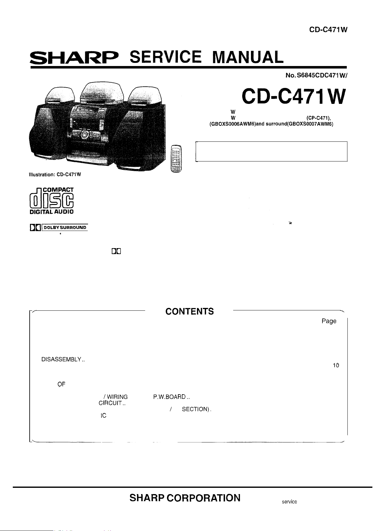
SERVICE MANUAL
PRO f LOGIC
Manufactured under license from Dolby Laboratories Licensing Corporation.
DOLBY, the double-D symbol
are trademarks of Dolby Laboratories Licensing Corporation.
and “PRO LOGIC”
W/
CD-C471
CD-C471
Speaker System.
l
In the interests of user-safety the set should be restored to its
original condition and only parts identical to those specified be
used.
mini component system consisting of
mini component system, front (CP-C471), senter
SAFETY
VOLTAGE SELECTION..
SPECIFICATIONS ............................................................................................................................................................
NAMES OF PARTS
OPERATION MANUAL
REMOVING AND REINSTALLING THE MAIN
ADJUSTMENT.. ..............................................................................................................................................................
NOTES ON SCHEMATIC DIAGRAM
TYPE
BLOCK DIAGRAM
SCHEMATIC DIAGRAM
WAVEFORMS OF
TROUBLESHOOTING (CD CHANGER CONTROL / CD SECTION). ............................................................................
FUNCTION TABLE OF
FL DISPLAY
REPLACEMENT PARTS LIST/EXPLODED VIEW
PRECAUTION FOR SERVICE MANUAL
TRANSISTOR AND LED
....................................................................................................................................................................
..................................................................................................................................................
..........................................................................................................................................................
.....................................................................................................................................................
.............................................................................................................................
................................................................................................................................
..........................................................................................................................................................
CD
..............................................................................................................................................
SIDE OF
...................................................................................................................................
..........................................................................................................
PARTS..................................................................................................
This document has been published to be used
for after sales
The contents are subject to change without notice.
only.
11
14
14
15
18
39
40
44
54
2
2
3
4
6
7
Page 2
CD-C471
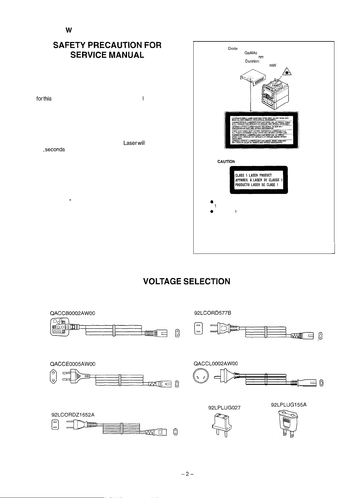
Precaution to be taken when replacing and servicing the
Laser Pickup.
The AEL (Accessible Emission Level) of Laser Power Output
model is specified to belowerthan Class
However, the following precautions must be observed during
servicing to protect your eyes against exposure to the Laser
beam
(1) When the cabinet has been removed, the power is turned
on without a compact disc, and the Pickup is on a position
outerthan the lead-in position, the Laserwill Iightforseveral
to detect a disc, Do not look into the Pickup Lens.
(2) The Laser Power Output of the Pickup inside the unit and
replacement service parts have already been adjusted prior
to shipping.
(3) No adjustment to the Laser Power should be attempted
when replacing or servicing the Pickup.
(4) Under no circumstances look directly into the Pickup Lens
at any time.
(5) CAUTION
Use of controls or adjustments, or performance
of procedures other than those specified herein may result
in hazardous radiation exposure.
Requirements.
Laser
This Mini Component System is classified as a CLASS
LASER product.
The CLASS
rear cover.
l
Use of controls, adjustments or performance of procedures other than those specified herein may result in hazardous radiation exposure.
As the laser beam used in this compact disc player is
harmful to the eyes, do not attempt to disassemble the
cabinet. Refer servicing to qualified personnel only.
Properties
Material:
Wavelength. 780
Emission
Laser Output:
LASER PRODUCT label is located on the
continuous
max. 0.6
The voltage selector is located on the AC voltage selector box. If adjustment is necessary, use a screwdriver in order to turn the
selector in either direction the correct voltage figure is displayed in the window next to the adjustment screw.
Figure 2 POWER SUPPLY CORD AND PLUG ADAPTOR
Page 3
FOR A COMPLETE DESCRIPTION OF THE OPERATION OF THIS UNIT, PLEASE REFER
TO THE OPERATION MANUAL.
CD-C471
Power source:
Power consumption:
Dimensions:
Weight:
Amplifier
Output power:
Input terminals:
Output terminals:
Type:
Signal readout:
Converter:
Frequency response:
Dynamic range:
AC 11
50160
112w
Width; 270 mm (1
Height; 303 mm (1 l-l
Depth; 350 mm
7.1 kg (15.3
PMPO; 1,000
Front speakers;
MPO; 176
(10
RMS; 80
(10
Center speaker;
MPO; 32
Surround speakers;
MPO; 32
Video/Auxiliary (audio signal)
500
Front speakers; 6 ohms
Center speakers; 4 ohms
Surround Speakers; 8 ohms
Headphones;
(recommended; 32 ohms)
Non-contact,
laser pickup
1 -bit D/A converter
20
90
V,
Hz
(total)
(88 88 W)
T.H.D.)
(40 40 W)
T.H.D.)
(10
(10
(10
(10
T.H.D.)
T.H.D.)
T.H.D.)
T.H.D.)
20
20
2;
kohms
ohms
multi-play compact disc player
20,000
Hz
semi-conductor
Type:
Frequency response:
Motor:
Signal/noise ratio:
Compact cassette tape
50
DC motor with electronic governor
55
50
Bias and erasure
system:
Tape speed:
Wow and flutter:
Heads:
AC
4.76
0.15
TAPE-l
TAPE-2: Record/playback
speaker
Type:
50 mm (2”) tweeter and super tweeter]
Maximum input power:
Impedance:
Dimensions:
80
6
Width; 200 mm
Height; 300 mm
Depth; 253 mm
Weight:
2.7 kg (5.8
l
Type:
Maximum input power: 40
Impedance:
Dimensions:
Weight:
100 mm (4”) full-range speaker
4
Width; 262 mm (1
Height; 145 mm
Depth; 201 mm
1.2 kg (2.6
14,000 Hz (Normal tape)
(TAPE 1, playback)
(TAPE 2, recording/playback)
(l-718 ips)
(WRMS)
Playback
1
Erase
1
type
mm
woofer,
ohms
6”)
ohms
6”)
6”)
1
l
l
Frequency range:
FM; 88
AM; 531
108 MHz
1,602
l
Type:
Maximum input power: 20
Impedance:
Dimensions:
Weight:
prior notice.
100 mm (4”) full-range speaker
8
ohms
Width; 170 mm
Height; 122 mm (4-l 3/l 6”)
Depth; 176 mm
0.7 kg (1.5
Page 4
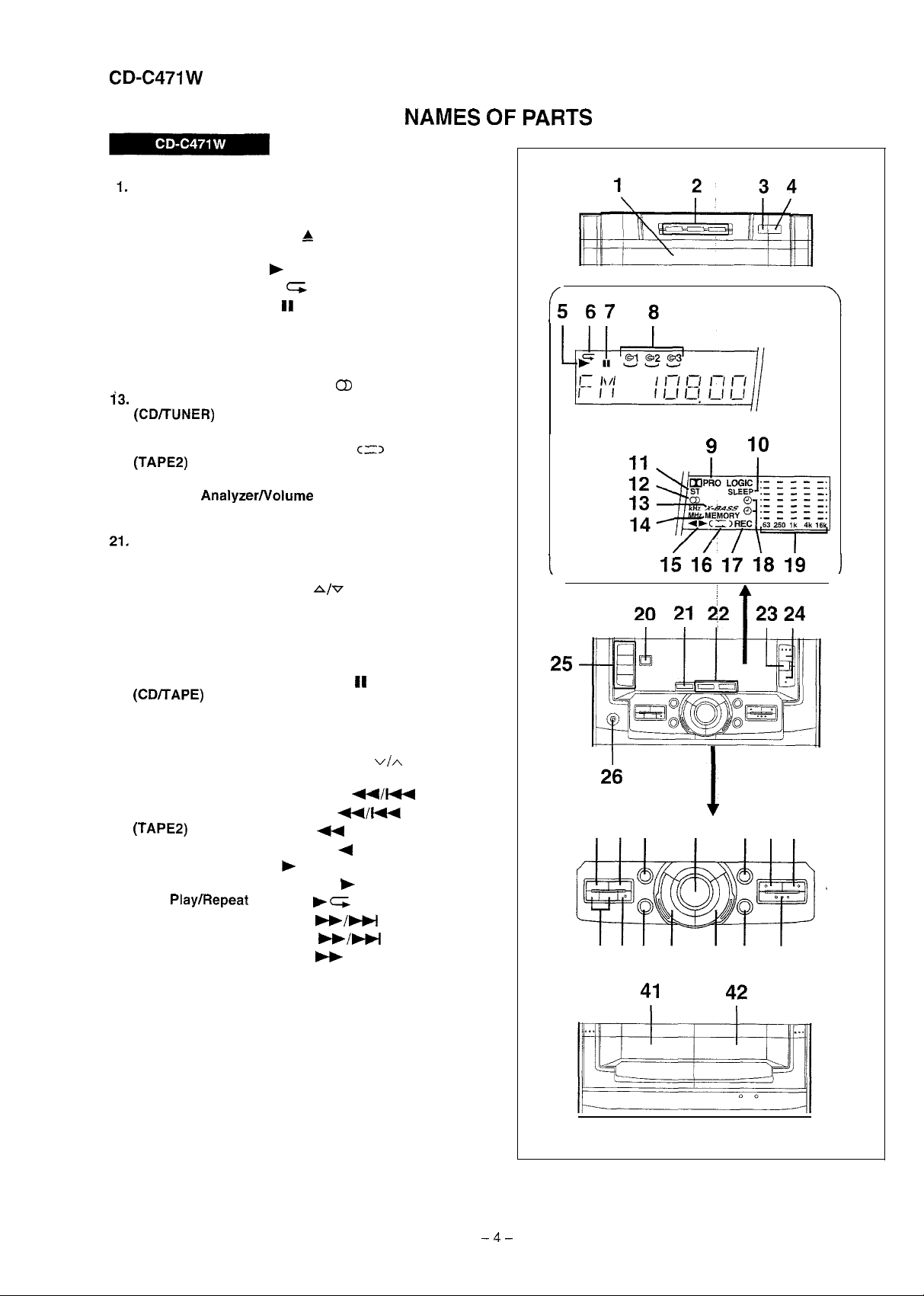
n
Front Panel
(CD) Disc Tray
2. (CD) Disc Number Select Buttons
3. (CD) Disc Skip Button
4. (CD) Open/Close Button:
5. (CD) Play Indicator:
6. (CD) Repeat Indicator:
7. (CD) Pause Indicator:
8. (CD) Disc Number Indicators
9. Dolby Pro Logic Indicator
10. Sleep Indicator
11. (TUNER) FM Stereo Mode Indicator: ST
12. (TUNER) FM Stereo Indicator:
Extra Bass Indicator: X-BASS
14. (CD/TUNER) Memory Indicator
15. (TAPE) Direction Indicators
16. (TAPES) Reverse Mode indicator:
17.
18. Timer Indicator
19. Spectrum AnalyzerNolume Level/Balance Indicator
20. On/Stand-by Button
Bypass Button
22. Center Mode Buttons: NORMAL/PHANTOM
23. Extra Bass Button: X-BASS
24. Volume Up/Down Buttons:
25. Function Selector Buttons
26. Headphone Socket
Record indicator
27. Clock Button
28. Timer/Sleep Button
29. (TAPES) Record Pause Button:
30. (CD/TAPE) Stop Button:
31. Equalizer Selector/Demo Mode Button
32. CD Edit Button
33. Tape 1 Edit Button
34. Tuning and Time Up/Down Buttons: ,,/,..,
35. Memory/Set Button
36. (CD) Track Down/Review Button:
(TUNER) Preset Down Button:
Fast Wind Button:
37. (TAPE 2) Reverse Play Button:
38. (TAPE 1) Play Button:
(TAPE 2) Forward Play Button:
(CD) Play/Repeat Button:
39. (CD) Track Up/Cue Button:
(TUNER) Preset Up Button:
(TAPE2) Fast Wind Button:
40. (TAPES) Reverse Mode Button
41. (TAPE 1) Cassette Compartment
42. (TAPE 2) Cassette Compartment
l
n
27 28 29
30
3132 33
3435 36 37 38 39 40
Page 5
n
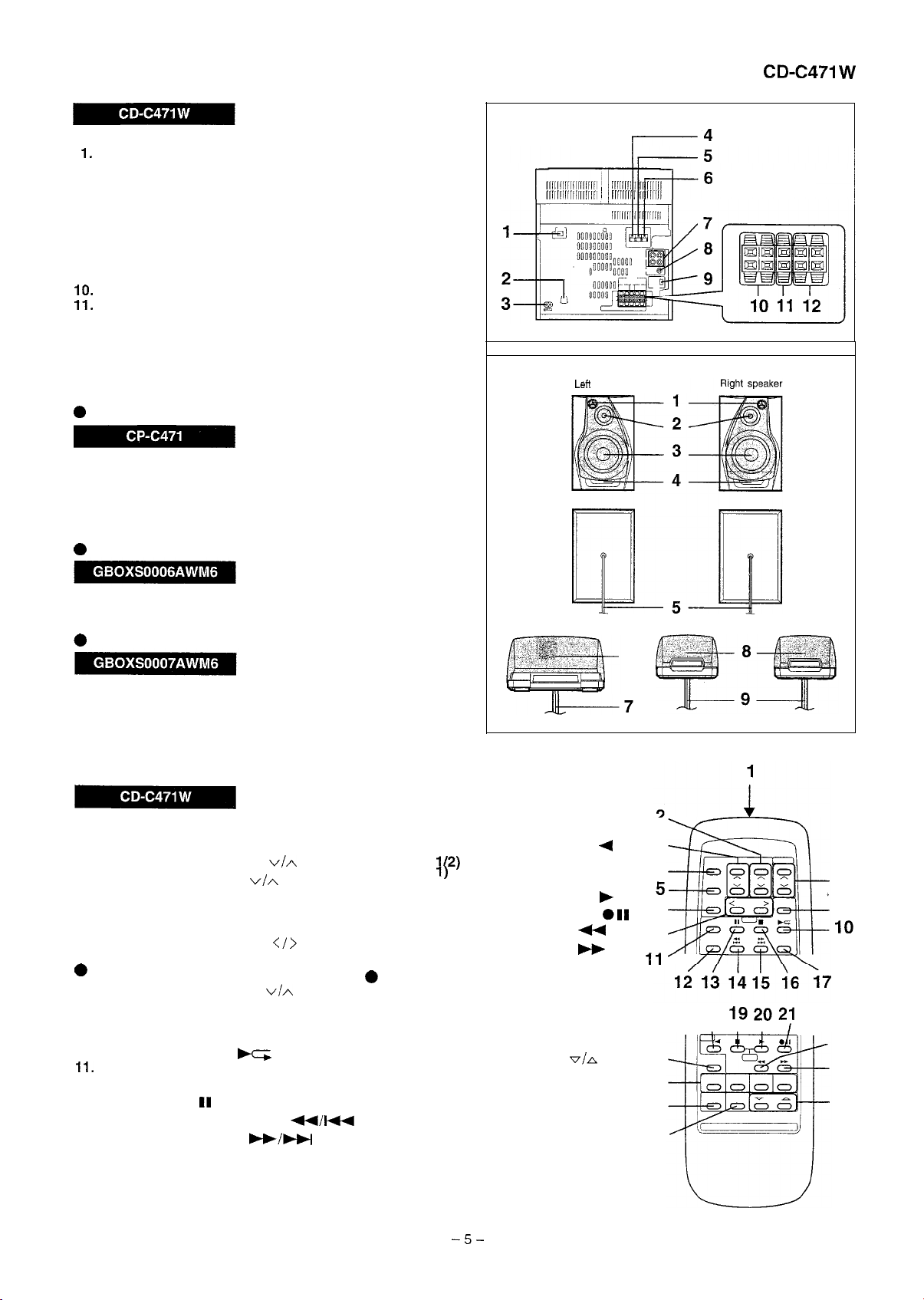
Rear Panel
CD Digital Output Socket
2. AC Voltage Selector
3. AC Power Input Socket
4. AM Aerial Terminal
5. Aerial Earth Terminal
6. FM 75 Ohms Aerial Terminal
7. Video/Auxiliary (Audio Signal) Input Sockets
8. Sub Woofer Output Socket
9. Span Selector Switch
Front Speaker Terminals
Center Speaker Terminals
12. Surround Speaker Terminals
I I
I
n
Speaker Section
Front Speaker
1. Super Tweeter
2. Tweeter
3. Woofer
4. Bass Reflax Duct
5. Speaker Wire
Center
6. Full-Range Speaker
7. Speaker Wire
Surround
8. Full-Range Speaker
9. Speaker Wire
n
1. Remote Control Transmitter LED
2. Surround Level Buttons:
3. Center Level Buttons:
4. Dolby Pro Logic Button
5. Center Mode Button
6. Test Tone Button
7. Balance Control Buttons:
Tuner control section
8. Preset Up/Down Button:
l
9. Disc Skip Button
10. Play/Repeat Button:
Memory Button
12. Clear Button
13. Pause Button:
14. Track Down/Review Button:
15. Track Up/Cue Button:
16. Stop Button:
17. Random Button
Speaker
Speaker
Remote Control
CD Control section
q
l
Tape control section
18. (TAPE 2) Reverse Play Button:
19. (TAPE
(TAPE
20.
(TAPE 2) Forward Play Button:
(TAPE2)Record Pause Button:
21.
(TAPE2)Fast Wind Button:
22.
23. (TAPE 2) Fast Wind Button:
Common section
24. Equalizer Mode Button
25. Function Selector Buttons
26. On/Stand-by Button
27. Extra Bass Button: X-BASS
28. Volume Up/Down Buttons:
Stop Button:
Play Button/
n
speaker
6
3
4
6
8
9
7
18
I I I
22
24
23
25
26
28
27
Page 6
example,
TUNING/’
TIME
set for
SET
Press
ON/STAND-BY
Press
CLOCK
seconds, press the MEMORY/SET
Press
TUNINGmIME
The 24.hour display
The
The 12-hour
Note that this
Press
Press
time
When the 12.hour display
Press
l
5-minute intervals.
The
Press
l
l event
disconnected,
this
reset (see page
MEMORY/SET
Press for more
MEMORY/SET
for at least 0.5 seconds to change
MEMORY/SET
a power failure or when
AC power
off
indicate
the AC power
follow
to enter
23:59)
display
set
or
not advance even
clock display
or
selected, “AM” will
F.
button to adjust the
is restored,
time when
was disconnected.
procedure below to change
stand-by
to select
appear.
first
to
once to advance
seconds
minutes advance
AC power
clock display
power failure
time
auto-
time
l
l
l
l
l
l display correct.
l operation correct.
l
batteries operating distance becomes
or
operation becomes erratic.
sensor
the main
sensor
operation. Change
vibrations.
microcomputer
stored memory contents (clock
tuner
tuner preset memory see “To erase
ON/STAND-BY
soft
the
following conditions:
CD presets).
to enter
VOLUME
down
strong
ON/STAND-BY
remote control
or
direction
stand-by
may
timer
TUN-
for
l
Perlorm
demonstration
DEMO
to enter
MEMORY/SET
CLOCK
above.
above.
clock
MEMORY/SET
press
CLOCK
l
Press
ON/STAND-BY
Whilst
second.
Periorm steps
l
down
clock
appear for about
enter
VOLUME
down the ON/STAND-BY
above.
erase
timer
seconds
stand-by
TUN-
data stored
tuner
for
CD
Page 7
Caution on Disassembly
Follow the below-mentioned notes when disassembling
the unit and reassembling it, to keep it safe and ensure
excellent performance:
Take cassette tape and compact disc out of the unit.
2. Be sure to remove the power supply plug from the wall
outlet before starting to disassemble the unit.
3. Take off nylon bands or wire holders where they need to
be removed when disassembling the unit. Afterservicing
the unit, be sure to rearrange the leads where they were
before disassembling.
4. Take suffcient care on static electricity of integrated
circuits and other circuits when servicing.
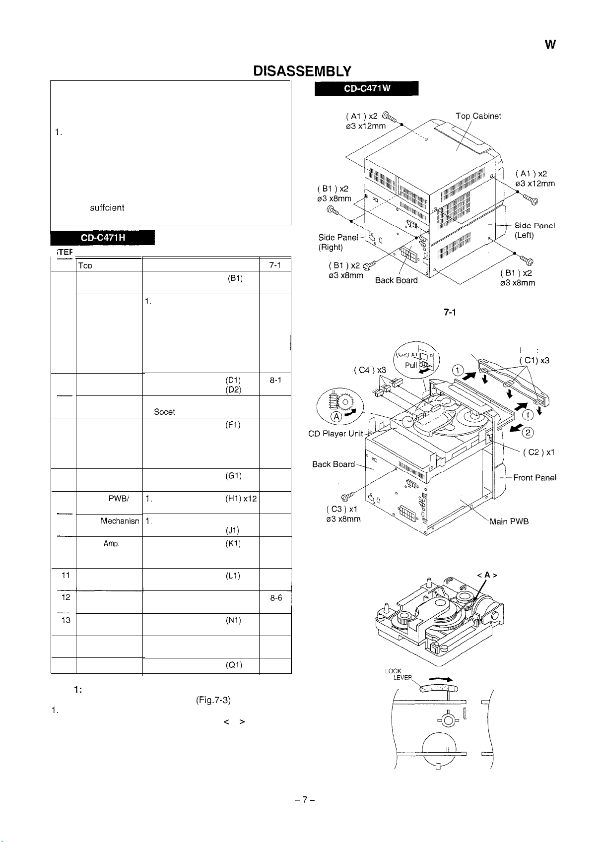
CD-C471 W
REMOVAL
1
2
3
45Back Board
6
7
8
9
10
14
15
Cabinet
Side Panel
(Left/right)
CD Player Unit/
CD Tray Cover
Tuner PWB
Main PWB
Front Panel
Display
Switch PWB
Tape
Power
CD Servo PWB
Turntable
CD Player Base
CD Changer
Mechanism
CD Mechanism
PROCEDURE
1. Screw .....................
1. Screw .....................
Turn on the power supply,
open the disc tray, take out
the CD cover, and close.
(Note 1)
2. Hook ......................
3. Hook ...................... (C2) x2
4.
Screw ....................
5.
Socket ...................
1. Screw ....................
2.
Socket ...................
1. Screw ....................
2.
1.
Screw ....................
2. Socket ................... (F2) x2
3.
Flat Wire................ (F3) x2
4.
Tip Wire.................
5.
Socket ...................
1. Screw ....................
2.
Hook...................... (G2) x2
Screw ....................
Open the cassette holder.
2. Screw ....................
1. Screw ....................
PWE
2.
Socket ................... (K2) x2
3. Push Rivet ............ (K3) x4
1. Screw ....................
2. Cover .................... (L2) x4
1. Screw ....................
2.
Cover ....................
1. Screw ....................
2. Guide .................... (N2) x2
1. Screw ....................
1. Screw ....................
FIGURE
(Al) x4
x6
7-l
7-2
(Cl) x3
(C3) xl
(C4) x3
x13
xl
(El) xl 8-l
(E2) xl
xl
(F4) xl
(F5) xl
x5
x4
xl
(Ml) xl
(M2)
(Pl) x4
x2
xl
x2
xl
a-2
8-2
a-3
a-3
8-4
8-5
8-6
8-7
8-7
Figure
CD Tray Cover
Figure 7-2
Hook
Note
How to open the changer manually. (Fig.7-3)
Insert the tip of fine screwdriver into the hole of CD player
base, and press down the worm wheel c A
2. Then, turn fully the lock lever in the arrow direction through
the hole on the loading chassis bottom in this state.
After that, push forward the CD player base.
Figure 7-3
Page 8
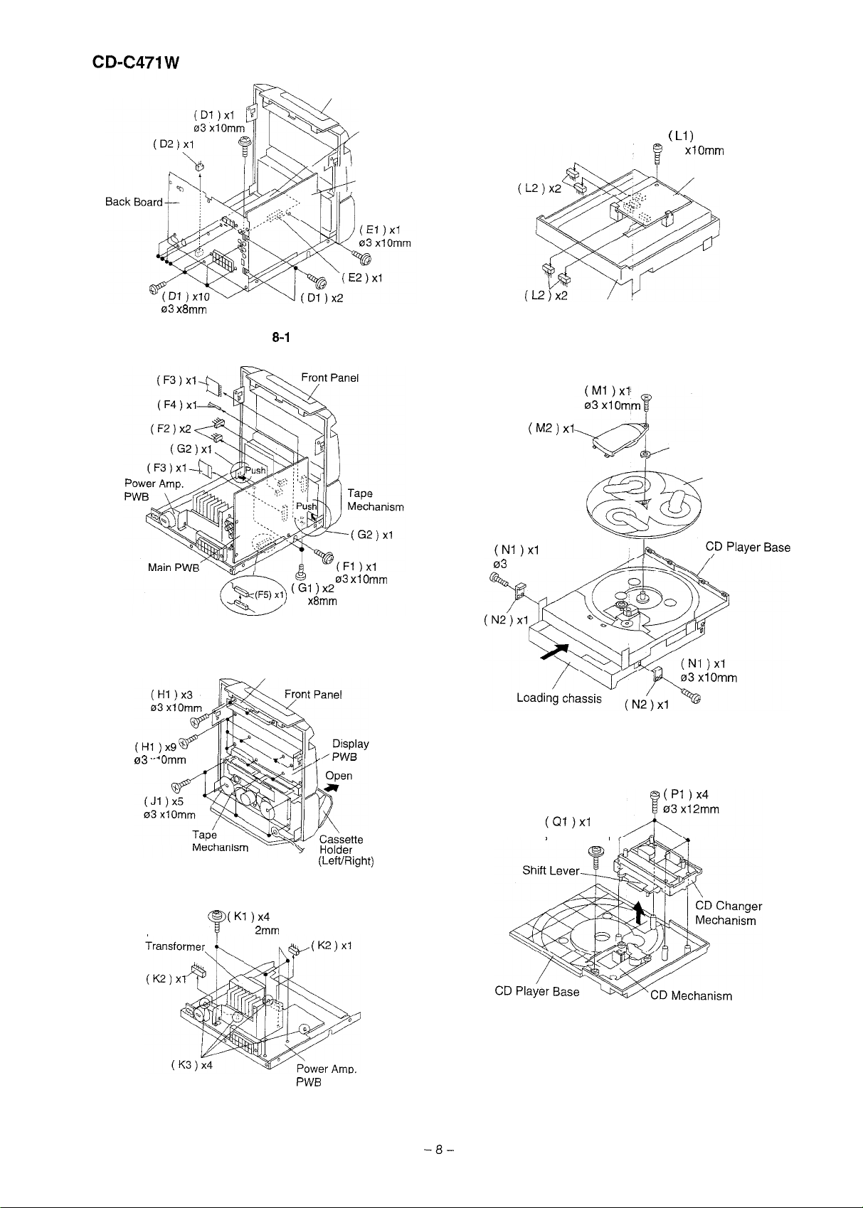
Front Panel
Tuner
PWB
Main PWB
Figure
03 xl Omm
Loading Chassis
Figure 8-5
I
Li
xl
03 xlOmm
CD Servo PWB
Washer
Turntable
xl
Power
Figure 8-2
Switch PWB
Figure 8-3
03 xl
03
xl Omm
Figure 8-6
02.6 xl Omm
Figure 8-4
Be careful when installing the CD changer mechanism.
Install the CD changer mechanism on the CD player base after
the shift lever has been set in the highest position.
Figure 8-7
Page 9
CD-C471
Note:
The center and SURROUND speakers can be easily disas-
sembled. Therefore the disassembling method is not discribed.
For details refer to the disassembling drawing in the Parts
Guide.
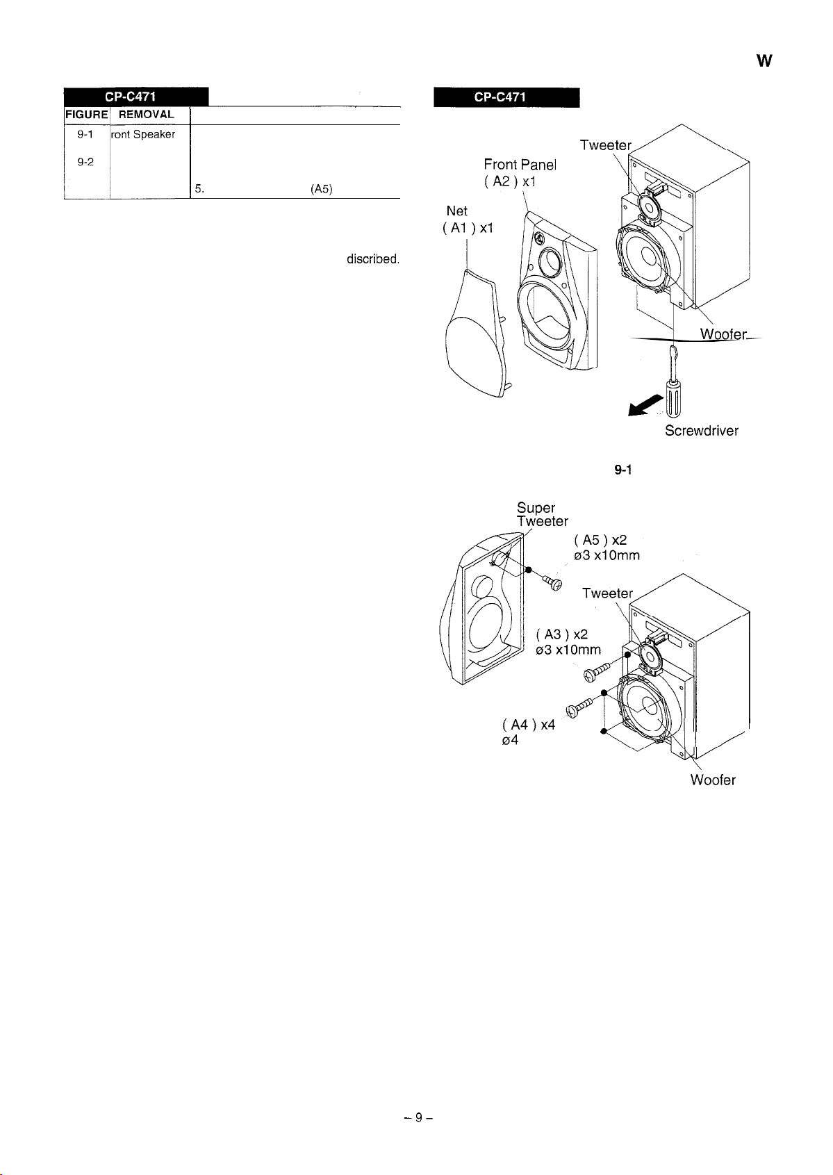
PROCEDURE
1
Net
..........................
2. Fromt Panel
3.
Screw ..................... (A3) x2
4. Screw ..................... (A4) x4
Screw .....................
...........
(Al) xl
(A2) xl
Figure
xi 4mm
I
Figure 9-2
Page 10
CD-C471
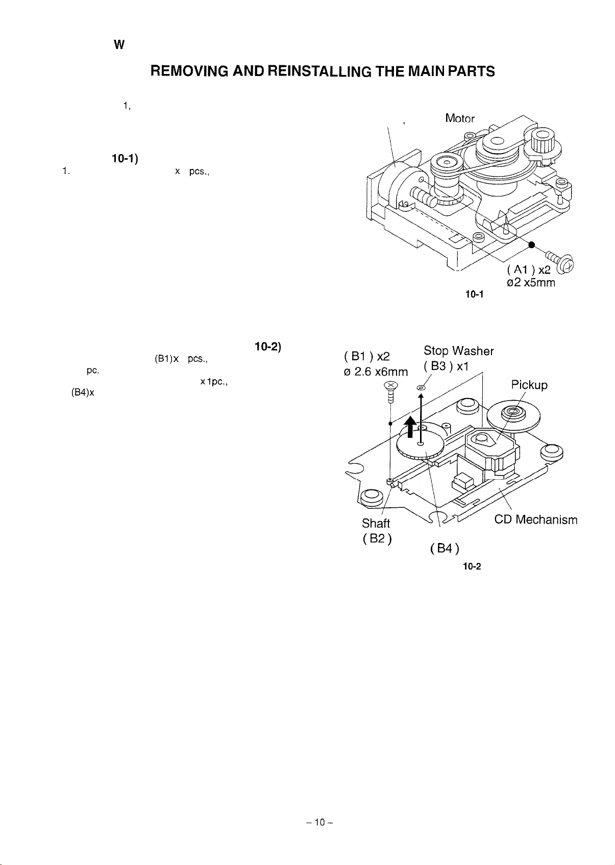
CD MECHANISM SECTION
Perform steps
to remove the CD mechanism.
How to remove the turntable up/down motor
(See Fig.
Remove the screws (Al) x 2
up/down motor.
How to remove the pickup (See Fig.
1. Remove the screws
xl
2. Remove the stop washer (B3) x to remove the gear
1 pc.
3. Remove the pickup.
2, 3, 14 and 15 of the disassembly method
to remove the turntable
x 2
to remove the shaft (B2)
Turntable Up/Down
Figure 10-l
xl
Gear
Figure
xl
Page 11
CD-C471
MECHANISM SECTION
l
Driving Force Check
Torque Meter
Play: TW-2412
l
Torque Check
Torque Meter Specified Value
Play: TW-2111
Fast forward: TW-2231
Rewind: TW-2231
l
Tape Speed
Test Tape
Normal
11
speed
Tape 1: Over 80
Tape 2: Over 80
Tape 1
30 to 60
Adjusting
cm
Point
3,000
Specified Value
Tape 2
30 to 100
50 to 100
50 to 100
Specified Instrument
Value
Connection
Speaker
Hz
terminal
TUNER SECTION
Low-range frequency
High-renge frequency
l
AM IF/RF
Signal generator: 400 Hz,
Test Stage Frequency Frequency
IF
AM Band
Coverage
AM
990
Tracking
Input: Antenna, Output: TP302
Input: Antenna, Output:
Notes:
1: Description of the “FM IF Adjustment” is not carried on this
Manual. It is because the IF coil in the FM front end section
has been best adjusted in the factory so that its further
adjustment is not needed at the field. When replacing the
FM front end assembly, no adjustment is needed either.
2: The parts in the FM front end section are prepared in a
complete unit, so you can’t obtain each part individually
FM Mute Level
Signal generator: 1
Display
1,602
531
40
AM modulated
Adjusting Connection
Parts
T306
1.1
0.1
T302
dev., FM modulated
TAPE MECHANISM PWB
T351
T306
TUNER PWB
I
ANTENNA
TERMINAL
AM BAND
COVERAGE
Figure 11 ADJUSTMENT POINTS
AM
TRACKING
Page 12
CD-C471
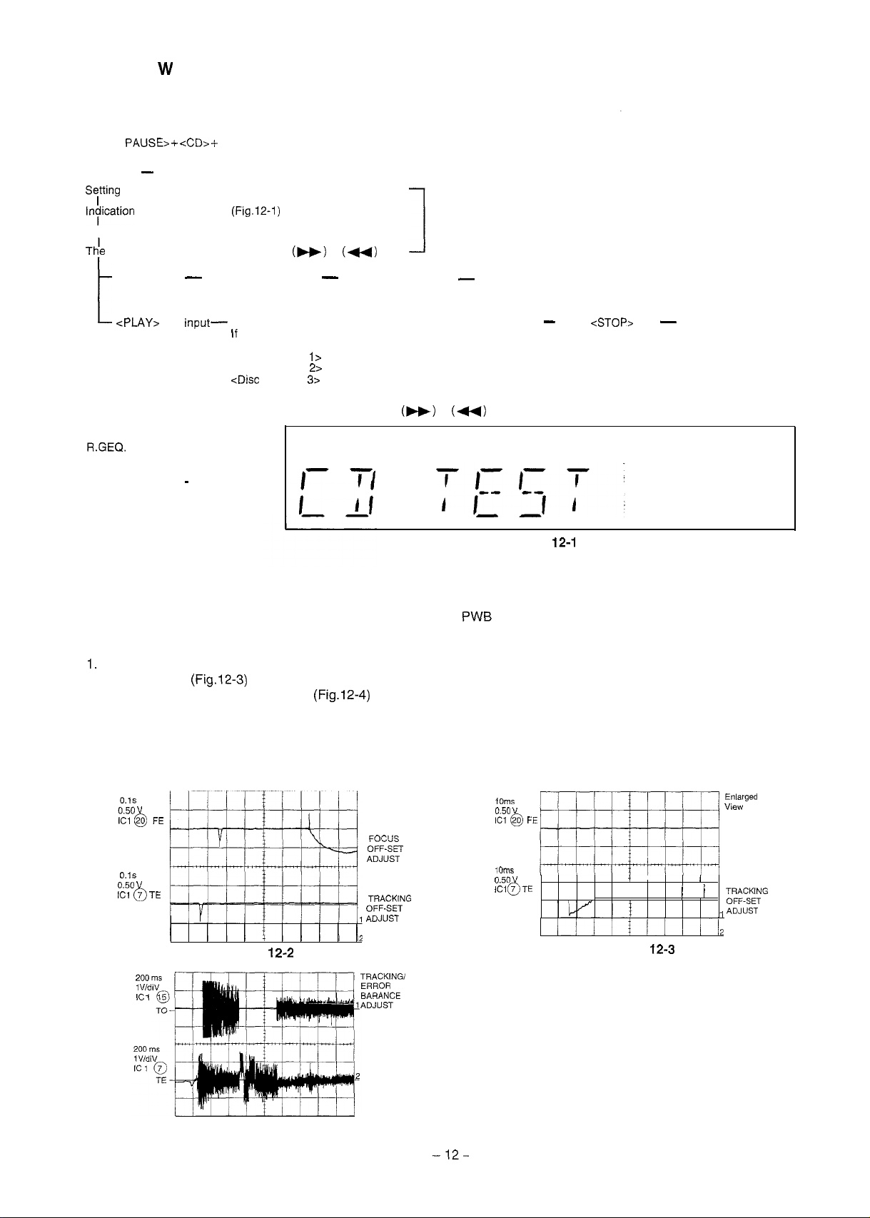
TEST MODE
l
Setting the test mode
Any one of test mode can be set by pressing several keys as follows.
<REC.
l
TEST
Function
of TEST mode
OPEN/CLOSE operation is manual operation.
pickup can be moved by using the
<MEMORY>
LASER ON
<POWER>
mode
CD test
mode
of CD TST mode (Fig.l2-1)
<MEMORY>
Tracking on the spot.
SERVO OFF PLAY
TEST: CD operation test
IL is not performed.
or
key.
<MEMORY>
Tracking on the spot.
SERVO ON PLAY
<STOP>
STOP
key
TOC. IL is performed, and the ordinary PLAY is performed.
the following key is pressed during PLAY, it is possible
to specify directly any Track No.
<Disc Number
<Disc Number
Number
key: Track 4
key: Track 9
key: Track 15
Press
key.
Stop
Note:
Only in STOP state it is possible to slide the pickup with the
VOL. --- Last memory
BAL. --- CENTER
--- FLAT
X-BAS --- OFF
Canceling method
POWER OFF
or
key.
I
Figure
CD SECTION
Since this CD system incorporates the following automatic adjustment function, when the pickup is replaced, it is not necessary
to readjust it.
Since this CD unit does not need adjustment, the combination of
l
Automatic adjustment item
Focus offset (Fig.1 2-2)
2. Tracking offset
3. E/F balance (tracking error balance) (Fig.12-4)
4. RF level AGC function (HF level: constant)
5. RF level automatic follow-up of the tracking gain
and laser pickup unit is not restricted.
This automatic adjustment is performed each time a disc is changed. Therefore,
each disc is played back using the optimal settings.
Figure
Figure 12-4
Figure
TRACKING
Page 13
CD-C471
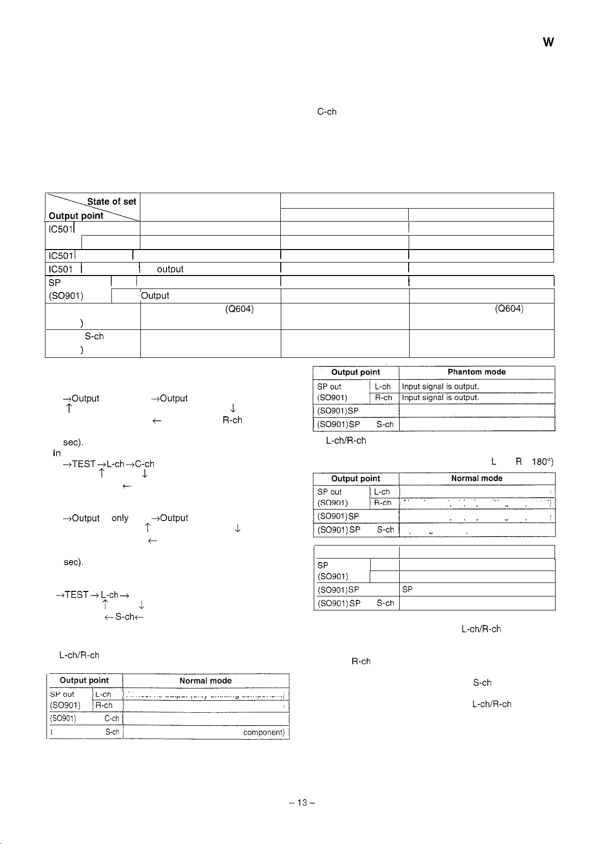
EXPLANATION OF DOLBY SURROUND PRO LOGIC AND EVALUATION METHOD
Outline
l
l
Namely, two speakers are connected in parallel to one
amplifier.
l
In the Pro Logic BYPASS mode the amplifierfor C-ch (center
channel) and the amplifier for S-ch (surround channel) are in
MUTE state. The SP output is cut.
l
State of element output and terminal output in specific mode
In the normal mode of Pro Logic ON mode the amplifiers for
and S-ch are in operative state, so that the SP output
appears.
l
In the Phantom mode of Pro Logic ON mode the amplifier for
C-ch is in MUTE state, so that the SP output is cut. The
amplifier for S-ch (surround) is in operative state, so that the
SP output appears
Dolby Pro Logic
Bypass mode
12 pin L-out Output enabled state
11 pin R-out Output enabled state
9 pin C-out
10 pin S-out
OUT
No output
No
L-ch
Output enabled state
R-ch ,Output enabled state
SP OUT C-ch
No output in MUTE
state Output enabled state
(SO901
SP OUT
No output in MUTE (Q603) state
(SO901
Test tone output
l
Pro Logic ON Normal mode
Press the remote control TEST TONE button.
of only L-ch
Output of only S-ch
of only C-ch
Output of only
The test tone (noise) is repeatedly output for output period
(2 set).
this case the following indication appears repeatedly.
S-ch
R-ch
l
Pro Logic ON Phantom mode
Press the remote control TEST TONE button.
of only L-ch
of only R-ch
Output of only S-ch
The test tone (noise) is repeatedly output for output period
(2
In this case the following indication appears repeatedly.
R-ch
Relation between VIDEO IN input and output in Pro Logic
ON state
(1)
same phase input into VIDEO IN input jack in
VIDEO Function mode
Dolby Pro Logic On mode
Normal mode
Output enabled state
Output enabled state
Output enabled state
Output enabled state
Output enabled state
Output enabled state
Output enabled state
out C-ch
out
(2)
reverse phase input into VIDEO IN input jack in
VIDEO Function mode
(Reverse phase: Phase difference between
out C-ch
out
Output point
out
out C-ch
out
l
Accordingly, if you want to output signal waveform to C-ch SP
out, give the same phase input into
Pro Logic Normal mode.
If one of channels receives input, C-ch does not output. Only
L-ch or
outputs.
Phantom mode
Output enabled state
Output enabled state
No output
Output enabled state
I
Output enabled state
Output enabled state
No output in MUTE
state
Output enabled state
SP cut, no output
and
is
Almost no output (only omitting component)
Almost no output (only omitting component)
Almost no output (only omitting component)
Input signal is output.
Phantom mode
L-ch
Almost no output (only omitting component)
R-ch Almost no output (only omitting component)
cut, no output
INPUT in the
SP out
(50901) SP out
Almost no output (only omitting component)
Almost no output (only omitting component)
Input signal is output.
Almost no output (only omitting
l
If you want to output signal waveform to
SP out, you can
use either Normal mode or Phantom mode. However, 180”
reverse phase input must be given to
INPUT.
Page 14
CD-C471 W
l
Resistor:
To differentiate the units of resistors, such symbol as
are used: the symbol
means 1000 ohm and the symbol
means 1000 kohm and the resistor without any symbol is
ohm-type resistor. Besides, the one with “Fusible” is a fuse
l
Capacitor:
To indicate the unit of capacitor, a symbol
symbol
means micro-micro-farad and the unit of the
is used: this
capacitor without such a symbol is microfarad. As to
electrolytic capacitor, the expression “capacitance/withstand
voltage” is used.
(CH), (TH),
(UJ): Temperature compensation
(ML): Mylar type
(P.P.): Polypropylene type
l
Schematic diagram and Wiring Side of
model are subject to change for improvement without prior
notice.
REF. NO DESCRIPTION
OPEN/CLOSE
and
for this
POSITION
l
The indicated voltage in each section is the one measured
by Digital Multimeter between such a section and the chassis with no signal given.
1. In the tuner section,
indicates AM
2. In the main section, a tape is being played back.
3. in the deck section, a tape is being played back.
indicates the record state.
4. In the power section, a tape is being played back.
5. In the CD section, the CD is stopped.
l
Parts marked with
maintaining the safety of the set. Be sure to replace these
parts with specified ones for maintaining the safety and
performance of the set.
are important for
SW712
SW718
SW721
SW723
TAPE
CENTER MODE/PHANTOM
CENTER MODE/NORMAL
DOLBY PRO LOGIC BYPASS
REC PAUSE
ECB
268 GR
Y
KTC3203
SW801
VOLTAGE SELECTOR
SWM 3 REC FWD
REC RVS
SWM 5 F.A.S.
SWM 6 CAM
Figure 18 TYPES OF TRANSISTOR AND LED
110-127-
Page 15
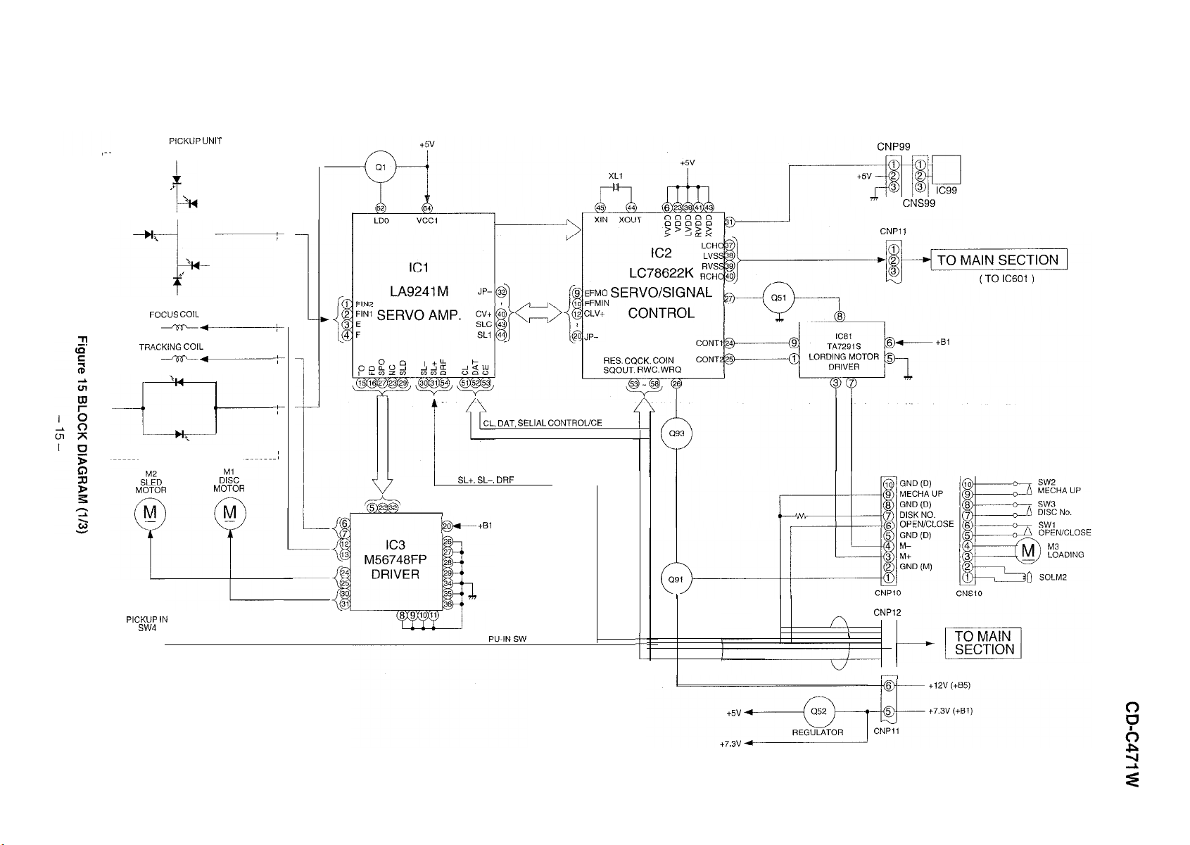
COIL
SL-.
SELIAL CONTROUCE
DIGITAL
OUT
Page 16
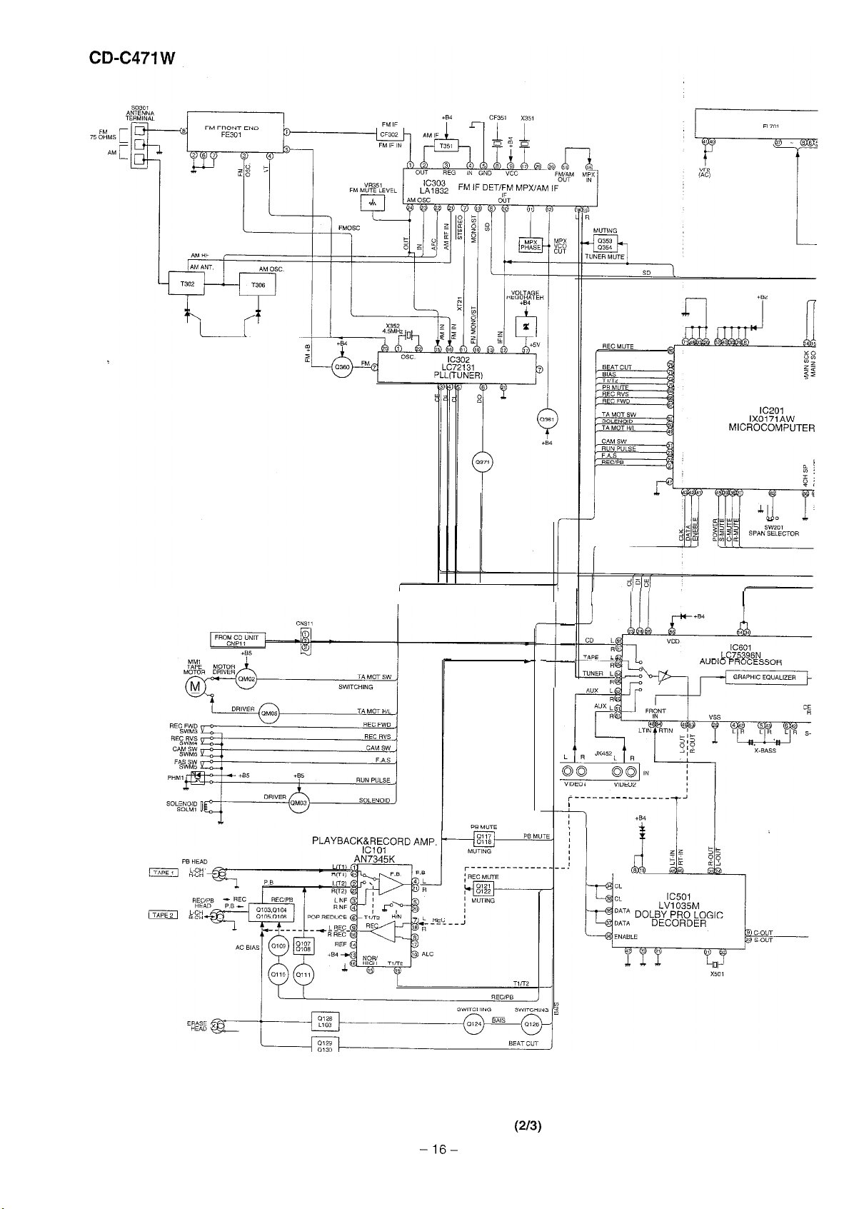
Figure 16 BLOCK DIAGRAM
Page 17
CD-C471
Figure 17 BLOCK DIAGRAM
Page 18
CD-C471
I
PICKUP UNIT
---------
---
l
The numbers
l
NOTES ON SCHEMATIC DIAGRAM can be found on page 14.
1
to
are waveform numbers shown in page 39.
Figure 18 SCHEMATIC DIAGRAM
4
Page 19
CD SIGNAL
CD-C471
CD SIGNAL
7
Figure 19 SCHEMATIC DIAGRAM (Z/l 3)
9
10
11
12
Page 20
CD-C471
l
NOTES ON SCHEMATIC DIAGRAM can be found on page 14.
1
2
3
Figure 20 SCHEMATIC DIAGRAM
20
4
5
Page 21
FM SIGNAL
PLAYBACK SIGNAL
RECORD SIGNAL
CD SIGNAL
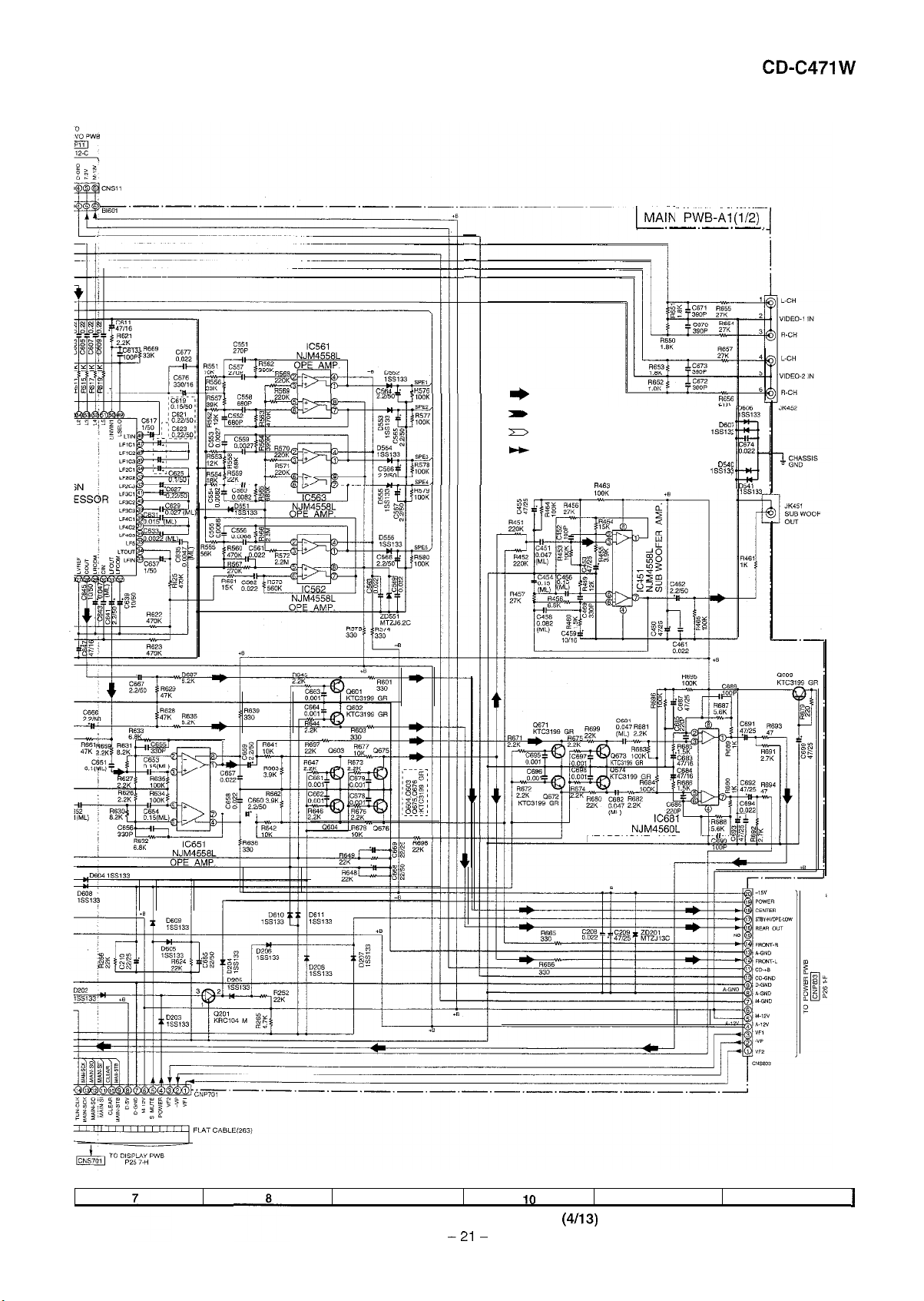
MAIN PWB-A1(1/2)
9
Figure 21 SCHEMATIC DIAGRAM
HEADPHONE AMP.
11
12
Page 22
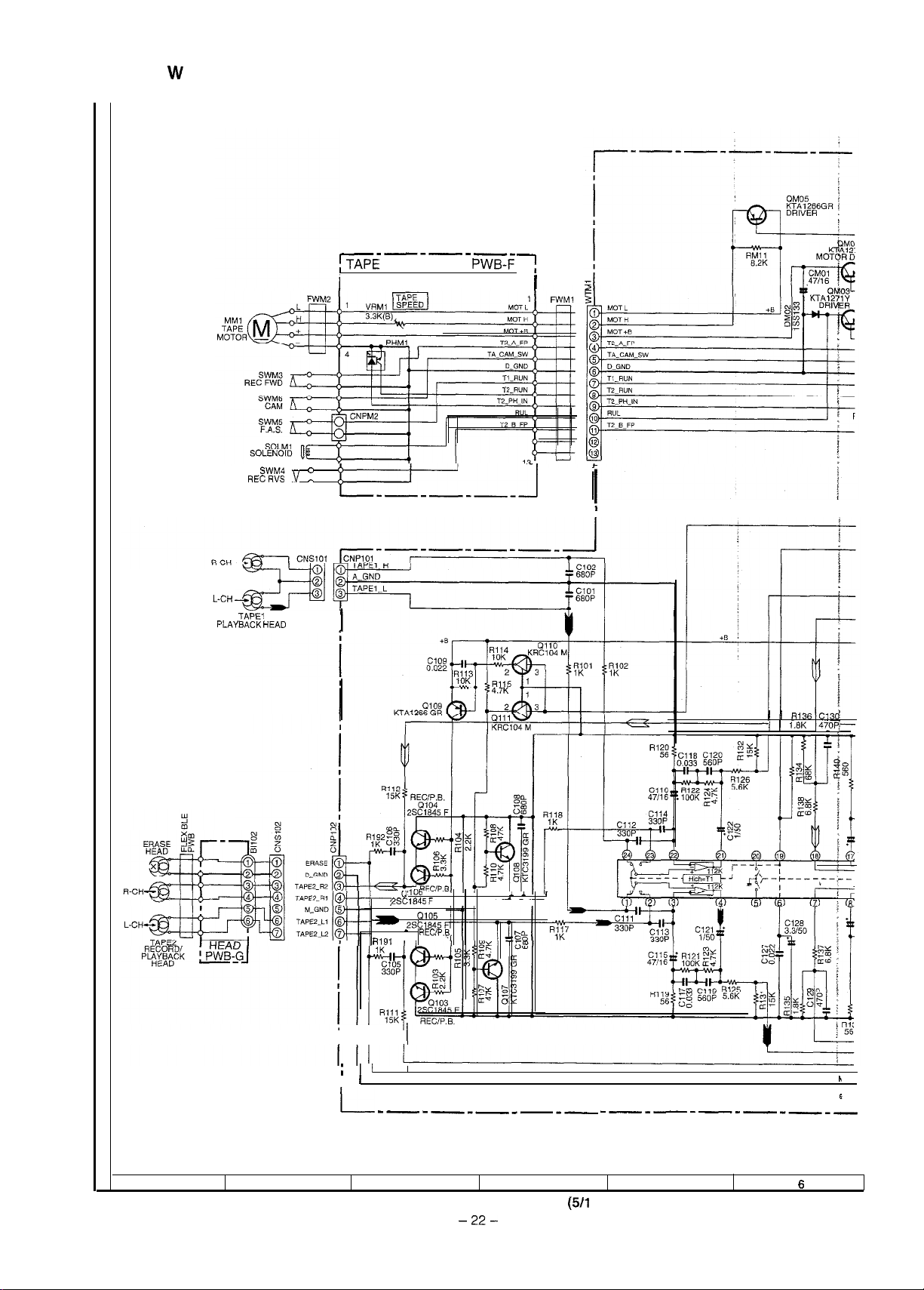
CD-C471
MECHANISM
I
ill
I
RECIP.6.
l
NOTES ON SCHEMATIC DIAGRAM can be found on page 14.
1
2
3
Figure 22 SCHEMATIC DIAGRAM
4
5
3)
Page 23

CD-C471
7 8
GR
9
10
Figure 23 SCHEMATIC DIAGRAM
23
12
Page 24

CD-C471
A
FL701
SYSTEM MICROCOMPUTER
l
NOTES ON SCHEMATIC DIAGRAM can be found on page 14.
1
2
Figure 24 SCHEMATIC DIAGRAM
3
24
4
3)
5
6
Page 25

CD-C471
IOK
10K
DISC2
DISC3
LED716
LED714
DISPLAY PWB-A3
,
1
,
INPUT/OUTPUT EXPANDER
1K
1K
LED701
REW
FF
PLAY
7
9
10
11
12
Figure 25 SCHEMATIC DIAGRAM
25
Page 26

CD-C471
A
STK40704
POWER AMP.
l
NOTES ON SCHEMATIC DIAGRAM can be found on page 14.
2
3 4
Figure 26 SCHEMATIC DIAGRAM
26
3)
5
6
Page 27

CD-C471
SIGNAL
MIN.
LA4450
POWER AMP.
f
I-
9
10
Figure 27 SCHEMATIC DIAGRAM (10113)
27
11
Page 28

CD-C471 W
ANTENNA
750hms
CHASSIS
GND
CHASSIS
GND
AM
GND
FM
I
FE301
FM FRONTEND
I
I
I
I
SIGNAL
SIGNAL
* NOTES ON SCHEMATIC DIAGRAM can be found on page 14.
1
Figure 28 SCHEMATIC DIAGRAM (1
28
I
Page 29

CD-C471
I
I
I
I
I
I
I
I
.
266
a
D351
ZD352
MTZJ3.9B
KRC107
MPX PHASE
22K
MTZJ5.1
I
I
I
I
I
I
I
I
I
I
I
I
I
II
I
I
I
I
I
7
a
Figure 29 SCHEMATIC DIAGRAM
9
29
11
12 I
Page 30

CD-C471
NORMAL
2
3
Figure 30 SCHEMATIC DIAGRAM
4
3)
5
6
30
Page 31

DISPLAY PWB-A2
CD-C471 W
PWB-A3
7 8
9
Figure 31 WIRING SIDE OF
-31
11
12
I
Page 32

CD-C471 W
TUNER
1
2
Figure 32 WIRING SIDE OF
3
4 5
6
32
Page 33

CD-C471 W
SELECTOR
7 8
9
Figure 33 WIRING SIDE OF
33
WH(W)
WHITE
BK
BLACK
PK
PINK
10
11
12
Page 34

MAIN
TAPE MOTOR
PICKUP
-,_,
l
The numbers
to
are waveform numbers shown in page 39.
2
3
Figure 34 WIRING SIDE OF
34
JACK
I
4
I
6
Page 35

CD-C471
UP/DOWN LOADING
7
Figure 35 WIRING SIDE OF
9
10
11
12
35
Page 36

1
2
Figure 36 WIRING SIDE OF
3
4
5
6
36
Page 37

CD-C471 W
7
a
Figure 37 WIRING SIDE OF
9
11
12
I
Page 38

CD-C471 W
Figure 38 WIRING SIDE OF
38
ANTENNA
Page 39

CD-C471
.oo
5.0 v
WAVEFORMS
OF CD CIRCUIT
I
00
Page 40

CD-C471
TROUBLESHOOTING (CD SECTION)
When the CD does not function
When the CD section does not operate When the objective lens of the optical pickup is dirty,this section may not operate.Clean
the objective lens,and check the playback operation.When this section does not operate even after the above step is taken,check
the following items.
Remove the cabinet and follow the troubleshooting instructions.
and/or no
Before attempting any adjustment make certain that the lens is clean. If not, clean it as mentioned below.”
Turn the power off.
Gently clean the lens with a lens cleaning tissue and a small amount of isopropyl alcohol.
Do not touch the lens with the bare hand.
Is
5
till OV down pulse (approx. 300 ms) input
Of Contents) may be caused by build up of dust other foreign matter on the laser pickup lens.
Check the SW3 and the wiring from the
pin 54 to the
into the
Is there following voltage input on the
specific state?
When the CD mechanism is moved up: OV
In other states:
Check
Is there following voltage input on the
specific state?
When the CD mechanism is moved up: OV
In other states:
pin 54 when the turntable is rotating?
I
Yes
pin 54 in the
Yes
pin26 Q9l and Q93 and the periphery.
pin 54 in the
Check the SW2 MECHA UP SW and the wiring from the
No
pin 21 to the SW2 MECHA UP SW.
Check the SW2 MECHA UP SW and the wiring from the
pin 54 to the SW2 MECHA UP SW.
Yes
Is
output from the
switch is pressed?
output from the
above?
Check turntable motor and turntable mechanism.
pin 26 during SEC when the disc skip
Yes
emitter during operation stated
Yes
40
Check the wiring of
Check
and the periphery.
pin 26 and Q93 BASE.
OK
defective.
Page 41

Wheri the CD tray fails to open
CD-C471
Is there following voltage input in specific state of
Open state: OV
Close state: OV
Intermediate state between open state and close state:
I
Yes
Is
output to
CLOSE key is
Is
output between
stated above?
Check the loading motor (M3) and the loading mechanism.
The CD
pin 24
is defective. Replace it.
pins 3 and 7 during operation
Yes
kevs don’t work.
pin
Check the OPEN CLOSE SW and the wiring from the
No
No
pin 53 to the OPEN CLOSE SW.
Check the wiring of the
Check the periphery of
pins 24 and 25,
I
OK
pins 1 and 3.
Yes
Check the CD,
reset terminal.
See if the pick-up is in the PICKUP IN SW position.
If the items mentioned above are OK, check the main
microcomputer
Check the Focus
Playback can be performed without a disc.
Does the pick-up move
power supply, and 16.93 MHz clock, and
Yes
HF system.
0.50 v
FD
0.50
Focus search OK
Figure 41
No
Does the output waveform
Fig.
I
Check the microcomputer data on pins
Check the area around
Page 42

CD-C471 W
Playback can only be performed when,a disc is
loaded.
. .
Is the Focus servo active? (Can you hear it working?)
Yes
Yes
Is HF waveform normal (see the Fig.
Yes
Check the tracking system.
Hi
(When playing
back the disc)
Figure
l
--
No
No
ICI
Check the laser diode driver.
Check the area around ICl(16)
If the disc is not turning, the DRF
should not change to
Waveform is unstable.
0.5s
v
FD
0.55
v
10.0
ICI
DRF
2.00
@TE
(21) (focus servo circuit).
Check the spin system.
Yes
Check the periphery of
pins 41 and 42.
Yes
Check the spin system.
Figure 42-2
Waveform in case of
normal play-back
Check waveform of ICl pin 7 (TE).
The waveform shown in Fig.
42-3 appears, and no-disc
state appears soon.
Tracking servo is
Yes
inoperative.
Although IL is possible,
is impossible.
Yes
Check the VCO-PLL system.
Figure 42-3
Page 43

Checking the spin system,
Play operation is performed without disc.
CD-C471 W
The turntable rotates a little.
The turntable fails to
Play operation is performed when disc exits.
Although HF waveform is
1
PDO
0.5s
FD
stop
Play
As VCO
is locked at
4.32
Hz, voltage
of PDO rises and
stabilizes.
Yes
The spin driver circuit is normal.
Check the periphery
pin 12 and pin 13,
of
pins 23 to
to
Check PDO waveform (Fig. 43).
I
Abnormal
Check
the
pins 43 and 44, IC2 pins3.7, 10,
27,
pin 39, and
pin 40, IC2
and
11.
Check
Check
Check
Figure 43
2 pin 48 (EFLG).
pins
601 and POWER AMP
Usually, the number of pulses of flawless disc is 100
or less.
Abnomal
43
Page 44

CD-C471
FUNCTION TABLE OF
Pin No.
1
2
3
4
5
6
7 FR
Terminal Name
PDO
vvss
VVDD
vss
9
12
I 13
14
15
16
17
18
19
20
21’
22’
23
24
25
26 CONTB
27
28’
I 31
33
34
36 LVDD
37 LCHO
38 LVSS
39
40
41
43 XVDD
44
45
46
EFMO
TEST2
I
V/P
HLF
TES
TOFF
TGL
PCK
FSEQ
VDD
CONT2
CONT4
EMPH
DOUT
TEST3
TEST4
RVSS
RCHO
RVDD
MUTER
XOUT
xvss
SBSY
EFLG
Input/Output
Input Input terminal of defect
output
input
output
Input
Input
output
Input
output
output
output
output
output
output
Input/Output General purpose input/output terminal
input/Output General purpose input/output terminal 2
Input/Output General purpose input/output terminal 3
input/Output General purpose input/output terminal 4
output Difference monitor terminal At
Input
Input
output
output
output
output
output
Input
output
output
Control(LC78622K)
signal (DEF). (Connected to OV when not used.)
For PLL Input terminal for test. Pull-down resistor is integrated. Surely connected to OV.
Output terminal of phase comparison for external VCO control.
Ground terminal for integrated VCO. Surely connected to
Power terminal for integrated VCO.
VCO
Ground terminal of digital system. Surely connected to
For slice level control
Input terminal for test. Pull-down resistor is integrated. Surely connected to OV.
for disk motor control. 3 values can be
for disk motor control. 3 values can be
Monitor output terminal for automatic switch of rough servo/phase control.
for
Input terminal of track detection signal.
Input terminal of tracking error signal.
Tracking OFF output terminal.
Output terminal for switch of tracking gain
Output for track jump control. 3 values can be output with the commands.
Output for track jump control. 3 values can be output with the commands.
Clock monitor terminal for EFM data replay.
Output terminal synchronous signal detection.
by EFM signal matches synchronous signal internally generated.
Power terminal of diaital svstem.
Input terminal for test. Pull-down resistor is integrated. Surely connected to
input terminal for test. Pull-down resistor is integrated. Surely connected to OV.
Terminal not used. Open during operation.
channel 1 bit DAC
channel 1 bit DAC
Power terminal for quartz oscillation.
Ground terminal of 16.9344 MHz quartz oscillator.
Ground terminal of 16.9344 MHz quartz oscillator.
Ground terminal for
Output terminal of synchronous signal of
Correction monitor terminal of Cl,
servo. and
terminal.
terminal of
EFM signal output terminal.
EFM signal input terminal.
for
deemphasis disk is being replayed.
OUTPUT.
Mute output terminal for
Power terminal for
channel output terminal.
Ground terminal for
Ground terminal for
channel output terminal.
Power terminal for
Mute output terminal for
oscillation.
Function
with the commands.
with the commands.
servo.
input.
input.
increases the gain.
as the phase clock.
is output when synchronous signal detected
Controlled with serial data command
from micro computer.
When not used, set it as the input terminal and
open it by connecting to OV, or set it as the output
terminal and open it.
format)
channel.
channel.
channel Surely connected to
channel Surely connected to OV.
channel.
channel.
connected to OV.
block.
single and double.
1
I
In this unit, the terminal with asterisk mark
is (open) terminal which is not connected to the outside.
Page 45

CD-C471
Note:
The same potential must be supplied to the, power terminals (VDD, VVDD, LVDD, RVDD, XVDD).
In this unit, the terminal with asterisk mark
:Servo/Signal Cotdrol(LC78622K)
is
terminal which is not connected to the outside.
SBSY
SFSY
WRQ
CQCK
Sync
EFM demodulation
II
Ry,M
generator
Flag processing of Cl/C2
error detection and correction
Figure 45 BLOCK DIAGRAM OF
RAM address
Interpolation mute
Bilingual
I
Digital OUT
DOUT
45
Page 46

CD-C471 W
VHiLA9241 M/-l
Pin No.
Port Name
FIN2
Connection pin for photodiode of pickup.
RF signal is generated through addition with FIN pin, and FE signal is generated through subtraction.
2
3
4
5
6
7
TB
TE
Connection pin for photodiode of pickup.
Connection pin for ohotodiode of
Connection pin for photodiode of pickup.
Pin for input of DC component of TE signal.
Pin to connect gain setting resistor of TE signal to TE signal.
signal output pin.
TES (Track error sense) comparator input pin. TE signal is band-passed and input.
Input pin for shock detection.
Pin to set time constant of tracking gain.
amplifier output
Pin to compose tracking phase compensation constant between TD and VR pins.
Pin to set tracking phase compensation.
Pin to set amplitude of tracking jump signal (kick pulse).
Tracking control signal output pin.
Focusing control signal output pin.
Pin to compose focusing phase compensation constant between FD and FA pins.
Pin to compose focusing phase compensation constant between
Pin to
pin of FE
lo
Pin to connect gain setting resistor of FE signal across TE pin.
GND for analog signal.
Single end output for
Spindle amplifier input.
Pin to connect aain settina resistor in the 12cm mode of
Pin to connect
Spindle control
Pin to connect thread phase compensation constant.
26
I
9
10
11’
12
13
14
15
16
17
18
19
20
21
22
23
24
25
27
TH
TA
TD
JP
TO
FD
FA
FE
AGND
SPG
SPD
SLEQ
Thread control signal output pin.
Input pin of thread feed signal from micro computer.
input pin of thread feed signal from micro computer.
Input pin of tracking jump signal from DSP.
Input pin of tracking jump signal from DSP.
TGL
TOFF
36
37
38
TES
HFL
SLOF
39
40
41
42
43
I
44
45
46
47
RFSM
SLC
DGND
FSC
TBC
input pin of tracking gain control signal from DSP. TGL
Input pin of
Output pin of TES signal to DSP.
(HIGH FREQUENCY LEVEL) is used to judge whether main beam is positioned on the bit or on the mirror.
Thread servo off control input pin.
Pin to input CLV error signal from DSP.
Pin to input CLV error signal from DSP.
RF output pin.
Pin to set aain of RF and set
(SLICE LEVEL CONTROL) is the
Input pin to control the level of data slice with DSP.
GND pin in the digital system.
Output pin for focus search smoothening capacitor.
(Tracking Balance Control) Pin to set EF balance variable range.
NC
49
50
DEF
CLK
Defect detection
Reference clock input pin.
In this unit, the terminal with asterisk mark
M)
Function
TE
phase
and CV- pin input.
phase
output pin.
off control
from DSP. TOFF
of disk.
of DSP is input.
is (open) terminal which is not connected to the outside.
is aenerated throuah subtraction with
constant between FA and FE
constant toaether with SPD
Gain low at
Off at
constant toaether with RFSM
to control of the level of the data slice with RF waveform DSP.
46
Page 47

CD-C471
Pin No.
51
52
53
54
55
56
57
58
59
60
61
62
63
64
Port Name
CL
DAT
CE
DRF
FSS
vcc2
LF2
LDD
LDS
Micro computer command clock input pin.
Micro computer command data input pin.
Micro computer command chip enable input pin.
(DETECT RF) RF level detection output.
(Focus
VCC pin for servo system and digital system.
Pin to connect pass control for reference voltage.
Reference voltage output pin.
Pin to set defect detection time constant of disk.
Pin to connect capacitor for peak hold of RF signal.
Pin to connect capacitor for bottom hold of RF signal.
APC circuit output pin.
APC circuit output pin.
RF system VCC pin.
Select) Pin to switch focus search mode.
M)
Function
search/+ search for reference voltage)
FE-
BAL
VCA
SPINDLE SERVC
SERVC
Figure 47 BLOCK DIAGRAM OF
Page 48

CD-C471 W
Microcomputer
Pin No.
2
5
6
7
8
9
12
13
14
15
16
17
18
I
21
22
23
24
25
26
27
28
29
30
31
33
34
35
37
38
39
40
41
42
43
44
45
46’
47
48
49
50
51
In this unit, the terminal with asterisk mark
Terminal Name Input/Output
output
I----
CD MUT
CD RES
CD
CD
l
output
output
output
output
VDD
CD CQCK
output
CD COIN
CD SQOUT
CD WRQ
CD RWC
output
SCK
so
output
RESET
STROBE
CD PU-IN SW
AVSS
CD DRF
RUN
RUN
SPEANA 5
SPEANA 4
SPEANA 2
SPEANA
AVDD
AVREF
TAPE CUM SW
vss
LINE MUT
SURROUNDMUT
CENTER MUT
SYSTEM
EN
output
output
output
output
output
DATA
CLK
output
SP DET
POWER
RELAY
TAPE TS
I vss
SW
TAPE F/R SPEED
TAPE SOL
TAPE MOTOR
output
output
output
output
output
Input
Input
Input
Input
Input
Input
Input
Input
Input
Input
Input
Input
Input
input
Input
71 AW)
Function
CD MUT signal
CD DSP RESET
Slide return signal
Slide feed signal
Power connection terminal
CD
control signal
CD
control
CD
control signal
CD
control signal
CD
control signal
Main
Main
Main
Main
Main
Pickup position detection
To be connected to GND
CD RF level detection input
Tape 1: Rotation pulse input
Tape 2: Rotation pulse input
BPF spectrum analyzer input
BPF
1
BPF
4kHz BPF spectrum analyzer input
BPF spectrum analyzer input
converter analog positive power
A/D converter reference power
Tape mechanism cam SW input terminal
No connected
To be connected to GND
Main clock terminal, not used
Main clock terminal, not used
Line mute output, not used
Surround mute output
Center SP output mute output
System mute output
Mic input terminal (for detection)
DOLBY PRO logic
DOLBY PRO
DOLBY PRO logic
Speaker output error detection input
Set power control output
Speaker output relay control output
mechanism 2
Diaital GND terminal
Tape feed/return
Tape mechanism solenoid control output
Tape mechanism motor control output
is (open) terminal which is not connected to the outside.
selection
analvzer
analvzer
control signal
control
control signal
detection
control signal
control signal
control signal
control signal
control
H: When RF level is
Occurrence of error:
Power ON:
Relay ON:
Attraction:
I
I
I
I
48
Page 49

CD-C471
Microcomputer
71 AW) (2/2)
TAPE PB EQ
80
In this unit, the terminal with asterisk mark
TAPE REC
output
output
Tape circuit playback Eq selection
Tape circuit record muting output
is (open) terminal which is not connected to the outside.
49
Page 50

CD-C471
RH-iXO170AWZZ:System Microcomputer (IX0170AW)
Pin No.
8
9
10
11
12
14
15
16
I 17
18’
20
21
22
23
24
25
Port Name
VDD VDD
1
RESET
P74
P73
RESET
SUB RES
AVSS
Terminal Name Input/Output Function
Output
Output
FL display tube grid drive
FL display tube grid drive
Positive power supply
CLK
DO
CE
SUB STB
SUB SCK
SUB SO
SUB
MUTE
AVSS
SD
SM
KEY IN5
KEY IN4
KEY IN3
I
Output
Output
Input
Output
Output
Output
Output
Output
Output
Input
Input
Input
Input
serial clock output
serial data output
serial data input
serial CE output
Serial strobe output for
Serial clock output for
microcomputer
microcomputer
Serial data output for CD/TAPE microcomputer
Serial strobe
for
Reset output for CD/TAPE microcomputer
Tuner
Analog power supply for
output
converter
Tuner station detection input
Tuner signal meter input
Key input 37-45
Key input 28-36
Kev
34
35
x2
36 P37
37
38
x2
LED LCK
LED DATA
LED CLK
ID
42
43
46
47
48 IC
RDS SYNC
RDS SYR
SYS MUTE
POWER
SYS STOP
REM IN
vss
P72
50’
52
P71
VDD
VDD
In this unit, the terminal with asterisk mark
Input
Output
Output
Output
output
Main clock 4.194304 MHz
Main clock 4.194304 MHz
LED
serial clock output
LED
serial data output
LED
serial clock output
DATA
RDS RDS station detection
output
Output
Output
output
Output
Input
Input
Data
RDS RAM reset output
System mute output
POWER output
No use
No use
Power failure input
Remote Control
detection
SYR
Connect with
Output No use
Output No use
Output
No use
Positive power supply
No use
output
Output
FL
FL display tube seament drive
FL display tube segment drive
tube seament drive
is (open) terminal which is not connected to the outside.
50
Page 51

CD-C471
Pin No.
71
72-76
77
Port
VLOAD
Microcomputer
Name
Terminal Name
VLOAD
:Audio Processor (LC75396N)
output
output
output
70AW)
Function
Negative power supply for FL drive To be connected to -30V
FL display tube segment drive
FL display tube grid drive
FL display tube grid drive
Figure
Dolby Pro Logic
BLOCK DIAGRAM OF
(LV1035M)
Figure
BLOCK DIAGRAM OF
-51
Page 52

CD-C471
VHiLC75396N-1 :Audio Processor (LC75396N)
Terminal to connect capacitor of filter configuration for equalizer
band
Terminal to connect capacitor of filter configuration for equalizer
In this unit, the terminal with asterisk mark
band
is (open) terminal which is not connected to the outside.
52
Page 53

CD-C471
VHiM56748FP-I
Focus/Tracking/Spin/Slide Driver (M56748FP)
-in&i
GND
Standby
Standby
Gain4
GND
FL701
18 19
Figure
VVKBJ549GKb1 FL Display
EON
BLOCK DIAGRAM OF
RDS
Figure 54-2 FL DISPLAY
ST
MEMORY
vcc
Regbase
LOGIC
SLEEP
l =
.-
l =
.-
=
=
q
q
q
53
Page 54

CD-C471
MEMO
54
Page 55

CD-C471
SHARP
To have your order filled promptly and correctly, please furnish the
following information.
MODEL NUMBER
3. PART NO.
MARK: SPARE PARTS-DELIVERY SECTION
PARTS GUIDE
“HOW TO ORDER REPLACEMENT PARTS”
2. REF. No.
4. DESCRIPTION
MODEL
CD-C471
Speaker System.
mini component system consisting of
Contact your nearest SHARP Parts Distributor to order.
For location of SHARP Parts Distributor
VCC
. . . . . . . . . . . . . . .
VCK . . . . . . . . . . . . . . . . . . . . .
. . . . . . . . . . . . . . . . . . . . .
VC
l l
MF . . . . . . . . . . . .
VC
l l
MN . . . . . . . . . . . .
VC
l l
TV . . . . . . . . . . . . . Square type (without lead wire)
l l
. . . . . .
VC
l l
CY
VC
l l
. . . . . . . . . . . . .
VC
l l l l l l l l l
If there are no indications for the electrolytic capacitors, error is
Ceramic type
Ceramic type
Semiconductor type
Cylindrical type (without lead wire)
Cylindrical type (without lead wire)
Square type (without lead wire)
Square type (without lead wire)
Square type (without lead wire)
The 13th character represents capacity difference.
VRD
. . . . . . . . . . . . . . .
VRS .
VRN . . .
l l
MF . . . . . . . . . . . . .
VR
l l
MN
l l
TV
VR
l l
TQ . . .
l l
CY .
l l
CZ
. .
l l l l l l l l l
If there are no indications for other parts, the resistors are
carbon-film type.
Carbon-film type
Carbon-film type
Metal-film type
Cylindrical type (without lead wire)
Cylindrical type (without lead wire)
Square type (without lead wire)
Square type (without lead wire)
Square type (without lead wire)
Square type (without lead wire)
. The 13th character represents error.
Parts marked with
Be sure to replace parts with specified ones for maintaining the safety and performance of the set.
are important for maintaining the safety of the set.
Page 56

NO. PART CODE
Q93
Q128
Q704
Q905
QM02
QM05
M/-l
04M//-1
02Mfl-1
PRICE
RANK
AS
AY
AR
AH
AP
AM
AV
AP
AR
AC
AC
AX
AC
AC Headphone Amp..NJM4560L
AW System Microcomputer,
AM Input/Output Expander,BU2092F
AZ Power
AH Power Amp.,LA4450
AC
AC
AC
AC
AC
AC
AE
AB
AB Silicon,PNP,KTAl266
AC
AB
AC
AB
AC
AB
AB
AB
AB
AB
AC
AB
AD
AD
AD
AE Digital,PNP,KRAl07
AC Siicon,PNP,KTAl268
AC
AB
AE
AC Silicon,PNP,KTAl271
AA Silrcon,lSS133
AB SiliconRL104A
AA Silicon,lSS133
AA Silicon,lSS133
AA
AA Silicon,lSSlSB
AA
AB
AA
AA
AA Siiicon,lSS133
DESCRIPTION
Servo
Focus/Tracking/Spin/Slide
Loading Motor
Optical Fiber Data LinkGPl
Playback and Record/Playback
System Microcomputer,
PLL (Tuner)
FM IF
Sub Woofer
Dolby Pro Logic
Ope Amp.,NJM4558L
Audio
Silicon,PNP,KTAl266
ControLLC78622K
Mpx./AM IF,
832
035M
Amo..NJM4558L
NO.
A
D824
D827
LED701 -711
ZD61
ZD201
ZD351
ZD352
ZD710
ZD802
ZD822
CF352 RFILA0009AWZ.Z AE AM IF
T302
T306
L342
L353
VR351 RVR-MOO26AFZZ AC 10 kohm
x351
X352
XL701 RCRSP0003AWZZ AH
PARTS CODE
064AFZZ
VP-MKI
KOOOO
AA Silicon,lSS133
AA
AP
AB
AA
AA
AA Silicon,lSS133
AA Silicon,lSS133
AA
AD
AD
AS
AD
AC
AC
AC
AC
AC
AA
AB Zener,lSV,MTZJ13C
AD ‘FM IF
AK FM IF
AD MWAntenna
AC
AD
Power
AC 0.82
2.2
AC 1.8
AB 1
AB 330
AB lOOpH,Choke
2.2
AB .lOOuH,Choke
AB 1
100
AB 3.3
AF Crystal,456
AH
AE Ceramic,8 MHz
AF CrystaLl6.934 MHz
AD
AA
AA
AB
AA
AA
AA
AB
AA
AA
AA
DESCRIPTION
Silicon,lSS133
Silicon,lSS133
3V,MTZJ13C
[FM MUTE LEVEL]
MHz
MHz
MHz
47 pF,i
0.01
0.1
0.1
180
0.1
330
0.01
0.0047
33
Page 57

CD-C471
05M
04K
02K
PRICE
RANK
AA
AB
AB
AB 47 uF,l
AA
AA
AA
AA
AA 0.033
AA
AB
AB
AB
AC 220 uF,6.3V,Electr&tic
AA 0.01
AB
AB
AB
AC 100 pF.iGV,Electrolytlc
AA 0.022
AA
AA 0.047
AA 12
AA 15
AC
AA 100
AA 0.022
AC
AA
AA
AA
AA
AB IO
AA
AA
AB
AA 0.022
AA
AA
AB 100 pF,lOV,Electrolytic
AA
AA
AA 680
AA
AB 47
AA 330
AB
AA
AA
AB
AA
AB
AA 470
AB
AB 0.039
AA
AB
AA 0.022
AB
AC
AA
AA
AB
AA
AB
AC
AA
AA
AA
AA
AA
AB
AB
AA
AA
AC
AA
AA
AB
NO. NO.
c22
C23
C24
C25
C26
C27
c29
C32
c33
c34
c35
C36
c37
C42
c43
c53
C56
c57
ca3
Cl27
Cl28
Cl46
50
Cl52
Cl62
Cl63
C323
c331
PART CODE
VCEAZAl
VCEAZAI
VCTYMNl
VCCSMNI
VCCSMNI
VCTYPAI
VCEAZAI
VCEAZAl
VCEAZAI
VCEAZAI HWl06M
VCEAZAI
VCTYMNl
VCEAZAI
VCEAZAl HWI05M
VCTYMNl
VCEAZAI
VCEAZAl
VCEAZAl
DESCRIPTION
0.47
0.0033
220
0.0027
2.2
27
0.001
0.1
4.7
0.1
0.47
0.33
0.01
100
0.001
220
47 vF,lGV,Electrolytic
0.001
680
330
47 uF,l
0.033
560
3.3
22
22
220
0.0082
uF,50V,Mylar
47
pF,50V,Mylar
47
220 pF,l
150
0.001
150
47
22
220
0.001
vF,25V
PARTS CODE
C332
c334
c335
C336
c337
c343
c355
C361
C362
C363
C364
C365
C366
c375
C381
c392 VCKYMNiHB102K
c393 VCEAZAIHW105M
c394 VCEAZAi
C396
c397 VCTYMNlEF223Z
c399
C452
c453 VCEAZAI
c454
C456
c459 VCEAZAl
C462
C516
C525
C526
c531 VCEAZAI
C532
c534
VCTYMNl
VCEAZAI
VCEAZAl
VCEAZAI
VCTYMNl
VCEAZAI
VCEAZAl
VCEAZAl
VCEAZAI
VCEAZAI
VCEAZAl
VCEAZAl
VCEAZAl
VCEAZAl
VCEAZAI
VCEAZAl
VCEAZAI
VCEAZAI
VCEAZAl
VCEAZAI
VCEAZAI
HL331
54M
PRICE
RANK
AA
AA
AA
AA
AA
AA
AA
AA
AA
AA
AC
AA
AA
AA
AB
AA
A0
AA
AC
AA
AA
AB
AA
AB
AC
AA
AA
AA
AA
AA
AA
AA
AB
AB
AB
AA
AB
AA
AB
AA
AB
AB
AB
AC
AC
AB
AA
AB
AA
AB
AB
AB
AA
AA
AA
AB
AB
AC
AA
AB
AC
AB
AB
AB
AB
AB
AB
AB
AB
AB
AB
AB
AC
AB
AB
AB
DESCRIPTION
470
33
uF.l6V,Electrolvtic
vF,25V
22
0.001
2.2
1 pF,SOV,Electrolytic
3.3
10 pF,lGV,Electrolytic
0.001
1 uF,5bV,Electrolytic
1
3.3
pF,lGV,Electrolytic
12
15
0.01
330
47 pF,lGV,Electrolytic
uF.50V.ElectroMic
uF,i
100
OV,Electrolytic
pF,lOV,Electrolytic
100
47
0.15
47
0.15 uF,50V,Mylar
vF,50V,klylar
10 uF,lGV.Electrolytic
47 uF,25V,Electrolytic
0.022
2.2
330
1 GV,Electrolflic
0.47
0.022
680
0.1 vF,50V,Mylar
0.47
4.7
0.082
0.0033 pF,SOV,iylar
0.15
pF,50V,Mylar
3.3
0.47
0.15
0.33
0.15
uF,50V,Electrolytk
3.3
0.15
4.7
2.2
220
0.47
Page 58

CD-C471
NO.
C536
c537 RC-EZYlOGAFiH
c539
c543 VCQYKAIHM104K
c544 VCEAZAl
c545 VCCSPAl
c551 VCKYMNl
C552
c553
c554
c557 VCKYMNI
c559 VCTYMNlCX272K
PART CODE
VCEAZAl
VCEAZAl
VCCSPAlHL221
VCTYMN
VCEAZAI
VCEAZAl
VCEAZAI
VCEAZAI
VCEAZAl
VCEAZAI
VCEAZAI
VCEAZAI
VCEAZAI
VCEAZAl
VCEAZAl
VCEAZAI
VCEAZAI
CW227M
HL221
CX822K
EF223Z
HF223Z
EF223Z
HW106M
VCEAZAI
VCEAZAI
CW476M
HB221
EF223Z
VCEAZAI
VCEAZAl
AW227M
05M
50J
07M
PRICE
RANK
AE
10
AB
10 vF,50V,Electrolytic
AB
AC
AB
AC
AB
AC
AA
AA
AA
AA
AA
AA
AA
AA
AA
AA
AA
AA
AA
AA
AA
AB
AA
AA
AC
AB
AA
AB
AB
AB
AB
AB
AB
AB
AB
AB
AB
AA
AB
AB
AB
AB
AB
AB
AB
AB
AB
AB
AA
AA
AB
AA
AB
AB
AB
AB
AA
AA
AA
AA
AB
AB
AA
AB
AA
AB
AA
AA
AB
AA
AC
AA
AA
AA
AB
AA
AB
AC
220 pF,l
10
220 pF,l
220
220
220
270
680
0.0027
0.0082
0.0068
270
0.0027
0.0082
2.2
0.022
0.001
0.22
47
100
0.15
0.15
0.22
0.22
0.22
0.1
0.22
0.027
0.0022 pF,50V,Mylar
0.0047 pF,50V,Mylar
1
~F,SOV,Electr&ic
2.2
pF,iOV,El&t;olytic
47 pF,l
0.1
0.15 pF,50V,Mylar
0.15 pF,50V,Mylar
330
2.2 pF$OV,Electrolytic
22
2.2
22 ;F,50V,Electrol$ic
22 yF,25V,Electrolytic
390
330 pF,lGV,Eiectrolytic
0.001
47 ~F,lGV.Electrolytic
220
47
100
47
0.022
0.001 ;F,5OV
47 uF,25V,Electrolytic
220 pF,lOV,Electrolytic
15
18
3.3
0.01 uF.lGV
100 iF,iOV,Electrolytic
220 pF,iOV,Electrolytic
1 pF,50V,Electrolytic
DESCRIPTION
vF,25V
Film
uF.50V.Mvla;
C726
c729
C732
c733
cao2
ca23
ca24
ca25
ca29
C916
c923
c924
c933
c941
c944
c945
c979
1
NO.
PARTS CODE
AA
AA
AA
AA
AA
VCEAZAl VW1 07M
VCEAZAI
VCEAZAI
VCEAZAI
VCEAZAI
VCEAZAI
VCEAZAI
VCEAZAl
VCEAZAI
VCEAZAl
VCQYKAI
VCEAZAI
07M
AA
AA 220
AA 220
AA 47
AA
05M
AA 47
AA 15
AC 1000
AA 0 ohm,Jumper,el.4x3.5mm,lvory
AA 22ohms,l/aW
AA
AA 15 kohms,l/aW
AA 100 kohm,l/aW
AA 2.2 kohms,l/aW
AA 100 ohm,l/aW
AA 1 kohm,l/aW
AA 82 kohms,baW
AA 39 kohms,li8W
AA 10 kohm,liaW
AA 56 kohms,llaW
AA 6.8 kohms.ll8W
AA 1.2 kohms,l/aW
PRICE
AB
AA
AB 47 pF,lGV,Electrolytic
AB
AC
AH
AC 100 vF,35V,ilectrolyiic
AB 47
AB
AB
AB 47
AC 100
AB 4.7
AB 47
AA
AB 22
AB 47
AK 4700
AB 10
AB
AB 1
A6
AB 10
AH 2200
AC 100
AB 47
AA
AB 1 $,50V,Electrolytic
AC 47
AC 220
AB 0.1 ;F,50V,Mylar
AC 47
AA
AB 47
AE 1000
AG 2200
AB 0.1 pF,50V,Mylar
AB 0.1 vF,50V,Mylar
AB 47
AB
AB 47
AA 6.8 kohms.li6W
AA
AA
AA
AA
AA
AA
AA 22 kohms,l/aW
AA
AA 47
AA
DESCRIPTION
47 pF,lGV,Electrolytic
150
47
vF,25V
10 pF,lGV,Electrolytic
2200
flF,50V,Myl&
pF,50V,Mylar
kohm,l/aW
27 kohms,llaW
12
3.3 kohms.llaW
33 kohms,llaW
15
1 kohm,l/6W
kohm,l/aW
1.5
Page 59

CD-C471
NO.
R35.36
R103.104
R203
PART CODE
PRICE
RANK
AA 10 kohm,l/EW
AA 1.2 kohms,l/EW
AA 22 kohms.l/8W
AA 220
AA 82 kohms,ll6W
AA 470
AA
AA 5.6 kohms,l/EW
AA 47
AA 56
AA 33
AA 4.7
AA 560ohms,ll%W
AA
AA 680ohms,lldW
AA 3.3
AA 27
AA 1.2 kohms,l/BW
AA 330ohms,l/6W
AA 150ohms,l/8W
AA
AA
AA 1 kohm,l/llW
AA
AA 22 ohms,l/8W
AA 220ohms,l/%W
AA 2.7 kohms,l/8W
AA 390
AA 6.8 kohms,l/6W
AA 2.7 kohms,l/EW
AA 6.8 kohms,l/6W
AA 3.9 ohms,l/4W
AA 56ohms,l/2W
AA 2.2
AA lOkohm,l/8W
AA
AA 220ohms.l/8W
AA
AA 1 kohm,l/6W
AA 2.2 kohms.li8W
AA 3.3 kohms,l/8W
AA 47 kohms,li8W
AA 4.7 kohms,l/6W
AA 15 kohms,l/6W
AA 10
AA 4.7 kohms,l/BW
AA
AA
AA 56ohms,l/6W
AA 100
AA 4.7
AA 5.6
AA 15
AA
AA 1.8 kohms,l/8W
AA 6.8 kohms,l/6W
AA
AA 47
AA
AA
AA
AA
AA 150ohms]l/4W
AA 47
AA 4.7 kohms.l/6W
AA 27 kohms,l/EW
AA 47 kohms,l/dW
AA
AA 1 kohm,l/6W
AA 1 kohm,ll8W
AA 220ohms,ll4W
AA
AA
AA 1 kohm,l/8W
AA
AA
AA lOkohm,l/%W
AA
AA
AA
AA 1 kohm,l/EW
AA 1
DESCRIPTION
kohm,l/EW
kohm,ll8W
kohm,l/6W
kohm,l/6W
kohm,l/6W
kohm,l/8W
kohm,l/8W
kohm,l/6W
68
1
560 ohms,l/8W
kohm,l/8W
120
470 ohms.ll4W
kohm,l/6W
kohm,l/6W
kohm,l/8W
kohm,l/EW
kohm,ll6W
kohm,l/EW
NO.
PARTS CODE
PRICE
RANK
AA 10
AA
AA 1
AA
AA 1 kohm,l/6W
AA
AA
AA 22
AA
AA 1 kohm,l/8W
AA
AA 12 kohms.ll6W
AA
AA 1 kohm,l/8W
AA 4.7
AA 22
AA
AA
AA
AA 47
AA 10 kohm,i/6W
AA
AA 100 kohm,l/8W
AA 68 kohms,l/bW
AA 100 kohm,l/EW
AA 4.7 kohms,l/6W
AA 470ohms,l/%W
AA 4.7 kohms.l/bW
AA 2.7 kohms,l/6W
AA 5.6 kohms,l/8W
AA
AA 270 ohms,l/BW
AA 3.9 kohms,l/6W
AA 3.3
AA 1 kohm,l/8W
AA 470 kohms,l/6W
AA
AA 1.8kohms,l/8W
AA 4.7
AA 470ohms,l/%W
AA 2.2 kohms,li8W
AA
AA 1 kohm,l/8W
AA 33 kohms,l/6W
AA 82
AA 1 kohm,l/8W
AA 1
AA 47
AA 82
AA 2.2 kohms,l/8W
AA 1.5
AA 10
AA 150ohms,l/4W
AA 5.6 kohms,l/EW
AA 22
AA 390ohms,l/4W
AA
AA 47 kohms,l/6W
AA 220 kohms,l/6W
AA lOOkohm,l/6W
AA 15 kohms,l/6W
AA 3.9 kohms,l/dW
AA 27 kohms,li6W
AA 6.8
AA 12 kohms,l/6W
AA 1.5 kohms,l/6W
AA
AA 100 kohm,l/6W
AA 100
AA
AA 1 Mohm,l/8W
AA 4.7 kohms,l/EW
AA
AA 39 kohms,l/EW
AA 4.7
AA 1% kohms,l/BW
AA
AA 4.7 kohms,llaW
AA 1 kohm,l/6W
AA 330ohms,l/8W
AA 3.3 kohms,l/8W
AA 10 kohm,l/6W
DESCRIPTION
kohm,l/6W
kohm,l/8W
kohm,l/6W
kohm,l/EW
kohm,l/6W
kohm,l/6W
kohm,l/6W
kohm,l/EW
kohm.l/EW
kohms,l/EW
kohm,l/6W
kohm,l/6W
kohm,l/8W
kohm,l/6W
4
Page 60

CD-C471
R579.580
R693.694
PART CODE
PRICE
RANK
AA 12 kohms,l/8W
AA 12 kohms,l/6W
AA 18 kohms.ll8W
AA 56 kohms,ll6W
AA 33 kohms,l/8W
AA
AA
AA 22 kohms,l/8W
AA 470 kohms,llBW
AA
AA 390 kohms,l/8W
AA 470 kohms,l/8W
AA 390 kohms,lldW
AA 680 kohms,l/8W
AA 2.2 Mohms,l/8W
AA 270 kohms,l/8W
AA 220 kohms,l/BW
AA 2.2 Mohms,l/BW
AA 560 kohms,l/EW
AA 330 ohms,l/4W
AA 100 kohm,l/6W
AA
AA
AA 330 ohms,lWW
AA
AA 330 ohms,l/6W
AA
AA
AA
AA
AA
AA
AA
AA
AA
AA
AA
AA 2.2 kohms,l/8W
AA 470 kohms,l/8W
AA
AA 470 kohms,l/6W
AA 2.2 kohms,ll8W
AA
AA
AA 6.8 kohms,l/8W
AA 100 kohm,l/8W
AA 8.2 kohms,l/6W
AA 330 ohms,ll4W
AA
AA
AA 2.2 kohms,l/EW
AA
AA 22 kohms,l/8W
AA
AA
AA 2.2 kohms,l/6W
AA 47 kohms,l/6W
AA 47 kohms,l/8W
AA 3.9 kohms,l/aW
AA 330 ohms,l/8W
AA 330 ohms,l/6W
AA
AA
AA
AA 2.2 kohms,l/8W
AA 2.2 kohms,l/6W
AA
AA
AA 22 kohms,l/8W
AA 2.2 kohms,li8W
AA 100 kohm,l/8W
AA lOOkohm,l/6W
AA 1.5
AA 5.6 kohms,l/8W
AA
AA 2.7 kohms,ll8W
AA
AA lOOkohm,l/8W
AA 100 kohm,l/6W
AA 22 kohms,l/8W
AA 22 kohms,l/6W
AA 22 kohms,l/6W
DESCRIPTION
39 kohms,l/8W
68 kohms,
15
100
kohm,l/6W
kohm,l/BW
kohm,lWW
1
1
1
1
33
kohm,l/8W
kohm,l/6W
kohm,l/8W
1
kohm,l/8W
22 kohms,I/8W
47 kohms,l/6W
8.2 kohms,l/aW
kohm,I/8W
10
2.2 kohms,l/6W
kohms,l/8W
27 kohms, 1
33 kohms,ll6W
2.2 kohms,l/8W
2.2 kohms,l/bW
kohm,l/8W
kohm,l/8W
A968
NO.
PARTS CODE
PRICE
RANK
DESCRIPTION
AA
kohm,li8W
AA 100
AA 1
AA 1
AA
8.2
AA
8.2 kohms,l/6W
AA
8.2 kohms,l/8W
AA 1
AA
820 ohms,li6W
AA
820 ohms,l/6W
AA
kohm.ll6W
AA
kohm,l/8W
AA
3.3 kohms,l/8W
AA 100
AA
ohms,l/8W
AA 10 kohm,l/8W
AA
10
AA
kohm,l/8W
AA 100
ohm,l/BW
AA
kohm,l/8W
AA 100 ohm,l/GW
AA 150
AA 2.2 kohms,llBW
AA 1
AA 33 ohms.l/8W
AA 100 kohm,l/6W
AA 10 kohm,l/6W
AA 1.8 kohms,l/6W
AA
10 kohm,l/6W
AA 100 ohm,l/GW
AA 1.2 kohms,l/6W
AB
22 ohms,l/4W,Fusible
AA
4.7 ohms,l/4W
AA
12 kohms,ll6W
AA
220 ohms,l/4W
AA
100 ohm,l/GW
AA 2.2 kohms,l/6W
AA 10
AA 47 ohms,l/6W
AA 560 ohms,l/4W
AA
33 ohms,l/6W
AA
1
AA 33 kohms,l/6W
AA
kohm,l/6W
AA 560 ohms.li4W
AA 22 kohms,I/6W
AA 10 kohm,l/6W
AA 15 kohms,l/6W
AA 68 kohms,l/6W
AA 15
AA 68 kohms,l/6W
AA
1
AA 1 kohm,l/6W
AA 2.2 kohms,l/6W
AA
kohm,l/6W
AB 100
AA
15 kohms,l/6W
AA
220 kohms,l/6W
AA 1 kohm,ll6W
AA 56
AA
470 ohms,l/6W
AA 33 kohms,l/6W
AA
10 kohm,llbW
AA
470 ohms,l/6W
AA
56 kohms,l/6W
AA
1
AA 180
AA 18 kohms,l/6W
AA
kohm,l/6W
AA 4.7 ohms,l/4W
AA 4.7 ohms,ll4W
AA 270 ohms,l/2W
AA 4.7 ohms,l/4W
AA 4.7 ohms,l/4W
AA 820 ohms,l/dW
AC
680
AA
4.7 kohms,l/6W
AA 15
AA 68 kohms,l/6W
AA
kohm,l/6W
AA 68 ohms,l/ZW
AA 1
.
.
Page 61

CD-C471
NO.
CNP3
CNP102
CNP303
CNP701
CNP802
CNP803
CNP804
CNS303
CNS803
F832
PART CODE
QCNWNI
QCNWNI
PRICE
RANK
AA 1.2 kohms,ll8W
AA 1.8 kohms,l/6W
AA 2.2
AA 3.9
AA 5.6 kohms,l/6W
AA 12 kohms,l/6W
AA 1 kohm,lWW
AA 1.2 kohms,l/EW
AA 1.8 kohms,l/8W
AA
AA 1.2 kohms,l/6W
AA 1.8 kohms,l/EW
AA 2.2
AA 3.9 kohms[l/6W
AA 5.6 kohms,l/8W
AA 12 kohms,l/bW
AA 1 kohm,l/8W
AA 1.2 kohms,l/6W
AA 1.8 kohms,l/6W
AA 2.2 kohms,llEW
AA 3.9 kohms,l/8W
AA 5.6 kohms,l/6W
AA 12 kohms,l/8W
AA
AA 1.2 kohms,ll8W
AA 1.8 kohms,l/EW
AA 2.2 kohms,l/EW
AA 3.9 kohms,l/BW
AA 5.6 kohms,l/EW
AA
AA 15 kohms,l/6W
AA
AA 2.2 kohms,liEW
AA lOohm,l/BW
AA
AA 2.2 kohms,l/6W
AA 1.2 kohms.l/6W
AA 8.2 kohms,l/8W
AA 33 kohms,l/8W
AA
AA 10 kohm,l/BW
AA 3.3 kohms,l/8W
AA
DESCRIPTION
kohm,l/6W
kohm,l/8W
kohm,lWW
kohm,l/8W
kohm,l/6W
kohm,l/8W
PARTS
AK Connector
AWZZ
AK Connector
AK Connector Ass’y,l4-14Pin
AG Connector
AL Connector
AB
AB
AC
AC
AC
AC
AE Plua,l4Pin
AC
AC
AB
AD Socket,l2Pin
AE
AF
AC
AD
AB
AB Fiat Wire Holder
AB Pin
AK Connector
AH Connector
AG Connector
AF Connector
AC Pluq,lZPin
AE Socket.24Pin
AE
AD Connector
AD
AD Fuse,TS.l5A
AD
AD
250V
250V
i5OV
FE301
FL701
JK452
JK700
MM1
RX701
SO801
SOLM2
SW3
SW702
SW704
SW706
SW707
SW708
SW709
SW710
SW712
SW718
SW721
SW723
SW724
SW725
SW726
SW729
SW730
SW731
SW732
SW733
SW734
SW736
SW737
SW738
SW740
SWM4
NO.
PARTS CODE
AWZZ
676A
PRICE
RANK
AD Fuse,TS.l5A
AN FM Front End
AX FL
AD Flat
AF Flat Wire,l3Pin
AC Flat
AD JackSub Woofer
AL Jack,VIDEO/AUX
AF
AS Motor with Chassis
AP Motor with Gear [Sled]
AP Motor with Worm Gear Pulley
AK MotorAir Cooling Fan
AT Motor with Pulley [Tape]
AG Phote Interrupter
AK Remote Sensor,N63H380A
AH
AF
AC TerminalSpeaker
AK Solenoid Ass’y. [Tape]
AH Solenoid Ass’y. [CD]
AE
AD
AD
AD
AE
AC
AC
AC
AC
AC
AC
AC
AC
AC
AC
AC
AC
AC
AC
AC Switch,KeyType
AC
AC Switch,KeyType
AC Switch,Key Type [VOLUME UP]
AC Switch,KeyType [X-BASS]
AC
AC Switch,KeyT;pe
AC Switch,Key Type
AC Switch,KeyType
AC Switch,KeyType
AC Switch,KeyType
AC Switch,KeyType
AC Switch,KeyType
AC Switch,Key Type [REV]
AC Switch,KeyType
AC Switch,KeyType
AC Switch,KeyType
AH
AC
AC
DESCRIPTION
250V
Up/Down Loadinal
Power Input
Type
[OPEN/CLOSE]
Type [Disc Number]
Type [Pickup In]
Type
[SPAN SELECTOR]
[ON/STAND-BY]
[TIMER/SLEEP]
[OPEN/CLOSE]
[CENTER MODEIPHAMTOM]
Type
[TUNING DOWN/TIME]
[VOLUME DOWN]
[REVERSE MODE]
[BEAT
[VOLTAGE SELECTOR]
Type
Type
Type [DISC
Type [DISC
Type [DISC
Type [DISC SKIP]
Type
Type [CD]
Type
Type
PRO LOGIC/BYPASS]
Tvoe
Type
Type
Type
EDIT]
PAUSE]
1 EDIT]
Page 62

CD-C471
NO.
PART CODE
MECHANISM PARTS
301
302
303
304
305
306
1
2
3 MSPRC0961AFZZ
701
702
704
Ml
201
202
203
207
208
209
210 LCHSZOOlOAWZZ
211
212
213 LHLDZI 140AWZZ
214
215
216
217
218 MLEVP0068AWZZ
219
220
221 MSPRCOOZOAWFJ
222
223
224
225
226 NBLTK0029AWZZ
227 NFANPOOOIAWZZ
226
231
232
234 NGERW0006AWZZ
235
236
237
238
239
240
242
243
244
1
2
4
5
6
7 JKNBZ0476AWSA
8
9
244-l 0
244-l
244-12 JKNBZ0481AWSA
244-l 3
244-14
244-l 5
LHLDZI
NTNT-001
1
PRICE
RANK
AG
AD
AE
AC
AC
AC
AC Cushion
Pickup Unit Ass’y
Pickup Unit
(Not Replacement Item)
AC
AA
AA
AA
AA
AA
Motor with Chassis [Disc]
AS
Motor with Gear [Side]
AP
AD
AM
AS Top Cabinet
AP Back Board
AC
AF
Main Chassis
AM ChassisLoading
AG
AD
Guide
AE
AE LeverShift
AC
AB
AE Damper
AB
AB
AB
AD Rotary Fan
AD
AB
AC
AC
Roller
AK Turntable
AB Cushion
AY Heat Sink A
AP Heat Sink
AE Shield Plate
AB Cushion
Front Panel Ass’y
Front Panel
AG CD Top Panel
AG
(Not Replacement Item)
AD Button,Open/Close
AG
AF
AD
AE
SET
AD
AE
AE
AK
AN
DESCRIPTION
Type
Type [CAM]
Trap,l3Pin
Type [Pickup In]
Player Base
Lock Lever
Mechanism
Display
Lock
Lever
2
Wheel
Disk Number
PAUSE
1
A
MODE]
NO.
16
244-17
245
246
247
248
249
2
250
2
251
251-2
251-3
252
253
254
2
3
4
5
8
9
255
2
256
1
2
257
257- 2
3
258
259
260
261
262
263
264
265
266
267
268
268
269
601
602
603
604
605
606
607 LX-TZ0019AFZZ
608
609
610
611
612
613
614
615
616
617
618
619
620
621
PARTS CODE
AG Display Panel
AF Button [X-Bass]
AD Wire Lug
AC Lug
AB
AP Side Panel Ass’y,Left
AB CushionLea
AP Side Panel Ass’y,Right
AK Cover Ass’y,CD Tray
AF
AF
AA RingSpring
AC BadgeSHARP
Cassette Mechanism Ass’y
AT Motor with Pulley [Tape]
AC
AC
AF Pinch Roller Forward Ass’y.
AF Pinch Roller Reverse As&y.
AG
AM Head,Record/Playback/Erase
AH Panel,Cassette,Tape
AN Cassette Holder Ass’y.,Tape 2
AH Panel,Cassette,Tape
AK Stabilizer Ass’y.
AF
AA
AA
AE
AD
AC
AL
AC
AA
AC
AA
AA
AA
AA
AA
AC
AA
AA
AA
AA
AA
AA
AA
AA
AA
AA
AA
AA
AB
DESCRIPTION
Side
[Not Replacement Item)
Side
(Not Replacement Item)
CushionLeg
(Not Replacement Item)
Tray Panel Left
Tray Panel Right
BeltSub
[TAPE
Cassette
Cassette Holder Ass’v..Tape
(Not Replacement
Cassette Holder Ass’y.,Tape
(Not Replacement Item)
Stabilizer
(Not Replacement Item)
Magnet
Nylon
Flat Cable,24Pin
Support Power Transformer
[For Thailand]
Safety Label [For Hong Kong]
Push Rivet
.
Tray
[Tapel]
Type
Ass’y .,Tape 1
Laser Caution
Laser Caution Mark
2
2
[For Taiwan]
-7-
Page 63

CD-C471
NO. PART CODE
900
901
901
902
902
903
904
905
906
907
909
910
PC4621 0
411 B84014OBl
900
901
902
903
904
905
906
900
901
902
903 92L35-02-0070
904
PRICE
RANK
DESCRIPTION
BG Wood Box Cabinet
AV Net Frame Ass’y.,Left
AV
AZ Front
AZ Front
AC HolderCatcher
AN
AL
AC Screw,04xl4mm
AH Port Cushion
AD
WOO
BF Woofer
AW Tweeter
(GBOXS0006AWM6)
Net Frame
Speaker Cord
AR Bottom CabinetAss’y
AC
(GBOXS0007AWM6)
AW Net Frame Ass’y
AN Speaker Cord
AL Bottom Cabinet
AC
BD
AY
AC Power Supply
AM
AC Power Suoolv CordfExceot
for AustraliGHong Kong]
AN
AC Power Supply CordIFor
AG
AM Loop Antenna
AP
Packing Add.,Unit
Packing Case
[Except for Australia/New
Zealand1
Packing Case
AV
[For Australia/New Zealand]
Polyethylene
AC
Sheet
AB
Bottom Pad
Warranty Card
[For
Warranty Card [For Taiwan]
Operation Manual [For Thailand]
Operation Manual
AR
[For Australia/New Zealand]
Operation Manual
[Except for Australia/New
Ass’y
Code
Code
NO.
PARTS CODE
WOO
ASSEMBLY
PRICE
RANK
AB
AB
AA
AM
AM
AD
AC
AA
AD
AG AC Plug Adaptor
AL Packing Add.,Front
AL Packing Add.,Rear
AC Polyethylene BagSurround
AB Polyethylene Bag,Center
AC Polyethylene BagFront Speaker
AC
AM Packing Add.,Bottom,Front
AM Packing Add.,Top,Front Speaker
AD Shield
AU Remote Control
Battery
AD CD Motor (PWB Only)
AB Sensor (PWB Only)
AD Tape Mechanism
AB Head (PWB Only)
DESCRIPTION
Polyethylene
Polyethylene
[For Hong Kong]
Adaptor
[For Saudi Arabia]
AC Power Supply Cord
[Except for Saudi Arabia]
AC Power Supply Cord
[For Saudi Arabia]
FM Antena
Warranty Card [For Australia]
[For Australia/New Zealand/
AC
Adaptor
[For Saudi Arabia]
[Except for Saudi Arabia]
[Center and Surround Speaker]
[Center and Surround Speaker]
Speaker
Speaker
Speaker
Speaker
Plug
Speaker
Control
Main/Display/Switch/Jack
(Combined Ass’y)
Power
Tuner
TMAPCOI 15AWZZ
IAWZZ
AWZZ
AB
[Except for Australia/New
Zealand]
AC
Australia/New Zealand1
List [For Taiwan]
Schematic Diagram
[For Australia]
Schematic Diagram 2
[For Australia]
Schematic Diagram 3 [For
Australia]
Kong
Code
Case
Case
.
Page 64

A
I
I
I
I
I
I
I
I
I
I
I
I
I
I
I
301
I
1
2 3
4
5
6
CD MECHANISM EXPLODED VIEW
Page 65

CD-C471
A
244
244-5
267
616x2
240
254-5.254-6,
254-7)
TAPE
MECHANISM
1
2
3
4
CABINET EXPLODED VIEW
5
6
Page 66

CD-C471
CABINET EXPLODED VIEW
234
609x2
Page 67

CD-C471
A
I
910
SUPER
TWEETER
SP5 (L-CH)
II
900
908
1
2
3
SPEAKER EXPLODED VIEW
4
5
6
Page 68

CD-C471
CD-C471
WOOFERWOOFER
SPEAKER EXPLODED VIEW
SPEAKER EXPLODED VIEW
Page 69

WOOFER
CD-C471
SP2 (R-CH)
904
1
I
SPEAKER EXPLODED VIEW
I
I
I
Page 70

Page 71

MEMO
CD-C471
Page 72

CD-C471
COPYRIGHT @ 1998 BY SHARP CORPORATION
ALL RIGHTS RESERVED.
No pat-t of this publication may be reproduced,
stored in a retrieval system, or transmitted in
any form or by any means, electronic, mechanical,
photocopying, recording, or otherwise, without
prior written permission of the publisher.
SHARP CORPORATION
Communication Systems Group
Quality
Reliability Control Center
Higashihiroshima, Hiroshima
SA l SZ
Japan
Printed in Japan
l
 Loading...