

Page 1
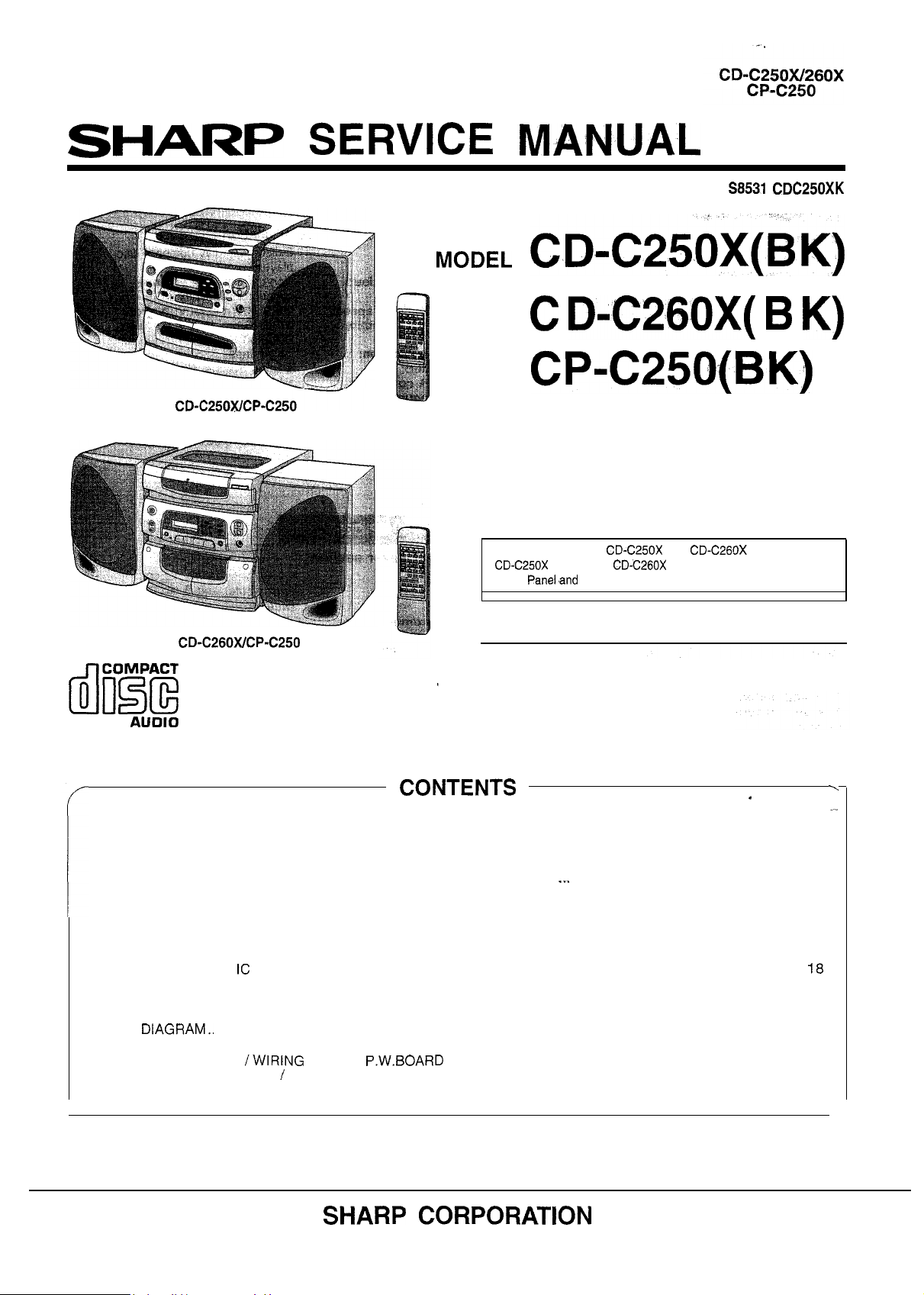
Illustration:
Illustration:
No.
l
Difference between
Front
l
In the interests of user-safety the set should be restored to its original
condition and only parts identical to those specified be used.
differs from
CD Cover but their functions are the same.
and
only in the design of cassette lid,
DIGITAL
SPECIFICATIONS..
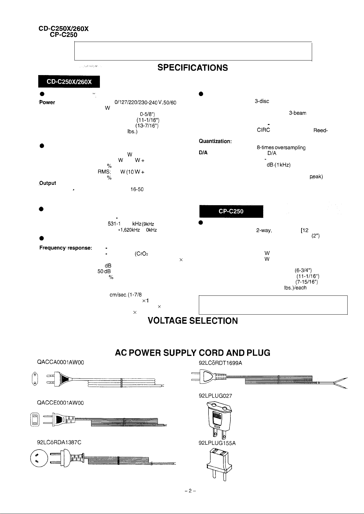
VOLTAGE SELECTION
AC POWER SUPPLY CORD AND PLUG
NAMES OF PARTS
OPERATION
DISASSEMBLY
REMOVING AND REINSTALLING THE MAIN PARTS
ADJUSTMENT .................................................................................................................................................................
TROUBLESHOOTING (CD SECTION) ............................................................................................................................
FUNCTION TABLE OF
LCD
SEGMENT.. ..............................................................................................................................................................
NOTES ON SCHEMATIC DIAGRAM ...............................................................................................................................
TYPES OF TRANSISTOR
BLOCK DIAGRAM..
WAVEFORMS OF CD CIRCUIT ......................................................................................................................................
SCHEMATIC DIAGRAM /WIRING SIDE OF
REPLACEMENT PARTS LIST / EXPLODED VIEW
............................................................................................................................................................
.................................................
..........................................................................................
MANUAL
......................................... .........................................................................................................................
......................................................................................................................................................
................................................................................................................................................
................................................................................................................................................
...........................................................................................................................................................
..........................................................................................................................
....................................................................................................
...............................................................
.....................................................................................................
.............................................................................................
Page
10
12
21
22
22
23
27
29
2
2
2
3
5
6
8
Page 2
FOR A COMPLETE DESCRIPTION OF THE OPERATION OF THIS UNIT, PLEASE REFER
TO THE OPERATION MANUAL.
General
source:
Power consumption:
Dimensions:
“Weight:
Amplifier section
Output power:
terminals:
11
AC
80
Width; 270 mm (1
Height; 280 mm (11-l/16”)
Depth: 340 mm
5.6
PMPO; 100
MPO; 36
(10
(10
Speakers; 8 ohms
Headphones;
(recommended; 32 ohms)
kg (12.3
(18 18 W)
T.H.D.)
20
T.H.D.)
(total)
10 W)
ohms
Hz
Compact disc player section
Type:
Signal readout:
Rotational speed:
Error correction:
Filter:
converter:
Frequency response:
Dynamic range:
Wow and flutter:
Tuner section
Frequency range:
FM; 88
AM; 531-l ,602
108 MHz
530
(1
span)
span)
Speaker section
Type:
Cassette deck section
Maximum input
power:
Rated input power:
Impedance:
Dimensions:
Weight:
Specifications for this model are subject to change without
prior notice.
Motor:
Signal/noise ratio:
Wow and flutter:
Bias and erasure
system:
Tape speed:
Heads:
50
14,000 Hz (Normal tape)
50
15,000 Hz
DC motor with electronic governor x 1
55
(TAPE 1, playback)
(TAPE 2, recording/playback)
0.15
(WRMS)
AC
4.76
TAPE-l: Playback x
TAPE-2: Record/playback x 1
Erase x 1
tape)
ips.)
The voltage selector is located on the AC voltage selector box. If
adjustment is necessary, use a screwdriver in order to slide the selector
to match to the correct voltage.
multi-play compact disc
player
Non-contact,
conductor laser pickup
200
500 rpm CLV, Approx.
(Cross Interleave
Solomon Code)
16 bit linear
l-bit
20
90
Unmeasurable
(less than 0.001% W.
3/4”) woofer and 5 cm
tweeter]
20
10
8
Width; 170 mm
Height; 280 mm (11-l/16”)
Depth; 201 mm
2.3 kg (5.1
20,000
bass-reflex
ohms
converter
Hz
semi-
digital filter
cm (4-
Page 3
Front
panel
1.
Disc Tray
CD Repeat Indicator:
6.
Disc Number Indicator
Extra Bass Indicator: X-BASS
CD Play Indicator:
11.
Record Indicator
12.
Preset Channel Indicator
13.
FM Stereo Indicator:
14. Function/Track Number/CD Counter/
Band/Frequency/Volume Indicator
15.
Memory Indicator
16.
Power Switch
17.
Record Start Button:
Stand-By Indicator
19.
Remote Control Sensor
Extra Bass Button: X-BASS
Disc Number Select Buttons
Function Selector Buttons
23.
Volume Up/Down Buttons:
24.
Tuning
25.
Reset Button
26.
Track Down/Review/Preset Down Button:
27.
Stop Button:
28.
Play/Repeat Button:
Track Up/Cue/Preset Up Button:
Equalizer Mode Button
Memory Button
32.
(TAPE 1) Cassette Compartment
(TAPE 2) Cassette Compartment
Buttons:
Socket
Illustration:
6171819
24
25
26
272829.30
33 34
2223
31
32
Page 4
n
Rear panel
AM Loop Aerial Socket
FM 75 ohms Aerial Terminal
Speaker Terminals
6.
AC
Voltage
n
Speaker section
Tweeter
8.
Woofer
TO.
Speaker Wire
Left speaker
Right speaker
q
Remote control
Remote Control Transmitter Window
CD control section
Disc Number Select Buttons
Track Down/Review Button:
n
Disc Skip Button
6.
Track Up/Cue Button:
Play/Repeat Button:
8.
Random Button
Clear Button
Memory Button
11.
Pause Button:
Tuner control section
II
I
Tape control section
(TAPE 1) Play Button:
1)
Stop Button:
15.
(TAPE 2) Stop Button:
16.
(TAPE 2) Rewind Button:
17.
(TAPE 2) Play Button:
18.
(TAPE 2) Fast Forward Button:
n
A
19.
Balance Control Buttons
Function Selector Buttons
Equalizer Mode Buttons
22. Volume Up/Down Buttons:
Extra Bass Button: X-BASS
24.
Power
Button
Page 5
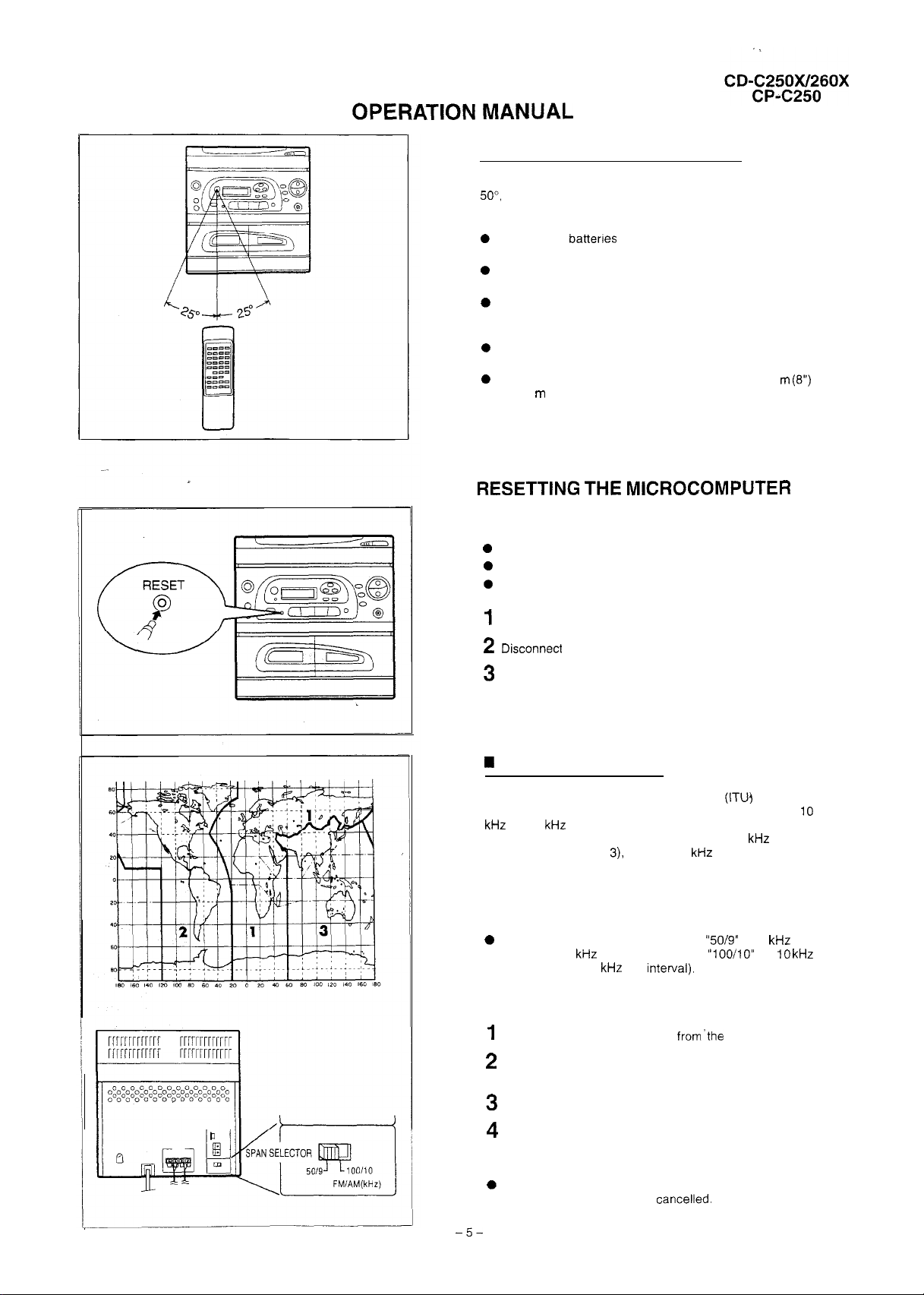
n
Proper use of the remote control
Aim the remote control at the remote control sensor within
with no obstacles, and operate as shawn.
Notes concerning use:
Replace the battenes if control distance decreases or
operation becomes erratic.
Periodically clean the transmitter window on the remote
control and the sensor on the main unit with a soft cloth.
Exposing the sensor on the main unit to strong light can
interfere with operation. Change the lighting or the direction of the unit.
Keep the remote control away from moisture, excessive
heat, shock, and vibrations.
The remote control’s usable range is between 0.2
and 6
(20’) away from the sensor.
MICROCOMPUTER
Reset the microcomputer by performing the following
procedure for the cases shown below:
To erase all of the stored memory contents, or
If the display does not function properly, or
The unit does not operate properly.
Set the POWER switch to STAND-BY.
the AC power lead from the AC socket.
Press the RESET button for at least 5 seconds
AM/FM interval (span)
The International Telecommunication Union
lished that member countries should maintain either a
or a 9
of any AM station. The illustration shows the 9
zones (regions 1 and
gion 2).
Before using the unit, set the SPAN SELECTOR switch (on
the rear panel) to AM tuning interval (span) of your area.
Set the SPAN SELECTOR switch to
interval (50
AM interval (100
interval between broadcasting frequencies
and the 10
FM interval), and
FM Interval).
To change the tuning zone:
Disconnect the AC power lead
has estab-
interval
interval zone (re-
for 9
for
AC socket
AM
Press the RESET button on the front panel for at least
3
seconds.
Set the SPAN SELECTOR switch as desired.
Reconnect the AC power lead into an AC socket.
Note:
When the SPAN SELECTOR switch is switched, the
memorised stations will be cancelled.
Page 6
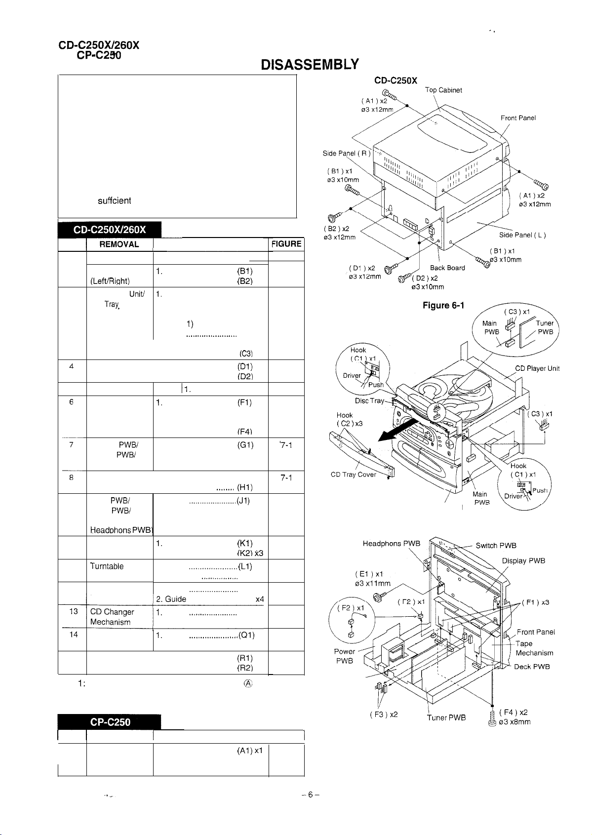
Caution on Disassembly
Follow the below-mentioned notes when disassembling the
unit and reassembling it, to keep it safe and ensure excellent
performance:
1. Take cassette tape and compact disc out of the unit.
2. Be sure to remove the power supply plug from the wall
outlet before starting to disassemble the unit.
3. Take off nylon bands or wire holders where they need be
removed when disassembling the unit. After servicing the
unit, be sure to rearrange the leads where they were
before disassembling.
4. Take
care on static electricity of integrated
circuits and other circuits when servicing.
Illustration:
STEP
12Top Cabinet
Side Panel
CD Player
3
CD
Cover
PROCEDURE
1
Screw......................
Screw.. ....................
2.
Screw.. .................... (82) x2
Turn on the power supply,
open the disc tray, take out
the disc tray, and close.
(Note
2. Hook
3.
Hook . (C2) x3
4.
Socket . . . . . . . . . . . . . . .
Back Board
5
Headphons PWB Screw . (El) xl
Front Panel
(Note 2)
Display
Switch
Sub PWB
1.
Screw......................
2.
Screw.. ....................
Flat Cable ...............
2. Socket ..................... (F2) xl
3.
Socket.. ...................
4.
Screw.. ....................
1.
Socket.. ...................
2.
Screw.. ....................
3. Screw.. .................... (G3) xl
Tape Mechanism 1. Open the cassette holder
2.
Screw
9
Main
Deck
Tuner PWB (with
1 Screw
2.
Screw (J2) xl
3. Socket . . . . . . . . . . . . . . . . . (J3) xl
10
CD Servo PWB
11
12
Disc Tray
Screw.. ....................
2. Socket .....................
1 Screw
2. Cover . . . .
1. Screw
(M2)
Screw
(Al) x4
x2
(Cl) x2
x2
x2
x2
x3
(F3)
x2
x2
xl
(G2) x9
(Hl)
x6
(Jl
x5
xl
it3
xl 7-4
(L2) xl
(Ml) x4
(Pl) x4
6-l
6-l
6-2
6-l
6-3
6-3
7-2
7-3
7-4
7-5
c2
Front Panel
Figure 6-2
CD
Mechanism
(Note 3)
15
Senser PWB
Note
if the power supply cannot be turned on,
Screw
1. Screw ......................
2. Socket .....................
by hand as shown in Figure 7-3 to open the disc tray.
Note 2: Withdraw upward straight the flat cable.
STEP
1
REMOVAL
Speaker
PROCEDURE
1.
Net
..........................
2. Front Panel .............
3. Screw.. .................... (A3) x6
xl
xl
turn the gear
FIGURE
(A2) xl
7-5
7-5
7-6
7-7
Main
PWB
PWB
Figure 6-3
Note 3: After removing the Flexible PWB for the optical pickup
from the connector wrap the conductive aluminum foil
around the front end of Flexible PWB so as to protect
the optical pickup from electrostatic damage.
Page 7
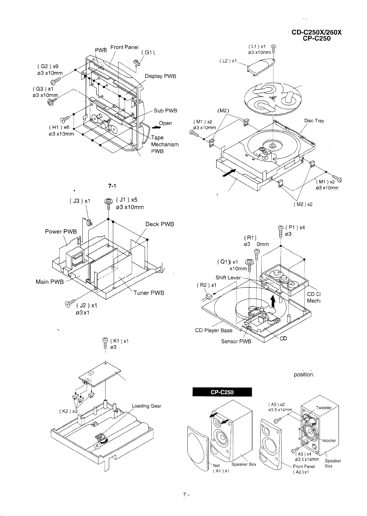
Switch
Figure
Tape Mechanism
xl
Turntable
x2
CD Player
Unit
Figure 7-4
Omm
Figure 7-2
)x1
xl Omm
CD Servo PWB
RI
xl
xl
xl
02.6
hanger
anism
. .
Mechanism
Care when installing the CD changer mechanism.
Install the CD changer mechanism on the CD player base after
the shift lever has been set in the highest
Figure 7-5
Figure 7-3
Figure 7-6
xl4mm
Figure 7-7
Page 8
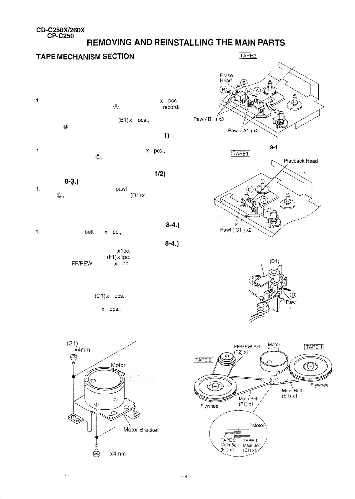
Perform steps 1, 2, 3, 4, 6 and 8 of the disassembly method to
remove the tape mechanism.
How to remove the record/playback and erase
heads (TAPE 2) (See Fig. 8-l.)
Carefully bend the record/playback head pawls (Al) x 2
in the direction of the arrow
playback head upwards.
2. Carefully bend the three pawls
direction
and remove the erase head upward.
and remove the
x 3
in the arrow
How to remove the playback head (TAPE
(See Fig. 8-2.)
Carefully bend the playback head pawls (Cl) x 2
direction of the arrow
upwards.
and remove the playback head
in the
How to remove the pinch roller (TAPE
(See Fig.
Carefully bend the pinch roller
arrow
Note:
When installing the pinch roller, pay attention to the spring
mounting method.
and remove the pinch roller
in the direction of the
x 1 upwards.
Bl
Record/Playback
Head
Figure
How to remove the belt (TAPE 1) (See Fig.
Remove the main belt (El)
1
from the motor side.
How to remove the belt (TAPE 2) (See Fig.
1. Remove the tape 1 main belt (El)
2. Remove the tape 2 main belt
3. Remove the
belt (F2) x 1
from the motor side.
x from the motor side.
How to remove the motor
(See Fig. 8-5.)
1. Remove the belt.
2. Remove the screws
bracket.
3. Remove the screws (G2) x 2
Note:
When mounting the motor, pay attention to the motor mounting
angle.
x2
02
2
to remove the motor
to remove the motor.
Figure 8-2
Pinch Roller
Figure 8-3
xl
(G2) x2
02
Figure 8-5
Figure 8-4
Page 9
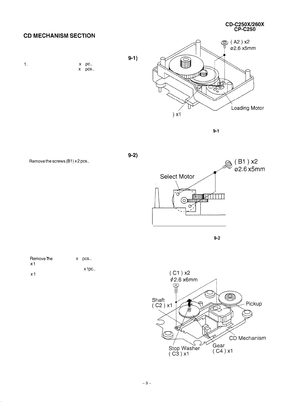
MECHANISM SECTION
Perform steps 1, 2, 3, 10, 11, 12, and 13 of the disassembly
method to remove the CD mechanism.
How to remove the loading motor (See Fig.
Remove the drive belt (Al) x 1
2. Remove the screws (A2) x 2
motor.
How to remove the select motor (See Fig.
1.
from the motor side.
to remove the loading
toremovetheselectmotor.
(Al )x1
Drive Belt
Figure
x5mm
How to remove the pickup (See Fig. 9-3)
1. Removethe screws (Cl)
pc.
2. Remove the stop washer (C3)
pc.
3. Remove the pickup.
Note:
After removing the Flexible PWB for the optical pickup from the
connector wrap the conductive aluminum foil around the front
end of Flexible PWB so as to protect the optical pickup from
electrostatic damage.
2
to remove the shaft (C2)
to remove the gear (C4)
Figure
Figure 9-3
Page 10
l
Driving Force Check
Torque Meter
Play:
TW-2412
l
Check
Torque Meter
Fast forward: TW-2231
Rewind: TW-2231
l
Tape Speed
Test Tape
Normal
MTT-111
speed
TAPE MECHANISM
Tape 1: Over 80
Tape 2: Over 80
Tape
30 to
60
Adjusting
Point
Volume in
motor.
Specified Value
Specified Value
1
cm
Tape 2
30to60
Specified Instrument
Value
3,000 i:
30 Hz
Connection
Speaker
terminal
(Load
resistance:
6 ohms)
Low-range frequency
High-renge frequency
l
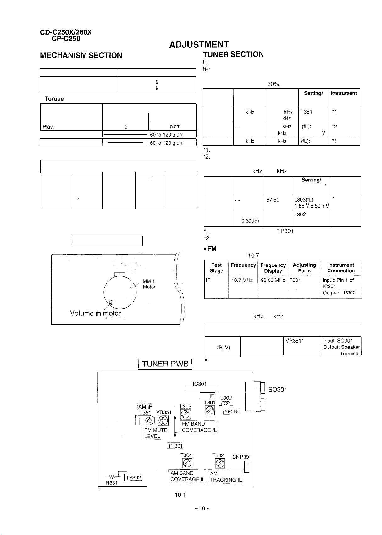
AM IF/RF
Signal generator: 400 Hz,
Test Stage
IF
Frequency
450
Band
Coverage
Tracking
Input: Antenna,
Input: Antenna,
l
FMRF
990
Output: TP302
Output: TP301
Signal generator: 1
Test Stage Frequency Frequency
Band
Coverage
RF
Input: Antenna,
Input: Antenna,
98.00 MHz 98.00 MHz
(1
Output:
Output: Speaker terminal
AM modulated
Frequency
Display
1,602
1,620
531
530
990
22.5
Display
MHz
Adjusting Connection
Parts
or
or
T304
1.1 IO.1
T302
dev., FM modulated
instrument
Adjusting
Connection
Point
l
2
TUNER
Signal generator:
l
FM Mute Level
Signal generator: 1
Frequency
MHz, FM sweep generator
40
Frequency
Display Parts
98.00 MHz
98.00 MHz
(25
Adjust so that an output signal appears.
FM
dev., FM modulated
Adjusting
FM ANTENNA
TERMINAL
Instrument
Connection
Figure 10-l ADJUSTMENT POINTS
AM
ANTENNA
TERMINAL
Page 11
l
Setting the test mode
Any one of 4 test modes can be set by pressing several keys as follows
TEST
CD operation test
l
TEST 4 mode
Function
<CD>
CD test mode
Setting of TEST 4 mode
of CD TST mode (All LCD lights)
IL is not performed.
pickup can be moved by using the
<MEMORY>
When the tracking servo is
turned on, PLAY is started at
<STOP>
The pickup returns to the
ordinary stop position.
once.
TOC. IL is performed, and the ordinary PLAY is performed.
If the following key is pressed during PLAY, it is possible to
specify directly any Track No.
Note:
Number
<Disc Number
Number
key: Track 3
key: Track 8
key: Track 15
Only in STOP state it is possible to slide the pickup with the
VOL. --- Last memory
--- FLAT
X-BASS --- OFF
Canceling method
POWER OFF
SECTION
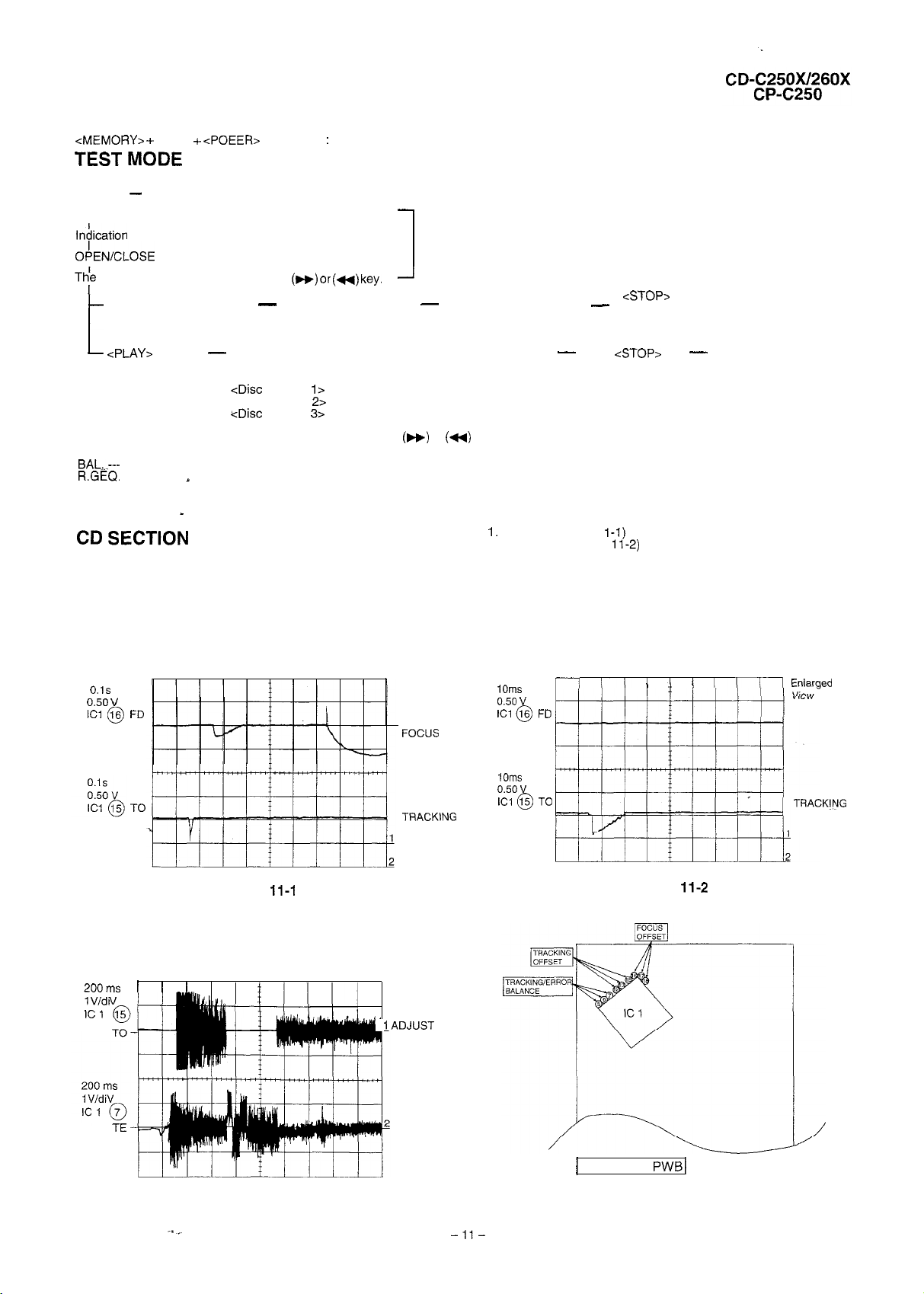
Since this CD system incorporates the following automatic adjustment
function, when the pickup is replaced, it is not necessary to readjust it.
l
Automatic adjustment item
<MEMORY>
When the tracking servo is
turned off, PLAY is started
at once.
or
key.
Focus offset (Fig. 1
2. Tracking offset (Fig.
3. E/F balance (tracking error balance) (Fig. 11-3)
4. RF level AGC function (HF level: constant)
5. RF level automatic follow-up of the tracking gain
This automatic adjustment is performed each time a disc is changed.
Therefore, each disc is played back using the optimal settings.
The pickup returns to the
ordinary stop position.
Press
key.
Stop
OFF-SET
ADJUST
OFF-SET
OFF-SET
ADJUST
ADJUST
Figure 11-l
Figure
TRACKING/
ERROR
BARANCE
CD SERVO
Figure 1 l-3
Figure 11-4 CHECKING POINTS
Page 12
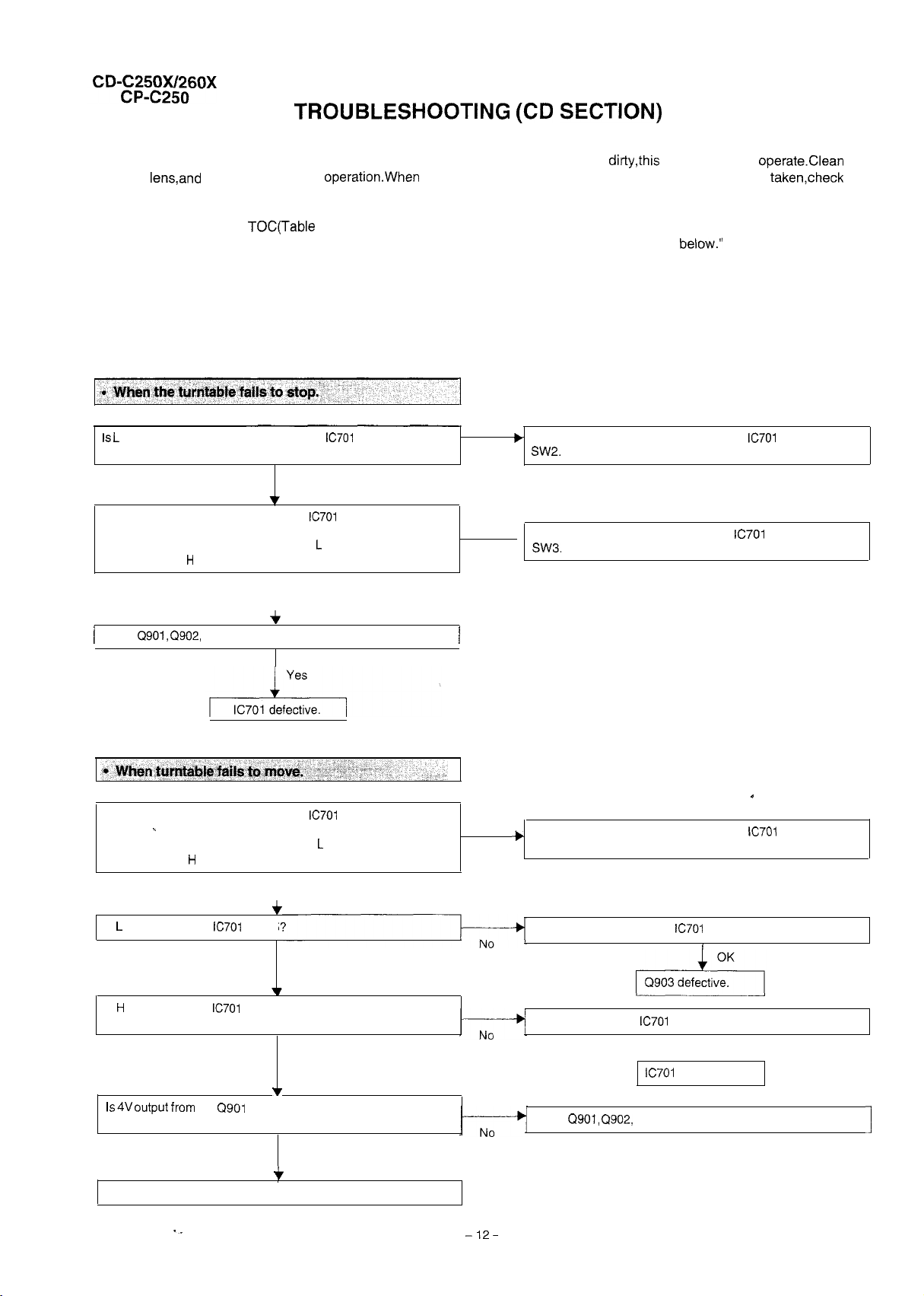
When the CD does not function
When the CD section does not operate When the objective lens of the optical pickup is
objective
following items.
Remove the cabinet and follow the troubleshooting instructions.
“Track skipping and/or no TOC(Table Of Contents) may be caused by build up of dust other foreign matter on the laser pickup lens.
Before attempting any adjustment make certain that the lens is clean. If not, clean it as mentioned
Turn the power off.
Gently clean the lens with a lens cleaning tissue and a small amount of isopropyl alcohol.
Do not touch the lens with the bare hand.
pulse (approx. 300 ms) input into the
turntable is rotating?
check the playback
this section does not operate even after the above step is takencheck the
pin 26 when the
Check the SW2 and the wiring from the
No
section may not
the
pin 26 to the
,
Is there following voltage input on the
state?
When the CD mechanism is moved up:
In other states:
Check
Is there following voltage input on the
state?
When the CD mechanism is moved up:
In other states:
and Q904 and the periphery.
Yes
Yes
Yes
pin 9 in the specific
pin 9 in the specific
, Check the SW3 and the wiring from the
No
Check the SW3 and the wiring from the
No
sw3.
pin 9 to the
pin 9 to the
IS output from the
Is
output from the
switch is pressed?
output
above?
Check turntable motor (Ml) and turntable mechanism.
the
pin 25
I
Yes
pin 19 during SEC when the disc skip
Yes
emitter during operation stated
Yes
Check the wiring from the
Check the wiring of
Check
pin 19 and Q904 pin 2.
defective.
Q904 and the periphery.
pin 25 to the Q903 base.
OK
Page 13
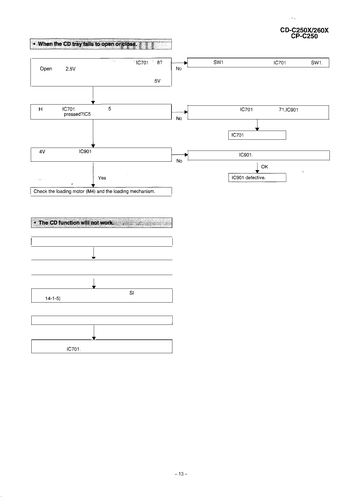
Is there following voltage input in specific state
of
Close state: OV
Intermediate state between open state and close state:
Yes
Is
output to
CLOSE key is
pin 70 or 71 for
is defective. Replace it.
seconds when the OPEN/
pin
Check the
and the wiring from the
Check the wiring of the
and 9.
pins 70 and
OK
pin 8 to the
pins 1
Yes
Is 4V output between
pins 3 and 7 during operation stated
above?
The CD operating keys don’t work.
Yes
Check the CD, DPS microcomputer, power supply, 4.19 MHz and
16.93 MHz clock, and reset terminal.
Yes
Check the waveform of SCK, SO (DATA) and
(COMM).
(Fig.
defective.
Check the periphery of
I
Yes
See if the pick-up is in the pick-up in SW4 position.
Yes
If the items mentioned above are OK, check the main
microcomputer
Page 14
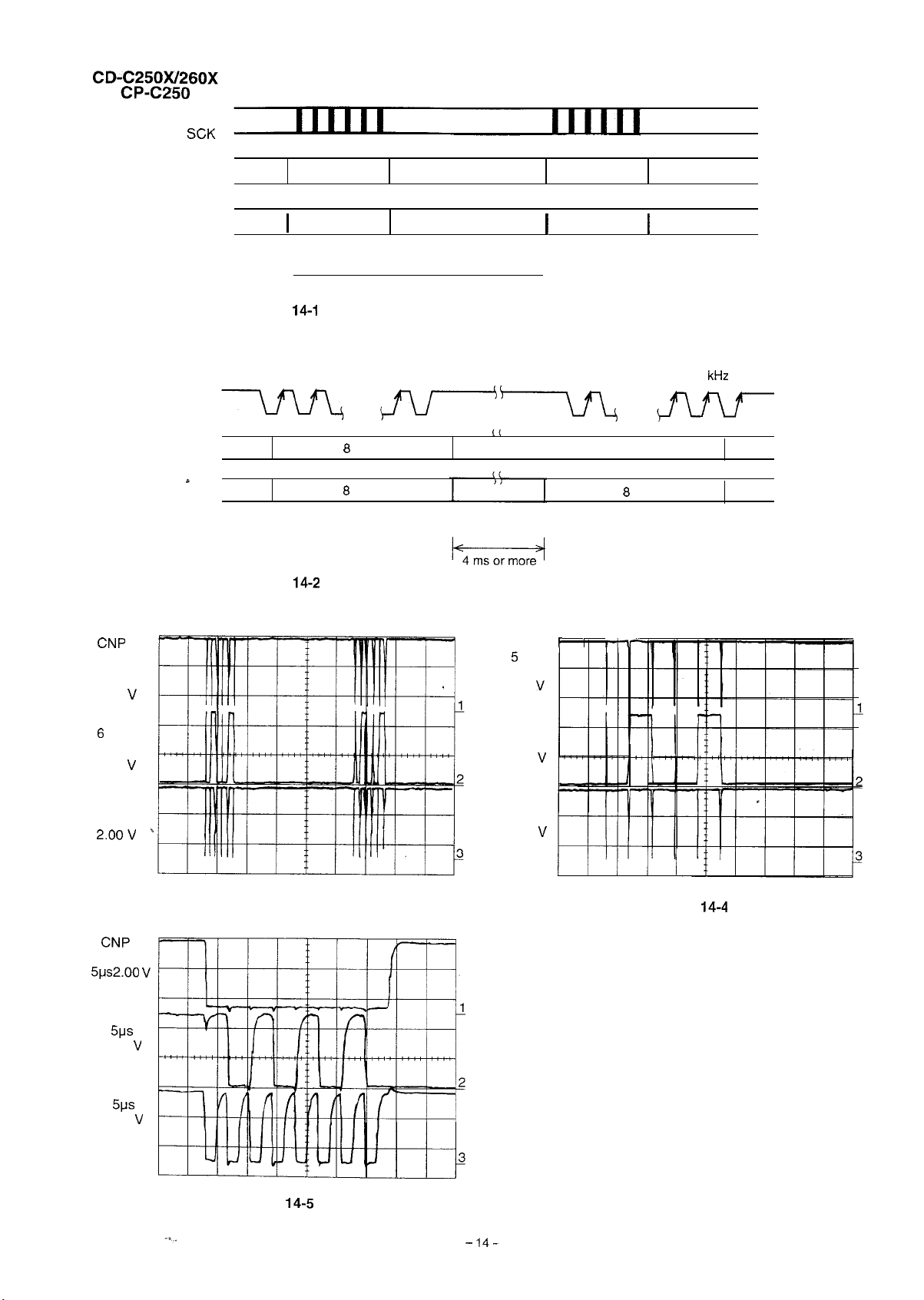
COMM
6 BYTE
6 BYTE
7
5 Pin
20ms
2.00
COMM
Pin
20ms
2.00
DATA
7 Pin
20ms
SCK
DATA
6 BYTE
6 BYTE
100 ms interval
Figure
CD microcomputer -- Main microcomputer data transmission
CK: 262
or less
SCK
COMM
DATA
BIT
BIT
I
8 BIT
BIT
DATA and COMM are read
at rise of SCK.
LSB FIRST
Figure
CD microcomputer --
Main microcomputer data transmission
CNP 7
Pin
5ms
2.00
COM
6 Pin
5 ms
2.00
DATA
7 Pin
5 ms
2.00
SCK
5 Pin
COM
6 Pin
2.00
DATA
7 Pin
2.00
SCK
Figure 14-3
Figure
7
Figure
14-
Page 15
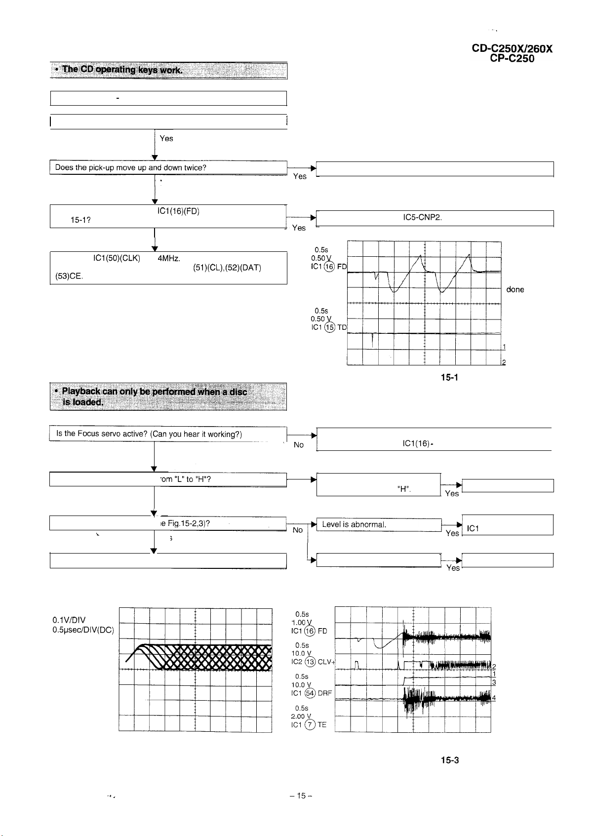
Check the Focus
HF svstem.
Playback can be performed without a disc.
Yes
No
Focus search OK
Does the output waveform of ICi(lG)(FD) match that shown in
Fig.
No
Check the
Check the microcomputer data on pins
line,
Yes
Does the DRF signal change fr
Yes
and
No
Check the area around IC5CNP2.
Figure 15-l
Check the laser diode driver.
Check the area around
If the disc is not turning, the DRF
should not change to
(21) (focus servo circuit).
Check the spin system.
Focus search
is performed
two times
when play
operation is
disc.
Is HF waveform normal (see th
Check the tracking system.
HF
(When playing
back the disc)
Figure 15-2
Yes
Check the periphery-of
Waveform is unstable. Check the spin system.
Figure
Waveform in
case of normal
play-back
Page 16
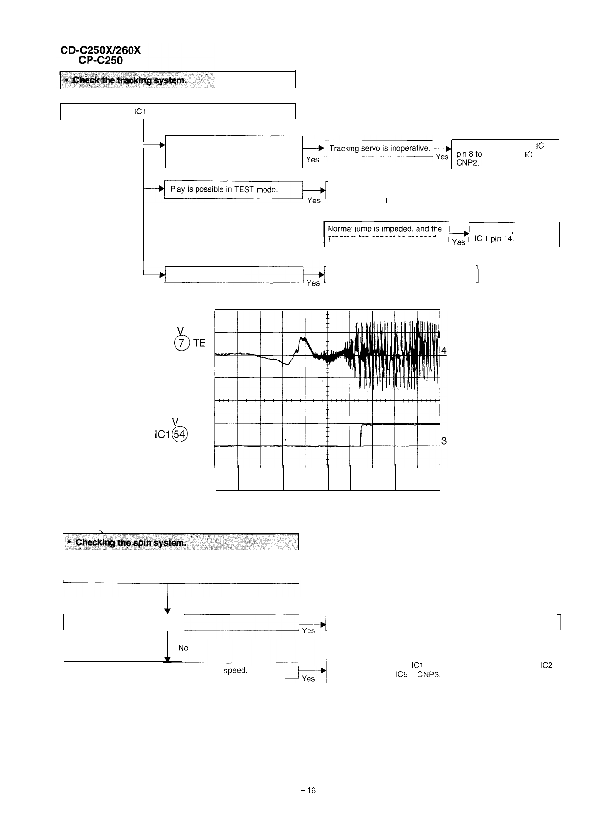
Check waveform of ICl pin 7 (TE).
The waveform shown in Fig.16
appears, and no-disc state apperas
soon.
Data cannot be read.
5ms
1.00
ICI
5 ms
5.0
DRF
Although IL is possible, play is impossible.
Yes
program top cannot
I
Check the VCO-PLL system.
be reached.
Check the periphery of
pin 15, and
Check the periphery of
1
5 to
Play operation is performed without disc.
Yes
The turntable rotates a little.
The turntable fails to rotate or rotates at
high speed.
Figure 16
The spin driver circuit is normal.
Check the periphery of ICl pins 23 to 27, pin 39, and pin 40,
pin 13 and pin 14,
to
Page 17
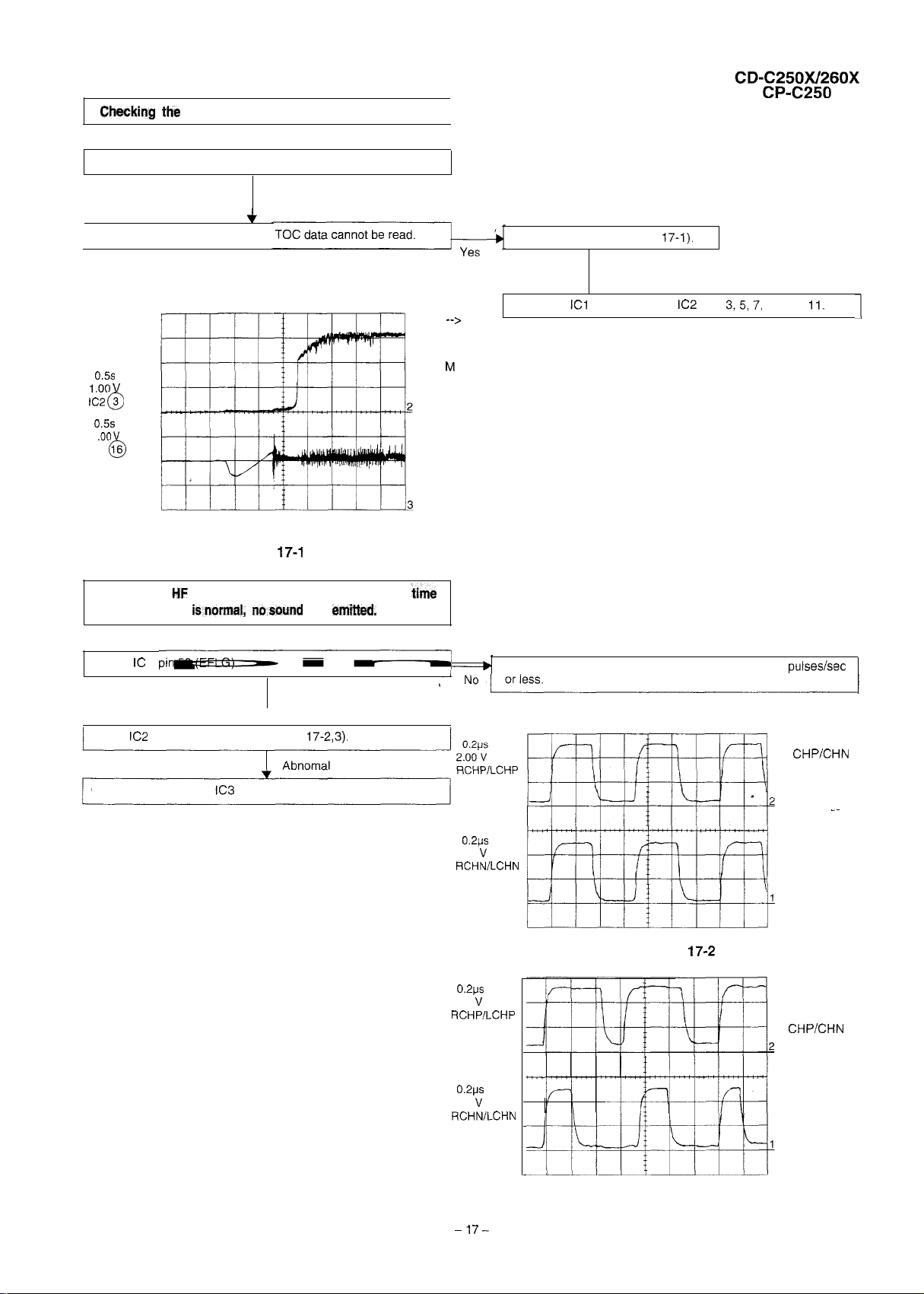
l
Play operation is performed when disc exits.
VCO-PLL system
Yes
1
Although HF waveform is normal,
PDO
1
ICI
FD
Figure 17-l
l
Although MF waveform is norm& ‘and the
indication
Check
2
is
Stop
Play
As VCO freque-
ncy is locked at
4.32
Hz,
voltage of PDO
rises and stabili-
zes.
Check PDO waveform (Fig.
Error
Check the
Usually, the number of pulses of flawless disc is 100 pulsesisec
pins 43 and 44,
pins
10, and
Check
Check the periphery of
pins 48, 49, 52, and 53 (Fig.
(OPAMP).
Yes
2.00
2.00
2.00
In STOP state
clocks are the
same. and output is not
given.
Figure
Due to difference in waveform of
(duty ratio)
in PLAY
mode output
is given.
Figure 17-3
Page 18

RHiX0039AWZZ (IX0039AW):CD Control Microcomputer
Pin No. Port Name
PGO
2
3
4
5
6 AV-
7
9
10
11
12
13
14
15
17 PCO”
20
21 PDO
22
24
PG2 CQCK
PG3
vss
VDD
RES
TEST
SCK(PF2)
PC2
PC3 LASER
PD3
PEO
Terminal Name input/Output
SQOUT
COIN
RWC
COMM Input
DATA
SCK
PU-IN SW
DRF
WRQ
RES
Input
output
output
output
Input
Input
output
output Servo AMP slide feed output
output
output
Input
Input
input
Input
output
Function
Servo/signal control data input
Servo AMP, servo/signal control command output
Servo AMP, servo/signal control clock output
Servo AMP, servo/signal control
Connect to AD converter reference voltage input terminal GND.
Connect to AD converter reference voltage input terminal GND.
Connect to VSS terminal
OSC
Power terminal
Reset
Test
Serial data input from main microcomputer
Serial data output from main microcomputer
Servo AMP. slide return output
Input/output common port C-2
Pickup internal periphery position detection input; innermost periphery
Servo AMP. RF detection input
Input/output common port D-2
Servo/signal control request
Input/output common port E-l
Servo/signal
Input/output common port A-l
or ceramic oscillator
when laser is on
common
control reset output
E-O
control
In this unit, the terminal with asterisk mark
is (open) terminal which is not connected to the outside.
I
I I
l-r
.
Figure 18 BLOCK DIAGRAM OF
Page 19

(LC75395E) or VHiLC75394E-i(LC75394):Audio
C2
SHIFTREGISTER
Figure 19 BLOCK DIAGRAM OF
Page 20

AWZZ
AW):System control Microcomputer
Pin No.
11
15.16
17-18
19
20
25
26
27 RESET
Port Name
P57
P56
P47
P46
Terminal Name
ADT
TOUT
-CNTR2 In/Output
SRDY
SCLK
0
RESET
Input
In/Output
In/Output
In/Output
In/Output
In/Output
In/Output
In/Output
In/Output
Input
Function
Supply voltage of 0-VL2 to LCD
CMOS input level CMOS 3 state output. (8 bit I/O port.)
CMOS input level CMOS 3 state output. (8 bit I/O port.)
CMOS input level CMOS 3 state output.
CMOS input level CMOS 3 state output. (8 bit
CMOS inout level CMOS 3 state outout.
CMOS input level CMOS 3 state output. (8 bit
CMOS input level CMOS 3 state output. (7 bit I/O port.)
CMOS input level CMOS 3 state output. (7 bit
CMOS input level CMOS 3 state output. (7 bit I/O port.)
CMOS input level CMOS 3 state output. (7 bit I/O port.)
CMOS input level CMOS 3 state output. (7 bit
CMOS input level (1 bit input port.)
The orocessor is reset. if held at
bit
bit
for more than
port.)
port.)
port.)
port.)
port.)
port.)
57-60 (60’)
61-72
73
74 VREF VREF
75 AVSS
76-79
80 VL3
In this unit, the terminal with asterisk mark
I vcc I vcc
AVSS
CMOS inout level.
output LCD segment output pin.
Power terminal
input
In/Output
output
Input
is (open) terminal which is not connected to the outside.
Input pin for the A-D converter reference voltage.
GND input for A-D converter. Connect to VSS
LCD common output pin.
Supply voltage of VL3 to LCD.
bit inout
I
Page 21

COMO
COM2
COM3
s22
Page 22

. Resistor:
To differentiate the
are used: the symbol
of resistors, the
symbol
means 1000 ohm and the symbol
means 1000 kohm and the resistor without any symbol is an
ohm resistor. The resistor designated “Fusible” is a fuse type
resistor.
l
Capacitor:
To indicate the unit of capacitor, a symbol
symbol
means pica-farad and the unit of the capacitor
is used: this
without such a symbol is microfarad. As to electrolytic capacitor, the expression “capacitance/withstand voltage” is used.
(CH), (TH),
(UJ): Temperature compensation
(ML): Mylar type
(P.P.): Polypropylene type
l
Schematic diagram and Wiring Side of
for this
model are subject to change for improvement without prior
notice.
. The indicated voltage in each section is the one measured by
Digital Multimeter between such a section and the chassis
with no signal given.
In the tuner section,
indicates AM
indicates FM stereo
2. In the main section, a tape is being played back.
3. In the deck section, a tape is being played back.
indicates the record state.
4. In the power section, a tape is being played back.
5. In the CD section, the CD is stopped.
l
Parts marked with
are important for
maintaining the safety of the set. Be sure to replace these
parts with specified ones for maintaining the safety and
performance of the set.
FOOL PROOF
SWM4
SWM5
I
I
GR
F.
CAM
A. S.
OFF
OFF
OFF
C
SR
SE
A
ES
KRA102
KTC3199 GR
Figure 22 TYPES OF TRANSISTOR AND LED
Page 23

PICKUP UNIT
I
I
I
I
I
XIN II
FOCUS COtL
TRACKING COIL
SLIDE
MOTOR
Ml
SPIN
MOTOR
I
I
CONTR
LASER
PICKUP IN
RESET
RESET
PU-IN SW
Figure 23 BLOCK
-23-
Page 24

XOUT
CONTROL
TO MAIN MICON
OUT
CNP7
GND
COM
DATA
SCK
B6)
LASER
RESET
8 9
CONTROL
x2
XL2
DIAGRAM
SC
SCK
VDD
REGULATOR
-24-
Page 25

SO301
FM
FRONT END
PLL CONTROLLER
Figure 25 BLOCK
Page 26

I
SYSTEM CONTROL
VOLTAGE
REGULATOR
VOLTAGE
REGULATOR
VOLTAGE
REGULATOR
AMP
LOCK DIAGRAM (2/2)
Page 27

5ms
STOP-PLAY
FOCUS- SERCH
.
CUE
5.0
HF
5.0
HFL
5.0
TES
DRF
CUE
0.50
JP
50ms
.
.
0.50
JP
TE
HF
5.0
5.0
TES
REVIEW
.
.- .
-_-----------
27
.
.
.
0.50
JP
REVIEW
Page 28

.
10.0
PLAY
TCD-712
5s
SLD
0.50
JP
.
TE
I
I
PLAY
NORMAL DISC
20ms
SLD
50ms
1.00
50ms
2.00
PLAY
TCD-712 (140mm)
Page 29

6-A
TAPE MOTOR
CNSM I
MECHANISM
RECORD/PLAYBACK
HEAD
ERASE HEAD
l
The numbers
1
to
are waveform numbers shown in page
2 3 4
5
I
6
Figure 29 WIRING
-29-
_.__
Page 30

2-A
SUB
(CD SERVO
I-B
PLAYBACK HEAD
7
SIDE OF P.W.BOARD
NT
m-i-
-H-
8
CD
9
10
11
12 I
30
Page 31

l
The numbers
1
to
are waveform numbers shown in page 27, 28.
I
.
2
I
l
NOTES ON SCHEMATIC DIAGRAM can be found on page 22.
3
I
4
I
5
I
Figure 31 SCHEMATIC
Page 32

I I
Page 33

G-A
7-G
G-A
4-A
A
MAIN PWB-AI
L-CH
SPEAKER TERMINAL
1
2
3
-33-
4
5
6
Figure 33 WIRING SIDE
Page 34

HEADPHONES
0
CNS4
I
SIDE OF
7 8 9
POWER PWB-A2
10
AC POWER SUPPLY CORD
AC
11
12 I
Page 35

I?-
l
NOTES ON SCHEMATIC DIAGRAM can be found on page 22.
. .
Figure 35 SCHEMATIC
-35-
Page 36

FM SIGNAL
SIGNAL
CD
AMP
--------
POWER
7
DIAGRAM
-------
8
9
10
11
12
I
Page 37

TAPE MECHANISM
TAPE DECK
PLAYBACK SIGNAL
RECORD
,
GNA
. NOTES ON SCHEMATIC DIAGRAM can be found on page 22.
2
.
3
-37-
4
5
6
Figure 37
I
Page 38

ACK AND
--- ___ __ J
AMP.
I I
DIAGRAM
-38-
Page 39

1
SYSTEM CONTROL
MICROCOMPUTER
l
NOTES ON SCHEMATIC DIAGRAM can be found on page 22.
I
I
3
I
4
I
I
Figure 39 SCHEMATIC
.
---
Page 40

DISPLAY PWB-A3
I
7 8 9 10
DIAGRAM
11
12
Page 41

2
3
4
6
9
I.
4.
I.
4.
4. iv
4.
4.
75
I
I
1 2 3
FM SIGNAL
(FM FRONT
END,
AM SIGNAL
10.
CF
1
I
,
I
0.033
OTHER
FM
1OOK
7K
,
. NOTES ON SCHEMATIC DIAGRAM can be found on page 22.
1
2
3
4
6
Figure
41
Page 42

PWB-D
I
SWITCHING
9
I
,
1K
1K
l FI
7 a 9
DIAGRAM
. .
10
11
12
I
Page 43

“HOW TO ORDER REPLACEMENT PARTS”
To have your order filled promptly and correctly, please furnish the following information.
1. MODEL NUMBER
3. PART NO.
SPARE PARTS-DELIVERY SECTION
NOTE:
Parts marked with
for maintaining the safety and performance of the set.
PART NO.
are Important for maintaining the safety of the set. Be sure to replace these parts with specified ones
DESCRIPTION
INTEGRATED CIRCUITS
Servo
Servo/Signal Control,
Ope
CD Control Microcomputer,
Focus/Tracking/Spin/
Slide
Playback and Record/
Playback
FM Front
PLL
FM IF
AM IF,LA1832
Audio Processor,
System Control
(Serial No.50600001
-507
System Control
(Serial No.
Power
Loading Motor Driver,
Only)
2. REF. NO.
4. DESCRIPTION
CODE REF.NO.
AV
BB
AC
AS
AS
AM
Q903
AG
AP
AR
AX
AZ
AZ
AM
AH
PART NO.
DESCRIPTION
(Serial No.50600001
-507X Only)
(Serial No.50600001
-507X
(Serial No.50600001
-507X Only)
DIODES
GR
ES
ES
ES
M
M
GR
M
GR
M
M
M
CODE
AB
AB
AB
AB
AD
AC
AD
AC
AC
AC
AD
AE
AE
AB
AC
AE
AB
AC
AD
AC
AC
AC
Q128
4353,354
TRANSISTORS
GR AB
M AC
SE AD
GR
GR
M AC
A AE
M AC
GR
M
M
C
SR
GR
M
GR
M
GR
AB
AB
AB
AB
AC
AC
AC
AD
AC
AC
AB
AB
AC
AB
AC
AB
D805
LED755
(Serial No.50600001
-507X
XXX Only)
AA
AA
AA
AA
AA
AA
AA
AA
AA
AA
AA
AA
AA
AG
AA
AA
AA
AB
AA
AD
AD
Page 44

\A
\A
\A
\A
\A
\A
\A
\A
\A
\A
\A
\A
\A
\A
\A
\A
\A
ZD351
ZD922
ZD923
PART NO.
VHCKV13
VHEMTZJ 5R6B- 1
OA2-F
DESCRIPTION
Variable Capacitance,
Variable Capacitance,
CODE
AS
AE
AD
AC
AC
AC
AC
AA
FILTERS
FM Band Pass Filter
FM IF
FM Detector
AD
AD
AH
TRANSFORMERS
T302
T304
FM IF
AM Antenna
AM Oscillation
AM IF
Power
AD
AD
AC
AF
BC
COILS
L302
L353
1901,902
FM RF
FM Oscillation
100
2.2
AC
AB
AB
AA
A
AB
AB
AB
AB
VARIABLE RESISTOR
VR351
kohm
[FM Mute Level]
AB
VIBRATORS
x351
X352
XL2
XL701
Crystal,456
MHz
MHz
MHz
MHz
AD
AK
AG
AD
AD
CAPACITORS
There are two types of capacitors available and they can be identified from
other by reading their Part Numbers.
Ceramic type capacitor;
A symbol “C” or
. .
Semiconductor type capacitor:
A symbol “T” is given at the 3rd digit of its Part Number like
The capacitance error of each capacitor is indicated by the symbol given at
13th digit of the Part Number as
(Tubular type ceramic capacitor is identified by the symbol
part NO.
(Tubular type ceramic capacitor is identified by the symbol MF(MN) of the par
NO.
Unless
"C"
is given at the 3rd digit of its Part Number like
“D” (t-O.5
this TV(TQ/CY) does not mean the lead wire.
this MF(MN) does not mean the lead wire.)
specified, electrolytic capacitors are
“Z”
“M”
of
type.
(o
Cl6
Cl8
c31
C32
c33
c34
c37
C38
c39
c43
C48
c49
c73
C81
Cl27
Cl46
PART NO.
DESCRIPTION
47
0.001 pF,5OV
0.033
0.068
0.047 ,uF,16v
180
0.1
330
0.1 ,uF,16V
0.01
0.0047
0.001 pF,5OV
0.47
1
47
0.0033
2.2
0.0027 ,uF,16V
27
0.001 pF,5OV
0.1
100
0.01
1
0.33
100
100
4.7
0.01
1
0.1
100
100
10
330
100
0.01
220
100
4.7
Electrolytic
180
0.001
0.047
22
330
47
560
1
0.01
0.022
3.3
470
0.001
22
0.056 ,uF,16V
0.0033
0.022 ,uF,25V
22
220
Al
Al
A,
Al
Al
A!
A/
AI
Al
A/
A/
A/
A/
A/
Al
A/
AI
AE
AE
AE
AC
AE
AE
AE
AE
AC
A/
AE
AE
AE
AE
AE
AE
AE
AE
AE
Cl
AA
Cl48
0.082
AE
Page 45

Cl56
C316
c331
C332
c334
c335
C336
C352
c355
C356
c357
c359
C362
C363
C364
C365
C366
c375
C382
C383
C384
C386
c392
c393
c394
c395
C396
C398
c399
PART NO.
DESCRIPTION
33
0.0039 ,uF,lOOV,
Polypropylene
0.027
F,SOV,Mylar
47
100
18 pF
0.01 /1F,16V
4.7 pF,5OV
15 pF (CH),SOV
33
0.0047 /~F,16v
12 pF (UJ),5OV
0.022
10
100
8.2 pF (UJ),5OV
22 pF
0.022 ,uF,25V
8.2 pF
18
18 pF
470
0.022
10
22
0.001
2.2
,uF,SOV,Electrolytic
3.3
22
0.001 fiF,5OV
1
0.018
3.3
12 pF
15 pF (CH),SOV
0.022
0.001
0.01
330
CODE
AB
AB
A0
AB
AA
AA
AA
AA
AA
AA
AA
AA
AA
AA
AA
AA
AA
AA
AA
AA
AA
AA
AA
AA
AA
AA
AA
AA
A0
AA
AA
AA
AB
AA
AA
AB
AA
AB
AA
AA
AB
AA
AA
AA
AA
AA
AA
AA
c443
c444
c735
C736
c737
c739
C756
ca21
C822
C823
C824
c921
c922
c927
CM2
PART NO.
DESCRIPTION
0.22
0.01 ,uF,25V
0.0022
0.0039
22
100
22
2.2 gF,EiOV,Electrolytic
10
220
0.01
47
0.01
3.3
0.01
0.022 ,uF,25V
220
56
22
(Serial No.50600001
-507
Only)
0.0027
1 ,uF,SOV,Electrolytic
100
1000
0.1
220
4.7
10
2200
0.22
47
47
47
0.01
47
3300
220
47
3.3
CODE
AA
AA
AB
AA
AA
AB
AA
AB
AB
AB
AA
AB
AB
AA
AA
AA
AA
AB
AB
AA
AA
AB
AA
AA
AA
AA
AB
AA
AB
AB
AD
AA
AB
AB
AB
AA
AH
AB
AB
AA
AB
AA
AB
AA
AB
AG
AB
AB
AB
AA
47
0.001
1
47
100
100
0.15
47
100
0.47
0.022 p F,SOV,Mylar
1
AB
AA
(Unless otherwise specified, resistors are
carbon film resistor
AA
AB
part NO.
AB
AA
AA
AB
AA
AA
AB
AA
RESISTORS
is identified the symbol
this TV(TQ/CY)
this MF(MN) does not mean lead
0
1
100
15
2.2
6.8
not
identified the symbol MF(MN) of the
Ivory
type.) (Tubular type
of the part NO.
AA
AA
AA
AA
AA
AA
-3-
-
-_
--
Page 46

R16
R20
R21
R22
R23
R24
R32
R35
R38
R49
R50
R51
R52
R53
R55
R56
R57
R60
R77
R78
R83
R87
R88
R116
R127
R128
R133
R134
PART NO.
100
12
27
82
3.3
15
33
10
47
1.5
82
82
39
56
6.8
1.2
10
1.2
220
1
56
5.6
470
47
33
22
100
4.7
1.5
15
1
10
5.1
27
680
10
100
10
6.8
10
470
22
1
470
560
1
3.3
6.8
10
1
56
100
3.9
5.6
8.2
8.2
33
22
68
3.3
6.8
560
DESCRIPTION
CODE
AA
AA
AA
AA
AA
AA
AA
AA
AA
AA
AA
AA
AA
AA
AA
AA
AA
AA
AA
AA
AA
AA
AA
AA
AA
AA
AA
AA
AA
AA
AA
AA
AA
AA
AA
AA
AA
AA
AA
AA
AA
AA
AA
AA
AA
AA
AA
AA
AA
AA
AA
AA
AA
AA
AA
AA
AA
AA
AA
AA
AA
AA
AA
AA
AA
AA
AA
AA
AA
AA
R143
R147
R148
R153
R154
R159
R178
R179
R301
R302
R303
R309
R312
R316
R317
R319
R320
R323
R324
R330
R331
R351
R352
R353
R354
R356
R358
R360
R367
R368
R376
R377
R379
R380
R381
R382
R383
R384
PART NO.
100
10
5.6
10
10
10
10
100
150
10
10
27
470
10
330
270
4.7
10
4.7
10
47
100
12
1
1
1
10
10
220
33
22
100
10
47
47
680
4.7
820
100
4.7
68
100
3.9
56
5.6
2.7
270
3.3
3.3
8.2
1.8
4.7
3.3
3.3
10
1
33
1
1
1
2.2
1.5
150
5.6
12
10
DESCRIPTION
CODE
AA
AA
AA
AA
AA
AA
AA
AA
AA
AA
AA
AA
AA
AA
AA
AA
AA
AA
AA
AA
AA
AA
.
AA
AA
AA
AA
AA
AA
AA
AA
AA
AA
AA
AA
AA
AA
AA
AA
AA
AA
AA
AA
AA
AA
AA
AA
AA
AA
AA
AA
AA
AA
AA
AA
AA
AA
AA
AA
AA
AA
AA
AA
AA
AA
AA
AA
AA
AA
AA
AA
Page 47

R386
R393
R395
R423
R424
R460
R475
R702
R703
R704
R706
R707
R709
R710
R720
R727
R731
R732
R735
R736
R737
R740
R741
R742
R743
R744
R748
R752
R754
PART NO.
DESCRIPTION
47
390
5.6
5.6
1
3.9
1
8.2
22
2.7
10
15
4.7
47
6.8
22
4.7
15
1.5
1.8
2.7
3.9
6.8
1.5
1.8
2.7
3.9
6.8
12
1.5
1.8
2.7
3.9
6.8
12
39
10
100
10
3.3
82
1
3.3
100
1
10
100
470
10
2.2
150
12
150
39
(Serial No.50600001
-507X Only)
1
(Serial No.50600001
-507X Only)
150
100
(Serial No.50600001
-507X
X
150
Only)
CODE
AA
AA
AA
AA
AA
AA
AA
AA
AA
AA
AA
AA
AA
AA
AA
AA
AA
AA
AA
AA
AA
AA
AA
AA
AA
AA
AA
AA
AA
AA
AA
AA
AA
AA
AA
AA
AA
AA
AA
AA
AA
AA
A
AA
AA
AA
AA
AA
AA
AA
AA
AA
AA
AA
AA
AA
AA
AA
AA
AA
AA
AA
AA
AA
R757
R769
R779
R781
R902
R904
R905
R917
R922
R923
R924
R927
R929
R930
R931
R932
R933
R940
RM2
RM3
RM4
RM5
RM7
CNP2
CNP3
CNP4
CNP7
CNP17
PART NO.
680
1
1
1
1
1
1
10
820
1
3.9
15
1
120
4.7
270
330
56
6.8
10
10
2.2
1
22
1
220
10
1
10
680
100
22
33
47
1
1
560
47
33
560
10
3.9
1
2.2
10
10
2.2
10
3.3
10
OTHER CIRCUITRY PARTS
1
2
Connector
Flat
Plug,ZPin
Plug,SPin
Plug,SPin
DESCRIPTION
CODE
AA
AA
AA
AA
AA
AA
AA
AA
AA
AA
AA
AA
AA
AA
AA
AA
AA
AA
AA
AA
AA
AA
AA
AA
AA
AA
AA
AA
AA
AA
AA
AA
AA
AB
AA
AA
AA
AA
AA
AA
AA
AA
AA
AA
AA
AA
AB
AA
AA
AA
AA
AA
AA
AA
AA
AA
AA
AF
AH
AB
AC
AC
AC
AA
AB
AD
AD
Page 48

CNP951
FWM2
LCD701
LMP701.702
Ml
1
MM
RX735
SO801
SW702
SW703
PART NO.
VHP
3 1535CD- 1
Plug,3Ptn
Plug,PPin
(Serial No.50600001
-507X Only)
Plug,PPin
Pin Header
Connector
Connector
Connector
Connector
Connector
Connector
Connector
Connector
Connector
Connector Ass’y,EiPin
(Serial No.50600001
-507
Connector Ass’y,ZPin
Fuse,TSOOmA L,250V
Fuse,T1.6A
Fuse,T2.5A
Flat
Connector Ass’y,gPin
Connector
Flat Cable,SPin
Flat
Flat Cable,ZPin
LCD
Lamp
Motor with Chassis
Motor with Gear
Motor with Worm Pulley
Motor with Gear
[Loading]
Motor with Pulley
[Tape
Photo Interrupter
Remote
Solenoid Ass’y
[CD
[Pickup
[Span
-Preset Up1
[Tuning
DESCRIPTION
250V
250V
Type
Type
Type
Type
Type
Type
Type
2
Type
CODE REF.NO.
AB
AC
AD
AB
AD
SW706 AC
AC
SW708
AA
AA
AE
AC
SW710
AK
AG
AG
AK
SW712
AG
AG
AM
AE
SW715
AD
AE
SW716
SW718
AD
AD
AD
AD
SW720 AC
AF
AF
SW721 AC
AD
AD
SW722 AC
AC
AD
SW723 AC
AF
AR
AF
AS
AP
AP
SWM3
AP
SWM4 AG
AR
SWM5
AG
AN
AF
AG
AH
2 LPLTPOOOlAWZZ
AE
3
4
AD
5
AD
6
AE
7
8
AE
9
AC
10
AC
12
13
AC
14
15
PART NO.
CASSETTE MECHANISM PARTS
Main Chassis Ass’y AN
Take-Up Reel Ass’y
Take-Up Reel Ass’y
Pinch Roller Ass’y
Flywheel Ass’y
Flywheel Ass’y
Gear,Flywheel
Gear,FF
DESCRIPTION
Type
Type
[X-Bass]
Type
[Equalizer]
Type
[Volume
Type
[CD-Rewind/Tape 2
-Preset Down]
Type
[Tuning Down]
Type
Type
Type
Type [Tape]
Type
Type [Stop]
Type [Play]
Type
[Disc Number-l]
Type
[Disc
Type
[Disc Number-31
Type
[Disc Skip]
Type
Type
[Reset]
Type
[Voltage
[Fool Proof]
Type
Type
Type
Type
Type [CAM]
[Tape
[Tape
[Tape
11
[Tape
Reel
[Tape
[Tape
21
Roller Lever Ass’y
Idler
Trap
Trap
CODE
AC
AC
AC
AC
AC
AC
AC
AC
AC
AC
AC
AC
AC
AC
AB
AB
AB
AB
AE
AC
AD
AD
AG
AG
AB
AF
AG
AH
AH
AE
AB
AE
AC
AB
Page 49

16
17
18
19
21
22
23
24
25
26
27
28
29
30
31
32
33
34
35
36
37
38
39
40
41
42
43
44
45
52
53
54
55
56
57
58
501
502
503
504
505
506
508
510
MM1
301
PART NO.
1
Overstrok Lever Ass’y
Mode Lever Ass’y
Idler Lever Ass’y
Idler Lever Ass’y
MSPRPO
Screw,Q2.6mm Lock Lever
Motor with Pulley [Tape]
Solenoid Ass’y
CD MECHANISM PARTS
DESCRIPTION
[Tape
Obstruct
[Tape
Obstruct
[Tape 21
[Tape
[Tape
21
[Tape
11
[Tape
Lever
[Tape
Lever
Idler Lever
Roller
Obstruct
[Tape
11
Roller
Obstruct
[Tape
21
[Tape
[Tape
[Tape
Lever
[Tape
21
Reel
Type
Type
[Fool Proof]
Type
Type
Type [CAM]
[Tape
[Tape
Lever
Lever
Lever
Cap
11
CODE
AC
AC
AC
AC
AE
AC
AC
AB
AE
AD
AC
AD
AD
AC
AB
AB
AB
AB
AB
AB
AB
AB
AB
AB
AB
AB
AB
AC
AC
AB
AA
AA
AA
AM
AG
AB
AA
AA
AA
AA
AA
AA
AC
AA
AA
AR
AH
AB
AB
AB
AG
AB
AC
302
303
304
305
1306
701
702
703
704
201
201
202
202
203
203
204
205
205
206
206
207
208
209
209
210
211
212
213
213
214
216
2
3
2
PART NO.
Rail,Guide
Cushion
Pickup Unit Ass’y
Motor with Chassis
Motor with Gear
DESCRIPTION
Pickup Unit
Screw,d62X5mm
[Slide]
Type
[Pickup in]
CODE
AC
AC
AE
AC
BE
Item)
AC
AA
AB
AB
AA
AA
AS
AP
AE
CABINET PARTS
Front Panel Ass’y
Front Panel Ass’y
Front Panel
2
2
3
3
4
(Not Replacement Item)
Pane&LCD
Cushion,Leg
Damper
Top Cabinet Ass’y
Top Cabinet
Tape
1
Tape 2
Skip/Open/
Close
Support
Up/Function
Down
Only]
Replacement Item)
Cabinet
Cabinet
1
1
1
1
Up
2
2
2
2
Up
AZ
AX
AF
AG
AM
AK
AA
AK
AK
AG
AB
AL
AK
AG
AG
AB
AD
AD
AE
AF
AG
AD
AK
AD
AE
AX
AS
AF
-7-
Page 50

217
217
218
219
220
221
222
222
223
225
226
227
228
229
230
231
232
233
234
235
238
239
240
241
242
243
245
246
247
252
253
8254
A254
255
A256
258
259
260
263
264
265
266
269
601
602
603
604
605
606
608
616
618
619
PART NO.
Gi
DESCRIPTION
Back Board
Back Board
Tray Cover
Only]
Wire Holder
Side
Side
Tray
Tray
Cushion,Leg
Turntable
Holder,LED
Holder,LCD
Loading Chassis
CD Player Base
Stabilizer Ass’y
Main Chassis
CD Player Base Guide,
Mechanism
Support
Front
CD Player Base Guide,Rear
Lever
Wheel
AC Power Supply Cord
[For Saudi Arabia]
AC Power
Cord
[Except for Saudi
Arabia]
AC Power Supply Cord
[For Australia]
AC Power Supply Cord
[For Taiwan]
Lug Terminal
Fuse Holder
Bushing,AC Power
Supply Cord
Nylon
Heat Sink
(Serial
-507X
Holder
PWB
PWB
Support
XXX
Only)
(Serial
-507X
XX
Only)
CODE
AK
AK
AK
AC
AL
AM
AL
AK
AA
AD
AD
620
621
622
623
624
625
626
627
628
629
630
631
632
PART NO.
(Serial
-507X Only)
DESCRIPTION
CODE
AA
AB
AA
AA
AA
AA
AA
AA
AA
AA
AA
AA
AA
AT
AR
AK
AC
AL
AE
AR
AF
AC
AC
AE
AB
AE
AF
AF
AF
AB
AG
AC
AD
A
AM
M
ACCESSORIES/PACKING PARTS
AM
Packing Add.,
Packing Add.,
Packing Case
Packing Case
Polyethylene
Protection Sheet
FM Antenna
Remote Control
Antenna
Left/Right
Left/Right
Operation Manual
Operation Manual
Polyethylene Bag,
Accessories
Plug
[For Saudi Arabia]
Plug
[Except for Saudi
Arabia]
Battery Lid,
AL
AM
AM
AV
AV
AC
AB
AA
AF
AD
AG
AX
Remote Control
AP
AL
AA
AA
AD
AA
AE
AD
AD
AM
AC
AC
AA
AA
AA
AA
P.W.B. ASSEMBLY (Not Replacement Item)
Main/Power/Display/
Headphones/Switch
(Combined Ass’y)
CD Servo/CD Sensor
(Combined Ass’y)
[Australia Only]
Tape Deck
[Australia Only]
Tuner [Australia Only]
CD Motor (PWB Only) AD
[Australia Only]
Tape Mechanism AF
(PWB Only)
[Australia Only]
Sub
(Serial
[Australia Only]
Only]
XX
XX Only)
AA
AA
AA
AA
AA
AA
Page 51

901
901
902
902
903
903
904
905
906
908
909
911
PART NO.
SPEAKER BOX PARTS
Net Frame
Net Frame
Front
Front
Speaker Box
Speaker Box
Port Cushion
Catch Holder AC
Speaker Cord
Tweeter
Woofer
PACKING PARTS
Packing
Packing Add.,Top
Packing Case
Polyethylene Bag,
Speaker
DESCRIPTION
pF,lOOV,
CODE
AR
AR
AC
AD
AK
AC
AC
AN
AS
AK
AK
AP
AD
Page 52

I
302
1
2
Figure 10 CD MECHANISM EXPLODED VIEW
3 4 5 6
Page 53

18
23
24
-20
BELT CONNECTION
12
Motor 44
506
A
502
2
I
3
Figure 11 TAPE MECHANISM EXPLODED VIEW
4
5
I
6
I
Page 54

605
603x2
260
,
627
Figure 12
'234
VIEW
5
I
Page 55

623
235
,214-l
,
225
627
219
241
621
627
1
,
2 3 4
Figure 13 CABINET EXPLODED VIEW
‘627
5
I
Page 56

LINE
TWEETER
(L-CH)
BLACK
WOOFER
TWEETER
WOOFER
Cl
903
Figure 14 SPEAKER BOX EXPLODED VIEW
Writer and Editor: Quality & Reliability Control Center of Communication
Audio Systems Group, Sharp Corp.
Printed in Japan
 Loading...