

Page 1

AM-400DE
MODEL SELECTION CODE DESTINATION
AM-400 DE
France
AM-400 F
AM-400 IT Italy
Germany
AM-400 SE
U.K.
AM-400 H
Sweden
SERVICE MANUAL
No. 00ZAM400DESME
DIGITAL MULTIFUNCTIONAL SYSTEM
Illustration: AM-400DE
CHAPTER 1. GENERAL DESCRIPTION
[1] Caution........................................................... 1-1
[2] Specifications ................................................. 1-3
[3] Operation panel.............................................. 1-4
[4] Transmittable documents ............................... 1-5
[5] Installation ...................................................... 1-6
CHAPTER 2. ADJUSTMENTS
[1] Adjustments ................................................... 2-1
[2] Diagnostics and service soft switches............ 2-7
[3] Troubleshooting ........................................... 2-30
[4] Error code table............................................ 2-31
CHAPTER 3. MECHANICAL DESCRIPTION
[1] Mechanical description................................... 3-1
[2] Disassembly and assembly procedures....... 3-18
CHAPTER 4. DIADRAMS
[1] Block diagram ................................................ 4-1
[2] Wiring diagram ............................................... 4-2
[3] Point-to-point diagram.................................... 4-3
CHAPTER 5. CIRCUIT DESCRIPTION
[1] Circuit description........................................... 5-1
[2] Circuit description of control PWB.................. 5-1
MODEL
CONTENTS
[3] Circuit description of LIU PWB ....................5-19
[4] Circuit description of power supply PWB......5-21
[5] Circuit description of CIS unit ......................5-23
[6] Circuit description of operation panel
[7] Data flow chart.............................................5-25
[8] Troubleshooting...........................................5-26
CHAPTER 6. CIRCUIT SCHEMATICS AND PARTS
LAYOUT
[1] Control PWB circuit .......................................6-1
[2] LIU PWB circuit ...........................................6-14
[3] Power Supply PWB circuit...........................6-17
[4] High Voltage PWB circuit.............................6-19
[5] Operation Panel PWB circuit .......................6-22
CHAPTER 7. OPERATION FLOWCHART
[1] Protocol .........................................................7-1
[2] Power on sequence.......................................7-2
CHAPTER 8. OTHER
[1] Service tools ..................................................8-1
[2] Rewriting version up the FLASH ROM ..........8-2
Parts Guide
AM-400DE
PWB ............................................................5-24
Parts marked with " " are important for maintaining the safety of the set. Be sure to replace these parts with specified ones for
maintaining the safety and performance of the set.
SHARP CORPORATION
This document has been published to be used
for after sales service only.
The contents are subject to change without notice.
Page 2

AM-400DE
AM-400DE
CHAPTER 1. GENERAL DESCRIPTION
Service Manual
[1] Caution
1. Laser caution
This laser facsimile is a class 1 laser product that complies with 21CFR 1040.10 and 1040.11 of the CDRH or IEC60825-1 standard. This means that
this machine dose not produce a hazardous laser radiation. The use of controls, adjustments or performance of procedures other than those specified
herein may result in hazardous radiation exposure.
This laser radiation isn't a danger to the skin, but when an exact focusing of the laser beam is achieved on the eyes retina, there is danger of spot
damage to the retina.
The following cautions must be observed to avoid exposure of the laser beam to your eyes at the time of servicing.
1) When a problem in the laser optical unit has occurred, the whole optical unit must be exchanged as a unit, not an individual part.
2) Do not look into the machine with the main switch turned on after removing the toner/developer unit and drum cartridge.
3) Do not look into the laser beam exposure slit of the laser optical unit with the connector connected when removing and installing the optical system.
4) The cover of Laser Printer Unit contains the safety interlock switch.
Do not defeat the safety interlock by inserting wedges or other items into the switch slot.
CLASS 1
LASER PRODUCT
LASER KLASSE 1
Laser Wave Length : 770 nm -795 nm
Laser Pulse Times : 72.58 ns
Laser Output Power : max. 4.0 mW
2. Life of consumable
Section Part Estimated Life Replaced by
Toner cartridge Replacement cartridge (AM-30DC) 3,000 prints (at Letter/5% chart) User
Drum cartridge Replacement cartridge (AM-90DR) 20,000 prints (at Letter/5% chart) User
Paper feed Transfer roller (Refer to the P/G No. 3-19)
(NROLR2525XHZZ)
Fuser Fusing unit (Refer to the P/G No. 5-901)
(CFRM-2265XH02)
Paper transport Feed roller (Refer to the P/G No. 3-29)
(NROLR2333XHZZ)
Unit AM-400 5 years or 50,000 prints of early either --------------------------
50,000 prints Service Engineer
50,000 prints Service Engineer
Cleaning as needed --------------------------
1 – 1
Page 3

3. Precautions for using Lead-Free Solder
1. Employing lead-free solder
This model employs lead-free solder.
This is indicated by the "LF" symbol printed on the PWB and in the service manual.
The suffix letter indicates the alloy type of the solder.
Example:
2. Using lead-free solder
When repairing a PWB with the "LF" symbol, only lead-free solder should be used. (Using normal tin/lead alloy solder may
result in cold soldered joints and damage to printed patterns.)
As the melting point of lead-free solder is approximately 40°C higher than tin/lead alloy solder, it is recommended that a
dedicated bit is used, and that the iron temperature is adjusted accordingly.
AM-400DE
Indicates lead-free solder of tin, silver and copper.
3. Soldering
As the melting point of lead-free solder (Sn-Ag-Cu) is higher and has poorer melting point (flow), to prevent damage to the
land of the PWB, extreme care should be taken not to leave the bit in contact with the PWB for an extended period of time.
Remove the bit as soon as a good flow is achieved.
The high content of tin in lead free solder will cause premature corrosion of the bit.
To reduce wear on the bit, reduce the temperature or turn off the iron when it is not required.
Leaving different types of solder on the bit will cause contamination of the different alloys, which will alter their
characteristics, making good soldering more difficult.
It will be necessary to clean and replace bits more often when using lead-free solder. Toreduce bit wear, care should be
taken to clean the bit thoroughly after each use.
1 – 2
Page 4

AM-400DE
[2] Specifications
1. Print specifications
Printer type:
Toner cartridge yield*:
(continuous printing, 5%
page coverage, A4
paper)
Drum cartridge yield*:
(continuous printing, 5%
page coverage, A4
paper)
PC print speed:
Resolution:
* The yields may vary depending on coverage and operating conditions.
Laser
Initial starter cartridge (included with
machine): Approx. 1500 pages
Replacement cartridge AM-30DC:
Approx. 3000 pages
Initial starter cartridge (included with
machine): 20,000 pages (average)
Replacement cartridge AM-90DR:
20,000 pages (average)
12 ppm (pages per minute)
600 x 600 dpi (dots per inch)
2. Copy specifications
Copy speed:
Copy quality settings:
Copy resolution settings:
Enlargement/Reduction:
Contrast settings:
Halftone:
Multiple copies:
Maximum copy size:
12 cpm (copies per minute)
Text, Photo
300 dpi, 600dpi
25% to 400%
5 levels
256 levels
Max. 99 copies per original
Document glass: A4
Auto document feeder: A4
3. Fax specifications
Automatic dialing:
Modem speed:
Transmission time*:
Communication method:
Compression scheme:
Applicable telephone
line:
Memory size*:
Resolution:
Halftone:
Reception modes:
* Based on Sharp Standard Chart at standard resolution, excluding
time for protocol signals (i.e., ITU-T phase C time only).
100 Speed Dial numbers
33,600 bps with automatic fallback to
lower speeds (lowest speed 2400 bps)
Approx. 3 seconds
Super G3, G3
MMR, MR, MH
Analog public switched telephone network (TBR21)
2 MB (approx. 125 average A4 pages)
Horizontal: 8 dots/mm
Vertical: Standard: 3.85 lines/mm
Fine/Halftone: 7.7 lines/mm
Super fine: 15.4 lines/mm
256 levels
FAX ONLY, EXT. TEL
4. Scanning specifications
Scanner type:
Resolution:
Scan speed:
(TWAIN scanning using
the auto document
feeder; reading time
only)
Compatibility:
Grayscale:
Color:
CIS (Contact Image Sensor)
300/600 x 300 dpi, 300/600 x 600 dpi
Black and white:
300/600 x 300 dpi: 6 sec/page
300/600 x 600 dpi: 6 sec/page
Color and grayscale:
300/600 x 300 dpi: 22 sec/page
300/600 x 600 dpi: 22 sec/page
TWAIN, WIA
256 levels
24-bit color
5. General specifications
Auto document feeder:
Computer connection:
Effective scanning
width:
Effective printing width:
Display:
Paper tray capacity:
(A4-size plain paper)
Power requirements:
Operating temperature:
Humidity:
Noise emission:
Power consumption:
Dimensions:
Weight:
A4 size: 20 sheets max. (80 g/cm
USB 2.0 or 1.1 port (USB 2.0 or 1.1
cable must be purchased separately)
208 mm max.
202 mm max.
16-digit LCD display
250 sheets (80 g/cm
(At room temperature and normal
humidity)
220 - 230 V AC, 50 Hz
(U.K., Eire: 230 V AC, 50 Hz)
10 - 30°C
20 - 85% RH
German Products and Equipment
Safety Law, Part 3: Noise emission:
The max. Acoustic Noise is 70 dB(A)
or less according to EN ISO7779.
Idle: 9 W
Maximum: 870 W
Width: 475 mm
Depth: 420 mm
Height: 370 mm
Approx. 12.7 kg (including trays and
toner and drum cartridges)
2
)
2
)
As a part of our policy of continuous improvement, SHARP reserves the right to make design and specification changes for product improvement
without prior notice. The performance specifications figures indicated are nominal values of production units. There may be some deviations from
these values in individual units.
Trademark information
• Microsoft, Windows and Internet Explorer are trademarks of Microsoft Corporation in the
U.S.A. and other countries.
1 – 3
Page 5

[3] Operation panel
1
2
3
4
6
7
8
AM-400DE
9
COPY SCAN FAX
HELP
10511 12
1. Display
This displays messages and prompts to help you operate the
machine.
2. ZOOM key
Press this key to select an enlargement or reduction setting
when making a copy.
3. E-SORT key
Press this key when making multiple copies to have the
copies collated (sorted into sets with the pages ordered 1, 2,
3..., 1, 2, 3..., etc.).
4. QUALITY key
When making a copy, press this key to select the type of
original you are copying (TEXT, PHOTO). When sending a
fax, press this key to select a resolution setting.
5. Right/left arrow keys
When making a copy, press either of these keys after
selecting an enlargement/reduction setting with the ZOOM
key to increase or decrease the setting by 1%. When sending
a fax, press either of these keys to search through your autodial fax numbers.
6. MENU key
Press this key, followed by the left or right arrow key, to
access special functions and settings.
7. CONTRAST key
Press this key to select a contrast setting when making a copy
or sending a fax.
8. REDIAL key
Press this key followed by the Start key to automatically redial
the last number dialed.
9. Stop key
Press this key to cancel operations before they are completed.
10. COPY key
Press this key to select copy mode.
13
!
14
DUPLEX SCAN
15
QUALITY
E-SORT
ZOOM
PRINT STOP
16
CONTRAST
MENU
ZA
ENTER
17 18 19
11. SCAN key
Press this key to select scan mode.
12. HELP (FAX key and SCAN key)
Press the FAX key and SCAN key simultaneously to print the
HELP list, a brief guide to the operation of the machine.
13. FAX key
Press this key to select fax mode. When in fax mode, press
this key to select the Line Monitor function.
14. Alarm indicator
This blinks when the toner cartridge nears empty or the drum
cartridge is near or at the end of its life. This lights steadily
when the toner cartridge is empty, the machine is out of
paper, the print compartment cover is open, or when a paper
jam has occurred (a message will appear to indicate the
problem).
15. DUPLEX SCAN key
Press this key to copy or fax multiple two-sided pages.
16. PRINT STOP key
Press this key to cancel a print job sent to the machine from a
computer.
17. ENTER key
Press this key to enter or select a setting.
18. BROADCAST key
Press this key to send the same fax to multiple destinations.
19. SPEED key
Press this key to dial a fax number using an abbreviated 2digit Speed Dial number.
20. Number keys
Use these keys to enter the number of copies, dial fax
numbers, and enter numbers and letters when storing autodial numbers.
21. Start key
Press this key when you are ready to begin copying, faxing,
or scanning. The key can also be pressed in the date and
time display of fax mode to show the percentage of memory
currently used.
REDIAL
BROADCAST
SPEED
20
21
1 – 4
Page 6
AM-400DE
m
h
[4] Transmittable documents
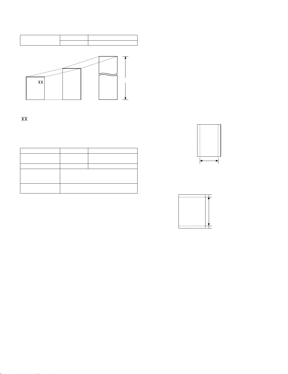
1. Document Sizes
Normal size Width 148 - 210 mm
Length 148 - 297 mm
(Max.)
5. Automatic Document Feeder Capacity
Number of pages that can be placed into the feeder at anytime is as
follows:
Normal size: max. ADF 20 pages
Special size: single sheet only (manual feed)
NOTE: • When you need to send or copy more pages than the feeder
limit, place additional pages in feeder when last page in feeder
is being scanned.
• Place additional pages carefully and gently in feeder.
If force is used, double-feeding or a document jam may result.
(Min.)
182mm
148mm 210mm
Use document carrier sheet for smaller documents.
• With special sizes, only one sheet can be fed into the machine at a
time. Insert next page into feeder as current page is being scanned.
(Max.)
A4 size
[Normal size]
297mm
216mm
[Special size]
356m
2. Paper Thickness & Weight
20 sheets 1 sheet(Manual)
Paper weight 21.5 lbs.
Paper thickness (ref.) 0.1 mm 0.1 mm ~ 0.18mm
Paper size LGL (216 mm x 355.6 mm)
Feeder capacity A4/LTR: 10 sheets max.
2)
(80 g/m
A4 (210 mm x 297 mm)
LTR (216 mm x 279 mm)
LGL : 1 sheet max.
14 lbs. ~ 42 lbs.
2
(52 g/m
~ 157g/m
2)
3. Document Types
• Normal paper
Documents handwritten in pencil (No. 2 lead or softer), fountain
pen, ball-point pen, or felt-tipped pen can be transmitted.
Documents of normal contrast duplicated by a copying machine
can also be transmitted.
• Diazo copy (blue print)
• Diazo copy documents of a normal contrast may be transmitted.
• Carbon copy
A carbon copy may be transmitted if its contrast is normal.
6. Readable Width & Length
The readable width and length of a document are slightly smaller than
the actual document size.
Note that characters or graphics outside the effective document scanning range will not be read.
• Readable width
208mm, max
Readable widt
• Readable length
This is the length of the document sent minus 4mm from the top
and bottom edges.
4mm
Readable length
4mm
4. Cautions on Transmitting Documents
• Documents written in yellow, greenish yellow, or light blue ink cannot be transmitted.
• Ink, glue, and correcting fluid on documents must be dry before the
documents can be transmitted.
• All clips, staples and pins must be removed from documents before
transmission.
• Patched (taped) documents should be copied first on a copier and
then the copies used for transmission.
• All documents should be fanned before insertion into the feeder to
prevent possible double feeds.
1 – 5
Page 7
[5] Installation
1. Site selection
Take the following points into consideration when selecting a site for
this model.
ENVIRONMENT
• The machine must be installed on a level surface.
• Keep the machine away from air conditioners, heaters, direct sunlight, and dust.
• Provide easy access to the front, back, and sides of the machine.
In particular, keep the area in front of the machine clear, or the original document may jam as it comes out after scanning.
• The temperature should be between 10 - 30°C.
• The humidity should be between 20% and 85% (without condensation).
ELECTRICITY: AC 220 - 230 V, 50 Hz, earthed AC outlet (U.K.,
Eire:230 V, 50 Hz, earthed (3-prong) outlet).
Caution!
• Connection to a power source other than that specified will cause
damage to the equipment and is not covered under the warranty.
• If your area experiences a high incidence of lightning or power
surges, we recommend that you install a surge protector for the
power and telephone lines. Surge protectors can be purchased at
most telephone specialty stores.
If the machine is moved from a cold to a warm place...
Condensation may form on the reading glass if machine is moved from
a cold to a warm place, this will prevent proper scanning of documents
for transmission. Turn on the power and wait approximately 2 hours
before using machine.
TELEPHONE JACK
A standard telephone jack must be located near the machine. This is
the telephone jack commonly used in most homes and offices.
• Plugging the fax machine into a jack which is not jack may result in
damage to the machine or your telephone system. If you do not
know what kind of jack you have, or need to have one installed,
contact the telephone company.
AM-400DE
2) Releasing the scanner.
Before plugging in the power cord, pull the scanner release toward
you to release the scanner lock.
• Caution: Plugging in the power cord without releasing the scan-
ner lock may damage the machine.
If you need to move the machine:
• In the event that you need to move the machine to a new location,
disconnect the telephone line cord before unplugging the power
cord. After you have unplugged the power cord, push the scanner
release back in to lock the scanner.
• After moving, release the scanner lock first and then plug in the
power cord. Connect the telephone line last.
3) Connecting the power cord.
Plug the power cord into a 220 - 230 V, 50 Hz, earthed AC outlet
(U.K., Eire:230 V, 50 Hz, earthed (3-prong) outlet).
• Caution: Make sure the scanner has been released as explained
on the previous page before plugging in the power cord.
• The power outlet must be installed near the equipment and must
be easily accessible.
Note: The shape of the power plug varies by country.
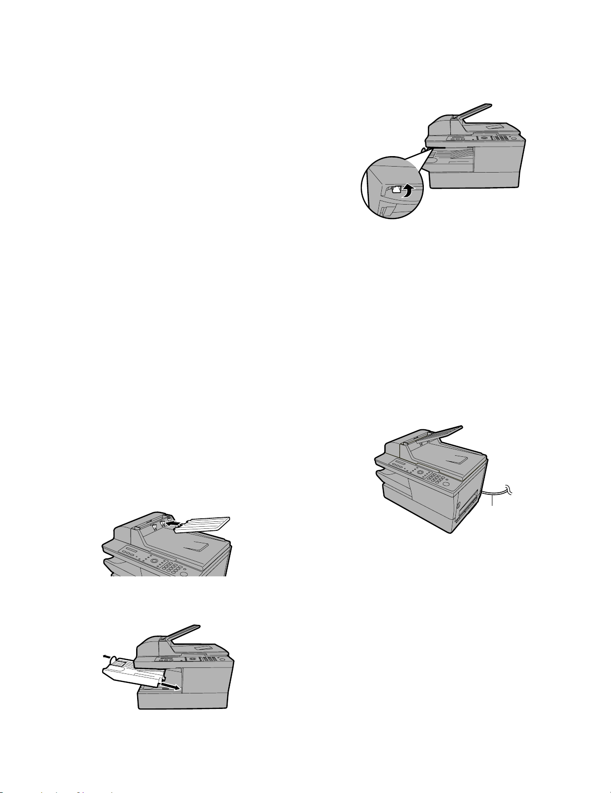
2. Attaching the trays
1) Attach the document feeder tray.
Slide the output tray into the machine as shown. When it stops, lift
the end slightly and push in so that the tray locks in place.
Important: The output tray must be attached correctly or the
machine will not operate.
POWER
CORD
• The machine does not have a power on/off switch. The power is
turned on and off by simply plugging in or unplugging the power
cord.
• Whenever you unplug the power cord, wait at least 5 seconds
before plugging it back in.
• If you area experiences a high incidence of lightning or power
surges, it is recommended that you install surge protectors for the
power and telephone lines. Surge protectors can be purchased
from your dealer or at most telephone specialty stores.
1 – 6
Page 8
AM-400DE
4) Connecting the telephone line cord.
Insert one end of the line cord into the socket on the back of the
machine marked TEL. LINE. Insert the other end into a wall telephone socket.
Note: The shape of the line cord plug varies by country.
• Italy: Use the provided adapter to connect the line cord to the wall
socket.
Make sure that the line cord is inserted into the TEL LINE socket.
Do not insert it into the TEL. SET socket!
1) Press the side cover release , open the side cover ,
and then open the front cover .
1
3
1
2
TEL.
LINE
TEL.
SET
• Germany: In Germany, the machine is supplied with a N-coded
line cable, enabling you to use an extension (cordless) telephone
on the same line. If you don’t have the standard NFN-outlet of
TELEKOM, you can purchase an NFN-adapter at your retailer.
Important: The facsimile function of this machine is not designed
for use on a line which has call waiting, call forwarding, or certain
other special services offered by your telephone company. If you
attempt to use the facsimile function in conjunction with any of
these services, you may experience errors during transmission and
reception of facsimile messages.
The facsimile function of this machine is not compatible with digital
telephone systems.
3
2
• Caution! The fusing unit inside the print compartment becomes
very hot during operation. Do not touch the inside of the print compartment after the machine has been in operation.
2) Remove the new drum cartridge from its packaging.
3) Insert the drum cartridge into the print compartment, sliding it along
the guides.
• Do not touch or allow other objects to contact the drum (the green
cylinder). This may damage the drum. If fingerprints, dust, or other
contaminants get on the drum, wipe it gently with a clean cloth.
• Exposure to light for more than several minutes will damage the
drum. Be sure to insert the drum cartridge promptly into the
machine.
• If you find it necessary to leave the cartridge out of the machine
for move than several minutes, wrap the cartridge in black paper.
3. Installing the toner cartridge and drum cartridge
The laser printer in the machine uses a toner cartridge and drum cartridge.
• The starter toner cartridge included with the machine can print
approximately 1,500 A4-size pages at 5% page coverage.
• When replacing the toner cartridge, use a SHARP AM-30DC toner
cartridge. One cartridge can print about 3,000 A4-size pages at 5%
coverage.
• The drum cartridge can print approximately 20,000 A4-size pages.
When replacing the drum cartridge, use a SHARP AM-90DR drum
cartridge.
Follow the steps below to install the toner cartridge and the drum cartridge.
Note: The quality of the toner cartridge is guaranteed for 18 months
after the date of manufacture indicated on the package. The quality of
the drum cartridge is guaranteed for 24 months after the date of manufacture indicated on the package.
Grasp this handle to
push the cartridge in.
4) Remove the new toner cartridge from its packaging. Shake the cartridge side to side four or five times to distribute the toner evenly
within the cartridge.
1 – 7
Page 9
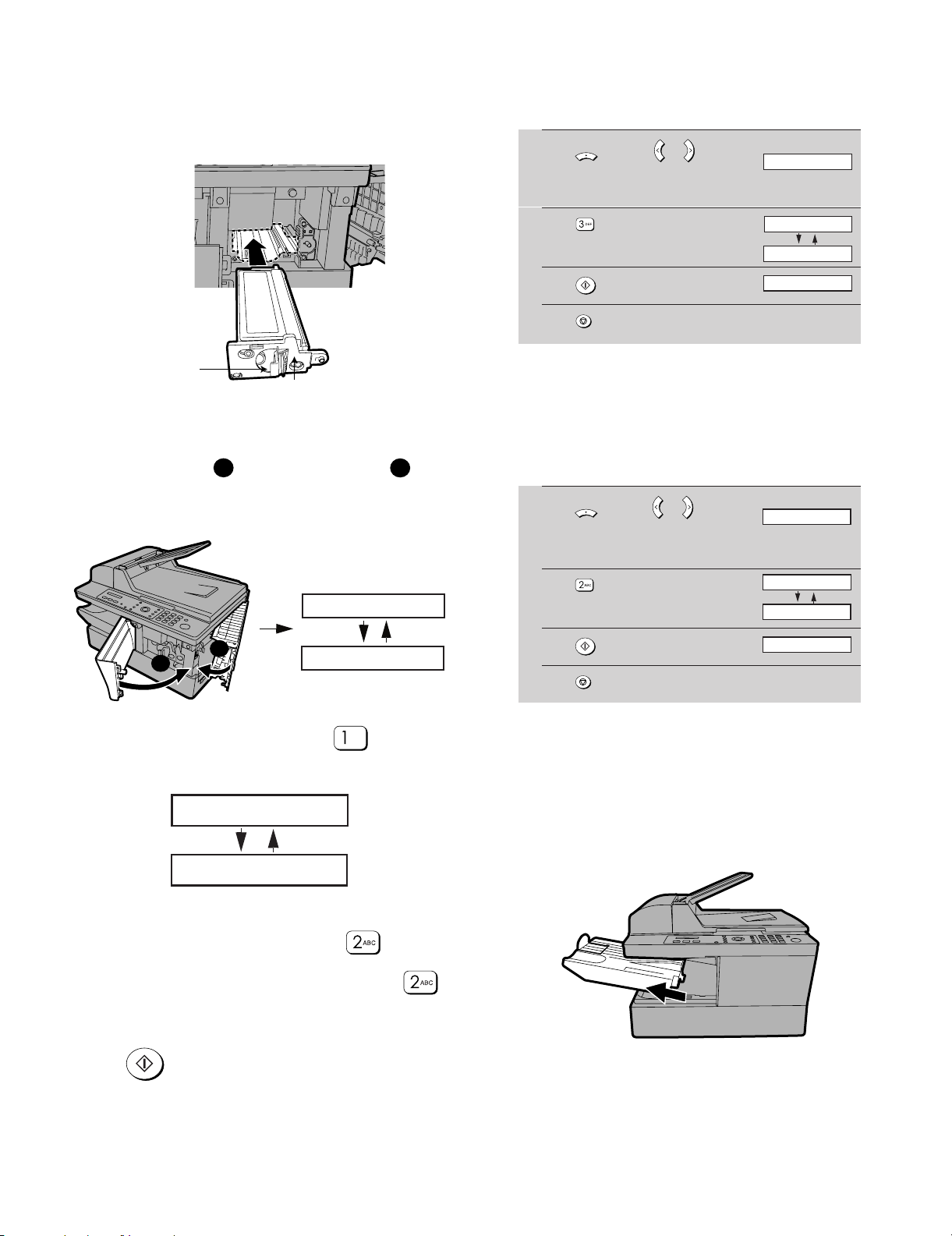
5) Grasp the cartridge handle and insert the toner cartridge into the
1 Press and then or
repeatedly until the display at right
appears.
MENU
Z
A
Display:
LIFE
2 Press .
3 Press .
4 Press repeatedly to exit.
CLEAR: START KEY
DRUM COUNTER
1: LIFE COUNTER
1 Press and then or
repeatedly until the display at right
appears.
2 Press .
3 Press .
4 Press repeatedly to exit.
MENU
Z
A
Display:
CLEAR: START KEY
LIFE
TONER COUNTER
3: CLR DRUM COUNT
print compartment, sliding it along the guides.
• After inserting the cartridge, press on the arrow mark to mark sure
it “clicks” into place.
• Do not touch the roller in the toner cartridge.
Grasp this
handle to
insert the
cartridge.
Press on this mark to
make sure the cartridge
"clicks" into place.
6) Close the front cover and then the side cover .
1
2
AM-400DE
4. Resetting the drum counter
Each time you install a new drum cartridge, follow the steps below to
reset the drum counter to zero.
5. Manually resetting the toner counter
When a new toner cartridge is installed, the toner counter is reset in
Step 7 on the previous page. The procedure below is normally not necessary; however, it can be used in the event that you need to reset the
toner manually.
• Make sure the side cover is completely closed. Otherwise, light
may enter the print compartment and damage the drum.
Display:
TONER EXCHANGED?
1
2
1=YES,2=NO
7) If you installed a new toner cartridge, press to select YES
(this will reset the toner counter to zero).
NEW TONER?
OK: PRESS START
• If you temporarily removed and then replaced an old toner car-
tridge for maintenance or other reason, press to continue
6. Loading paper
You can load approximately 250 sheets of A4 paper (80 g/cm2) in the
paper tray.
Caution! Do not use the blank side of paper that has already been
printed on.
1) Remove the output tray.
using the previous toner count. (Note: Be sure to press ,
or the machine will not alert you when the toner cartridge is out of
toner.)
8) Press .
9) If you installed a new drum cartridge, reset the drum counter as
explained below.
1 – 8
Page 10

AM-400DE
2) Insert a stack of paper into the tray, print side up.
• Important! The stack of paper must not be higher than the paper
height line on the paper tray.
Paper height line
3) Squeeze the sides of the paper guide as shown and slide it to the
slot for the length of the paper you are loading (A4).
4) Replace the output tray.
7. Installing the software
To use the machine as a printer and scanner for your computer, you
must install the software and connect a USB cable. The CD-ROM that
comes with the machine contains the following software:
• MFP Drivers: These consist of the printer driver that allows the
machine to be used as a printer, and the scanner driver that allows
you scan using TWAIN and WIA compliant applications.
• Sharpdesk: This is an integrated software environment that makes
it easy to manage image files and launch applications. (Note that
Internet Explorer
this is not installed, you will be prompted during the installation procedure to install Internet Explorer
• Button Manager: This allows you to initiate scanning from the
operation panel of the machine by selecting one of six preset scan
menus.
®
5.5 or higher is required to install Sharpdesk; if
®
6.0SP1 from the CD-ROM.)
Minimum system requirements
Operating system: Windows
®
Me / 2000 Professional/ XP
Port: USB 2.0 or 1.1 port
Display: 800 x 600 (SVGA) with 256 colors or more
Free hard-disk space: 150 MB or more
Other requirements: An environment in which the operating
system can freely operate.
Comments:
• USB 2.0 Hi-Speed is only possible if your computer has a USB 2.0
port and you are using a USB 2.0 cable. In addition, the Microsoft
USB 2.0 driver must be preinstalled in your computer, or the USB
2.0 driver for Windows
®
2000/XP provided through Windows
Update must be installed. Note that USB 2.0 Hi-Speed is not possible in Windows
®
Me.
• To scan the maximum document length (356 mm) using the auto
document feeder at 1200 dpi in full colour, at least 1GB of memory
is required. In addition, at least 600MB or more of free hard disk
space is required on the drive where your operating system is
installed. In Windows
®
Me, it is not possible to scan an A4 size
document at 1200 dpi in full color or grayscale (a lower resolution
or a smaller scanning area must be selected).
• Note for Windows
®
Me: In the Power Management settings in
the Control Panel, System stand-by must be set to Never. In
addition, do not use the stand-by feature that appears when you
shut down Windows.
Installing the software
• A USB cable is required to connect the machine to your computer.
Please purchase a USB 2.0 or USB 1.1 cable. The USB cable will
be connected during the software installation procedure. (If you
wish to use USB 2.0 Hi-Speed mode and your system meets the
requirements for Hi-Speed mode, purchase a USB 2.0 cable. A
USB 2.0 certified cable is recommended.)
• To install the software on Windows
you must log in with administrator’s rights.
• The windows shown in the following procedure appear in Win-
®
dows
XP. The windows that appear in other versions of Windows
may be slightly different.
Note: In the following instructions, “Windows 2000” indicates Windows 2000 Professional (the software cannot be installed on Windows 2000 Server).
1) Make sure that the USB cable is not connected to your com-
puter. (The cable will be connected in Step 11.)
• If the USB cable is connected, a Plug and Play window will
appear. Click the Cancel button to close the window and disconnect the cable.
2) Insert the Sharp CD-ROM into your computer’s CD-ROM drive.
3) In Windows
®
XP, click the start button, click My Computer, and
then double-click the CD-ROM icon.
®
In Windows
Me/2000, double-click My Computer on the desktop
and then double-click the CD-ROM icon.
4) Double-click the setup icon ( ) in the CD-ROM window.
5) The Language Selection window will appear. Select the language
that you wish to use and click Next. (The language selections vary
depending on your country or region.)
®
2000/XP using the installer,
1 – 9
Page 11

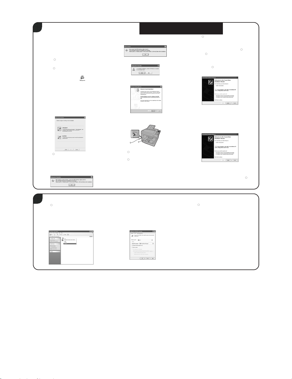
6) Follow the instructions in the windows that appear.
• When the Setup Type Selection window appears, select Standard to install all of the software components (this should normally
be selected). If you only wish to install certain components, select
Custom and then select the components that you wish to install.
Note: If you wish to select the folder where Sharpdesk and/or But-
ton Manager are installed, select Custom.
AM-400DE
10)The Search Setup Wizard will appear. Follow the on-screen
instructions to create an index database for Sharpdesk.
11)Make sure that the power cord of the machine is not plugged in
(the machine is powered off), and then connect the USB cable.
• Insert one end of the USB cable into the USB port on the machine
and the other end into your computer’s USB port.
Comments:
• Do not connect the AM-400 to a hub to which another AM-400 is
connected. If this is done, the AM-400 will not operate correctly.
• If you find that your computer does not recognize the machine or
operation is unstable, try connecting the USB cable to a different
USB port on your computer, or try a different USB cable (use the
shortest possible cable).
• In Windows
®
2000/XP, if a warning message appears at any time
regarding the Windows logo test or digital signature, be sure to
click Continue Anyway or Yes .
7) When the Finish window appears to indicate that the selected
packages have been installed, click Close.
8) If the installation was a Standard installation, the following window
will appear. Click OK.
• If you installed the MFP drivers using a Custom installation and
did not install Sharpdesk, the following window will appear. Click
OK and go to Step 11.
9) The following window will appear. Click Yes to restart your computer.
12)Plug in the power cord of the machine.
• Windows
®
XP: Go to the procedure for completing installation of
the software on Windows XP below.
• Windows
®
2000: This completes the installation of the software.
Note: If a warning message regarding the Windows logo test
appears (the warning may appear twice), click Yes each time the
window appears. This will complete the installation of the software.
• Windows
Completing installation of the software on Windows
®
Me: This completes the installation of the software.
®
XP
1 – 10
Page 12

AM-400DE
13)In Windows® XP, the Found New Hardware Wizard will appear.
Make sure that Install the software automatically (Recom-
mended) is selected and click Next (this will install software for
using the machine as a scanner).
14)When the wizard finishes installing the scanner software, click Fin-
ish to close the wizard.
15)After a brief interval, the Found New Hardware Wizard will appear
again to install software for using the machine as a printer. Make
sure that Install the software automatically (Recommended) is
selected and click Next.
• Note for Windows
first. Select No, not this time and click Next. Continue from the
previous window.
• If the following warning message appears regarding the Windows
logo test, click Continue Anyway.
®
XP SP2: The following window will appear
• If the following warning appears regarding the Windows logo test,
click Continue Anyway.
1 – 11
Page 13
16)When the wizard finishes installing the printer software, click Finish
to close the Wizard. This completes the installation of the software
on Windows
®
XP.
Sharpdesk online guide
For information on using Sharpdesk, view the Sharpdesk online
guide on the CD-ROM. To view the online guide, open the Manual
folder and then the EnglishA folder on the CD-ROM, and doubleclick SDUG_Enu.pdf.
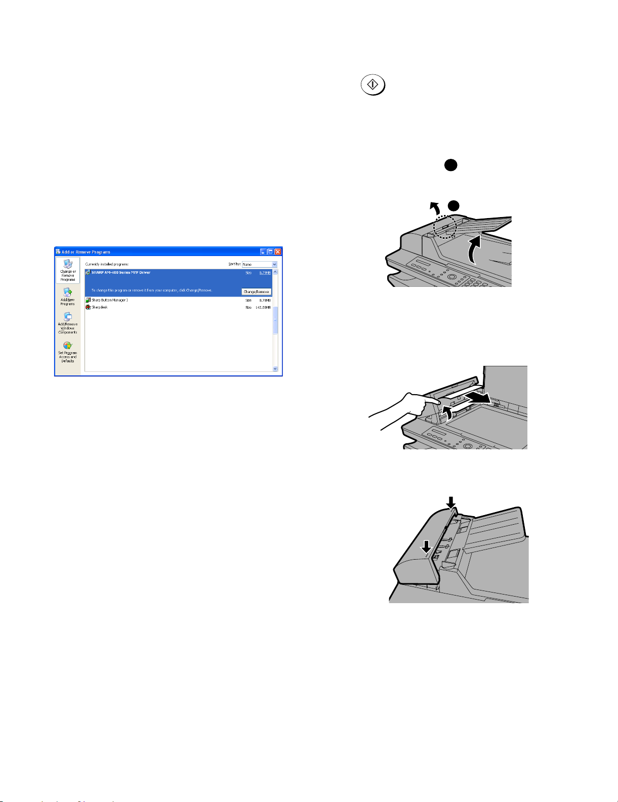
Removing the software
In the event that you need to remove the software from your computer, follow the steps below.
1) Disconnect the USB cable from your computer and the machine.
2) Open the Control Panel and select Add or Remove Programs
(or Add/Remove Programs).
3) Select SHARP AM-400 Series MFP Driver (or Sharpdesk)
from the list, and click the Change/Remove button (or the Add/
Remove button).
AM-400DE
8. Clearing a jammed document
If the original document doesn’t feed properly during transmission or
copying, or DOCUMENT JAMMED appears in the display, first try
pressing . If the document doesn’t feed out, open the auto
document feeder cover and remove it.
Important:
Do not try to remove a document without opening the auto document
feeder cover. This may damage the feeder mechanism.
1) Squeeze the cover release and open the auto document
feeder cover. Open the document glass cover.
1
1
4) Click OK to confirm the removal.
2) Remove the document.
• The document can be removed from either the top or the bottom
slot, whichever is easiest.
3) Close the auto document feeder cover, pressing down on both
sides to make sure it clicks into place.
Press down
on the marks
1 – 12
Page 14

AM-400DE
1
2
9. Clearing jammed printing paper
4) If the jammed page cannot be pulled out directly, open the front
1) Press the side cover release and then open the side cover
2
.
2) Push the two heater roller release levers down to release the
heater roller.
• Caution! The fusing unit (indicated in white at right) becomes
very hot during operation. Do not touch the fusing unit.
1
1
2
cover and rotate the white knob in the direction
shown to feed the jammed page out into the output tray.
2
1
5) After the jammed page has been removed, push the two heater
roller release levers back up.
2
3) If the jammed page is protruding from the side of the machine, gently pull it out. Take care not to tear the paper or leave any torn
pieces of paper in the print compartment.
• If this clears the jam, go to Step 5.
• If you are unable to clear the jam in this way, go to Step 4.
• Take care not to touch or allow other objects to contact the drum
(the green cylinder). This damage the drum.
6) Close the front cover (if you opened it) and then the side
cover .
1
2
1
Note: If you find that another paper jam occurs immediately after
clearing a paper jam, open the side cover and then the front cover
and remove the jammed paper as explained above. With the front
cover and side cover still open, remove the output tray and remove
the printing paper from the paper tray. Replace the output tray and
close the front cover and then the side cover. Remove the output
tray once again, fan printing paper, replace it in the paper tray, and
then replace the output tray.
1 – 13
Page 15

10. Troubleshooting
1. Display
ADD PAPER Check the printing paper. If the tray is empty, add
BYPASS MISFEED The paper is not inserted correctly in the bypass tray.
BYPASS PAPER! /
IF COPY, PRESS
(alternating messages)
CHK SCANNER LOCK/
PLS RETURN POWER
(asternating messages)
COVER OPEN One or both of the print compartment covers are
DATE/TIME UNSET The date and time need to be set. Note
DOCUMENT JAMMED The original document is jammed. See the following
DOCUMENT READY A document has been inserted in the auto document
DRUM LIFE OVER This appears when the drum cartridge needs
FAX RX IN MEMORY A fax has been received in memory because the
GRP. SPACE FULL This appears if you attempt to store a Group when
LINE ERROR Transmission or reception was not successful. Press
MEMORY IS FULL If faxes have been received to memor y because
NO # STORED This appears if you attempt to search for a Speed Dial
OFF HOOK This appears when an extension phone connected as
paper. If there is paper in the tray, make sure it is
inserted correctly (take out the stack, align the edges
evenly, and then reinsert it in the tray). Printing will
resume automatically when the output tray is
replaced.
Remove the paper and insert it again.
Paper has been inserted in the bypass tray. If the
paper has been inserted for a copy job, press to
set the paper size. If the paper is for a print job, the
message can be disregarded.
Make sure that the scanner lock has been released
and then unplug the power cord, wait at least 5
seconds, and plug it back in.
open. Make sure both covers are closed.
that the date and time settings will be lost if the
machine is unplugged or a power failure occurs.
section, Clearing Paper Jams. Document jams will
occurifyouloadmorethan20pagesatonceorload
documents that are too thick.
The document may also jam if the receiving machine
doesn’t respond properly when you attempt to send a
fax.
feeder and the machine is waiting for you to begin
faxing or copying.
replacement.
toner cartridge needs replacement, you have run out
of printing paper, the paper is jammed, or paper is
inserted in the bypass tray. The fax will print out
automatically when the problem is fixed.
both Groups are already programmed.
the STOP key to clear the message and then try
again. If the error persists, see Line error.
printing is not possible (an additional message will
indicate the problem), resolve the problem so that
printing can continue (see Substitute Reception to
Memory)
If you are attempting to send a fax, see If the memory
becomes full.
If you are copying, see If MEMORY IS FULL appears.
number when none have been stored.
explained is lifted. Only can be pressed in
fax mode when this message appears.
REMOVE /
BYPASS PAPER
(alternating messages)
SYSTEM ERROR [XX]
(a number appears in
“XX”)
(Refer to Printer error code/
Scanner message)
SET BYPASS PAPER /
A
SIZE: XXXX
(alternating messages; a
paper size appears in
“XXXX”)
TONER EMPTY The toner cartridge must be replaced. Printing will be
TONER NEAR EMPTY The toner cartridge is almost out of toner
TOTAL PAGE(S) 01 Number of fax pages transmitted or received.
A fax has been received to memory because paper is
inserted in the bypass tray (faxes cannot be printed
while paper is in the bypass tray). Remove the paper
from the bypass tray to allow the fax to be printed.
If this message appears, unplug the power cord, wait
about 10 seconds, and then plug it back in. If the
message still appears, unplug the power cord and call
for service.
Paper must be inserted in the bypass tray for a print
job or copy job that requires use of the bypass tray.
Insert the indicated size of paper in the tray.
possible (although the output will be increasingly
faint) until a fax is received. Once a fax is received, it
will be held in memory and printing will not be
possible until the toner cartridge is replaced.
(approximately 200 pages can be printed).
2. Audible signals
Continuous tone 3 seconds Indicates the end of transmission or
Intermittent tone
(3 beeps)
Rapid intermittent
tone
5 seconds
(1 second on, 1
second off)
35 seconds
(0.7 seconds on,
0.3 seconds off)
reception.
Indicates incomplete transmission or
reception.
Indicates that an extension phone
connected as explained is off hook.
3. Printer error code (Troubleshooting Refer to page 5-27 to 5-29)
PAPER JAM The roller sensor could not detect its home position
SYSTEM ERROR [P2]
SYSTEM ERROR [P3]
SYSTEM ERROR [P4] ROM or RAM error was detected on the printer
SYSTEM ERROR [P5] High temperature error was detected.
SYSTEM ERROR [P6] Low temperature error was detected.
SYSTEM ERROR [P7]
after driving the pick up motor for the specified period.
The roller sensor could not become NOT-Active after
passing the specified period from picking up paper.
The printer controller detected the optical unit (LSU)
error.
The external interrupt signal for optical unit (LSU) or
High-voltage control did not become active after
passing the specified period.
Thermistor error was detected.
control unit.
Communication error between the main controller
and the printer controller was detected.
AM-400DE
OUTPUT TRAY OFF The output tray is not attached correctly. Attach it as
PAPER JAMMED The printing paper is jammed.
PAPER MISMATCHED This appears after printing if the size of the printed
explained. The machine will not operate if the output
tray is not attached correctly.
image did not match the paper size on some pages
of the job. Check the printed pages and reprint as
needed.
4. Scanner message (Troubleshooting Refer to page 5-29)
CHK SCANNER LOCK The scanner unit could not detect change point of
home postion. (ON-> OFF or OFF->ON)
1 – 14
Page 16

AM-400DE
11. Quick setup guide
For detailed instructions
on setting up and using the AM-400, see the
online guide on the CD-ROM.
To open the guide, double-click the Manual folder on
the CD-ROM, double-click English, and then doubleclick Online Manual.pdf.
(Note: Acrobat Reader 5.05 or higher is required to
view the manual.To install Version 5.05, double-click
Acrobat Reader, English, and then ar505enu.exe
on the CD-ROM.)
All company names and product names appearing in this
setup guide are the trademarks of their respective owners.
Important:
3
Pull the scanner release toward you to
release the scanner lock.
Caution: Be sure to release the scanner lock
before plugging in the power cord.
Install the toner cartridge and drum cartridge.
6
1. Press
5. Insert the toner cartridge, sliding it along
1
ı
. Open the side cover
2
and then the front cover .
ı
3
3
ı
1
Caution!
Do not touch the fusing unit
under the side cover after the
2
machine has been in operation,
as it may become very hot.
the guides until it clicks into place.
Press on the arrow
mark to make sure
the cartridge clicks
into place
Make sure you have the following items. If any
1
are missing, contact your dealer or retailer.
Note: The shape of the line cord plug varies by
country. An adapter (not shown) is provided in
some countr ies.
Telephoneline
cord
Output tray
Plug the powercord into a standard,ear thed
4
power outlet.
Note: The power outlet must be installed
near the equipment and must be easily
accessible.
Note: The
shape of the
power plug
varies by
country
2. Remove the drum cartridge from its
packaging.
6. Close the front coverıand
then the side cover
1
2
Document
feeder tray
1
ı
2
ˇ
.
ı
Toner
cartridge
Display:
TONER EXCHANGED?
1:YES, 2:NO
Drum
cartridge
Setup
CD-ROM
Guide
3. Inser t the drum cartridge,
sliding it along the guides.
Grasp this handle to
push the cartridge in
7. Press
to select
then press . (This resets
the toner cartr idge counter.)
2
When the tray
stops, lift the
end slightly
and push in.
5
Note: The
shape of the
line cord plug
varies by
country.
"YES" and
Attach the trays.
Connect the phone line cord
to the TEL. LINE jack and a wall jack.
Italy: Use the provided adapter to connect the
line cord to the wall socket.
T
EL.
LINE
TE
L.
S
E
T
4. Remove the toner cartridge from its
packaging. Shake the car tridge side
to side four or five times to distribute
the toner evenly within the
cartridge.
8. Reset the drum car tridge counter :
MENU
a.Press
A
display.
b. Press and then .
c. Press repeatedly to exit.
once and then or
until "LIFE" appears in the
Z
Load paper.
7
1. Remove the output tray.
3. Squeeze the sides of the paper
guide and slide it to the slot for
the length of paper loaded.
2. Inser t a stack of paper
into the tray, print side up.
The stack should
not be higher
than this line
4. Replace the output tray.
Set the date and time that appear
8
in the fax mode display.
1. In the date and time display of faxmode
FAX
(press if needed to select fax
mode), press , , .
2. Enter a two-digit number for the day
("01" to "31").
MENU
Example: the 5th
•
To clear a mistake press .
Z
3. Enter a 2-digit number for the month.
Example: February
4. Enter the year (four digits)
Example:
1 – 15
5. Enter a two-digit number for the hour
(00 to 23) and a two-digit number for
the minute (00 to 59).
Example: 9:25
6. Press .
ENTER
7. Press repeatedly to exit.
Page 17
AM-400DE
Install the software on your computer. (The software
9
allows the machine to be used as a printer and scanner.)
1. Make sure that a USB cable is not connected
to the machine and your computer. (The cable
will be connected in Step 11.)
•
If a cable is connected and a Plug and Play window appears, close
the window and disconnect the cable.
2. Insert the Sharp CD-ROM into your computer's
CD-ROM drive.
3. Windows
R
XP: Click the start button, click My
Computer, and double-click the CD-ROM icon.
R
Windows Me/2000: Double click
the desktop and double-click the CD-ROM icon.
My Computer
4. Double-click the setup icon ( ) in the CD-
ROM window.
5. If the Language Selection window appears,
select the language that you wish to use and click
Next (the language selections will vary depending
on your country or region).
6. Follow the on-screen instructions.
• When the Setup Type Selection window appears, select
Standard to install all of the software components (this should
normally be selected). If you only wish to install certain
components, select Custom and then select the components
that you wish to install.
•
7. When the
8. If the installation was a Standard installation, the
R
In Windows 2000/XP, if a warning message appears at any time
regarding the Windows logo test or digital signature, be sure to click
Continue AnywayorYes
selected packages have been installed, click
following window will appear. Click OK.
.
Finish
window appears to indicate that the
Close
Note: A USB 2.0 or 1.1 cable is required to connect the
machine to your computer. Please purchase this separately.
•
If you installed the MFP drivers using a
and did not install Sharpdesk, the following window will
OK
appear. Click
9.
The following window will appear. Click Yes to restart
your computer.
and go to Step 11.
on
10. The Search Setup Wizard will appear. Follow the
on-screen instructions to create an index
database for Sharpdesk.
11. Make sure that the machine's power cord is not
plugged in, and then connect the USB cable to the
USB port on the machine and on your computer.
12. Plug in the machine's power cord.
• Windows XP: Follow Steps 13 through 16 to
• Windows 2000: This completes the installation of the
.
R
complete the installation of the software.
R
software.
Note:
If a warning message regarding the Windows logo
test appears (the warning may appear twice), click
each time the window appears. This will complete the
installation of the software.
Custom
installation
Yes
• Windows Me: This completes the installation of the
Completing the installation on Windows XP
13. In Windows XP, the Found New Hardware
• If a warning message appears regarding the Windows
14. When the wizard finishes installing the software, click
15. After a brief interval, the Found New Hardware
• If a warning message appears regarding the Windows
16. When the wizard finishes installing the software,
R
software.
Note:
In the power management settings in the
Panel
,
System stand by
Wizard will appear. Make sure that Install the
software automatically (Recommended) is
selected and click Next.
Note for Windows XP SP2
wizard will ask you if the wizard can connect to Windows
Update. Select
logo test, click Continue Anyway.
Finish to close the wizard.
Wizard will appear again. Make sure that Install
the software automatically (Recommended) is
selected and click Next.
logo test, click Continue Anyway.
click Finish to close the wizard. This completes
the installation of the software on Windows XP.
must be set to
R
R
No, not this time
: The first window of the
and click
Never
R
Next
Control
.
.
R
Configure Button Manager (one of the programs installed in the above step) as
10
the program on your computer that handles scanner events from the machine.
R
Windows XP/Me
1. Click the start button, click Control Panel,and
double-click Scanners and Cameras.
•
If
Scanners and Cameras
click view all Control Panel options
Me,
2. Right-click the SHARP AM-400 icon and
select Properties.
does not appear in Windows
.
3. The SHARP AM-400 Properties appear.
Click on the Events tab.
4. Select SC1 from the Select an event list.
5. In the Actions field, select Start this program
and then select Sharp Button Manager I from the
list of programs. Click Apply.
6. Repeat Steps 4 and 5 for each of events SC2
through SC6. When finished, click the OK button.
R
Windows 2000
1. Click the Star t button, point to Settings,and
select Control Panel.
2. In the Control Panel, double-click Scanners and
Cameras.
3. Select SHARP AM-400 and click Properties.
4. Click the Event s tab in the SHARP AM-400
Properties.
5. Select SC1 from the Scanner events list.
6. In Send to this application,selectSharp
Button Manager I.
• If other applications appear in the list, make sure that
none are selected.
7. Click the Apply button.
8. Repeat Steps 5 through 7 for each of events SC2
through SC6. When finished, click the OK button.
1 – 16
Page 18

AM-400DE
AM-400DE
CHAPTER 2. ADJUSTMENTS
[1] Adjustments
1. General
Since the following adjustments and settings are provided for this
model, make adjustments and/or setup as necessary.
2. Adjustments of output voltage (FACTORY ONLY)
1. Install the power supply unit in the machine.
2. Set the recording paper and document.
3. When the document is loaded, power is supplied to the output
lines. Confirm that outputs are within the limits below.
2.1. Output voltage settings
Service Manual
CNLSR
CNPM
CNHV
CNMM
CNPUM
CNTCT
CNFM
CNROLSNS
CNTCVR
CNBYPE
CNPIN
CNPW
1
FUSING UNIT
CNRTH
CNOUT1
CNOUT2
CONTROL PWB
(TOP SIDE)
14
CNHT
3
1
THERMAL
FUSE-2
CNSCM
CNCIS
CNLIU
CN6
3
1
1
1
2
CN2
POWER SUPPLY
PWB (TOP SIDE)
INTERLOCK
SWITCH
CNPN
CNORG
CNHPS
CNUSB
CNPW
CNFRT
CNSP
14
Output Voltage limits
+24VSUB 23.04V~24.96V
+24VMAIN 23.04V~24.96V
+5VMAIN 4.75V~5.25V
+3.3VMAIN 3.201V~3.399V
Connector CNPW
Pin No.
1
2
3
4
5 +24VMAIN
6 +24VMAIN
7DG
8
9
10
11
12
13
14
Connector
Pin No.
1
2
3
Connector
Pin No.
1
2
3
Connector
Pin No.
1
2
CNPW
MG
+24VSUB
MG
MG
+5VMAIN
DG
+3.3VMAIN
DG
/HEATER ON
/PWRLY
/ZC
CN6
+24VMAIN
N.C.
+24VS
CNHT
N
N.C.
L
CN2
1
2
2 – 1
Page 19

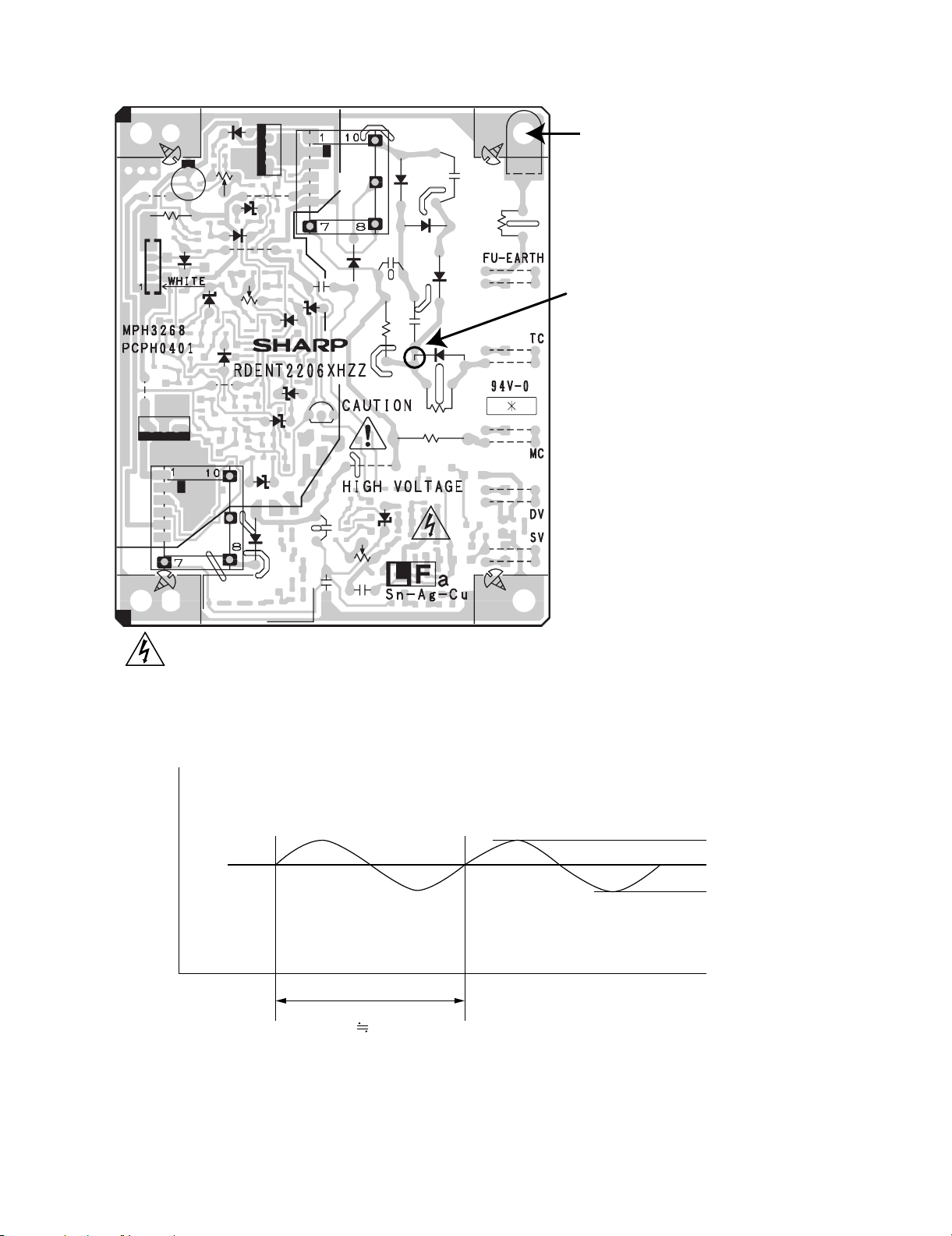
3. High voltage power check
3.1. General
Note: Since the parts of this PWB cannot be supplied, change it as a unit.
CAUTION
DO NOT TOUCH!
CN1
CN3
(VR51)
Q3
D3
D10
J1
QJ005
VR1
D1
D58
J6
D2
D8
J3
VR51
D61
D62
D60
D52
D54
C1
J5
R1
J2
Q52
B51
C9
Q38
B1
QJ071
D9
D53
J4
C56
C65
VR31
C31
CAUTION HIGH VOLTAGE AREA MAX. 4000V
D4
C6
CN4
R93
D5
C5
J52
J51
R15
C7
D7
R16
R67
D31
J12
J11
J22
J21
J42
J41
J32
J31
CAUTION - HIGH VOLTAGE
The unit's back cover should never be opened by
anyone other than a qualified serviceperson.
There are many high voltage parts inside the unit,
and touching them is dangerous.
AM-400DE
CAUTION HIGH VOLTAGE AREA MAX. 4000V
R10
R3
R9
R8
R3
C2
R44
R65
R66
R59
R94
R5
R98
R6
C55
R60
C52
R43
R74
R73
R103
R80
R79
R81
Q34
D42
R42
D41
R102
Q31
D59
Q33
Q32
D57 D56 D55
Q35
R32 R31
R41
R78
Q36
C32
R36
R34
R33 R35
R72
R71
R40
R70
R39
R38
Q37
R37
R86
IC1
C8
R92
R61
C53
R58
R75
R101
R69
R46
R76
R77
R83
R84
R85
R87
R88 R89 R90
C4
R13
R14
R7
R91
C54
R66
R11
R4
R18
R14
R47
Q51
R3
Q1
R19
R63
R53
R100
CN1
C61
R51
Q57
R54
R52
C62
R55
C51
CAUTION - HIGH VOLTAGE
The unit's back cover should never be opened by
anyone other than a qualified serviceperson.
There are many high voltage parts inside the unit,
and touching them is dangerous.
R2
R17
R57
R56
R99
C66
R48
Q58
R62
R50
R49
R64
2 – 2
Page 20

AM-400DE
3.2. MC Voltage Check Point
D3
CN3
CN1
C1
J5
R1
J2
Q52
VR1
D8
D10
VR51
D1
D58
J1
QJ005
B51
J3
D60
D52
Q3
B1
GND (-)
D4
C6
D5
C7
D7
R16
R67
D61
QJ071
C9
Q38
D53
D9
J4
C56
C5
R15
D31
VR31
J6
D2
D62
D54
J52
J11
J41
J51
J12
J22
J21
J42
J32
J31
CN4
R93
MC Voltage Check Point (-)
(There is danger of an electric shock!)
Use Measuring instrument:
Input Resistance : more than 100 MΩ
Maximum Voltage : more than 2 kV
VOLTAGE
MC:-950V±20V(PRINTING)
MC:-850V±20V(CLEANING)
C65
C31
1) MC Voltage
Voltage(v)
CAUTION - HIGH VOLTAGE
The unit's back cover should never be opened by anyone other than
a qualified serviceperson. There are many high voltage parts inside
the unit, and touching them is dangerous.
300Hz
Time(s)
Type
-570V
-950V
-1330V
Tolerance
± 67V
± 20V
± 67V
2 – 3
Page 21
3.3. TC Voltage Check Point
D3
CN3
CN1
C1
J5
R1
J2
Q52
VR1
D8
D10
D1
D58
J1
QJ005
B51
VR51
J3
D60
D52
AM-400DE
Q3
J6
D2
D61
D62
D54
QJ071
C9
Q38
D53
D9
C56
B1
GND (-)
D4
R15
C6
D5
C5
C7
D7
J52
J11
J51
J12
CN4
R93
TC Voltage Check Point (+)
(There is danger of an electric shock!)
Use High Voltage Tester:
Requirement of Measuring instrument:
Input Resistance : more than 100 MΩ
Maximum Voltage : more than 5 kV
R16
J22
R67
J4
D31
VR31
J21
J42
J41
J32
J31
VOLTAGE
TC(+):+3600V±72V(PRINTING)
TC(-):-500V±50V(CLEANING)
1) TC Voltage
Voltage(v)
C65
C31
CAUTION - HIGH VOLTAGE
The unit's back cover should never be opened by anyone other than
a qualified serviceperson. There are many high voltage parts inside
the unit, and touching them is dangerous.
300Hz
Type
-3980V
-3600V
-3220V
Time(s)
Tolerance
± 72V
2 – 4
Page 22

AM-400DE
3.4. SV/DV Voltage Check Point and SV (-) Voltage Adjustment Volume
Q3
CN3
CN1
D3
VR1
C1
J5
R1
D10
D58
J1
J2
Q52
J6
D2
D8
J3
VR51
D1
D60
C9
D61
D62
D52
QJ005
B51
D54
CAUTION - HIGH VOLTAGE
The unit's back cover should never be opened by anyone other than
a qualified serviceperson. There are many high voltage parts inside
the unit, and touching them is dangerous.
QJ071
D9
D53
Q38
J4
C56
C65
B1
VR31
C31
R15
D31
D4
C6
R93
D5
C5
J52
J51
C7
D7
R16
R67
J12
J11
J22
J21
J42
J41
J32
J31
GND (-)
CN4
DV Voltage Check Point (+)
VOLTAGE
DV(+):+300V±5V(CLEANING)
DV(-):-220V±5V(PRINTING)
SV Voltage Check Point (+)
VOLTAGE
SV(+):+400V±15V(CLEANING)
SV(-):-320V±15V(PRINTING)
DV (-) Voltage adjustment Volume
VR31
It can be made to change with VR31.
In the range of ± 50V.
DV(-):-220V±50V(PRINTING)
2 – 5
Page 23

4. IC protectors replacement
1 Make sure that the date and time
display of fax mode appears (if needed
press ) and then press .
2 Press .
3 Press (Press in Russia and
Poland).
4 Press a number key to select the
desired volume setting:
:HIGH
: MIDDLE
:LOW
:OFF
5 Press repeatedly to exit.
FAX
MENU
Display:
1: DATE&TIME SET
FAX SETTING
1: HIGH
The display briefly shows
your selection, then:
4: ALARM VOLUME
ICPs (IC Protectors) are installed to protect the CIS unit, LIU PWB
unit, Scanner motor drive circuit, Pickup motor drive circuit, Main
motor drive circuit and IC22 circuit. ICPs protect various ICs and electronic circuits from an overcurrent condition.
The location of ICPs are shown below:
AM-400DE
5. Settings
5.1. Dial mode selector
DIAL mode (Soft Switch No. SW5 Data No. 5)
Setting is not required since the required mode is TONE ONLY.
6. Volume setting
CNLSR
F5
CNPM
F7
CNHV
CNMM
CNPUM
F6
CNTCT
CNFM
CNROLSNS
CNTCVR
CNBYPE
CNPIN
F6/F8:Top side F3/F4/F5/F7:Bottom side
1) F8 (KAB5002 201) is installed in order to protect IC’s from an
overcurrent generated in the CIS unit. If F8 is open, replace it with a
new one.
2) F4 (KAB5002 251) is installed in order to protect IC’s from an
overcurrent generated in the LIU PWB unit. If F4 is open, replace it
with a new one.
3) F3 (KAB3202 202) is installed in order to protect IC’s from an
overcurrent generated in the scanner motor drive circuit. If F3 is
open, replace it with a new one.
4) F5 (KAB5002 251) is installed in order to protect IC’s from an
overcurrent generated in the IC22 circuit. If F5 is open, replace it
with a new one.
5) F6 (KAB3202 102) is installed in order to protect IC’s from an
overcurrent generated in the pickup motor drive circuit. If F6 is
open, replace it with a new one.
6) F7 (KAB2402 402) is installed in order to protect IC’s from an
overcurrent generated in the main motor drive circuit. If F7 is open,
replace it with a new one.
In addition to the replacement of F3, F4, F5, F6, F7 and F8, the factor causing F3, F4, F5, F6, F7 and F8 to open must also be
repaired. If not, F3, F4, F5, F6, F7 and F8 will open again.
Replacement parts
KAB3202 202 (Sharp code: QFS-L1027YCZZ)
KAB5002 251 (Sharp code: QFS-L2021XHZZ)
KAB3202 102 (Sharp code: QFS-L0004QCZZ)
KAB2402 402 (Sharp code: QFS-L2025XHZZ)
KAB5002 201 (Sharp code: QFS-L2016XHZZ)
CNRTH
CNOUT2
CONTROL PWB
CNPW
CNCIS
CNOUT1
(TOP SIDE)
F4
F8
CNSCM
F3
CNIU
CNPN
CNFRT
CNORG
CNHPS
CNSP
CNUSB
6.1. Ringer
Like a telephone, the machine will ring to alert you when a call comes
in. To adjust the volume of the ringer or turn it off, follow the steps
below.
6.2. Alarm volume
The machine sounds a three-beep alarm to alert you when an error
occurs during fax transmission or reception. To adjust the volume of
the alarm or turn it off, follow the steps below.
1 Make sure that the date and time
display of fax mode appears (if needed
FAX
press ) and then press .
MENU
2 Press .
3 Press (Press in Russia and
Poland).
4 Press a number key to select the
desired volume setting:
:HIGH
:LOW
:OFF
Display:
FAX SETTING
1: DATE&TIME SET
1: HIGH
The display briefly shows
your selection, then:
1: DATE&TIME SET
5 Press repeatedly to exit.
2 – 6
Page 24

AM-400DE
Press
, and
the
following
display will appear.
MENU
9 8
6
M/C Ver:TE53
(Diag•specifications)
MENU
9 8 6
ENTER SINGLE PRINT
ENTER CONTINUOUS PRINT
ENTER
COPY AGING
ENTER
LIFE MODE
ENTER
TOP VOID ADJUST
ENTER
PRINT ADJUST
ENTER
TEST MODE
START
START
ENTER
Then press the
key. Select the desired item with the
key and the key or select with the rapid key.
Enter the mode with the key.
PRINT DIAG MODE
: PRINTER ROM version
M/C Ver:TE53
(The alternate display of two screens.)
MEMORY CLEAR
1:CLEAR
[1]Key
[2]Key
Stand-by display
[2] Diagnostics and service soft switches
1. Entering the diagnostic mode
1.1. Fax diagnosis
This diagnosis is concerned with the main body of fax which is used
for production and service support.
Entering the diagnostic mode
1.2. Print diagnosis
This diagnosis is concerned with the print which is used for production
and service support.
Entering the diagnostic mode
Press
MENU
9 8
display will appear.
TE37 / x x x x (AM-400DE) or
TE44 / x x x x (AM-400IT) or
TE42 / x x x x (AM-400H)
Then press the
START
TE39 / x x x x (AM-400F) or
TE48 / x x x x (AM-400SE) or
: FAX ROM version
xxxx:Checksum
key. Select the desired item with the
and the key or select with the rapid key.
Enter the mode with the
(Diag
•
specifications)
9 8 7
MENU
ENTER
ENTER
ENTER
ENTER
ENTER
ENTER
ENTER key.
DIAG MODE COUNTRY NAME
SOFT SWITCH MODE
ROM & RAM CHECK
PANEL CHECK MODE
CHECK PATTERN MODE
SIGNAL SEND MODE 1
SIGNAL SEND MODE 2
TE37 / x x x x or
TE39 / x x x x or
TE44 / x x x x or
TE48 / x x x x or
TE42 / x x x x
(The alternate display of three screens.)
START
7
,and
the
following
key
Memory clear when power is turned on
Pressing the START and STOP keys, turn on the main power, and the
following message will be indicated.
ENTER
ENTER
ENTER
ENTER
ENTER
ENTER
ENTER
ENTER
MEMORY CLEAR
CIS ADJUSTING MODE
DIAL TEST MODE
AUTO FEEDER MODE
FLASH MEMORY TEST
GEAR CHANGE MODE
FLATBED AGING
MESSAGE PRINT (AM-400DE/F/IT/SE only)
MEMORY CLEARING
When 1 is selected, the memory will be cleared to be ready to operation.
If 2 is selected, memory will not be cleared and the machine enters
standby mode.
2 – 7
Page 25

2. Diagnostic items description
ROM& RAM CHECK
ROM = RAM=
Start checking
by pressing [ENTER] key
ROM=OK,RAM =OK
PRINTING
ALL KEY OK !!
2.1. Fax diagnosis
2.1.1 Soft switch mode
In this mode, the soft switches are set and the soft switch list is printed.
1. Operation
Soft switch mode screen
SOFTSWITCH MODE
[ENTER] Key
SW01=01010010
Switch No.
2. Switch number selection and data setting
1) Enter two digits of a soft switch number to set the switch num-
ber. Of a switch number of non-existing soft switch is entered,
key error buzzer sounds to reject the input.
SW01=01010010
cursor position
2) Press [ENTER] key for setting of the next soft switch.
12345678:DataNo.
SW01 =
[1]key
SW16=01010010
[ 6] key
AM-400DE
5. Storage of data
In the following cases, the data if the soft switches set will be
stored.
• It is shifted to set the next soft switch by pressing [ENTER] key.
• It is shifted to set the next soft switch with the [>] key.
• It is shifted to the last soft switch with the [<] key.
• It is shifted to set another soft switch by inputting two digits as
the switch number.
• Output of the soft switch list starts.
6. Protocol monitor
If the SW No. 8 Data No. 5 is set to 1, the protocol monitor result is
printed after fax communication.
2.1.2 ROM & RAM check
To check the sum value of Firmware or RAM.
No. Device Alarm Buzzer Remarks
1
2 D-RAM1(*1) 2 times <Short
*1 WORK MEMORY (SDRAM 16M).
1. Display
ROM
(PROGRAM FLASH)
Main
1 time <Short
sound>
sounds>
SW01=01010010
cursor position
[ENTER]Key
SW02=01001100
SW03=01001100
[ENTER]Key
3) Data number selection
(a) Pressing [>] key moves the cursor to the right.
If the cursor is on data number 8, pressing [>] key shifts the cursor to data number 1 of the next switch number. If the switch
number is the final, pressing [>] key will exit the soft switch
mode.
SW01=01010010
cursor position
SW02=01001100
[>]Key
SW03=01001100
with the cursor on bit8
[>]Key
(b) Pressing [<] key moves the cursor to the left.
If the cursor is on data number 1, pressing [<] key shifts the cursor to data number 1 of the former switch number. If the switch
number is 1, pressing [<] key do not move the cursor.
SW03 = 01010010
cursor po sition
SW03 = 0 1001100
cursor po sition
SW03=01001100
[<]Key
SW02=01001100
[<]Key
SW03=01001100
[<]Key
SW01=01001100
with the cursor on bit 1
[<]Key
3. Data setting
Press the [MENU] key, and the data to the position of the cursor will
be reversed to 1 when it is 0, or to 0 when it is 1.
4. Outputting method of soft switch list
In the soft switch mode, press [QUALITY] key, and the soft switch
list will be printed. If the recording paper runs out or is clogged, the
key error buzzer will sound with the process not received.
2. Result printing
After checking, the results print starts.
2.1.3 Panel key test
This is used to check whether each key is normally operated or not.
When the test is started, a LED will blink (1000ms cycle) for the LED
test. During the test. After the test, the test result will be printed.
* When any numeric key is pressed during the panel test, the DTMF
signal correspond to the key number is sent to the line. If another key
is pressed the DTMF signal will stop. This function becomes valid by
changing the value of soft switch. (Default: Disable)
1) Flow
Press any key except [STOP] key. At this time, the name of each
key will be displayed every push of the key.
PANEL CHECK MODE
1
To finish this mode, press [STOP] key
PRESS EACH KEY
[ENTER] key
START
[START ]Key
Go to (a or b).
a) When all keys can be inputted, the following message will be displayed.
Then the screen will be all displayed in blank (Refer to (2)) and the
test result will be printed.
1
[1]Key
..... (oth er key)
2 – 8
Page 26

AM-400DE
SIGNAL SEND2
CML ON
[ENTER]Key
V.34 33600bps
V.34 26400bps V.34 28800bps
[ENTER]Key
V.34 31200bps
V.34 24000bps V.34 21600bps
[ENTER]Key
V.34 19200bps
V.34 12000bps V.34 14400bps
[ENTER]Key
V.34 16800bps
V.34 9600bps
V.34 7200bps
[ENTER]Key
V.34 4800bps
V.34 2400bps
[ENTER]Key
[ENTER]Key
[ENTER]Key
[ENTER]Key
[ENTER]Key
[ENTER]Key
[ENTER]Key
[ENTER]Key
[ENTER]Key
[ENTER]Key
ANSam V.21 0 - 300bps
[ENTER]Key
[ENTER]Key
CIS ADJUST
[ENTER]Key
The motor will move to the specified position and the reading lamp is lit on.
1: COLOR
1 key
2: MONO
2 key
b) If any key skipped, the following message will be displayed.
KEY ERROR !!
A key name that is not pressed yet is displayed so that this test can
be continued.
At that time, pressing the [STOP] key will exit this mode. And the
result will be printed.
2) Black screen
2.1.4 Check pattern mode
The effective printing area frame is printed in the specified sheet size
of the standard tray (Letter/Legal/A4).
1. Printing the pattern
Printing size depends on Paper Size setting in Common Setting.
2.1.6 Signal send mode 2
The specified signals about V.34 and V.8 mode transmitted in the following sequence to check the modem.
1. Press the [ENTER] key, and no signals with the loop state starts.
[ 1] No signals (making the loop) [ 9] 16800bps (V.34)
[ 2] 33600bps (V.34bis) [10] 14400bps (V.34)
[ 3] 31200bps (V.34bis) [11] 12000bps (V.34)
[ 4] 28800bps (V.34) [12] 9600bps (V.34)
[ 5] 26400bps (V.34) [13] 7200bps (V.34)
[ 6] 24000bps (V.34) [14] 4800bps (V.34)
[ 7] 21600bps (V.34) [15] 2400bps (V.34)
[ 8] 19200bps (V.34) [16] 0-300bps (V. 21)
[17] ANSam
CHECKP ATTERN
[ENTER]Key
NOW AGING
2.1.5 Signal send mode 1
The specified signals are transmitted in the following sequence to
check the modem.
1. Press the [ENTER] key, and no signals with the loop state starts.
[ 1] No signals (making the loop) [ 9] 9600bps (V.29)
[ 2] 4800bps (V.27ter) [10] 7200bps (V.29)
[ 3] 14400bps (V.33) [11] 4800bps (V.27ter)
[ 4] 12000bps (V.33) [12] 2400bps (V.27ter)
[ 5] 14400bps (V.17) [13] 300Hz (FLAG)
[ 6] 12000bps (V.17) [14] 2100Hz (CED)
[ 7] 9600bps (V.17) [15] 1100Hz (CNG)
[ 8] 7200bps (V.17)
SIGNAL SEND1
V.17 14400bps V.33 12000bps
[ENTER]Key
V.17 12000bps V.17 9600bps
V.27ter 4800bps V.29 7200bps
[ENTER]Key
V.27ter 2400bps
[ENTER]Key
[ENTER]Key
[ENTER]Key
[ENTER]Key
[ENTER]Key
CML ON
FLAG (300bps)
2. Pressing the [ENTER] key during transmitting CNG signal, or
pressing the [STOP] key will stop the output of signal and exit the
mode.
[ENTER]Key
[ENTER]Key
[ENTER]Key
[ENTER]Key
[ENTER]Key
V.27ter 4800bps
[ENTER]Key
V.33 14400bps
V.17 7200bps
[ENTER]Key
V.29 9600bps
2100 Hz (CED TONE)
[ENTER]Key
1100 Hz (CNG)
2. Pressing the [ENTER] key during transmitting ANSam signal, or
pressing the [STOP] key will stop the output of signal and exit the
mode.
2.1.7 Memory clear
Clear the backup memory including the soft switches, registration
data. After executing this mode, the memory clear report is printed.
Note: The following data is not cleared. Values for Printer life including
the adjusted value of printing void.
2.1.8 CIS adjusting mode
When the "color scan" or "monochrome scan" is selected in this mode,
the scanner motor moves from its home position to the specified value.
Then, the document reading lamp is turned on.
1. Press the [STOP] key to exit the mode.
2 – 9
Page 27
2.1.9 Dial test mode
GEAR CHARGE MODE
ADF : COUNT = 00001
FBED : COUNT = 00001
ADF : COUNT = 00002
FBED : COUNT = 00002
[ENTER]Key
Drive the gear as Flatbed mode.
Move from Home Position to the reading direction. After
pause, move to the reading position from ADF.
Drive the gear as ADF mode.
Pause and drive reversely.
Move from Home Position to the reading direction.
After pause, move to the reading position from ADF.
Pause and drive reversely.
This sequence will be terminated by pressing STOP key.
Drive the gear as ADF mode.
Drive the gear as Flatbed
Press STOP key to terminate this aging.
MOTOR AGING MODE
300 MONO
600 MONO
300 COLOR
600 COLOR
[ENTER]Key
[>] Key
[>] Key
[>] Key
Aging will start
by pressing ENTER key.
The mode is used to inspect whether dialing is accurate in two kinds of
dial modes or not. All data which can be dialed in this mode are automatically called up in both PB and DP mode.
When this mode is activated, the following operations will be automatically executed to their ends. Whenever the dialed content is right or
not is judged with the external instrument which is connected to the
line cable.
1. After pressing [ENTER] key, the CML relay is turned on, and the
following numbers are dialed in the PB mode.
“1”, “2”, “3”, “4”, “5”, “6”, “7”, “8”, “9”, “ “, “0”, “#”
2. And the following numbers are dialed in the DP mode.
“1”, “5”, “9”, “0”
3. After dialing, the CML relay is turned off.
AM-400DE
2.1.12 Gear change mode
The gear to drive ADF and flatbed mechanism will be aging continuously and the number of switching will appear on the LCD.
1. Operation
DIAL TEST
123456789 #
[ENTER]Key
1590
2.1.10 Auto feeder mode
Inserting and discharging the document can check the auto feeder.
The information of document sensor (A4 sensor) and ORG sensor is
displayed when the documents are inserted to the Auto Feeder.
1. Operation
AUTO FEEDER
[ENTER]Key
300 MONO
[>] Key
600 MONO
[>] Key
300 COLOR
[>] Key
600 COLOR
without documents
()
with documents
A4 (A4 )
2. Press [STOP] key to exit the mode.
2.1.11 Flash memory test
The Flash memory is checked.
No. Flash memory Alarm Buzzer Remarks
1 NOR-Flash 1 time <Long sound>
FLASHM EMORY
Note: If this is excessively repeated, it will shorten the life of the Flash
memory.
NOW CHECKING
FLASH OK
[ENTER]Key
When an error occurs, the alarm will sound.
End
Go to Auto Feeder Mode
Feeding documents will start
by pressing ENTER key.
A4 (A4 ORG)
2. Note
ADF and FLATBED counter will be 0 over 65535.
Press [STOP] key to exit the mode.
2.1.13 Flatbed aging
Scanner motor will be driven based on the motor speed for each resolution. By pressing the [>] key or the [<] key, you can select the motor
speed preliminary.
1. Operation
2. Press [STOP] key to exit the mode.
2.1.14 Message print (AM-400DE/F/IT/SE only)
In this mode, all the message data, which are used for displaying indication and list print are printed as a contrast table of the selected language and English.
2 – 10
Page 28
AM-400DE
1
2
3
4
5
6
7
8
9
3. Print diagnosis
3.1. Single print
In this mode, a sheet with selected pattern is printed.
Printing size depends on Paper Size setting in Common Setting.
[>]Key
2: ALL WHITE
[>]Key
8: GENERAL CHART
[>]Key
[>]Key
3: ALL BLACK
[>]Key
4: AREA PATTERN
[>]Key
5: STRIPE PATTERN
[>]Key
6: H-TONEPATTERN
[>]Key
7: PHIL CHART
SINGLE PRINT
[ENTER]Key
1: CHECK PATTERN
[>]Key
11: IDBG CHART
[>]Key
10: SG CHRAT
[>]Key
9: 5% CHART
Select the desired pattern with the [>] key and [<] key and press the
[ENTER] key.
1: Check Pattern : same as Figure 1
2: All White pat-
: Not printed
tern
3: All Black pat-
: Printed with black within print area
tern
4: Area pattern : Frame line is printed within print area
5: Stripe pattern : Lateral stripe (Black 2 lines and White 2 lines)
6: Halftone pat-
: same as Figure 3
tern
7: Phil chart : PHIL CHART pattern
8: General chart
9: 5 % chart
10: SG chart
11: IDBG chart
(a) Area pattern
It prints 30 mm long per a pattern.
1: Full Black pattern
2: Halftone 2 pattern (The Figure 2 is repeated.)
3: Halftone 1 pattern (The Figure 3 is repeated.)
4: Mesh point pat-
(The Figure 4 is repeated.)
tern
5: Longitudinal
stripe
(Black 2 dots and White 2 dots are repeated
in the line.)
2 pattern
6: Lateral stripe
2 pattern
7: Lateral stripe
(Black 2 lines and White 2 lines are
repeated.)
(Black 1 line and White 1 line are repeated.)
1 pattern
8: Full White pattern
9: Full Black pattern
Figure 1 Check Pattern
Figure 2 Halftone 2 Pattern
Figure 3 Halftone 1 Pattern
Figure 4 Mesh point Pattern
2 – 11
Page 29
3.2. Continuous print
COPY AGING
[ENTER]Key
Start aging
CYCLE=000(s)
CYCLE=000(m)
Enter the cycle and press the [ENTER] key.
COUNT=0000(time)
Enter the counter and press the [ENTER] key.
PAGE=000(sheet)
Enter a number of pages and press the [ENTER] key.
[>]Key
LIFE MODE
[ENTER]Key
1: LIFE SETMODE
2: LIFE CLEAR
[>]Key
[ENTER]Key
0000000000
0000000000
0000000000
0000000000
[ENTER]Key
1: SCAN(ADF)
3: PRINT
4: DRUM
5: TONER PAGE
6: TONER DOTCOUNT
LIFE MODE
[ENTER]Key
[ENTER]Key
[ENTER]Key
[ENTER]Key
cursor position
[>]Key
[>]Key
[>]Key
[>]Key
[>]Key
0000000000
0000000000
2: SCAN(FB)
[ENTER]Key
[>]Key
This mode is used for print aging.
Select the desired pattern and input cycle, counter, pages for aging.
Printing size depends on Paper Size setting in Common Setting.
CONTINUOUS PRINT
[ENTER]Key
1: CHECK PATTERN
[>]Key
11: IDBG CHART
[>]Key
10: SG CHRAT
[>]Key
9: 5% CHART
Select the desired pattern with the [>]k ey and [<]key and press the [ENTER] key.
CYCLE=000(s)
Enter the cycle and press the [ENTER] key.
COUNT=0000(time)
Enter the counter and press the [ENTER] key.
PAGE=000(sheet)
Enter a number of pages and press the [ENTER] key.
Start aging
1. Printing pattern
1: Check Pattern : same as Figure 1
2: All White pattern
3: All Black pattern
4: Area pattern : Frame line is printed within print area
5: Stripe pattern : Lateral stripe (Black 2 lines and White 2 lines)
6: Halftone pat-
tern
7: Phil chart : PHIL CHART pattern
8: General pattern
9: 5 % chart
10: SG chart
11: IDBG chart
2. Printing interval [CYCLE]: The time from printing end to next printing start.
Input Range: 001 to 999 seconds or 001 to 999 minutes.
3. Repeat printing [COUNT]: The number of printing cycle.
Input Range: 0001 to 9999 times.
4. Printing pages [PAGE]: The printing pages in one cycle of printing.
Input Range: 001 to 999 pages.
2: ALL WHITE
[>]Key
8: GENERAL CHART
[>]Key
[>]Key
CYCLE=000(m)
3: ALL BLACK
[>]Key
4: AREA PATTERN
5: STRIP PATTERN
6: H-TONE PATTERN
7: PHIL CHART
[>]Key
: Not printed
: Printed with black within print area
: same as Figure 3
AM-400DE
3.3. Copy aging
This mode is used for COPY Aging. The document on the flatbed or
ADF will be scanned at the beginning of each cycle and printed it. The
meaning of “CYCLE”, “COUNT” and “PAGE” are same as the case
“CONTINUOUS PRINT”.
Printing size depends on Paper Size setting in Common Setting.
[>]Key
[>]Key
[>]Key
[>]Key
3.4. Life mode
This mode is used to set the life counter of the printer and the counter
of the scanner at desired values and to clear them.
3.4.1 Life set mode
The values of life counter can be set in this mode.
1. Enter life set mode.
2. The cursor blinks at the top data. Four counters can be selected.
Select the desired counter and input the counter value of 10 digits
using the numeric keys. Pressing the [ENTER] key changed the
counter value.
Note: Toner page counter cannot be changed.
Caution: These counters are not cleared after memory clear mode
is executed. If it is necessary to execute the memory clear mode on
repairing the PWB, these life counters should be set again at the
same time.
2 – 12
Page 30

TRAY TEMP.
ON temp.=190 deg
OFF temp.=190 deg
FEED temp.=190 deg
TIME=10(s)
[ENTER]Key
[>]Key
[>]Key
[>]Key
[>]Key
Input temperature using the numeric keys
Input temperature using the numeric keys
Input temperature using the numeric keys
Input temperature using the numeric keys
AM-400DE
3.4.2 Life clear mode
This mode is used for clearing life counters.
2: LIFE CLEAR
[ENTER]Key
1: LIFE CLEAR ALL
[>]Key
2: LIFE CLR EACH
[>]Key
(a) Life all clear
Press the [ENTER] key, and the life counters of the printer and the life
counter of the scanner are set to 0.
Note: The value for Top void is not cleared.
(b) Life each clear
This mode is used to respectively clear the life counter of the printer
and the counter of the scanner. Select the desired counter and press
[ENTER] key.
Note: If “5: TONER” is executed, both “TONER PAGE” and “TONER
DOTCOUNT” are cleared.
3.5. Top void adjust
This mode is used for adjusting the top margin for printing.
TOP VOID ADJUST
[ENTER]Key
1: PATTERN PRINT
3.5.1 Pattern print
For the print pattern, a graduation scale is printed on the leading edge
of the paper with figures. Enter the smallest figure as a top void value.
3.5.2 Void setting
Enter a top void value.
Input range: [0 - 40]
3.6. Print adjust
This mode is used to set some values about the printer.
PRINT ADJUST
[ENTER]Key
FAN MD_TIME SET TRAY TEMP.
[>]Key
(a)[ENTER]Key
LI FE CLE AR
(b)[ENTER]Key
1: SCAN(ADF)
[>]Key
2: SCAN(FB)
[>]Key
3: PRINT
[>]Key
4: DRUM
[>]Key
5: TONER
[>]Key
[>]Key
2: VOID SETTING
[>]Key
PARAMETERLIST
[>]Key
[ENTER]Key
LI FE CLE AR
[ENTER]Key
LI FE CLE AR
[ENTER]Key
LI FE CLE AR
[ENTER]Key
LI FE CLE AR
[ENTER]Key
LI FE CLE AR
BYPASS TEMP.
[>] Key
FLICKER ADJUST
[>]Key
3.6.1 Fan MD time set
This mode is used to set the driving time of the fan motor after stopping the main motor.
[ENTER]Key
FAN MD_TIME SET
FAN MD_TIME( 02 )
Cursor position
• Default value: 02
• Input Range: MIN: 00, MAX: 63
• Unit: Minute
After entering the value, the Printer Adjust mode ends and the next
mode is displayed.
3.6.2 Tray temp.
This mode is used to set the temperature of fixing when printing from
the standard tray.
1. ON TEMP.
The temperature to start turning on the heater.
• Default value: 190
• Range: MIN: 170, MAX: 233
• Unit: Centigrade
2. OFF TEMP.
The temperature to start turning off the heater.
• Default value: 190
• Range: MIN: 170, MAX: 233
• Unit: Centigrade
3. FEED TEMP.
The temperature to start feeding the paper.
• Default value: 190
• Range: MIN: 170, MAX: 233
• Unit: Centigrade
4. TIME
Warming up time after reaching the temperature that the printing
can be done.
• Default value: 10
• Range: MIN: 10, MAX: 63
• Unit: Second
2 – 13
Page 31

3.6.3 Bypass temp.
TEST MODE
[ENTER]Key
1: MOTOR AGING 2: CHARGER ADJUST
[>]Key
[>]Key
3: PAPER FEED
[>]Key
5: PRINT SIZE
[>]Key
4: COM TEST
[>]Key
1: MOTOR AGING
[ENTER]Key
HT 1: ON 2: OFF
MM_AGING: HT_ON
MM_AGING: HT_OFF
[1]Key
[2]Key
2: CHARGER ADJUST
[ENTER]Key
NOW ADJUSTING
3: PAPER FEED
[ENTER]Key
NOW AGING
This mode is used to set the temperature of fixing when printing from
the bypass tray.
BYPASS TEMP.
[ENTER]Key
ON temp.=200 deg
[>]Key
OFF temp.=200 deg
[>]Key
FEED temp.=200 deg
[>]Key
TIME=10(s)
[>]Key
Input temperature using the numeric keys
Input temperature using the numeric keys
Input temperature using the numeric keys
Input temperature using the numeric keys
1. ON TEMP.
The temperature to start turning on the heater.
• Default value: 200
• Range: MIN: 170, MAX: 233
• Unit: Centigrade
2. OFF TEMP.
The temperature to start turning off the heater.
• Default value: 200
• Range: MIN: 170, MAX: 233
• Unit: Centigrade
3. FEED TEMP.
The temperature to start feeding the paper.
• Default value: 200
• Range: MIN: 170, MAX: 233
• Unit: Centigrade
4. TIME
Warming up time after reaching the temperature that the printing
can be done.
• Default value: 10
• Range: MIN: 10, MAX: 63
• Unit: Second
3.6.4 Flicker adjust
This mode is specified the number of table for the countermeasures of
“FLICKER”.
[ENT ER]K ey
FLICKER ADJUST
FLICKER NO.=06
AM-400DE
3.7. Test mode
This mode is used for printer aging on the two modes.
3.7.1 Motor aging
1. The motor aging starts with heater on or with heater off.
2. To exit the aging, press [STOP] key.
3.7.2 Charger adjust
This mode is used to check the high-pressure control.
1. Operation
1. Press the [ENTER] key to operate the mode.
2. Press the [STOP] key to exit this mode.
3.7.3 Paper feed
This mode is used to check Mechanical Controller in the High speed
mode.
Note: This mode is not used actual printing.
1. Operation
1. Press the [ENTER] key to operate the mode.
2. Press the [STOP] key to exit this mode.
• Default value: 06
• Input Range: MIN: 00, MAX: 63
• Unit: -
3.6.5 Parameter list
Printing the parameter for fixing.
PARAMETER LIST
[ENT ER]K ey
PRINTING
2 – 14
Page 32

AM-400DE
Enter paper size on bypass tray with numeric key and press the [ENTER] key.
PRINT SIZE
Press [ENTER]Key
SIZE=215. 9x279. 4
3.7.4 COM test mode
You can check the communication between the main CPU and the
printer controller on this mode. Concretely, input the command number
from the main CPU and can read the response from the printer controller.
1. Operation
4: COM TEST
[ENTER]Key
SR =
[>]Key
EC =
[>]Key
EEC , =
[>]Key
[>]Key
ESR =
(a) cursor position
1. Press the [ENTER] key to enter the mode.
2. Select the mode “SR”, “EC”, “EEC”, or “ESR” using the “<“ or the
“>” key. The “>” key can be used to select the mode only when a
cursor is in the position of (a).
3. Enter the value using the numeric keys.
“SR”, “EC”, “ESR”
• Range MIN: 00, MAX: 31
“EEC”
• Range MIN: 00, MAX: 63
4. Press the [STOP] key to exit this mode.
ex)[1],[ 2]Key
SR12 =01
ex)[1],[ 2]Key
EC12 =10
ex)[1],[ 2],[3],[4] Key
EEC12,34 = 80 13
ex)[1],[ 2]Key
ESR12 =15
3.7.5 Print size
This function is prepared for the function in the future. Now there is no
meaning.
1. Operation
4. How to make soft switch setting
To enter the soft switch mode, press the following key entries in sequence.
Press
MENU
DATA No. 1 2 3 4 5 6 7 8
SW01=00000000
SW01=10000000
SW01=10000000
SW01=10000000
SW01=10000000
SW02=00000000
SW99=00000000
9 8 7 START
ENTER
Press MENU key.
Press key.
Press key.
Bit1 - 8 are set.
Press key during setting.
ENTER
Soft SW01 - SW99 are set.
To finish the settings halfway between
SW01 and SW99, press the STOP
key. In this case, the setting being done
to the SW No. on display will be nullified
while settings done to the preceding
SW No. remain in effect.
When the QUALITY key is pressed, the
contents of soft switches are printed.
The soft switch mode is terminated.
2 – 15
Page 33

5. Soft switch description
5.1. Soft switch
AM-400DE
SW
NO.
SW1
DATA
NO.
Recall interval 0
1
2
3
4
Recall times 0
5
6
7
8
Memory retransmission
1
times
2
3
4
ITEM
Switch setting and function Initial setting
10DEFITSEH
Binary input
No. = 8 4 2 1
1234(DataNo.)
EX0101
eg. Recall interval is set 5 min.
Binary input
No.=8421
5678(DataNo.)
EX0010
eg. Recall times is set 2 times
Binary input
No.=8421
1 2 3 4 (Data No.)
EX0001
eg. Retransmission time set to 1 time.
Remarks
0
0
0
0
1
1
1
1
1
0
1
0
1
0
0
0
0
1
0
0
1
1
0
0
0
0
1
1
0
0
0
0
0
0
0
0
1
1
0
0
1
1
0
0
0
0
1
1
0
0
0
0
0
0
0
0
1
1
SW2
SW3
Memory retransmission
5
interval
6
7
8
Number of rings for auto-
1
receive (0: No ring receive)
2
3
4
COPY/FAX/SCAN mode
5
6
7 Receive mode AUTO MANUAL 1 1 1 1 1
8 Reserved 00000
No. 5 0 0 1 1
No. 6 0 1 0 1
COPY FAX SCAN SCAN
Binary input
No.=8421
5678(DataNo.)
EX0010
eg. Retransmission interval to 2 minutes.
Binary input
No.=8421
1234(DataNo.)
EX0001
eg. Number of rings for auto receive is set to 1.
0
0
0
0
0
0
1
1
1
1
0
0
0
0
0
0
0
0
1
1
000000000
0
0
0
0
0
0
0
0
1
1
0
1
0
0
0
0
1
0
0
0
0
2 – 16
Page 34

AM-400DE
SW
NO.
SW4
SW5
SW6
SW7
SW8
DATA
NO.
1 Reserved 0000 0
2 Reserved 0000 0
3 Reserved 0000 0
4 Reserved 0000 0
5 Time display format 24 hours 12 hours-AM/PM 1 1 1 1 1
6 Date display format Month-Day-Year Day-Month-Year 0 0 0 0 0
7 Summer time (Daylight sav-
ing)
8 Flatbed document size of TX
mode
Alarm volume Off High Low Low
1
2
Ringer volume Off High Middle Low
3
4
5 Dial mode PULSE TONE 0 0 0 0 0
6 Header registration No Yes 0 0 0 0 0
Auto clear Off 30sec 60sec 120sec
7
8
Communication results print-
out
1
2
3
4 Automatic printing of activity
report
5 Printout of total time and total
number of pages on activity
report
Fax default resolution Stan-
6
7
8 Reserved 0000 0
1 ECM mode Off On 0 0 0 0 0
2 Reserved 0000 0
3 Header print Off On 0 0 0 0 0
4 Footer print On Off 0 0 0 0 0
5 Reserved 0000 0
6 Reserved 0000 0
7 MMR On Off 1 1 1 1 1
8MR On Off 11111
1 CIS transmission Off On 0 0 0 0 0
2 DIS receive acknowledge dur-
ing G3 transmission
3 Non-modulated carrier in V.29
transmission mode
4 CNG send when manual TX On Off 1 1 1 1 1
5 Protocol monitor On Off 0 0 0 0 0
6 Signal monitor On Off 0 0 0 0 0
7 Reserved 0000 0
8 Reserved 1111 1
ITEM
No Yes 0 0 0 0 1
LETTER A4 0 0 0 0 0
No. 10011
No. 20101
No. 30011
No. 40101
No. 70011
No. 80101
No. 100011
No. 200101
No. 310000
Yes (When memory full) No (1st data is cleared
Off On 0 0 0 0 0
No. 6001
No. 7010
Twice Once in NSF reception,
On Off 0 0 0 0 1
Switch setting and function Initial setting
10DEFITSEH
101010101
111111111
101010101
Printed
at error
only
dard
At
error/
timer
FINE S-FINE
Send
only
when memory full)
twice in DIS reception
Never
prints
Always
prints
0
0
0
1
1
0000 0
000000000
0000 0
0
0
1
1
0
0
0
Remarks
0
1
0
0
0
1
0
2 – 17
Page 35

AM-400DE
SW
NO.
SW9
SW10
SW11
SW12
DATA
NO.
1 Action when RTN received Handle to no error Handle to error 0 0 0 0 1
2 Reserved 00000
3 Reserved 00000
4 Reserved 11111
5 Reserved 00000
6 V.34 mode function in case
of manual communication
7 V.34 mode function On Off 1 1 1 1 1
8 V.34 control channel com-
munication speed
Modem speed No. 1 No.2 No. 3 No. 4
1
2
3
4
Reception speed fixed No V.17-
5
6
Compromised equalizer 0Km 1.8Km 3.6Km 7.2Km
7
8
CED tone signal interval 75ms 500ms 750ms 1000ms
1
2
EOL detection timer 13sec 25sec 5sec 5sec
3
4
Processing of DIS reception
after DIS transmission
5
6
7 Reserved 00000
8 Reserved 00000
Signal transmission level 0
1
2
3
4
5
ITEM
On Off 1 1 1 1 1
2400bps 1200bps 0 0 0 0 0
V.33 14400bps 0 1 0 0
V.33 12000bps 0 1 1 0
V.17 14400bps 1 0 0 0
V.17 12000bps 1 0 1 0
V.17 9600bps 1 0 0 1
V.17 7200bps 1 0 1 1
V.29 9600bps 0 0 0 1
V.29 7200bps 0 0 1 1
V.27ter 4800bps 0 0 1 0
V.27ter 2400bps 0 0 0 0
No. 50101
No. 60110
No. 70011
No. 80101
No. 10011
No. 20101
No. 30011
No. 40101
No. 50011
No. 60101
Switch setting and function Initial setting
10DEFITSEH
1
1
1
1
0
0
0
0
0
0
0
V.29-
14400
BPS
Command
retrans-
mitting
No.= 168421
EX0 1011
eg. Signal transmission level is set to -10dBm
A line is
cut
Binary input
1 2 3 4 5 (Data No.)
9600
BPS
Apply to
T. 30
V.27 ter-
4800
T.30 +
alpha
BPS
0
0
0
000000000
000000000
00000
000000000
000000000
0
1
1
0
0
1
1
1
1
0
0
000
0
0
0
1
1
0
0
1
1
1
1
Remarks
1
0
0
0
0
0
0
0
0
0
1
0
1
1
6 Reserved 00000
7 Reserved 00000
8 Reserved 00000
2 – 18
Page 36

AM-400DE
SW
NO.
SW13
SW14
DATA
NO.
DTMF output level (High) 1
1
2
3
4
5
6 Reserved 000 00
7 Reserved 000 00
8 Reserved 000 00
DTMF output level (Low) 1
1
2
3
4
5
6 Reserved 000 00
7 Reserved 000 00
8 Reserved 000 00
V.34 mode transmission
1
speed
2
3
4
ITEM
Switch setting and function Initial setting
10DEFITSEH
1
1
Binary input
No.= 168421
1 2 3 4 5 (Data No.)
EX1 0001
eg. Signal transmission level is set to -10dBm
Binary input
No.= 168421
1 2 3 4 5 (Data No.)
EX1 0110
eg. Signal transmission level is set to -10dBm
Sending speed = 2400(bps) x n
Example:
2400(bps) x 12 = 28800(bps)
2400(bps) is set for N=0. 33600(bps) is set for N=15.
1
0
0
0
0
0
0
1
1
1
0
0
1
1
1
1
0
0
1
1
1
1
1
1
0
0
0
0
0
0
0
0
1
1
1
1
0
0
1
1
1
1
0
0
1
1
1
1
1
1
0
0
Remarks
1
0
0
0
1
1
0
1
1
0
1
1
1
0
SW15
SW16
SW17
1
V.34 mode receiving speed 1
5
6
7
8
1 Reserved 000 00
2 Reserved 000 00
3 Reserved 000 00
4 Reserved 110 00
5 Reserved 000 00
6 Reserved 000 00
7 Reserved 010 00
8 Reserved 000 00
Delay time before line connect auto dial
1
2
Delay timer after line connect auto dial
3
4
Calling time 45s 90s 55s
5
6
CNG timing 3.5s 1.5s 3.0s
7
8
Receving speed = 2400(bps) x n
Example:
2400(bps) x 12 = 28800(bps)
2400(bps) is set for N=0. 33600(bps) is set for N=15.
0s 1.5s 3.0s
No. 1 0 0 1
No. 2 0 1 0
1.7s 3.0s 3.6s 4.0s
No. 3 0 0 1 1
No. 4 0 1 0 1
No. 5 0 0 1
No. 6 0 1 0
No. 7 0 0 1
No. 8 0 1 0
1
1
1
1
1
0
0
010101010
111111111
010101010
010101010
1
1
1
1
1
0
0
1
1
1
0
1
1
1
1
2 – 19
Page 37

AM-400DE
SW
NO.
SW18
SW19
SW20
SW21
DATA
NO.
1 Key push sound On Off 1 1 1 1 1
2 Line monitor type Fax and Dial dial only 0 0 0 0 0
3 Pause time 4sec 2sec 1 1 1 1 1
4 Ringing Display (if ringer vol-
ume is OFF)
5 Dial tone detection (before
autodial)
6 Busy tone detection (after
autodial)
7 Reserved 000 00
8 Line monitor On Off 0 0 0 0 0
CI signal frequency No. 1 No.2 No. 3 No. 4
1
2
3
4
CI signal OFF detect enable
time
5
6
7
8 Method of detecting CI fre-
quency
1 Pulse Format of D.P. N+1 N 0 0 0 1 0
Inter digit pause time 800ms 840ms 880ms 900ms 1000ms
2
3
4
5 Pulse Mark/Break Ratio 40/60 33/67 1 0 1 1 0
6 The change to DB from DP
by ( )
7 Reserved 000 00
8 Reserved 000 00
1 Reserved 111 11
2 DTMF sending by panel test
mode
Number of busy tone pulse
detection
3
4
5 Reserved 000 00
6 Reserved 111 11
7 Reserved 000 00
8 Reserved 111 11
ITEM
On Off 1 1 1 1 1
On Off 0 0 0 0 0
On Off 0 0 0 0 0
11.6-76.9 0 0 0 0
14.0-76.9 0 0 0 1
14.5-76.9 0 0 1 0
15.5-76.9 0 0 1 1
20.0-58.8 0 1 0 0
20.0-66.6 0 1 0 1
19.6-76.9 0 1 1 0
25.0-58.8 0 1 1 1
35.0-76.9 1 0 0 0
200ms 0 0 0
300ms 0 0 1
350ms 0 1 0
400ms 0 1 1
500ms 1 0 0
700ms 1 0 1
1200ms 1 1 0
Not used 1 1 1
Modem FW 0 0 0 0 0
No. 200001
No. 300110
No. 401010
Yes N o 1 1 1 1 1
Yes N o 0 0 0 0 0
No. 3 0 0 1 1
No. 4 0 1 0 1
Switch setting and function Initial setting
10DEFITSEH
0
0
0
No. 5No. 6No. 7
2pulse 4pulse 6pulse 8pulse
0
0
0
0
0
0
0
1
1
0
0
1
1
0
1
1
0
1
0
000000000
0
0
0
0
0
0
1
1
0
0
1
1
0
0
0
1
0
0
Remarks
0
0
0
0
1
0
1
0
0
0
0
2 – 20
Page 38

AM-400DE
SW
NO.
SW22
SW23
SW24
SW25
SW26
DATA
NO.
1 Print mode when printer life
over
2 Print mode when drum life
over
3 Print mode when toner empty Continue Stop 0 0 0 0 0
4 Print mode when toner
unsuitable
5 Print mode when paper size
error
6 Print mode when paper tray
removed
7 Reserved 11111
8 Reserved 11111
Paper size at tray Letter A4 Legal N/A
1
2
3
4
Fan time after printing 10min. 20min. 30min. 5min.
5
6
7 Reserved 00000
8 Reserved 00000
1 Automatic reduce of receive 100% Auto reduce 0 0 0 0 0
2 Reserved 00000
3 Reserved 00000
4 Reserved 00000
5 Reserved 00000
6 Reserved 00000
7 Reserved 00000
8 Reserved 00000
Copy default content type
1
2
Copy default quality
3
4
Copy default center contrast
(for TEXT)
5
6
Copy default center contrast
(for PHOTO)
7
8
Speaker volume
1
2
3 Reserved 00000
4 Reserved 00000
5 Reserved 00000
6 Reserved 00000
7 Reserved 00000
8 Reserved 00000
ITEM
Continue Stop 1 1 1 1 1
Continue Stop 1 1 1 1 1
Continue Stop 0 0 0 0 0
Continue Stop 1 1 1 1 1
Continue Stop 0 0 0 0 0
No. 1 0 0 0 x
No. 2 0 0 0 x
No. 3 0 0 1 x
No. 4 0 1 0 x
No. 5 0 0 1 1
No. 6 0 1 0 1
No. 1 0 1
No. 2 0 0
No. 3 0 1
No. 4 0 1
No. 5 0 0 1 1
No. 6 0 1 0 1
No. 7 0 0 1 1
No. 8 0 1 0 1
No. 1 0 0 1 1
No. 2 0 1 0 1
Switch setting and function Initial setting
10DEFITSEH
0
0
0
0
0
0
0
0
0
0
0
Text Photo
300 600
Dark Normal Light Normal
Dark Normal Light Normal
Low Middle High Low
0
1
1
000000000
000000000
000000000
010101010
000000000
000000000
1
1
Remarks
0
0
0
1
0
0
0
1
0
0
2 – 21
Page 39

AM-400DE
SW
NO.
SW27
SW28
SW29
SW30
SW31
SW32
DATA
NO.
Fax default center contrast No. 1 No. 2
1
2
3 Reserved 00000
Copy default contrast No. 4 No. 5 No. 6
4
5
6
7 Reserved 00000
8 Reserved 00000
1 Reserved 00000
2 Reserved 00000
3 Reserved 00000
4 Reserved 11111
5 Reserved 00001
6 Reserved 00000
7 Reserved 00001
8 Reserved 00000
1 Reserved 00001
2 Reserved 11110
3 Reserved 11110
4 Reserved 00001
5 Reserved 11110
6 Reserved 11110
7 Reserved 00000
8 Reserved 00000
1 Reserved 00000
2 Reserved 00000
3 Reserved
4 Reserved 00000
5 Reserved 00000
6 Reserved 00000
7 Reserved 00000
8 Reserved 00000
1 USB high speed setting Disable Enable 0 0 0 0 0
2 Reserved 00000
3 Reserved 00000
4 Reserved 00000
5 Reserved 00000
6 Reserved 11111
7 Reserved 00000
8 Reserved 00000
1 Reserved 00000
2 Reserved 00000
3 Reserved 00000
4 Reserved 00000
5 Reserved 11111
6 Reserved 00000
7 Reserved 00000
8 Reserved 00000
ITEM
Darker 0 0
Dark 0 0
Normal 0 1
Light 0 1
Lighter 1 0
Normal Other setting
Darker000
Dark001
Normal010
Light 0 1 1
Lighter 1 0 0
Lightest 1 1 0
Darkest101
Normal Other setting
Switch setting and function Initial setting
10DEFITSEH
010101010
0
0
0
0
1
1
1
1
0
0
00000
0
0
Remarks
1
0
1
0
2 – 22
Page 40

AM-400DE
SW
NO.
SW33
SW34
SW35
SW36
SW37
SW38
SW39
DATA
NO.
1 Reserved 00000
2 Reserved 00000
3 Reserved 00000
4 Reserved 00000
5 Reserved 00000
6 Reserved 00000
7 Reserved 00000
8 Reserved 00000
1 Reserved 00000
2 Reserved 00000
3 Reserved 00000
4 Reserved 00000
5 Reserved 00000
6 Reserved 00000
7 Reserved 00000
8 Reserved 00000
1 Reserved 00000
2 Reserved 00000
3 Reserved 00000
4 Reserved 00000
5 Reserved 00000
6 Reserved 00000
7 Reserved 00000
8 Reserved 00000
1 Reserved 00000
2 Reserved 00000
3 Reserved 00000
4 Reserved 00000
5 Reserved 00000
6 Reserved 00000
7 Reserved 00000
8 Reserved 00000
1 Reserved 00000
2 Reserved 00000
3 Reserved 00000
4 Reserved 00000
5 Reserved 00000
6 Reserved 00000
7 Reserved 00000
8 Reserved 00000
1 Reserved 00000
2 Reserved 00000
3 Reserved 00000
4 Reserved
5 Reserved 00000
6 Reserved 00000
7 Reserved 00000
8 Reserved 00000
1 Reserved 00000
2 Reserved 00000
3 Reserved 00000
4 Reserved 00000
5 Reserved 00000
6 Reserved 00000
7 Reserved 00000
8 Reserved 00000
ITEM
Switch setting and function Initial setting
10DEFITSEH
00000
Remarks
2 – 23
Page 41

AM-400DE
SW
NO.
SW40
SW41
SW42
SW43
SW44
SW45
SW46
DATA
NO.
1 Reserved 00000
2 Reserved 00000
3 Reserved 00000
4 Reserved 00000
5 Reserved 00000
6 Reserved 00000
7 Reserved 00000
8 Reserved 00000
1 Reserved 00000
2 Reserved 00000
3 Reserved 00000
4 Reserved 00000
5 Reserved 00000
6 Reserved 00000
7 Reserved 00000
8 Reserved 00000
1 Reserved 00000
2 Reserved 00000
3 Reserved 00000
4 Reserved 00000
5 Reserved 00000
6 Reserved 00000
7 Reserved 00000
8 Reserved 00000
1 Reserved 00000
2 Reserved 00000
3 Reserved 00000
4 Reserved 00000
5 Reserved 00000
6 Reserved 00000
7 Reserved 00000
8 Reserved 00000
1 Reserved 00000
2 Reserved 00000
3 Reserved 00000
4 Reserved 00000
5 Reserved 00000
6 Reserved 00000
7 Reserved 00000
8 Reserved 00000
1 Reserved 00000
2 Reserved 00000
3 Reserved 00000
4 Reserved
5 Reserved 00000
6 Reserved 00000
7 Reserved 00000
8 Reserved 00000
1 Reserved 00000
2 Reserved 00000
3 Reserved 00000
4 Reserved 00000
5 Reserved 00000
6 Reserved 00000
7 Reserved 00000
8 Reserved 00000
ITEM
Switch setting and function Initial setting
10DEFITSEH
00000
Remarks
2 – 24
Page 42

AM-400DE
SW
NO.
SW47
SW48
SW49
SW50
l
SW99
DATA
NO.
1 Reserved 00000
2 Reserved 00000
3 Reserved 00000
4 Reserved 00000
5 Reserved 00000
6 Reserved 00000
7 Reserved 00000
8 Reserved 00000
1 Reserved 00000
2 Reserved 00000
3 Reserved 00000
4 Reserved 00000
5 Reserved 00000
6 Reserved 00000
7 Reserved 00000
8 Reserved 00000
1 Reserved 00000
2 Reserved 00000
3 Reserved 00000
4 Reserved 00000
5 Reserved 00000
6 Reserved 00000
7 Reserved 00000
8 Reserved 00000
1 Reserved 00000
2 Reserved 00000
3 Reserved 00000
4 Reserved 00000
5 Reserved 00000
6 Reserved 00000
7 Reserved 00000
8 Reserved 00000
ITEM
Switch setting and function Initial setting
10DEFITSEH
Remarks
2 – 25
Page 43

5.2. Soft switch function description
SW1 No. 1 ~ No. 4 Recall interval
Choice is made for a recall interval for speed and rapid dial numbers.
Use a binary number to program this. If set to 0 accidentally, 1 will be
assumed.
SW1 No. 5 ~ No. 8 Recall times
Choice is made as to how many recall times should be made. Use a
binary number to program this.
SW2 No. 1 ~ No. 4 Memory retransmission times
The number of memory retransmissions is set.
SW2 No. 5 ~ No. 8 Memory retransmission interval
The interval between memory retransmissions is set.
SW3 No. 1 ~ No. 4 Number of rings for auto-receive
(0: No ring receive)
When the machine is set in the auto receive mode, the number of rings
before answering can be selected. It may be set from one to nine rings
using a binary number. If the soft switch was set to 1, a direct connection is made to the facsimile. If it was set to 0 accidentally, receive ring
is set to 1. If it was above 9, receive rings are set to 9.
SW3 No.5, No.6 COPY/FAX/SCAN mode
An operation mode for each copy, fax, or PC scan is set.
SW-3 No. 7 Receive mode
Auto/extension telephone receiving mode is set.
SW-3 No. 8 Reserved
Set to “0”.
SW-4 No. 1 ~ No. 4 Reserved
Set to “0”.
SW4 No. 5 Time display format
When this switch is set to "0", time is displayed in 12-hour system.
When set to "1", 24-hour system.
SW4 No. 6 Date display format
Used to select date display/print formats.
0: DAY-Month-Year
1: Month-Day-Year
SW4 No. 7 Summer time (Daylight saving)
The daylight saving function ON/OFF is set.
SW4 No. 8 Flatbed document size of TX mode
Used to set a document scan length for fax transmission from the flatbed.
SW5 No. 1, No. 2 Alarm volume
Used to set volume of the end buzzer or error buzzer for facsimile
transmission/reception.
SW5 No. 3, No. 4 Ringer volume
Ringer volume:
The calling sound volume of CI signal receiving is set.
SW5 No. 5 Dial mode
Switch the type according to the telephone circuit connected to the
facsimile.
0: PULSE DIAL
1: TONE DIAL
SW5 No. 6 Header registration
When setting this switch to "1", registering senders is protected.
AM-400DE
SW5 No. 7, No. 8 Auto Clear
Used to set the retention time for the copy settings. After the specified
auto clear time elapses, the default settings return.
SW6 No. 1 ~ No. 3 Communication results printout
It is possible to obtain communication results after each transaction.
Normally, the switch is set (No. 1: 0, No. 2: 0, No. 3: 1) so that the
communication result is produced only a communication error is
encountered.
If No. 1 was set to 1, No. 2 was set to 1 and No. 3 was set to 0, the
communication result will be produced every time a communication is
done, even if the communication was successful. If No. 1 was set to 0,
No. 2 to 1 and No. 3 to 0, the communication result will be produced
every transmission. Setting No. 1 to 1 No. 2 to 0 and No. 3 to 0 will disable this function. No transaction report will be printed. If No. 1 was set
to 0, No. 2 to 0 and No. 3 to 0, the communication result is produced
only after a timer and memory transmission or when a communication
error is encountered.
SW6 No. 4 Automatic printing of activity report
This soft switch is used to select; whether or not to produce the activity
report when the memory is full (about 30 items). An activity report can
be produced from Report&List mode.
After producing the activity report, all the data in the memory will be
cleared. When the switch function is set to "0" (NO), the data in memory will be deleted from the oldest as it reaches the maximum memory
capacity (approx. 30 items).
SW6 No. 5 Print out total time and total number of pages on activity report
Used to print out the total communication time and the total pages
sent/received on the activity report.
SW6 No. 6, No. 7 Fax default resolution
Used to set the transmission mode which is automatically selected
when the QUALITY key is not pressed. In the copy mode, however,
the fine mode is automatically selected unless the QUALITY key is
manually set to another mode.
SW6 No. 8 Reserved
Set to "0".
SW7 No. 1 ECM mode
Used to determine ECM mode function.
SW7 No. 2 Reserved
Set to "0".
SW7 No. 3 Header print
When it is set at 0, sender’s name, sending page number and so on
are automatically printed in the recording paper on the receiving side
during transmission. Thus, the sender can be known on the receiving
side.
0: Applied.
1: Not applied.
SW7 No. 4 Footer print
When set to "1", the date of reception, the sender machine No., and
the page No. are automatically recorded at the end of reception.
SW7 No. 5, No.6 Reserved
Set to "0".
SW7 No. 7 MMR
MMR (Modified MR) selects presence of the compression function.
SW7 No. 8 MR
MR (Modified READ) selects presence of the compression function.
2 – 26
Page 44

AM-400DE
SW8 No.1 CSI transmission
CSI signal contains the sender’s phone number registered in the
machine. If this switch is set to "1", no sender’s name will be printed at
the receiving side.
SW8 No. 2 DIS receive acknowledge during G3 transmission
Used to make a choice of whether reception of NSF (DIS) is acknowledged after receiving two NSFs (DISs) or receiving one NSF (two
DISs). It may be useful for overseas communication to avoid an echo
suppression problem, if set to 1.
SW8 No. 3 Non-modulated carrier in V.29 transmission mode
Though transmission of a non-modulated carrier is not required for
transmission by the V29 modem according to the CCITT Recommendation, it may be permitted to send a non-modulated carrier before the
image signal to avoid an echo suppression problem. It may be useful
for overseas communication to avoid an echo suppression problem, if
set to 1.
SW8 No. 4 CNG send when manual TX
CNG signal sending ON/OFF in case of manual transmission is set.
SW8 No. 5 Protocol monitor
Normally set to "0". If set to "1", communication can be checked, in
case of troubles, without using a G3 tester or other tools. When communication FSK data transmission or reception is made, the data is
taken into buffer. When communication is finished, the data analyzed
and printed out. When data is received with the line monitor (SW7-No.
7) set to "1" the reception level is also printed out.
SW8 No. 6 Signal monitor
Normally set to "0". If set to "1", the transmission speed and the reception level are displayed on the LCD. Used for line tests.
SW8 No. 7 Reserved
Set to "0".
SW8 No.8 Reserved
Set to "1".
SW9 No.1 Action when RTN received
The operation is set when the RTN signal is received in the G3 transmission mode.
SW9 No. 2, No.3 Reserved
Set to "0".
SW9 No. 4 Reserved
Set to "1".
SW9 No. 5 Reserved
Set to "0".
SW9 No. 6 V.34 mode function in case of manual communication
Used to select whether the V.34 mode is made valid when automatically transmitting/receiving.
SW9 No. 7 V.34 mode function
Used to select the V.34 mode for communication when set to “1” communication method is V.34 mode.
SW9 No. 8 V.34 control channel communication speed
Used to select the control channel communication speed for V.34
mode.
SW10 No. 1 ~ No. 4 Modem speed
Used to determine the initial modem speed. The default is
14400BPS(V.17). It may be necessary to program it to a slower speed
when frequent line fallback is encountered, in order to save the time
required for the fallback procedure.
SW10 No. 5, No. 6 Reception speed fixed
The transferable speed of modem in the receiving mode is set.
SW10 No. 7, No. 8 Compromised equalizer
The specific line equalizer is inserted.
No. 1 No. 2
0 0: The line equalizer built in the modem is turned off.
0 1: Line equalizer corresponding to 1.8 km.
1 0: Line equalizer corresponding to 3.6 km.
0 1: Line equalizer corresponding to 7.2 km.
SW11 No. 1, No. 2 CED tone signal interval
For international communication, the 2100Hz CED tone may act as an
echo suppressor switch, causing a communication problem. Though
this soft switch is normally set to "0", it should be set to "1" so as to
change the time between CED tone and DIS signal from 75ms to
500ms to eliminate the communication problem caused by echo.
SW11 No. 3, No. 4 EOL detection timer
Used to make a choice of whether to use the 25-second or 13-second
timer for detection of End of line This is effective to override communication failures with some facsimile models that have longer End of line
detection.
SW11 No. 5, No. 6 Processing of DIS reception after DIS transmission
When receiving, operation in case of DIS reception after DIS transmission is selected. Retransmitting command: To retransmit DIS in disregard of DIS reception.
Breaking circuit: To break circuit instantly. (Abnormal finish)
T. 30: To operate in accordance with T. 30.
T. 30+<: To operate in accordance with T. 30+<. (To operate differently
according to cases.)
SW11 No. 7, No.8 Reserved
Set to "0".
SW12 No. 1 ~ No. 5 Signal transmission level
Used to control the signal transmission level in the range of -0dB to 31dB.
SW12 No. 6 ~ No.8 Reserved
Set to "0".
SW13 No. 1 ~ No. 5 DTMF output level (High)
To set the level to output high group DTMF signals. -15 to 0 dBm (0.5
dBm unit)
SW13 No. 6 ~ No. 8 Reserved
Set to "0".
SW14 No. 1 ~ No. 5 DTMF output level (Low)
To set the level to output low group DTMF signals. -15 to 0 dBm (0.5
dBm unit)
SW14 No. 6 ~ No. 8 Reserved
Set to "0".
SW15 No. 1 ~ No. 4 V.34 mode transmission speed
Used to determine the initial modem speed when communication
method is V.34 transmission mode.
SW15 No. 5 ~ No. 8 V.34 mode receiving speed
Used to determine the initial modem speed when communication
method is V.34 reception mode.
SW16 No. 1 ~ No. 3 Reserved
Set to "0".
2 – 27
Page 45

SW16 No. 4 Reserved (AM-400DE/IT)
Set to "1".
SW16 No. 4 Reserved (AM-400F/SE/H)
Set to "0".
SW16 No. 5, No. 6 Reserved
Set to "0".
SW16 No. 7 Reserved (AM-400DE/IT/SE/H)
Set to "0".
SW16 No. 7 Reserved (AM-400F)
Set to "1".
SW16 No. 8 Reserved
Set to "0".
SW17 No. 1, No. 2 Delay timer before line connect in auto dial
Set a time period between start of dial operation and line connection in
the auto dial mode.
SW17 No. 3, No. 4 Delay timer after line connect in auto dial
Set a time period between dial-up line connection and dial data transmission in the auto dial mode.
SW17 No. 5, No. 6 Calling time
Set the call time for dialing in the auto dial mode.
SW17 No. 7, No. 8 CNG timing
Set a time period between dialing in the auto dial mode and CNG signal transmission.
SW18 No. 1 Key push sound
Used to toggle the key sound between on and off.
SW18 No. 2 Line monitor type
The time period to monitor the sound on the line is set.
0: From the start of dialing, and until the call reaches receiving party
1: From the start of dialing to the end of the communication
SW18 No. 3 Pause time
The dial pause time is set.
SW18 No. 4 Ringing display (if ringer volume is OFF)
When set to “1” and ringer volume is OFF, “RINGING” display informs
you that the CI signals are received.
SW18 No. 5 Dial tone detection (before auto dial)
When set to “1”, a number is dialed after detecting the dial tone.
SW18 No. 6 Busy tone detection (after auto dial)
When set to “1”, the busy tone is detected after dialing a number.
SW18 No. 7 Reserved
Set to "0".
SW18 No. 8 Line monitor
When set to “1”, sound on the line is monitored in transmission.
SW19 No.1 ~ No. 4 CI signal frequency
Used to set a frequency that is considered as the CI signal.
SW19 No. 5 ~ No. 7 CI signal OFF detect enable time
Used to set the maximum length of CI signal OFF time, which is used
to determine a sequence of CI signals.
SW19 No. 8 Method of detecting CI frequency
CI frequency detection method is set.
AM-400DE
SW20 No. 1 Pulse format of D.P.
Used to set pulse format of D.P. mode.
SW20 No. 2 ~ No. 4 Inter digit pause time
Used to set the pause time between pulses
SW20 No. 5 Pulse Make/Break ratio.
Used to set pulse ratio of D.P. mode.
SW20 No. 6 The change to DB from DP by ( )
When setting to 1, the mode is changed by pressing the key from
the pulse dial mode to the tone dial mode.
SW20 No. 7, No. 8 Reserved
Set to "0".
SW21 No. 1 Reserved
Set to "1".
SW21 No. 2 DTMF sending by panel test mode
With this switch set to “1”, the DTMF signal is sent when a numeric key
is pressed in the panel test mode.
SW21 No. 3, No. 4 Busy tone detection pulse number
Used to set detection of Busy tone intermittent sounds.
SW21 No. 5 Reserved
Set to "0".
SW21 No. 6 Reserved
Set to "1".
SW21 No. 7 Reserved
Set to "0".
SW21 No. 8 Reserved
Set to "1".
SW22 No. 1 Print mode when printer life over
Used to set whether the printing operation stops or not when the
PRINTER LIFE OVER error occurs.
SW22 No. 2 Print mode when drum life over
Used to set whether the printing operation stops or not when the
DRUM LIFE OVER error occurs.
SW22 No. 3 Print mode when toner empty
Used to set whether the printing operation stops or not when the
TONER EMPTY error occurs.
SW22 No. 4 Print mode when toner unsuitable
Used to set whether the printing operation stops or not when the
TONER UNSUITABLE error occurs.
SW22 No. 5 Print mode when size error
Used to set whether the printing operation stops or not when the SIZE
ERROR occurs.
SW22 No. 6 Print mode when paper tray removed
Used to set whether the printing operation stops or not when the
PAPER TRAY REMOVED error occurs.
SW22 No. 7, No. 8 Reserved
Set to "1".
SW23 No. 1 ~ No. 4 Paper size at tray
The paper size in the tray is set.
SW23 No. 5, No. 6 Fan time after printing
Set the FAN rotation time for completed print operation.
2 – 28
Page 46

AM-400DE
SW23 No. 7, No. 8 Reserved
Set to "0".
SW24 No. 1 Automatic reduce of receive
If set to 1, it is reduced automatically.
SW24 No. 2 ~ No. 8 Reserved
Set to "0".
SW25 No. 1, No. 2 Copy default content type
The default copy scanning quality is set.
SW25 No. 3, No. 4 Copy default quality
Copy scanning resolution is set.
SW25 No. 5, No. 6 Copy default center contrast (for TEXT)
When the copy scanning quality is set to the TEXT mode, this switch is
used to set the reference contrast of the center value for the default
contrast setting (SW27 No. 4 ~ No. 6).
SW25 No. 7, No. 8 Copy default center contrast (for PHOTO)
When the copy scanning quality is set to the PHOTO mode, this switch
is used to set the reference contrast of the center value for the default
contrast setting (SW27 No. 4 ~ No. 6).
SW26 No. 1, No. 2 Speaker volume
The line monitor volume is set.
SW26 No. 3 ~ No. 8 Reserved
Set to "0".
SW27 No. 1, No. 2 Fax default center contrast
Used to set the reference contrast of the center value for the fax contrast setting.
SW27 No. 3 Reserved
Set to "0".
SW27 No. 4 ~ No. 6 Copy default contrast
The default is set in the copy contrast setting.
SW27 No. 7, No. 8 Reserved
Set to "0".
SW28 No. 1 ~ No. 3 Reserved
Set to "0".
SW28 No. 4 Reserved
Set to "1".
SW28 No. 5 Reserved (AM-400DE/F/IT/SE)
Set to "0".
SW28 No. 5 Reserved (AM-400H)
Set to "1".
SW28 No. 6 Reserved
Set to "0".
SW28 No. 7 Reserved (AM-400DE/F/IT/SE)
Set to "0".
SW28 No. 7 Reserved (AM-400H)
Set to "1".
SW28 No. 8 Reserved
Set to "0".
SW29 No. 1 Reserved (AM-400DE/F/IT/SE)
Set to "0".
SW29 No. 1 Reserved (AM-400H)
Set to "1".
SW29 No. 2, No. 3 Reserved (AM-400DE/F/IT/SE)
Set to "1".
SW29 No. 2, No. 3 Reserved (AM-400H)
Set to "0".
SW29 No. 4 Reserved (AM-400DE/F/IT/SE)
Set to "0".
SW29 No. 4 Reserved (AM-400H)
Set to "1".
SW29 No. 5, No. 6 Reserved (AM-400DE/F/IT/SE)
Set to "1".
SW29 No. 5, No. 6 Reserved (AM-400H)
Set to "0".
SW29 No. 7, No. 8 Reserved
Set to "0".
SW30 No. 1 ~ No. 8 Reserved
Set to "0".
SW31 No. 1 USB high speed setting
Used to set whether the USB high speed mode is activated or not.
SW31 No. 2 ~ No. 5 Reserved
Set to "0".
SW31 No. 6 Reserved
Set to "1".
SW31 No. 7, No. 8 Reserved
Set to "0".
SW32 No. 1 ~ No. 4 Reserved
Set to "0".
SW32 No. 5 Reserved
Set to "1".
SW32 No. 6 ~ No. 8 Reserved
Set to "0".
SW33 ~ SW99 No. 1 ~ No. 8 Reserved
Set to "0".
2 – 29
Page 47

[3] Troubleshooting
p
Refer to the following actions to troubleshoot any of the problems
mentioned in 1-4.
[1] A communication error occurs.
[2] Image distortion produced.
[3] Unable to do overseas communication.
[4] Communication speed slow due to FALLBACK.
• In crease the transmission level SOFT SWITCH 12-1, 2, 3, 4, 5.
May be used in case [1] [2] [3].
• Decrease the transmission level SOFT SWITCH 12-1, 2, 3, 4, 5.
May be used in case [3].
• Apply line equalization SOFT SWITCH 10-7, 8.
May be used in case [1] [2] [3] [4].
TO: ATT: Ref.No. :
CC: ATT: Date :
FM: Dept :
***** Facsimile communication problem ***** Ref.No.:
Our customer Name Tel No.
Other party Name Tel N o .
Problem mode Line: Domestic / international Model: G3 Phase: A, B, C, D.
Frequency: % ROM version:
Confirmation
item
Address Fax No.
Contact person Model name
Address Fax No.
Contact person Model name
Reception / Transmission
Our customer
Automatic reception / Manual reception
Automatic dialing / Manual dialing / Others
B1
B2
AM-400DE
• Slow down the transmission speed SOFT SWITCH 10-1, 2, 3, 4.
May be used in case [2] [3].
• Replace the LIU PWB.
May be used in all cases.
• Replace the control PWB.
May be used in all cases.
• If transmission problems still exist on the machine, use the following format and check the related matters.
Sign :
Date:From: Mr. Fax Tel No.:
Other party
Please mark problem with an X.
No problem is: 0.
A1 A2 B1 B2 C1 C2 D1 D2 E1 E2
A1 A2
Our service
Comment
Countermeasure
**** Please attach the G3 data and activity report on problem. ****
C1 D2
C2 D1
E1
E2
Other
arty's service
Transmission level setting is ( ) dB at our
customer
Transmission level ( ) dBm
Reception level ( ) dBm
By level meter at B1 and B2
2 – 30
Page 48

AM-400DE
[4] Error code table
1. Communication error code table
1.1. G3 Transmission
Code Final received signal Error Condition (Receiver side)
0 Incomplete signal frame Cannot recognize bit stream after flag
1 NSF, DIS Cannot recognize DCS signal by echo etc.
Cannot recognize NSS signal (FIF code etc.)
2 CFR Disconnects line during reception (carrier missing etc.)
3 FTT Disconnects line by fall back
4 MCF Disconnects line during reception of multi page
Cannot recognize NSS, DCS signal in the case of mode change
5 PIP or PIN The line is hung up without replying to telephone request from the receiving party.
6 RTN or RTP Cannot recognize NSS, DCS signal after transmit RTN or RTP signal.
7 No signal or DCN No response in receiver side or DCN signal received* (transmitter side)
8 - Owing to error in some page the error could not be corrected although the specified number of
11 - Error occurred after or while reception by the remote (receiving) machine was revealed to be
12 - Error occurred just after fallback.
13 - Error occurred after a response to retransmission end command was received.
1.2. G3 Reception
error retransmissions were attempted.
impossible.
Code Final received signal Error Condition (Receiver side)
0 Incomplete signal frame Cannot recognize bit stream after flag
1 NSS, DCS Cannot recognize CFR or FTT signal
Disconnects line during transmission (line error)
2 NSC, DTC Cannot recognize NSS signal (FIF code etc.)
3 EOP Cannot recognize MCF, PIP, PIN, RTN, RTP signal
4 EOM Cannot recognize MCF, PIP, PIN, RTN, RTP signal in the case of mode change
5 MPS The line is hung up without replying to communication request.
6 PR1-Q Cannot recognize PIP, PIN signal in the case of TALK request
7 No signal or DCN No response in transmitter (cannot recognize DIS signal) or DCN signal received* (receiver side)
8 - Error occurred upon completion of reception of all pages.
9 - Error occurred when mode was changed or Transmission/Reception switching was performed.
10 - Error occurred during partial page or physical page reception.
11 - Error occurred after or during inquiry from the remote (transmitting) machine as to whether recep-
tion is possible or not.
12 - Error occurred during or just after fallback.
13 - Error occurred after the retransmission end command was received.
1.3. Super G3 mode 1.4. <Reference> Details of E-29 ~ E31
Error Code Transmission Errors Reception Errors
E-16 Same as E-0 Same as E-0
E-17 Same as E-1 Same as E-1
E-18 Same as E-2 Same as E-2
E-19 - Same as E-8
E-20 Same as E-4 Same as E-9
E-21 - Same as E-10
E-22 - E-23 Same as E-7 Same as E-7
E-24 Same as E-8 E-25 Same as E-11 Same as E-11
E-26 Same as E-12 Same as E-12
E-27 Same as E-13 Same as E-13
E-28 - E-29
E-30
E-31
Error occurred during handshaking for super G3
mode
E-29 Handshaking error in V.8 negotiation procedure
E-30 Handshaking error in V.34 line probing procedure
E-31 Handshaking error in V.34 HDX training procedure
2 – 31
Page 49

AM-400DE
CHAPTER 3. MECHANICAL DESCRIPTION
Service Manual
AM-400DE
[1] Mechanical description
1. Facsimile block
1.1. Document feed block and diagram
Rear
plate
Front sensor
Document
Separation
rubber plate
Exit pinch roller
Document
Exit roller
Feed roller
Separate
spring
Transfer
roller
Transfer
pinch roller
ORG sensor
CIS
Fig. 1
2. Document feed operation
1) As shown in Fig.1, the document set in the hopper (the front sensor
is on) is fed with the let out roller and paper feed roller which rotate
together with the pulse motor.
2) When a specified number of pulses are received from the document sensor after the document lead edge is sensed, scanning will
be started.
3) When a specified number of pulses are received from the document sensor after the document rear edge is sensed, scanning will
be ended to discharge the document to the tray.
4) If the front sensor is on (the document is set up in the hopper), the
next document is supplied and fed nearly when the last document
is completely read and discharged. If the front sensor is off (no document is set up in the hopper), the drive will be stopped when the
document is discharged to the tray.
3. Hopper mechanism
3.1. General view
Fig. 2
The hopper is used to align documents with the document guides
adjusted to the paper width.
NOTE: Adjust the document guides before and after inserting the doc-
ument.
3.2. Automatic document feed
1) Use of the paper feed roller and separation rubber plate ensures
error-free transport and separation of documents. The plate spring
presses the document to the paper feed roller to assure smooth
feeding of the document.
2) Document separation system:
Separation rubber plate/speed reduction ratio/roller backlash separation system
Feed roller
Separate
spring
First document
Last document
Separation
rubber plate
Separation plate
Fig. 3
3.3. Loading the documents
1) Make sure that the documents are of suitable size and thickness,
and free from creases, folds, curls, wet glue, wet ink, clips, staples
and pins.
2) Place documents face down in the hopper.
• Adjust the document guides to the document width.
• Align the top edge of documents and gently place them into the
hopper. The first page under the stack will be taken up by the
feed roller to get ready for transmission.
NOTE: 1) Curled edge of documents, if any, must be straighten out.
2) Do not load the documents of different sizes and/or thicknesses together.
3.4. Documents applicable for automatic feed
Product specifications
Indication Lower Limit Upper Limit
Weight
indication
Thickness
indication
Document
size
Number of
ADF sheets
Paper
quality
NOTE: Double-side coated documents and documents on facsimile
Documents heavier than 80g/m
duplicated on a copier to make it operative in the facsimile.
Metric system
indication
Metric system
indication
Document size
Range
Document size
Weight
Kind Paper of fine quality/bond paper/
recording paper should be inserted manually.
2
2
52g/m
0.06mm 0.1mm
Minimum (148mm x 182mm)
A4 (210mm x 297mm)
Letter (216mm x 279mm)
Legal (216mm x 356mm)
Minimum ~ Letter/A4 size 20sheets
Legal 1 sheet
Kent paper
in terms of the paper weight must be
80g/m
2
3 – 1
Page 50

AM-400DE
4. Paper path
Document input
Print exit
Paper(250 sheets)
5. Components layout
CIS
Document exit
Fusing unit
Optical unit (LSU)
Drum cartridge
Envelope
Toner cartridge
Fig. 4
11
1
2
13
12
3
4
10
5
9
8
7
6
Fig. 5
No. PARTS NAME No. PARTS NAME
1 Feed roller 8 Drum cartridge
2 Transfer roller 9 Optical unit (LSU)
3 Transfer pinch roller 10 Fusing unit
4 CIS 11 Document feeder tray
5 Output tray 12 Exit roller
6 PU roller assay 13 Exit pinch roller
7 Toner cartridge
3 – 2
Page 51

6. Switch/Sensor layout
AM-400DE
2
1
10
9
8
7
11
14
12
6
5
Fig. 6
No. PARTS NAME TYPE DESCRIPTION
1 Front sensor Microcircuit When the document is set up in the hopper, the front sensor is on.
2 ORG sensor Microcircuit When the ORG sensor is on, the document is fed and scanning will be
started.
3 P-IN sensor Microcircuit When this switch is turned on, paper transport.
4 Bypass PE sensor Microcircuit When this switch is turned on, paper transport.
5 Inter lock switch Microcircuit Detects the opening or closing of the Right Cover.
6 PO2 sensor Microcircuit Detects when the paper is fed out.
7 Roller switch Microcircuit Detects when the Pickup Roller is home position.
8 Toner sensor Microcircuit Detects when the Toner Cartridge is set.
9 Home position sensor Microcircuit Detects when CIS is ADF scanning position.
10 Tray cover sensor Microcircuit Detects when the Paper Tray is set up.
11 PO1 sensor Photo transistor Detects when the paper is fed out.
12 Temperature fuse 216°C Thermal fuse When the heat roller temperature rises abnormally, this fuse cuts off the
power relay power line (+24 V line).
13 Temperature fuse 152°C Thermal fuse When the heat roller temperature rises abnormally, this fuse cuts off the
heater lamp power line.
14 Thermistor Thermistor Detects the temperature on the heat roller.
4
13
3
3 – 3
Page 52

AM-400DE
7. Scanner drive block and diagram
7.1. Overall layout
Drive switching unit
7.2. Gear layout
System gear
Gear
Lever
Pin
Sheet scan drive side gear train
Planet gear A
Scanner unit
A
Hold lever
Hold rib
Home position sensor
Motor gear
(drive source)
Scan unit drive side gear train
Planet gear B
System gear biasing spring
System gear
Drive belt
Scan unit locking lever
3 – 4
Page 53

7.3. Fixed scan mode
AM-400DE
Scan unit drive side gear train
Planet gear B
7.4. Sheet scan mode
Sheet scan drive side gear train
Planet gear A
System gear biasing spring
Motor gear
(drive source)
Counterclockwise rotation: The scanner unit
moves toward the sheet scan position.
(Clockwise rotation: The scanner unit
moves toward the fixed scan position.)
System gear
Scan unit locking lever
Sheet scan drive side gear train
Planet gear A
Scan unit drive side gear train
Planet gear B
Locking rib
System gear biasing spring
(Scanner unit)
Motor gear
(drive source)
Counterclockwise rotation: Sheets
are fed to the sheet scan section.
System gear
Scan unit locking lever
3 – 5
Page 54

AM-400DE
7.5. Switching operation (1) from the sheet scan mode to the fixed scan mode
Sheet scan drive side gear train
Planet gear A
Scan unit drive side gear train
Planet gear B
Locking rib
System gear biasing spring
The planet gear A moves toward the scan unit drive side gear and
stops at the intermediate position because the pin A on the planet gear
A mounting arm is restricted its movement by the cam groove A. The
planet gear B moves into engagement with the system gear so that the
system gear rotates. Along with the rotation of the system gear, the
scan unit locking lever starts rotating in the release direction.
(Scanner unit)
Motor gear
(drive source)
Clockwise rotation:
switching operation
System gear
Scan unit locking lever
7.6. Switching operation (2) from the sheet scan mode to the fixed scan mode
Sheet scan drive side gear train
Planet gear A
Scan unit drive side gear train
Planet gear B
Locking rib
System gear biasing spring
Rotation of the system gear releases the pin A on the planet gear A
mounting arm from the cam groove A, and the planetary gear A is
engaged with the scan unit drive side gear. The scan unit starts moving toward the fixed scan side.
(Scanner unit)
Motor gear
(drive source)
Clockwise rotation:
switching operation
System gear
Scan unit locking lever
3 – 6
Page 55

7.7. Switching operation (3) from the sheet scan mode to the fixed scan mode
AM-400DE
Sheet scan drive side gear train
Planet gear A
Scan unit drive side gear train
Planet gear B
Locking rib
Due to the system gear rotation, the pin B is guided in the cam groove
B to turn the planet gear B mounting arm. The planet gear B is disengaged from the system gear, and the system gear loses its power.
(Scanner unit)
System gear biasing spring
Motor gear
(drive source)
Clockwise rotation:
switching operation
System gear
Scan unit locking lever
7.8. Switching operation (4) from the sheet scan mode to the fixed scan mode
Sheet scan drive side gear train
Planet gear A
Scan unit drive side gear train
Planet gear B
System gear biasing spring
Motor gear
(drive source)
Counterclockwise rotation: The scanner
unit moves toward the sheet scan position.
(Clockwise rotation: The scanner
unit moves toward the fixed scan position.)
Scan unit locking lever
System gear
The system gear is driven by the system gear biasing spring until it
reaches the stopper at the release position of the scan unit locking
lever.
3 – 7
Page 56

AM-400DE
7.9. Switching operation (1) from the fixed scan mode to the sheet scan mode
Sheet scan drive side gear train
Planet gear A
Scan unit drive side gear train
Planet gear B
System gear biasing spring
When the scan unit's lever that comes back to the sheet scan position
pushes the system gear pin, the system gear starts rotating in clockwise direction.
Pin
Motor gear
(drive source)
Counterclockwise rotation: The scanner
unit moves toward the sheet scan position.
System gear
Scanner unit
Lever
Scan unit locking lever
7.10. Switching operation (2) from the fixed scan mode to the sheet scan mode
Sheet scan drive side gear train
Planet gear A
Scan unit drive side gear train
Planet gear B
Pin A
Cam groove A
System gear biasing spring
Due to the system gear rotation, the pin B on the planet gear mounting
arm is guided in the cam groove B, and the planet gear B is engaged
with the system gear. Along with the system gear rotation, the scan
unit locking lever moves toward the lock position.
Pin
Motor gear
(drive source)
Counterclockwise rotation: The scan
unit moves toward the sheet scan position.
Cam groove B
Pin B
System gear
Scan unit locking lever
Scanner unit
Lever
3 – 8
Page 57

7.11. Switching operation (3) from the fixed scan mode to the sheet scan mode
AM-400DE
Sheet scan drive side gear train
Planet gear A
Scan unit drive side gear train
Planet gear B
Pin A
Cam groove A
Scan unit
Lever
System gear biasing spring
Rotation of the system gear releases the pin A on the planet gear A
mounting arm from the cam groove A. The planet gear A moves to the
intermediate position between the scan unit drive side gear and the
sheet scan drive side gear. At this time, the belt stops moving, and the
scan unit stops accordingly just before the sheet scan position.
Pin
Motor gear
(drive source)
Counterclockwise rotation:
switching operation
System gear
Scan unit locking lever
7.12. Switching operation (4) from the fixed scan mode to the sheet scan mode
Sheet scan drive side gear train
Planet gear A
Scan unit drive side gear train
Planet gear B
Locking rib
System gear biasing spring
Rotation of the system gear releases the pin B on the planet gear B
mounting arm from the cam groove B, and the planet gear B is disengaged from the system gear. After the disengagement, the system
gear is kept rotating in clockwise direction by the system gear biasing
spring. The scan unit locking lever is moved by the system gear, and it
stops after pushing the scan unit to the locking rib. Keep rotating the
motor in the counterclockwise direction for the sheet feeding operation.
(Scanner unit)
Motor gear
(drive source)
Counterclockwise rotation: Sheets
are fed to the sheet scan section.
System gear
Scan unit locking lever
3 – 9
Page 58

AM-400DE
8. Print process
8.1. Image forming process
Normal paper is used as print paper. A laser beam is used to expose
on the OPC surface to form latent electrostatic images, which are
developed into visible images (toner images) and are transferred on
paper. The basic operation is composed of the five processes: charging, exposure, development, transfer, and cleaning.
8.2. System diagram (1)
High Voltage Power Supply Unit
Paper
Main
charger
brush
Separation
electrode
Transfer
charge
roller
Paper
8.3. System diagram (2)
CONTROL PWB
57
56
TCON
MCON
16bit CPU
IC21
Heat roller
Heater lamp
Pressure roller
Laser
beam
Developing roller
Photoconductor
drum (OPC)
Constant
voltage
control
circuit
Short
protection
circuit
Constant
voltage
control
circuit
Laser Scanning Unit
Supply roller
Toner
High Voltage PWB Unit
Oscillation
circuit
Feedback circuit
Oscillation
circuit
Fig. 7
B1
Transformer
B51
Transformer
FU-EARTH
DV
Development
Roller
Voltage
SV
Supply
Roller
Voltage
TC
Transfer Charger
Roller Voltage
MC
Main Charger
brush Voltage
HV(+)
Rectifier
circuit
HV(-)
Rectifier
circuit
HV(-)
Rectifier
circuit
100V
100MOHM
4.7MOH M 4 .7MOHM
Print
Cleaning
print
cleaning
250MΩ
110MΩ
Constant
voltage(-)
circuit
Short
circuit
TC
SV
DV
MC
DC: -220V
DC: -280V
DC: +400V
DC: +3600V (D6 Cathode)
DC: -500V
DC: -950V
AC: -570V <--> -1330V
LASER MFP
Transfer Roller
OPC DRUM
Separation electrode
Supply Roller
Developing Roller
Doctor
Charger Roller
Logic
circuit
PWMSIN
PWM
control
circuit
Feedback circuit
Fig. 8
3 – 10
Constant
voltage(+)
circuit
FU-EARTH
Heat Roller
Pressure Roller
Page 59

8.4. Image forming process diagram
AM-400DE
Paper exit
High voltage
circuit
Main charger
brush
Fusing
Heat roller
Pressure roller
Cleaning, Charge
Separation
electrode
Separation
Scanning
mirror
Mirror
Exposure
Transfer
Transfer roller
Lens Laser diode
Development
cleaning
Paper feed roller Paper tray Paper
Toner
Developing
roller
High voltage
circuit
Heater lamp
High voltage circuit
Fig. 9
3 – 11
Page 60

AM-400DE
8.5. Functions and operations of major parts
4
Fig. 10
Paper
3
8
9
6
1
7
5
Optical unit(LSU)
2
Toner
1 Developing roller 6 Separation electrode
2 Doctor 7 OPC drum
3 Toner stirring plate 8 Discharge plate
4 Toner supply roller 9 Main charger brush
5 Transfer roller
8.5.1 OPC drum unit
The OPC drum is charged and latent electrostatic images are formed
on it and developed into visible toner images.
a. OPC drum
Latent electrostatic images are formed and developed into toner
images on the OPC drum.
Organic Photo Conductor is used. The OPC surface is charged negatively by the main charger brush.
When the OPC is exposed to laser beam, the electric resistance of the
exposed section falls and electric charge is generated in the OPC. As
a result, electric charge on the OPC surface is removed. This principle
is used to form latent electrostatic images.
8.5.2 Developing unit
Latent electrostatic images formed by laser beam on the OPC drum
are developed to visible images by the developing unit. Toner is filled
in the developing unit.
a. Developing roller
The developing roller is made of urethane and has a high electric
resistance. It is flexible and is in close contact with the OPC drum.
Toner on the developing roller is attached to latent electrostatic images
on the OPC drum to form visible images on the OPC drum.
A voltage of DC-220V is applied the developing roller.
b. Doctor
The doctor is in close contact with the developing roller. It adjusts toner
quantity on the developer roller surface.
The doctor is made of conductive material.
c. Toner supply roller
Toner is supplied to the developing roller by the sponge roller which is
connected to the developing roller.
d. Toner stirring plate
This plate stirs toner in the developing unit to transport it to the developing roller smoothly.
8.5.3 Transfer charger roller
The transfer charger roller is made of urethane and has a high electric
resistance. It is flexible and is in close contact with the OPC drum.
A high voltage of AC 760V (P-P) and DC +3600V are applied to
charge.
It positively charges paper transported from the paper feed section,
which transfers negatively charged toner on the OPC drum onto the
paper.
8.5.4 Separation electrode
This electrode is connected to the drum ground. It discharges paper
which was positively charged in the transfer section to reduce the
potential difference with the OPC drum to reduce static electricity
between the paper and the OPC drum, thus facilitating separation of
paper.
OPC layer
CTL (Charge transfer layer)
CGL (Charge generation layer)
Aluminum layer
Fig. 11
b. Main charger brush
The main charger brush charges the OPC drum surface. It is composed of brush fiber, and is in the shape of a roller. A high voltage of
AC 760V (P-P) and DC-950V are applied to charge the brush.
The main charger brush is in contact with the OPC drum. BY applying
electric charge to the OPC drum, the OPC drum is charged to about
DC-900V.
3 – 12
Page 61

8.6. Image forming operation
STEP 1 (Cleaning, Charging):
The main charger is a rotating brush roller.
The main charger removes residual toner from the OPC drum by its
rotating sweeping action and causes it to stick to the brush.
At the same time, a high voltage of -950V is applied to the main
charger roller to generate a discharge of electricity between the roller
and the OPC drum, generating positive and negative charges. The
negative charges are attracted to the OPC drum, and evenly distributed on the OPC drum. (The OPC drum surface is evenly charged.)
Residual toner the OPC drum is
stirred and negative charges are
scattered evenly on the OPC
drum. (The OPC drum surface is
evenly charged.)
AM-400DE
STEP 2 (Exposure): Laser beam scanning light corresponding to
the print data is radiated on the OPC drum.
Positive and negative charges are generated in the OPC drum CGL
exposed with the laser beam.
Positive charges generated in the CGL are attracted toward the OPC
drum surface (negative charges), and negative charges toward the
aluminum layer (positive charges).
Therefore, the positive and negative charges neutralize each other in
the laser-exposed area of the OPC drum surface and the aluminum
layer, decreasing the potential of the OPC drum surface.
The area which is not exposed to laser beam has no change, and the
OPC drum surface remains negatively charged to keep a high potential. As a result, latent electrostatic images are formed on the OPC
drum.
AC760V
(P-P)
DC-950V
CTL
Residual
toner
OPC drum
Aluminum layer (drum base)
CGL
Fig. 12
Main
charger
brush
Exposed area
CTL
CGL
Aluminum layer
(Drum base)
CTL
CGL
Aluminum layer
(Drum base)
Laser beam
Non-exposed area
Fig. 13
3 – 13
Page 62

AM-400DE
STEP 3 (Development): Toner is attached to the latent electro-
static images on the OPC drum to form
visible images.
: Toner (Negatively charged)
Aluminum layer
(Drum base)
CTL
CGL
On the other hand, when an area of OPC drum which was not
exposed to the laser beam and did not lose its charge comes in contact with the developing roller, any residual toner attached to the OPC
drum is transferred to the developing roller which is more positively
charged.
As a result, unnecessary toner on the OPC drum is collected by the
developing unit.
The operating principle for that case is contrary to that for transfer of
toner from the developing roller to the OPC drum surface. (The electric
field energy direction is contrary.)
STEP 4 (Transfer):
Visible images of toner on the OPC drum are
transferred to the paper.
Doctor
Toner
supply
roller
DC
-280V
DC-180V
Developing roller
Exposed area
(exposed
to laser beam)
Non-exposed area
(Not exposed to
laser beam)
OPC drum
Fig. 14
Toner is transported to the scraper area by the toner supply roller and
the developing roller. The quantity of toner to be transported to the
doctor section is controlled by the scraper. Toner transported to the
doctor section is then passed between the developing roller and the
doctor to form a thin toner layer on the developing roller by the pressure applied by the doctor.
When toner passes between the developing roller and the doctor, it is
charged negatively by friction.
When an area of OPC drum which was exposed to laser beam and
lost its charge comes in contact with the developing roller, toner moves
from the developing roller to the OPC drum surface.
The principle of toner movement from the developing roller to the OPC
drum surface is as follows.
The bias voltage of DC-280V is applied to the developing roller. Toner
is charged negatively by the difference (electrical energy) between the
bias voltage and the OPC drum surface potential and is attracted to
the OPC drum surface which is positively charged.
At that time, the potential of the area of the OPC drum which was
exposed to the laser beam and lost its charge is higher than that of the
developing roller.
CTL
CGL
Paper
Aluminum layer
(Drum base)
OPC drum
Transfer roller
DC+3600V
AC760V(P-P)
Fig. 15
The high voltage of DC+3600V plus AC760V (P-P) is applied to the
transfer roller to generate electric discharge between the roller and the
OPC drum, generating positive and negative charges. Positive
charges are attracted to the OPC drum and attached to the paper
transported between the transfer roller and the OPC drum. Therefore
the paper has a strong positive charge.
Negatively charged toner on the OPC drum is attracted by the paper
which is positively charged, and the visible images of toner are transferred onto the paper.
3 – 14
Page 63

AM-400DE
STEP 5 (Paper separation): The paper is separated from the
OPC drum.
Paper
STEP 6 (Discharge):
The drum surface is discharged to facilitate
cleaning of the drum surface. (The remaining
toner is easily collected by the main charger
roller.)
Main charger
roller (brush)
Separation
electrode
OPC drum
Aluminum layer
(Drum base)
CGL
CTL
Transfer roller
Fig. 16
There is an electrostatic force between the paper which is positively
charged in transfer operation and the OPC drum which is negatively
charged. The positive charge on the paper is released to the separation electrode, which is the same potential as the aluminum layer of
the OPC drum, to reduce the potential difference between the OPC
drum and the paper, reducing the electrostatic force.
This operation facilitates separation of the paper from the OPC drum.
AC760V
(P-P)
DC-950V
Residual
toner
OPC drum
Aluminum layer
(Drum base)
CGL
CTL
Fig. 17
STEP 7 (Clean-
Residual toner on the OPC drum is removed.
ing):
The main charger is a rotating brush roller.
The main charger removes residual toner from the OPC drum by its
rotating sweeping action and causes it to stick to the brush. The main
charger brush is in close contact with the mesh-type brush cleaning
plate which removes toner and paper dust from the main charger
brush mechanically.
3 – 15
Page 64

AM-400DE
-180V
OPC drum surface potential (-V)
Light area potential
Time (OPC drum rotation angle)
Start
During
developing
Stop
Dark area
potential
Developing
bias
8.7. OPC drum surface potential
8.7.1 Transition of OPC drum surface potential by print
operation
Laser
Dark
area
beam
-950V
potential
8.7.2 OPC drum surface potential and developing bias
voltage in development
-250V
OPC surface potential (-V)
Charging/
cleaning
Toner
attachment
potential
Light area
potential
Exposure Residual
toner collection
/Developing
Timer(OPC drum rotating angle)
Transfer Charging
Fig. 18
Developing
bias
Fig. 19
3 – 16
Page 65

9. Timing chart
9.1. Print process
AM-400DE
PRINT PROCESS
Signal
Name
MCON
Signal
PWMSIN
Signal
TCON
Signal
High Voltage
Power Supply Unit
MC Output
TC Output
SV Output
Soft Control
PMD
(Polygon motor)
MM
(Main motor)
MC
(Main charger)
MC
(Superposing)
(Duty)
TC (Transfer
Charger)
SV
(Supply Roller
Voltage)
Laser Lighting
(discharge)
MC
(Main charger)
GND
Voltage MC
TC (Transfer
Charger)
Voltage TC(+)
GND
Voltage TC(-)
SV (Supply
Roller Voltage)
Voltage SV(+)
GND
Voltage SV(-)
DC(-950V)+AC(760Vp-p)
DC(+3600V)+AC(760Vp-p)
DC(-500V)
DC(+400V)
DC(-280V)
1
Pre-Printing period
max 5.0sec
DC AC DC
2sec
Lighting
CLEANING PRINTING
Printing period
One or more page printing
Printing
After Printing period
3.0sec
5sec
5sec
Lighting
CLEANING
9.2. Cleaning process
CLEANING PROCESS
MCON
Signal
PWMSIN
Signal
TCON
Signal
Power Supply Unit
MC Output
TC Output
SV Output
Soft Control
PMD
(Polygon motor)
MM
(Main motor)
MC
(Main charger)
MC
(Superposing)
(Duty)
TC (Transfer
Charger)
SV
(Supply Roller
Voltage)
Laser Lighting
(discharge)
High Voltage
MC
(Main charger)
Voltage MC
TC (Transfer
Charger)
Voltage TC(+)
Voltage TC(-)
SV (Supply
Roller Voltage)
Voltage SV(+)
Voltage SV(-)
GND
GND
GND
DC(-850V)
DC(-500V)
DC(+400V)
max 5.0sec
3.0sec
DC
7sec
Lighting
3 – 17
CLEANING
Page 66

AM-400DE
[2] Disassembly and assembly procedures
• This chapter mainly describes the disassembly procedures. For the assembly procedures, reverse the disassembly procedures.
• Easy and simple disassembly/assembly procedures of some parts and units are omitted. For disassembly and assembly of such parts and units,
refer to the Parts List.
• The numbers in the illustration, the parts list and the flowchart in a same section are common to each other.
• To assure reliability of the product, the disassembly and the assembly procedures should be performed carefully and deliberately.
1
Rear cover
Parts list (Fig. 1)
No. Part name Qty
1 Mechanism unit 1
2 Screw (3x10) 5
3 Hook 4
4 Rear cover 1
2
2
2
3
2
2
3
3
3
4
1
Mechanism unit
Rear cover
Fig.1
3 – 18
Page 67

AM-400DE
2
High voltage
13
12
10
9
PWB unit and PWB plate
PWB unit
14
15
16
17
15
11
Power supply
10
PWB unit
2
2
15
Parts list (Fig. 2)
No. Part name Qty No. Part name Qty
1 Mechanism unit
2 Connector 23
3 Screw (3x8) 3
4 Screw (3x10) 1
5 Control PWB unit 1
6 Screw (3x10) 1
7 Screw (3x8) 1
8 LIU PWB unit 1
9 Connector 4
10 Screw (3x8) 2
11 Power supply PWB unit 1
12 Screw (3x8) 4
1
13 Earth cable 1
14 High voltage PWB unit 1
15 Screw (3x10) 4
16 Screw 1
17 AC cord earth cable 1
18 Screw (3x8) 1
19 Earth cable 1
20 Screw (3x6) 1
21 Earth cable 1
22 PWB plate 1
18
19
20
21
22
PWB plate
2
2
3
2
4
3
5
Control
PWB unit
1
Mechanism unit
2
2
6
8
7
LIU PWB unit
Fig.2
3 – 19
Page 68

AM-400DE
3
Flatbed unit
2
Flatbed unit
3
2
Parts list (Fig. 3)
No. Part name Qty
1 Mechanism unit
2 Screw (4x12) 5
3 Flatbed unit 1
1
2
2
1. Right cover open
2
2. Front cover open
1
Mechanism unit
Fig.3
3 – 20
Page 69

AM-400DE
4
Flatbed cover/Scanner unit/ Flatbed upper/
Drive unit/Flatbed lower
NOTE: For disassembly of the inside of the unit,
refer to the exploded view in the parts
guide.
Scanner unit
2
Screwdriver
4
Stopper
plate
4
3
Parts list (Fig. 4)
No. Part name Qty No. Part name Qty
1 Flatbed cover 1
2 Scanner unit 1
3 Screw (3x12) 1
4 Screw (3x10) 4
5 Hook 6
6 Flatbed upper 1
Flatbed cover
1
7 Hook 1
8 Screw (3x6) 1
9 Earth spring 1
10 Earth spring 1 1
11 Screw (3x10) 1
12 Drive unit 1
13 Flatbed lower 1
4
4
Caution
5
Flatbed
lower
13
b
a
5
12
Drive
unit
Drive unit
12
10
6
Flatbed upper
Drive unit
5
5
11
5
5
8
IMPORTANT!
7
9
Hold lever
Flatbed lower
Pin exist
upper End
Push
Mark point the drive unit
Mark point hold lever
Position assembly mark
point same line.
Drive unit
Push
Must push
this point
when ass'y
Drive unit.
Drive Unit
13
Flatbed lower
7
Hook
Fig.4
3 – 21
Hold lever touch
the bottom of
Flatbed lower.
Hold lever
When mounting the drive unit, the hold lever and
the teeth of the system gear must be aligned.
Page 70

AM-400DE
5
Right cover/Front cover/Paper exit unit/
Optical unit(LSU)/Fusing unit/
NOTE: For disassembly of the inside of the unit,
refer to the exploded view in the parts
guide.
6
7
Paper exit
unit
6
11
Parts list (Fig. 5)
No. Part name Qty No. Part name Qty
1 Mechanism unit 1
2 Right cover pivot 1
3 Right cover 1
4 Screw (3x10) 1
5 Front cover 1
6 Screw (3x14) 4
7 Paper exit unit 1
8
10
8 Screw (3x10) 4
9 Screw (3x8) 1
10 Earth cable 1
11 Connector 2
12 Optical unit (LSU) 1
13 Screw 2
14 Fusing unit 1
9
8
11
12
Optical unit (LSU)
Since the parts of this Optical
unit (LSU) cannot be supplied,
change it as a unit.
5
Front cover
4
1
Mechanism unit
2
Right cover
3
13
14
Fusing unit
13
Fig.5
3 – 22
Page 71

AM-400DE
6
Wire treatment
LSU
Earth cable
5
1
Parts list (Fig. 6)
No. Part name Qty
1 Band (100mm) 6
2 Screw 1
3 Wire holder 1
4 Core (F2154) 1
5 Screw (3x8) 1
6 Core (F2146) 1
7 Core (F2147) 1
The LSU earth cable
pass to the core 1 time.
7
1
6
The CNLSR cable pass
to the core 2 times.
CNLSR
CNPN
1
4
The AC cord earth cable
pass to the core 2 times.
High voltage
PWB unit
1
AC cord
1
CNBYPE
CNHT
2
CNSCM
CNCIS
CNPOUT1
CNPOUT2
CNTCT
CNMM
CNRTH
CNPM
CNHV
CNPUM
CNFM
CNROLSNS
CNTCVR
CN6
CNLIUCNPW
CNPINCN2
Power supply PWB unit LIU PWB unit
1
3
CNFRT
CNORG
CNHPS
CNSP
Control
PWB
Fig.6
3 – 23
Page 72

AM-400DE
AM-400DE
CHAPTER 4. DIADRAMS
[1] Block diagram
Host PC
Service Manual
PO1 Sensor
PO2 Sensor
Heater
Interlock
Switch
[ENGINE]
: 12 ppm, 600 x 600dpi
[Flatbed & ADF Scanner Unit]
Color CIS : 600dpi, 208mm
Image Sensor Unit
AFE
&GPIO
Stepper Motor/
ORG Sensor/Front Sensor
Drive Mechanism
GPIO
Main Controller
USB 2.0 USB port
OA-2000 (OASIS)
: 32bit ARC CPU-core Client
: Internal 96MHz
PIXEL
GPIO OUT USART
Clocked Synchronous
Serial Communication
GPIO
16bit CPU/20MHz
Printer Controller
Timer-Out GPIO GPI Timer-Out ADC GPO GPI
Thermistor
HIGH VOLTAGE
Sensor
Tray Cover
Motor
Stepper
Main Motor
PWB UNIT
Bypass PE
Fusing Unit
Sensor
Motor
Stepper
Pickup Motor
(LSU)
Optical Unit
P-IN Sensor
Roller
Switch
Toner C/T
Sensor
Paper Pick-up Mechanism
CONTROL PWB UNIT
Program Memory Work Memory
NOR Flash SDRAM
: 2MB : 16MB
Memory-Bus
Peripheral-Bus
8
16
FM336Plus
I/F Logic Circuit V.34 Fax Modem
4 – 1
LIU PWB UNIT
PWB UNIT
Entering Key
OPERATION PANEL
Tact SW (31)
LED
LCD Module
Redx 1
: 16 x 1line
Page 73

[2] Wiring diagram
AM-400DE
LCD(16x1)
14
UNIT
CNPN1
PANEL PWB
OPERATION
MOTOR
SCANNER
CIS
PO1
SENSOR
PO2
SENSOR
16
4
12
3
2
2
FRONT SENSOR
2
(JST)
CNFRT
CNPN(FFC)
CNSCM
(JST)
CNCIS
(FFC)
CNPOUT1
(JST)
CNPOUT2
(JST)
ORG SENSOR
2
(JST)
CNORG
SENSOR
HOME POSITION
2
(JWT)
CNHPS
SPEAKER
2
(JWT)
CNSP
CONTROL PWB UNIT
PC
CNUSB
CNLIU
(Board-In)
CNPW
TEL LINE
LINE
12
CNLIU
LIU PWB UNIT
FUSE-2
THERMAL
2
AM-400DE/F/IT/SE
CN6
CNLN
14
CNPW
PWB UNIT
POWER SUPPLY
AM-400H
(LSU)
OPTICAL UNIT
THERMISTOR
8
LSU-L
5
LSU-P
CNRTH
(JST)
CNLSR
(JST)
CNPM
(JWT)
HIGH VOLTAGE
CNHV
5
CN1
PWB UNIT
CNMM(JST)
CNPUM(JWT)
4
6
MAIN MOTOR
PICKUP MOTOR
CNFM(JWT)
2
4
FAN
CNTCT(JWT)
CNBYPE(JST)
2
2
TONER C/T SENSOR
BYPASS PE SENSOR
CNPIN(JST)
CNROLSNS(JWT)
2
P-IN SENSOR
ROLLER SWITCH
CNTCVR(JST)
2
TORAY COVER SW
CN2
2
SW
INTERLOCK
CNHT
2
FUSING UNIT
4 – 2
Page 74

AM-400DE
3
6
7
9
[3] Point-to-point diagram
CIS
FRONT
SENSOR
ORG
SENSOR
SCANNER
HOME POSITION
SENSOR
SCANNER
MOTOR
SPEAKER
PRINTER
MAIN MOTOR
PRINTER
PICKUP
MOTOR
FAN
THERMISTOR
PRINTER
P-IN SENSOR
PRINTER
BYPASS PE
SENSOR
PRINTER
PAPER OUT 1
SENSOR
PRINTER
PAPER OUT 2
SENSOR
PRINTER
TRAY COVER
SENSOR
PRINTER
ROLLER
SWITCH
TONER
CARTRIDGE
SENSOR
CNCIS
Ao
GND
GND
VDD
VREF
SP
CLK
V-LED
B-GND
G-GND
R-GND
N.C.
/FRSNS
GND
/ORGSNS
GND12
/HOME
GND
A
B
/A
/B
SP+
SP-
MA+
MB+
MAMB-
/PUMBD
/PUMAD
PUMBD
PUMAD
VMT
VMT
VFM+
N.C. 2
VFM- 3
+5V 1
RTH 2
/PIN 1
GND 2
PE_BY 1
GND 2
/POUT1 1
GND 2
POUT1_AN 3
/POUT2
GND 2
OPEN_TRAY
GND 2
/ROLSNS 1
GND 2
TCT2 1
COM 2
TCT1 3
TCT0 4
CNCIS
AO
1
2
3
4
5
6
7
8
9
10
11
12
1
2
1
2
1
2
3
4
1
2
1
2
3
4
1
2
3
4
5
6
1
1
1
1
GND(VDD)
2
GND
3
VDD(SEL)
4
5
VREF(GND)
6
SP
7
CLK
8
VLED
9
BLED_GND
10
GLED_GND
11
RLED_GND
12
N.C.
CNFRT
1 /FRSNS
2GND
CNORG
/ORGSNS
1
2GND
CNHPS
1/HOME
GND
2
CNSCM
1A
2B
3/A
4/B
CNSP
1 SP+
2 SP-
CNMM
1MA+
2MB+
3MA4MB-
CNPUM
1 /PUMBD
2 /PUMAD
3 PUMBD
4
PUMAD
5 VMT
6 VMT
CNFM
1 VFM+
2 N.C.
3 VFM-
CNRTH
1+5V
2RTH
CNPIN
1 /PIN
2GND
CNBYPE
1 PE_BY
2GND
CNPOUT1
1 /POUT1
2GND
3 POUT1_AN
CNPOUT2
1 /POUT2
2GND
CNTCVR
1
OPEN_TRAY
2GND
CNROLSNS
1 /ROLSNS
2
GND
CNTCT
1TCT2
2COM
3
TCT1
4TCT0
E-RLY
+24V MAIN 5
+24V MAIN 6
CONTROL PWB UNIT
CNPN
E1
VLED 2
+3.3V 3
DG 4
/STRB7 5
/SEN0 6
/STRB6 7
/SEN1 8
/STRB5 9
/SEN2 10
/STRB4 11
/SEN3 12
/STRB3 13
/STRB0 14
/STRB2 15
/STRB1 16
CNPN1
16 E
15 LEDON
14 +3.3V
13 DG
12 /STRB7
11 /SEN0
10 /STRB6
9 /SEN1
8 /STRB5
7 /SEN2
6 /STRB4
5 /SEN3
4 /STRB3
3 /STRB0
2 /STRB2
1 /STRB1
OPERATION PANEL
CNLIU
RXIN 1
TXOUT 2
/CI 3
/EXHS 4
DPON
CML 6
+5V 7
DG 8
+24VA 9
(N.C.)
DPMUTE
(N.C.)
10
11
12
CNLIU
RXIN
1
TXOUT
2
/CI
/EXHS
4
DPON
5
5
CML
+5V
8
DG
+24VA
E-RLY
10
11
DPMUTE
(N.C.)
12
LIU PWB UNIT
CNUSB
PC
CNPW
MG 1
+24V_SUB 2
MG 3
MG 4
DG 7
+5V 8
DG 9
+3.3V 10
DG 11
/HLON 12
/PWRLY 13
/ZC 14
CNPW
1MG
2 +24V_SUB
3
MG
4MG
5 +24V MAIN
+24V MAIN
6
7DG
8 +5VMAIN
DG
9
10 +3.3VMAIN
11 DG
/HEATER ON
12
/PWRLY
13
14 /ZC
POWER SUPPLY UNIT
CNHV
PGND 1 1 PGND
PWMSIN 2 2 PWMSIN
MCON 3
TCON 4
+24V 5
CNLSR
DGND 1
-S/H 2
-VIDEO 3
-LDEN 4
DGND 5
+5V 6
DGND 7
-HSYNC 8
CNPM
CLK 1
-READY 2
-START 3
GND 4
+24V 5
CN1
3MCON
4 TCON
5+24V
CNLSR
1DGND
2 -S/H
3 -VIDEO
4-LDEN
5DGND
6+5V
7DGND
8 -HSYNC
CNPM
1CLK
2 -READY
3 -START
4GND
5+24V
DG
+3.3V
VO
RS
R/W
E
N.C.
N.C.
N.C.
N.C.
LD0
LD1
LD2
LD3
PWB UNIT
(N.C.)
HIGH
VOLTAGE
PWB UNIT
OPTICAL
UNIT
(LSU)
CNLCD1
1
2
3
4
5
6
7
8
9
10
11
12
13
14
CN2
1111
2
2
CN6
1
+24VMAIN
2 N.C.
3+24VS
CNHT
1N
2 N.C.
3L
1DG
2 +3.3V
3VO
4
RS
5R/W
6E
7N.C.
8N.C.
9N.C.
10 N.C.
11 LD0
12 LD1
13 LD2
14 LD3
22
1
+24VMAIN
2N.C.
3+24VS
1N
2N.C.
3L
LCD UNIT
INTERLOCK
SWITCH
THERMAL
FUSE-2
FUSING
UNIT
4 – 3
Page 75

AM-400DE
CHAPTER 5. CIRCUIT DESCRIPTION
AM-400DE
Service Manual
[1] Circuit description
1. General description
The compact design of the control PWB is obtained by using MFP
ASIC OA-2000 in the main control section and high density printing of
surface mounting parts. Each PWB is independent according to its
function as shown in Fig. 1.
2. PWB configuration
FAN
OPERATION
PANEL PWB
HEATER
LAMP
LINE CABLE
AC CORD
POWER
SUPPLY
PWB
LIU
PWB
2.1. Control PWB
The control PWB controls peripheral PWBs, mechanical parts, transmission, and performs overall control of the unit.
2.2. LIU PWB
This PWB controls connection of the telephone line to the unit.
2.3. Power supply PWB
This PWB provides voltages of +3.3V, +5V and +24V to the another
PWB.
2.4. Panel PWB
The panel PWB allows input of the operation keys.
2.5. High voltage PWB
This PWB provides the high voltage to printer process units.
2.6. LCD PWB
This PWB controls the LCD display.
CONTROL
PWB
CIS
Fig. 1
HIGH VOLTAGE PWB
SCANNER
MOTOR
LCD
OPTICAL UNIT (LSU)
ROLLER SENSOR
MAIN MOTOR
TONER C/T SENSOR
FUSING UNIT
THERMISTOR
SPEAKER
PICKUP MOTOR
[2] Circuit description of control PWB
1. General description
The control PWB is composed of the following blocks..
1.1. Main control block
1) Controller block
2) Memory block
3) Modem block
4) Scanner I/F block
5) Panel I/F block
1.2. Printer control block
1.3. Power section
2. Description of each block
2.1. Main control block
Main control block consisting of CPU OA-2000 with 32bit microprocessor core, SDRAM (128Mbit), FLASH (16Mbit), FAX MODEM, etc., controls scanning, images processing, FAX communication, user
interface, USB interface etc., that is all except for printer controlling.
2.1.1 Controller block
1) OA-2000 (IC1): pin-208 QFP (Main CPU)
This is a microcomputer with 32bit microprocessor (ARC) core, which
periphery functions are integrated into.
This device is equipped with the following function. The clock inputs
24MHz from outside and operates at 4-times frequency (96MHz) internally.
Feature
• SDRAM Controller
Addressing, Control and Refresh to SDRAM (IC4)
• USB 2.0 Client I/F (High Speed & Full Speed)
Connection for PC
• General Purpose I/O port
Controlling Panel, LIU, Motor driver, etc.
Inputting of each sensor and status signals
• Contact Image Sensor I/F and Analog Front End
Processing of SCAN video signal and its A/D conversion.
• Hardware Image Processing Accelerators
• JBIG & JPEG Hardware Image Compression and Decompression
• Serial communication I/F
Communicating with Printer CPU (IC21)
• Peripheral Bus I/F
FAX MODEM (IC18) and KEY & STATUS signal buffer (IC10) is
connected via Peripheral Bus.
• Pulse Width Modulators
This generates key input sound, alarm sound and ringer sound.
• Real Time Clock Generator
It is oscillated with quartz oscillator of 32.768kHz and the clock is
provided.
5 – 1
Page 76

AM-400DE
OA-2000 (IC1) Terminal description (1/4)
No. Pin name I/O Pin Description
1 GP_L6 Bidirectional General Purpose IO
2 GP_L7 Bidirectional General Purpose IO
3 GP_M0 Bidirectional General Purpose IO
4 GP_M1 Bidirectional General Purpose IO
5 GP_M2 Bidirectional General Purpose IO
6 GP_M3 Bidirectional General Purpose IO
7 GP_M4 Bidirectional General Purpose IO
8 GP_M5/UA1_RX_DATA Bidirectional General Purpose IO/Serial Communication Interface(Receiving data)
9 GP_M6/UA1_SCLK Bidirectional General Purpose IO/Serial Communication Interface(Serial clock)
10 VSS GND digital Ground
11 CORE_VDD18 +1.8V digital Power
12 GP_M7/UA1_TX_DATA Bidirectional General Purpose IO/Serial Communication Interface(Sending data)
13 GP_N0/PB_CS0 Bidirectional General Purpose IO/Peripheral Bus Chip Select 0
14 GP_N1 Bidirectional General Purpose IO
15 IO_VDD33 +3.3V digital Power
16 GP_N2 Bidirectional General Purpose IO
17 GP_N3/PB_CS3 Bidirectional General Purpose IO/Peripheral Bus Chip Select 3
18 GP_N4/PB_NOE Bidirectional General Purpose IO/Peripheral Bus Output Enable
19 GP_N5/PB_NWE Bidirectional General Purpose IO/Peripheral Bus Write Enable
20 GP_O0/PB_ADDR0 Bidirectional General Purpose IO/Peripheral Bus Address
21 GP_O1/PB_ADDR1 Bidirectional General Purpose IO/Peripheral Bus Address
22 VSS GND digital Ground
23 GP_O2/PB_ADDR2 Bidirectional General Purpose IO/Peripheral Bus Address
24 GP_O3/PB_ADDR3 Bidirectional General Purpose IO/Peripheral Bus Address
25 GP_O4/PB_ADDR4 Bidirectional General Purpose IO/Peripheral Bus Address
26 GP_O5 Bidirectional General Purpose IO
27 GP_O6 Bidirectional General Purpose IO
28 GP_O7 Bidirectional General Purpose IO
29 GP_P0/PB_DATA0 Bidirectional General Purpose IO/Peripheral Bus Data
30 GP_P1/PB_DATA1 Bidirectional General Purpose IO/Peripheral Bus Data
31 IO_VDD33 +3.3V digital Power
32 GP_P2/PB_DATA2 Bidirectional General Purpose IO/Peripheral Bus Data
33 GP_P3/PB_DATA3 Bidirectional General Purpose IO/Peripheral Bus Data
34 GP_P4/PB_DATA4 Bidirectional General Purpose IO/Peripheral Bus Data
35 GP_P5/PB_DATA5 Bidirectional General Purpose IO/Peripheral Bus Data
36 GP_P6/PB_DATA6 Bidirectional General Purpose IO/Peripheral Bus Data
37 GP_P7/PB_DATA7 Bidirectional General Purpose IO/Peripheral Bus Data
38 VSS GND digital Ground
39 CORE_VDD18 +1.8V digital Power
40 IO_VDD33 +3.3V digital Power
41 ADC_AVSS GND analog Ground
42 ADC_VIN0 Input analog A/D Converter Input 0
43 ADC_VIN1 Input analog A/D Converter Input 1
44 ADC_VIN2 Input analog A/D Converter Input 2
45 ADC_VIN3 Input analog A/D Converter Input 3
46 ADC_AVDD33 +3.3V analog Power
47 ADC_VIN4 Input analog A/D Converter Input 4
48 ADC_VIN5 Input analog A/D Converter Input 5
49 ADC_VIN6 Input analog A/D Converter Input 6
50 ADC_VIN7 Input analog A/D Converter Input 7
51 ADC_AVSS GND analog Ground
52 IO_VDD33 +3.3V digital Power
53 IO_VDD33 +3.3V digital Power
54 GP_C0 Bidirectional General Purpose IO
55 GP_D0 Bidirectional General Purpose IO
56 GP_C1 Bidirectional General Purpose IO
57 GP_D1 Bidirectional General Purpose IO
58 GP_C2 Bidirectional General Purpose IO
59 GP_C3 Bidirectional General Purpose IO
60 IO_VDD33 +3.3V digital Power
61 GP_C4 Bidirectional General Purpose IO
62 GP_C5 Bidirectional General Purpose IO
63 GP_C6 Bidirectional General Purpose IO
64 GP_C7 Bidirectional General Purpose IO
5 – 2
Page 77

OA-2000 (IC1) Terminal description (2/4)
No. Pin name I/O Pin Description
65 CORE_VDD18 +1.8V digital Power
66 VSS GND digital Ground
67 GP_F0/PO_PAGE_SYNC Bidirectional General Purpose IO/Print Page Synchronous Input
68 GP_F1/PO_LINE_SYNC Bidirectional General Purpose IO/Print Line Synchronous Input
69 GP_F2 Bidirectional General Purpose IO
70 GP_F3 Bidirectional General Purpose IO
71 IO_VDD33 +3.3V digital Power
72 GP_F4 Bidirectional General Purpose IO
73 GP_F5 Bidirectional General Purpose IO
74 GP_F6 GND digital General Purpose IO
75 GP_F7 +1.8V digital General Purpose IO
76 VSS GND digital Ground
77 ROM_CS_L Output ROM Chip Select
78 SDRAM_DATA0 Bidirectional SDRAM Data Bus
79 IO_VDD33 +3.3V digital Power
80 SDRAM_DATA1 Bidirectional SDRAM Data Bus
81 SDRAM_DATA2 Bidirectional SDRAM Data Bus
82 SDRAM_DATA3 Bidirectional SDRAM Data Bus
83 SDRAM_DATA4 Bidirectional SDRAM Data Bus
84 CORE_VDD18 +1.8V digital Power
85 VSS GND digital Ground
86 SDRAM_DATA5 Bidirectional SDRAM Data Bus
87 SDRAM_DATA6 Bidirectional SDRAM Data Bus
88 SDRAM_DATA7 Bidirectional SDRAM Data Bus
89 SDRAM_DATA8 Bidirectional SDRAM Data Bus
90 IO_VDD33 +3.3V digital Power
91 SDRAM_DATA9 Bidirectional SDRAM Data Bus
92 SDRAM_DATA10 Bidirectional SDRAM Data Bus
93 SDRAM_DATA11 Bidirectional SDRAM Data Bus
94 SDRAM_DATA12 Bidirectional SDRAM Data Bus
95 VSS GND digital Ground
96 SDRAM_DATA13 Bidirectional SDRAM Data Bus
97 SDRAM_DATA14 Bidirectional SDRAM Data Bus
98 SDRAM_DATA15 Bidirectional SDRAM Data Bus
99 SDRAM_DQMA0 Output SDRAM IO Mask
100 IO_VDD33 +3.3V digital Power
101 SDRAM_DQMA1 Output SDRAM IO Mask
102 SDRAM_CS0_L Output SDRAM Chip Select 0
103 SDRAM_CKE Output SDRAM Clock Enable
104 SDRAM_CLK Output SDRAM Clock
105 VSS GND digital Ground
106 SDRAM_ADDR12 Bidirectional SDRAM Address Bus
107 SDRAM_ADDR11 Bidirectional SDRAM Address Bus
108 SDRAM_ADDR10 Bidirectional SDRAM Address Bus
109 SDRAM_ADDR9 Bidirectional SDRAM Address Bus
110 IO_VDD33 +3.3V digital Power
111 SDRAM_ADDR8 Bidirectional SDRAM Address Bus
112 SDRAM_ADDR7 Bidirectional SDRAM Address Bus
113 SDRAM_ADDR6 Bidirectional SDRAM Address Bus
114 SDRAM_ADDR5 Bidirectional SDRAM Address Bus
115 VSS GND digital Ground
116 SDRAM_ADDR4 Bidirectional SDRAM Address Bus
117 IO_VDD33 +3.3V digital Power
118 SDRAM_CS1A_L Output SDRAM Chip Select 1
119 SDRAM_ADDR3 Bidirectional SDRAM Address Bus
120 CORE_VDD18 +1.8V digital Power
121 VSS GND digital Ground
122 SDRAM_ADDR2 Bidirectional SDRAM Address Bus
123 SDRAM_ADDR1 Bidirectional SDRAM Address Bus
124 SDRAM_ADDR0 Bidirectional SDRAM Address Bus
125 SDRAM_BA1 Bidirectional SDRAM Bank Select Address
126 IO_VDD33 +3.3V digital Power
127 SDRAM_BA0 Bidirectional SDRAM Bank Select Address
128 SDRAM_RAS_L Bidirectional SDRAM Row Address Strobe Command
AM-400DE
5 – 3
Page 78

AM-400DE
OA-2000 (IC1) Terminal description (3/4)
No. Pin name I/O Pin Description
129 SDRAM_CAS_L Bidirectional SDRAM Column Address Strobe Command
130 SDRAM_WE_L Bidirectional SDRAM Write Enable
131 VSS GND digital Ground
132 GP_H0/PI_TGEN0 Bidirectional General Purpose IO/Timing Generator for CIS
133 GP_H1/BASE_CLK Bidirectional General Purpose IO/Base Clock Input
134 GP_H2/PI_TGEN2 Bidirectional General Purpose IO/Timing Generator for CIS
135 GP_H3 Bidirectional General Purpose IO
136 IO_VDD33 +3.3V digital Power
137 RTC_VSS GND digital Ground
138 RTC_XIN Crystal/Input Real Time Clock Crystal
139 RTC_XOUT Crystal Real Time Clock Crystal
140 RTC_VDD18 +1.8V digital Real Time Clock Power
141 VSS GND digital Ground
142 CORE_VDD18 +1.8V digital General Purpose IO
143 GP_H4 Bidirectional Power
144 GP_H5/PI_TGEN5 Bidirectional General Purpose IO/Timing Generator
145 GP_H6/PI_TGEN6 Bidirectional General Purpose IO/Timing Generator
146 GP_H7/PI_TR_TGEN Bidirectional General Purpose IO/Timing Generator
147 IO_VDD33 +3.3V digital Power
148 GP_J0 Bidirectional General Purpose IO
149 GP_J1 Bidirectional General Purpose IO
150 GP_J2 Bidirectional General Purpose IO
151 GP_J3 Bidirectional General Purpose IO
152 VSS GND digital Ground
153 GP_J4 Bidirectional General Purpose IO
154 GP_J5 Bidirectional General Purpose IO
155 GP_J6 Bidirectional General Purpose IO
156 GP_J7 Bidirectional General Purpose IO
157 IO_VDD33 +3.3V digital Power
158 GP_K0/PI_TGEN_AUX Bidirectional General Purpose IO/Timing Generator
159 GP_K1 Bidirectional General Purpose IO
160 VSS GND digital Ground
161 RESET_L Bidirectional Reset signal Input
162 AFE_VINB Input analog AFE Video Input
163 AFE_VING Input analog AFE Video Input
164 AFE_ANAREF GND analog AFE Reference Voltage Input
165 AFE_VINR Input analog AFE Video Input
166 AFE_AVSS GND analog Ground
167 AFE_VREFN Analog AFE Reference Voltage Input
168 AFE_VREFP Analog AFE Reference Voltage Input
169 AFE_VCM Analog AFE Reference Voltage Input
170 AFE_AVDD33 +3.3 V analog Power
171 VSS GND digital Ground
172 CORE_VDD18 +1.8V digital Power
173 TCK Input (Used only debug mode)
174 TMS Input (Used only debug mode)
175 TDI Input (Used only debug mode)
176 TDO Output (Used only debug mode)
177 CK_PWM1 Bidirectional Pulse Width Modulators
178 CK_PWM0 Bidirectional Pulse Width Modulators
179 IO_VDD33 +3.3V digital Power
180 XOUT Crystal Crystal
181 XIN Crystal/Input Crystal
182 VSS GND digital Ground
183 CORE_VDD18 +1.8V digital Power
184 PLL_AVDD18 +1.8V analog Power
185 PLL_AVSS GND digital Ground
186 HOST1_DM Bidir.analog USB Host Interface
187 HOST1_DP Bidir.analog USB Host Interface
188 HOST_AVDD33 +3.3V analog Power
189 HOST0_DM Bidir.analog USB Host Interface
190 HOST0_DP Bidir.analog USB Host Interface
191 HOST_AVSS GND analog Ground
192 DEV_RSDM Output analog USB Device Interface
5 – 4
Page 79

OA-2000 (IC1) Terminal description (4/4)
No. Pin name I/O Pin Description
193 DEV_RSDP Output analog USB Device Interface
194 DEV_DP Bidir.analog USB Device Interface
195 DEV_DM Bidir.analog USB Device Interface
196 DEV_AVSS GND analog Ground
197 DEV_RREF Analog USB Device Reference Input
198 DEV_AVDD33 +3.3V analog Power
199 DEV_VSENSE Input USB Device Interface
200 DEV_RUP Output USB Device Interface
201 GP_L0/PO_DATA0 Bidirectional General Purpose IO/Print Video Data Output
202 GP_L1 Bidirectional General Purpose IO
203 GP_L2 Bidirectional General Purpose IO
204 GP_L3 Bidirectional General Purpose IO
205 GP_L4 Bidirectional General Purpose IO
206 GP_L5 Bidirectional General Purpose IO
207 VSS GND digital Ground
208 IO_VDD33 +3.3V digital Power
AM-400DE
2.1.2 Memory block
1) LH28F160BJE (IC6): pin-48 TSOP (FLASH MEMORY)
16Mbit FLASH Memory.
Firmware being compressed except for boot program, is stored in this
device. All of the entry data, user setting and so on are also stored.
2) W9812G6DH-75 or IS42S16800A-7TL (IC4): pin-54 TSOP
(SDRAM)
128Mbit (2M x 16bit x 4bank) Synchronous DRAM.
On power on sequence, the firmware being compressed and stored in
FLASH memory (IC6) is decompressed to this device. After decompression, this device is used as a program execution memory. It is also
used as various work memories and communication buffer etc.
2.1.3 MODEM block
1) MODEM
The block is mainly composed of the G3 FAX modem FM336PLus
(IC18), and is provided with the following modem function.
1) G3 FAX modem
The modem satisfies the requirements specified in ITU-T recommendations V.34 half-duplex, V.17, V.33, V.29, V.27 ter, V.21, and
meets the binary signaling requirements of V.8 and T.30 with Annex
F. Internal HDLC support eliminates the need for an external serial
input/output (SIO) device in the DTE for products incorporating
error detection and T.30 protocol. The modem can perform HDLC
framing per T.30 at all data speeds. CRC generation/checking
along with zero insertion/deletion enhances SDLC/HDLC frame
operations. Two FSK (V.21 Ch. 1 and V.21 Ch. 2) flag pattern
detectors facilitate FSK detection during high-speed reception. The
modem features a programmable DTMF transmitter/receiver and
three programmable tone detectors.
2) Features
• 2-wire half-duplex fax modem modes with send and receive
data rates up to 33.6 kbps.
- V.34 half-duplex, V.17, V.33, V.29, V.27 ter, and V.21 Channel
2
- Short train option in V.17 and V.27 ter
• 2-wire duplex data modem modes
- V.21, V.23 (75 bps TX/1200 bps RX or 1200 bps TX/75 bps
RX)
• PSTN session starting
- V.8 and V.8 bis signaling
• HDLC support at all speeds
- Flag generation, 0-bit stuffing, ITU-T CRC-16 or CRC-32 calculation and generation
- Flag detection, 0-bit stuffing, ITU-T CRC-16 or CRC-32 check
sum error detection
- FSK flag pattern detection during high-speed receiving
• Tone modes and features
- Programmable single or dual tone generation
- DTMF receiver
- Tone detection with three programmable tone detectors
• Serial and parallel synchronous data
• Automatic Rate Adaptation (ARA) in V.34 half-duplex
• Auto-dial and auto-answer control
• TTL and CMOS compatible DTE interface
- ITU-T V.24 (EIA/TIA-232-E) (data/control)
- Microprocessor bus (data/configuration/control)
• Receive dynamic range:
- 0 dBm to -43 dBm for V.17, V.33, V.29, V.27 ter and V.21
- -9 dBm to -43 dBm for V.34 half-duplex
• Caller ID Demodulation
• Single tone detection in Data Mode
• ADPCM Voice Mode (Conexant Proprietary)
• Programmable RSLD turn-on and turn-off thresholds
• Programmable transmit level: 0 to -15 dBm
• Adjustable speaker output to monitor received signal
• DMA support for interrupt lines
• Two 16-byte FIFO data buffers for burst data transfer with
extension upto 255 bytes
• Diagnostic capability
• V.21 Channel 1 Flag detect and V.21 Channel 2 Flag detect
• +3.3 V operation with +5 V tolerant inputs
• +5 V analog signal interface
• 100-pin PQFP package
• Typical power consumption
- Normal mode: VDD1 = 250 mW (+3.3 V for DSP); VDD = 35
mW (+5 V for IA)
- Sleep mode: VDD1 = 20 mW (+3.3 V for DSP); VDD = 0.1 mW
(+5 V for IA)
5 – 5
Page 80

AM-400DE
3) Configurations, Signaling Rates, and Data Rates
Configuration Modulation Carrier Fre-
quency (Hz) ±
Data Rate
(bps) ± 0.01 %
0.01 %
V.90 PCM PCM — 56000 R/V.34
rates T
(Note 4)
3
V. 34 33600 TCM
V. 34 31200 TCM
V. 34 28800 TCM
V. 34 26400 TCM
V. 34 24000 TCM
V. 34 21600 TCM
V. 34 19200 TCM
V. 34 16800 TCM
V. 34 14400 TCM
V. 34 12000 TCM
V. 34 9600 TCM
V. 34 7200 TCM
V. 34 4800 TCM
V. 34 2400 TCM
3
3
3
3
TCM Note 2 33600 3429 only Note 2 Note 2 Note 2
3
TCM Note 2 31200 3200 min Note 2 Note 2 Note 2
3
TCM Note 2 28800 3000 min Note 2 Note 2 Note 2
3
TCM Note 2 26400 2800 min Note 2 Note 2 Note 2
3
TCM Note 2 24000 2800 min Note 2 Note 2 Note 2
3
TCM Note 2 21600 2400 min Note 2 Note 2 Note 2
3
TCM Note 2 19200 Note 2 Note 2 Note 2 Note 2
3
TCM Note 2 16800 Note 2 Note 2 Note 2 Note 2
3
TCM Note 2 14400 Note 2 Note 2 Note 2 Note 2
3
TCM Note 2 12000 Note 2 Note 2 Note 2 Note 2
TCM Note 2 9600 Note 2 Note 2 Note 2 Note 2
TCM Note 2 7200 Note 2 Note 2 Note 2 Note 2
TCM Note 2 4800 Note 2 Note 2 Note 2 Note 2
TCM Note 2 2400 2400 only Note 2 Note 2 Note 2
V. 32 bis 14400 TCM TCM 1800 14400 2400 6 1 128
V. 32 bis 12000 TCM TCM 1800 12000 2400 5 1 64
V. 32 bis 9600 TCM TCM 1800 9600 2400 4 1 32
V. 32 bis 7200 TCM TCM 1800 7200 2400 3 1 16
V. 32 bis 4800 QAM 1800 4800 2400 2 0 4
V. 32 9600 TCM TCM 1800 9600 2400 4 1 32
V. 32 9600 QAM 1800 9600 2400 4 0 16
V. 32 4800 QAM 1800 4800 2400 2 0 4
V. 22 bis 2400 QAM 1200/2400 2400 600 4 0 16
V. 22 bis 1200 DPSK 1200/2400 1200 600 2 0 4
V. 22 1200 DPSK 1200/2400 1200 600 2 0 4
V. 22 600 DPSK 1200/2400 600 600 1 0 4
V. 23 1200/75 FSK 1700/420 1200/75 1200 1 0 —
V. 21 FSK 1080/1750 Up to 300 300 1 0 —
Bell 208 4800 DPSK 1800 4800 1600 3 0 8
Bell 212A DPSK 1200/2400 1200 600 2 0 4
Bell 103 FSK 1170/2125 Up to 300 300 1 0 —
V. 17 14400 TCM/V.33 TCM 1800 14400 2400 6 1 128
V. 17 12000 TCM/V.33 TCM 1800 12000 2400 5 1 64
V. 17 9600 TCM TCM 1800 9600 2400 4 1 32
V. 17 7200 TCM TCM 1800 7200 2400 3 1 16
V. 29 9600 QAM 1700 9600 2400 4 0 16
V. 29 7200 QAM 1700 7200 2400 3 0 8
V. 29 4800 QAM 1700 4800 2400 2 0 4
V. 27 4800 DPSK 1800 4800 1600 3 0 8
V. 27 2400 DPSK 1800 2400 1200 2 0 4
V. 21 Channel 2 FSK 1750 300 300 1 0 —
Notes:
1. Modulation legend:TCM:Trellis-Coded Modulation QAM:Quadrature Amplitude Modulation PCM:Pulse Coded Modulation
FSK:Frequency Shift Keying DPSK:Differential Phase Shift Keying
2. Adaptive; established during handshake:
Symbol Rate (Baud) V. 34 Low Carrier Frequency (Hz) V. 34 High Carrier Frequency (Hz)
2400 1600 1800
2800 1680 1867
3000 1800 2000
3200 1829 1920
3429 1959 1959
3. For both duplex and half-duplex modes.
4. Maximum data rate.
Symbol Rate
(Symbols/Sec.)
Bits/Symbol
Data
Bits/Symbol
TCM
8000 Dynamic — —
Constellation
Points
5 – 6
Page 81

4) FM336Plus (IC18) Terminal description
PIN I/O Name Interface PIN I/O Name Interface
1 — RESERVED NC 51 — RESERVED NC
2 IA RS2 HOST Interface 52 GND VSUB —
3 IA RS3 HOST Interface 53 GND VSS —
4 IA RS4 HOST Interface 54 — NC NC
5 IA /CS OHOST Interface 55 — NC NC
6 IA /WR HOST Interface 56 MI SLEEP Modem Interconnect
7 IA /RD HOST Interface 57 PWR VDD1 —
8 OA /RDCLK DTE Serial Interface 58 — NC NC
9 OA /RLSD DTE Serial Interface 59 — RESERVED NC
10 OA TDCLK DTE Serial Interface 60 — RESERVED NC
11 IA TXD DTE Serial Interface 61 MI SR1IO Modem Interconnect
12 OA /CTS DTE Serial Interface 62 PWR VCORE —
13 PWR VDD1 — 63 PWR VDD1 —
14 — RESERVED NC 64 IA XTCLK DTE Serial Interface
15 — RESERVED NC 65 GND VSS —
16 GND VSS — 66 — RESERVED NC
17 — NC NC 67 OA RXD DTE Serial Interface
18 IA /RESET Modem Interconnect 68 IA /DTR DTE Serial Interface
19 OA SR4OUT Modem Interconnect 69 PWR VDD1 —
20 — NC NC 70 MI IA SLEEP Modem Interconnect
21 IA SR4IN Modem Interconnect 71 PWR VGG —
22 OA CLK OUT Modem Interconnect 72 OA YCLK Overhead Signal
23 OA EYESYNC Diagnostic Signal 73 OA XCLK Overhead Signal
24 OA EYECLK Diagnostic Signal 74 OA EYEXY Diagnostic Signal
25 GND MAVSS — 75 OA /DSR DTE Serial Interface
26 PWR MAVDD — 76 OA /RI Telephone Line Interface
27 O(DF) SPKR Telephone Line Interface 77 IA RINGD Telephone Line Interface
28 O(DD) TXA2 Telephone Line Interface 78 IA /RTS DTE Serial Interface
29 O(DD) TXA1 Telephone Line Interface 79 OA IRQ HOST Interface
30 MI VREF Modem Interconnect 80 GND VSS —
31 MI VC Modem Interconnect 81 MI GP00 Modem Interconnect
32 I(DA) RIN Telephone Line Interface 82 — RESERVED NC
33 AGND MAVSS — 83 — RESERVED NC
34 IA /POR Modem Interconnect 84 PWR VDD1 —
35 — RESERVED NC 85 I XTALI/CLKIN Overhead Signal
36 — RESERVED NC 86 O XTALO Overhead Signal
37 O(DD) /TALK Telephone Line Interface 87 IA/OB D0 HOST Interface
38 PWR VDD — 88 IA/OB D1 HOST Interface
39 — RESERVED NC 89 IA/OB D2 HOST Interface
40 — RESERVED NC 90 IA/OB D3 HOST Interface
41 — NC NC 91 IA/OB D4 HOST Interface
42 IA M CNTRL SIN Modem Interconnect 92 PWR VDD1 —
43 IA M CLKIN Modem Interconnect 93 IA/OB D5 HOST Interface
44 IA M TXSIN Modem Interconnect 94 IA/OB D6 HOST Interface
45 IA M SCK Modem Interconnect 95 IA/OB D7 HOST Interface
46 IA M RXOUT Modem Interconnect 96 IA/OB RS0 HOST Interface
47 IA M STROBE Modem Interconnect 97 IA/OB RS1 HOST Interface
48 — RESERVED NC 98 PWR PLL VDD —
49 O(DD) OH Telephone Line Interface 99 GND VSS —
50 PWR VDD — 100 GNDPLL GND —
Notes:
1. I/O types: MI: Modem interconnect IA, IB:Digital input O(DD), O(DF):Analog input
I(DA): Analog input OA, OB:Digital output
2. NC= No external connection required. RESERVED= No external connection allowed.
3. Interface Legend:
HOST= Modem Control Unit (Host)
DET= Data Terminal Equipment
AM-400DE
2) Speaker amplifier
The speaker amplifier (IC17) outputs the buzzer and ringer sound generated by Main CPU (IC1).
5 – 7
Page 82

AM-400DE
(
)
2.1.4 Scanner I/F block
1) CIS I/F block
The CIS is controlled through buffer (IC14) by Main CPU (IC1), and
the output video signal from CIS is input into AFE block of Main CPU
(IC1). CIS LED is controlled through LED driving circuit (IC36,
Q29~Q34) by Main CPU (IC1).
CIS
LED R/G/B
Image sensor
2) Scanner Motor control
MTD2007F (IC12): pin-28 HSOP (Scanner Motor Driver)
The scanner motor is driven by this Motor Driver which is the constant
current motor driver with bipolar, chopper system the rotation speed
and its timing of the scanner motor are controlled by Main CPU (IC1).
Motor Driver
Scanner
Motor
Motor Driver
(IC12)
IC12)IC12
LED Driving
circuit
Buffer IC
(IC14)
Video signal
Fig. 2
Main CPU
(IC1)
AFE
BLOCK
Main CPU
(IC1)
2.1.5 Panel I/F block
The strobe signals for LCD control and key scanning of the operation
panel PWB unit are output from the GPIO port of the Main CPU (IC1).
The key switch sense signals from panel unit is connected to peripheral bus via buffer IC (IC14).
LCD
Operation
Panel
Control
Signal
PWB
unit
Key Sense
Signal
Fig. 3
Fig. 4
Strobe Signal
Control Signal
Buffer IC
(IC14)
Main CPU
(IC1)
Peripheral
Bus
5 – 8
Page 83

2.2. Printer control block
Printer control block is composed by a single chip microcomputer
"HD64F36049" which built in a 16bit CPU, 96kbyte flash ROM and
3kbyte RAM.
2.2.1 HD64F36049 (IC21): pin-80 QFP
Feature
High-speed H8/300H central processing unit with an internal 16bit
architecture.
• Upward-compatible with H8/300 CPU on an object level
Sixteen 16bit general registers
62 basic instructions
• Various peripheral functions
Timer B1 (8bit timer)
OSC2
OSC1
X2
X1
Timer V (8bit timer)
Timer W (16bit timer)
Timer Z (16bit timer)
14bit PWM)
Watchdog timer
SC13 (Asynchronous or clocked synchronous serial communication interface) x 3 channels
10bit A/D converter
• On-chip memory
ROM (F-ZTAT): 96kbytes
RAM: 4kbytes
• Operation frequency: 20MHz
NMI
TEST
VSS
VSS
RES
VCLVCC
AM-400DE
P17/IRQ3/TRGV
P16/IRQ2
P15/IRQ1/TMIB1
P14/IRQ0
P12
P11/PWM
P10/TMOW
P24
P23
P22/TXD
P21/RXD
P20/SCK3
P37
P36
P35
P34
P33
P32
P31
P31
P57/SCL
P55/WKP5/ADTRG
P56/SDA
P54/WKP4
P53/WKP3
P52/WKP2
P51/WKP1
P50/WKP0
Port 1 Port 2 Port 3
Port 5
Subclock
generator
System
clock
generator
CPU
H8/300H
Data bus(lower)
ROM
RTC
14-bit
PWM
Timer Z
Timer V
Timer W
A/D converter
Data bus(upper)
Address bus
RAM
IIC2
SCI3
SCI3_2
SCI3_3
Watchdog
timer
Timer B1
P67/FTIOD1
P66/FTIOC1
P65/FTIOB1
P64/FTIOA1
P63/FTIOD0
Port 6Port 7Port 8
P62/FTIOC0
P61/FTIOB0
P60/FTIOA0
P77
P76/TMOV
P75/TMCIV
P74/TMRIV
P72/TXD_2
P71/RXD_2
P70/SCK3_2
P87
P86
P85
P84/FTIOD
P83/FTIOC
P82/FTIOB
P81/FTIOA
P80/FTCI
P97
P96
P95
P94
P93
Port 9
P92/TXD_3
P91/RXD_3
P90/SCK3_3
Port B
PB7/AN7
PB6/AN6
PB5/AN5
PB4/AN4
Fig. 5
5 – 9
PB3/AN3
PB2/AN2
PB1/AN1
PB0/AN0
CC
AV
AVSS
Page 84

AM-400DE
HD64F36049 (IC21) Terminal description
TYPE SYMBOL PIN NO. I/O FUNCTIONS
Power supply pins Vcc 12 I Power supply pin. Connect this pin to the system power supply.
Vss 9, 50 I Ground pin. Connect this pin to the system power supply (0V).
AVcc 3 I Analog power supply pin for the A/D converter. When the A/D converter is not
used, connect this pin to the system power supply.
AVss 74 I Analog ground pin for the A/D converter. Connect this pin to the system power
supply (0V).
V
CL
Clock pins OCS1 11 I These pins connect with crystal or ceramic resonator for the system clock, or
OCS2 10 O
X1 5 I These pins connect with a 32.768 kHz crystal resonator for the subclock. See
X2 4 O
System control /RES 7 I Reset pin. The pull-up resistor (typ. 150 kΩ) is incorporated. When driven low,
TEST 8 I Test pin. Connect this pin to Vss.
External interrupt pins /NMI 13 I Non-maskable interrupt request input pin.
/IRQ0 - /IRQ3 25 - 28 I External interrupt request input pins. Can select the rising or falling edge.
/WKP0 - /WKP5 36 - 31 I External interrupt request input pins. Can select the rising or falling edge.
RTC TMOW 56 O This is an output pin for divided clocks.
Timer B1 TMIB1 26 I External event input pin.
Timer V TMOV 72 O This is an output pin for waveforms generated by the output compare function.
TMCIV 71 I External event input pin.
TMRIV 70 I Counter reset input pin.
TRGV 28 I Count start trigger input pin.
Timer Z FTIOA0 42 I/O Output compare output/input capture input/external clock input pin.
FTIOB0 43 I/O Output compare output/input capture input/PWM output pin.
FTIOC0 44 I/O Output compare output/input capture input/PWM synchronous output pin (at a
FTIOD0 45 I/O Output compare output/input capture input/PWM output pin.
FTIOA1 46 I/O Output compare output/input capture input/PWM output pin (at a reset or in
FTIOB1 - FTIOD1 47 - 49 I/O Output compare output/input capture input/PWM output pin.
Timer W FTCI 51 I External event input pin.
FTIOA - FTIOD 52 - 55 I/O Output compare output/input capture input/PWM output pin.
14bit PWM PWM 57 O 14bit PWM square wave output pin.
2
I
C bus interface 2 (IIC2)
Serial Communication
interface 3 (SCI3)
A/D converter AN7 - AN0 2, 1, 80 - 75I Analog input pin.
SDA 30 I/O IIC data I/O pin. Can directly drive a bus by NMOS open-drain output. When
SCL 29 I/O
TXD, TXD_2,
TXD_3
RXD, RXD_2,
RXD_3
SCK3, SCK_2,
SCK_3
6 I Internal step-down power supply pin. Connect a capacitor of around 0.1µF
between this pin and the Vss pin for stabilization.
can be used to input an external clock.
Clock Pulse Generators, for a typical connection.
the chip is reset.
reset or in complementary PWM mode)
complementary PWM mode)
using this pin, external pull-up resistor is required.
39, 69,
61
40, 68,
60
41, 67, 59I/O Clock I/O pin.
O Transmit data output pin.
I Receive data input pin.
/ADTRG 31 I Conversion start trigger input pin.
I/O ports PB7 - PB0 2, 1, 80 - 75I 8bit input port.
P17 - P14, P12 -
P10
P24 - P20 37 - 41 I/O 5bit I/O port.
P37 - P30 17 - 24 I/O 8bit I/O port.
P57 - P50 29 - 36 I/O 8bit I/O port.
P67 - P60 49 - 42 I/O 8bit I/O port.
P77 - P74, P72 -
P70
P87 - P80 14 - 16,
P97 - P90 66 - 59 I/O 8bit I/O port.
28 - 25,
58 - 56
73 - 70,
69 - 67
55 - 51
I/O 7bit I/O port.
I/O 7bit I/O port.
I/O 8bit I/O port.
5 – 10
Page 85

This printer CPU executes the print action in accordance with the command from Main controller. Printer CPU controls each component of
Laser Beam Printer (LBP) as follows.
1) Main Motor control
2) Pickup Motor control
3) Fuser control
4) High Voltage Generator control
5) Laser Scanning control
6) Sensor monitor
7) Communication with Main controller
2.2.2 Signal connection
AM-400DE
POWER SUPPLY
PWB UNIT
3.3 V Logic
RX_DATA
TX_DATA
Heater
Lamp
drive
circuit
OA-2000 (OASIS)
PB_DATA
PAGE_SYNC
PIXEL_DATA
LINE_SYNC
SCLK
GPO
GPO
GPO
GPO
DRV
DRV HLON
5V Tolerance Buf.
/SCLK
/CMD
/CPRDY
/DSRDY
/DPAGE
3.3V->5V TRANS.
D7~5
PCURES
VIDEO IN
5V Tolerance Buf.
Buffer
5V
Tolerance
5V Tolerance Buf.
Digital
Transistor
GND
20MHz
Circuit
LATCH
F.F.
Laser Timing
WRLY
/ZC
/STS
EPRDY
/DCRDY
/DREADY
/VSYNC
/PCURES
APC_AUTO
SYNC_LON
/LASERON
/SAMPON
PMD
VIDEO
SAMP
GPO
GPO
IRQ0
5 V Logic
16bit
MICROCOMPUTER
TXD_3
SCK3_3
RXD_3G
GPI
GPI
GPI
GPO
GPO
GPO
GPO
RES
OSC1
OSC2
TMOV FTIOD0
GPO
GPO
GPO
GPO
HD64F36049
Remove chattering
AN0
GPO
GPO
GPO
FTIOB
GPO
GPO
GPO
GPO
GPO
GPI
GPI
GPI
GPI
GPI
GPI*3
GPO
GPO
FTIOB0
FTIOC0
IRQ1/
GPO
FTIOA1
IRQ2
TRGV
GPI
VFM
/MEN
/MMRES
STEP
DIR
/DOP
GPI
PI
GPI
PUMA DRV
PUMB DRV
/PUMAD DRV
/PUMBD DRV
TC/BIASON
MCON
PWM0
PWM1
PWM2
PWMINT
LDEN
PMCLK
Open
Collector
Open
Collector
Open
Collector
COMP
Motor
Driver
COMP
PWMSIN
Generation
Circuit
Open
Collector
Open
Collector
DRV
Limit Temp.
RTH
MA+
MAMB+
MB-
+24V
TRY OPEN
PE BY
/CAMSW
/ROLSNS
/POUT1
/POUT2
TCT2~TCT0
PWMSIN
LDEN
/PMCLK
/HSYNC
/PMRDY
/PMD
/VIDEO
/S_H
5 V/24 V Control
FUSER
Thermister
FAN
STEPPER
MOTOR
R-COVER
(F-COVER)
TORAY
BYPASS
TORAY
STEPPER
MOTOR
for Paper
Pickup
CAM SW
PU ROLLER
SENSOR
P_OUT
from FUSER
P_OUT
from ROLLER
/PIN
P_IN
Toner C/T
DETECT SW
HIGH
VOLTAGE
PWB UNIT
OPTICAL
UNIT
(LSU)
LBP ENGINE
Fig. 6
5 – 11
Page 86

AM-400DE
2.2.3 Signal assignment to the Printer CPU pins
Control unit
OA-2000 I/F /STS TXD Video I/F signals to/from the main CPU (OA-2000)
LSU APC_AUTO TMOV APC timing generation signal for line cycle
High voltage PWM0 FTIOB0 Clock for high voltage control clock PWMSIN
Sensor /PIN GPI Main unit paper feed detection (Paper-In)
Fusing RTH AN Thermistor analog input (temperature detection)
Main motor /MEN GPO Excitation enable
Pickup motor PUMA GPO Excitation phase A
Fan VFM GPO Fan ON/OFF control
Power supply /ZC IRQ AC zero-cross signal input
Mechanism control CPU
Signal Pin No.
/SCLK SCK
/CMD RXD
/PCURES RESET
/DCRDY GPO
/DREADY GPO
/EPRDY GPO
/VSYNC GPO
/CPRDY GPI
/DPAGE GPI
/DSRDY GPI
/SYNC TRGV Laser main scanning sync signal
IRQ
PMCLK FTIOA1 Polygon motor clock
LDEN GPO Laser circuit driving signal
PMD GPO Polygon motor driving signal
/LASERON GPO Laser on
SAMPON GPO APC circuit sample signal
SYN_LON GPO Next line laser on (SYNC)
PWM1 FTIOC0 Clock for high voltage control clock PWMSIN
PWM2 FTIOD0 Clock for high voltage control clock PWMSIN
/PWMINT IRQ Timer setting change interrupt
MCON GPO Charge control
TC/BSON GPO Transfer/DC bias control
/POUT1 GPI Paper eject detection (Paper-Out/fusing section)
/POUT2 GPI Paper eject detection (Paper-Out/exit roller section)
PE_BY GPI Detection of paper presence in the bypass tray
OPEN_TRAY GPI Tray cover open/close detection
/DOP GPI Door open/close detection (front and right doors)
/CAMSW GPI Cam home position detection
/ROLSNS GPI PU roller rotational position detection
TCT2 GPI Toner cartridge identification
TCT1 GPI
TCT0 GPI
HLON GPO Heater lamp ON/OFF control
/MMRES GPO Reset input (Home State)
STEP FTIOA Step clock
PUMB GPO Excitation phase B
/PUMA GPO Excitation phase /A
/PUMB GPO Excitation phase /B
PWRLY GPO Power relay ON/OFF signal
(Destination and initial toner charge)
Description
5 – 12
Page 87

1) Main Motor control: Control the rotation of Main Motor and its
mechanism
Main Motor is the stepper motor and drives the whole of the mechanism of LBP. Main Motor is driven in 2-phase excitation by the
driver (IC34: A3982SLB). The driver circuit is provided with the fuse
(F7) to shut the motor power supply for the safety.
2) Pickup Motor control: Control the rotation of Pickup Motor and its
mechanism
Pickup Motor is the stepper motor and drives the pickup mechanism of print paper. Pickup Motor is driven in 2-phase excitation by
the driver (IC32: ULN2003A). The driver circuit is provided with the
fuse (F6) to shut the motor power supply for the safety. Printer CPU
controls the timing to pickup the paper with watching the roller sensor.
3) Fuser control: Control the temperature of the fuser unit
The heater lamp is controlled ON/OFF to adjust the temperature of
the fusing unit. The heater lamp is driven by the driver (IC32:
ULN2003A). The temperature of the fusing unit is monitored with
the thermistor. The fuser control circuit is provided with the safety
circuit to stop to light the heater lamp automatically when the thermistor detection temperature rises over unusual high temperature.
4) High Voltage Generator control: Control high voltage supplied to
LBP
• Main charger voltage to the drum unit
• Developing bias voltage to the toner unit
• Transfer charger voltage to the transfer roller
The high voltage outputted from High Voltage unit is controlled with
PWM and ON/OFF signals ("MCON" and "TCON").
5) Laser Scanning control: Control Optical unit (LSU) to expose the
OPC drum.
AM-400DE
The laser beam scanning light expose the OPC drum corresponding to the print data. The circuit of Optical unit (LSU) is composed
with the scanning motor drive block and the laser beam drive block.
a) The control of the scanning motor drive block
The scanning motor is controlled by the clock of 2659.574Hz
("PMCLK") and ON/OFF signal ("PMD"). Optical unit (LSU)
replies by the ready when the rotation of the motor becomes
stable. The initialization of the laser beam control is started after
the stable rotation of the scanning motor is confirmed.
b) The laser beam drive block
The timing of the signals is controlled in accordance with the
specifications of Optical unit (LSU). Main CPU (IC1: OA-2000)
outputs the print data ("PDATA") synchronized in the horizontal
synchronous signal ("SYNC") from Optical unit (LSU). The print
data is generated by Main CPU is directly transferred to Optical
unit (LSU).
6) Sensor monitor: Monitor each sensor
Printer CPU controls the timing of the printing action with the following sensor information, and detect the paper jam, the paper empty
and the paper size.
a) PIN: Detect carriage position of the paper
b) POUT1: Detect carriage position of the paper
c) POUT2: Detect carriage position of the paper
d) PEBY: Detect the paper on the bypass tray
e) OPEN_TRAY: Detect the tray cover setting
f) TCT2~0: Detect the toner cartridge setting
7) Communication with Main CPU
The printer information is communicated with Main CPU. At first,
Main CPU transfers the command to Printer CPU on serial communication I/F. Then, the action according to the command is executed, e.g. start printing and return the status of the printer.
2.2.4 Hardware controlled protection function
Device Protective action Circuit description Purpose Status to be activated
Heater lamp (fusing
device)
Laser (LSU) 1 When the cover is
A fuse is installed in the following power supply lines: Optical unit (LSU) laser, Main motor, Pickup motor
1 The heater lamp is
forcibly turned off
when the temperature
of the fusing device
(thermistor value)
exceeds the upper
limit.
open, the power supply to the laser system
circuits is shut off.
2 When the polygon
motor is inactive, the
VIDEO signal is disabled (lighting prohibited).
3 The sampling of S/H
signal is disabled
unless the VIDEO signal is active (laser on).
The circuit forcibly turns off
(resets) the relay control signal of
the heater lamp when the thermistor value reaches 238 ± 6 °C.
To turn on the heater lamp again,
it is necessary to have the microcomputer change the relay control signal PWRLY from 0 to 1. In
other words, once the protective
action is performed, the protection is not canceled automatically
even if the temperature detected
by the thermistor decreases.
Equipped with a regulator circuit
for producing the laser system
power (+5 V) supplied to the LSU
from +24 V power supply interrupted by the interlock.
Equipped with a circuit for
enabling output of the VIDEO signal when the polygon motor drive
signal PMD is received.
Equipped with a circuit for
enabling output of the S/H signal
when the VIDEO signal is
received.
Avoiding the abnormally
high temperature of the
fusing device.
Avoiding the exposure to
laser beam.
Preventing the laser
beam from focusing on
only one point on the
drum.
Avoiding abnormally high
output of the laser.
The protection is activated
when F/W is out of control, the
microcomputer ADC is defective, or other abnormality
occurred. Normally, the heater
lamp is turned on/off by monitoring the temperature using
F/W.
Malfunction due to the digital
system circuit failure.
The polygon motor is stopped
while debagging.
When F/W under development is defective or runs out
of control, the protection is
activated. Normally, each signal is controlled following the
sequence by F/W.
5 – 13
Page 88

AM-400DE
2.3. Power section
The Control PWB requires multi voltage (+1.8V, +3.3V, +5V, +24V,
+24VH).
+3.3V, +5V, +24V and +24VH are supplied from the power supply unit,
and +1.8 V are generated by the regulator (IC8).
+3.3VR is generated by regulator (IC9) on the Control PWB, is the
exclusive use as clean power for scanner.
INT5V is generated by regulator (IC22) on the Control PWB, is the
exclusive use as interlocking power for Optical unit (LSU).
Its structure is as shown below.
Power Supply
Control PWB
Unit
+24VH(*) +24VH
+24V (**) +24V
KIA7805API (IC22)
INT5V
+5V +5V
XC6219B332PR (IC9)
+3.3VR
+3.3V +3.3V
FAN1117AD18X (IC8)
+1.8V
(*) Supplied always regardless of door open/close.
(**) Supplied only when door is close.
Fig. 7
5 – 14
Page 89

3. Printer mechanism control block
3.1. Unit control
3.1.1 High voltage unit control
The high voltage unit outputs the following voltages:
• Main charger voltage (DC-950V + AC760V peak to peak)
• Transfer charger voltage (DC+3600V + AC760V peak to peak)
• Developing bias voltage (DC-180V)
The following signals are outputted from the CPU and Logic to control the above voltages.
• MCON
This signal is to turn on/off the main charger.
When this signal is outputted.
As a result, the main charger voltage is outputted to the secondary
side of the transformer (B51).
• TCON
This signal is to turn on/off the transfer charger and the developing
bias voltage.
• PWMSIN
This signal is to control the main charger voltage and the transfer
charger voltage. The PWM pulse of about 300Hz is outputted.
This pulse waveform adds the AC component to the main charger
voltage and the transfer charger voltage.
By changing the pulse duty of this signal, the main charger voltage
and the transfer charger voltage are controlled.
AM-400DE
3.1.2 Electrical connection
CONTROL PWB
57
56
TCON
MCON
PWMSIN
16bit CPU
IC21
Logic
circuit
Constant
voltage
control
circuit
Short
protection
circuit
Constant
voltage
control
circuit
PWM
control
circuit
High Voltage PWB Unit
Oscillation
circuit
Feedback circuit
Oscillation
circuit
B1
Transformer
B51
Transformer
Feedback circuit
HV(+)
Rectifier
circuit
HV(-)
Rectifier
circuit
HV(-)
Rectifier
circuit
Constant
voltage(+)
circuit
250MΩ
110MΩ
Constant
voltage(-)
circuit
Short
circuit
TC
SV
DV
MC
FU-EARTH
LASER MFP
Transfer Roller
OPC DRUM
Separation electrode
Supply Roller
Developing Roller
Doctor
Charger Roller
Heat Roller
Pressure Roller
Fig. 8
5 – 15
Page 90

AM-400DE
Laser
nHSYNC
ON
OFF
Non-Active
Active
16.26mm
27.88µs
216mm
370.34µs
1 LINE
328.95mm
564.0µs
>3.75mm
>6.43µs
1.0µ s max.
Effective printing width
Effective width of printing data
F-number/Focal Length:104.7mm
VIDEO CLK:13.7774MHz
Polygon rotation speed/Rotation speed:26595.7min
-1
3.1.3 Laser scanning unit
This unit controls the laser beam power and laser beam scanning.
The control is performed with the signals inputted outputted to or from
the CPU and Logic circuit.
Laser scanning unit (LSU)
Laser
LD PWB
Laser start
position sensor
Photodiode
Laser diode
LD PWB
Lens
Lens
Polygon mirror
Fig. 9
Laser Scanning Unit (LSU)
Scan
Lens
Polygon motor
1) Signal functions
PMCLK
Clock signal for driving the scanning motor. (2659.57Hz)
PMD
Scanning motor ON/OFF signal.
HSYNC
This signal is outputted when the laser beam scanned by the laser
beam sensor signal is sensed by sensor (Photo diode).
Used for the left margin control.
VIDEO
This signal is used to control the laser diode emitting.
Not only when the laser beam is emitted to perform the LEND process, but also when the laser beam is emitted as image data,
16bit CPU (IC21) controls and the signal is outputted from video
terminal.
2) Laser beam power control
The laser beam power is controlled in the laser scanning unit.
This circuit functions to keep the laser beam output power at a constant level.
The laser beam output is monitored with photo diode for monitor.
When the laser beam output rises above the specified value, the
impedance of photo diode is decreased to decrease the monitor
input voltage of the laser diode control IC.
Then the laser diode drive voltage is decreased to decrease the
laser beam output to the specified level.
When the laser beam output is decreased below the specified
level, the contrary operation are performed.
3) Timing of scanning
nHSYNC
nLDEN
nVIDEO
nS/H
+5V
GND
CLOCK
nREADY
nSTART
GND
+24V
Amp.
8
Laser diode driver
4
3
2
6
1, 5, 7
Polygon motor
Motor driver
1
2
3
4
5
Photodiode
Laser diode
Motor
Fig. 10
Laser
Laser
Polygon motor
Polygon mirror
Fig. 11
a) Scanning motor interface
Pin No. Terminal I/O Function
1 CLOCK Input Clock input
2 nREADY Output Motor rotation detect signal
"L" : Synchronous
"OPEN" : Asynchronous
3 nSTART Input Motor control signal
"L" : Start
"OPEN" : Stop
4GND-GND
5 +24V - Power supply (+24V)
5 – 16
Page 91

b) Laser Drive circuit operation timing
Laser drive circuit/LD Drive Circuit
nHSYNC
nLDEN
nVIDEO
nS/H
Laser output
Settling time/Settling Time
3ms above/More than 3ms
APC correction time/Auto Power Control Time
10µs above/More than 10µs
Laser OFF time/LD OFF Time
3µs following/Less than 3µs
Fig. 12
c) Each signal injection timing of the scanner motor
24V
0V
H
L
H
L
UNLOCK
Asynchronous
LOCK
synchronous
UNCHECK
CHECK
GO
STOP
Min 10 ms
Min 0.1s Min 0.1s
Starting time
(Max 0.5s)
Min 1s
Min 1s
Min 10 ms
IN
OUT
CHECK
signal monitoring
DC24V
CLOCK
nSTART
nREADY
nREADY
Speed
Jitter etc.
Fig. 13
d) Laser Drive circuit interface
Pin No. Terminal I/O Function
4 nLDEN Input Signal enables Laser driven
"H" : Disable
"L" : Enables
2 nS/H Input APC control signal
"H" : Hold
"L" : Sampling
3 nVIDEO Input Laser control signal
"H" : Laser OFF
"L" : Laser ON
1 GND - GND
5 GND - GND
7 GND - GND
6 +5V - Power supply (+5V)
8 nHSYNC Output
(Open-
collector)
Horizontal synchronize signal
"H" : Asynchronous
"L" : Synchronous
Min 10 ms
AM-400DE
3.1.4 Fusing unit control
The fusing section is heated by the heater lamp (500W). The heater
lamp is controlled (turned on/off) to keep the optimum temperature.
The following signals are outputted by the CPU and Logic circuit for
control.
1) Signal functions
• HLON
This signal is to turn on/off the heater lamp. When this signal is
outputted turn on triac TRA1. Then an AC power is supplied to
the heater lamp to turn on the heater lamp.
• RHT
This is the output signal of the thermistor which detects the surface temperature of the heat roller. It is inputted to the CPU. The
heater lamp is turned on/off depending on the value of RTH voltage.
2) Protect against overheat
Though the heater lamp ON signal (HLON-) is normal, if triac TRA1
are kept ON, overheat may result.
To prevent against this, temperature fuses are used.
When the fusing roller surface temperature exceeds about 214
degrees C, the temperature fuse blows off to open the +24V power
line which drives the power relay RL1, opening the power line for
the photo triac TRA1. Therefore, the power is not supplied to the
heater lamp.
A temperature fuse is also provided in the heater lamp power line.
In case of overheating, the heater lamp power line is opened
directly.
3) Timing of temperature detection and heater control
As shown by the following timings, four values of software thermistor voltage are input as A/D conversion values. The mean value
of two medians among these four is regarded as the newest thermistor value (temperature).
• The value is compared with the temperature (200°C) control
value every 100 ms.
• If the value is higher than 200°C, the heater becomes OFF. If
lower, the heater becomes ON.
• The heater ON timing is in accordance with the timing of Power
Zero Cross interrupt.
Heater ON/OFF Control
Inputting thermistor values
Timings of thermistor value input and heater control
Heater ON/OFF Control
T (x 10ms)
4) Heater control (Temperature control)
Control method
a) Base machine printing (Copy, List, Receiving)
• Temperature control is started when data to be printed are
produced (or when slips are to be prepared).
• Temperature is controlled at 200 °C. (Heater OFF over 200
°C. Heater ON below 200 °C.)
• After printing, temperature is not controlled. (Heater is not
turned ON.)
• Fan motor starts revolving from the beginning of temperature
control and stops 120 seconds after printing is finished.
5 – 17
Fig. 14
Page 92

AM-400DE
b) PC printing
• Temperature control is started when PC starts printing.
• Temperature is controlled at 200 °C. (Heater OFF over 200
°C. Heater ON below 200 °C.
• After printing, temperature is not controlled.
• Fan motor starts revolving from the beginning of temperature
control and stops 120 seconds after printing is finished.
Temperature control is not started from the start of printing
because the first copying time should be within 28 seconds.
In case of PC printing
(Single sheet/continuous)
200°C
Printing started
Printing finished
Temperature control started
HLON
OFF
FAN
Fig. 15
3.1.5 Electrical connection
Heater lamp: The 500W halogen lamp is used.
Thermistor: Thermistor of chip type with good response is
used to respond to rapid heating of the heat
roller.
Temperature fuse
1 (152°C):
Temperature fuse
2 (216°C):
The heat roller surface temperature is maintained to the optimum level
by controlling ON/OFF of the heater lamp according to the temperature data (voltage) from the thermistor. The heat roller surface temperature is controlled to 200°C. Two temperature fuses are provided to
protect the heat machine from an abnormally high temperature in the
fusing section. The heater lamp is lighted by the AC power.
Temperature fuse 1 is installed to the fusing
cover. It blows off when the ambient tempera-
ture of the fusing cover rises abnormally
(152°C).
Temperature fuse 2 is in close contact with the
heat roller. It blows off when the heat roller tem-
perature rises abnormally high (216°C).
16bit
CPU
(IC21)
CNPW
POWER PWBCONTROL PWB
IC32
71
11
6
73
PWRLY
RTH
75
CIRCUIT
+5V
HLON-
PW
CNRTH
+5V1
2RTH
RLY-
CNAC
ACN3
1ACL
PC2
+24VMAIN+24VS
CN6
+24VMAIN1
3+24VS
TRA1
RL1
CN
CNHT
HT
L3
N1
Heater
lamp
Thermistor
Temperature
fuse 1 (152°C)
Temperature
fuse 2 (216
°
C)
Fig. 16
5 – 18
Page 93

[3] Circuit description of LIU PWB
1. LIU block operation description
1.1. Block diagram
AM-400DE
LINE
EXT.TEL
SURGE
PROTECTION
CIRCUIT
CURRENT
CIRCUIT
LIU
TAXPULSE
FILTER
HI
LO
CI
CIRCUIT
REC
VREF
HI
ACTIVE
LO
HI
LO
TXOUT
RXIN RXIN
CHOKE
DPMUTE
DPON
CML /CML
/EXHS /EXHS
/CI
CONTROL
TXOUT
HI
LO
DPMUTE
DPON DPON
/CI
SPEAKER
+5V
+24VA
DG
VREF
TXA2
TXA1
RIN
CI
IC10
LOGIC IC
HI
LO
MODEM
(FM336PLUS)
DPMUTE
PB_DATA
BZOUT
SPMUTE
VOLC
VOLB
VOLA
CML
DA-2000
Fig. 17
1.2. Circuit description
The LIU PWB is composed of the following 9 blocks.
1. Surge protection circuit
2. On-hook status detection circuit
3. Dial pulse generation circuit
4. CML relay
5. Matching transformer
6. Hybrid circuit
7. Signal selection
8. CI detection circuit
9. Power supply and bias circuits
1.3. Block description
1.3.1 Surge Protection circuit
This circuit protects the circuit from the surge voltage occurring on the
telephone line.
• The VA1 protects the circuit from the 300V or higher line surge voltages.
• The AR1 and AR2 protect the circuit from the 500V or higher vertical surge voltage.
• The ZD5 and ZD7 control the voltage generated on the secondary
side of matching transformer to 4.7V.
1.3.2 On-hook status detection circuit
The on-hook status detection circuit detects the status of the push
speaker key, and the status of the hook of a telephone externally connected.
• External telephone hook status detection circuit (/EXHS)
This circuit comprises the current sensor IC1, resistors R102 and
capacitor C1. When an external telephone is connected and enters
the on-hook mode, the output of current sensor IC1 responds. The
status signal /EXHS is input to OA-2000 by way of IC10 (Logic IC).
/EXHS LOW: EXT. TEL OFF-HOOK
/EXHS HIGH: EXT. TEL ON-HOOK
1.3.3 Dial pulse generation circuit
The pulse dial generation circuit comprises the photo-coupler PC1 and
PC2, polarity guard REC1, and transistor Q3. The dial pulse turns on
CML, controls the base current of PC1 and PC2, supplying the DP and
DPMUTE signal to the photo-coupler PC1 and PC2, and generates the
DP and DPMUTE signal by making the TEL circuit make and brake.
1.3.4 CML relay
The CML relay switches over connection to the matching transformer
T1 while the FAX is being used.
1.3.5 Matching transformer
The matching transformer performs electrical insulation from the telephone line and impedance matching for transmitting the FAX signal.
5 – 19
Page 94

AM-400DE
1.3.6 Hybrid circuit
The hybrid circuit performs 2-wire-to-4-wire conversion using the IC of
operational amplifier, transmits the voice transmission signal to the
line, and feeds back the voice signal to the voice reception circuit as
the side tone.
1.3.7 Signal selection
The following signals are used to control the transmission line of FAX
signal. For details, refer to the signal selector matrix table.
[Control signals from output port]
Signal Name Description
Line connecting relay and DP generating relay
CML0
SP MUTE
VOL A
VOL B
VOL C
(the circuit is
located in the
control PWB.)
DPON H: Active choke ON
DPMUTE H: DPMUTE ON
H: Line make
L: Line break
Speaker tone mute control signal
H: Muting (Power down mode)
L: Muting cancel (Normal operation)
Speaker volume control signal
VRSEL1 VRSEL2 matrix
VOL A
L
H
L
VOL B
L
L
L
VOL C
L
L
H
RING./
Receiving
High
Middle
Low
Buzzer
High
Low
L: Active choke OFF
L: DPMUTE OFF
-
DTMF
High
Middle
Low
[Signals for status recognition according to input signals]
Signal Name Function
CI Incoming call (CI) detection signal
H: The handset or external telephone is in the
/EXHS
on-hook state.
L: The handset or external telephone in the offhook state.
[Other signals]
Signal Name Function
TXOUT
RXIN
Transmission (DTMF) analog signal output
from modem
Reception (DTMF, others) analog signal input
into modem
No. Signal Name (CNLIU1) No. Signal Name (CNLIU1)
1RXIN7 +5V
2TXOUT8 DG
3 /CI 9 +24VA
4 /EXHS 10 E-RLY
5 DPON 11 DPMUTE
6 CML 12 N.C.
1.3.8 CI detection circuit
The CI detection circuit detects the CI signals of 15.3 Hz to 68 Hz. A CI
signal, which is provided to the photo-coupler PC4 through the C14
(0.47 µF), R5 (47K), and ZD4 when the ring signal is inputted from the
telephone line.
1.3.9 Power supply and bias circuits
The voltages of +5V and +24VA are supplied from the control PWB
unit.
(Example: Fax signal send)
CURRENT
LINE
EXT.TEL
SURGE
PROTECTION
CIRCUIT
CIRCUIT
LIU
TAXPULSE
FILTER
HI
LO
CI
CIRCUIT
REC
VREF
HI
ACTIVE
LO
CHOKE
HI
LO
TXOUT TXOUT
RXIN RXIN
DPMUTE
DPON
CML CML
/EXHS /EXHS
/CI
CONTROL
HI
LO
DPMUTE
DPON DPON
/CI
SPEAKER
+5V
+24VA
DG
VREF
TXA2
TXA1
RIN
CI
IC10
LOGIC IC
HI
LO
MODEM
(FM336PLUS)
DPMUTE
PB_DATA
BZOUT
SPMUTE
VOLC
VOLB
VOLA
CML
DA-2000
Fig. 18
5 – 20
Page 95

[4] Circuit description of power supply PWB
This power supply unit has the function to convert the AC230 V (50/60
Hz) to DC+24V, and provide these output to the equipment. The following explains the function of each block. (See Fig. 19)
1. Filter circuit block
This circuit reduces the outgoing noise through the input lines which is
generated in the power supply unit, and prevents the invasion of the
noise from the lines. (The excessive surge such as thunder is prevented by the varistor (Z1).)
2. Rectification and smoothing circuit block
This circuit rectifies and smoothes AC input, and provides the DC voltage to the switching circuit block.
3. Switching circuit block
This circuit converts the DC voltage (provided from the rectification
and smoothing circuit block) to the high-frequency pulse voltage by
FET (Q1)’s switching (on/off repeat), and provides the energy to the
transformer (T1). It discharges the energy (charged during the FET
ON time) to the secondary side during the FET OFF time through the
secondary windings. The output voltages on the secondary side provided by the energy depend on the ratio of the winding turns (primary :
secondary) etc..
4. Control circuit block
This circuit block controls the output voltage by transmitting the
detected +24V voltage to the primary control circuit through the photocoupler (PC1). In case of the over-current, this circuit reduces providing the energy to the transformer. In case of the over-voltage, this circuit reduces providing the energy to the transformer by letting the
power-zener (D104 : connected between the +24V output voltage and
GND) into the short mode and letting the over-current protection circuit
work.
AM-400DE
5. +24 V SUB output circuit block
This circuit block rectifies and smoothes the high-frequency pulse voltage provided by the transformer, and provides the DC+24V output to
the equipment. The output voltage is adjusted by the variable resistor
(VR101).
6. +24 V MAIN output circuit block
This circuit block supplies DC+24V output to equipment through a connector (CN2) from +24V provided by the transformer.
7. +5 V output circuit block
This circuit block rectifies and smoothes the high-frequency pulse voltage provided by the transformer and provides about DC+7V output to
the regulator IC, and provides the DC+5V output to the equipment.
8. +3.3 V output circuit block
This circuit block supplies +3.3V output that is stable by the chopper
circuit which considered the above-mentioned +24V as the input. This
system supplies energy to load through L271 during the ON of MOS
FET Q271, and is making the energy accumulated L271 return to load
by D271 during the OFF. Control of constant voltage is performing +5V
output by applying detection and feedback by Integrated circuit regulator IC201. It maintains an output OFF state until Q274 turns off a short
circuit protection circuit and it re-switches on a power supply, when
output voltage becomes lower than the Zener potential of D274.
9. AC output circuit block
This circuit block supplies AC output from AC input to equipment
through the optical-isolator (PC2) and the power-relay (RL1) by signals (+24VS, /HEATER_ON, /PWRLY).
10. Zero cross circuit block
This circuit block rectifies the AC input, and provides the ZC signal to
equipment through the photo-coupler (PC3).
Input
(1)
Filter
circuit
block
AC OUT
(9)
AC output
circuit block
(2)
Rectification
and smoothing
circuit block
(10)
Zero-cross
circuit block
(3)
Switching
circuit
block
(4)
Control
circuit block
Power relay
Optical isolator
Transformer
Photo-coupler
Fig. 19
(5)
+24V circuit
block
(6)
+24V Main circuit
block
CN2
(7)
+5V circuit
block
(8)
+3.3V circuit
block
+24VS
/HEATER_ON
/PWRLY
+24V MAIN
+24V SUB
+5V
+3.3V
GND
/ZC
5 – 21
Page 96

AM-400DE
11. Waveforms of Power circuit
At standby
C8
BEA1
BL02RN2
100P
Q1
2SK2717
T1
83D1
86
D101
680
1SS133
YG861S15R
5
4
3
1
100P
C11
2
C16
+
13
330/35
C101
12
D301
CB833-04
9
10
+
330/16
C301
7
11
FG
C15
0.010.01
HZS30
D2
R2
270K
270K
R3
C9
270K
R4
0.01
R19
10
R5
15K
Q2
D8
JUMPER
R13
1.2K
D7
R7
1SS133
220
R6
1K
R11
8.2K
D5
HZS9
33K
R8
D4
1SS133
R17
R9
100
R12
22K
D6
PC1
TLP421F
R10
6.8K
4700P
C10
When the over current protection circuit works
HZS30
D2
R2
270K
270K
C8
BEA1
BL02RN2
100P
Q1
2SK2717
R3
270K
R4
R19
10
R5
15K
R7
220
C9
0.01
R6
1K
D8
JUMPER
R11
8.2K
D5
R13
1.2K
Q2
HZS9
33K
R8
D7
1SS133
T1
83D1
86
D101
YG861S15R
5
4
1SS133
PC1
R10
6.8K
TLP421F
D6
R17
1SS133
3
680
1
100P
C11
2
C16
D4
R9
100
R12
22K
4700P
C10
+
13
330/35
C101
12
D301
CB833-04
9
10
+
330/16
C301
7
11
FG
C15
0.010.01
5 – 22
Page 97

[5] Circuit description of CIS unit
1. CIS
CIS is an image sensor which scans the original paper in close contact
with the full-size sensor, being a color type with the pixel number of
5,148 dots and the scanning density of 600 dpi. It is composed of sensor, rod lens, LED light source of Red, Green and Blue, Analog memory circuits and so on.
2. Block diagram
CIS UNIT
12 8 1 5 2
9B10
NC
G11R
LED GND
AO
C
C
VLED VREF GND
Fig. 20
3. Waveform
3.1. Timing chart 1
1) CLK timing chart
4MHz
CISCLK
(CNCIS 7pin)
4673
R
C
VDD SP CLK GND
C
RR
C
Approx. 3.3V
0V
AM-400DE
3.2. Timing chart 2
1) Reading color document
1.7ms 1.7ms 1.7ms
CIS R LED(*)
(Q31-B)
CIS G LED(*)
(Q30-B)
CIS B LED(*)
(Q29-B)
CIS CLK
CIS SP
Ao
Fig. 23
(*): The pulse width of CIS R LED/CIS G LED/CIS B LED are
adjusted automatically every scan, so it is a change.
2) Reading monochrome document
1.7ms 1.7ms 1.7ms
CIS R LED(*)
CIS G LED(*)
CIS B LED(*)
CIS CLK
CIS SP
Ao
Fig. 24
(*): The pulse width of CIS R LED/CIS G LED/CIS B LED are
adjusted automatically every scan, so it is a change.
4MHz
4MHz
CISSP
(CNCIS 6pin)
Approx. 1~1.5V
(White level)
Ao
(CNCIS 1pin)
Approx. 0.8V
(Offset level)
0V
Fig. 21
2) Data output timing chart
After turning on the SP pulse, the analog output starts from the setting up point of 64 clock pulse.
1 2 52 53 54 64 65 66
CISCLK
CISSP
Ao
VREF Output Perlod(52pixels)
1~52pixels
Dummy Output
*1
53~64pixels
Analog Output Period
65~5212pixels
Fig. 22
5 – 23
Page 98

AM-400DE
[6] Circuit description of operation panel PWB
1. Operational description
1) Operation panel PWB
The operation panel PWB consists of 30 keys.
This PWB includes the eight STRB lines (8bit) and the four SEN
lines (4bit). The eight STRB lines are controlled by OA-2000 (CPU)
on control PWB and the four SEN lines return signals to control
PWB. The LED on this PWB is also controlled by LEDON (1bit signal) from control PWB. The LD (5bit) include signal line for four
LCD data lines and RS line.
2) LCD
The LCD uses the one-chip LCD driver IC to display 16 digits x 1
line. The LCD display density is not controlled.
2. Block diagram
SEN[3:0]
KEY MATRIX
STRB[7:0]
LED ON
LCD
LD[4:0]
E
R
LED
Fig. 25
5 – 24
Page 99

[7] Data flow chart
1. COPY
AM-400DE
Control PWB
2. FAX/SEND
3. FAX RECEIVE
PSTN
CIS
CIS
TEL LINE
OA-2000
1
(IC1)
2
Control PWB
1
2
LIU PWB
SDRAM
(IC4)
OA-2000
(IC1)
SDRAM
(IC4)
1
4
3
4
3
Control PWB
FAX
MODEM
(IC18)
LSU I/F controlled
by Printer CPU
FAX MODEM
(IC18)
2
OA-2000
(IC1)
3
SDRAM
(IC4)
4
6
5
5
LSU I/F
controlled by
Printer CPU
Laser Scan
Unit
LIU PWB
Laser Scan
Unit
Printing
TEL LINE
PSTN
Printing
4. PC PRINT
5. PC SCAN
PC
1
USB
Control PWB
OA-2000
(IC1)
2
SDRAM
(IC4)
CIS
4
3
Control PWB
1
OA-2000
2
SDRAM
LSU I/F
controlled by
Printer CPU
(IC1)
3
(IC4)
4
USB
5
Laser Scan
Unit
PC
Printing
5 – 25
Page 100

AM-400DE
[8] Troubleshooting
1. Printer error code
PAPER JAM The roller sensor could not detect its home position
after driving the pick up motor for the specified period.
The roller sensor could not become NOT-Active after
passing the specified period from picking up paper.
SYSTEM ERROR [P2]
SYSTEM ERROR [P3]
SYSTEM ERROR [P4] ROM or RAM error was detected on the printer
SYSTEM ERROR [P5] High temperature error was detected.
SYSTEM ERROR [P6] Low temperature error was detected.
SYSTEM ERROR [P7]
2. Scanner message
The printer controller detected the optical unit (LSU)
error.
The external interrupt signal for optical unit (LSU) or
High-voltage control did not become active after
passing the specified period.
Thermistor error was detected.
control unit.
Communication error between the main controller
and the printer controller was detected.
CHK SCANNER LOCK The scanner unit could not detect change point of
home postion. (ON -> OFF or OFF -> ON)
5 – 26
 Loading...