

Page 1
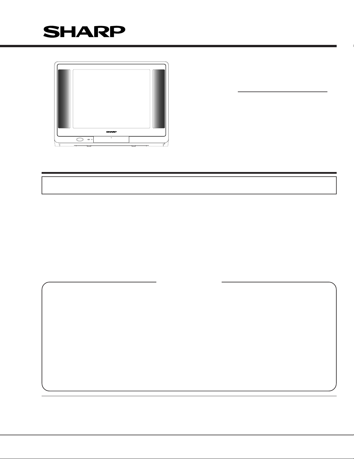
STEREO
21C-FX1(C)/(G)
21C-FX5/FX8
SERVICE MANUAL
S32G721C-FX5/
COLOUR TELEVISION
Chassis No. UAF-C
PUSH OPEN
21C-FX1(C)/(G)
MODELS
In the interests of user-safety (Required by safety regulations in some countries) the set should be restored
to its original condition and only parts identical to those specified should be used.
21C-FX5/FX8
FEATURE
Ë
Multi 21 Systems
Ë
Full Auto Channel Preset and Auto Channel Skip
Ë
100-CH Program Memory
Ë
CATV(Hyper Band) Ready <Used Frequency Synthesizer
Tuner>
Ë
Black Stretch Circuit
Ë
On Timer/Sleep T imer/Reminder Timer
Ë
Blue Back Noise Mute
Ë
Front AV-In & Rear AV-IN/OUT Terminals
Ë
Colour Comb Filter (NTSC Only)
Ë
High Contrast Picture
Ë
Hotel Mode
Ë
Multi Longuages OSD(Eng/Chi/Fre/Malay/Arab/Russian)
Ë
NICAM I, B/G, D/K & A2 STEREO B/G(21C-FX5/FX8)
Ë
TELETEXT (One Page)-English / German / French /
Spanish / Italian / Swedish (21C-FX5)
Ë
White Temperature Adjustment
CONTENTS
Page Page
» SPECIFICATIONS...........................................2
» IMPORTANT SERVICE NOTES...................... 2
» ADJUSTMENT PRECAUTIONS ..................... 3
» HOTEL MODE APPLICATION ...................... 13
» MEMORY MAP..............................................14
» TROUBLE SHOOTING TABLE .....................26
» SOLID STATE DEVICE BASE DIAGRAM.....28
» CHASSIS LAYOUT........................................29
» WAVEFORMS ............................................... 31
» DESCRIPTION OF SCHEMA TIC DIAGRAM..32
» SCHEMATIC DIAGRAM
■ CRT UNIT.................................................33
■ MAIN UNIT ............................................... 34
■ NICAM Unit .............................................. 40
» BLOCK DIAGRAM ........................................42
» PRINTED WIRING BOARD ASSEMBLIES...47
» REPLACEMENT PARTS LIST
■ ELECTRICAL PARTS...............................52
■ MISCELLANEOUS PARTS ......................58
■ SUPPLIED ACCESSORIES.....................58
■ PACKING PARTS.....................................58
■ CABINET PARTS .....................................58
» PACKING OF THE SET ................................ 59
W ARNING
The chassis in this receiver is partially hot. Use an isolation transformer between the line cord plug and power
receptacle, when servicing this chassis. To prevent electric shock, do not remove cover. No user – serviceable
parts inside. Refer servicing to qualified service personnel.
SHARP CORPORATION
1
Page 2

SPECIFICATIONS
Convergence .................................................................Self Convergence System
Focus...................................................................... Quadra-Potential Electrostatic
Sweep Deflection......................................................................................Magnetic
Intermediate Frequencies
Picture IF Carrier .................................................................................. 38.9MHz
Sound IF Carrier Frequency
6.5MHz .............................................................................................. 32.4MHz
6.0MHz .............................................................................................. 32.9MHz
5.5MHz .............................................................................................. 33.4MHz
Colour Sub-Carrier Frequency ...........................................................34.47MHz
Power Input .....................................................................110 ~ 240V AC 50/60 Hz
Power Consumption ......................................................... 111W (21C-FX1(C)/(G))
112W (21C-FX5/FX8)
Audio Power Output Rating ..............................................................7.5W(at Max.)
Speaker
Size............................................................................................ 12 x 6 cm (2pc)
Voice Coil Impedance............................................................. 8 ohms at 400 Hz
Aerial Input Impedance
VHF/UHF .......................................................................... 75 ohms Unbalanced
Receiving System
PAL I, B/G, D/K & SECAM B/G, D/K, -K1 & NTSC M
NICAM B/G & A2 STEREO B/G (21C-FX5/FX8)
Receiving Channel
VHF-Channels .......................................E2(48.25MHz) thru E12(224.25MHz)
C1 (49.75 MHz) thru C12 (216.25 MHz)
S1 (105.25 MHz) thru S41 (463.25 MHz)
UHF-Channels...................................E21(471.25MHz) thru E69(855.25MHz)
C13 (471.25 MHz) thru C57 (863.25 MHz)
Dimensions..................................................................................... Width: 621 mm
Height: 468 mm
Depth: 474 mm
Weight(approx): 25 kg
Cabinet material ....................................................................................All Plastics
Specifications are subject to change without prior notice.
IMPORTANT SERVICE NOTES
Maintenance and repair of this receiver should be done by qualified
service personnel only .
SERVICE OF HIGH VOLTAGE SYSTEM AND PICTURE TUBE
When servicing the high voltage system, remove static charge from it by
Connecting a 10K ohm Resistor in series with an insulated wire(such as a
test probe) between picture tube dag and 2nd anode lead. (AC line cord
should be disconnected from AC outlet.)
1. Picture tube in this receiver employs integral implosion protection.
2. Replace with tube of the same type number for continued safety.
3. Do not lift picture tube by the neck.
4. Handle the picture tube only when wearing shatterproof goggles and after discharging
the high voltage completely.
X-RAY
This receiver is designed so that any X-Ray radiation is kept to an absolute
Minimum. Since certain malfunctions or servicing may produce potentially
hazardous radiation with prolonged exposure at close range, the followin
precautions should be observed:
1. When repairing the circuit, be sure not to increase the high voltage to more than 30.0kV
(at beam 0
µ
A) for the set.
2. To keep the set in a normal opeartion , be sure to make it function on 27.5kV
±
1.5kV (at
beam 1,350
µ
A) in the case of the set. The set has been factory - Adjusted to the above-
mentioned high voltage.
∴∴
∴∴
∴If there is a possibility that the high voltage fluctuates as a result of the repairs,
never forget to check for such high voltage after the work.
3. Do not substitute a picture tube with unauthorizerd types and/or brands which may
cause excess X-ray radiation.
BEFORE RETURNING THE RECEIVER
Before returning the receiver to the user, perform the following safety Checks.
1. Inspect all lead dress to make certain that leads are not pinched or that hardware is not
lodged between the chassis and other metal parts in the receiver.
2. Inspect all protective devices such as non-metallic control knobs, insulating fishpapers,
cabinet backs, adjustment and compartment covers or shields, isolation resistor- capacity networks, mechanical insulators etc.
2
21C-FX1(C)/(G)
21C-FX5/FX8
2-1 2-2
Page 3
ADJUSTMENT PRECAUTIONS
This model’s setting are adjusted in two different ways: through the I
2
C bus control and in the conventional
analog manner. The adjustments via the I
2
C bus control include preset-only items and variable data.
1. Setting the service mode by the microprocessor.
1. Short TP1001 & TP1002 to switch to the service mode position, and the microprocessor is in input
mode. (Adjustment through the I2C bus control).
2. Press the CH DOWN / UP key on the remote controller to get ready to select the mode one by one.
3. Press the CH DOWN / UP key on the remote controller to select the modes reversibly one by one.
4. Using the VOLUME UP/ DOWN key on the remote controller, the data can be modified.
5. Disconnect TP1001 & TP1002 to switch to the normal mode (OFF) position, and the microprocessor
is in out of the service mode.
2. Factory Presetting.
1. Short TP1001 & TP1002 to switch to the service mode position and turn on the main power switch.
Initial values are automatically preset, only when a new EEPROM is used (Judge with the first 4 bytes).
2. The initial data are preset as listed in page 6 & 7.
3. Make sure the data need modify or not (Initial data).
Note: Once the chassis has been assembly together and ready to be POWER ON for the FIRST TIME,
make sure to short TP1001 & TP1002 to switch to the service mode position first and then turn on
the main power switch (See 2-(1) above).
Precaution: If haven’t done this initiation, it may possibly generate excessive Beam current.
3. For reference please check with memory map
(UAF-C Series type RH-IX3410CEN5, RH-IX3412CEN5 Attachment)
4. Trouble indications
If the set is interrupted by IIC bus line error, the following indicators work to identify a spot in trouble.
LED (RED) flashing: Flashing time Part's Ref.No. Remarks
2 IC1003 EEP ROM
3 IC801 TVPROCESSOR
4 IC401 AV SWITCH
5 IC305 SOUND PROCESSOR
6 IC2300 (NICAM/IGR) DECODER
8 TU201 TUNER
SERVICE MODE
(1) In the Service Mode, Key is used to select the mode in the following order.
AGC &
GEOMETRIC
MODE
↓
↓
↓
↓
↓
↓
↓
↓
↓
↓
↓
↓
↓
AGC Take Over Point (AGC)
Vertical Slope (V-LIN)
Vertical Amplitude(V-AMP)
Vertical Shift (V-CENT)
Horizontal shift (H-CENT)
East-West width (H-SIZE)
Horizontal Parallelogram (EW//)
East-west Parabola/Width (PARA)
East-west Upper Corner Parabola (COR(U))
East-west Lower Corner Parabola (COR(L))
East-west Trapezium (TRAPE)
Horizontal Bow (HB)
S-Correction (S-COR)
WHITE POINT
ADJ.
MODE
↓
↓
↓
↓
↓
↓
↓
↓
↓
White point Red Standard white temp.(DRI-RS)
White point Green Standard white temp. (DRI-GS)
White point Blue Standard white temp (DRI-BS)
White point Red Cold white temp. (DRI-RC)
White point Green Cold white temp. (DRI-GC)
White point Blue Cold white temp. (DRI-BC)
White point Red Warm white temp. (DRI-RW)
White point Green Warm white temp. (DRI-GW)
White point Blue Warm white temp. (DRI-BW)
SUB
ADJ.
MODE
↓
↓
↓
↓
↓
↓
↓
↓
↓
↓
↓
↓
↓
Max Volume (SUB-VOL)
Sub Contrast (SUB-CON)
Sub Colour (SUB-COL)
Sub Brightness (SUB-BRI)
Sub Tint (SUB-TINT)
Sub Sharpness (SUB-SHP)
Max Hotel Volume (HTL-VOL)
Hotel Program number (HTL-PRG)
Blue Back Contorast (BB-CON)
OSD RGB Reference (RGB)
Black Level off-set R (CUT-R)
Black Level off-set G (CUT-G)
Cathode Drive Level (CDL)
FORWARD : CH DOWN KEY
REVERSE : CH UP KEY
* ( ) means OSD display.
FORWARD : CH DOWN KEY
REVERSE : CH UP KEY
* ( ) means OSD display.
AGC &
GEOMETRIC
MODE
WHITE POINT
ADJ.
MODE
SUB
ADJ.
MODE
Y-DELAY
ADJ.
MODE
MISC.
OPTION
MODE
IC
OPTION
MODE
OFFSET
ADJ.
MODE
3
3-1 3-2
21C-FX1(C)/(G)
21C-FX5/FX8
Page 4

Bass Mix for AN7396K (BM-ON)
Bass Mix Effect for AN7396K (BM-EFF)
AGC for AN7396 or AN5891 (AGC-ON)
AGC Adjust for AN7396K or AN5891
(AGC-ADJ)
NICAM AGC (AGC-N)
NICAM AGC Gain adjust (GAIN-N)
FM Output Level (FM-LV)
IGR Output Level (IGR-LV)
NICAM Output Level (B/G) (BG-NLY)
NICAM Output Level (I) (I-NLV)
NICAM Output Level (D/K) (DK-NLV)
NICAM lower error limit (LOW-ERR)
NICAM upper error limit (UP-ERR)
IGR Stereo R ch gain adjust
(tda9873) (IGR-STR)
Vertical Scan Disable (VSD)
Black Stretch (BKS)
Automatic Volume Leveling (AVL)
Fast Filter IF-PLL (FFI)
Enable Vertical Guard
(RGB blanking) (EVG)
EHT Tracking mode [HCO] (EHT)
Overscan Switch OFF (OSO)
Auto Colour Limit (ACL)
Forced Colour ON (FCO)
COLOUR OFFSET (PAL) (COL-OP)
COLOUR OFFSET (SECAM) (COL-OS)
COLOUR OFFSET (NTSC358) (COL-O3)
COLOUR OFFSET (NTSC443) (COL-O4)
SHARPNESS OFFSET(PAL) (SHP-OP)
SHARPNESS OFFSET(SECAM) (SHP-OS)
SHARPNESS OFFSET(NTSC358) (SHP-O3)
SHARPNESS OFFSET(NTSC443) (SHP-O4)
Y-DELAY
ADJ.
MODE
↓
↓
↓
↓
↓
↓
↓
↓
↓
↓
Y-Delay time for PAL (TV)
(DL-PT)
Y-Delay time for SECAM (TV)
(DL-ST)
Y-Delay time for N358 (TV)
(DL-3T)
Y-Delay time for N443 (TV)
(DL-4T)
Y-Delay time for B/W (TV)
(DL-TV)
Y-Delay time for PAL (AV)
(DL-PA)
Y-Delay time for SECAM (AV)
(DL-SA)
Y-Delay time for N358 (AV)
(DL-3A)
Y-Delay time for N443 (AV)
(DL-4A)
Y-Delay time for B/W (AV)
(DL-AV)
OFFSET
ADJ.
MODE
↓
↓
↓
↓
↓
↓
↓
↓
IC
OPTION
MODE
↓
↓
↓
↓
↓
↓
↓
↓
↓
↓
↓
↓
↓
↓
↓
↓
↓
↓
↓
↓
↓
↓
↓
Sound system M (S-M)
Sound system DK (S-DK)
Sound system I (S-I)
Sound system BG (S-BG)
Playback SECAM (P-SECAM)
FE (RF) NTSC 3.58 (F-N358)
FE (RF) NTSC 4.43 (F-N443)
FE (RF) SECAM (F-SECAM)
Video Mute at Ident loss (VMI)
Video Mute at program
/source Change (VMC)
Hotel mode (HTL)
Reduced FM demodulator Gain
(for BTSC sig) (BTSC)
Number of external AV sources (AV)
FM Window Selection (FMWS)
Sound Mute bit 0 (SM0)
Sound Mute bit 1 (SM1)
Thai language (THA)
Arabic language (ARA)
Malay language (MAL)
Chinese language (CHI)
French language (FRE)
Russian language (RUS)
A
↓
↓
↓
↓
↓
↓
↓
↓
↓
↓
↓
↓
↓
↓
↓
↓
↓
↓
↓
↓
↓
↓
↓
↓
Forced V-SYNC slicing level (FSL)
Sync of OSD (HP2)
IF AGC speed bit0 (AGC0)
IF AGC speed bit1 (AGC1)
Phi 1 time constant for FE(RF) (FOA-FE)
Phi 2 time constant for FE(RF) (FOB-FE)
Phi 1 time constant for AV (FOA-AV)
Phi 2 time constant for AV (FOB-AV)
Teletext (TXT)
Teletext Western or Eastern characters (TXT-WE)
Teletext pan-European language (TXT-EURO)
IF frequency selection (IF-38.0)
Charge pump (CP)
AN5890 Sound processor present (AN5890)
AN5891 sound processor present (AN5891)
AN7396 sound processor present (AN7396)
NICAM decoding enabled (NICAM)
IGR decoding enabled (IGR)
GAME mode enabled (GAME)
BIL enabled (BIL)
LED Blink Speed When On-Timer is active (LED-F)
PWM Volume table for mono (MSA)
Output Vertical Guard (NDF)
OSD "IGR" or "A2" Display (A2)
MISC.
OPTION
MODE
↓
↓
↓
↓
↓
↓
↓
↓
↓
↓
↓
↓
↓
↓
↓
↓
↓
↓
↓
↓
↓
↓
↓
A
4
4-1 4-2
21C-FX1(C)/(G)
21C-FX5/FX8
Page 5
USER DATA
CONTRAST MAX (64/64)
COLOUR CENT (32/64)
BRIGHTNESS CENT (32/64)
TINT CENT (32/64)
SHARPNESS CENT (32/64)
WHITE TEMP CENT (32/64)
TREBLE CENT (32/64)
BASS CENT (32/64)
SURROUND OFF
BALANCE CENT (32/64)
S-VOLUME MIN (1/64)
BLUE BACK OFF
C SYSTEM AUTO
S SYSTEM *1
USER DATA IN SERVICE MODE
* While SERVICE mode ON, EEPROM DATA will switch to the service data.
Also, once SERVICE mode OFF, EEPROM will switch back to previous USER DATA.
* In the service mode, the user data establish as below,
*1: For each CH, data is
same as before switch
to Service Mode.
* Direct Key-in
MODE KEY-IN KEY
AGC FUNCTION
SUB-BRI BRIGHTNESS UP
DRI-GS TEXT
DRI-BS PICTURE
CUT-R SKIP
CUT-G F2
V-LIN CONTRAST DOWN
V-CENT BRIGHTNESS DOWN
V-AMP COLOUR DOWN
H-CENT TINT DOWN
H-SIZE BALANCE RIGHT
PARA TREBLE UP
TRAPE BASS UP
EW// SHARPNESS DOWN
SUB-COL COLOUR UP
SUB-TINT TINT UP
EEPROM ITEMS OSD DATA LENGTH
INITIAL DATA
FIX/ADJ REMARK
AGC Take Over Point AGC 0 ~ 63 14 (20) ADJ
Vertical Slope V-LIN 0 ~ 63 32 ADJ
Vertical Amplitude V-AMP 0 ~ 63 32 ADJ
Vertical Shift V-CENT 0 ~ 63 32 (15) ADJ
Horizontal shift H-CENT 0 ~ 63 32 ADJ
East-West width H-SIZE 0 ~ 63 32 FIX
Horizontal Parallelogram EW / / 0 ~ 63 32 FIX
East-west Parabola/Width PARA 0 ~ 63 32 FIX
East-west Upper Corner Parabola COR (U) 0 ~ 63 32 FIX
East-west Lower Corner Parabola COR (L) 0 ~ 63 32 FIX
East-west Trapezium TRAPE 0 ~ 63 32 FIX
Horizontal Bow HB 0 ~ 63 32 FIX
S-Correction S-COR 0 ~ 63 0 (24) FIX
White point Red Standard white temp. DRI-RS 0 ~ 63 32 FIX
White point Green Standard white temp. DRI-GS 0 ~ 63 32 ADJ
White point Blue Standard white temp DRI-BS 0 ~ 63 32 ADJ
White point Red Cold white temp. DRI-RC 0 ~ 63 25 FIX *2
White point Green Cold white temp. DRI-GC 0 ~ 63 32 FIX *2
White point Blue Cold white temp. DRI-BC 0 ~ 63 32 FIX (DRI-BS) DATA
White point Red Warm white temp. DRI-RW 0 ~ 63 32 FIX
White point Green Warm white temp. DRI-GW 0 ~ 63 32 FIX (DRI-GS)-7 DATA
White point Blue Warm white temp. DRI-BW 0 ~ 63 32 FIX (DRI-BS)-7 DATA
Max Volume SUB-VOL 0 ~ 60 60 FIX
Sub Contrast SUB-CON 0 ~ 63 63 FIX
Sub Colour SUB-COL 0 ~ 63 32 (20) ADJ
Sub Brightness SUB-BRI 0 ~ 63 32 (20) ADJ
Sub Tint SUB-TINT 0 ~ 63 32 (30) ADJ
Sub Sharpness SUB-SHP 0 ~ 63 32 FIX
Max Hotel Volume HTL-VOL 0 ~ 60 30 FIX
Hotel Program number HTL-PRG
0 ~ 99 OR >99 FOR NONE
255 FIX
Blue Back Contorast BB-CON 0 ~ 15 10 FIX
OSD RGB Reference RGB 0 ~ 15 15 (8) FIX
Black Level off-set R CUT-R 0 ~ 63 32 ADJ
Black Level off-set G CUT-G 0 ~ 63 32 ADJ
Cathode Drive Level CDL 0 ~ 15 0 (9) FIX
Y-Delay time for PAL (TV) DL-PT 0 ~ 15 12 FIX
Y-Delay time for SECAM (TV) DL-ST 0 ~ 15 15 FIX
Y-Delay time for N358 (TV) DL-3T 0 ~ 15 12(5) FIX
Y-Delay time for N443 (TV) DL-4T 0 ~ 15 12(5) FIX
Y-Delay time for B/W (TV) DL-TV 0 ~ 15 12 FIX
Y-Delay time for PAL (AV) DL-PA 0 ~ 15 12 FIX
Y-Delay time for SECAM (AV) DL-SA 0 ~ 15 15 FIX
Y-Delay time for N358 (AV) DL-3A 0 ~ 15 12(5) FIX
Y-Delay time for N443 (AV) DL-4A 0 ~ 15 12(5) FIX
Y-Delay time for B/W (AV) DL-AV 0 ~ 15 12 FIX
After short TP1001 & TP1002, and turn on the MAIN POWER switch, read data from EEPROM address
00H ~ 03H, and compare to the list below, if different, initialize the EEPROM.
Address : Data Address : Data
00H : 55H 02H : 53H
01H : 41H 03H : 36H
5
21C-FX1(C)/(G)
21C-FX5/FX8
5-1 5-2
Page 6
21C-FX1(C)/(G)
EEPROM ITEMS OSD DATA LENGTH
INITIAL DATA
FIX/ADJ REMARK
COLOUR OFFSET (PAL) COL-OP 0 ~ 15 8 FIX *3
COLOUR OFFSET (SECAM) COL-OS 0 ~ 15 8 FIX *3
COLOUR OFFSET (NTSC358) COL-O3 0 ~ 15 4 FIX *3
COLOUR OFFSET (NTSC443) COL-O4 0 ~ 15 4 FIX *3
SHARPNESS OFFSET(PAL) SHP-OP 0 ~ 15 8 FIX
SHARPNESS OFFSET(SECAM) SHP-OS 0 ~ 15 4 FIX
SHARPNESS OFFSET(NTSC358) SHP-O3 0 ~ 15 12 FIX
SHARPNESS OFFSET(NTSC443) SHP-O4 0 ~ 15 8 FIX
Bass Mix for AN7396K BM-ON
0(DISABLE)/1(ENABLE)
0 FIX
Bass Mix Effect for AN7396K BM-EFF 0 ~ 3 2 FIX
AGC for AN7396 or AN5891 AGC-ON
0(DISABLE)/1(ENABLE)
1 FIX
AGC Adjust for AN7396K or AN5891 AGC-ADJ 0 ~ 3 3 FIX
NICAM AGC AGC-N
0(DISABLE)/1(ENABLE)
0 FIX
NICAM AGC Gain adjust GAIN-N 0 ~ 31 0 FIX
FM Output Level FM-LV 0 ~ 30 15 (22) FIX
IGR Output Level IGR-LV 0 ~ 30 16 (23) FIX
NICAM Output Level (B/G) BG-NLV 0 ~ 30 13 (20) FIX
NICAM Output Level (I) I-NLV 0 ~ 30 18 (25) FIX
NICAM Output Level (D/K) DK-NLV 0 ~ 30 13 (20) FIX
NICAM lower error limit LOW-ERR 0 ~ 255 35 FIX
NICAM upper error limit UP-ERR 0 ~ 255 70 FIX
IGR Stereo R ch gain adjust(tda9873) IGR-STR 0 ~ 13 6 FIX
Vertical Scan Disable VSD
0 or 1 (not Stored)
0 FIX
Black Stretch BKS
0(DISABLE)/1(ENABLE)
1 FIX
Automatic Volume Leveling AVL
0(DISABLE)/1(ENABLE)
1 FIX
Fast Filter IF-PLL FFI
0(DISABLE)/1(ENABLE)
0 FIX
Enable Vertical Guard (RGB blanking) EVG
0(DISABLE)/1(ENABLE)
1 FIX
EHT Tracking mode [HCO] EHT
0(DISABLE)/1(ENABLE)
1 FIX
Overscan Switch Off OSO
0(DISABLE)/1(ENABLE)
0 FIX
Auto Colour Limit ACL
0(DISABLE)/1(ENABLE)
0 (1) FIX
Forced Colour ON FCO
0(DISABLE)/1(ENABLE)
0 FIX
Sound system M S-M
0(DISABLE)/1(ENABLE)
*1 FIX
Sound system DK S-DK
0(DISABLE)/1(ENABLE)
*1 FIX
Sound system I S-I
0(DISABLE)/1(ENABLE)
*1 FIX
Sound system BG S-BG
0(DISABLE)/1(ENABLE)
*1 FIX
Playback SECAM P-SECAM
0(DISABLE)/1(ENABLE)
*1 FIX
FE (RF) NTSC 3.58 F-N358
0(DISABLE)/1(ENABLE)
*1 FIX
FE (RF) NTSC 4.43 F-N443
0(DISABLE)/1(ENABLE)
*1 FIX
FE (RF) SECAM F-SECAM
0(DISABLE)/1(ENABLE)
*1 FIX
Video Mute at Ident loss VMI
0(DISABLE)/1(ENABLE)
1 FIX
Video Mute at program/source Change VMC
0(DISABLE)/1(ENABLE)
1 FIX
Hotel mode HTL
0(DISABLE)/1(ENABLE)
0 FIX
Reduced FM demodulator Gain (for BTSC sig) BTSC
0(DISABLE)/1(ENABLE)
0 FIX
Number of external AV sources AV
0 FOR 1 AV / 1 FOR 2 AV
1 FIX
FM Window Selection FMWS
0(DISABLE)/1(ENABLE)
0 FIX
Sound Mute bit 0 SM0
0(DISABLE)/1(ENABLE)
1 FIX
Sound Mute bit 1 SM1
0(DISABLE)/1(ENABLE)
0 FIX
Thai language THA
0(DISABLE)/1(ENABLE)
0 FIX
Arabic language ARA
0(DISABLE)/1(ENABLE)
1 FIX
Malay language MAL
0(DISABLE)/1(ENABLE)
1 FIX
Chinese language CHI
0(DISABLE)/1(ENABLE)
1 FIX
French language FRE
0(DISABLE)/1(ENABLE)
1 FIX
Russian language RUS
0(DISABLE)/1(ENABLE)
1 FIX
EEPROM ITEMS OSD DATA LENGTH
INITIAL DATA
FIX/ADJ REMARK
Forced V-SYNC slicing level FSL
0(DISABLE)/1(ENABLE)
0 FIX
Sync of OSD HP2
0 FOR Ph1 / 1 FOR Ph2
0 FIX
IF AGC speed bit0 AGC0
0(DISABLE)/1(ENABLE)
1 FIX
IF AGC speed bit1 AGC1
0(DISABLE)/1(ENABLE)
0 FIX
Phi 1 time constant for FE(RF) FOA-FE
0(DISABLE)/1(ENABLE)
0 FIX
Phi 2 time constant for FE(RF) FOB-FE
0(DISABLE)/1(ENABLE)
0 FIX
Phi 1 time constant for AV FOA-AV
0(DISABLE)/1(ENABLE)
1 FIX
Phi 2 time constant for AV FOB-AV
0(DISABLE)/1(ENABLE)
1 FIX
Teletext TXT
0(DISABLE)/1(ENABLE)
*1 FIX
Teletext Western or Eastern characters TXT-WE
0(DISABLE)/1(ENABLE)
0 FIX
0 (teletext pan-
Teletext pan-European language TXT-EURO
european language) /
0 FIX
depends on delivery
(Arabic/Russian))
IF frequency selection IF-38.0
0 (IF FREQUENCY 38.9) /
0 FIX
1 (IF FREQUENCY 38.0)
0 (FAST TUNING) /
Charge pump CP
1 (MODERATE
0(1) FIX
SPEED TUNING)
AN5890 Sound processor present AN5890
0(DISABLE)/1(ENABLE)
1(0) FIX
AN5891 sound processor present AN5891
0(DISABLE)/1(ENABLE)
0(1) FIX
AN7396 sound processor present AN7396
0(DISABLE)/1(ENABLE)
0 FIX
NICAM decoding enabled NICAM
0(DISABLE)/1(ENABLE)
*1 FIX
IGR decoding enabled IGR
0(DISABLE)/1(ENABLE)
*1 FIX
GAME mode enabled GAME
0(DISABLE)/1(ENABLE)
0 FIX
BIL enabled BIL
0(DISABLE)/1(ENABLE)
0 FIX
LED blink Speed when On-Timer is active LED-F 0(62.5Hz)/1(1Hz) 0 FIX
PWM volume table for MONO MSA
0(original table)/1(new table)
0 FIX
Output Vertical Guard NDF
0(lgnore)/1(accopl)
0(1) FIX
OSD "IGR" or "A2" display A2
0(display IGR)/1(display A2)
*1 FIX
EEPROM ITEMS OSD DATA LENGTH
FIX/ADJ
*(1) *(2) *(3)
Sound system M S-M
0(DISABLE)/1(ENABLE)
0 (1) 0 (1) 0 (1)
Sound system DK S-DK
0(DISABLE)/1(ENABLE)
111
Sound system I S-I
0(DISABLE)/1(ENABLE)
111
Sound system BG S-BG
0(DISABLE)/1(ENABLE)
111
Playback SECAM P-SECAM
0(DISABLE)/1(ENABLE)
111
FE (RF) NTSC 3.58 F-N358
0(DISABLE)/1(ENABLE)
0 (1) 0 (1) 0 (1)
FE (RF) NTSC 4.43 F-N443
0(DISABLE)/1(ENABLE)
111
FE (RF) SECAM F-SECAM
0(DISABLE)/1(ENABLE)
111
Teletext TXT
0(DISABLE)/1(ENABLE)
0 (1) 0 0
NICAM decoding enabled NICAM
0(DISABLE)/1(ENABLE)
0 (1) 0 (1) 0
IGR decoding enabled IGR
0(DISABLE)/1(ENABLE)
0 (1) 0 (1) 0
OSD "IGR" or "A2" display A2
0(display IGR)/1(display A2)
0 (1) 0 (1) 0
NOTE :
Please set the EEPROM initial data according to the value in parenthesis ( ) before adjustment.
Fixed data, please do not change without specific instruction.
*1: Please refer the following table.
MODEL : *(1) : 21C-FX5 *(2) :21C-FX8 *(3) : 21C-FX1(C)/(G)
*2 :DRI-RC = 27, DRI-GC = (DRI-GS)-5 for 21C-FX1(G)
DRI-RC = 25, DRI-GC = (DRI-GS)-7 for the other models
*3 :After Adjust SUB-COL then change:
1.COL-0P from 8 to 14
2.COL-0S from 8 to 14
3.COL-03 from 4 to 10
4.COL-04 from 4 to 10
21C-FX5/FX8
6
6-1 6-2
Page 7
MCL2
CH-NO Fv (MHz) SOUND SYS
0 590.25 B/G
1 46.25 B/G
2 64.25 B/G
3 86.25 B/G
4 95.25 B/G
5 138.25 B/G
6 175.25 B/G
7 182.25 B/G
8 189.25 B/G
9 196.25 B/G
10 209.25 B/G
11 216.25 B/G
12
13
14
15
16
17
18
19
20
21
22
23
24
25
26
27
28 527.25 B/G
29
30
31
32
33
34
35
36
37 590.25 B/G
38
39
40
41 48.25 B/G
42 62.25 B/G
43 77.25 D/K
44 175.25 B/G
45 183.25 D/K
46 191.25 D/K
47 210.25 B/G
48 224.25 B/G
49 487.25 I
50 503.25 B/G
51 575.25 B/G
52 599.25 B/G
53 621.25 M
54 639.25 D/K
55 735.25 I
56 767.25 B/G
57 815.25 B/G
58 855.25 I
59 91.25 M
60 183.25 M
MCL1
CH-NO Fv (MHz) SOUND SYS
0
1 48.25 B/G
2 62.25 B/G
3 77.25 D/K
4 175.25 B/G
5 182.25 B/G
6 183.25 D/K
7 191.25 D/K
8 196.25 B/G
9 199.25 M
10 210.25 B/G
11 224.25 B/G
12 471.25 B/G
13 487.25 I
14 503.25 B/G
15 575.25 B/G
16 583.25 B/G
17 599.25 B/G
18 621.25 M
19 639.25 D/K
20 703.25 B/G
21 735.25 I
22 767.25 B/G
23 815.25 B/G
24 855.25 I
25 855.25 B/G
26 55.25 M
27 83.25 M
28 183.25 M
29 193.25 M
30 217.25 M
31 471.25 M
32 477.25 M
33 693.25 M
34 885.25 M
35 112.25 B/G
36 168.25 B/G
37
38 294.25 B/G
39 463.25 B/G
40
41 647.25 B/G
42 663.25 B/G
43 679.25 B/G
44 174.95 B/G
45 175.55 B/G
MCL2
CH-NO Fv (MHz) SOUND SYS
61 193.25 M
62 217.25 M
63 471.25 M
64 693.25 M
65 112.25 B/G
66 168.25 B/G
67 294.25 B/G
68 463.25 B/G
69 174.95 B/G
70 175.55 B/G
INITIAL SETTING
In service mode, after execute select POS 1, store the following tuning data in EEPROM.
SHIPPING SETTING & CHECKING
THE FOLLOWING DEFAULT DATA HAS BEEN FACTORY-SET FOR THE EEPROM.
ITEMS DATA SETTING
LAST PROGRAM/CHANNEL 1
FLASHBACK PROGARM/CH 1
DIGIT 2
C-SYSTEM AUTO
S-SYSTEM *1
SKIP OFF
AFC ON
VOLUME 1
CONTRAST 60 (MAX)
COLOUR 0 (CENTER)
BRIGHTNESS 0 (CENTER)
TINT 0 (CENTER)
SHARPNESS 0 (CENTER)
WHITE TEMP STANDARD
TREBLE 0 (CENTER)
BASS 0 (CENTER)
SURROUND OFF
SURROUND LEVEL 0 (CENTER)
BALANCE 0 (CENTER)
REMINDER TIMER
IN-ACTIVE, "--:--"
ON TIMER
IN-ACTIVE, "--:--"
OFF TIMER
IN-ACTIVE, "--:--"
R/C POWER POWER-ON
LANGUAGE *1
BLUE BACK MUTE ON
HOTEL MODE OFF
0 CHANNEL SKIP ON
LAST TV/AV TV
FACTORY SETTING BY MODEL
(Reference: Geomagnetism Adjustment)
*1: Please refer defaults for LANGUAGE and
SOUND SYSTEM per MODEL as follows,
INITIAL DESTINATION LANGUAGE
SOUND
SYSTEM
1 CHINA CHINESE D/K
2 HONGKONG CHINESE I
3 SINGAPORE ENGLISH B/G
4 MIDDLE EAST ARABIC B/G
5 RUSSIA RUSSIAN D/K
6 MALAYSIA MALAY B/G
7 TAHITI FRENCH D/K
8 AUSTRALIA ENGLISH B/G
MODEL MAGNEIC FIELD(V, H) nT BACKGROUND LANG. S-SYS LANG QTY
B 20,000 40,000 12300K CHINESE I 6
C (SINGAPORE) -10,000 40,000 12300K ENGLISH B/G 6
G 30,000 20,000 18000K ARABIC B/G 6
*NOTE FOR OSD TYPE
ENGLISH/CHINESE/FRENCH/ARABIC/MALAY/RUSSIAN
7
7-1 7-2
21C-FX1(C)/(G)
21C-FX5/FX8
Page 8
PIF ADJUSTMENT
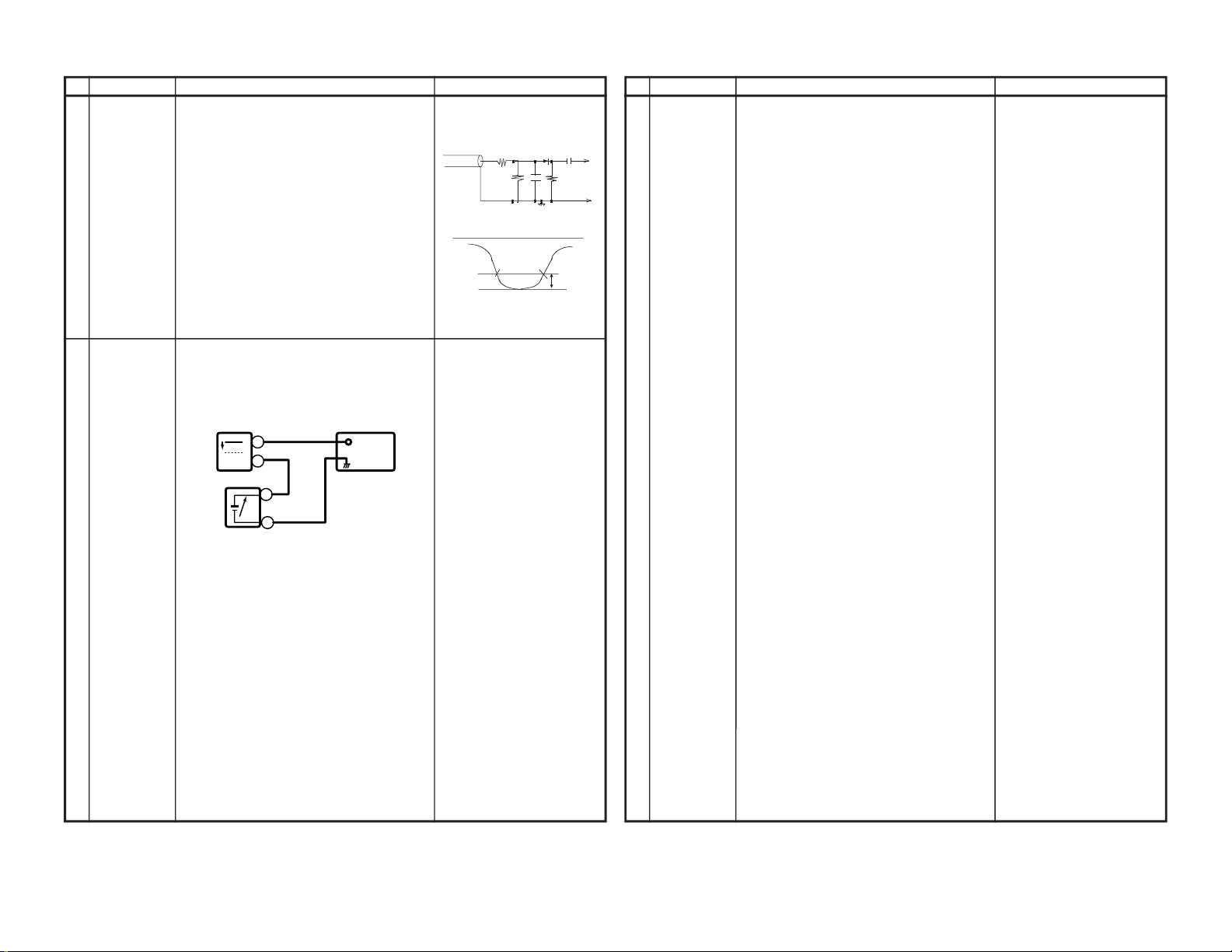
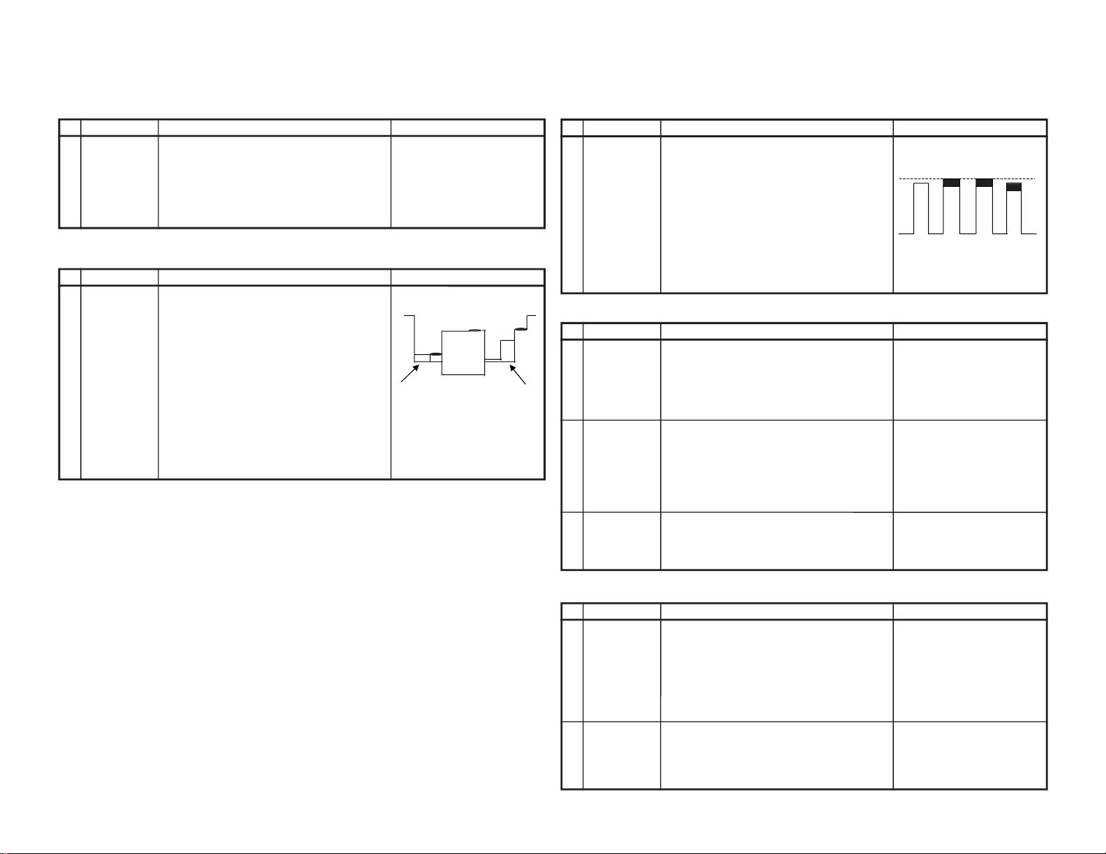
No. Adjusting point Adjusting procedure/conditions Waveform and others
Tuner IFT
( PRESET )
1 1. Get the tuner ready to receive the CH. E - 9
signal,but with no signal input.
Adjust the PLL data.
2. Connect the sweep generator's output cable to
the tuner antenna. ( RF SWEEP )
3. Adjust the sweep generator's to 80dBµV.
4. Connect the response lead ( use LOW IMPEDANCE probe with wave detector ; see Fig.1 ) to
the tuner's IF output terminal. ( This terminal
must have the probe alone connected ).
5. Set the RF AGC to 0 - 6 V with no saturation with
the waveform.
6. Adjust the tuner IF coil to obtain the waveform as
shown in Fig. 2.
Note: Be sure to keep the tuner cover in posi-
tion during this adjustment.
RF-AGC
TAKE OVER
POINT ADJUSTMENT
(I2C BUS
CONTROL)
1. Receive "PAL COLOUR BAR" signal.
» Signal Strength: 54 ± 1 dBµV (75 ohm open)
2. Connect the oscilloscope to TP201 (Tuner’s AGC
Terminal) as shown in Fig. 3.
3. Call "AGC" mode in service mode. Adjust the
"AGC" bus data to obtain the Tuner output pin
drop 0.1V below maximum voltage.
4. Change the antenna input signal to 63~67dBµV,
and make sure there is no noise.
5. Turn up the input signal to 90~95 dBµV to be sure
that there is no cross modulation beat.
Note: For the 50 ohm signal
strength gauge, when not
using 50/75 impedance
adapter, signal strength is
52
±
1dBµV(75 ohm open), in-
stead of 54
±
1dBµV (75 ohm
open).
Precaution: The loss of using
impedance adapter.
2
» Bias box: About 4.5 V
Oscilloscope
0.1V
TV Set
Bias box
TP201+
+
—
—
Fig. 3
E-9 CH
P C
10k
100k
1n60
75ohm
IF OUT
-1.5+/-0.8dB
1000p
1000p
Oscilloscope
Fig.1
Fig.2
SIF (NICAM/IGR) ADJUSTMENT
No. Adjusting point Adjusting procedure/conditions Waveform and others
VCO COIL
T2300
1 1. Receive “PAL colour bar” signal.(E-69)
(Set AFT ON 855.25MHz frequency).
2. Connect DC Voltmater to TP202 (MAIN BOARD
TEST POINT).
3. Check and turn T2300 counter-clockwise (Left)
to 0V and then turn it clockwise (Right) until TP202
become 5V.
After that, turn T2300 counter-clockwise (Left) until
TP202 became 2.5 ± 0.1Vdc.
* UNIT BOARD ADJUSTMENT
Vcc 5V ± 0.1V
IF Input Frequency 38.9MHz ± 0.1V
Adjust T2300 unit TP2300 (NICAM BOARD TEST
POINT) become 2.5 ± 1.0V
Check after assembly NICAM BOARD
Test point: TP202 (IN MAIN BORD).
Preset selected receptiion frequency (AFT OFF)
Check Voltage 2.5 ± 1.0Vdc.
Precaution: The Vcc, fo and other factors are
considered in theunit board of
the 1.0V tolerance which differ
from the adjustment accuracy.
*For model
21C-FX5 and 21C-FX8
8
21C-FX1(C)/(G)
21C-FX5/FX8
8-1 8-2
Page 9
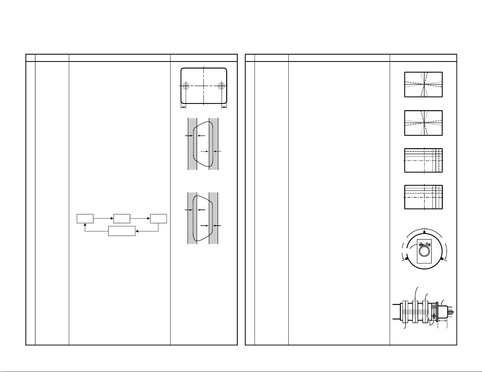
PURITY ADJUSTMENT
No. Adjusting point Adjusting procedure/conditions Waveform and others
PURITY ADJ. 1. Receive the GREEN-ONLY signal. Adjust the
beam current to ~700 µA.
2. Degauss the CRT enough with the degausing coil.
Note: Follow the Job Instruction Sheet to ad-
just the magnetic field.
Vertical Bv: +0.030 mT (0.30 gauss)
Horizontal Bh: +0.020 mT (0.20 gauss)
(Reference: page E-13)
3. Maintain the purity magnet at the zero magnetic
field and keep the static convergence roughly
adjusted.
4. Observe the points a, b as shown in Fig. 4-1
through the microscope. Adjust the landing to the
A rank requirements.
5. Orient the raster rotation to 0 eastward.
6. Tighten up the deflection coil screws.
» Tightening torque: 108 ± 20 N (11 ± 2 kgf)
7. Make sure the CRT corners landing meet the A
rank requirements. If not, stick the magnet sheet
to correct it.
Note: Thi s adjus tment m ust be done after
warming up the unit for 30 minutes or
longer with a beam current over 700
µ
A.
Note: Set the service mode by TP1001 &
TP1002 (short) then press factory process R/C RGB key to change to RGB
mono colour mode.
* For the following colours press R/C RGB key to
change.
1
a
b
A
B
A
30mm 30mm
B
A = B
A = B
Rank "A"
(on the right of the CRT)
Rank "A"
(on the left of the CRT)
Fig. 4-1
Fig. 4-2
Fig. 4-3
* Press R/C RGB key for 1 sec-
ond in NORMAL MODE, the
colour will change to RGB
mono colour mode.
T ext Key “ R.G.Cy “ Key can be
directly use to change to other
colours screen.
Signal-colour
screen cleared
GREEN
ONLY
BLUE
ONLY
RED
ONLY
CONVERGENCE ADJUSTMENT
No. Adjusting point Adjusting procedure/conditions Waveform and others
CONVERGENC
ADJ.
( To be done
after the purity
adjustment.
1. Receive the "Crosshatch Pattern" signal.
2. Using the remote controller, call NORMAL mode.
Static convergence
1. Turn the 4-pole magnet to a proper opening angle in order to superpose the blue and red colours.
2. Turn the 6-pole magnet to a proper opening angle in order to superpose the green colour over
the blue and red colours.
Dynamic convergence
1. Adjust the convergence on the fringes of the
screen in the following steps.
a) Fig. 5-1: Drive the wedge at point "a" and swing
the deflection coil upward.
b) Fig. 5-2: Drive the wedge at points "b" and "c"
and swing the deflection coil downward.
c) Fig. 5-3: Drive the "c" wedge deeper and swing
the deflection coil rightward.
d) Fig. 5-4: Drive the "b" wedge deeper and
swing the deflection coil leftward.
2. Fix all the wedges on the CRT and apply glass
tape over them.
3. Apply lacquer to the deflection yoke lock screw,
magnet unit (purity, 4-pole, 6-pole magnets) and
magnet unit lock screw.
Finally received the Red-only and Blue-only signals to make sure there is no other colours on the
screen.
1
RGB
BGR
R
G
B
R
G
B
B
G
R
B
G
R
RGB
BGR
Lacquer
Wedge "a"
Wedge
"b"
Wedge
"c"
About
100Deg
About
100Deg
4-pole magnet
6-pole magnet
CRT neck
20mm
Lacquer
Purity magnet
Fig. 5-1
Fig. 5-2
Fig. 5-3
Fig. 5-4
Fig. 5-5
Fig. 5-6
9
9-1 9-2
21C-FX1(C)/(G)
21C-FX5/FX8
Page 10
21C-FX1(C)/(G)
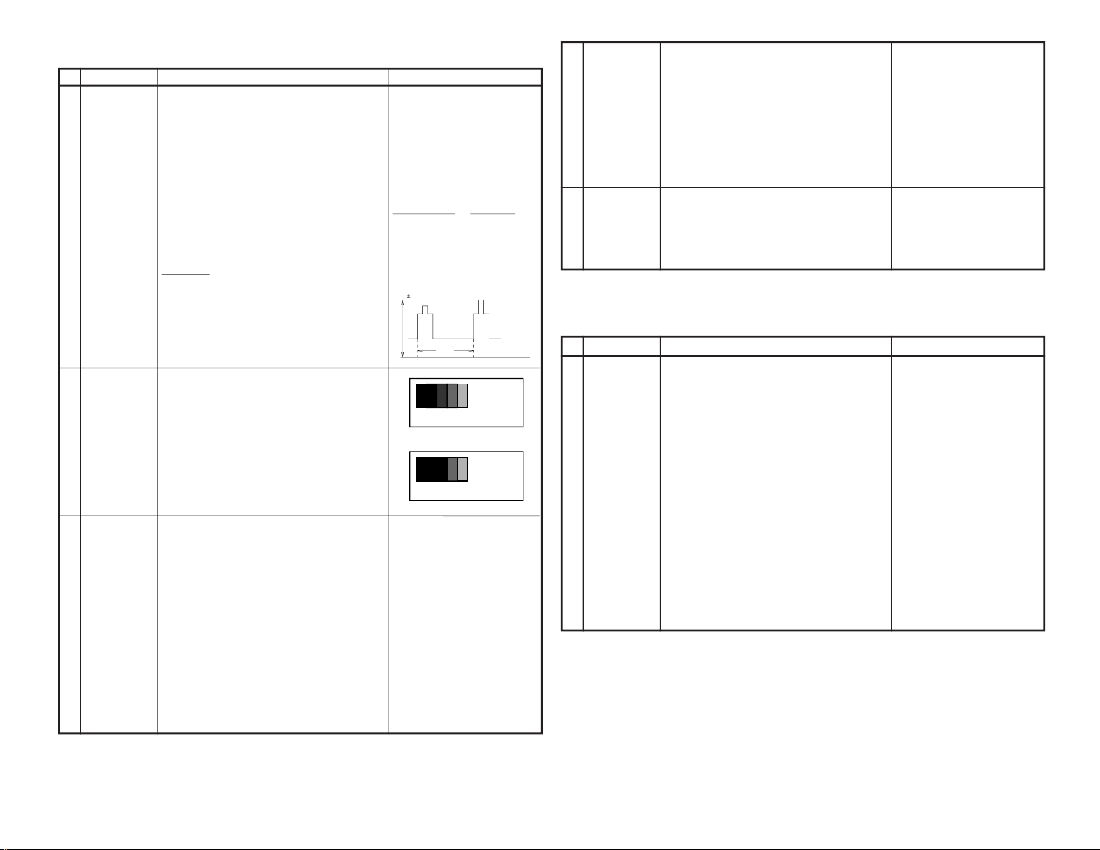
CUT-OFF, BACKGROUND AND SUB-CONTRAST ADJUSTMENT
No. Adjusting point Adjusting procedure/conditions Waveform and others
CRT CUTOFF
ADJUSTMENT
1. Switch TV to VIDEO mode,BLUE BACK OFF, without VIDEO signal.
2. Press R/C to set Picture Normal condition.
3. First off the screen by adjust screen variable resistor.
*4. Next, check AKB circuit function by slowly increase
screen variable resistor until colour raster suddenly
On and Off (AKB start function).
5. Then continue adjust unfil retrace line appear.
6. Finally, slowly decrease the screen variablu resistor unfil screen retrace line (Not Raster) Cut Off.
*NOTE : Must comfirm the AKB function in set before
continue the next adjustment.
REMARK:
1. Before CRT Cutoff adjustment, SUB-BRIGHT, DRIRS/RC/RW, DRI-GS/GC/GW, DRI-BS/BC/BW,
CUT-R and CUT-G must be in initial data.
2. CRT Cutoff adjustment must be done inside a dark
room.
1
20mS
3.2 0.1 Vdc
0
SUB-BRIGHTNESS
ADJUSMENT
(I2C BUS
CONTROL)
1. Call " SUB-BRI" in service mode. (Receive Cross-
hatch pattern with 5 black level windows)
2. Adjust the " SUB BRIGHT " bus data in order that
the line 1 and 2 have the same darkness whereas
line 3 is one step (data) brighter than line 2 .Finally data minus 1 to make line 1,2 and 3 are in
same level darkness.
2
1 2 3 4 5
1
1 2 3 4 5
2
line 3 is one step (data) brighter
than line 2.
WHITE BALANCE SERVICE MODE
ADJ. (I2C BUS
CONTROL)
1. Receive the "WHITE" pattern with BURST SIGNAL.
2. Press R/C to set Picture NORMAL condition.
3. Connect the DC miliammeter between the TP602
(-) TP603 (+).
4. Check Beam current should be around 1,350 µA.
5. Set it to service mode and adjust the " DRI-GS"
(White Point-G), "DRI-BS" (White Point-B) data
to have a colour temperature of 12,300°K or
18000ºK (white).
* Note .
6. Receive "White" pattern, with BURST signal, and
set Brightness Y by generator, to **10cd/m
2
(Minolta CA-100) by reducing Luminate Y signal.
7. Adjust "CUT-R" & "CUT-G" to get 12,300°K or
18000ºK . Then go back normal mode (High
Bright**) to check colour temperature. If out of
range, back to 5.
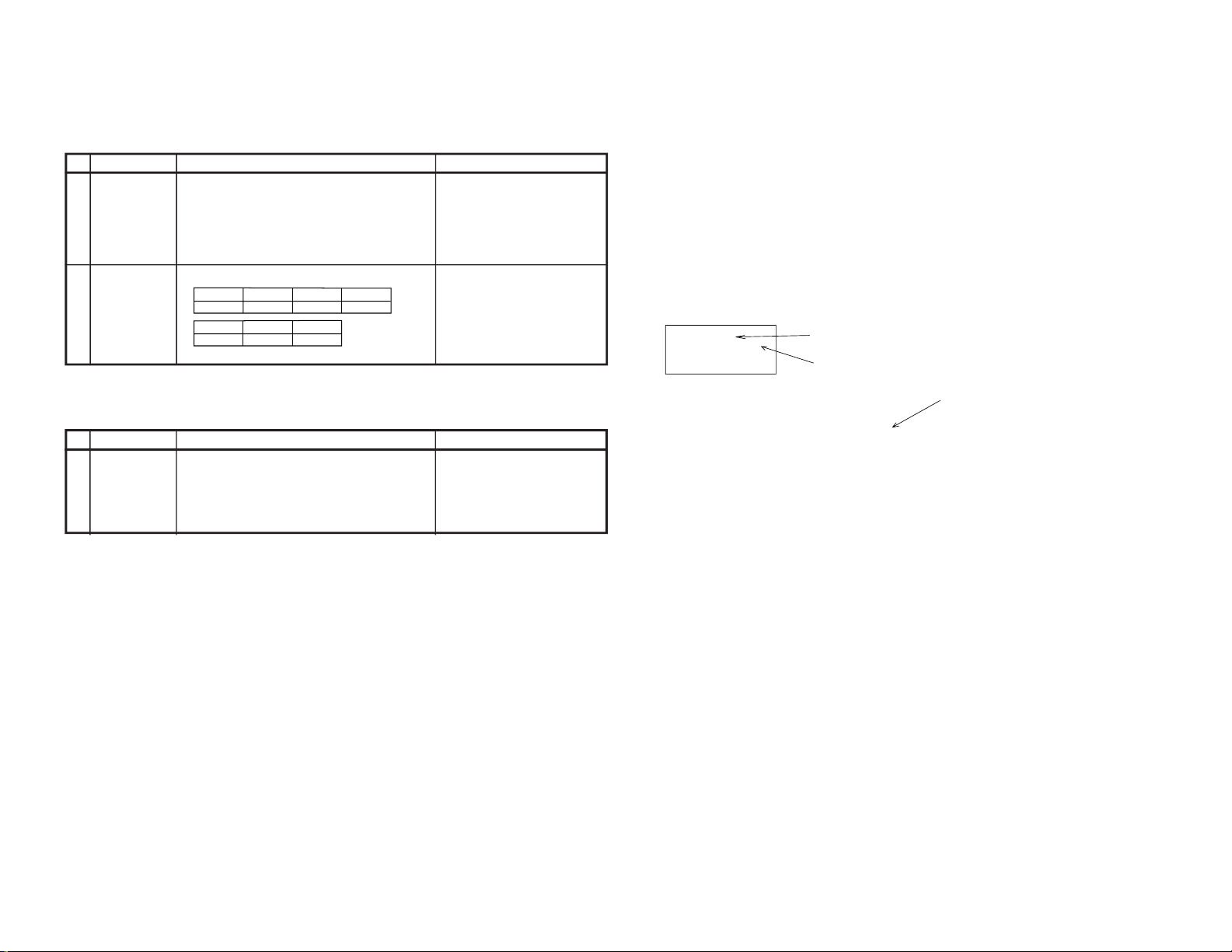
3 Refer to Page 7-2.
*18000°K X: 0.255
Y: 0.255
*12300°K X: 0.272
Y: 0.275
(MINOLTA COLOUR ANALYZER
CA-100)
*Note: Above Data can be UP/
DOWN by Volume key.
Low High
**Note: 10cd/m
2
180cd/m
2
*Alternative Procedure:
(1).Step (1),(2),(3) and (4) are same
as beside procedure.
(2).Then continue adjust until re-
trace appear and make sure the
colour appear wheather red,
green or blue
(3).Connect the oscilloscope to re-
lated test points as below which
is based on colour appear at (2)
Colour Appear Test Point
RED TP 851
GREEN TP 852
BLUE TP 853
(4).Then adjust SCREEN VR until
the tip of signal reach
3.2Vdc±0.1Vdc
HORIZONTAL AND VERTICAL DEFLECTION LOOP ADJUSTMENT
No. Adjusting point Adjusting procedure/conditions Waveform and others
V-LINEARITY
(I2C BUS
CONTROL)
V-CENTER
(I2C BUS
CONTROL)
V - AMP (I2C
BUS CONTROL)
H-CENTER
(I2C BUS
CONTROL)
S-CORRECTION
1. Receive Monoscope Pattern Signal.
2. Call the "V-LIN" mode.
3. Increase or decrease "V-LIN" by Volume key till
the horizontal line in the center of monoscope is
just at the position where the blanking starts.
1. Call the "V-CENT" mode.
2. Increase or decrease "V-CENT" by Volume key
till the picture is centered.
1. Call the "V-AMP" mode.
2. Increase or decrease "V - AMP" by Volume key
to set overscan of 8.5% typical.
Adjustment Spec 8.5% range +1% -1%.
1. Call the "H-CENT" mode.
2. Increase or decrease "H-CENT" by Volume key
to center the picture horizontal.
24(FIX DATA)
1
2
3
4
5
Maximum
beam check
1. Receive the "Monoscope Pattern" signal.
2. Press R/C to set Picture NORMAL condition.
3. Connect the DC miliammeter between TP603 (+)
and TP602 (–).
(Full Scale: 3 mA Range)
4. Beam current must be within 1,350 ± 100 µA.
4
Note: This ad justment must be done after
warming up the unit for 30 minutes or
longer with a beam current over 700
µ
A).
* ADJUST DRI-GC/GW, DRI-BC/BW AS FOLLOW-
ING DAT A, AFTER FINISHING DRI-GS AND DRIBS. *(12300ºK)
DRI-GC/GW DATA = “DRI-GS”-7 DATA
DRI-RC = 25; DRI-BC = DRI-BS; DRI-RW = 32
DRI-BW DATA = “DRI-BS”-7 DATA
*18000ºK
DRI-GW = "DRI-GS" DATA -7
DRI-BW = "DRI-BS" DATA -7
DRI-GC = "DRI-GS" DATA-5
DRI-RC = 27
21C-FX5/FX8
10
10-1 10-2
Page 11
FOCUS ADJUSTMENT
No. Adjusting point Adjusting procedure/conditions Waveform and others
Focus 1. Receive the “Monoscope Pattern” signal.
2. Press R/C to set Picture NORMAL condition.
3. Adjust the focus control to get the best focusing.
1
PAL CHROMA ADJUSTMENT
No. Adjusting point Adjusting procedure/conditions Waveform and others
SUB COLOUR
(I2C BUS
CONTROL)
1. Receive the “PAL Color Bar” signal.
2. Press R/C to set Picture Normal condition.
3. Connect the oscilloscope to Red cathode.
Range : 20 V/Div (AC)
(Using 10:1 Probe)
Sweep Time : 10 µ sec/Div
4. Using the R/C call “SUB-COL” in SERVICE mode.
Adjust SUB COLOUR bus data, so that the 75%
White & Red portions of PAL Color Bar be at the
same level shown as Fig 10.
5. Clear the SERVICE mode.
* Before Adjust SUB-COL, COL-0P=8, COL-0S=8,
COL-03=4, COL-04=4.
After Adjust SUB-COL, set COL-0P=14, COL0S=14, COL-03=10, COL-04=10
1
Fig. 10
Cy G B
W Y 100% W Mg R
75%
No. Adjusting point Adjusting procedure/conditions Waveform and others
SUB-TINT (I2C
BUS CONTROL)
1. Receive the "NTSC3.58 Colour Bar" signal
through AV in.
2. Connect the oscilloscope to TP853 (Pin (5) of
P882) BLUE-OUT.
» Range : 100 mV/Div. (AC)(Use Probe 10:1)
» Sweep time : 10 µsec/Div.
3. Call the "SUB-TINT" mode in service mode. Adjust the "SUB-TINT" bus data to obtain the waveform shown as Fig. 11.
4. Clear the SERVICE mode.
1
Fig. 11
NTSC CHROMA ADJUSTMENT
No. Adjusting point Adjusting procedure/conditions Waveform and others
BEAM PROTECTOR
1. Receive "Monoscope Pattern" signal.
2. Set CONTRAST MAX.
3. Set BRIGHT MAX.
4. During the Collector & Emitter of Q883/5/7 short,
make sure the protector ON and switch to standby
mode.
1 * Select one of Q883/5/7 to do
each short test.
H, V PROTECTOR
1. Receive "Monoscope Pattern" signal.
2. Connect output of Bias Box to D607 cathode
(R606 side).
3. Set voltage of Bias Box to 18V and make sure
the protector is not work.
4. Set voltage of Bias Box to 27V, and make sure
the protector is work.
2
OTHER PROTECTOR
1. Once finish rectified Electrolytic Capacitor short
testing in +B line, check all possible damaged
components on +B line.
(Use random selected set for inspection)
3
PROTECTOR OPERATION CHECKING
No. Adjusting point Adjusting procedure/conditions Waveform and others
VIDEO AND
AUDIO
OUTPUT
CHECK
1. Receive the "PAL Color Bar" signal (100% White
Color Bar, Sound 400 Hz 100% Mod.)
2. Terminate the Video output with a 75 ohm impedance. Make sure the output is as specified (1.0
Vp-p ±3 dB).
3. Terminate the Audio output with a 10k ohm impedance. Make sure the output is as specified
(1.76 Vp-p ±3 dB).
1
VIDEO AND
AUDIO INPUT
CHECK
1. Using the TV/AV key on the remote controller,
make sure that the modes change in order of TV ,
AV1, AV2 & TV again and the video & audio output are according to the input terminal for each
mode.
2
A/V INPUT AND OUTPUT CHECKING
SAME LEVEL
W Y Cy G Mg R B
11
11-1 11-2
21C-FX1(C)/(G)
21C-FX5/FX8
Page 12
FUNCTION OPERATION CHECKING (VIDEO AND AUDIO)
No. Adjusting point Adjusting procedure/conditions Waveform and others
CONTRAST
key
1. Receive "Monoscope Pattern" signal.
2. Set P-Mode to select CONTRAST.
3. Press Volume Up/Down key to check whether the
CONTRAST effect is OK or not.
1
1. Receive "Color Bar" signal.
2. Set P-Mode to select COLOUR.
3. Press Volume Up/Down key to check whether
the COLOUR effect is OK or not.
2
COLOUR key
BRIGHTNESS
key
1. Receive "Monoscope Pattern" signal.
2. Set P-Mode to select BRIGHTNESS.
3. Press Volume Up/Down key to check whether
the BRIGHTNESS effect is OK or not.
3
TINT key 1. Receive the "NTSC Colour Bar" signal thru AV in.
2. Set P-Mode to select TINT.
3. Press Volume Up/Down key to check TINT, UP
for GREEN direction and DOWN for PURPLE direction whether is OK or not.
4
SHARPNESS
Key
1. Receive "Monoscope Pattern" signal.
2. Set P-mode to select SHARPNESS.
3. Press Volume Up/Down key to check whether
the SHARPNESS effect is OK or not.
5
White Temp 1. Receive "Monoscope Pattern" signal.
2. Set FUNCTION to select WHITE TEMP.
3. Press Volume Up/Down key to check WHITE
TEMP Option, STANDARD:
NORMAL SETTING, WARM for more REDDISH
direction changing, COOL for more BLUISH direction changing.
8
NORMAL Key7
1. Once in PICTURE Mode, and the NORMAL key
is pressed, all the settings will be present to normal setting.
(Normal setting value for every mode).
» CONTRAST : MAX
» COLOUR : CENTER
» BRIGHTNESS : CENTER
» TINT : CENTER
» SHARPNESS : CENTER
Notes:If nothing is display
mean contrast, colour, bright,
tint, sharpness are all in normal setting.
CH DISPLAY
COLOUR
1. All Ch (1~99) will have an OSD display of the
channel number in green colour under AFT ON
condition.
6
FUNCTION OPERATION CHECKING (VIDEO AND AUDIO)
(Continued)
No. Adjusting point Adjusting procedure/conditions Waveform and others
Colour
system
1. Receive the "PAL COLOUR BAR" signal, press
the COLOUR SYSTEM key to select modes except PAL, check the COLOUR is not working properly. Then, select the "PAL" mode. Check again
its colour so that it is working properly.
2. Receive "SECAM COLOUR BAR" signal, press
COLOUR SYSTEM key to select modes except
SECAM, check the COLOUR is not working properly. Then, select the "SECAM" mode. Check
again its colour so that it is working properly.
3. Receive “NTSC 4.43/3.58 COLOUR BAR” signal
thru AV, press COLOUR SYSTEM key to select
modes except N4.43/3.58, check the COLOUR
is not working properly. Then, select the “NTSC
4.43/3.58” mode. Check again its colour so that it
is working properly.
12
Sound
system
13
1. Receive “PAL-D/K” signal, press the “SOUND
SYSTEM” to select B/G, I. Check the sound output is not working properly. Select D/K and check
the sound output to make sure it is working properly.
2. Receive “PAL-I” signal, press the “SOUND SYSTEM” to select B/G, D/K. Check the sound output
is not working properly. Select I and check the
sound output to make sure it is working properly.
3. Receive “PAL-B/G” signal, press the “SOUND
SYSTEM” to select I, D/K. Check the sound output is not working properly. Select B/G and check
the sound output to make sure it is working properly.
4. Receive “NTSC-M” signal thru AV, press the
“SOUND SYSTEM” to select B/G, D/K, I, check
the sound output is not working properly. Select
M and check the sound output to make sure it is
working properly.
TREBLE 1. Receive “Monoscope Pattern” signal.
2. Set FUNCTION to select TREBLE.
3. Press Volume Up/Down key to check whether
the TREBLE effect is OK or not.
9
BASS 1. Receive “Monoscope Pattern” signal.
2. Set FUNCTION to select BASS.
3. Press Volume Up/Down key to check whether
the BASS effect is OK or not.
10
BALANCE 1. Receive “Monoscope Pattern” signal.
2. Set FUNCTION to select BALANCE.
3. Press Volume Up/Down key to check whether
the Left-to-Right BALANCE effect is OK or not.
11
12
12-1 12-2
21C-FX1(C)/(G)
21C-FX5/FX8
Page 13
HEADPHONE JACK CHECKING
No. Adjusting point Adjusting procedure/conditions Waveform and others
HEADPHONE
OUTPUT
CHECKING
1. Receive PAL COLOUR P AR with SOUND 400Hz,
100% MODULATION (±50kHz Dev).
2. Maximum volume, and check the headphone
output with 400Hz sound and no sound out from
speaker.
1
FUNCTION OPERATION CHECKING (VIDEO AND AUDIO)
(Continued)
No. Adjusting point Adjusting procedure/conditions Waveform and others
NOISE MUTE
CHECKING
1. Receive "PAL COLOUR BAR" signal.
2. Turn up the volume control to maximum, make
sure the sound is heard from the speakers. Then
put the unit in no signal state.
3. Check the sound mute is effective.
4. Finally turn sound level of CTV to minimum.
14
OSD LANGUAGE
QUANTITY
CHECK
Check OSD LANGUAGE quantity and type15
QUANTITY6ENGLISH
O
CHINESEOMALAY
O
FRENCHOARABIC
O
RUSSIAN
O
HOTEL MODE APPLICATION
How to enable/disable the "Hotel Mode" ?
Ans: a) Press the Menu key.
b) Using the CH UP or CH DW key, move the cursor to FEATURE. Press the VL UP or VL DW key.
c) Using the CH UP or CH DW key, move the cursor to BLUE BACK on the menu screen.
d) Hold down the digit key (-/--) of the remote control for 5 seconds or more, and the Hotel Mode will be made
active.
e) Key in the four digits password starting with number "1", "3", "7", "9", then the hotel mode will be enable,
you can switch on/off the hotel mode by using R/C (volume up/down) key.
* We recommend
Before set the hotel mode, it is better to choose ch 1 & set s-vol level Up to 75% full scale.
After set hotel mode, starting channel will be always ch 1 & maximum sound level out will be set the half of
full scale. (Note: If the sound volume is set to any level below 30, the setting is taken as maximum.)
* If you set hotel mode in AV, starting channel will be the last ch which you received before power off (same as
normal operation)
HOTEL ON
PASSWORD ****
Set vol up/down by R/C key.
Input 1,3,7 and 9 by R/C key.
#1Ch 1 is your selected channel
for hotel mode.
CONDITION:
When using hotel mode, user can control "contrast", "brightness", "sharpness" and "tint" function.
But after power off, it will return to the initial setting.
You can't use:--
Preset mode
Fine tuning
Skip mode
System selection
The others function is allowed to be used.
13
13-1 13-2
21C-FX1(C)/(G)
21C-FX5/FX8
Page 14
21C-FX1(C)/(G)
21C-FX5/FX8
MEMORY MAP
ADDRESS
(HEX)
00
01
02
03
04
05
06
07
08
09
0A
0B
0C
0D
0E
0F
10
11
12
13
14
15
16
17
18
19
1A
1B
1C
1D
1E
1F
20
21
22
23
24
25
26
27
28
29
2A
2B
2C
2D
2E
2F
30
31
32
33
34
35
36
37
38
39
3A
3B
3C
3D
3E
3F
D7 D6 D5 D4 D3 D2 D1 D0
DATA
PASS WORD
PASS WORD
PASS WORD
PASS WORD
AGC TAKE-OVER
V-SLOPE
V-AMPLITUDE
V-CENTER
H-CENTER
H-SIZE
EW-PARALLELOGRAM
EW-PARABOLA/WIDTH
EW-UPPER CORNER
EW-LOWER CORNER
EW-TRAPEZIUM
HORIZONTAL-BOW
S-CORRECTION
DRIVE-R (STANDARD)
DRIVE-G (STANDARD)
DRIVE-B (STANDARD)
DRIVE-R (WARM)
DRIVE-G (WARM)
DRIVE-B (WARM)
DRIVE-R (COOL)
DRIVE-G (COOL)
DRIVE-B (COOL)
SUB-VOLUME
SUB-CONTRAST
SUB-COLOUR
SUB-BRIGHTNESS
SUB-TINT
SUB-SHARPNESS
HTL-VOLUME
HTL-PROGRAM NUMBER
BLUE BACK CONTRAST
OSD-REFERENCE
CUTOFF LEVEL -OFFSET R
CUTOFF LEVEL -OFFSET G
CATHODE DRIVE LEVEL
Y-DELAY (TV PAL)
Y-DELAY (TV SECAM)
Y-DELAY (TV N358)
Y-DELAY (TV N443)
Y-DELAY (TV BW)
Y-DELAY (AV PAL)
Y-DELAY (AV SECAM)
Y-DELAY (AV N358)
Y-DELAY (AV N443)
Y-DELAY (AV BW)
COLOUR-OFFSET (PAL)
COLOUR-OFFSET (SECAM)
COLOUR-OFFSET (N358)
COLOUR-OFFSET (N443)
SHARPNESS-OFFSET (PAL)
MODEL
MICON EEPROM EEPROM CHASSIS CTV FINAL LAST INITIAL
DEFAULT RANGE WRITE(CPU) CHECK DATA CHECK TYPE CHECK DATA CHECK TYPE SETTING DATA REMARK
55 00-FF
41 00-FF
53 00-FF
36 00-FF
0E 00-3F
20 00-3F
20 00-3F
20 00-3F
20 00-3F
20 00-3F
20 00-3F
20 00-3F
20 00-3F
20 00-3F
20 00-3F
20 00-3F
00 00-3F
20 00-3F
20 00-3F
20 00-3F
20 00-3F
20 00-3F
20 00-3F
19 00-3F
20 00-3F
20 00-3F
3C 00-3C
3F 00-3F
20 00-3F
20 00-3F
20 00-3F
20 00-3F
1E 00-3C
FF 00-FF
0A 0-0F
0F 00-0F
20 00-3F
20 00-3F
00 00-0F
0C 00-0F
0F 00-0F
0C 00-0F
0C 00-0F
0C 00-0F
0C 00-0F
0F 00-0F
0C 00-0F
0C 00-0F
0C 00-0F
08 00-0F
08 00-0F
04 00-0F
04 00-0F
08 00-0F
MODEL
LETTER NO.
LETTER NO.
14
Page 15

MEMORY MAP
ADDRESS
40
41
42
43
44
45
46
47
48
49
4A
4B
4C
4D
4E
4F
50
51
52
53
54
55
56
57
58
59
5A
5B
5C
5D
5E
5F
60
61
62
63
64
65
66
67
68
69
6A
6B
6C
6D
6E
6F
70
71
72
73
74
75
76
77
78
79
7A
7B
7C
7D
7E
7F
DATA MICON EEPROM EEPROM CHASSIS CTV FINAL LAST INITIAL
(HEX) D7 D6 D5 D4 D3 D2 D1 D0 DEFAULT RANGE WRITE(CPU) CHECK DATA CHECK TYPE CHECK DATA CHECK TYPE SETTING DATA REMARK
SHARPNESS-OFFSET (SECAM) 04 00-0F
SHARPNESS-OFFSET (N358) 0C 00-0F
SHARPNESS-OFFSET (N443) 08 00-0F
BM-ON 00 00-01
BM-EFFECT 02 00-0F
AGC-ON 01 00-01
AGC ADJUST 03 00-0F
AGC-N 00 00-01
GAIN-N 00 00-1F
FM OUTPUT LEVEL 0F 00-1E
IGR OUTPUT LEVEL 10 00-1E
NICAM OUTPUT LEVEL (B/G) 0D 00-1E
NICAM OUTPUT LEVEL (I) 12 00-1E
NICAM OUTPUT LEVEL (D/K) 0D 00-1E
NICAM LOWER ERROR LIMIT 23 00-FF
NICAM UPPER ERROR LIMIT 46 00-FF
IGR STEREO R CH GAIN ADJ. 06 00-0F
OP_BKS 1B 00-FF
OP_S_M DE 00-FF
OP_VMI 53 00-FF
OP_THA 3E 00-FF
OP_AGC0 31 00-FF
OP_TXT_EU 08 00-FF
OP_GAME 00 00-3F
OP_FCO OP_ACL OP_OSO OP_EHT OP_EVG OP_FFI OP_AVL
OP_FSECAM OP_FN443 OP_F358 OP_PSECAM OP_S_BG OP_S_I OP_S_DK
OP_SM1 OP_SM0 OP_FMWS OP_AV OP_BTSC OP_HTL OP_VMC
OP_HP2 OP_FSL OP_RUS OP_FRE OP_CHI OP_MAL OP_ARA
OP_TXT_WE OP_TXT OP_FOB_AV OP_FOA_AV OP_FOB_FE OP_FOA_FE OP_AGC1
OP_IGR OP_NICAM OP_AN739 6 OP_AN589 1 OP_AN589 0 OP_CP OP_IF38_0
OP_A2 OP_NDF OP_MSA OP_LED_F OP_BIL
LAST VOLUME
01 00-3C
LAST BALANCE 1E 00-3C
LAST BASS 1E 00-3C
LAST TREBLE 1E 00-3C
LAST SURR ON/OFF 00 00-02
LAST SURROUND LEVEL 1E 00-3C
LAST SPAT ON/OFF 00 00-02
LAST SPATIALIZER LEVEL 1E 00-3C
LAST CONTRAST 3C 00-3C
LAST COLOUR 1E 00-3C
LAST BRIGHTNESS 1E 00-3C
LAST TINT 1E 00-3C
LAST SHARPNESS 1E 00-3C
LAST WHITE_TEMP 00 00-02
LAST BALANCE-G 1E 00-3C
LAST BASS-G 1E 00-3C
LAST TREBLE-G 1E 00-3C
LAST SURR ON/OFF-G 00 00-02
LAST SURROUND LEVEL-G 1E 00-3C
LAST SPAT ON/OFF-G 00 00-02
LAST SPATIALIZER LEVEL-G 1E 00-3C
LAST CONTRAST-G 3C 00-3C
LAST COLOUR-G 1E 00-3C
LAST BRIGHTNESS-G 1E 00-3C
LAST TINT-G 1E 00-3C
LAST SHARPNESS-G 1E 00-3C
LAST WHITE_TEMP-G 00 00-02
LAST PROGRAM/SOURCE 01 00-FF
MODEL MODEL
LETTER NO. LETTER NO.
(Continued)
21C-FX1(C)/(G)
21C-FX5/FX8
15
Page 16

21C-FX1(C)/(G)
21C-FX5/FX8
MEMORY MAP
(Continued)
ADDRESS
(HEX) D7 D6 D5 D4 D3 D2 D1 D0
80
81
82
83
DATA
FAVOURITE PROGRAM RED
FAVOURITE PROGRAM GREEN
FAVOURITE PROGRAM YELLOW
FAVOURITE PROGRAM CYAN
84
85
86
87
88
89
DIGIT
LANGUAGE
POWER
B_BACK
8A
8B
8C
8D
8E
8F
90
ON TIMER
OFF TIMER
REMINDER
FADE IN VOLUME
TMR_FLAG
91
92
SKIP 0 SKIP 1 SKIP 2 SKIP 3 SKIP 4 SKIP 5 SKIP 6 SKIP 7
93
SKIP 8 SKIP 9 SKIP 10 SKIP 11 SKIP 12 SKIP 13 SKIP 14 SKIP 15
94
SKIP 16 SKIP 17 SKIP 18 SKIP 19 SKIP 20 SKIP 21 SKIP 22 SKIP 23
95
96
SKIP 24 SKIP 25 SKIP 26 SKIP 27 SKIP 28 SKIP 29 SKIP 30 SKIP 31
SKIP 32 SKIP 33 SKIP 34 SKIP 35 SKIP 36 SKIP 37 SKIP 38 SKIP 39
97
98
SKIP 40 SKIP 41 SKIP 42 SKIP 43 SKIP 44 SKIP 45 SKIP 46 SKIP 47
SKIP 48 SKIP 49 SKIP 50 SKIP 51 SKIP 52 SKIP 53 SKIP 54 SKIP 55
99
SKIP 56 SKIP 57 SKIP 58 SKIP 59 SKIP 60 SKIP 61 SKIP 62 SKIP 63
9A
9B
SKIP 64 SKIP 65 SKIP 66 SKIP 67 SKIP 68 SKIP 69 SKIP 70 SKIP 71
SKIP 72 SKIP 73 SKIP 74 SKIP 75 SKIP 76 SKIP 77 SKIP 78 SKIP 79
9C
9D
SKIP 80 SKIP 81 SKIP 82 SKIP 83 SKIP 84 SKIP 85 SKIP 86 SKIP 87
SKIP 88 SKIP 89 SKIP 90 SKIP 91 SKIP 92 SKIP 93 SKIP 94 SKIP 95
9E
9F
SKIP 96 SKIP 97 SKIP 98 SKIP 99
A0
A1
IGR 0 IGR 1 IGR 2 IGR 3 IGR 4 IGR 5 IGR 6 IGR 7
A2
IGR 8 IGR 9 IGR 10 IGR 11 IGR 12 IGR 13 IGR 14 IGR 15
A3
A4
IGR 16 IGR 17 IGR 18 IGR 19 IGR 20 IGR 21 IGR 22 IGR 23
IGR 24 IGR 25 IGR 26 IGR 27 IGR 28 IGR 29 IGR 30 IGR 31
A5
A6
IGR 32 IGR 33 IGR 34 IGR 35 IGR 36 IGR 37 IGR 38 IGR 39
IGR 40 IGR 41 IGR 42 IGR 43 IGR 44 IGR 45 IGR 46 IGR 47
A7
IGR 48 IGR 49 IGR 50 IGR 51 IGR 52 IGR 53 IGR 54 IGR 55
A8
A9
IGR 56 IGR 57 IGR 58 IGR 59 IGR 60 IGR 61 IGR 62 IGR 63
IGR 64 IGR 65 IGR 66 IGR 67 IGR 68 IGR 69 IGR 70 IGR 71
AA
IGR 72 IGR 73 IGR 74 IGR 75 IGR 76 IGR 77 IGR 78 IGR 79
AB
IGR 80 IGR 81 IGR 82 IGR 83 IGR 84 IGR 85 IGR 86 IGR 87
AC
AD
IGR 88 IGR 89 IGR 90 IGR 91 IGR 92 IGR 93 IGR 94 IGR 95
IGR 96 IGR 97 IGR 98 IGR 99
AE
AF
B0
B1
NICAM 0 NICAM 1 NICAM 2 NICAM 3 NICAM 4 NICAM 5 NICAM 6 NICAM 7
NICAM 8 NICAM 9 NICAM 10 NICAM 11 NICAM 12 NICAM 13 NICAM 14 NICAM 15
B2
NICAM 16 NICAM 17 NICAM 18 NICAM 19 NICAM 20 NICAM 21 NICAM 22 NICAM 23
B3
B4
NICAM 24 NICAM 25 NICAM 26 NICAM 27 NICAM 28 NICAM 29 NICAM 30 NICAM 31
NICAM 32 NICAM 33 NICAM 34 NICAM 35 NICAM 36 NICAM 37 NICAM 38 NICAM 39
B5
B6
NICAM 40 NICAM 41 NICAM 42 NICAM 43 NICAM 44 NICAM 45 NICAM 46 NICAM 47
NICAM 48 NICAM 49 NICAM 50 NICAM 51 NICAM 52 NICAM 53 NICAM 54 NICAM 55
B7
B8
NICAM 56 NICAM 57 NICAM 58 NICAM 59 NICAM 60 NICAM 61 NICAM 62 NICAM 63
NICAM 64 NICAM 65 NICAM 66 NICAM 67 NICAM 68 NICAM 69 NICAM 70 NICAM 71
B9
NICAM 72 NICAM 73 NICAM 74 NICAM 75 NICAM 76 NICAM 77 NICAM 78 NICAM 79
BA
BB
NICAM 80 NICAM 81 NICAM 82 NICAM 83 NICAM 84 NICAM 85 NICAM 86 NICAM 87
NICAM 88 NICAM 89 NICAM 90 NICAM 91 NICAM 92 NICAM 93 NICAM 94 NICAM 95
BC
BD
NICAM 96 NICAM 97 NICAM 98 NICAM 99
BE
BF
MODEL MODEL
MICON EEPROM EEPROM CHASSIS CTV FINAL
DEFAULT RANGE
WRITE(CPU) CHECK DATA CHECK TYPE CHECK DATA CHECK TYPE SETTING DATA
0A 00-FF
14 00-FF
1E 00-FF
28 00-FF
01 00-01
00 00-01
00 00-06
80 00-01
00 00-4D
00 00-4D
00 00-4D
FF 00-FF
00 00-01
80 00-FF
00 00-FF
00 00-FF
00 00-FF
00 00-FF
00 00-FF
00 00-FF
00 00-FF
00 00-FF
00 00-FF
00 00-FF
00 00-FF
00 00-FF
FF 00-FF
FF 00-FF
FF 00-FF
FF 00-FF
FF 00-FF
FF 00-FF
FF 00-FF
FF 00-FF
FF 00-FF
FF 00-FF
FF 00-FF
FF 00-FF
FF 00-FF
FF 00-FF
FF 00-FF
FF 00-FF
FF 00-FF
FF 00-FF
FF 00-FF
FF 00-FF
FF 00-FF
FF 00-FF
FF 00-FF
FF 00-FF
FF 00-FF
FF 00-FF
LAST INITIAL
REMARK
LETTER NO. LETTER NO.
16
Page 17

MEMORY MAP
ADDRESS
DATA
(HEX) D7 D6 D5 D4
C0
IGR_ST 0 IGR_ST 1 IGR_ST 2 IGR_ST 3
C1
IGR_ST 8 IGR_ST 9 IGR_ST 10 IGR_ST 11
C2
IGR_ST 16 IGR_ST 17 IGR_ST 18 IGR_ST 19
C3
IGR_ST 24 IGR_ST 25 IGR_ST 26 IGR_ST 27
C4
IGR_ST 32 IGR_ST 33 IGR_ST 34 IGR_ST 35
C5
IGR_ST 40 IGR_ST 41 IGR_ST 42 IGR_ST 43
C6
IGR_ST 48 IGR_ST 49 IGR_ST 50 IGR_ST 51
C7
IGR_ST 56 IGR_ST 57 IGR_ST 58 IGR_ST 59
C8
IGR_ST 64 IGR_ST 65 IGR_ST 66 IGR_ST 67
C9
IGR_ST 72 IGR_ST 73 IGR_ST 74 IGR_ST 75
CA
IGR_ST 80 IGR_ST 81 IGR_ST 82 IGR_ST 83
CB
IGR_ST 88 IGR_ST 89 IGR_ST 90 IGR_ST 91
CC
IGR_ST 96 IGR_ST 97 IGR_ST 98 IGR_ST 99
CD
CE
D3 D2 D1 D0
IGR_ST 4 IGR_ST 5 IGR_ST 6 IGR_ST 7
IGR_ST 12 IGR_ST 13 IGR_ST 14 IGR_ST 15
IGR_ST 20 IGR_ST 21 IGR_ST 22 IGR_ST 23
IGR_ST 28 IGR_ST 29 IGR_ST 30 IGR_ST 31
IGR_ST 36 IGR_ST 37 IGR_ST 38 IGR_ST 39
IGR_ST 44 IGR_ST 45 IGR_ST 46 IGR_ST 47
IGR_ST 52 IGR_ST 53 IGR_ST 54 IGR_ST 55
IGR_ST 60 IGR_ST 61 IGR_ST 62 IGR_ST 63
IGR_ST 68 IGR_ST 69 IGR_ST 70 IGR_ST 71
IGR_ST 76 IGR_ST 77 IGR_ST 78 IGR_ST 79
IGR_ST 84 IGR_ST 85 IGR_ST 86 IGR_ST 87
IGR_ST 92 IGR_ST 93 IGR_ST 94 IGR_ST 95
MICON EEPROM EEPROM CHASSIS CTV FINAL
LAST INITIAL
DEFAULT RANGE
WRITE(CPU) CHECK DATA CHECK TYPE CHECK DATA CHECK TYPE SETTING DATA
REMARK
FF 00-FF
FF 00-FF
FF 00-FF
FF 00-FF
FF 00-FF
FF 00-FF
FF 00-FF
FF 00-FF
FF 00-FF
FF 00-FF
FF 00-FF
FF 00-FF
FF 00-FF
FF 00-FF
FF 00-FF
FF 00-FF
FF 00-FF
FF 00-FF
FF 00-FF
FF 00-FF
FF 00-FF
FF 00-FF
FF 00-FF
FF 00-FF
FF 00-FF
FF 00-FF
IGR_MA 4 IGR_MA 5 IGR_MA 6 IGR_MA 7
IGR_MA 12 IGR_MA 13 IGR_MA 14 IGR_MA 15
IGR_MA 20 IGR_MA 21 IGR_MA 22 IGR_MA 23
IGR_MA 28 IGR_MA 29 IGR_MA 30 IGR_MA 31
IGR_MA 36 IGR_MA 37 IGR_MA 38 IGR_MA 39
IGR_MA 44 IGR_MA 45 IGR_MA 46 IGR_MA 47
IGR_MA 52 IGR_MA 53 IGR_MA 54 IGR_MA 55
IGR_MA 60 IGR_MA 61 IGR_MA 62 IGR_MA 63
IGR_MA 68 IGR_MA 69 IGR_MA 70 IGR_MA 71
IGR_MA 76 IGR_MA 77 IGR_MA 78 IGR_MA 79
IGR_MA 84 IGR_MA 85 IGR_MA 86 IGR_MA 87
IGR_MA 92 IGR_MA 93 IGR_MA 94 IGR_MA 95
CF
IGR_MA 0 IGR_MA 1 IGR_MA 2 IGR_MA 3
D0
IGR_MA 8 IGR_MA 9 IGR_MA 10 IGR_MA 11
D1
IGR_MA 16 IGR_MA 17 IGR_MA 18 IGR_MA 19
D2
IGR_MA 24 IGR_MA 25 IGR_MA 26 IGR_MA 27
D3
IGR_MA 32 IGR_MA 33 IGR_MA 34 IGR_MA 35
D4
IGR_MA 40 IGR_MA 41 IGR_MA 42 IGR_MA 43
D5
IGR_MA 48 IGR_MA 49 IGR_MA 50 IGR_MA 51
D6
IGR_MA 56 IGR_MA 57 IGR_MA 58 IGR_MA 59
D7
IGR_MA 64 IGR_MA 65 IGR_MA 66 IGR_MA 67
D8
IGR_MA 72 IGR_MA 73 IGR_MA 74 IGR_MA 75
D9
IGR_MA 80 IGR_MA 81 IGR_MA 82 IGR_MA 83
DA
IGR_MA 88 IGR_MA 89 IGR_MA 90 IGR_MA 91
DB
IGR_MA 96 IGR_MA 97 IGR_MA 98 IGR_MA 99
DC
DD
DE
NIC_ST 0 NIC_ST 1 NIC_ST 2 NIC_ST 3
DF
NIC_ST 8 NIC_ST 9 NIC_ST 10 NIC_ST 11
E0
NIC_ST 16 NIC_ST 17 NIC_ST 18 NIC_ST 19
E1
NIC_ST 24 NIC_ST 25 NIC_ST 26 NIC_ST 27
E2
NIC_ST 32 NIC_ST 33 NIC_ST 34 NIC_ST 35
E3
NIC_ST 40 NIC_ST 41 NIC_ST 42 NIC_ST 43
E4
NIC_ST 48 NIC_ST 49 NIC_ST 50 NIC_ST 51
E5
NIC_ST 56 NIC_ST 57 NIC_ST 58 NIC_ST 59
E6
NIC_ST 64 NIC_ST 65 NIC_ST 66 NIC_ST 67
E7
NIC_ST 72 NIC_ST 73 NIC_ST 74 NIC_ST 75
E8
NIC_ST 80 NIC_ST 81 NIC_ST 82 NIC_ST 83
E9
NIC_ST 88 NIC_ST 89 NIC_ST 90 NIC_ST 91
EA
NIC_ST 96 NIC_ST 97 NIC_ST 98 NIC_ST 99
EB
EC
FF 00-FF
NIC_ST 4 NIC_ST 5 NIC_ST 6 NIC_ST 7
FF 00-FF
NIC_ST 12 NIC_ST 13 NIC_ST 14 NIC_ST 15
FF 00-FF
NIC_ST 20 NIC_ST 21 NIC_ST 22 NIC_ST 23
FF 00-FF
NIC_ST 28 NIC_ST 29 NIC_ST 30 NIC_ST 31
FF 00-FF
NIC_ST 36 NIC_ST 37 NIC_ST 38 NIC_ST 39
FF 00-FF
NIC_ST 44 NIC_ST 45 NIC_ST 46 NIC_ST 47
FF 00-FF
NIC_ST 52 NIC_ST 53 NIC_ST 54 NIC_ST 55
FF 00-FF
NIC_ST 60 NIC_ST 61 NIC_ST 62 NIC_ST 63
FF 00-FF
NIC_ST 68 NIC_ST 69 NIC_ST 70 NIC_ST 71
FF 00-FF
NIC_ST 76 NIC_ST 77 NIC_ST 78 NIC_ST 79
FF 00-FF
NIC_ST 84 NIC_ST 85 NIC_ST 86 NIC_ST 87
FF 00-FF
NIC_ST 92 NIC_ST 93 NIC_ST 94 NIC_ST 95
FF 00-FF
ED
EE
EF
F0
F1
F2
F3
F4
F5
F6
F7
F8
F9
FA
FB
FC
FD
FE
FF
MODEL
LETTER NO.
NIC_3D 0 NIC_3D 1 NIC_3D 2 NIC_3D 3 NIC_3D 4 NIC_3D 5 NIC_3D 6 NIC_3D 7
NIC_3D 8 NIC_3D 9 NIC_3D 10 NIC_3D 11 NIC_3D 12 NIC_3D 13 NIC_3D 14 NIC_3D 15
NIC_3D 16 NIC_3D 17 NIC_3D 18 NIC_3D 19 NIC_3D 20 NIC_3D 21 NIC_3D 22 NIC_3D 23
NIC_3D 24 NIC_3D 25 NIC_3D 26 NIC_3D 27 NIC_3D 28 NIC_3D 29 NIC_3D 30 NIC_3D 31
MODEL
LETTER NO.
00 00-FF
00 00-FF
00 00-FF
00 00-FF
FF 00-FF
FF 00-FF
FF 00-FF
FF 00-FF
FF 00-FF
FF 00-FF
FF 00-FF
FF 00-FF
FF 00-FF
FF 00-FF
FF 00-FF
FF 00-FF
FF 00-FF
NIC_MA 0 NIC_MA 1 NIC_MA 2 NIC_MA 3
NIC_MA 8 NIC_MA 9 NIC_MA 10 NIC_MA 11
NIC_MA 16 NIC_MA 17 NIC_MA 18 NIC_MA 19
NIC_MA 24 NIC_MA 25 NIC_MA 26 NIC_MA 27
NIC_MA 32 NIC_MA 33 NIC_MA 34 NIC_MA 35
NIC_MA 40 NIC_MA 41 NIC_MA 42 NIC_MA 43
NIC_MA 48 NIC_MA 49 NIC_MA 50 NIC_MA 51
NIC_MA 56 NIC_MA 57 NIC_MA 58 NIC_MA 59
NIC_MA 64 NIC_MA 65 NIC_MA 66 NIC_MA 67
NIC_MA 72 NIC_MA 73 NIC_MA 74 NIC_MA 75
NIC_MA 80 NIC_MA 81 NIC_MA 82 NIC_MA 83
NIC_MA 88 NIC_MA 89 NIC_MA 90 NIC_MA 91
NIC_MA 96 NIC_MA 97 NIC_MA 98 NIC_MA 99
NIC_MA 4 NIC_MA 5 NIC_MA 6 NIC_MA 7
NIC_MA 12 NIC_MA 13 NIC_MA 14 NIC_MA 15
NIC_MA 20 NIC_MA 21 NIC_MA 22 NIC_MA 23
NIC_MA 28 NIC_MA 29 NIC_MA 30 NIC_MA 31
NIC_MA 36 NIC_MA 37 NIC_MA 38 NIC_MA 39
NIC_MA 44 NIC_MA 45 NIC_MA 46 NIC_MA 47
NIC_MA 52 NIC_MA 53 NIC_MA 54 NIC_MA 55
NIC_MA 60 NIC_MA 61 NIC_MA 62 NIC_MA 63
NIC_MA 68 NIC_MA 69 NIC_MA 70 NIC_MA 71
NIC_MA 76 NIC_MA 77 NIC_MA 78 NIC_MA 79
NIC_MA 84 NIC_MA 85 NIC_MA 86 NIC_MA 87
NIC_MA 92 NIC_MA 93 NIC_MA 94 NIC_MA 95
(Continued)
21C-FX1(C)/(G)
21C-FX5/FX8
17
Page 18

21C-FX1(C)/(G)
21C-FX5/FX8
MEMORY MAP
(Continued)
ADDRESS
(HEX)
D7 D6 D5 D4 D3 D2 D1 D0 DEFAULT RANGE WRITE(CPU) CHECK DATA CHECK TYPE CHECK DATA CHECK TYPE SETTING DATA
100
NIC_3D 32 NIC_3D 33 NIC_3D 34 NIC_3D 35 NIC_3D 36 NIC_3D 37 NIC_3D 38 NIC_3D 39 00 00-FF
NIC_3D 40 NIC_3D 41 NIC_3D 42 NIC_3D 43 NIC_3D 44 NIC_3D 45 NIC_3D 46 NIC_3D 47 00 00-FF
101
NIC_3D 48 NIC_3D 49 NIC_3D 50 NIC_3D 51 NIC_3D 52 NIC_3D 53 NIC_3D 54 NIC_3D 55 00 00-FF
102
NIC_3D 56 NIC_3D 57 NIC_3D 58 NIC_3D 59 NIC_3D 60 NIC_3D 61 NIC_3D 62 NIC_3D 63 00 00-FF
103
NIC_3D 64 NIC_3D 65 NIC_3D 66 NIC_3D 67 NIC_3D 68 NIC_3D 69 NIC_3D 70 NIC_3D 71 00 00-FF
104
NIC_3D 72 NIC_3D 73 NIC_3D 74 NIC_3D 75 NIC_3D 76 NIC_3D 77 NIC_3D 78 NIC_3D 79 00 00-FF
105
NIC_3D 80 NIC_3D 81 NIC_3D 82 NIC_3D 83 NIC_3D 84 NIC_3D 85 NIC_3D 86 NIC_3D 87 00 00-FF
106
NIC_3D 88 NIC_3D 89 NIC_3D 90 NIC_3D 91 NIC_3D 92 NIC_3D 93 NIC_3D 94 NIC_3D 95 00 00-FF
107
NIC_3D 96 NIC_3D 97 NIC_3D 98 NIC_3D 99 00 00-FF
108
DATA MICON EEPROM EEPROM CHASSIS CTV FINAL LAST INITIAL
109
10A
NIC_MO 0 NIC_MO 1 NIC_MO 2 NIC_MO 3 NIC_MO 4 NIC_MO 5 NIC_MO 6 NIC_MO 7
10B
NIC_MO 8 NIC_MO 9 NIC_MO 10 NIC_MO 11 NIC_MO 12 NIC_MO 13 NIC_MO 14 NIC_MO 15
10C
NIC_MO 16 NIC_MO 17 NIC_MO 18 NIC_MO 19 NIC_MO 20 NIC_MO 21 NIC_MO 22 NIC_MO 23
10D
NIC_MO 24 NIC_MO 25 NIC_MO 26 NIC_MO 27 NIC_MO 28 NIC_MO 29 NIC_MO 30 NIC_MO 31
10E
NIC_MO 32 NIC_MO 33 NIC_MO 34 NIC_MO 35 NIC_MO 36 NIC_MO 37 NIC_MO 38 NIC_MO 39
10F
NIC_MO 40 NIC_MO 41 NIC_MO 42 NIC_MO 43 NIC_MO 44 NIC_MO 45 NIC_MO 46 NIC_MO 47
110
NIC_MO 48 NIC_MO 49 NIC_MO 50 NIC_MO 51 NIC_MO 52 NIC_MO 53 NIC_MO 54 NIC_MO 55
111
NIC_MO 56 NIC_MO 57 NIC_MO 58 NIC_MO 59 NIC_MO 60 NIC_MO 61 NIC_MO 62 NIC_MO 63
112
NIC_MO 64 NIC_MO 65 NIC_MO 66 NIC_MO 67 NIC_MO 68 NIC_MO 69 NIC_MO 70 NIC_MO 71
113
NIC_MO 72 NIC_MO 73 NIC_MO 74 NIC_MO 75 NIC_MO 76 NIC_MO 77 NIC_MO 78 NIC_MO 79
114
NIC_MO 80 NIC_MO 81 NIC_MO 82 NIC_MO 83 NIC_MO 84 NIC_MO 85 NIC_MO 86 NIC_MO 87
115
NIC_MO 88 NIC_MO 89 NIC_MO 90 NIC_MO 91 NIC_MO 92 NIC_MO 93 NIC_MO 94 NIC_MO 95
116
NIC_MO 96 NIC_MO 97 NIC_MO 98 NIC_MO 99
117
118
119
11A
11B
11C
11D
11E
11F
120
121
122
123
124
125
126
127
128
129
12A
12B
12C
12D
12E
12F
130
131
132
133
134
135
136
137
138
139
13A
13B
13C
13D
13E
13F
S-SYS AFT (auto) C-SYS
S-SYS AFT (auto) C-SYS
S-SYS AFT (auto) C-SYS
S-SYS AFT (auto) C-SYS
S-SYS AFT (auto) C-SYS
S-SYS AFT (auto) C-SYS
S-SYS AFT (auto) C-SYS
S-SYS AFT (auto) C-SYS
S-SYS AFT (auto) C-SYS
S-SYS AFT (auto) C-SYS
S-SYS AFT (auto) C-SYS
S-SYS AFT (auto) C-SYS
TUNING FREQUANCY (HIGHER PART)
TUNING FREQUANCY (LOWER PART)
TUNING FREQUANCY (HIGHER PART)
TUNING FREQUANCY (LOWER PART)
TUNING FREQUANCY (HIGHER PART)
TUNING FREQUANCY (LOWER PART)
TUNING FREQUANCY (HIGHER PART)
TUNING FREQUANCY (LOWER PART)
TUNING FREQUANCY (HIGHER PART)
TUNING FREQUANCY (LOWER PART)
TUNING FREQUANCY (HIGHER PART)
TUNING FREQUANCY (LOWER PART)
TUNING FREQUANCY (HIGHER PART)
TUNING FREQUANCY (LOWER PART)
TUNING FREQUANCY (HIGHER PART)
TUNING FREQUANCY (LOWER PART)
TUNING FREQUANCY (HIGHER PART)
TUNING FREQUANCY (LOWER PART)
TUNING FREQUANCY (HIGHER PART)
TUNING FREQUANCY (LOWER PART)
TUNING FREQUANCY (HIGHER PART)
TUNING FREQUANCY (LOWER PART)
TUNING FREQUANCY (HIGHER PART)
TUNING FREQUANCY (LOWER PART)
TUNING FREQUANCY (HIGHER PART)
TUNING FREQUANCY (LOWER PART)
MODEL
FF 00-FF
FF 00-FF
FF 00-FF
FF 00-FF
FF 00-FF
FF 00-FF
FF 00-FF
FF 00-FF
FF 00-FF
FF 00-FF
FF 00-FF
FF 00-FF
FF 00-FF
10
10
10
10
10
10
10
10
10
10
10
10
MODEL
S-SYS
000:BG
001:I
O1O:DK
011:M
AFT
0:OFF
1:ON
REMARK
POS 0
POS 1
POS 2
POS 3
POS 4
POS 5
POS 6
POS 7
POS 8
POS 9
POS 10
POS 11
POS 12
LETTER NO.
LETTER NO.
18
Page 19

MEMORY MAP
(Continued)
21C-FX1(C)/(G)
21C-FX5/FX8
ADDRESS
(HEX)
140
141
142
143
144
145
146
147
148
149
14A
14B
14C
14D
14E
14F
150
151
152
153
154
155
156
157
158
159
15A
15B
15C
15D
15E
15F
160
161
162
163
164
165
166
167
168
169
16A
16B
16C
16D
16E
16F
170
171
172
173
174
175
176
177
178
179
17A
17B
17C
17D
17E
17F
D7 D6 D5 D4 D3 D2 D1 D0
S-SYS
S-SYS
S-SYS
S-SYS
S-SYS
S-SYS
S-SYS
S-SYS
S-SYS
S-SYS
S-SYS
S-SYS
S-SYS
S-SYS
S-SYS
S-SYS
S-SYS
S-SYS
S-SYS
S-SYS
S-SYS
S-SYS
DATA
AFT
TUNING FREQUANCY (HIGHER PART)
TUNING FREQUANCY (LOWER PART)
AFT
TUNING FREQUANCY (HIGHER PART)
TUNING FREQUANCY (LOWER PART)
AFT
TUNING FREQUANCY (HIGHER PART)
TUNING FREQUANCY (LOWER PART)
AFT
TUNING FREQUANCY (HIGHER PART)
TUNING FREQUANCY (LOWER PART)
AFT
TUNING FREQUANCY (HIGHER PART)
TUNING FREQUANCY (LOWER PART)
AFT
TUNING FREQUANCY (HIGHER PART)
TUNING FREQUANCY (LOWER PART)
AFT
TUNING FREQUANCY (HIGHER PART)
TUNING FREQUANCY (LOWER PART)
AFT
TUNING FREQUANCY (HIGHER PART)
TUNING FREQUANCY (LOWER PART)
AFT
TUNING FREQUANCY (HIGHER PART)
TUNING FREQUANCY (LOWER PART)
AFT
TUNING FREQUANCY (HIGHER PART)
TUNING FREQUANCY (LOWER PART)
AFT
TUNING FREQUANCY (HIGHER PART)
TUNING FREQUANCY (LOWER PART)
AFT
TUNING FREQUANCY (HIGHER PART)
TUNING FREQUANCY (LOWER PART)
AFT
TUNING FREQUANCY (HIGHER PART)
TUNING FREQUANCY (LOWER PART)
AFT
TUNING FREQUANCY (HIGHER PART)
TUNING FREQUANCY (LOWER PART)
AFT
TUNING FREQUANCY (HIGHER PART)
TUNING FREQUANCY (LOWER PART)
AFT
TUNING FREQUANCY (HIGHER PART)
TUNING FREQUANCY (LOWER PART)
AFT
TUNING FREQUANCY (HIGHER PART)
TUNING FREQUANCY (LOWER PART)
AFT
TUNING FREQUANCY (HIGHER PART)
TUNING FREQUANCY (LOWER PART)
AFT
TUNING FREQUANCY (HIGHER PART)
TUNING FREQUANCY (LOWER PART)
AFT
TUNING FREQUANCY (HIGHER PART)
TUNING FREQUANCY (LOWER PART)
AFT
TUNING FREQUANCY (HIGHER PART)
TUNING FREQUANCY (LOWER PART)
AFT
(auto) C-SYS
(auto) C-SYS
(auto) C-SYS
(auto) C-SYS
(auto) C-SYS
(auto) C-SYS
(auto) C-SYS
(auto) C-SYS
(auto) C-SYS
(auto) C-SYS
(auto) C-SYS
(auto) C-SYS
(auto) C-SYS
(auto) C-SYS
(auto) C-SYS
(auto) C-SYS
(auto) C-SYS
(auto) C-SYS
(auto) C-SYS
(auto) C-SYS
(auto) C-SYS
(auto) C-SYS
MODEL MODEL
MICON EEPROM EEPROM CHASSIS CTV FINAL
DEFAULT RANGE
WRITE(CPU) CHECK DATA CHECK TYPE CHECK DATA CHECK TYPE SETTING DATA
10
10
10
10
10
10
10
10
10
10
10
10
10
10
10
10
10
10
10
10
10
10
LAST INITIAL
REMARK
POS 13
POS 14
POS 15
POS 16
POS 17
POS 18
POS 19
POS 20
POS 21
POS 22
POS 23
POS 24
POS 25
POS 26
POS 27
POS 28
POS 29
POS 30
POS 31
POS 32
POS 33
LETTER NO. LETTER NO.
19
Page 20
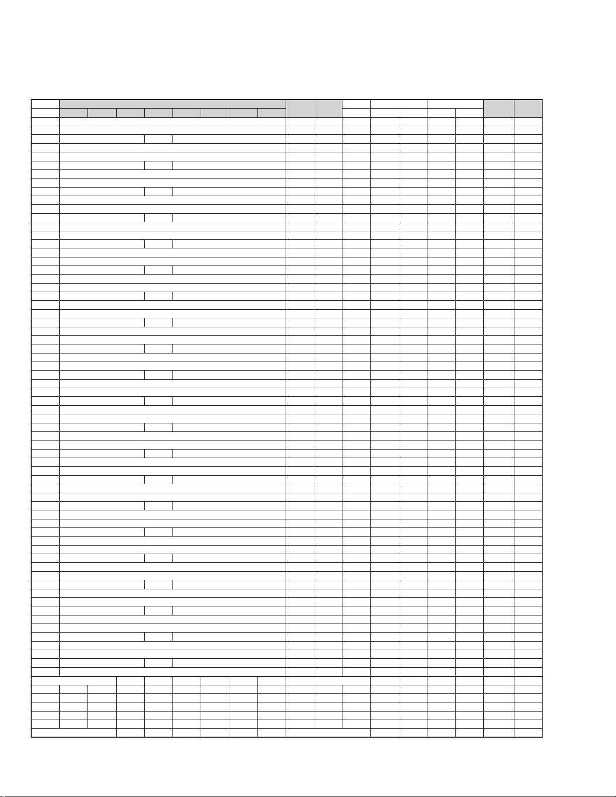
21C-FX1(C)/(G)
21C-FX5/FX8
MEMORY MAP
(Continued)
ADDRESS
DATA
(HEX) D7 D6 D5 D4 D3 D2 D1 D0
180
181
182
183
184
185
186
187
188
189
18A
18B
18C
18D
18E
18F
190
191
192
193
194
195
196
197
198
199
19A
19B
19C
19D
19E
19F
1A0
1A1
1A2
1A3
1A4
1A5
1A6
1A7
1A8
1A9
1AA
1AB
1AC
1AD
1AE
1AF
1B0
1B1
1B2
1B3
1B4
1B5
1B6
1B7
1B8
1B9
1BA
1BB
1BC
1BD
1BE
1BF
S-SYS AFT
S-SYS AFT
S-SYS AFT
S-SYS AFT
S-SYS AFT
S-SYS AFT
S-SYS AFT
S-SYS AFT
S-SYS AFT
S-SYS AFT
S-SYS AFT
S-SYS AFT
S-SYS AFT
S-SYS AFT
S-SYS AFT
S-SYS AFT
S-SYS AFT
S-SYS AFT
S-SYS AFT
S-SYS AFT
S-SYS AFT
TUNING FREQUANCY (HIGHER PART)
TUNING FREQUANCY (LOWER PART)
(auto) C-SYS
TUNING FREQUANCY (HIGHER PART)
TUNING FREQUANCY (LOWER PART)
(auto) C-SYS
TUNING FREQUANCY (HIGHER PART)
TUNING FREQUANCY (LOWER PART)
(auto) C-SYS
TUNING FREQUANCY (HIGHER PART)
TUNING FREQUANCY (LOWER PART)
(auto) C-SYS
TUNING FREQUANCY (HIGHER PART)
TUNING FREQUANCY (LOWER PART)
(auto) C-SYS
TUNING FREQUANCY (HIGHER PART)
TUNING FREQUANCY (LOWER PART)
(auto) C-SYS
TUNING FREQUANCY (HIGHER PART)
TUNING FREQUANCY (LOWER PART)
(auto) C-SYS
TUNING FREQUANCY (HIGHER PART)
TUNING FREQUANCY (LOWER PART)
(auto) C-SYS
TUNING FREQUANCY (HIGHER PART)
TUNING FREQUANCY (LOWER PART)
(auto) C-SYS
TUNING FREQUANCY (HIGHER PART)
TUNING FREQUANCY (LOWER PART)
(auto) C-SYS
TUNING FREQUANCY (HIGHER PART)
TUNING FREQUANCY (LOWER PART)
(auto) C-SYS
TUNING FREQUANCY (HIGHER PART)
TUNING FREQUANCY (LOWER PART)
(auto) C-SYS
TUNING FREQUANCY (HIGHER PART)
TUNING FREQUANCY (LOWER PART)
(auto) C-SYS
TUNING FREQUANCY (HIGHER PART)
TUNING FREQUANCY (LOWER PART)
(auto) C-SYS
TUNING FREQUANCY (HIGHER PART)
TUNING FREQUANCY (LOWER PART)
(auto) C-SYS
TUNING FREQUANCY (HIGHER PART)
TUNING FREQUANCY (LOWER PART)
(auto) C-SYS
TUNING FREQUANCY (HIGHER PART)
TUNING FREQUANCY (LOWER PART)
(auto) C-SYS
TUNING FREQUANCY (HIGHER PART)
TUNING FREQUANCY (LOWER PART)
(auto) C-SYS
TUNING FREQUANCY (HIGHER PART)
TUNING FREQUANCY (LOWER PART)
(auto) C-SYS
TUNING FREQUANCY (HIGHER PART)
TUNING FREQUANCY (LOWER PART)
(auto) C-SYS
TUNING FREQUANCY (HIGHER PART)
TUNING FREQUANCY (LOWER PART)
(auto) C-SYS
TUNING FREQUANCY (HIGHER PART)
MODEL MODEL
MICON EEPROM
DEFAULT
EEPROM CHASSIS CTV FINAL
RANGE WRITE(CPU) CHECK DATA CHECK TYPE CHECK DATA CHECK TYPE
10
10
10
10
10
10
10
10
10
10
10
10
10
10
10
10
10
10
10
10
10
LAST INITIAL
SETTING DATA
REMARK
POS 34
POS 35
POS 36
POS 37
POS 38
POS 39
POS 40
POS 41
POS 42
POS 43
POS 44
POS 45
POS 46
POS 47
POS 48
POS 49
POS 50
POS 51
POS 52
POS 53
POS 54
POS 55
LETTER NO. LETTER NO.
20
Page 21

MEMORY MAP
(Continued)
21C-FX1(C)/(G)
21C-FX5/FX8
ADDRESS
DATA
(HEX) D7 D6 D5 D4 D3 D2 D1 D0
1C0
1C1
1C2
1C3
1C4
1C5
1C6
1C7
1C8
1C9
1CA
1CB
1CC
1CD
1CE
1CF
1D0
1D1
1D2
1D3
1D4
1D5
1D6
1D7
1D8
1D9
1DA
1DB
1DC
1DD
1DE
1DF
1E0
1E1
1E2
1E3
1E4
1E5
1E6
1E7
1E8
1E9
1EA
1EB
1EC
1ED
1EE
1EF
1F0
1F1
1F2
1F3
1F4
1F5
1F6
1F7
1F8
1F9
1FA
1FB
1FC
1FD
1FE
1FF
S-SYS
S-SYS
S-SYS
S-SYS
S-SYS
S-SYS
S-SYS
S-SYS
S-SYS
S-SYS
S-SYS
S-SYS
S-SYS
S-SYS
S-SYS
S-SYS
S-SYS
S-SYS
S-SYS
S-SYS
S-SYS
TUNING FREQUANCY (LOWER PART) POS 55
AFT
TUNING FREQUANCY (HIGHER PART) POS 56
TUNING FREQUANCY (LOWER PART)
AFT
TUNING FREQUANCY (HIGHER PART) POS 57
TUNING FREQUANCY (LOWER PART)
AFT
TUNING FREQUANCY (HIGHER PART) POS 58
TUNING FREQUANCY (LOWER PART)
AFT
TUNING FREQUANCY (HIGHER PART) POS 59
TUNING FREQUANCY (LOWER PART)
AFT
TUNING FREQUANCY (HIGHER PART) POS 60
TUNING FREQUANCY (LOWER PART)
AFT
TUNING FREQUANCY (HIGHER PART) POS 61
TUNING FREQUANCY (LOWER PART)
AFT
TUNING FREQUANCY (HIGHER PART) POS 62
TUNING FREQUANCY (LOWER PART)
AFT
TUNING FREQUANCY (HIGHER PART) POS 63
TUNING FREQUANCY (LOWER PART)
AFT
TUNING FREQUANCY (HIGHER PART) POS 64
TUNING FREQUANCY (LOWER PART)
AFT
TUNING FREQUANCY (HIGHER PART) POS 65
TUNING FREQUANCY (LOWER PART)
AFT
TUNING FREQUANCY (HIGHER PART) POS 66
TUNING FREQUANCY (LOWER PART)
AFT
TUNING FREQUANCY (HIGHER PART) POS 67
TUNING FREQUANCY (LOWER PART)
AFT
TUNING FREQUANCY (HIGHER PART) POS 68
TUNING FREQUANCY (LOWER PART)
AFT
TUNING FREQUANCY (HIGHER PART) POS 69
TUNING FREQUANCY (LOWER PART)
AFT
TUNING FREQUANCY (HIGHER PART) POS 70
TUNING FREQUANCY (LOWER PART)
AFT
TUNING FREQUANCY (HIGHER PART) POS 71
TUNING FREQUANCY (LOWER PART)
AFT
TUNING FREQUANCY (HIGHER PART) POS 72
TUNING FREQUANCY (LOWER PART)
AFT
TUNING FREQUANCY (HIGHER PART) POS 73
TUNING FREQUANCY (LOWER PART)
AFT
TUNING FREQUANCY (HIGHER PART) POS 74
TUNING FREQUANCY (LOWER PART)
AFT
TUNING FREQUANCY (HIGHER PART) POS 75
TUNING FREQUANCY (LOWER PART)
AFT
TUNING FREQUANCY (HIGHER PART) POS 76
TUNING FREQUANCY (LOWER PART)
(auto) C-SYS
(auto) C-SYS
(auto) C-SYS
(auto) C-SYS
(auto) C-SYS
(auto) C-SYS
(auto) C-SYS
(auto) C-SYS
(auto) C-SYS
(auto) C-SYS
(auto) C-SYS
(auto) C-SYS
(auto) C-SYS
(auto) C-SYS
(auto) C-SYS
(auto) C-SYS
(auto) C-SYS
(auto) C-SYS
(auto) C-SYS
(auto) C-SYS
(auto) C-SYS
MODEL
MICON EEPROM EEPROM CHASSIS
DEFAULT RANGE
WRITE(CPU) CHECK DATA CHECK TYPE
10
10
10
10
10
10
10
10
10
10
10
10
10
10
10
10
10
10
10
10
10
MODEL
CTV FINAL
CHECK DATA CHECK TYPE SETTING DATA
LAST INITIAL
REMARK
LETTER NO.
LETTER NO.
21
Page 22

21C-FX1(C)/(G)
21C-FX5/FX8
MEMORY MAP
(Continued)
ADDRESS
DATA
(HEX) D7 D6 D5 D4 D3 D2 D1 D0
200
201
202
203
204
205
206
207
208
209
20A
20B
20C
20D
20E
20F
210
211
212
213
214
215
216
217
218
219
21A
21B
21C
21D
21E
21F
220
221
222
223
224
225
226
227
228
229
22A
22B
22C
22D
22E
22F
230
231
232
233
234
235
236
237
238
239
23A
23B
23C
23D
23E
23F
S-SYS
S-SYS
S-SYS
S-SYS
S-SYS
S-SYS
S-SYS
S-SYS
S-SYS
S-SYS
S-SYS
S-SYS
S-SYS
S-SYS
S-SYS
S-SYS
S-SYS
S-SYS
S-SYS
S-SYS
S-SYS
S-SYS
AFT
TUNING FREQUANCY (HIGHER PART)
TUNING FREQUANCY (LOWER PART)
AFT
TUNING FREQUANCY (HIGHER PART)
TUNING FREQUANCY (LOWER PART)
AFT
TUNING FREQUANCY (HIGHER PART)
TUNING FREQUANCY (LOWER PART)
AFT
TUNING FREQUANCY (HIGHER PART)
TUNING FREQUANCY (LOWER PART)
AFT
TUNING FREQUANCY (HIGHER PART)
TUNING FREQUANCY (LOWER PART)
AFT
TUNING FREQUANCY (HIGHER PART)
TUNING FREQUANCY (LOWER PART)
AFT
TUNING FREQUANCY (HIGHER PART)
TUNING FREQUANCY (LOWER PART)
AFT
TUNING FREQUANCY (HIGHER PART)
TUNING FREQUANCY (LOWER PART)
AFT
TUNING FREQUANCY (HIGHER PART)
TUNING FREQUANCY (LOWER PART)
AFT
TUNING FREQUANCY (HIGHER PART)
TUNING FREQUANCY (LOWER PART)
AFT
TUNING FREQUANCY (HIGHER PART)
TUNING FREQUANCY (LOWER PART)
AFT
TUNING FREQUANCY (HIGHER PART)
TUNING FREQUANCY (LOWER PART)
AFT
TUNING FREQUANCY (HIGHER PART)
TUNING FREQUANCY (LOWER PART)
AFT
TUNING FREQUANCY (HIGHER PART)
TUNING FREQUANCY (LOWER PART)
AFT
TUNING FREQUANCY (HIGHER PART)
TUNING FREQUANCY (LOWER PART)
AFT
TUNING FREQUANCY (HIGHER PART)
TUNING FREQUANCY (LOWER PART)
AFT
TUNING FREQUANCY (HIGHER PART)
TUNING FREQUANCY (LOWER PART)
AFT
TUNING FREQUANCY (HIGHER PART)
TUNING FREQUANCY (LOWER PART)
AFT
TUNING FREQUANCY (HIGHER PART)
TUNING FREQUANCY (LOWER PART)
AFT
TUNING FREQUANCY (HIGHER PART)
TUNING FREQUANCY (LOWER PART)
AFT
TUNING FREQUANCY (HIGHER PART)
TUNING FREQUANCY (LOWER PART)
AFT
(auto) C-SYS
(auto) C-SYS
(auto) C-SYS
(auto) C-SYS
(auto) C-SYS
(auto) C-SYS
(auto) C-SYS
(auto) C-SYS
(auto) C-SYS
(auto) C-SYS
(auto) C-SYS
(auto) C-SYS
(auto) C-SYS
(auto) C-SYS
(auto) C-SYS
(auto) C-SYS
(auto) C-SYS
(auto) C-SYS
(auto) C-SYS
(auto) C-SYS
(auto) C-SYS
(auto) C-SYS
MODEL MODEL
MICON EEPROM EEPROM CHASSIS CTV FINAL
DEFAULT RANGE
WRITE(CPU) CHECK DATA CHECK TYPE CHECK DATA
10
10
10
10
10
10
10
10
10
10
10
10
10
10
10
10
10
10
10
10
10
10
LAST INITIAL
CHECK TYPE SETTING DATA
REMARK
POS 77
POS 78
POS 79
POS 80
POS 81
POS 82
POS 83
POS 84
POS 85
POS 86
POS 87
POS 88
POS 89
POS 90
POS 91
POS 92
POS 93
POS 94
POS 95
POS 96
POS 97
LETTER NO. LETTER NO.
22
Page 23

MEMORY MAP
250
251
252
253
254
255
256
257
258
259
25A
25B
25C
25D
25E
25F
260
261
262
263
264
265
266
267
268
269
26A
26B
26C
26D
26E
26F
270
271
272
273
274
275
276
277
278
279
27A
27B
27C
27D
27E
27F
MODEL MODEL
LETTER NO. LETTER NO.
240
241
242
S-SYS
243
244
245
S-SYS
246
247
248
249
24A
24B
24C
24D
24E
24F
POS 98
10
POS 99
10
AV1
10
AV2
10
GAME
10
TUNING FREQUANCY (HIGHER PART)
TUNING FREQUANCY (LOWER PART)
AFT
TUNING FREQUANCY (HIGHER PART)
TUNING FREQUANCY (LOWER PART)
AFT
(auto) C-SYS
(auto) C-SYS
(auto) C-SYS
(auto) C-SYS
(auto) C-SYS
ADDRESS
DATA
MICON EEPROM
(HEX) D7 D6 D5 D4 D3 D2 D1 D0
DEFAULT RANGE
EEPROM CHASSIS CTV FINAL
LAST INITIAL
WRITE(CPU) CHECK DATA CHECK TYPE CHECK DATA CHECK TYPE SETTING DATA
REMARK
1E 00-3C
DEFAULT BALANCE-G
1E 00-3C
DEFAULT BASS-G
1E 00-3C
00 00-02
DEFAULT TREBLE-G
DEFAULT SURR ON-G
00 00-02
DEFAULT SPAT ON-G
1E 00-3C
DEFAULT SURROUND LEVEL-G
1E 00-3C
DEFAULT SPATIALIZER LEVEL-G
3C 00-3C
DEFAULT CONTRAST-G
1E 00-3C
DEFAULT COLOUR-G
1E 00-3C
DEFAULT BRIGHTNESS-G
1E 00-3C
DEFAULT TINT-G
1E 00-3C
DEFAULT SHARPNESS-G
00 00-02
DEFAULT WHITE TEMP-G
(Continued)
21C-FX1(C)/(G)
21C-FX5/FX8
23
Page 24

21C-FX1(C)/(G)
21C-FX5/FX8
MEMORY MAP
(Continued)
ADDRESS
DATA
(HEX) D7 D6 D5 D4 D3 D2 D1 D0
280
281
282
283
284
285
286
287
288
289
28A
28B
28C
28D
28E
28F
290
291
292
293
294
295
296
297
298
299
29A
29B
29C
29D
29E
29F
2A0
2A1
2A2
2A3
2A4
2A5
2A6
2A7
2A8
2A9
2AA
2AB
2AC
2AD
2AE
2AF
2B0
2B1
2B2
2B3
2B4
2B5
2B6
2B7
2B8
2B9
2BA
2BB
2BC
2BD
2BE
2BF
MODEL MODEL
MICON EEPROM EEPROM CHASSIS CTV FINAL
DEFAULT RANGE
WRITE(CPU) CHECK DATA CHECK TYPE CHECK DATA CHECK TYPE
LAST INITIAL
SETTING DATA
REMARK
LETTER NO. LETTER NO.
24
Page 25

MEMORY MAP
(Continued)
21C-FX1(C)/(G)
21C-FX5/FX8
ADDRESS
(HEX)
2C0
2C1
2C2
2C3
2C4
2C5
2C6
2C7
2C8
2C9
2CA
2CB
2CC
2CD
2CE
2CF
2D0
2D1
2D2
2D3
2D4
2D5
2D6
2D7
2D8
2D9
2DA
2DB
2DC
2DD
2DE
2DF
2E0
2E1
2E2
2E3
2E4
2E5
2E6
2E7
2E8
2E9
2EA
2EB
2EC
2ED
2EE
2EF
2F0
2F1
2F2
2F3
2F4
2F5
2F6
2F7
2F8
2F9
2FA
2FB
2FC
2FD
2FE
2FF
D7 D6 D5 D4 D3 D2 D1 D0
DATA
MODEL MODEL
MICON EEPROM EEPROM CHASSIS CTV FINAL
DEFAULT RANGE
WRITE(CPU) CHECK DATA CHECK TYPE CHECK DATA CHECK TYPE
LAST INITIAL
SETTING DATA
REMARK
LETTER NO. LETTER NO.
25
Page 26

TROUBLE SHOOTING TABLE
NO RASTER
Blown out.
Replace the fuse.
Check IC701, D701 and
C707.
The fuse is again blown out.
Does horizontal circuit
oscillate ?
D1001 (Power LED Red)
turns on or turns ON/OFF.
Check T701 pin (7) voltage
(Approx. 310V at 220V AC)
Check F701.
Check Secondary Main+B
(Approx. 120V)
Check CRT connector K1K5 bias.
Check IC605, IC751 and
IC801.
Check
C878.
Check
IC801.
Checking the
protector circuit.
Check R615.
D1001 (Power LED red)
turns on and off.
See many often D1001
flashes in red.
This indicates which IC to
check up.
D1001 (Power LED Green)
turns on.
Check D758, IC702, IC753
and D762.
Check R701, R707 and
D709.
LIGHTS UP
TURN OFF
TV PROCESSORE
(IC801)
EEP ROM
(IC1003)
AV SWITCH
(IC401)
SOUND PRPCESSOR
(IC305)
(NICAM/IGR) DECODER
(IC2300)
TUNER
(TU201)
(Bus error)
TROUBLE SHOOTING TABLE (Continued)
NO PICTURE, NO SOUND
Does noise signal appear at
pins (3) and (22) of IC305 ?
NO SOUND
No snow noise.
Does noise or signal appear at pin (40)
of IC801 ?
Noise increases but no signal is
received.
Check the tuner supply voltage LB and
HB must be approx. 5V. BT must be
approx. 32V. and CH preset data check.
Check the tuner AGC at
TP201.
Does noise or
signal appear at
pin (38) of IC801 ?
Check IC801 and
its related circuit.
Check IC401 and
related circuit.
Check pin (1) of
SF201, Tuner and
related circuit.
Check pin (37)of
IC801 and related
circuit.
Check pin (27) of
IC801, Tuner and
related circuit.
Check pin(38) of
IC801.
Does the noise level increase at max.
Contrast, Brightness and Sound controls ?
CIRCUITS TO BE CHECKED:
» Tuner.
» PIF.
» Automatic Gain Control.
» (5V), (32V) Power Source.
CIRCUITS TO BE CHECKED:
» Sound Detector Circuit.
» Sound Switch and Att.
Control.
» Audio Output Circuit.
Does signal appear at pins
(2) and (5) of IC302 ?
Is there audio signal at pins (3)
and (5) of SC2300?
(NICAM/IGR unit socket)
Check TV sound.
Check Speaker.
Does noise or
signal appear at
pin (23) and (24)
of IC801 ?
Check IC302 and
peripheral circuit.
Check IC401.
Check NICAM/
IGR unit, tuner
and its peripheral
circuit.
*NOTE:
NICAM/IGR for model
21C-FX5/8 .
21C-FX1(C)/(G)
21C-FX5/FX8
26
26-1 26-2
Page 27

TROUBLE SHOOTING TABLE
(Continued)
NEITHER VERTICAL NOR
HORIZONTAL SYNCHRONIZATION
CIRCUIT TO BE CHECKED:
» Sync. Separator Circuit.
NO VERTICAL SCAN
Vertical linearity and size is
abnormal.
Check pins(33) and (34) of
IC801.
DEFECTIVE VERTICAL AMP.
AND VERTICAL LINEARITY
Readjust vertical size.
(Bas Data)
Check IC501.
Check C506 and C507.
Check IC501 bias.
Check R504, R503, R506,
R513 and C517.
TROUBLE SHOOTING TABLE
(Continued)
NO SPECIFIC COLOUR
Is some colour produced in
B/W broadcast reception ?
Is the white balance properly
adjusted ?
Readjust the white balance.
The picture colour is yellow.
The picture colour is magenta.
The picture colour is cyan.
Check Q870, Q885 and their
adjacent circuits.
Check Q871, Q883 and their
adjacent circuits.
Check Q872, Q887 and their
adjacent circuits.
Check IC801 and bias
control circuit.
NO SPECIFIC COLOUR
“PAL / SECAM / NTSC”
(NO COLOUR SYNCHRONIZATION)
Check IC801, R801, R802,
R803, D804, D805, D806
and Q801.
Check X1001.(12MHz)
Check Q251 and peripheral
circuit.
(PAL / SECAM) (NTSC)
27
27-1 27-2
21C-FX1(C)/(G)
21C-FX5/FX8
Page 28
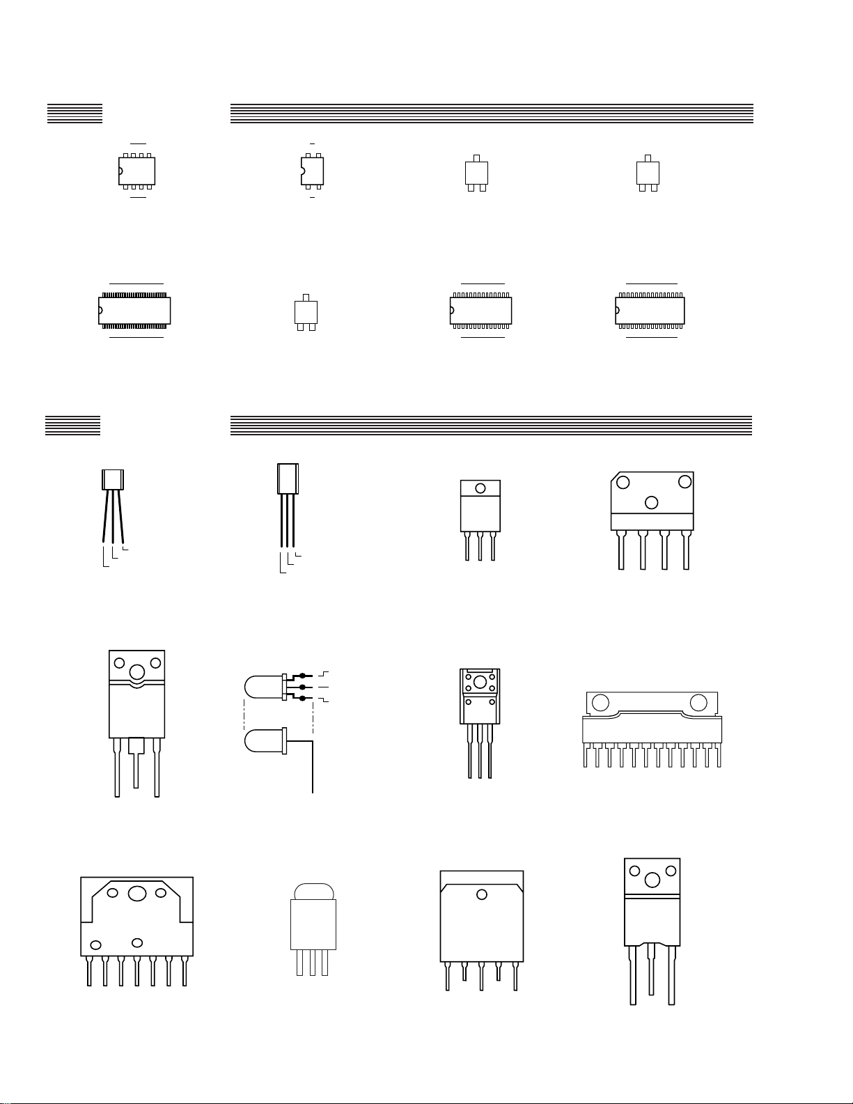
21C-FX1(C)/(G)
21C-FX5/FX8
TOP VIEW
SOLID STATE DEVICE BASE DIAGRAM
85
43
COLLECTOR
COLLECTOR
ZR
14
12
BASE EMITTER
BASE EMITTER
M24C08W FX0008GE D601A B709A
64 33
COLLECTOR
24 13
28 15
JC
132
iX3410CE
/iX3412CE
BASE EMITTER
2SC2735
112
AN5891
114
M52797
SIDE VIEW
+ ~ ~ -
:BG:
BASE
COLLECTOR
EMITTER
2SC1815
2SA1015
2
1
3
BASE
COLLECTOR
EMITTER
2SC2482 DX0386CE
ANODE
(RED)
CATHODE
(COMMON)
ANODE
(GREEN)
1 3
SE120N
123
KA7808
KA7805
112
AN5277PX0423CE2SD2634
LA7841
1
TA48M033
3
1
STRF6654
5
TF321S
28
Page 29

WAVEFORMS
1)
HorizRate HorizRate HorizRate HorizRate
HorizRate HorizRate HorizRate
HorizRate HorizRate HorizRate
HorizRate
HorizRateHorizRate
Vert Rate Vert Rate Vert Rate
Vert Rate
Vert Rate
0.98 Vp-p 4.08 Vp-p 3.68 Vp-p 4.2 Vp-p
88.8 Vp-p 107.2 Vp-p 109.6 Vp-p 3.32 Vp-p
2.28 Vp-p 138 Vp-p 9.12 Vp-p 0.13 Vp-p
0.18 Vp-p 5.72 Vp-p 55.2 Vp-p 170 Vp-p
1104 Vp-p 324 Vp-p(AC110V)
485 Vp-p(AC220V)
1.9 Vp-p
2) 3) 4)
8)7)6)5)
9) 10) 11) 12)
16)15)14)13)
17) 18) 19)
21C-FX1(C)/(G)
21C-FX5/FX8
31
Page 30

21C-FX1(C)/(G)
21C-FX5/FX8
SCHEMATIC DIAGRAM: CRT Unit
J
I
H
G
F
E
D
C
B
A
1 2 3 4 5 6 7 8 9 10
33
Page 31

21C-FX1(C)/(G)
21C-FX5/FX8
SCHEMATIC DIAGRAM: MAIN Unit -1/2
21C-FX1(C)/(G)
21C-FX5/FX8
J
I
H
G
F
(MODEL 21C-FX1(C)/(G) )
E
D
C
B
A
1 2 3 4 5 6 7 8 9 10
11 12 13 14 15 16 17 18 19
3534
Page 32

21C-FX1(C)/(G)
21C-FX5/FX8
SCHEMATIC DIAGRAM: MAIN Unit -1/2
21C-FX1(C)/(G)
21C-FX5/FX8
J
I
H
G
F
(MODEL 21C-FX5/FX8 )
E
D
C
B
A
1 2 3 4 5 6 7 8 9 10
11 12 13 14 15 16 17 18 19
3736
Page 33
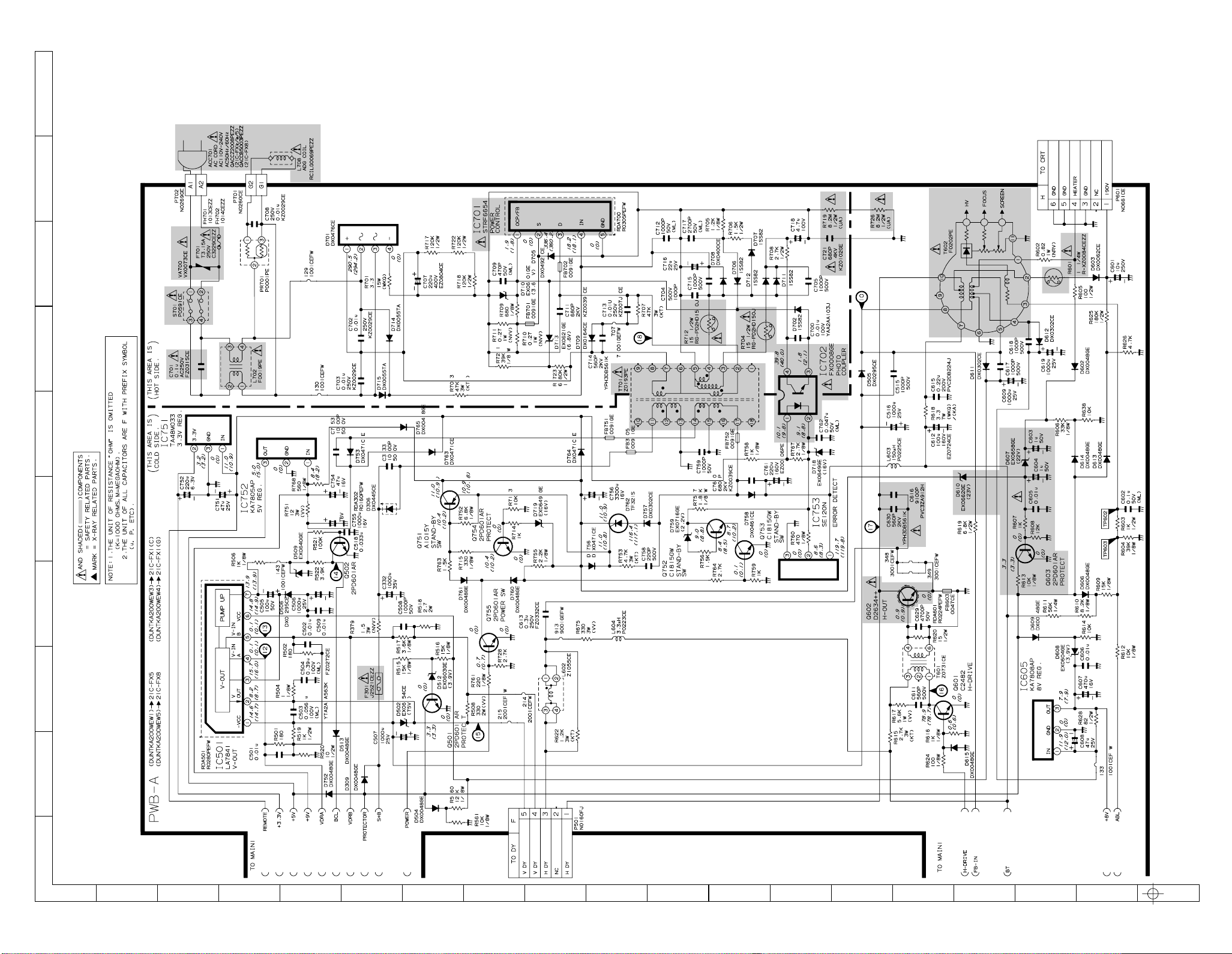
21C-FX1(C)/(G)
21C-FX5/FX8
SCHEMATIC DIAGRAM: MAIN Unit -2/2
J
I
H
G
21C-FX1(C)/(G)
21C-FX5/FX8
F
E
D
C
B
A
1 2 3 4 5 6 7 8 9 10
11 12 13 14 15 16 17 18 19
3938
Page 34
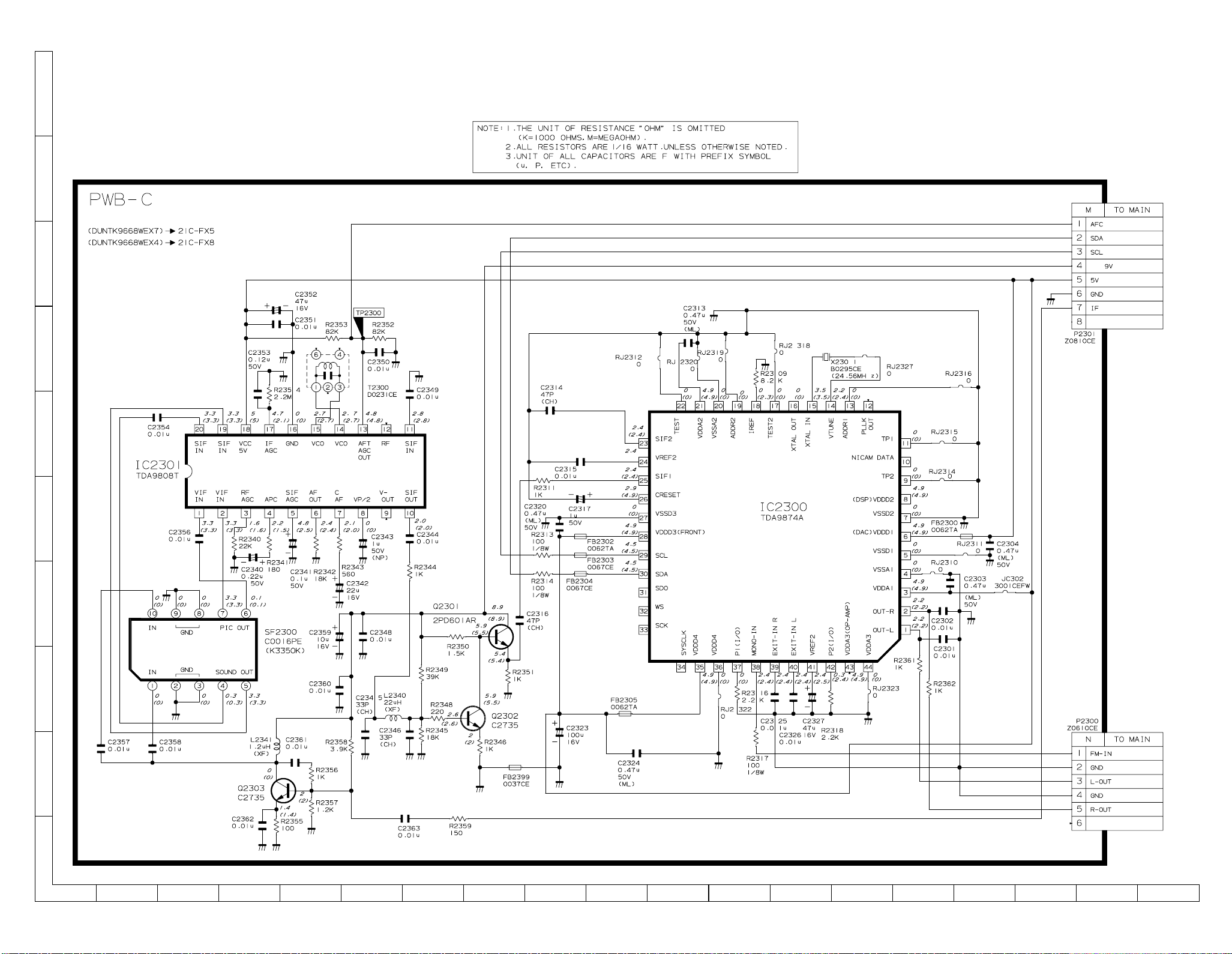
21C-FX1(C)/(G)
21C-FX5/FX8
SCHEMATIC DIAGRAM: NICAM Unit
21C-FX1(C)/(G)
21C-FX5/FX8
J
I
H
G
F
(MODEL 21C-FX5/FX8 )
E
D
C
B
A
1 2 3 4 5 6 7 8 9 10
11 12 13 14 15 16 17 18 19
4140
Page 35
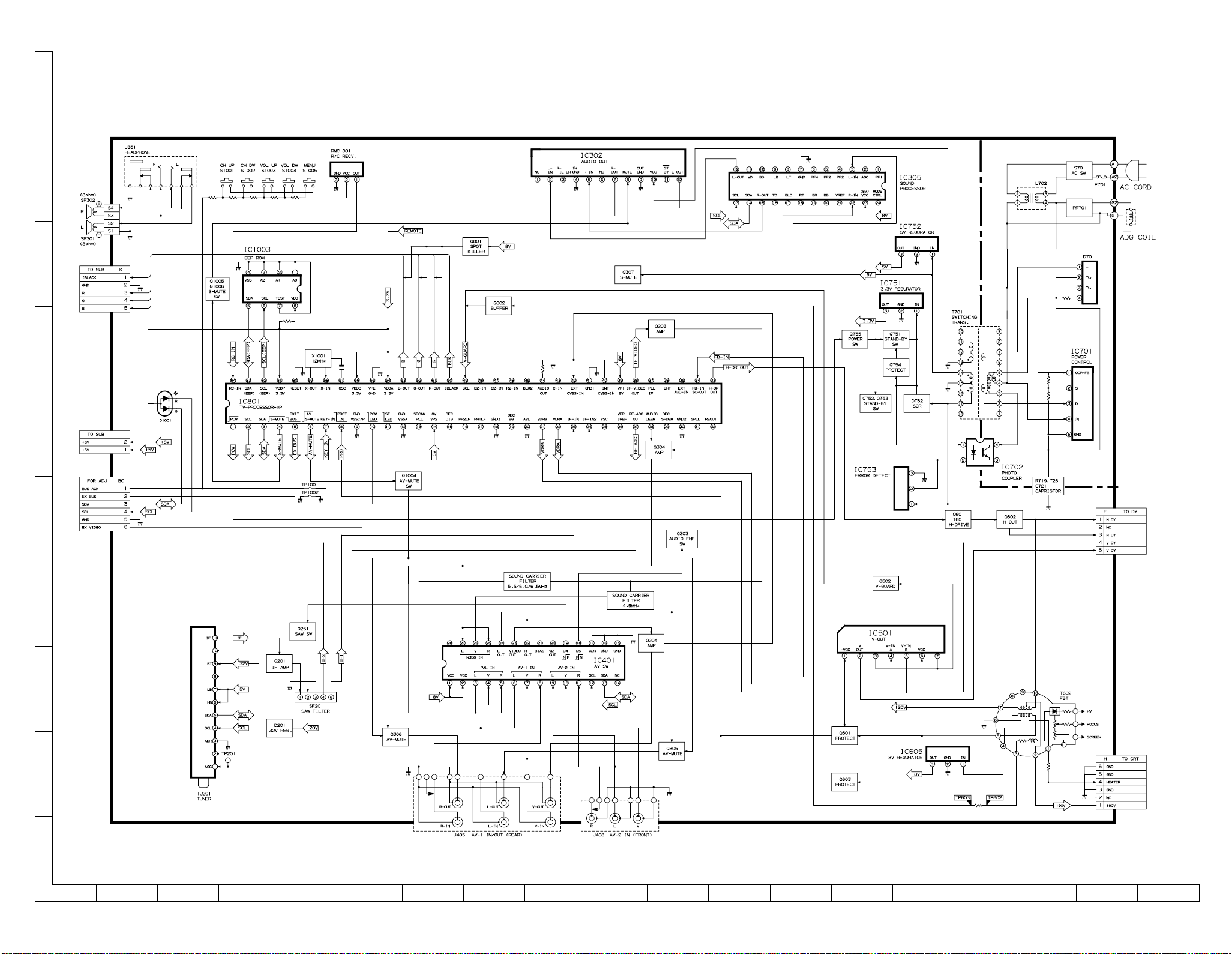
21C-FX1(C)/(G)
21C-FX5/FX8
BLOCK DIAGRAM - 1/3:MAIN BLOCK
21C-FX1(C)/(G)
21C-FX5/FX8
J
MODEL 21C-FX1(C)/1(G)
PWB-A MAIN BLOCK
I
H
G
F
E
D
C
B
A
1 2 3 4 5 6 7 8 9 10
11 12 13 14 15 16 17 18 19
4342
Page 36

21C-FX1(C)/(G)
21C-FX5/FX8
BLOCK DIAGRAM - 2/3:MAIN BLOCK
21C-FX1(C)/(G)
21C-FX5/FX8
J
MODEL 21C-FX5/FX8
PWB-A MAIN BLOCK
I
H
G
F
E
D
C
B
A
1 2 3 4 5 6 7 8 9 10
11 12 13 14 15 16 17 18 19
4544
Page 37

21C-FX1(C)/(G)
21C-FX5/FX8
BLOCK DIAGRAM - 3/3:
J
CRT / NICAM BLOCK
I
PWB-B CRT BLOCK
H
G
F
PWB-C NICAM BLOCK
(MODEL 21C-FX5/FX8)
E
D
C
B
A
1 2 3 4 5 6 7 8 9 10
46
Page 38

21C-FX1(C)/(G)
21C-FX5/FX8
Ref. No. Part No. Description Code
PARTS LIST
PARTS REPLACEMENT
Replacement parts which have these special safety characteristics
are identified in this manual; electrical components having such
features are identified by "å" in the Replacement Parts Lists.
The use of a substitute replacement part which does not have the
same safety characteristics as the factory recommended replacement parts shown in this service manual may create shock, fire or
other hazards.
"HOW TO ORDER REPLACEMENT PARTS"
To have your order filled promptly and correctly, please furnish the
following informations.
1. MODEL NUMBER 2. REF. NO.
3. PART NO. 4. DESCRIPTION
MARK : SPARE PARTS-DELIVERY SECTION.
Ref. No. Part No. Description Code
PICTURE TUBE
å V801 VB51QDJ279X2E R Picture Tube CG
å L708 RCiLG0069PEZZ R Degaussing Coil AR
RCiLHA010WJZZ R Deflection Yoke BF
PMAGF3046CEZZ R Magnet AF
QEARC2122PEZZ R Grounding Strap AF
LHLDW0003PEKZ R ADG Holder, x4 AB
MSPRT0001PEFJ R Spring, Grounding Strap AC
PSPAG0003PEZZ R Wedge, x3 AD
PRINTED WIRING BOARD ASSEMBLY
(NOT REPLACEMENT ITEM)
PWB-A DUNTKA200FMW3 - Main Unit (21C-FX1(C)) —
PWB-A DUNTKA200FMW4 - Main Unit (21C-FX1(G)) —
PWB-A DUNTKA200FMW1 - Main Unit (21C-FX5) —
PWB-A DUNTKA200FMW5 - Main Unit (21C-FX8) —
PWB-B DUNTK9990WEC2 - CRT Unit (21C-FX1(C)) —
PWB-B DUNTK9990WEC3 - CRT Unit (21C-FX1(G)) —
PWB-B DUNTK9990WEB9 - CRT Unit (21C-FX5) —
PWB-B DUNTK9990WEC4 - CRT Unit (21C-FX8) —
PWB-C DUNTK9668FMX1 - NICAM Unit (21C-FX5) —
PWB-C DUNTK9668FMX4 - NICAM Unit (21C-FX8) —
DUNTKA200FMW3/W4/W1/W5
MAIN UNIT
TUNER AND ASSEMBL Y
NOTE: THE PARTS HERE SHOWN ARE SUPPLIED AS AN
ASSEMBLY BUT INDEPENDENTLY.
å TU201 VTUVTST5HD970 R VHF Tuner AY
INTEGRATED CIRCUITS
IC302 VHiAN5277//-1 R AN5277 AN
IC305 VHiAN5891K+-1 R AN5891K AQ
IC401 VHiM52797SP-1 R M52797SP AP
IC501 VHiLA7841//-1 R LA7841 AM
IC605 VHiKA7808AP-1 R KIA7808API AE
å IC701 VHiSTRF6654-1 R STR-F6654 AX
Ref. No. Part No. Description Code
IC751 VHiTA48M033-1 R TA48M033F AH
IC752 VHiKA7805AP-1 R KIA7805API AE
IC753 VHiSE120N//-1 R SE120N AG
IC801 RH-iX3410CEN5 R I.C. (21C-FX1(C)/(G), FX8) BD
IC801 RH-iX3412CEN5 R I.C. (21C-FX5) BK
IC1003 VHiM24C08W/-1 R M24C08-WBN6 AH
TRANSISTORS
Q201 VS2SC2735//1E R 2SC2735 AC
Q203 VS2PD601AR/-1 R 2PD601AR AB
Q204 VS2PD601AR/-1 R 2PD601AR AB
Q251 VS2PD601AR/-1 R 2PD601AR AB
Q303 VS2PD601AR/-1 R 2PD601AR AB
Q304 VS2PD601AR/-1 R 2PD601AR AB
Q305 VS2PD601AR/-1 R 2PD601AR AB
Q306 VS2PD601AR/-1 R 2PD601AR AB
Q307 VS2PB709AR/-1 R 2PB709AR AB
Q501 VS2PD601AR/-1 R 2PD601AR AB
Q502 VS2PD601AR/-1 R 2PD601AR AB
Q601 VS2SC2482//-1 R 2SC2482 AD
å Q602 VS2SD2634++-G R 2SD2634++ AM
å Q603 VS2PD601AR/-1 R 2PD601AR AB
Q751 VS2SA1015Y/1E R 2SA1015Y AC
Q752 VS2SC1815GW-1 R 2SC1815GW AB
Q753 VS2SC1815GW-1 R 2SC1815GW AB
Q754 VS2PD601AR/-1 R 2PD601AR AB
Q755 VS2PD601AR/-1 R 2PD601AR AB
Q801 VS2PB709AR/-1 R 2PB709AR AB
Q802 VS2PB709AR/-1 R 2PB709AR AB
Q1004 VS2PD601AR/-1 R 2PD601AR AB
Q1005 VS2PD601AR/-1 R 2PD601AR AB
Q1006 VS2PD601AR/-1 R 2PD601AR AB
DIODES
D201 RH-EX0676GEZZ R Zener Diode AA
D252 VHD1SS356//-1 R 1SS356 AB
D301 RH-DX0048GEZZ R Diode AA
D302 RH-EX0615GEZZ R Zener Diode AA
D303 RH-EX0615GEZZ R Zener Diode AA
D304 RH-EX0631GEZZ R Zener Diode AA
D305 RH-EX0631GEZZ R Zener Diode AA
D306 RH-DX0445CEZZ R Diode AL
D309 RH-DX0048GEZZ R Diode AA
D312 RH-DX0048GEZZ R Diode AA
D313 RH-DX0048GEZZ R Diode AA
D314 RH-DX0048GEZZ R Diode AA
D315 RH-DX0048GEZZ R Diode AA
D316 RH-DX0048GEZZ R Diode AA
D320 RH-DX0048GEZZ R Diode AA
D402 RH-EX0631GEZZ R Zener Diode AA
D403 RH-EX0867CEZZ R Zener Diode AC
D404 RH-EX0867CEZZ R Zener Diode AC
D502 RH-EX0654CEZZ R Zener Diode AD
D504 RH-DX0048GEZZ R Diode AA
D505 RH-DX0295CEZZ R Diode AD
D506 RH-DX0295CEZZ R Diode AD
D509 RH-EX0640GEZZ R Zener Diode AA
D512 RH-EX0603GEZZ R Zener Diode AA
D513 RH-DX0048GEZZ R Diode AA
D602 RH-DX0048GEZZ R Diode AA
D603 RH-DX0062CEZZ R Diode AD
D604 RH-EX0627GEZZ R Zener Diode AA
D606 RH-DX0048GEZZ R Diode AA
å D607 RH-EX0658GEZZ R Zener Diode AA
D608 RH-EX0604GEZZ R Zener Diode AB
D609 RH-DX0048GEZZ R Diode AA
å D610 RH-EX0662GEZZ R Zener Diode AB
D611 RH-DX0302CEZZ R Diode AC
D612 RH-DX0302CEZZ R Diode AC
D613 RH-DX0048GEZZ R Diode AA
D614 RH-DX0048GEZZ R Diode AA
D615 RH-DX0048GEZZ R Diode AA
D701 RH-DX0476CEZZ R Diode AG
D702 VHD1SS82///1A R 1SS82 AC
D705 RH-DX0492CEZZ R Diode AE
D706 VHD1SS82///1A R 1SS82 AC
52
Page 39

Ref. No. Part No. Description CodeRef. No. Part No. Description Code
D707 VHD1SS82///1A R 1SS82 AC
D708 RH-DX0400CEZZ R Diode AC
D709 RH-DX0164CEZZ R Diode AC
D710 RH-EX0601GEZZ R Zener Diode AA
D711 VHD1SS82///1A R 1SS82 AC
D712 VHD1SS82///1A R 1SS82 AC
D713 RH-EX0621GEZZ R Zener Diode AB
D714 RH-DX0055TAZZ R Diode AD
D715 RH-DX0055TAZZ R Diode AD
D718 RH-EX0649GEZZ R Zener Diode AB
D719 RH-EX0649GEZZ R Zener Diode AB
D752 RH-DX0048GEZZ R Diode AA
D753 RH-DX0471CEZZ R Diode AE
D756 RH-DX0471CEZZ R Diode AE
D757 RH-DX0302CEZZ R Diode AC
D758 RH-DX0461CEZZ R Diode AG
D759 RH-EX0716GEZZ R Zener Diode AB
D760 RH-DX0048GEZZ R Diode AA
D761 RH-DX0048GEZZ R Diode AA
D762 VHDTF321S//-1 R TF321S AH
D763 RH-DX0471CEZZ R Diode AE
D764 RH-DX0471CEZZ R Diode AE
D765 RH-DX0048GEZZ R Diode AA
D802 RH-DX0048GEZZ R Diode AA
D803 RH-DX0048GEZZ R Diode AA
D804 RH-DX0048GEZZ R Diode AA
D805 RH-DX0048GEZZ R Diode AA
D806 RH-DX0048GEZZ R Diode AA
D808 RH-EX0257TAZZY R Zener Diode AB
D1001 RH-PX0423CEZZ R PhotoDiode AD
D1004 RH-DX0048GEZZ R Diode AA
D1007 RH-EX0867CEZZ R Zener Diode AC
D1008 RH-EX0867CEZZ R Zener Diode AC
D1009 RH-EX0867CEZZ R Zener Diode AC
D1010 RH-EX0867CEZZ R Zener Diode AC
D1011 RH-DX0048GEZZ R Diode AA
D1017 RH-EX0612GEZZ R Zener Diode AA
å IC702 RH-FX0008GEZZ R PC123FY8 AE
P ACKAGED CIRCUITS
å VA700 RH-VX0073CEZZ R Varistor AD
PR701 RMPTP0001PEZZ R Packaged Circuit AN
X1001 RCRSB0300CEZZ R Crystal, 12MHz AF
COILS
L202 VP-DF270K0000 R Peaking 27µHAB
L203 VP-DF270K0000 R Peaking 27µHAB
L204 VP-XF1R2M0000 R Peaking 1.2µHAB
L205 VP-DF1R0M0000 R Peaking 1µHAB
L206 VP-DF1R0M0000 R Peaking 1µHAB
L208 VP-XF100K0000 R Peaking 10µHAB
L209 VP-XF6R8K0000 R Peaking 6.8µHAB
L210 VP-XF120K0000 R Peaking 12µHAB
L211 VP-CF270K0000 R Peaking 27µH (21C-FX5/FX8)AB
L401 VP-DF1R0M0000 R Peaking 1µHAB
L602 RCiLZ1055CEZZ R Coil AK
L603 RCiLP0225CEZZ R Coil AF
L604 RCiLP0223CEZZ R Coil AE
å L702 RCiLF0019PEZZ R Coil AN
L802 VP-DF100K0000 R Peaking 10µHAB
L803 VP-DF100K0000 R Peaking 10µHAB
L1001 VP-DF100K0000 R Peaking 10µHAB
L1002 VP-DF100K0000 R Peaking 10µHAB
L1003 VP-DF100K0000 R Peaking 10µHAB
FILTERS
CF201 RFiLC0024CEZZ R Filter AE
CF202 RFiLC0318CEZZ R Filter AG
CF203 RFiLC0446CEZZ R Filter AD
SF201 RFiLC0037PEZZ R Filter AP
TRANSFORMERS
T601 RTRNZ0731CEZZ R Transformer AG
å T602 RTRNF0202PEZZ R H-Volt Transformer BA
å T701 RTRNZ0193PEZZ R Transformer AQ
C200 VCEA0A1CW476M R 47 16V Electrolytic AB
C203 VCKYCY1HF103Z R 0.01 50V Ceramic AA
C204 VCEA0A1CW108M R 1000 16V Electrolytic AD
C204 VCEA0A1CW477M R 470 16V Electrolytic AC
C205 VCKYCY1HF103Z R 0.01 50V Ceramic AA
C206 VCEA0A1HW106M R 10 50V Electrolytic AB
C207 VCKYCY1HF103Z R 0.01 50V Ceramic AA
C208 VCKYCY1HF103Z R 0.01 50V Ceramic AA
C209 VCKYCY1HF103Z R 0.01 50V Ceramic AA
C210 VCKYCY1HF103Z R 0.01 50V Ceramic AA
C211 VCKYCY1EF104Z R 0.1 25V Ceramic AA
C212 VCEA0A1CW106M R 10 16V Electrolytic AB
C213 VCKYCY1HF223Z R 0.022 50V Ceramic AB
C214 VCEA0A1CW226M R 22 16V Electrolytic AB
C216 VCKYCY1HB821K R 820p 50V Ceramic AA
C217 VCKYCY1HB472K R 4700p 50V Ceramic AA
C218 VCKYCY1HF103Z R 0.01 50V Ceramic AA
C306 VCEA0A1EW107M R 100 25V Electrolytic AC
C307 VCEA0A1HW105M R 1 50V Electrolytic AB
C308 VCEA0A1EW108M R 1000 25V Electrolytic AD
C309 VCEA0A1HW225M R 2.2 50V Electrolytic AB
C310 VCEA0A1CW336M R 33 16V Electrolytic AB
C311 VCEA0A1EW108M R 1000 25V Electrolytic AD
C312 VCQYTA1HM102J R 1000p 50V Mylar AA
C313 VCQYTA1HM102J R 1000p 50V Mylar AA
C314 VCEA0A1VW108M R 1000 35V Electrolytic AD
C315 VCKYPA1HF103Z R 0.01 50V Ceramic AA
C316 VCEA0A1CW106M R 10 16V Electrolytic AB
C317 VCEA0A1CW106M R 10 16V Electrolytic AB
C319 VCEA0A1HW105M R 1 50V Electrolytic AB
C322 VCEA0A1CW106M R 10 16V Electrolytic AB
C323 VCEA0A1CW106M R 10 16V Electrolytic AB
C327 VCQYTA1HM103J R 0.01 50V Mylar AA
C328 VCEA0A1HW104M R 0.1 50V Electrolytic AB
C329 VCEA0A1CW106M R 10 16V Electrolytic AB
C330 VCEA0A1CW106M R 10 16V Electrolytic AB
C331 VCEA0A1HW105M R 1 50V Electrolytic AB
C332 VCEA0A1VW108M R 1000 35V Electrolytic AD
C333 VCKYPA2HB102K R 1000p 500V Ceramic AA
C337 VCQYTA1HM392J R 3900p 50V Mylar AA
C338 VCQYTA1HM103J R 0.01 50V Mylar AA
C339 VCQYTA1HM333J R 0.033 50V Mylar AA
C340 VCEA0A1CW106M R 10 16V Electrolytic AB
C341 VCEA0A1CW106M R 10 16V Electrolytic AB
C342 VCEA0A1CW106M R 10 16V Electrolytic AB
C343 VCQYTA1HM103J R 0.01 50V Mylar AA
C344 VCEA0A1HW104M R 0.1 50V Electrolytic AB
C346 VCEA0A1CW106M R 10 16V Electrolytic AB
C347 VCEA0A1CW106M R 10 16V Electrolytic AB
C348 VCKYPA1HF103Z R 0.01 50V Ceramic AA
C349 VCEA0A1CW107M R 100 16V Electrolytic AC
C350 VCEA0A1CW106M R 10 16V Electrolytic AB
C352 VCQYTA1HM103J R 0.01 50V Mylar AA
C355 VCEA0A1CW106M R 10 16V Electrolytic AB
C356 VCKYCY1HB682K R 6800p 50V Ceramic AA
C357 VCKYCY1HB182K R 1800p 50V Ceramic AA
C359 VCEA0A1CW106M R 10 16V Electrolytic AB
C361 VCE9GA1CW106M R 10 16V Elect. (N.P) AB
C361 VCEA0A1CW106M R 10 16V Electrolytic AB
C362 VCEA0A1CW106M R 10 16V Electrolytic AB
C363 VCEA0A1CW106M R 10 16V Electrolytic AB
C364 VCEA0A1CW106M R 10 16V Electrolytic AB
C365 VCKYCY1EF104Z R 0.1 25V Ceramic AA
C367 VCCCCY1HH221J R 220p 50V Ceramic AA
C368 VCCCCY1HH221J R 220p 50V Ceramic AA
C369 VCEA0A1HW105M R 1 50V Electrolytic AB
C370 VCEA0A1HW105M R 1 50V Electrolytic AB
21C-FX1(C)/(G)
21C-FX5/FX8
CAPACITORS
(21C-FX5/FX8)
(21C-FX1(C)/(G))
(21C-FX5/FX8)
(21C-FX1(G)/FX8)
(21C-FX1(G)/FX8)
(21C-FX1(C)/(G))
(21C-FX5/FX8)
(21C-FX5/FX8)
53
Page 40

21C-FX1(C)/(G)
21C-FX5/FX8
Ref. No. Part No. Description Code
C371 VCEA0A1CW476M R 47 16V Electrolytic AB
C372 VCEA0A1CW106M R 10 16V Electrolytic AB
C375 VCEA0A1HW225M R 2.2 50V Electrolytic AB
C376 VCEA0A1CW106M R 10 16V Electrolytic AB
C380 VCQYTA1HM333J R 0.033 50V Mylar AA
C381 VCEA0A1HW105M R 1 50V Electrolytic AB
C382 VCKYCY1EF104Z R 0.1 25V Ceramic AA
C383 VCEA0A1CW227M R 220 16V Electrolytic AC
C384 VCEA0A1HW105M R 1 50V Electrolytic AB
C386 VCFYFA1HA394J R 0.39 50V M.Polypro AC
C387 VCFYFA1HA394J R 0.39 50V M.Polypro AC
C390 VCKYCY1HB102K R 1000p 50V Ceramic AA
C391 VCKYCY1HB102K R 1000p 50V Ceramic AA
C401 VCKYCY1HF103Z R 0.01 50V Ceramic AA
C402 VCEA0A1CW106M R 10 16V Electrolytic AB
C403 VCEA0A1CW106M R 10 16V Electrolytic AB
C404 VCEA0A1CW106M R 10 16V Electrolytic AB
C405 VCEA0A1CW107M R 100 16V Electrolytic AC
C406 VCEA0A1CW477M R 470 16V Electrolytic AC
C407 VCEA0A1CW106M R 10 16V Electrolytic AB
C408 VCEA0A1CW106M R 10 16V Electrolytic AB
C409 VCKYCY1CF474Z R 0.47 16V Ceramic AB
C410 VCKYCY1CF474Z R 0.47 16V Ceramic AB
C411 VCKYCY1HB102K R 1000p 50V Ceramic AA
C412 VCKYPA2HB102K R 1000p 500V Ceramic AA
C501 VCKYCY1HF103Z R 0.01 50V Ceramic AA
C502 VCKYCY1HF103Z R 0.01 50V Ceramic AA
C503 VCQYTA2AA563K R 0.056 100V Mylar AB
C504 RC-FZ0272CEZZ R 0.39 100V Mylar AD
C505 VCEA0A1HW107M R 100 50V Electrolytic AB
C506 VCEA0A1EW108M R 1000 25V Electrolytic AD
C507 VCEA0A1EW108M R 1000 25V Electrolytic AD
C508 VCKYPA1HB102K R 1000p 50V Ceramic AA
C509 VCKYCY1HF103Z R 0.01 50V Ceramic AA
C512 VCKYCY1HB102K R 1000p 50V Ceramic AA
C513 VCKYCY1HB102K R 1000p 50V Ceramic AA
C515 VCKYPA2HB102K R 1000p 500V Ceramic AA
C516 VCEA0A1EW108M R 1000 25V Electrolytic AD
C517 VCQYTA1HM104J R 0.1 50V Mylar AA
C518 VCKYCY1CB333K R 0.033 16V Ceramic AA
C601 VCEA0A2EW106M R 10 250V Electrolytic AD
C602 VCQYTA1HM104J R 0.1 50V Mylar AA
å C603 VCEA0A1HW105M R 1 50V Electrolytic AB
å C604 VCEA0A1HW105M R 1 50V Electrolytic AB
å C605 VCKYPA1HF103Z R 0.01 50V Ceramic AA
C606 VCKYCY1HF103Z R 0.01 50V Ceramic AA
C607 VCEA0A1CW477M R 470 16V Electrolytic AC
C608 VCEA0A1EW476M R 47 25V Electrolytic AB
C609 VCEA0A1EW108M R 1000 25V Electrolytic AD
C611 VCKYPA2HB561K R 560p 500V Ceramic AA
C612 RC-EZ0724CEZZ R 100 160V Electrolytic AG
C613 RC-FZ0332CEZZ R 0.3 250V Mylar AF
C615 VCFPVC2DB224J R 0.22 200V M.Polypro AE
å C616 VCFPVC3ZA912H R 9100p 1.8kV M.Polypro AE
C617 VCKYPA2HB102K R 1000p 500V Ceramic AA
C618 VCKYPA2HB102K R 1000p 500V Ceramic AA
C619 VCEA0A1EW108M R 1000 25V Electrolytic AD
C620 VCKYCY1EF104Z R 0.1 25V Ceramic AA
C622 VCKYCY1EF104Z R 0.1 25V Ceramic AA
C623 VCQYTA1HM222J R 2200p 50V Mylar AA
C624 VCQYTA1HM472J R 4700p 50V Mylar AB
C625 VCEA0A1HW105M R 1 50V Electrolytic AB
C626 VCKYCY1HF223Z R 0.022 50V Ceramic AB
C627 VCEA0A1HW106M R 10 50V Electrolytic AB
C629 VCKYPA1HB472K R 4700p 50V Ceramic AA
C630 VCKYPH3DB561K R 560p 2000V Ceramic AC
C650 VCEA0A1HW224M R 0.22 50V Electrolytic AB
C700 VCFYAA2AA103J R 0.01 100V M.Polypro AF
å C701 RC-FZ031SCEZZ R 0.1
C702 RC-KZ0029CEZZ R 0.01 250V Ceramic AC
C703 RC-KZ0029CEZZ R 0.01 250V Ceramic AC
C704 VCKYPA2HB102K R 1000p 500V Ceramic AA
C705 VCKYPA2HB102K R 1000p 500V Ceramic AA
C707 RC-EZ0804CEZZ R 220 400V Electrolytic AU
(21C-FX5/FX8)
(21C-FX5/FX8)
AC250V
Mylar AD
Ref. No. Part No. Description Code
C708 RC-KZ0029CEZZ R 0.01 250V Ceramic AC
C709 VCQYTA1HM471J R 470p 50V Mylar AB
C711 RC-KZ0039CEZZ R 680p 2kV Ceramic AB
C712 VCQYTA1HM102J R 1000p 50V Mylar AA
C713 RC-KZ007JCEZZ R 0.01 250V Ceramic AC
C714 VCKYPH3DB561K R 560p 2000V Ceramic AC
C715 VCKYPA2HB102K R 1000p 500V Ceramic AA
C716 VCEA0A1EW226M R 22 25V Electrolytic AB
C717 VCQYTA1HM272J R 2700p 50V Mylar AA
C718 VCEA0A2AW475M R 4.7 100V Electrolytic AB
å C721 RC-KZ0102GEZZ R 680p 4kV Ceramic AE
C751 VCEA0A1EW476M R 47 25V Electrolytic AB
C752 VCEA0A0JW227M R 220 6.3V Electrolytic AB
C753 VCKYPA2HB102K R 1000p 500V Ceramic AA
C754 VCEA0A1CW476M R 47 16V Electrolytic AB
C755 VCEA0A1CW108M R 1000 16V Electrolytic AD
C756 VCEAGH1CW338M R 3300 16V Electrolytic AE
C758 VCKYPA2HB221K R 220p 500V Ceramic AA
C759 VCKYPA1HB102K R 1000p 50V Ceramic AA
C760 RC-KZ0039CEZZ R 680p 2kV Ceramic AB
C761 RC-EZ0006PEZZ R 220 160V Electrolytic AK
C762 VCQYTA1HM473J R 0.047 50V Mylar AA
C801 VCEA0A1HW105M R 1 50V Electrolytic AB
C802 VCEA0A1CW337M R 330 16V Electrolytic AC
C803 VCEA0A1CW107M R 100 16V Electrolytic AC
C804 VCKYCY1HB222K R 2200p 50V Ceramic AA
C805 VCKYCY1HB102K R 1000p 50V Ceramic AA
C806 VCKYCY1HB102K R 1000p 50V Ceramic AA
C807 VCKYCY1HB102K R 1000p 50V Ceramic AA
C808 VCEA0A1CW107M R 100 16V Electrolytic AC
C809 VCKYCY1HF223Z R 0.022 50V Ceramic AB
C810 VCKYCY1EF104Z R 0.1 25V Ceramic AA
C811 VCEA0A1CW107M R 100 16V Electrolytic AC
C812 VCFYFA1HA224J R 0.22 50V M.Polypro AB
C813 VCFYFA1HA224J R 0.22 50V M.Polypro AB
C814 VCKYCY1HB471K R 470p 50V Ceramic AA
C815 VCKYCY1HF103Z R 0.01 50V Ceramic AA
C816 VCKYCY1HF103Z R 0.01 50V Ceramic AA
C818 VCKYCY1HF103Z R 0.01 50V Ceramic AA
C1001 VCEA0A0JW107M R 100 6.3V Electrolytic AB
C1003 VCEA0A1CW106M R 10 16V Electrolytic AB
C1004 VCKYCY1HF103Z R 0.01 50V Ceramic AA
C1005 VCKYCY1HF223Z R 0.022 50V Ceramic AB
C1006 VCEA0A1CW106M R 10 16V Electrolytic AB
C1008 VCCCCY1HH330J R 33p 50V Ceramic AA
C1009 VCCCCY1HH330J R 33p 50V Ceramic AA
C1010 VCEA0A0JW107M R 100 6.3V Electrolytic AB
C1011 VCKYCY1HF223Z R 0.022 50V Ceramic AB
C1012 VCKYCY1HF223Z R 0.022 50V Ceramic AB
C1013 VCEA0A0JW107M R 100 6.3V Electrolytic AB
C1014 VCEA0A1CW106M R 10 16V Electrolytic AB
C1016 VCQYTA1HM104J R 0.1 50V Mylar AA
C1017 VCFYFA1HA474J R 0.47 50V M.Polypro AC
C1020 VCKYCY1HF103Z R 0.01 50V Ceramic AA
C1021 VCEA0A0JW227M R 220 6.3V Electrolytic AB
C1025 VCEA0A0JW107M R 100 6.3V Electrolytic AB
RESISTORS
RJ1 VRS-CY1JF000J R 0 1/16W Metal Oxide AA
RJ2 VRS-CY1JF000J R 0 1/16W Metal Oxide AA
RJ3 VRS-CY1JF000J R 0 1/16W Metal Oxide AA
RJ5 VRS-CY1JF000J R 0 1/16W Metal Oxide AA
RJ6 VRS-CY1JF000J R 0 1/16W Metal Oxide AA
RJ7 VRS-CY1JF000J R 0 1/16W Metal Oxide AA
RJ8 VRS-CY1JF000J R 0 1/16W Metal Oxide AA
RJ9 VRS-CY1JF000J R 0 1/16W Metal Oxide AA
RJ10 VRS-CY1JF000J R 0 1/16W Metal Oxide AA
RJ12 VRS-CY1JF000J R 0 1/16W Metal Oxide AA
RJ22 VRS-CY1JF000J R 0 1/16W Metal Oxide AA
RJ24 VRS-CY1JF000J R 0 1/16W Metal Oxide AA
RJ25 VRS-CY1JF000J R 0 1/16W Metal Oxide AA
RJ26 VRS-CY1JF000J R 0 1/16W Metal Oxide AA
RJ31 VRS-CY1JF000J R 0 1/16W Metal Oxide AA
RJ33 VRS-CY1JF000J R 0 1/16W Metal Oxide AA
RJ34 VRS-CY1JF000J R 0 1/16W Metal Oxide AA
RJ44 VRS-CY1JF000J R 0 1/16W Metal Oxide AA
54
Page 41

RJ46 VRS-CY1JF000J R 0 1/16W Metal Oxide AA
RJ47 VRS-CY1JF000J R 0 1/16W Metal Oxide AA
RJ55 VRS-CY1JF000J R 0 1/16W Metal Oxide AA
RJ57 VRS-CY1JF000J R 0 1/16W Metal Oxide AA
RJ60 VRS-CY1JF000J R 0 1/16W Metal Oxide AA
RJ64 VRS-CY1JF000J R 0 1/16W Metal Oxide AA
RJ65 VRS-CY1JF000J R 0 1/16W Metal Oxide AA
R201 VRS-CY1JF101J R 100 1/16W Metal Oxide AA
R202 VRS-CY1JF101J R 100 1/16W Metal Oxide AA
R203 VRD-RM2HD472J R 4.7k 1/2W Carbon AA
R204 VRD-RM2HD472J R 4.7k 1/2W Carbon AA
R205 VRD-RA2BE680J R 68 1/8W Carbon AA
R206 VRS-CY1JF122J R 1.2k 1/16W Metal Oxide AA
R207 VRS-CY1JF221J R 220 1/16W Metal Oxide AA
R208 VRS-CY1JF271J R 270 1/16W Metal Oxide AA
R209 VRD-RA2BE392J R 3.9k 1/8W Carbon AA
R210 VRD-RM2HD472J R 4.7k 1/2W Carbon AA
R211 VRD-RA2BE682J R 6.8k 1/8W Carbon AA
R212 VRS-CY1JF392J R 3.9k 1/16W Metal Oxide AA
R215 VRS-CY1JF681J R 680 1/16W Metal Oxide AA
(21C-FX5/FX8)
R217 VRD-RA2BE392J R 3.9k 1/8W Carbon AA
R218 VRS-CY1JF102J R 1k 1/16W Metal Oxide AA
R219 VRS-CY1JF391J R 390 1/16W Metal Oxide AA
R220 VRS-CY1JF101J R 100 1/16W Metal Oxide AA
R221 VRS-CY1JF102J R 1k 1/16W Metal Oxide AA
R222 VRS-CY1JF681J R 680 1/16W Metal Oxide AA
R223 VRD-RA2BE101J R 100 1/8W Carbon AB
R224 VRS-CY1JF750J R 75 1/16W Metal Oxide AA
R225 VRD-RA2EE680J R 68 1/4W Carbon AA
R229 VRS-CY1JF680J R 68 1/16W Metal Oxide AA
R230 VRS-CY1JF102J R 1k 1/16W Metal Oxide AA
R231 VRS-CY1JF102J R 1k 1/16W Metal Oxide AA
R232 VRD-RA2BE680J R 68 1/8W Carbon AA
R233 VRD-RA2BE181J R 180 1/8W Carbon AA
R234 VRD-RA2BE331J R 330 1/8W Carbon AA
R235 VRS-CY1JF561J R 560 1/16W Metal Oxide AA
R236 VRS-CY1JF681J R 680 1/16W Metal Oxide AA
R237 VRS-CY1JF272J R 2.7k 1/16W Metal Oxide AA
R238 VRS-CY1JF821J R 820 1/16W Metal Oxide AA
R239 VRS-CY1JF221J R 220 1/16W Metal Oxide AA
R240 VRS-CY1JF102J R 1k 1/16W Metal Oxide AA
R251 VRS-CY1JF472J R 4.7k 1/16W Metal Oxide AA
R252 VRS-CY1JF472J R 4.7k 1/16W Metal Oxide AA
R253 VRS-CY1JF472J R 4.7k 1/16W Metal Oxide AA
R291 VRS-CY1JF000J R 0 1/16W Metal Oxide AA
R300 VRD-RM2HD680J R 68 1/2W Carbon AA
R301 VRD-RM2HD680J R 68 1/2W Carbon AA
R306 VRD-RA2BE153J R 15k 1/8W Carbon AA
R307 VRD-RA2BE822J R 8.2k 1/8W Carbon AA
R308 VRD-RA2BE562J R 5.6k 1/8W Carbon AA
R309 VRS-CY1JF822J R 8.2k 1/16W Metal Oxide AA
R310 VRD-RA2BE102J R 1k 1/8W Carbon AA
R311 VRD-RA2BE562J R 5.6k 1/8W Carbon AA
R312 VRD-RA2BE101J R 100 1/8W Carbon AB
R313 VRD-RA2BE101J R 100 1/8W Carbon AB
R314 VRS-CY1JF224J R 220k 1/16W Metal Oxide AA
R315 VRS-CY1JF102J R 1k 1/16W Metal Oxide AA
R316 VRS-CY1JF332J R 3.3k 1/16W Metal Oxide AA
R318 VRS-CY1JF102J R 1k 1/16W Metal Oxide AA
R319 VRS-CY1JF332J R 3.3k 1/16W Metal Oxide AA
R322 VRS-CY1JF101J R 100 1/16W Metal Oxide AA
R323 VRS-CY1JF103J R 10k 1/16W Metal Oxide AA
R324 VRD-RA2BE103J R 10k 1/8W Carbon AA
R325 VRS-CY1JF102J R 1k 1/16W Metal Oxide AA
R326 VRS-CY1JF102J R 1k 1/16W Metal Oxide AA
R327 VRS-CY1JF564J R 560k 1/16W Metal Oxide AA
R328 VRS-CY1JF564J R 560k 1/16W Metal Oxide AA
R329 VRS-CY1JF102J R 1k 1/16W Metal Oxide AA
R332 VRS-CY1JF561J R 560 1/16W Metal Oxide AA
R333 VRS-CY1JF103J R 10k 1/16W Metal Oxide AA
R334 VRS-CY1JF102J R 1k 1/16W Metal Oxide AA
R335 VRS-CY1JF561J R 560 1/16W Metal Oxide AA
R336 VRS-CY1JF102J R 1k 1/16W Metal Oxide AA
R337 VRS-CY1JF101J R 100 1/16W Metal Oxide AA
R338 VRS-CY1JF103J R 10k 1/16W Metal Oxide AA
21C-FX1(C)/(G)
21C-FX5/FX8
Ref. No. Part No. Description CodeRef. No. Part No. Description Code
R339 VRS-CY1JF564J R 560k 1/16W Metal Oxide AA
R340 VRS-CY1JF102J R 1k 1/16W Metal Oxide AA
R341 VRD-RA2BE102J R 1k 1/8W Carbon AA
R342 VRS-CY1JF564J R 560k 1/16W Metal Oxide AA
R343 VRS-CY1JF104J R 100k 1/16W Metal Oxide AA
R344 VRS-CY1JF101J R 100 1/16W Metal Oxide AA
R345 VRS-CY1JF104J R 100k 1/16W Metal Oxide AA
R351 VRS-CY1JF000J R 0 1/16W Metal Oxide AA
R354 VRS-CY1JF471J R 470 1/16W Metal Oxide AA
R355 VRS-CY1JF471J R 470 1/16W Metal Oxide AA
R356 VRD-RA2BE103J R 10k 1/8W Carbon AA
R358 VRS-CY1JF102J R 1k 1/16W Metal Oxide AA
R359 VRD-RA2BE101J R 100 1/8W Carbon AB
R360 VRD-RA2BE101J R 100 1/8W Carbon AB
R362 VRS-CY1JF123J R 12k 1/16W Metal Oxide AA
R363 VRS-CY1JF102J R 1k 1/16W Metal Oxide AA
R367 VRS-CY1JF000J R 0 1/16W Metal Oxide AA
R368 VRS-CY1JF000J R 0 1/16W Metal Oxide AA
R369 VRS-CY1JF332J R 3.3k 1/16W Metal Oxide AA
R370 VRS-CY1JF332J R 3.3k 1/16W Metal Oxide AA
R379 VRN-VV3LB1R5J R 1.5 3.0W Metal Film AC
R388 VRS-CY1JF101J R 100 1/16W Metal Oxide AA
R389 VRS-CY1JF101J R 100 1/16W Metal Oxide AA
R391 VRS-CY1JF000J R 0 1/16W Metal Oxide AA
R396 VRS-CY1JF000J R 0 1/16W Metal Oxide AA
(21C-FX1(C)/(G))
R397 VRS-CY1JF000J R 0 1/16W Metal Oxide AA
R398 VRS-CY1JF000J R 0 1/16W Metal Oxide AA
(21C-FX1(C)/(G))
R401 VRD-RA2BE103J R 10k 1/8W Carbon AA
R403 VRS-CY1JF101J R 100 1/16W Metal Oxide AA
R404 VRD-RA2EE750J R 75 1/4W Carbon AA
R405 VRS-CY1JF000J R 0 1/16W Metal Oxide AA
R406 VRS-CY1JF103J R 10k 1/16W Metal Oxide AA
R411 VRD-RA2EE750J R 75 1/4W Carbon AA
R412 VRS-CY1JF101J R 100 1/16W Metal Oxide AA
R501 VRS-CY1JF181J R 180 1/16W Metal Oxide AA
R502 VRS-CY1JF181J R 180 1/16W Metal Oxide AA
R504 VRD-RA2BE1R0J R 1 1/8W Carbon AA
R506 VRD-RA2BE102J R 1k 1/8W Carbon AA
R508 VRS-VV3DB331J R 330 2W Metal Oxide AA
R510 VRS-CY1JF101J R 100 1/16W Metal Oxide AA
R511 VRS-CY1JF101J R 100 1/16W Metal Oxide AA
R513 VRD-RA2BE393J R 39k 1/8W Carbon AA
R515 VRD-RA2BE153J R 15k 1/8W Carbon AA
R516 VRD-RA2BE153J R 15k 1/8W Carbon AA
R517 VRD-RA2BE362GY R 3.6k 1/8W Carbon AA
R518 VRN-VV3DB2R7J R 2.7 2W Metal Film AB
R519 VRD-RM2HD102J R 1k 1/2W Carbon AA
R520 VRD-RM2HD100J R 10 1/2W Carbon AA
R521 VRS-CY1JF104J R 100k 1/16W Metal Oxide AA
R522 VRS-CY1JF392J R 3.9k 1/16W Metal Oxide AA
R560 VRD-RA2BE123J R 12k 1/8W Carbon AA
R561 VRD-RA2BE103J R 10k 1/8W Carbon AA
å R601 RR-XZ0084CEZZ R 1 1/4W Fuse Resistor AB
R602 VRN-RV3ABR82J R 0.82 1W Metal Film AB
R603 VRD-RM2HD102J R 1k 1/2W Carbon AA
R604 VRD-RA2BE393J R 39k 1/8W Carbon AA
R605 VRD-RM2HD101J R 100 1/2W Carbon AA
R606 VRD-RA2BE333J R 33k 1/8W Carbon AA
å R607 VRS-CY1JF102J R 1k 1/16W Metal Oxide AA
å R608 VRS-CY1JF123J R 12k 1/16W Metal Oxide AA
R609 VRD-RA2BE153G R 15k 1/8W 2% Carbon AA
R610 VRD-RA2BE822G R 8.2k 1/8W 2% Carbon AA
R611 VRD-RA2EE563G R 56k 1/4W 2% Carbon AA
R612 VRD-RA2BE103J R 10k 1/8W Carbon AA
R613 VRD-RA2BE103J R 10k 1/8W Carbon AA
R614 VRS-CY1JF103J R 10k 1/16W Metal Oxide AA
R615 VRS-KT3LB272J R 2.7k 3.0W Metal Oxide AC
R616 VRD-RA2BE102J R 1k 1/8W Carbon AA
R617 VRS-VV3AB562J R 5.6k 1W Metal Oxide AA
R618 VRS-KA3NG3R3K R 3.3 7.0W Metal Oxide AD
R619 VRD-RM2HD682J R 6.8k 1/2W Carbon AA
R620 VRD-RM2HD150J R 15 1/2W Carbon AA
R622 VRS-KT3LB122J R 1.2k 3.0W Metal Oxide AC
R624 VRD-RA2BE101J R 100 1/8W Carbon AB
55
Page 42

21C-FX1(C)/(G)
21C-FX5/FX8
Ref. No. Part No. Description Code
R625 VRD-RM2HD184J R 180k 1/2W Carbon AA
R626 VRS-CY1JF472J R 4.7k 1/16W Metal Oxide AA
R628 VRD-RM2HD820J R 82 1/2W Carbon AA
R630 VRS-CY1JF000J R 0 1/16W Metal Oxide AA
R631 VRS-CY1JF391J R 390 1/16W Metal Oxide AA
R632 VRS-CY1JF273J R 27k 1/16W Metal Oxide AA
R633 VRS-CY1JF102J R 1k 1/16W Metal Oxide AA
R635 VRS-CY1JF822J R 8.2k 1/16W Metal Oxide AA
R636 VRS-CY1JF223J R 22k 1/16W Metal Oxide AA
R638 VRS-CY1JF103J R 10k 1/16W Metal Oxide AA
R675 VRS-VV3LB331J R 330 3.0W Metal Oxide AB
R701 VRW-KQ41C3R3K R 3.3 15W Cement AG
R703 VRS-KT3LB473J R 47k 3.0W Metal Oxide AE
å R704 VRG-PD2HD150J R 15 1/2W Fuse Resistor AC
R705 VRD-RA2BE122J R 1.2k 1/8W Carbon AA
R706 VRD-RM2HD152J R 1.5k 1/2W Carbon AA
R707 VRS-KT3LB473J R 47k 3.0W Metal Oxide AE
R708 VRD-RM2HD272J R 2.7k 1/2W Carbon AA
R709 VRD-RA2BE681J R 680 1/8W Carbon AA
R710 VRN-VV3ABR27J R 0.27 1W Metal Film AA
R711 VRN-VV3ABR27J R 0.27 1W Metal Film AA
å R712 VRG-PD2HD150J R 15 1/2W Fuse Resistor AC
R713 VRS-CY1JF103J R 10k 1/16W Metal Oxide AA
R714 VRS-CY1JF102J R 1k 1/16W Metal Oxide AA
R715 VRD-RA2BE331J R 330 1/8W Carbon AA
R717 VRD-RM2HD124J R 120k 1/2W Carbon AA
R718 VRD-RM2HD124J R 120k 1/2W Carbon AA
å R719 VRC-UA2HG825K R 8.2M 1/2W Solid AA
R721 VRD-RA2BE393J R 39k 1/8W Carbon AA
R722 VRD-RM2HD124J R 120k 1/2W Carbon AA
R723 VRD-RM2HD684J R 680k 1/2W Carbon AA
å R726 VRC-UA2HG825K R 8.2M 1/2W Solid AA
R728 VRS-CY1JF272J R 2.7k 1/16W Metal Oxide AA
R751 VRS-VV3LB120J R 12 3.0W Metal Oxide AB
R752 VRD-RA2BE682J R 6.8k 1/8W Carbon AA
R753 VRS-KT3LB472J R 4.7k 3.0W Metal Oxide AC
R755 VRD-RA2BE222J R 2.2k 1/8W Carbon AA
R756 VRS-CY1JF152J R 1.5k 1/16W Metal Oxide AA
R757 VRD-RA2BE182J R 1.8k 1/8W Carbon AA
R758 VRD-RA2BE102J R 1k 1/8W Carbon AA
R759 VRS-CY1JF102J R 1k 1/16W Metal Oxide AA
R760 VRD-RA2BE471J R 470 1/8W Carbon AA
R761 VRD-RA2BE221J R 220 1/8W Carbon AA
R763 VRS-CY1JF152J R 1.5k 1/16W Metal Oxide AA
R764 VRS-CY1JF272J R 2.7k 1/16W Metal Oxide AA
R767 VRD-RA2BE272J R 2.7k 1/8W Carbon AA
R768 VRD-RA2BE561J R 560 1/8W Carbon AA
R801 VRS-CY1JF101J R 100 1/16W Metal Oxide AA
R802 VRS-CY1JF101J R 100 1/16W Metal Oxide AA
R803 VRS-CY1JF101J R 100 1/16W Metal Oxide AA
R804 VRS-CY1JF101J R 100 1/16W Metal Oxide AA
R805 VRS-CY1JF822J R 8.2k 1/16W Metal Oxide AA
R806 VRD-RA2BE123J R 12k 1/8W Carbon AA
R807 VRS-CY1JF103J R 10k 1/16W Metal Oxide AA
R808 VRS-CY1JF221J R 220 1/16W Metal Oxide AA
R809 VRD-RA2BE394J R 390k 1/8W Carbon AA
R810 VRS-CY1JF000J R 0 1/16W Metal Oxide AA
R812 VRD-RA2BE101J R 100 1/8W Carbon AB
R813 VRS-CY1JF221J R 220 1/16W Metal Oxide AA
R890 VRS-CY1JF000J R 0 1/16W Metal Oxide AA
R1001 VRS-CY1JF221J R 220 1/16W Metal Oxide AA
R1002 VRS-CY1JF331J R 330 1/16W Metal Oxide AA
R1003 VRS-CY1JF471J R 470 1/16W Metal Oxide AA
R1004 VRS-CY1JF821J R 820 1/16W Metal Oxide AA
R1005 VRD-RA2BE181J R 180 1/8W Carbon AA
R1006 VRS-CY1JF000J R 0 1/16W Metal Oxide AA
R1011 VRS-CY1JF820J R 82 1/16W Metal Oxide AA
R1012 VRD-RA2BE391J R 390 1/8W Carbon AA
R1013 VRS-CY1JF101J R 100 1/16W Metal Oxide AA
R1014 VRD-RA2BE101J R 100 1/8W Carbon AB
R1015 VRS-CY1JF332J R 3.3k 1/16W Metal Oxide AA
R1016 VRD-RA2BE101J R 100 1/8W Carbon AB
R1017 VRS-CY1JF332J R 3.3k 1/16W Metal Oxide AA
R1019 VRS-CY1JF472J R 4.7k 1/16W Metal Oxide AA
R1020 VRD-RA2BE101J R 100 1/8W Carbon AB
R1021 VRS-CY1JF153J R 15k 1/16W Metal Oxide AA
Ref. No. Part No. Description Code
R1022 VRD-RA2BE101J R 100 1/8W Carbon AB
R1023 VRS-CY1JF101J R 100 1/16W Metal Oxide AA
R1024 VRS-CY1JF122J R 1.2k 1/16W Metal Oxide AA
R1025 VRS-CY1JF101J R 100 1/16W Metal Oxide AA
R1026 VRS-CY1JF224J R 220k 1/16W Metal Oxide AA
R1027 VRD-RA2BE101J R 100 1/8W Carbon AB
R1028 VRD-RA2BE101J R 100 1/8W Carbon AB
R1030 VRS-CY1JF102J R 1k 1/16W Metal Oxide AA
R1031 VRS-CY1JF562J R 5.6k 1/16W Metal Oxide AA
R1032 VRS-CY1JF332J R 3.3k 1/16W Metal Oxide AA
R1033 VRD-RA2BE102J R 1k 1/8W Carbon AA
R1034 VRD-RA2BE101J R 100 1/8W Carbon AB
R1035 VRS-CY1JF332J R 3.3k 1/16W Metal Oxide AA
R1036 VRS-CY1JF332J R 3.3k 1/16W Metal Oxide AA
R1037 VRD-RA2BE101J R 100 1/8W Carbon AB
R1038 VRD-RA2BE101J R 100 1/8W Carbon AB
R1040 VRS-CY1JF101J R 100 1/16W Metal Oxide AA
R1041 VRS-CY1JF101J R 100 1/16W Metal Oxide AA
R1045 VRD-RA2BE271J R 270 1/8W Carbon AA
R1046 VRD-RA2BE103J R 10k 1/8W Carbon AA
R1048 VRS-CY1JF103J R 10k 1/16W Metal Oxide AA
R1049 VRS-CY1JF101J R 100 1/16W Metal Oxide AA
R1050 VRS-CY1JF102J R 1k 1/16W Metal Oxide AA
R1052 VRD-RA2BE101J R 100 1/8W Carbon AB
R1053 VRS-CY1JF101J R 100 1/16W Metal Oxide AA
R1054 VRD-RM2HD271J R 270 1/2W Carbon AA
R1058 VRS-CY1JF103J R 10k 1/16W Metal Oxide AA
R1090 VRS-CY1JF000J R 0 1/16W Metal Oxide AA
R1091 VRS-CY1JF000J R 0 1/16W Metal Oxide AA
R1095 VRS-CY1JF000J R 0 1/16W Metal Oxide AA
R1096 VRS-CY1JF000J R 0 1/16W Metal Oxide AA
R1098 VRS-CY1JF000J R 0 1/16W Metal Oxide AA
SWITCH
å S701 QSW-P0591CEZZ R Switch AQ
S1001 QSW-K0003AJZZ R Switch, CH UP AB
S1002 QSW-K0003AJZZ R Switch, CH DOWN AB
S1003 QSW-K0003AJZZ R Switch, VOL UP AB
S1004 QSW-K0003AJZZ R Switch, VOL DOWN AB
S1005 QSW-K0003AJZZ R Switch, MENU AB
MISCELLANEOUS PARTS
å QACCZ2008PEZZ R AC Cord
å QACCB5003PEZZ R AC Cord (21C-FX8) AY
å F301 QFS-J2521CEZZ R Fuse AF
å F701 QFS-C3229CEZZ R Fuse, T3.15A/250V AD
FB305 RBLN-0091GEZZ R Ferrite Bead AB
FB603 RBLN-0047CEZZ R Ferrite Bead AB
FB701 RBLN-0091GEZZ R Ferrite Bead AB
FB702 RBLN-0091GEZZ R Ferrite Bead AB
FB751 RBLN-0091GEZZ R Ferrite Bead AB
FB752 RBLN-0091GEZZ R Ferrite Bead AB
FH701 QFSHD1013CEZZ R Fuse Holder AC
FH702 QFSHD1014CEZZ R Fuse Holder AC
J351 QJAKJ0101SEZZ R Jack AE
J405 QTANJ0644CEZZ R Terminal AM
J408 QJAKG0074CEZZ R Jack AF
P301 QPLGN0461CEZZ R Plug, 4pin AB
P501 QPLGN0160FJZZ R Plug, 5pin(F) AD
P601 QPLGN0661CEZZ R Plug, 6pin(H) AD
P701 QPLGN0260CEZZ R Plug, 2pin AC
P702 QPLGN0269GEZZ R Plug, 2pin AB
P1001 QPLGN0561CEZZ R Plug, 5pin(K) AB
P1002 QPLGN0661CEZZ R Plug, 6pin(H) AD
RMC1001
TP201 QLUGP0102PEZZ R Lug AA
TP202 QLUGP0102PEZZ R Lug (21C-FX5/FX8) AA
RDA301
RDA302
RDA501
RDA601
RDA700
RRMCU0222CEZZ R Remote Receiver AL
PRDAR0299PEFW R Heat Sink for IC302 AH
PRDAR0160PEFW R Heat Sink for D306 AF
PRDAR0280PEFW R Heat Sink for IC501 AF
PRDAR0224PEFW R Heat Sink for Q602 AF
PRDAR0305PEFW R Heat Sink IC701 AK
PSLDM0260PEFW R Shield (21C-FX5/FX8) AD
PSLDM0261PEFW R Shield (21C-FX5/FX8) AC
LHLDP1066PE00 R Holder AC
(21C-FX1(C)/(G),FX5)
AM
56
Page 43

21C-FX1(C)/(G)
21C-FX5/FX8
Ref. No. Part No. Description CodeRef. No. Part No. Description Code
PWB-B DUNTK9990WEC2/C3/B9/C4
CRT UNIT
TRANSISTORS
Q870 RH-TX0110BMZZ+ R TX0110BM AC
Q871 RH-TX0110BMZZ+ R TX0110BM AC
Q872 RH-TX0110BMZZ+ R TX0110BM AC
Q883 RH-TX0124BMZZ+ R TX0124BM AC
Q885 RH-TX0124BMZZ+ R TX0124BM AC
Q887 RH-TX0124BMZZ+ R TX0124BM AC
DIODES
D811 RH-DX0048GEZZ R Diode AA
D812 RH-DX0048GEZZ R Diode AA
D880 VHD1SS82///1A R 1SS82 AC
D881 VHD1SS82///1A R 1SS82 AC
D882 VHD1SS82///1A R 1SS82 AC
CAPACITORS
C871 VCKYPA1HB471K R 470p 50V Ceramic AA
C872 VCKYPA1HB471K R 470p 50V Ceramic AA
C873 VCKYPA1HB471K R 470p 50V Ceramic AA
C875 VCKYPA2HB102K R 1000p 500V Ceramic AA
C876 RC-KZ0150CEZZ R 1000p 3kV Capacitor AB
C878 VCEAGA2EW336M R 33 250V Electrolytic AD
C880 VCKYPA1HB471K R 470p 50V Ceramic AA
C881 VCKYPA1HB471K R 470p 50V Ceramic AA
C882 VCKYPA1HB471K R 470p 50V Ceramic AA
RESISTORS
R879 VRD-RA2BE471J R 470 1/8W Carbon AA
R880 VRD-RA2BE471J R 470 1/8W Carbon AA
R881 VRD-RA2BE471J R 470 1/8W Carbon AA
R882 VRS-VV3DB153J R 15k 2W Metal Oxide AA
R883 VRD-RM2HD272J R 2.7k 1/2W Carbon AA
R884 VRS-VV3DB153J R 15k 2W Metal Oxide AA
R885 VRD-RM2HD272J R 2.7k 1/2W Carbon AA
R886 VRS-VV3DB153J R 15k 2W Metal Oxide AA
R887 VRD-RM2HD272J R 2.7k 1/2W Carbon AA
R892 VRD-RA2BE102J R 1k 1/8W Carbon AA
R893 VRD-RA2BE102J R 1k 1/8W Carbon AA
R894 VRD-RA2BE102J R 1k 1/8W Carbon AA
R895 VRD-RA2BE471J R 470 1/8W Carbon AA
R896 VRD-RA2BE471J R 470 1/8W Carbon AA
R899 VRD-RA2BE471J R 470 1/8W Carbon AA
MISCELLANEOUS PARTS
P851 QPLGN0661CEZZ R Plug, 6pin(H) AD
P882 QPLGN0561CEZZ R Plug, 5pin(K) AB
å SC882 QSOCV0016PEZZ R CRT Socket AF
PWB-C DUNTKA9668WEX1/X4
NICAM UNIT
INTEGRATED CIRCUITS
IC2300 VHiTDA9874A-1 R TDA9874AH BB
IC2301 VHiTDA9808T-1 R TDA9808T AR
TRANSISTORS
Q2301 VS2PD601AR/-1 R 2PD601AR AB
Q2302 VS2SC2735//1E R 2SC2735 AC
Q2303 VS2SC2735//1E R 2SC2735 AC
P ACKAGED CIRCUITS
X2301 RCRSB0295CEZZ R Crystal, 24.56MHz AH
COILS
L2340 VP-XF220K0000 R Peaking 22µHAB
L2341 VP-XF1R2M0000 R Peaking 1.2µHAB
SF2300 RFiLC0016PEZZ R Filter AS
T2300 RCiLD0231CEZZ R Detection Coil AF
C2301 VCKYCY1HF103Z R 0.01 50V Ceramic AA
C2302 VCKYCY1HF103Z R 0.01 50V Ceramic AA
C2303 VCFYFA1HA474J R 0.47 50V M.Polypro AC
C2304 VCFYFA1HA474J R 0.47 50V M.Polypro AC
C2313 VCFYFA1HA474J R 0.47 50V M.Polypro AC
C2314 VCCCCY1HH470J R 47p 50V Ceramic AA
C2315 VCKYCY1HF103Z R 0.01 50V Ceramic AA
C2316 VCCCCY1HH470J R 47p 50V Ceramic AA
C2317 VCEA0A1HW105M R 1 50V Electrolytic AB
C2320 VCFYFA1HA474J R 0.47 50V M.Polypro AC
C2323 VCEA0A1CW107M R 100 16V Electrolytic AC
C2324 VCFYFA1HA474J R 0.47 50V M.Polypro AC
C2325 VCKYCY1HF103Z R 0.01 50V Ceramic AA
C2326 VCKYCY1HF103Z R 0.01 50V Ceramic AA
C2327 VCEA0A1CW476M R 47 16V Electrolytic AB
C2340 VCEA0A1HW224M R 0.22 50V Electrolytic AB
C2341 VCEA0A1HW104M R 0.1 50V Electrolytic AB
C2342 VCEA0A1CW226M R 22 16V Electrolytic AB
C2343 VCE9GA1HW105M R 1 50V Elect.(N,P) AB
C2344 VCKYCY1HF103Z R 0.01 50V Ceramic AA
C2345 VCCCCY1HH330J R 33p 50V Ceramic AA
C2346 VCCCCY1HH330J R 33p 50V Ceramic AA
C2348 VCKYCY1HF103Z R 0.01 50V Ceramic AA
C2349 VCKYCY1HF103Z R 0.01 50V Ceramic AA
C2350 VCKYCY1HF103Z R 0.01 50V Ceramic AA
C2351 VCKYCY1HF103Z R 0.01 50V Ceramic AA
C2352 VCEA0A1CW476M R 47 16V Electrolytic AB
C2353 VCFYFA1HA124J R 0.12 50V M.Polypro AC
C2354 VCKYCY1HF103Z R 0.01 50V Ceramic AA
C2356 VCKYCY1HF103Z R 0.01 50V Ceramic AA
C2357 VCKYCY1HF103Z R 0.01 50V Ceramic AA
C2358 VCKYCY1HF103Z R 0.01 50V Ceramic AA
C2359 VCEA0A1CW106M R 10 16V Electrolytic AB
C2360 VCKYCY1HF103Z R 0.01 50V Ceramic AA
C2361 VCKYCY1HF103Z R 0.01 50V Ceramic AA
C2362 VCKYCY1HF103Z R 0.01 50V Ceramic AA
C2363 VCKYCY1HF103Z R 0.01 50V Ceramic AA
RJ2300 VRS-CY1JF000J R 0 1/16W Metal Oxide AA
RJ2301 VRS-CY1JF000J R 0 1/16W Metal Oxide AA
RJ2302 VRS-CY1JF000J R 0 1/16W Metal Oxide AA
RJ2303 VRS-CY1JF000J R 0 1/16W Metal Oxide AA
RJ2304 VRS-CY1JF000J R 0 1/16W Metal Oxide AA
RJ2306 VRS-CY1JF000J R 0 1/16W Metal Oxide AA
RJ2307 VRS-CY1JF000J R 0 1/16W Metal Oxide AA
RJ2309 VRS-CY1JF000J R 0 1/16W Metal Oxide AA
RJ2310 VRS-CY1JF000J R 0 1/16W Metal Oxide AA
RJ2311 VRS-CY1JF000J R 0 1/16W Metal Oxide AA
RJ2312 VRS-CY1JF000J R 0 1/16W Metal Oxide AA
RJ2314 VRS-CY1JF000J R 0 1/16W Metal Oxide AA
RJ2315 VRS-CY1JF000J R 0 1/16W Metal Oxide AA
RJ2316 VRS-CY1JF000J R 0 1/16W Metal Oxide AA
RJ2318 VRS-CY1JF000J R 0 1/16W Metal Oxide AA
RJ2319 VRS-CY1JF000J R 0 1/16W Metal Oxide AA
RJ2320 VRS-CY1JF000J R 0 1/16W Metal Oxide AA
RJ2321 VRS-CY1JF000J R 0 1/16W Metal Oxide AA
RJ2322 VRS-CY1JF000J R 0 1/16W Metal Oxide AA
RJ2323 VRS-CY1JF000J R 0 1/16W Metal Oxide AA
RJ2327 VRS-CY1JF000J R 0 1/16W Metal Oxide AA
R2309 VRS-CY1JF822J R 8.2k 1/16W Metal Oxide AA
R2311 VRS-CY1JF102J R 1k 1/16W Metal Oxide AA
R2313 VRD-RA2BE101J R 100 1/8W Carbon AB
R2314 VRD-RA2BE101J R 100 1/8W Carbon AB
R2316 VRS-CY1JF222J R 2.2k 1/16W Metal Oxide AA
R2317 VRD-RA2BE101J R 100 1/8W Carbon AB
R2318 VRS-CY1JF222J R 2.2k 1/16W Metal Oxide AA
R2340 VRS-CY1JF223J R 22k 1/16W Metal Oxide AA
FILTERS
TRANSFORMERS
CAPACITORS
RESISTORS
57
Page 44

21C-FX1(C)/(G)
21C-FX5/FX8
Ref. No. Part No. Description Code
R2341 VRS-CY1JF181J R 180 1/16W Metal Oxide AA
R2342 VRS-CY1JF183J R 18k 1/16W Metal Oxide AA
R2343 VRS-CY1JF561J R 560 1/16W Metal Oxide AA
R2344 VRS-CY1JF102J R 1k 1/16W Metal Oxide AA
R2345 VRS-CY1JF183J R 18k 1/16W Metal Oxide AA
R2346 VRS-CY1JF102J R 1k 1/16W Metal Oxide AA
R2348 VRS-CY1JF221J R 220 1/16W Metal Oxide AA
R2349 VRS-CY1JF393J R 39k 1/16W Metal Oxide AA
R2350 VRS-CY1JF152J R 1.5k 1/16W Metal Oxide AA
R2351 VRS-CY1JF102J R 1k 1/16W Metal Oxide AA
R2352 VRS-CY1JF823J R 82k 1/16W Metal Oxide AA
R2353 VRS-CY1JF823J R 82k 1/16W Metal Oxide AA
R2354 VRS-CY1JF225J R 2.2M 1/16W Metal Oxide AA
R2355 VRS-CY1JF101J R 100 1/16W Metal Oxide AA
R2356 VRS-CY1JF102J R 1k 1/16W Metal Oxide AA
R2357 VRS-CY1JF122J R 1.2k 1/16W Metal Oxide AA
R2358 VRS-CY1JF392J R 3.9k 1/16W Metal Oxide AA
R2359 VRS-CY1JF151J R 150 1/16W Metal Oxide AA
R2361 VRS-CY1JF102J R 1k 1/16W Metal Oxide AA
R2362 VRS-CY1JF102J R 1k 1/16W Metal Oxide AA
MISCELLANEOUS PARTS
FB2300 RBLN-0062TAZZ R Ferrite Bead AB
FB2302 RBLN-0062TAZZ R Ferrite Bead AB
FB2303 RBLN-0067CEZZ R Ferrite Bead AC
FB2304 RBLN-0067CEZZ R Ferrite Bead AC
FB2305 RBLN-0062TAZZ R Ferrite Bead AB
FB2399 RBLN-0037CEZZ R Ferrite Bead AB
P2300 QPLGZ0610CEZZ R Plug, 6pin(N) AB
P2301 QPLGZ0810CEZZ R Plug, 8pin(M) AD
Ref. No. Part No. Description Code
CABINET PARTS
1 CCABA2704WEV0 R Front Cabinet Ass’y BM
1 CCABA2682WEV0 R Front Cabinet Ass’y BM
1 CCABA2706WEV0 R Front Cabinet Ass’y BM
1-1
1-2 JBTN-0395PESA R Power Button AG
1-3 MSPRC0005PEFW R Power button Spring AB
1-4 GCOVA0145PESA R R/C Cover AD
1-5 HBDGB3142CESA R SHARP Badge AG
1-6 GDORF0196PESA R Door AN
1-7 PKAi-0007PE00 R Door Latch AE
1-8 HiNDP0294PESA R Indication Plate AE
2 CCABB2463WEV0 R Rear Cabinet Ass’y BA
2-1
Not Available
Not Available
1-1
STEREO
(21C-FX1(C)/(G))
(21C-FX5)
(21C-FX8)
- Front Cabinet —
- Rear Cabinet —
1
MISCELLANEOUS PARTS
SP301 VSP1206PB428A R Speaker AR
SP302 VSP1206PB428A R Speaker AR
CN301 QCNW-2448PEZZ R Connecting Cord, (S) AG
CN601 QCNW-2447PEZZ R Connecting Cord, (H) AF
CN801 QCNW-2446PEZZ R Connecting Cord, (K) AF
SUPPLIED ACCESSORIES
RRMCG1587PESA R Infrared Remote Control Unit AP
RRMCG1577PESA R Infrared Remote Control Unit AR
RRMCG1586PESA R Infrared Remote Control Unit AQ
TiNS-7632PEZZ R Opearation Manual
TiNS-7633PEZZ R Opearation Manual
TiNS-7578PEZZ R Opearation Manual(21C-FX5) AM
TiNS-7634PEZZ R Opearation Manual(21C-FX8) AM
ACCESSORIES (NOT REPLACEMENT ITEM)
TMAPC4040PEZZ - Service map (21C-FX1(G)) —
TCAUA0002PEZZ - Caution Card —
(21C-FX1(C)/(G))
(21C-FX5)
(21C-FX8)
(21C-FX1(C))
(21C-FX1(G))
AK
AR
PACKING PARTS
<
NOT REPLACEMENT ITEM
SPAKC6779PEZZ - Packing Case (21C-FX5) —
SPAKC6795PEZZ - Packing Case
SPAKC6797PEZZ - Packing Case (21C-FX8)
SPAKP0122PEZZ - Wrapping paper —
(21C-FX1(C)/FX5/FX8)
SSAKH0016PEZZ - Polyethylene Bag —
(21C-FX1(G))
SPAKX2790PEZZ - Buffer Material —
>
(21C-FX1(C)/(G))
—
1-2 1-3
2-1
1-4
1-6
2
1-5
1-7
PUSH OPEN
1-8
58
 Loading...