

®
May 2003 1/23
UNDERVOLTAGE
OVERTEMPERATURE
V
CC
GND
INPUT
OUTPUT
OVERVOLTAGE
CURRENT LIMITER
LOGIC
DRIVER
Power CLAMP
V
CC
CLAMP
VDS LIMITER
DETECTION
DETECTION
DETECTION
K
I
OUT CURRENT
SENSE
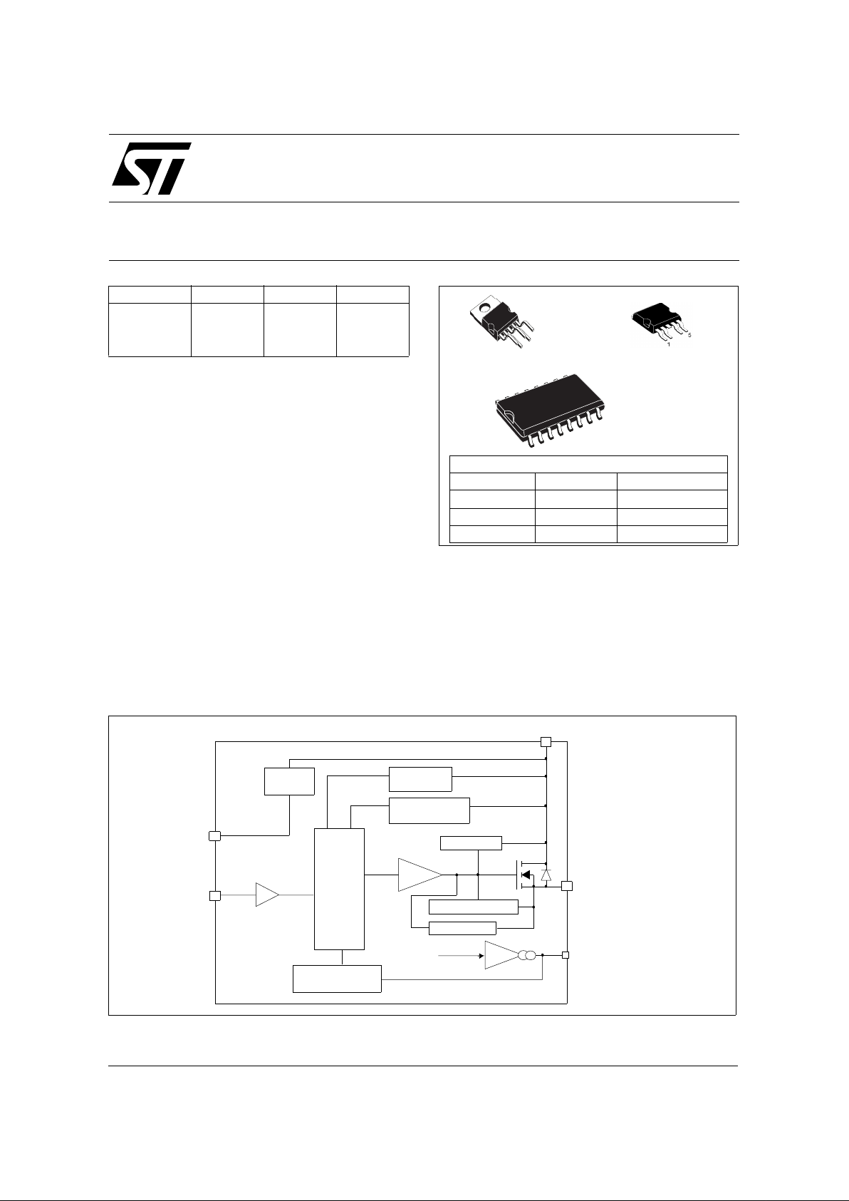
VN920
/ VN920- B5 / VN920 SO
SINGLE CHANNEL HIGH SIDE SOLID STATE RELAY
■ CMOS COMPATIBLE INPUT
■ PROPORTIONAL LOAD CURRENT SENSE
■ SHORTED LOAD PROTECTION
■ UNDERVOLTAGE AND OVERVOLTAGE
SHUTDOWN
■ OVERVOLTAGE CLAMP
■ THERMAL SHUTDOWN
■ CURRENT LIMITATION
■ PROTECTION AGAI NST LOSS OF GROUND
AND LOSS OF V
CC
■ VERY LOW ST AND -BY P OWER DI SSIPA TION
■ REVERSE BA TTERY PROTECTION (*)
DESCRIPTION
The VN920, VN920-B5, VN920SO is a monolithic
device made by using STMicroelectronics
VIPower M0-3 Technology, intended for driving
any kind of load with one side connected to
ground. Active VCC pin voltage clamp protects the
device a gainst low energy spi kes (see ISO7637
transient compatibility table). Active current
limitation combined with thermal shutdown and
automatic restart protect the device against
overload. The device integrates an analog current
sense output which delivers a current proportional
to the load cu rren t. Device a utoma ti cally turn s off
in case of ground pin disconnection.
TYPE R
DS(on)
I
OUT
V
CC
VN920
VN920-B5
VN920SO
16mΩ 30 A 36 V
PENTAWATT
P2PAK
SO-16L
ORDER CODE S
PACKAGE TUBE T&R
PENTAWATT
VN920
P2PAK VN920 -B5 VN920-B51 3TR
SO-16L V N920 SO VN920SO13TR
BLOCK DIAGRAM
(*) See application schematic at page 8
2/23
VN920 / VN920-B5 / VN920SO
ABSOLUTE MAXIMUM RATI NG
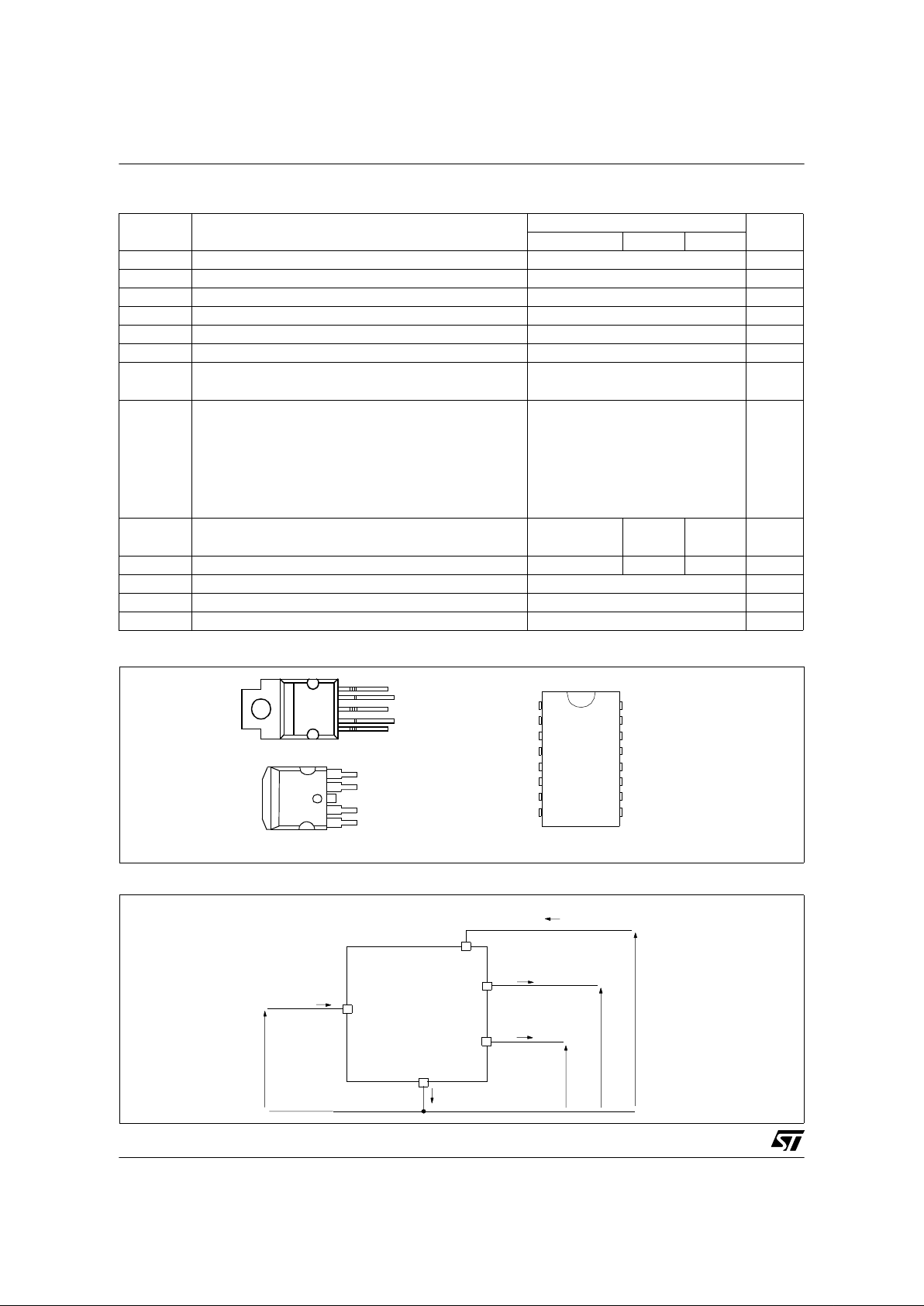
CONNECTION DIAGRAM (TOP VIEW)
CURRENT AND VOLTAGE CONVENTIONS
Symbol Parameter
Value
Unit
PENTAWATT P
2
PAK SO-16L
V
CC
DC Supply Voltage 41 V
- V
CC
Reverse DC Supply Voltage - 0.3 V
- I
GND
DC Reverse Ground Pin Current - 200 mA
I
OUT
DC Output Current Internally Limited A
- I
OUT
Reverse DC Ou tput Current - 21 A
I
IN
DC Input Current +/- 10 mA
V
CSENSE
Current Sense Maximum Voltage -3
+15
V
V
V
ESD
Electrostatic Discharge
(Human Bo dy Model: R=1.5KΩ; C=100pF)
- INPUT
- CURRENT SENSE
- OUTPUT
- V
CC
4000
2000
5000
5000
V
V
V
V
E
MAX
Maxim u m Sw itching Energy
(L=0.25m H ; R
L
=0Ω; V
bat
=13.5V ; T
jstart
=150ºC ; IL=45A)
364 352 mJ
P
TOT
Power Diss ipation TC≤25°C 96.1 96.1 8.3 W
T
j
Junction Operating Temperature Internally limited °C
T
c
Case Operating Temperature - 40 to 150 °C
T
STG
Storage Temperat ure - 55 to 150 °C
1
5
4
3
2
1
V
CC
GND
INPUT
C
SENSE
OUTPUT
PENTAWATT
3
2
1
4
5
V
CC
GND
INPUT
C
SENSE
OUTPUT
P2PAK
I
S
I
GND
V
CC
V
CC
V
SENSE
OUTPUT
I
OUT
CURRENT SENSE
I
SENSE
INPUT
I
IN
V
IN
V
OUT
GND
V
CC
OUTPUT
OUTPUT
OUTPUT
OUTPUT
V
CC
OUTPUT
OUTPUT
V
CC
N.C.
N.C.
C
SENSE
INPUT
V
CC
GND
N.C.
1
8
9
16
SO-16L
3/23
VN920 / VN920-B5 / VN920SO
THERMAL DATA
(*) When mounted on a standard single-sid ed FR-4 board with 0.5cm2 of Cu (at leas t 35µ m t hick) .
(**) When mounted on a standa r d s ingle-sided FR-4 board with 0.5cm
2
of Cu (at least 35µm thick) connected to all VCC pins.
ELECTRICAL CHARACTERISTICS (8V<VCC<36V; -40°C<Tj<150°C unless otherwise specified)
POWER
SWITCHING (VCC=13V)
LOGIC INPUT
Symbol Parameter
Value
Unit
PENTAWATT P
2
PAK SO-16L
R
thj-case
Thermal R esistance Junction- case Max 1.3 1.3 °C/W
R
thj-lead
Thermal Resistance Junction-lead Max 15 °C/W
R
thj-amb
Thermal Resistance Junction-ambient M ax 61.3 51.3 (*) 65 (**) °C/W
Symbol Parameter Test Conditions Min Typ Max Unit
V
CC
Operating Supply Voltage 5.5 13 36 V
V
USD
Undervoltage Shut-down 3 4 5.5 V
V
OV
Overvolt age Shut-down 36 V
R
ON
On State Resistance
I
OUT
=10A; Tj=25°C
I
OUT
=10A
I
OUT
=3A; VCC=6V
16
32
55
mΩ
mΩ
mΩ
V
clamp
Clam p Vo ltage ICC=20mA (See note 1) 41 48 55 V
I
S
Supply Current
Off State; V
CC
=13V; VIN=V
OUT
=0V
Off State; V
CC
=13V; VIN=V
OUT
=0V; Tj=25°C
On State; V
CC
=13V; VIN=5V; I
OUT
=0A;
R
SENSE
=3.9KΩ
10
10
25
20
5
µA
µA
mA
I
L(off1)
Off State Output Curren t VIN=V
OUT
=0V 0 50 µA
I
L(off2)
Off State Output Curren t VIN=0V; V
OUT
=3.5V -75 0 µA
I
L(off3)
Off State Output Curren t VIN=V
OUT
=0V; Vcc=13V; Tj=125°C 5 µA
I
L(off4)
Off State Output Curren t VIN=V
OUT
=0V; Vcc=13V; Tj=25°C 3 µA
Symbol Parameter Test Conditions Min Typ Max Unit
t
d(on)
Turn-on Delay Time RL=1.3Ω (s ee figure 2) 50 µs
t
d(off)
Turn-off Dela y Ti me RL=1.3Ω (see figure 2) 50 µs
dV
OUT
/dt
(on)
Turn-on Voltage Sl ope RL=1.3Ω (s ee figure 2)
See
relative
diagram
V/µs
dV
OUT
/dt
(off)
Turn-off Voltage Slope RL=1.3Ω (see figure 2)
See
relative
diagram
V/µs
Symbol Parameter Test Co nditions Min Typ Max U nit
V
IL
Input Low Level 1.25 V
I
IL
Low Level Input Current VIN=1.25V 1 µA
V
IH
Input High Level 3.25 V
I
IH
High Level Input Current VIN=3.25V 10 µA
V
I(hyst)
Input Hyst eresis Voltage 0.5 V
V
ICL
Input Clamp Voltage
I
IN
=1mA
I
IN
=-1mA
66.8
-0.7
8V
V
1
Note 1: V
clamp
and VOV are correlated. Typical difference is 5V .
4/23
VN920 / VN920-B5 / VN920SO
1
ELECTRICAL CHARACTERISTICS (continued)
CURRENT SENSE (9V≤ VCC≤16V) (See Fig. 1)
PROTECTIONS
Note 2: current sense signal delay after positive input sl ope
Note: sense pin doesn’t have to be left floating.
Symbol Parameter Test Conditions Min Typ Max Unit
K
1
I
OUT/ISENSE
I
OUT
=1A; V
SENSE
=0.5V;
T
j
= -40°C...150°C
3300 4400 6000
dK1/K1Current Se nse Ratio Drift
I
OUT
=1A; V
SENSE
=0.5V;
T
j
= -40°C...+150°C
-10 +10 %
K
2
I
OUT/ISENSE
I
OUT
=10A; V
SENSE
=4V; Tj=-40°C
T
j
=25°C... 150°C
4200
4400
4900
4900
6000
5750
dK2/K2Current Se nse Ratio Drift
I
OUT
=10A; V
SENSE
=4V;
T
j
=-40°C.. .+150°C
-8 +8 %
K
3
I
OUT/ISENSE
I
OUT
=30A; V
SENSE
=4V; Tj=-40°C
T
j
=25°C... 150°C
4200
4400
4900
4900
5500
5250
dK3/K3Current Se nse Ratio Drift
I
OUT
=30A; V
SENSE
=4V;
T
j
=-40°C.. .+150°C
-6 +6 %
I
SENSEO
Analog Sense Leakage
Current
V
CC
=6...16V; I
OUT
=0A;V
SENSE
=0V;
T
j
=-40°C.. .+150°C
010µA
V
SENSE
Max Analog Sense Output
Voltage
V
CC
=5.5V; I
OUT
=5A; R
SENSE
=10KΩ
V
CC
>8V; I
OUT
=10A; R
SENSE
=10KΩ
2
4
V
V
V
SENSEH
Sense Voltage in
Overtemperature
conditions
VCC=13V; R
SENSE
=3.9KΩ 5.5 V
R
VSENSEH
Analog Sense Output
Impedance in
Overtemperature
Condition
VCC=13V; Tj>T
TSD
; Output Open 400 Ω
t
DSENSE
Current sense delay
response
to 90% I
SENSE
(see note 2) 500 µs
Symbol Parameter Test Conditions Min Typ Max Unit
T
TSD
Shut-down Temperature 150 175 200 °C
T
R
Reset Temperature 135 °C
T
hyst
Thermal Hysteresis 7 1 5 °C
I
lim
DC Short Circuit Current
V
CC
=13V
5V<V
CC
<36V
30 45 75
75
A
A
V
demag
Turn-off Output Clamp
Voltage
I
OUT
=2A; VIN=0V; L= 6m H VCC-41 VCC-48 VCC-55 V
V
ON
Output Voltage Drop
Limitation
I
OUT
=1A; Tj=-40°C....+150°C 50 mV
5/23
VN920 / VN920-B5 / VN920SO
1
1
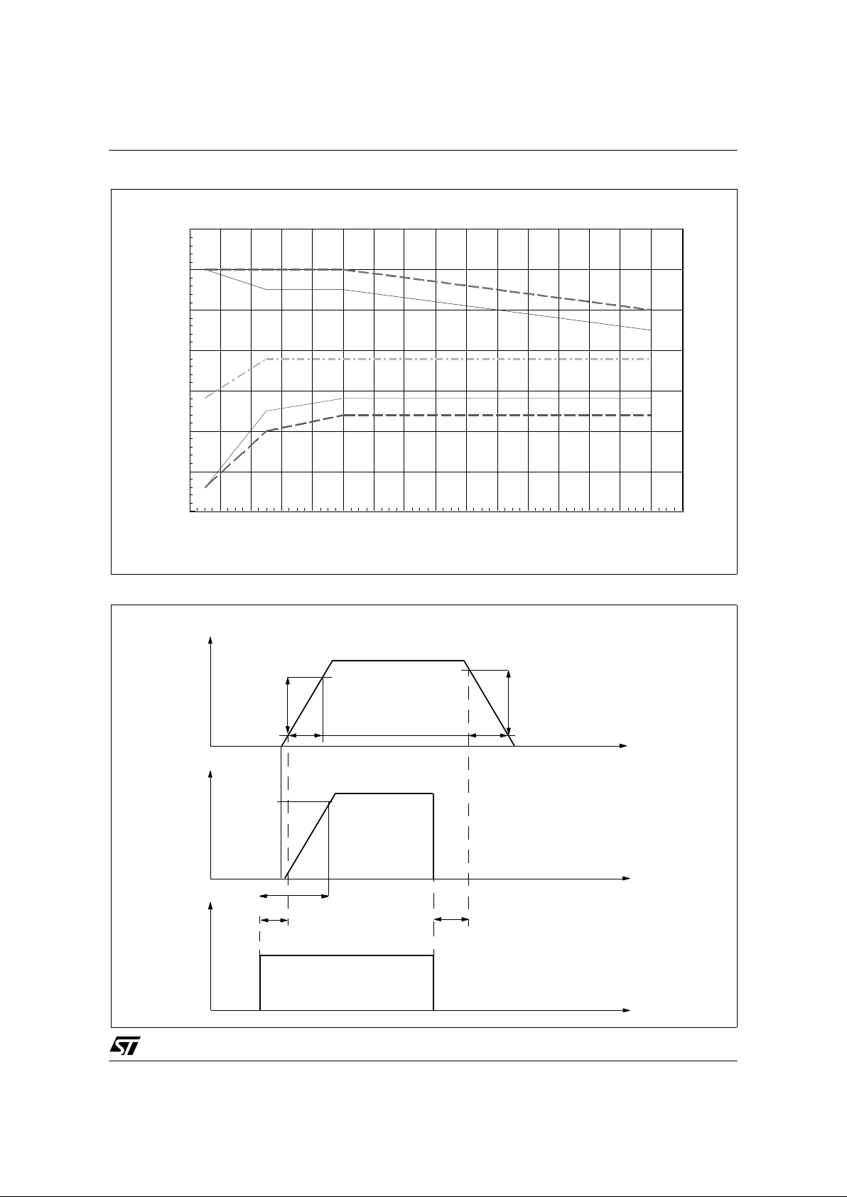
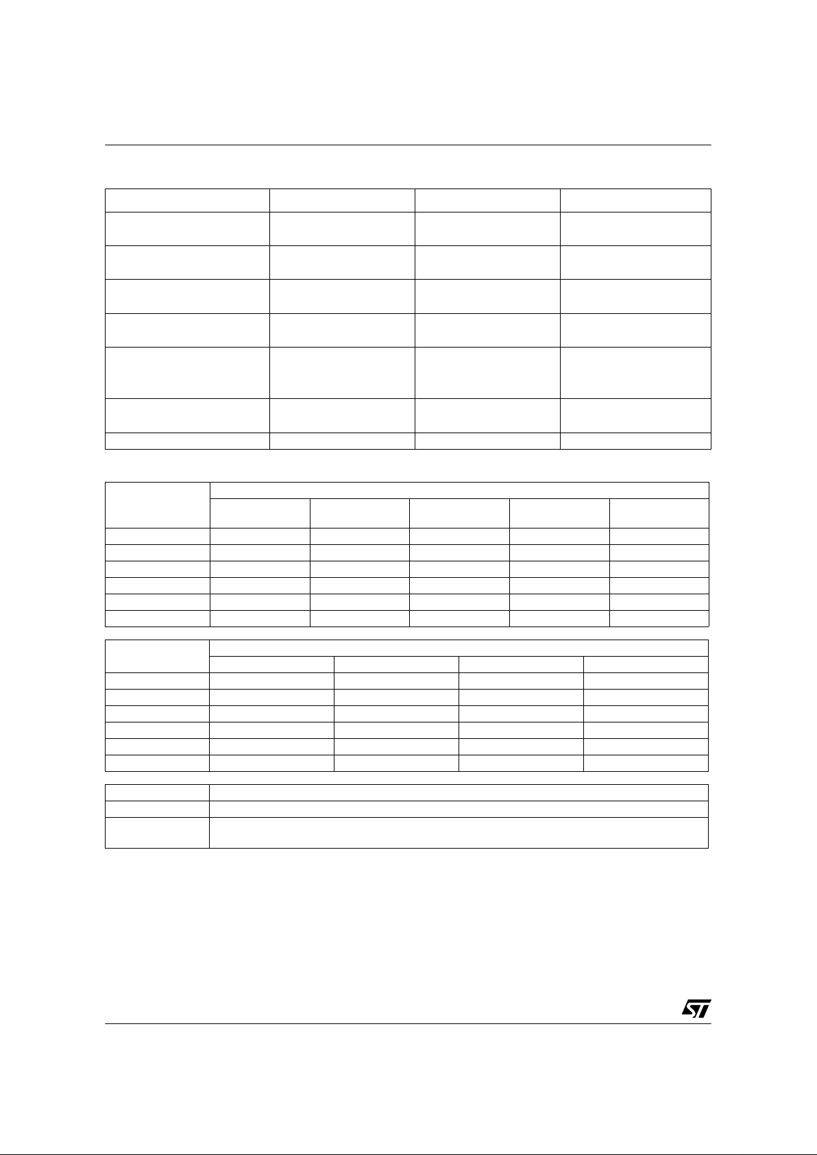
Figur e 2: Switching Characteristics (Resistive load RL=1.3Ω)
02468101214161820222426283032
3000
3500
4000
4500
5000
5500
6000
6500
min.Tj=-40°C
max.Tj=-40°C
min.Tj=25...150°C
max.Tj=25...150°C
typi cal value
Figure 1: I
OUT/ISENSE
versus I
OUT
I
OUT
(A)
I
OUT/ISENSE
V
OUT
dV
OUT
/dt
(on)
t
r
80%
10%
t
f
dV
OUT
/dt
(off)
I
SENSE
t
t
90%
t
d(off)
INPUT
t
90%
t
d(on)
t
DSENSE
6/23
VN920 / VN920-B5 / VN920SO
1
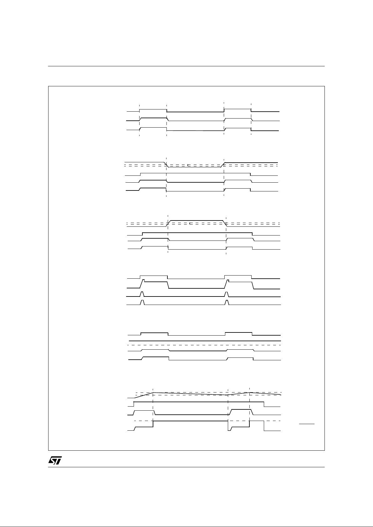
TRUTH TABLE
ELECTRICAL TRANS IENT REQUIREMENTS
CONDITIONS INPUT OUTPUT SENSE
Normal op eration
L
H
L
H
0
Nominal
Overtemperature
L
H
L
L
0
V
SENSEH
Undervoltage
L
H
L
L
0
0
Overvoltage
L
H
L
L
0
0
Short circuit to GND
L
H
H
L
L
L
0
(T
j<TTSD
) 0
(T
j>TTSD
) V
SENSEH
Short circuit to V
CC
L
H
H
H
0
< Nominal
Negative output voltage clam p L L 0
ISO T/R 7637/1
Test Pulse
TEST LEVELS
I II III IV Delays and
Impedance
1 -25 V -50 V -75 V -100 V 2 ms 10 Ω
2 +25 V +50 V +75 V +100 V 0.2 ms 10 Ω
3a -25 V -5 0 V - 100 V -150 V 0.1 µs 50 Ω
3b +25 V +50 V +75 V +100 V 0.1 µs 50 Ω
4 -4 V -5 V -6 V -7 V 100 ms, 0. 01
Ω
5 +26.5 V +46.5 V +66.5 V +86.5 V 400 ms, 2
Ω
ISO T/R 7637/1
Test Pulse
TEST LEVELS RESULTS
I II III IV
1CCCC
2CCCC
3aCCCC
3bCCCC
4CCCC
5CEEE
CLASS CONTENTS
C All functions of the device are per formed as de signed after exposure to disturbance.
E One or more functions of the device is not performed as d esigned after exposure to disturbance
and cann ot be returned to proper operation wi thout replacing the device.
7/23
VN920 / VN920-B5 / VN920SO
SENSE
INPUT
NORMAL OPERATION
UNDERVOLTAGE
V
CC
V
USD
V
USDhyst
INPUT
OVERVOLT AGE
V
CC
SENSE
INPUT
SENSE
Figure 3: W aveforms
LOAD CURRENT
LOAD CURRENT
LOAD CURREN T
OVERTEMPERATURE
INPUT
SENSE
T
TSD
T
R
T
j
LOAD CURRENT
V
OV
V
OVhyst
VCC > V
USD
SHORT TO GROUND
INPUT
LOAD CURRENT
SENSE
LOAD VOLTAGE
INPUT
LOAD VOLTAGE
SENSE
LOAD CURRENT
<Nominal
<Nominal
SHORT TO V
CC
I
SENSE
=
R
SENSE
V
SENSEH

8/23
VN920 / VN920-B5 / VN920SO
GND PROTECTION NETWORK AGAINST
REVERSE BATTERY
Soluti on 1: Resistor in the ground line (R
GND
only). This
can be us ed with any type of load.
The fo llowin g is an indica tion on how to dim ension the
R
GND
resistor.
1) R
GND
≤ 600mV / (I
S(on)ma x
).
2) R
GND
≥ (−VCC) / (-I
GND
)
where -I
GND
is the DC re vers e grou nd pi n cu rren t an d can
be found in the absolute maximum rating section of the
device’s datasheet.
Power Dissipation in R
GND
(when VCC<0: during reverse
battery situations) is:
P
D
= (-VCC)2/R
GND
This resistor can be shared amongst several different
HSD. Please note that the val u e of this resi s to r sh ou l d be
calcul ated with form ula (1) wher e I
S(on)max
becomes t he
sum of the maximum on-state currents of the different
devices.
Please note that if the microprocessor ground is not
common with the device ground then the R
GND
will
produce a shift (I
S(on)max
* R
GND
) in the input thresholds
and the status output values. This shift will vary
depend ing on how many devi ces are ON in the c ase of
several high side drivers sharing the same R
GND
.
If the calculated power dissipation leads to a large resistor
or several devices hav e to share the sa me resisto r then
the ST suggests to utiliz e Solu tio n 2 (se e below ).
Solution 2:
A diode (D
GND
) in the gr ound line.
A resistor (R
GND
=1kΩ) sh ould b e insert ed in paral lel to
D
GND
if the device will be driving an inductive load.
This small signal diode can be safely shared amongst
several different HSD. Also in this case, the presence of
the ground network wi ll produce a shift (
j
600mV) in t he
input threshold and the status output values if the
microprocessor ground is not common with the device
ground. This shift will not vary if more than one HSD
shares the same diod e/resisto r network.
LOAD DUMP PROTECTION
Dld is necessary (Voltage Transient Suppressor) if the
load dump peak voltage exceeds VCC max DC rating. The
same applies if the device will be subject to transients on
the VCC line that are grea ter tha n the ones sh own in the
ISO T/R 7637/1 table.
µ
C I/Os PROTECTION:
If a ground protection network is used and negative
transients are present on the VCC line, th e con trol p ins will
be pulled negative. ST suggests to insert a resistor (R
prot
)
in lin e to prevent the µC I/Os pins to latch-up.
The value of these resistors is a compromise between the
leakage c urrent of µC an d the current required by the
HSD I/Os ( Input le vels comp atibilit y) wi th the lat ch-up li mit
of µC I/Os.
-V
CCpeak/Ilatchup
≤ R
prot
≤ (V
OHµC-VIH-VGND
) / I
IHmax
Calculation example:
For V
CCpeak
= - 100V an d I
latchup
≥ 20mA; V
OHµC
≥ 4.5V
5kΩ ≤ R
prot
≤ 65kΩ.
Recommended R
prot
value is 10kΩ.
1
APPLICATION SCHEMATIC
V
CC
GND
OUTPUT
D
GND
R
GND
D
ld
µ
C
+5V
R
prot
V
GND
INPUT
CURRENT SENSE
R
SENSE
R
prot

9/23
VN920 / VN920-B5 / VN920SO
11
1
High Level Input Current
Input Clamp Voltage
Off State Output Current
-50 -25 0 25 50 75 100 125 150 175
Tc (°C)
0
0.5
1
1.5
2
2.5
3
3.5
4
4.5
5
Iih (uA)
Vin=3.25V
-50 -25 0 25 50 75 100 125 150 175
Tc (°C)
6
6.2
6.4
6.6
6.8
7
7.2
7.4
7.6
7.8
8
Vicl (V)
Iin=1mA
Input High Level
-50 -25 0 25 50 75 100 125 150 175
Tc (°C)
2
2.2
2.4
2.6
2.8
3
3.2
3.4
3.6
Vih (V)
Input Hysteresis VoltageInput Low Level
-50 -25 0 25 50 75 100 125 150 175
Tc (°C)
1
1.2
1.4
1.6
1.8
2
2.2
2.4
2.6
Vil (V)
-50 -25 0 25 50 75 100 125 150 175
Tc (°C)
0.5
0.6
0.7
0.8
0.9
1
1.1
1.2
1.3
1.4
1.5
Vhyst (V)
-50 -25 0 25 50 75 100 125 150 175
Tc (°C)
0
1
2
3
4
5
6
7
8
9
IL(off1) (u A)

10/23
VN920 / VN920-B5 / VN920SO
1
Overvoltage Shutdown
Turn-on Voltage Slope Turn-off Voltage Slope
I
LIM
Vs T
case
-50 -25 0 25 50 75 100 125 150 175
Tc (°C)
30
32
34
36
38
40
42
44
46
48
50
Vov (V)
-50 -25 0 25 50 75 100 125 150 175
Tc (ºC)
250
300
350
400
450
500
550
600
650
700
dVout/dt(on) (V/ms)
Vcc=13V
Rl=1.3Ohm
-50 -25 0 25 50 75 100 125 150 175
Tc (°C)
0
50
100
150
200
250
300
350
400
450
500
550
dVout/dt(off) (V/ms)
Vcc=13V
Rl=1.3Ohm
On State Resistance Vs T
case
On State Resistance Vs V
CC
-50 -25 0 25 50 75 100 125 150 175
Tc (°C)
0
10
20
30
40
50
60
70
80
90
100
Ilim (A)
Vcc=13 V
-50 -25 0 25 50 75 100 125 150 175
Tc (ºC)
0
5
10
15
20
25
30
35
40
45
50
Ron (mOhm)
Iout=10A
Vcc=8V; 36V
5 10152025303540
Vcc (V)
0
5
10
15
20
25
30
35
40
45
50
Ron (mOhm)
Tc= - 40ºC
Tc= 25ºC
Tc= 150ºC

11/23
VN920 / VN920-B5 / VN920SO
SO-16L Maximum turn off current versus load inductance
A = Single Pulse at T
Jstart
=150ºC
B= Repetitive pulse at T
Jstart
=100ºC
C= Repetitive Pulse at T
Jstart
=125ºC
Conditions:
VCC=13.5V
Values are generated with RL=0Ω
In case of repetitive pulses, T
jstart
(at beginning of each demagnetization) of every pulse must not exceed
the temperature specified above for curves B and C.
VIN, I
L
t
Demagnetization
Demagnetization
Demagnetization
1
10
100
0.01 0.1 1 10 100
L(mH)
I
LMAX (A)
A
B
C

12/23
VN920 / VN920-B5 / VN920SO
P2PAK Maximum turn off current versus load inductance
A = Single Pulse at T
Jstart
=150ºC
B= Repetitive pulse at T
Jstart
=100ºC
C= Repetitive Pulse at T
Jstart
=125ºC
Conditions:
VCC=13.5V
Values are generated with RL=0Ω
In case of repetitive pulses, T
jstart
(at beginning of each demagnetization) of every pulse must not exceed
the temperature specified above for curves B and C.
VIN, I
L
t
Demagnetization
Demagnetization
Demagnetization
1
10
100
0.01 0.1 1 10 100
L(mH)
I
LMAX (A)
A
B
C

13/23
VN920 / VN920-B5 / VN920SO
P2PAK PC Board
R
thj-amb
Vs PCB copper area in open box free air condition
P2PAK THERMAL DATA
Layout condition of Rth and Zth measurements (PCB FR4 area= 60mm x 60m m , PCB thickness=2mm,
Cu thickness=35µm, Copper areas: 0.97cm
2
, 8cm2).
30
35
40
45
50
55
0246810
PCB Cu heatsink area (cm^2)
RTHj_amb (°C/W)
Tj-Tamb=50°C

14/23
VN920 / VN920-B5 / VN920SO
1
SO-16L PC Board
R
thj-amb
Vs PCB copper area in open box free air condition
SO-16L THERMAL DATA
Layout condition of Rth and Zth measur ements (PCB FR4 area= 41m m x 48mm, PCB thickness=2mm,
Cu thickness=35µm, Copper areas: 0.5cm
2
, 6cm2).
40
45
50
55
60
65
70
01234567
PCB Cu heatsink ar ea (cm ^ 2)
RTH j-amb (°C/W)

15/23
VN920 / VN920-B5 / VN920SO
Thermal fitting model of a single channel HSD
in SO-16L
Pulse calculation formula
Thermal Parameter
Area/island (cm2)0.56
R1 (°C/W) 0.02
R2 (°C/W) 0.1
R3 ( °C/W) 2.2
R4 (°C/W) 12
R5 (°C/W) 15
R6 (°C/W) 35 20
C1 (W.s/°C) 0.0015
C2 (W.s/°C) 7.00E-03
C3 (W.s/°C) 1.50E-02
C4 (W.s/°C) 0.14
C5 (W.s/°C) 1
C6 (W.s/°C) 5 8
Z
THδ
R
TH
δ Z
THtp
1 δ–()+⋅=
where
δ tpT⁄=
SO-16L Ther mal Impedance Junction Ambient Single Puls e
0.01
0.1
1
10
100
0.0001 0.001 0.01 0.1 1 10 100 1000
Time (s)
ZTH (°C/W)
0.5 cm
2
6 cm
2
T_amb
C1
R1 R2
C2
R3
C3
R4
C4
R5
C5
R6
C6
Pd
Tj

16/23
VN920 / VN920-B5 / VN920SO
Thermal fitting model of a single channel HSD
in P2PAK
Pulse calculation formula
Thermal Parameter
Area/island (cm2)0.976
R1 (°C/W) 0.02
R2 (°C/W) 0.1
R3 ( °C/W) 0.22
R4 (°C/W) 4
R5 (°C/W) 9
R6 (°C/W) 37 22
C1 (W.s/°C) 0.0015
C2 (W.s/°C) 0.007
C3 (W.s/°C) 0.015
C4 (W.s/°C) 0.4
C5 (W.s/°C) 2
C6 (W.s/°C) 3 5
Z
THδ
R
TH
δ Z
THtp
1 δ–()+⋅=
where
δ tpT⁄=
P2PAK Thermal Impedance Junction Ambient Single Pulse
T_amb
C1
R1 R2
C2
R3
C3
R4
C4
R5
C5
R6
C6
Pd
Tj
0.01
0.1
1
10
100
1000
0.0001 0.001 0.01 0.1 1 10 100 1000
Time (s)
ZTH (°C/W)
0.97 cm
2
6 cm
2

17/23
VN920 / VN920-B5 / VN920SO
DIM.
mm. inch
MIN. TYP MAX. MIN. TYP. MAX.
A 2.65 0.104
a1 0.1 0.2 0.004 0.008
a2 2.45 0.096
b 0.35 0.49 0.014 0.019
b1 0.23 0.32 0.009 0.012
C 0.5 0.020
c1 45° (typ.)
D 10.1 10.5 0.397 0.413
E 10.0 10.65 0.393 0.419
e 1.27 0.050
e3 8.89 0.350
F 7.4 7.6 0.291 0.300
L 0.5 1.27 0.020 0.050
M 0.75 0.029
S8° (max.)
SO-16L MECHANICAL DATA

18/23
VN920 / VN920-B5 / VN920SO
DIM.
mm. inch
MIN. TYP MAX. MIN. TYP. MAX.
A 4.8 0.189
C 1.37 0.054
D 2.4 2.8 0.094 0.110
D1 1.2 1.35 0.047 0.053
E 0.35 0.55 0.014 0.022
F 0.8 1.05 0.031 0.041
F1 1 1.4 0.039 0.055
G 3.2 3.4 3.6 0.126 0.134 0.142
G1 6.6 6.8 7 0.260 0.268 0.276
H2 10.4 0.409
H3 10.05 10.4 0.396 0.409
L 17.85 0.703
L1 15.75 0.620
L2 21.4 0.843
L3 22.5 0.886
L5 2.6 3 0.102 0.118
L6 15.1 15.8 0.594 0.622
L7 6 6.6 0.236 0.260
M 4.5 0.177
M1 4 0.157
Diam. 3.65 3.85 0.144 0.152
PENTAWATT (VERTICAL) MECHANICAL DATA

19/23
VN920 / VN920-B5 / VN920SO
DIM.
mm.
MIN. TYP MAX.
A4.30 4.80
A1 2.40 2.80
A2 0.03 0.23
b0.80 1.05
c0.45 0.60
c2 1.17 1.37
D8.95 9.35
D2 8.00
E 10.00 10.40
E1 8.50
e3.20 3.60
e1 6.60 7.00
L 13.70 14.50
L2 1.25 1.40
L3 0.90 1.70
L5 1.55 2.40
R
0.40
V2 0º 8º
Package We ight 1.40 Gr (typ)
P010R
P2PAK MECHANICAL DATA

20/23
VN920 / VN920-B5 / VN920SO
SO-16L TUBE SHIPMENT (no suffix)
1
All dimensions are in mm.
Base Q.ty 50
Bulk Q.ty 1000
Tube length (± 0.5) 532
A 3.5
B 13. 8
C (± 0.1) 0.6
TAPE AND REEL SHIPMENT (suf fix “13TR”)
Base Q.ty 1000
Bulk Q.ty 1000
A (max) 330
B (min) 1.5
C (± 0.2) 13
F 20.2
G (+ 2 / -0) 16.4
N (min) 60
T (max) 22.4
TAPE DIMENSIONS
According to Electronic Industries Association
(EIA) S tanda rd 481 rev. A, Feb 1986
All dimensions are i n m m .
Tape width W 16
Tape Hole Spacing P0 (± 0.1) 4
Component Spacing P 12
Hole Diameter D (± 0.1/-0) 1.5
Hole Diameter D1 (min) 1.5
Hole Position F (± 0.05) 7.5
Compartment Depth K (max) 6.5
Hole Spacing P1 (± 0.1) 2
Top
cover
tape
End
Start
No componentsNo components Components
500mm min
500mm min
Empty components pockets
saled with cover tape.
User direction of feed
A
C
B
REEL DIMENSIONS

21/23
VN920 / VN920-B5 / VN920SO
PENTAWATT TUBE SHIPMENT (no suffix)
All dimensions are in mm.
Base Q.ty 50
Bulk Q.ty 1000
Tube length (± 0.5) 532
A 18
B 33.1
C (± 0.1) 1
C
B
A

22/23
VN920 / VN920-B5 / VN920SO
P
2
PAK TUBE SHIPMENT (no suffix)
All dimensions are in mm.
Base Q.ty 50
Bulk Q.ty 1000
Tube length (± 0.5) 532
A 18
B 33. 1
C (± 0.1) 1
TAPE AND REEL SHIPMENT (suf fix “13TR”)
All dimensions are i n m m .
Base Q.ty 1000
Bulk Q.ty 1000
A (max) 330
B (min) 1.5
C (± 0.2) 13
F 20.2
G (+ 2 / -0) 24.4
N (min) 60
T (max) 30.4
TAPE DIMENSIONS
According to Electronic Industries Association
(EIA) S tanda rd 481 rev. A, Feb 1986
All dimensions are i n m m .
Tape width W 24
Tape Hole Spacing P0 (± 0.1) 4
Component Spacing P 16
Hole Diameter D (± 0.1/-0) 1.5
Hole Diameter D1 (min) 1.5
Hole Position F (± 0.05) 11.5
Compartment Depth K (max) 6.5
Hole Spacing P1 (± 0.1) 2
Top
cover
tape
End
Start
No componentsNo components Components
500mm min
500mm min
Empty components pockets
saled with cover tape.
User direction of feed
REEL DIMENSIONS
C
B
A

23/23
VN920 / VN920-B5 / VN920SO
Information furnished is believed to be accurate and r eliable. Ho wev er, STMicroelectr onics assume s no r es ponsibility for the consequenc es
of use of such information nor for any infringement of patents or other rights of third parties which may results from its use. No license is
granted by implication or otherwise under a ny patent or patent rights of STMicroelectronics. Specif ic ations mentioned in this publication are
subject to c hange withou t notice. This publication supersed es and replace s all information previous ly s upplied. ST M icroelect r on ics products
are not authorized for use as critical components in life support devices or systems without express written approval of STMicroelectronics.
The ST logo is a trademark of ST M ic r oelectronic s
2003 STMicroelectronics - Printed in ITALY- All Rights Reserved.
STMicroelectronics GROUP OF COMPANIES
Australia - Brazil - Canada - Ch ina - Finland - Franc e - Germany - Hong K ong - India - Isra el - Italy - Japan - M alaysia -
Malta - Moro c c o - S ingapore - Spain - Sweden - Swit z er land - United Kingdom - U.S.A.
http://www.st.com
 Loading...