


VN460SP
SINGLE CHANNEL HIGH SIDE SMART
SOLID STATE RELAY
TYPE V
VN460SP VCC-55V 20 m Ω 25 A 36 V
■ OUTPUTCURRENT(CONTINUOUS):
25 A @ T
■ 5 V LOGICLEVELCOMPATIBLEINPUT
■ UNDERVOLTAGE SHUT-DOWN
■ OVERVOLTAGE SHUT-DOWN
■ THERMALSHUT-DOWN
■ OPENDRAIN DIAGNOSTIC OUTPUT
■ VERY LOW STAND-BY POWER
dema g
=25oC
C
R
DS(on)
IOUT V
CC
DISSIPATION
DESCRIPTION
The VN460SP is a monolithic device made using
SGS-THOMSON Vertical Intelligent Power
Technology, intended for driving resistive or
inductive loads with one side connected to
ground.
Built-in thermal shut-down protects the chip from
over temperature and shortcircuit.
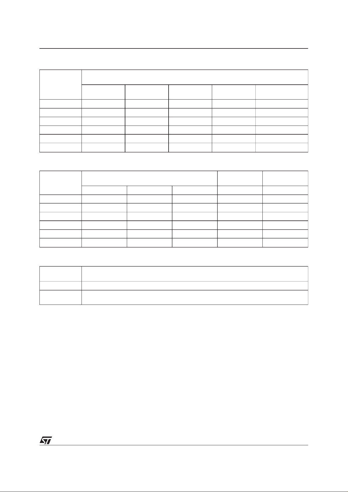
BLOCK DIAGRAM
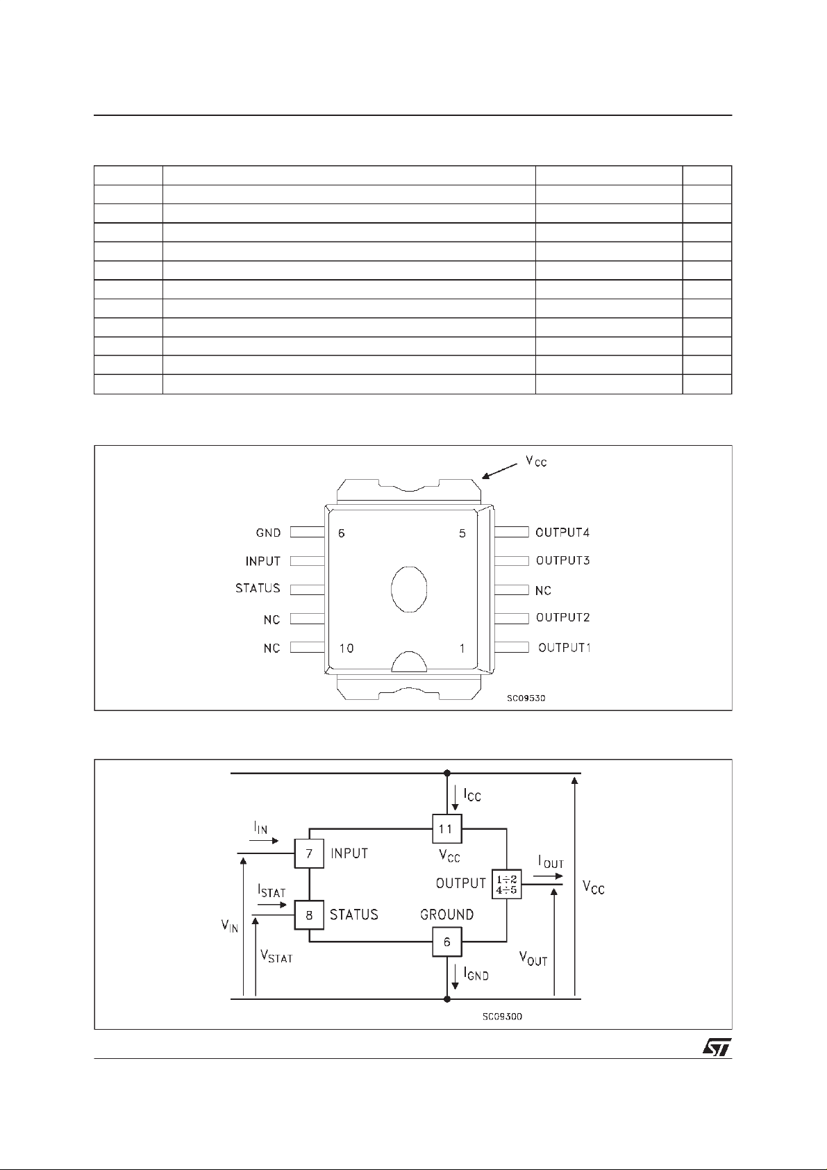
10
1
Power SO-10
TM
The control input is 5V CMOS logic level
compatible.
The open drain diagnostic output indicates open
circuit(no load) and overtemperaturestatus.
June 1998
1/9
VN460SP
ABSOLUTEMAXIMUMRATING
Symb o l Para met er Val u e Uni t
V
-V
I
OUT
I
I
I
STAT
-I
GND
V
ESD
P
T
T
CONNECTION DIAGRAM
Power Supply Voltage (continuous ) 45 V
CC
Revers e Su pply Voltage (continuous) -0. 3 V
CC
Out put Current (continuous ) Int ernally Limited A
Reverse Output Current -25 A
R
Input Current ±10 mA
IN
St at us Pin Curr ent ±10 mA
Reverse Ground Current -200 mA
Elect r o st at ic Discharge (1.5 kΩ, 100 pF ) 2000 V
Power Dissipation at Tc≤ 25oC112W
tot
Junction Operatin g Tempe rat ure -40 to 150
j
St orage Temperat ure -55 to 150
stg
o
C
o
C
CURRENT AND VOLTAGE CONVENTIONS
2/9
ELECTRICALTRANSIENTS REQUIREMENTS
VN460SP
ISO T/ R
7637/1
Test Puls e
1 -25 V -50 V -75 V -100 V 2 ms , 10 Ω
2 +2 5 V +50 V +75 V +100 V 0.2 m s , 10 Ω
3a -25 V - 50 V -100 V -150 V 0.1 µs, 50 Ω
3b +25 V +50 V +75 V +100 V 0.1 µs, 50 Ω
4 -4 V -5 V -6 V -7 V 100 ms, 0.0 1 Ω
5 +26. 5 +46. 5 +66.5 +86.5 400 ms , 2 Ω
ISO T/ R
7637/1
Test Puls e
1C C C C
2C C C C
3a C C C C
3b C C C C
4C C C C
5C E E E
(With a series resistor ≥ 1KΩin input and status pins).
I II II I IV Delays and
TEST L EVE LS RESUL TS
I II III IV
TEST LEVEL S
Impedance
CLAS S CONTENTS
C All f unction of the device ar e per f ormed as d esigne d aft er exposure to disturbanc e.
E O ne or m or e functions of the device is not per formed a s desig ned af ter exposure and
cannot be returned t o proper oper a t ion withou t r eplacing the dev ic e.
3/9
 Loading...