

SGS Thomson Microelectronics VN45013TR Datasheet
VN450
THREE CHANNELS HIGH SIDE SMART
SOLID STATE RE LAY
February 1998
Power SO-20
TM
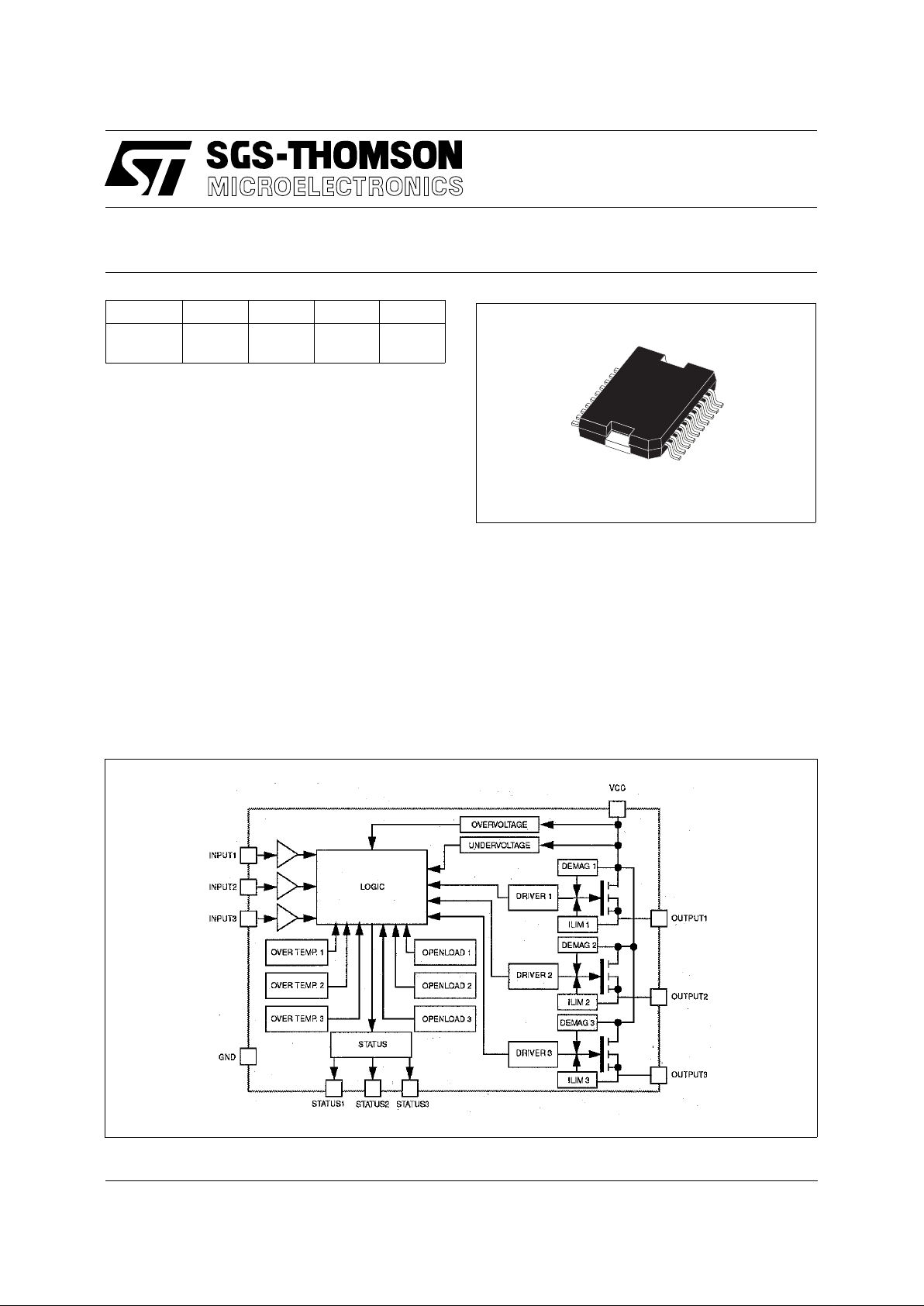
BLOCK DIAG RAM
TYPE Channel R
DS(on)
I
OUT
V
CC
VN450 1 & 2340 m Ω
300 m Ω
10 A
2 A
36 V
36 V
■ OUTPUT CURRENT (CONTINUOUS):
10 A (CHANNEL 1,2) @ T
C
= 25 o C
2 A (CHANNEL 3) @
TC = 25 o C
■ 5 V LOGIC LEVEL COMPATIBLE INPUTS
■ UNDER VOLTA G E SHUT-DO W N
■ OVER VOLTAGE SHUT-DOWN
■ THERMAL SHUT-DO WN
■ OPEN DRAIN DIAGNOSTIC OUTPUTS
■ VERY LOW STAND-BY POWER
DISSIPATION
DESCRIP TION
The VN450 is a monolithic device made using
SGS-THOMSON Vertical Intelligent Power
Technology, intended for driving resistive or
inductive loads with one side connected to
ground. This device has three independant
channels and three diagnostics.
Built-in thermal shut-down protects the chip from
over temperature and short circuit.
The control inputs are 5V CMOS logic level
compatible.
The open drain diagnostic outputs indicate short
circuit (no load) and overtemperature status.
SC09570
1/9

ABSOLUTE MAXIMUM RATING
Symbol Parameter Value Unit
V
CC
Supply Voltage (continuous) 45 V
-V
CC
Reverse Supply Voltage (continuous) -0.3 V
-I
gnd
Reverse Ground Current -200 mA
I
OUT 1,2
Output Current (continuous), channels 1, 2 10 A
I
OUT 3
Output Current (continuous), channel 3 2.5 A
I
R 1,2
Reverse Output Current (continuous) channels 1, 2 -10 A
I
R 3
Reverse Output Current (continuous) channel 3 -2.5 A
I
IN 1,2,3
Input Current ±10 mA
I
STAT 1,2,3
Status Output Current ±10 mA
V
ESD
Electrostatic Discharge (R=1.5 kΩ, C=100 pF) 2000 V
P
tot
Power Dissipation at Tc ≤ 25 oC 95 W
T
j
Junction Operating Temperature -40 to 150
o
C
T
stg
Storage Temperature -55 to 150
o
C
CONNECTION DIAGRAM
CURRENT AND VOLTAGE CONVENTI ONS
VN450
2/9

ELECTRICAL TR ANSIENTS REQUI REMENTS
ISO T/R
7637/1
Test Pulse
TEST LEVELS
I II III IV Delays and
Impedance
1 -25 V -50 V -75 V -100 V 2 ms, 10 Ω
2 +25 V +50 V +75 V +100 V 0.2 ms, 10 Ω
3a -25 V -50 V -100 V -150 V 0.1 µs, 50 Ω
3b +25 V +50 V +75 V +100 V 0.1 µs, 50 Ω
4 -4 V -5 V -6 V -7 V 100 ms, 0.01 Ω
5 +26.5 V +46.5 V +66.5 V +86.5 V 400 ms, 2 Ω
ISO T/R
7637/1
Test Pulse
TEST LEVELS RESULTS
I II III IV
1CCCC
2CCCC
3aCCCC
3bCCCC
4CCCC
5CEEE
(With a series resistor ≥ 1 KΩ in i nput and status pins).
CLASS CONTENTS
C All function of the device are performed as designed after exposure to disturbance.
E One or more functions of the device is not performed as designed after exposure and
cannot be returned to proper operation without replacing the device.
VN450
3/9
 Loading...