

SGS Thomson Microelectronics VN450 Datasheet
VN450
THREE CHANNELS HIGH SIDE SMART
SOLID STATE RELAY
TYPE Channe l R
VN450 1 & 2340 m Ω
■ OUTPUTCURRENT(CONTINUOUS):
DS(on)
300 m Ω
10 A (CHANNEL 1,2) @ T
2 A (CHANNEL 3) @T
■ 5 V LOGIC LEVELCOMPATIBLEINPUTS
■ UNDERVOLTAGE SHUT-DOWN
■ OVERVOLTAGE SHUT-DOWN
■ THERMALSHUT-DOWN
■ OPENDRAIN DIAGNOSTIC OUTPUTS
■ VERY LOW STAND-BY POWER
I
10 A
=25oC
C
=25oC
C
OUT
2A
V
CC
36 V
36 V
DISSIPATION
DESCRIPTION
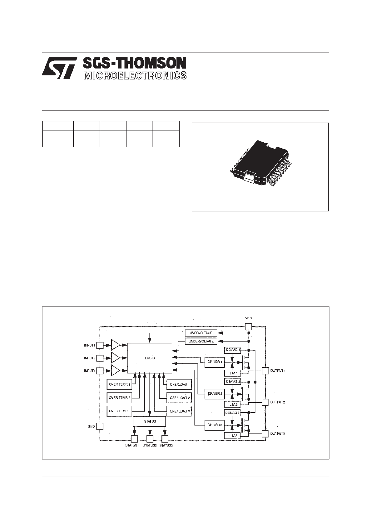
The VN450 is a monolithic device made using
SGS-THOMSON Vertical Intelligent Power
Technology, intended for driving resistive or
inductive loads with one side connected to
ground. This device has three independant
channelsand threediagnostics.
BLOCK DIAGRAM
Power SO-20
TM
Built-in thermal shut-down protects the chip from
over temperatureand short circuit.
The control inputs are 5V CMOS logic level
compatible.
The open drain diagnostic outputs indicate short
circuit(no load) and overtemperaturestatus.
February 1998
SC09570
1/9
VN450
ABSOLUTEMAXIMUMRATING
Symb o l Para met er Val u e Uni t
V
-V
-I
I
OUT 1,2
I
OUT 3
I
R1,2
I
R3
I
IN 1,2 ,3
I
STAT 1 ,2, 3
V
ESD
P
T
T
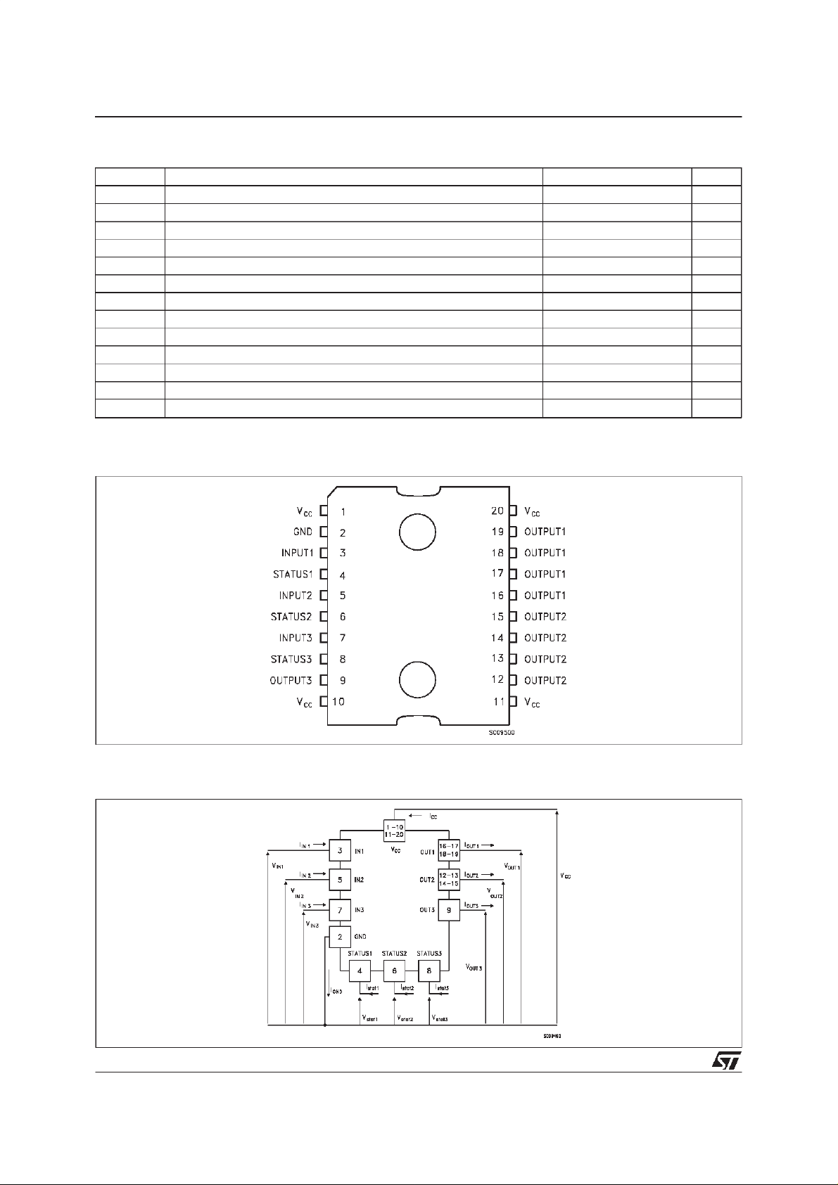
CONNECTION DIAGRAM
Supply V olt a ge ( con ti nuous ) 45 V
CC
Reverse Supply V olt ag e (cont i nuous) -0. 3 V
CC
Reverse Ground Current -200 mA
gnd
Out put Curr ent (cont inuou s) , channels 1, 2 10 A
Out put Curr ent (cont inuou s) , channel 3 2.5 A
Reverse Outp ut Current (c ontinuous) channels 1, 2 -10 A
Reverse Outp ut Current (c ontinuous) channel 3 -2. 5 A
Input Current ±10 mA
Status Output Current ±10 mA
Electrostatic Discharge (R=1.5 kΩ, C=100 pF) 2000 V
Power Dis sipation at Tc≤ 25oC95W
tot
Junct ion Opera t ing T emperature -40 t o 150
j
Sto rage T emperat ur e -55 t o 150
stg
o
C
o
C
CURRENT AND VOLTAGE CONVENTIONS
2/9
ELECTRICALTRANSIENTS REQUIREMENTS
VN450
ISO T/ R
7637/1
Test Pulse
1 -25 V -50 V -75 V -100 V 2 ms , 10 Ω
2 +2 5 V +5 0 V + 75 V +100 V 0.2 m s, 10 Ω
3a -25 V -50 V -100 V -150 V 0.1 µs, 50 Ω
3b +25 V +50 V +75 V +100 V 0.1 µs, 50 Ω
4 -4 V -5 V -6 V - 7 V 100 ms, 0.0 1 Ω
5 +26.5 V +46. 5 V + 66.5 V +86. 5 V 400 ms, 2 Ω
ISO T/ R
7637/1
Test Pulse
1CCCC
2CCCC
3aCCCC
3bCCCC
4CCCC
5CEEE
(With a series resistor ≥ 1KΩin input and status pins).
I II II I IV Delays and
IIIIIIIV
TEST LEVEL S
Impedance
TEST LEVELS RESULTS
CLAS S CONTENTS
C All f unction of the dev ice are per f ormed as designe d afte r exposur e to distu rbance.
E O ne or m or e functions of t he device is not perfor med as desig ned af ter exposure and
cannot be retu rned t o pr op er operation without replacing the device.
3/9
 Loading...