


VN410
SMART DIRECTION INDICATOR
2 CHANNEL DRIVERS
TYPE V
VN41 0 60V 4.8 A 0.07 Ω
In(✬) : ISO definition nominal current for high side automotive
switches.
■ LOADCURRENT UP TO 15A PER CHANNEL
■ OVERVOLTAGEPROTECTION
■ UNDERVOLTAGE PROTECTION
■ DOUBLE FLASHINGFREQUENCY IN LOW
DSS(cl)
In(✬ )R
on
LOADCONDITION
■ CYCLEBY CYCLEPOWERLIMITATION
■ BUZZER DRIVER
■ TRAILERINDICATION
DESCRIPTION
The VN410 is a monolithic device made using
SGS-THOMSON Vertical Intelligent Power
Technology,integrating all the featuresneeded to
implement a complete automotive flashing
system.
This device has two identical power channels, so
the informations are are specified for only one. R
pins are connected to an external R, C
C
t
networkwhich fixes the flashing frequency.LDIR,
RDIR direction inputs activate the corresponding
output (or none). EM inputs turns on both power
outputs for emergency flashing, which is reflected
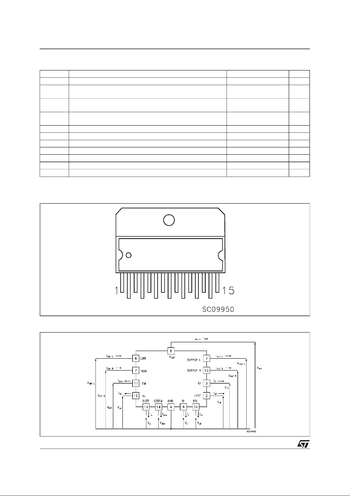
MULTIWATT-15
Order Codes :
(vertical) (In Line)
VN410 VN410(012Y)
by flashing red LED connected to LEDEM output.
AL input can be connectedto an anti-theft alarm
system, making both power outputs flashing. In
case of low load (burned lamp) buzzer frequency
and outputs flashing will double, thus indicating a
fault condition(directionmode only).
In case of overloading of the power outputs,
built-in-thermalshutdown circuits will reduce duty
,
cycle so as to keep maximum junction
t
temperature within safe limits. Rol pin is
connected to an external resistor to detect a
burned lamp and a trailer connection. LEDT is
connected to an external green LED which
indicatesthe trailerconnection.
BLOCK DIAGRAM
March 1998
1/11
VN410
ABSOLUTEMAXIMUMRATING
Symb o l Para met er Val u e Uni t
-Vbat Reverse Supply Voltage -12 V
V
BR(DSS)
V
I
I
Out
V
I
V
P
T
T
Note 1: In case the voltage drops beetween ground connection exceed 0.4V, extenal resistors in series with EM pin and AL pin areneeded
(if these pins are used)to prevent damages to the device. The value of these resistors is 100Ω.
CONNECTIONDIAGRAM
Drain-S o ur ce B reakdown V olt ag e 60
(Internally clamped)
Break dow n Voltage in Pad : LE DE M (V
p1
Break dow n Curre nt in Pad : RT , CT , R O L
p1
LDIR,RDI R
(V
bat
bat
<15V)
> 15V )
V
bat
15
+/- 10
-10/+100
Maximum DC Load Curr ent 15 A
Volt age Drop Bet we en grou nd co nnec tions (see note 1) 0.4 V
gnd
Reverse Ou tput Current -15 A
R
Electrostatic Discharge (R = 1.5 kΩ, C = 100 pF ) 2000 V
esd
Power Dissipation at Tc≤ 25oC Int ernally Li mit ed W
tot
Junction Oper at in g Temper at ure Int ernally Li mit ed
j
St orage Temperature -55 t o 150
stg
V
V
V
mA
mA
o
C
o
C
CURRENT ANDVOLTAGECONVENTIONS
2/11

ELECTRICALTRANSIENTS REQUIREMENTS
VN410
ISO T/ R
TEXT LEVEL S
7637/1
Test Pulse
I II II I IV Delays and
1 -25 V -50 V -75 V -100 V 2 ms , 10 Ω
2 +2 5 V +50 V +75 V +100 V 0.2 m s , 10 Ω
3a -25 V -50 V -100 V -150 V 100 µs, 50 Ω
3b +25 V +5 0 V +75 V +100 V 100 µs, 50 Ω
4 -4 V -5 V -6 V -7 V 100 ms , 0. 0 1 Ω
5 +26.5 + 46.5 + 6 6. 5 +86.5 400 ms, 2 Ω
ISO T/ R
TEXT LEVELS RESULTS ∗
7637/1
Test Pulse
I II III IV
1C C E E
2C C E E
3a C C C C
3b C C C C
4C C C C
5C C E E
* :with an external capacitor of 22nF connected between V
10µH output inductance.
and GND, with loads connected(2 bulbs per channel),and with a maximum of
bat
CLAS S CONTENTS
Impedance
C All f unction of the dev ic e ar e per f ormed as designed af t e r expos ure to disturbance.
E O ne or more fu nc tions of the de vice i s not perf or med as desig ned aft er exposure and
cannot be returned to pr op er operat ion without r eplacing the devic e.
3/11

VN410
THERMALDATA
R
thj-case
ELECTRICAL CHARACTERISTICS (10V < VCC<18V;-40oC<TJ< 125oC unlessotherwise
specified)
POWER
Symbol Parameter Test C ondition s Min. Typ. Max. Un it
V
R
I
SWITCHING
Symbol Parameter Test C ondition s Min. Typ. Max. Un it
(di/dt)
(di/dt)
Thermal Resistance Junction-case (1) Max 1.5
Oper at i ng Voltage 6 13 18 V
bat
On State Resis t a nc e
on
(per C hannel )
Supply Quies c ent
sq
Current
Tur n-on Current Slope R
on
Tur n-of f C urr ent Slope R
off
TC=25oCV
I
out=Inominal
TC=25oCV
bat
bat
=13V
=13V
Off State
=2.7Ω; TC=25oC; V
load
=2.7Ω; TC=25oC; V
load
=13 V 0.01 A /µ s
bat
=13 V 0.01 A /µ s
bat
0.07 Ω
100 µA
o
C/W
FLASHING
Symbol Parameter Test C ondition s Min. Typ. Max. Un it
f
δ
δ
I
dir
I
dir
I
em
I
I
dm1
I
dm2
I
I
T
T
T
I
df1
I
df2
I
Flas hing frequen c y
b
Rt= 2400
Ω
Ct=100 nF 2 4 1.6 Hz
(normal operation)
Duty C y cle Directi on Indic ator Flashing M ode 0.45
1
Duty C y cle Emergency and Alarm F lashing
2
0.35
Mode
Direction Currents R
L
=470Ω;R2= 470 Ω ;TC=25oC5 2040mA
1
R
Emer gency S ourc e
Vem=1V; TC=25oC52040mA
Current
Alarm So urce Current Val=2V; TC=25oC52040mA
al
LED Sour c e Cur rent
LEDEM pin s hort circuited to GND 35 120 mA
(emer gen c y flashing)
LED Sink Curr ent
15 70 mA
(emer gen c y flashing)
LED Curr ent ( trailer
et
LEDT pin shor t c irc u it ed t o GND 35 120 mA
indicat o r)
Buzz e r Current BUZ Z pin short cir cuited to GND 250 1000 mA
z
On Time Buzzer Rt = 3000 Ω; Ct= 100 nF 348 ms
z
Buzzer Filter Time Rt = 3 000 Ω; Ct= 1 00 n F 8 28 ms
fz
Alarm F iltering Tim e Rt = 3000 Ω; Ct= 100 nF 15 40 m s
al
Current T hreshold f or
Rol= 1 000 Ω; V
= 10 V 1.94 3.04 A
bat
Double Frequ ency
Current T hreshold f or
Rol= 1 000 Ω; V
= 18 V 2.64 4.22 A
bat
Double Frequ ency
Current T hreshold f or
t1
Rol= 1 000 Ω; V
= 10 V 3.52 4.56 A
bat
Tr ailer Det ection
4/11
 Loading...