

SGS Thomson Microelectronics VN380SP, VN380 Datasheet
VN380
TYPE V
VN38 0 60 V 5 A 0.11 Ω
VN380SP 60 V 5 A 0.11 Ω
■ LOADCURRENT UP TO 7 A
■ CMOS COMPATIBLE
■ THERMALSHUTDOWN
■ DIGNOSTICOUTPUT
■ INTEGRATEDCLAMPS
■ OVERCURRENT PROTECTION
■ OPENCOIL DETECTION
■ OVERVOLTAGEDECTION
load(c l)
I
n
R
on
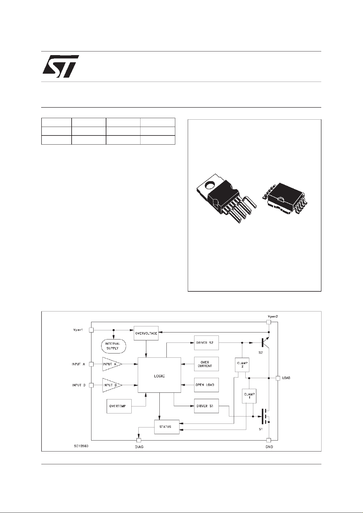
DESCRIPTION
The VN380 is a monolithic device made using
STM VIPower Technology, intended for driving
inductive loads. The inputs are CMOS
compatible. The diagnostic output provides an
indication of open load and demagnetization
mode. Built-in thermal shut-down protects the
chip from over-temperature. In case or
over-current or over-temperature or over-voltage
the product will automatically operate in
recirculationmode.
VN380SP
SMART SOLENOID DRIVER
SOLID STATE RELAY
10
1
HEPTAWATT PowerSO-1O
ORDER CODES:
HEPTAWATT VN380
PowerSO-1O VN380SP
BLOCK DIAGRAM
June 1998
1/9
VN380
ABSOLUTEMAXIMUMRATING
Symb o l Para met er Val u e Uni t
V
load
I
load
I
rload
E
E
I
I
diag
V
V
pwr1
V
pwr2
RV
T
T
V
V
diag
C
load
Note (❉) :Higher temperatureis allowed during a short time
before thermal shutdown. Permanent operation above
not allowed.
Maximum DC Load V ol t age (Internally c la m ped) V
Maximum DC Load Cur rent (Internally clamped) A
Revers e Load Current , T
Maximum Clam ping Energy , T
c
= 25oC-10A
case
= 150oC, f = 40 Hz,
case
100 mJ
1000 hou rs (f : Input A fr e quenc y)
Maximum Clam ping Energy , T
c
= -40oC,f=75Hz,
case
200 mJ
5 m inut es (f : I nput A fr eque nc y)
Input s C urr ent +/- 10 mA
in
Diagnostic O ut put Current +/- 10 mA
Electrostatic Discharge (R = 1.5 kΩ, C = 100 pF, all pins) 2000 V
esd
Power Voltage 1 60 V
Power Voltage 2 60 V
Reverse Power Voltage -0.3 V
pwr
Junction Operat ing Tempe rat ure -40 to 150 (❉)
j
St orage Tem per at ure -55 t o 150
stg
Input Volt ages 8 V
in
Diagnostic O ut put Voltag e 8 V
Load Cap acit y 1 µF
o
C 150is
o
C
o
C
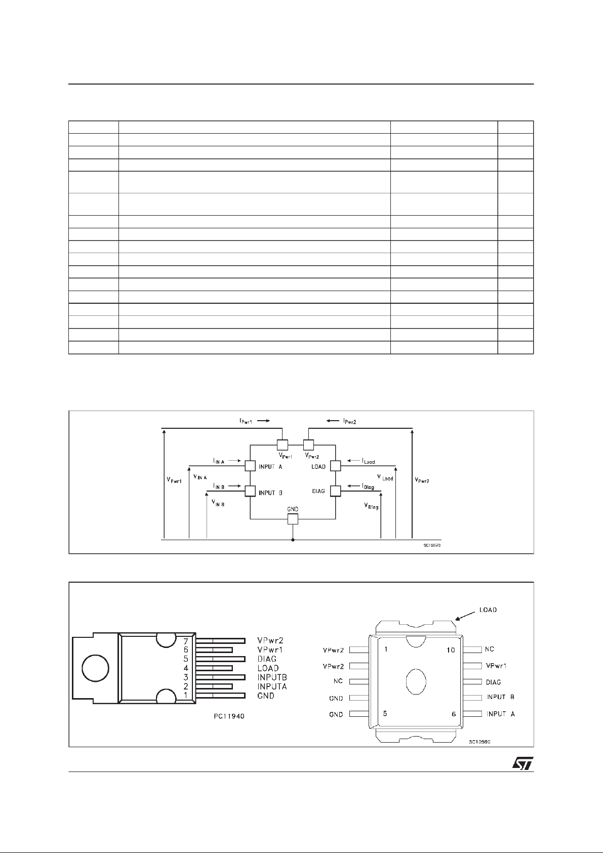
CURRENT ANDVOLTAGE CONVENTIONS
CONNECTION DIAGRAM
HEPTAWATT PowerSO-10
2/9

THERMALDATA
R
thj-case
R
thj-amb
(∗) When mounted using minimum recommended pad size on FR-4 board.
Ther mal Resist ance Junct ion-c ase Max 1.8 1.67
Ther mal Resist ance Junct ion-am b ient (∗) Max 60 50
HEPTAWATT PowerSO-10
VN380
o
C/W
o
C/W
ELECTRICAL CHARACTERISTICS (10V < V
<18V;- 40oC<TJ< 150oC unless otherwise
PWR1
specified)
POWER
Symbol Parameter Test Conditions Min. Typ. Max. Unit
V
R
R
V
ce(sat)
pwr1
I
Oper at i ng V o lt age 6 13 24 V
On S t ate Resist ance
on1
(exc it a t ion pat h )
On S t ate Resist ance
on2
(reci rc ula t ion path)
Saturation Voltage of
Bipolar S2
Supply Quiesc ent
sq
I
load=In
V
inA=VinB
V
pwr1
V
inA
=5A
=5V
=13V I
=5V V
load=In
Iload = In=5A
V
pwr1=Vpwr2
I
=10A TJ>125oC
load
V
pwr1=Vpwr2
V
=13V V
pwr1
=13V
=13V
=GND
inB
inA=VinB
=5A
=5V 25 mA
0.2 Ω
0.4 Ω
2
2
Current
I
Out put Le ak age
lk
V
=18V V
pwr1
inA=VinB
=GND 5 mA
Current
I
Off State Supply
off
Current
V
inA=VinB
V
= Not Conn ected
pwr1
10V<V
T
=25oC
J
pwr2
=GND
<24V
50 µA
SWITCHING(EXCITATION PATH)
V
V
Symbol Parameter Test Conditions Min. Typ. Max. Unit
t
d(on)
Turn-on D elay Time R
t
Rise Time o f Output
r
load
R
load
=2.5Ω V
=2.5
Ω
= 5 V (see fig.1) 50 µs
inA
V
= 5 V (see fig.1 ) 1 20 µs
inA
Current
t
d(off)
Turn-off Delay T ime R
t
Fall Time of O ut put
f
load
R
load
=2.5
Ω
=2.5Ω V
V
= 5 V (see fig.1 ) 50 µs
inA
= 5 V (see fig.1) 1 20 µs
inA
Current
LOGIC INPUT
Symbol Parameter Test Conditions Min. Typ. Max. Unit
V
V
i(hyst)
V
V
i(CL)
I
Input Low Level
il
Volt age
Input Hig h Lev el
ih
3.5 V
Volt age
Input hysteresis
0.5 0.8 2 V
Volt age
Input Cla m p Volt ag e Iin = 10 m A 8 9.5 11 V
Input Current VinA = V
in
V
inA=VinB
inB
=2V
=5V
20
1.5 V
250
µA
µA
3/9
 Loading...