

VN31SP
HIGH SIDE SMART POWER SOLID STATE RELAY
TYPE V
VN31SP 60 V 0.03 Ω 11.5 A 26 V
■ MAXIMUMCONTINUOUS OUTPUT
DSS
CURRENT(#):31 A @T
■ 5 V LOGICLEVELCOMPATIBLEINPUT
■ THERMALSHUT-DOWN
■ UNDER VOLTAGE PROTECTION
■ OPEN DRAIN DIAGNOSTIC OUTPUT
■ INDUCTIVELOAD FAST
R
DS(on)
=85oC
c
I
n(*)
V
CC
DEMAGNETIZATION
■ VERY LOW STAND-BYPOWER
DISSIPATION
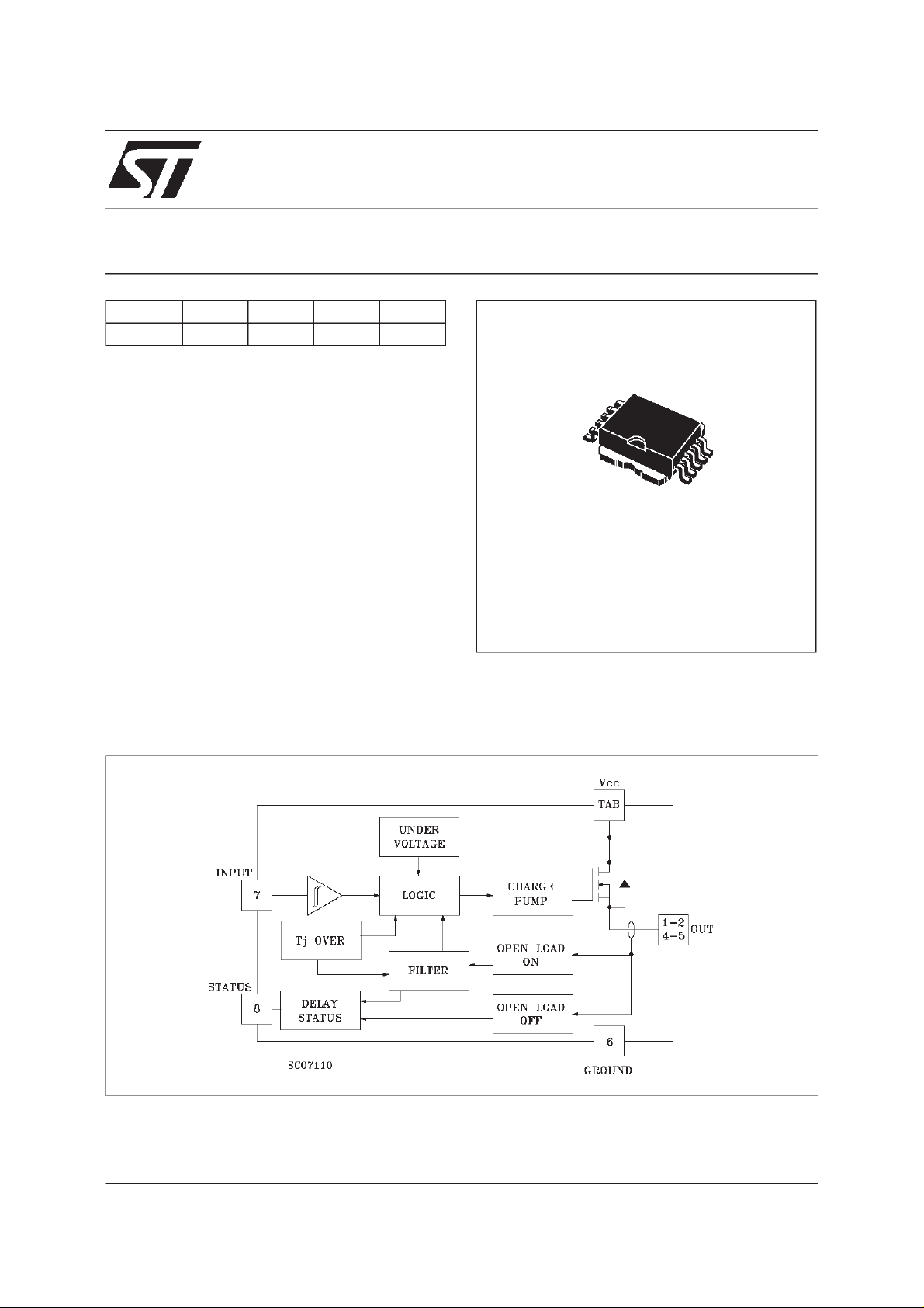
DESCRIPTION
The VN31SP is a monolithic device made using
STMicroelectronics VIPower Technology,
intended for driving resistive or inductive loads
with one side grounded.
Built-in thermal shut-down protects the chip from
over temperatureand short circuit.
The open drain diagnostic output indicates: open
load in off state, and inon state, output shorted to
BLOCK DIAGRAM
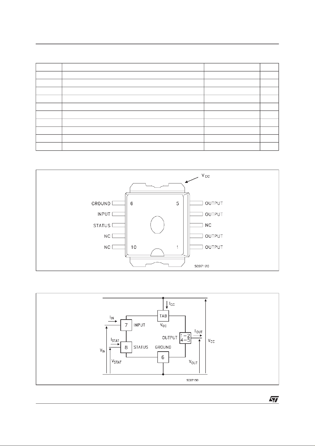
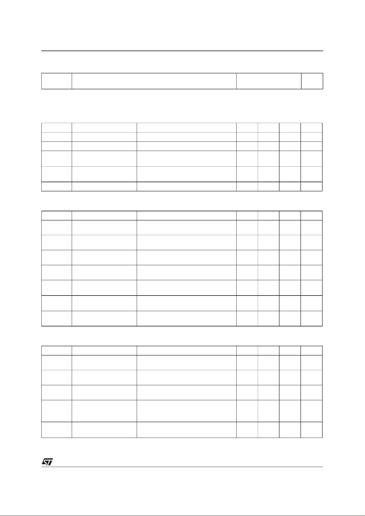
10
1
PowerSO-10
V
and overtemperature. Fast demagnetization
CC
of inductive loads is archivied by negative (-18V)
load voltageat turn-off.
(*) In = Nominal current according to ISO definition for high side automotive switch (seenote 1)
(#) The maximum continuous output current is the the current at T
protection.
July 1998
=85oC for a battery voltage of 13V whichdoes not activateself
c
1/9
VN31SP
ABSOLUTEMAXIMUMRATING
Symb o l Para met er Val u e Uni t
V
(BR)DSS
I
OUT
I
I
-V
I
STAT
V
ESD
P
T
T
CONNECTIONDIAGRAMS
Drain-S o ur ce Breakdown V olt ag e 60 V
Out put Cu rrent (cont. ) a t Tc=85oC31A
Revers e Out put Current at Tc=85oC-31A
R
Input Cur ren t ±10 mA
IN
Reverse Supply Voltage -4 V
CC
St at us Current ±10 mA
Elect r o st at ic Dis charge (1. 5 kΩ, 100 pF) 2000 V
Power Dissipation at Tc=85oC54W
tot
Junction Oper ating Tempe r at ure -40 to 150
j
St orage Tem per atur e -55 to 150
stg
o
C
o
C
CURRENT AND VOLTAGE CONVENTIONS
2/9
VN31SP
THERMALDATA
R
thj-case
R
thj- amb
($) When mounted using minimum recommended pad size on FR-4board
ELECTRICAL CHARACTERISTICS (VCC=13 V; -40 ≤ Tj≤ 125oC unlessotherwisespecified)
POWER
Symbol Parameter Test C ondition s Min. Typ. Max. Unit
V
In(*) Nominal Current T
R
I
V
DS(MAX)
SWITCHING
Symbol Parameter Test C ondition s Min. Typ. Max. Unit
t
d(on)
t
r
t
d(off)
t
f
(di/dt)
(di/dt)
V
demag
Ther mal Resistan ce Junct io n- case Max
Ther mal Resistan ce Junct io n- ambient ($ ) Max
Supply Voltag e 5.5 13 26 V
CC
=85oCV
c
On St ate Re sist ance I
on
Supply C ur rent Of f State Tj≥ 25oC
S
= 11.5 A
OUT
I
= 11.5 A Tj=25oC
OUT
≤ 0.5 (note 1) 11.5 A
DS(on)
1.2
50
On State
Maximum Voltage Drop I
(^) Tur n-on D elay T im e O f
Out put Cu rrent
(^) Rise Time Of Outp ut
Current
(^) Tur n-of f D elay Tim e Of
Out put Cu rrent
(^) Fall Time Of Output
Current
Tur n-on C ur rent S lope I
on
Tur n-of f Curr ent S lope I
off
Induc t i ve Load Clam p
=25A Tc=85oC1.5V
OUT
I
= 11.5 A Resis tive Load
OUT
90 µs
Input Ris e Time < 0.1 µs
I
= 11.5A Res is t iv e Load
OUT
100 µs
Input Ris e Time < 0.1 µs
I
= 11.5 A Resis tive Load
OUT
140 µs
Input Ris e Time < 0.1 µs
I
= 11.5 A Resis tive Load
OUT
50 µs
Input Ris e Time < 0.1 µs
= 11.5 A
OUT
I
OUT=IOV
= 11.5 A
OUT
I
OUT=IOV
I
= 11.5 A L = 1 mH -24 -18 -14 V
OUT
0.08 0.51A/µs
0.2 3
Volt age
0.06
0.03
50
15
3
o
C/W
o
C/W
Ω
Ω
µA
mA
A/µs
A/µs
A/µs
LOGIC INPUT
Symbol Parameter Test C ondition s Min. Typ. Max. Unit
V
V
V
I(hyst.)
I
V
Input Low Level
IL
Volt age
Input Hig h Level
IH
Volt age
Input Hysteresis
Volt age
Input Cur ren t VIN=5V
IN
Input Cla mp Volt ag e IIN=10mA
ICL
=2V
V
IN
=0.8V 25
V
IN
=-10mA
I
IN
0.8 V
2(•)V
0.5 V
250 500
250
5.5 6
-0.7 -0.3
µA
µA
µA
V
V
3/9
 Loading...