


VN30N
HIGH SIDE SMART POWER SOLID STATE RELAY
PRELIMINARY DATA
TYPE V
VN30N 60 V 0.03 Ω 45 A 26 V
■ OUTPUT CURRENT (CONTINUOUS): 45A @
DSS
R
DS(on)
I
OUT
V
CC
Tc=25oC
■ 5V LOGIC LEVEL COMPATIBLE INPUT
■ THERMAL SHUT-DOWN
■ UNDER VOLTAGE SHUT-DOWN
■ OPEN DRAIN DIAGNOSTIC OUTPUT
■ VERY LOW STAND-BYPOWER
DISSIPATION
DESCRIPTION
The VN30N is a monolithic device made using
SGS-THOMSON Vertical Intelligent Power
Technology, intended for driving resistive or
inductive loads with one side grounded.
Built-in thermal shut-down protects the chip from
over temperature and short circuit.
The input control is 5V logic level compatible.
The open drain diagnostic output indicates open
circuit (no load) and over temperature status.
BLOCK DIAGRAM
PENTAWATT
(vertical)
PENTAWATT
(horizontal)
PENTAWATT
(in-line)
ORDER CODES:
PENTAWATT vertical VN30N
PENTAWATT horizontal VN30N (011Y)
PENTAWATT in-line VN30N (012Y)
September 1994
1/10
VN30N
ABSOLUTE MAXIMUM RATING
Symbol Parameter Value Uni t
V
(BR)DSS
I
OUT
I
I
-V
I
STAT
V
ESD
P
T
T
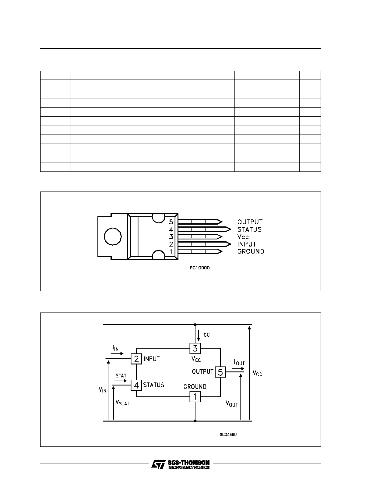
CONNECTION DIAGRAM
Drain - So urc e Br e ak down Voltage 60 V
Out put Curr ent (co nt . ) 45 A
Reverse Output Cu r r ent -45 A
R
Input Curre nt ±10 mA
IN
Reverse Supply Volt age -4 V
CC
St at us Current ±10 mA
Electrost atic Discharge (1. 5 kΩ , 100 pF ) 2000 V
Powe r Dissipatio n at Tc≤ 25oC108W
tot
Junction Op er at ing Temperat ur e -40 to 150
j
St or a ge Te mperat ur e -55 to 150
stg
o
C
o
C
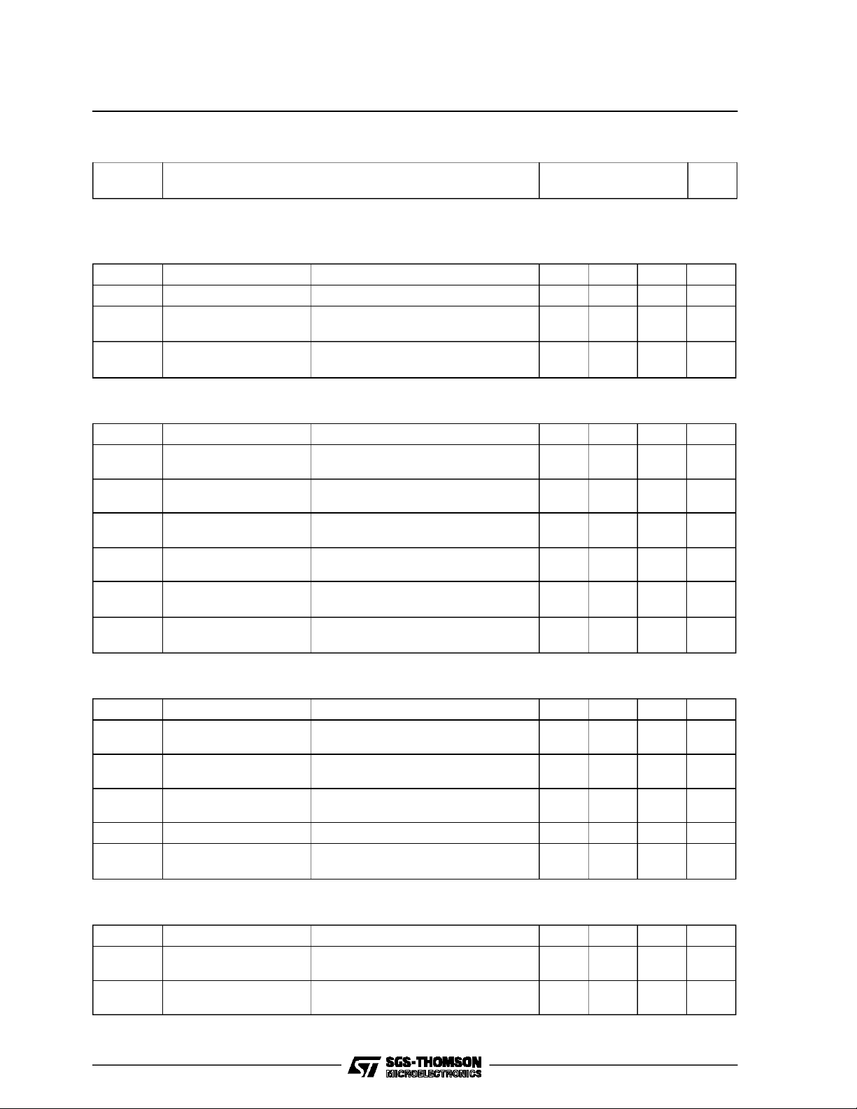
CURRENT AND VOLTAGE CONVENTIONS
2/10
VN30N
THERMAL DATA
R
thj-case
R
thj-amb
ELECTRICAL CHARACTERISTICS (VCC= 13 V; -40 ≤ Tj≤ 125oC unless otherwise specified)
POWER
Symbol Parameter Test Condition s Min. Typ. Max. Unit
V
R
I
SWITCHING
Symbol Parameter Test Condition s Min. Typ. Max. Unit
t
d(on)
t
d(off)
(di/dt)
(di/dt)
Thermal Resistance Junction-c as e Max
Thermal Resist anc e Junc t ion-ambient Max
Supply Volta ge 7 26 V
CC
On State Resistance I
on
Supply Curr ent Of f S ta te Tj≥ 25oC
S
=18A
OUT
I
=18A Tj=25oC
OUT
1.15
60
On St ate
Turn-on D elay Time Of
Out put Curr ent
Rise Time Of Output
t
r
Current
Tur n - of f Delay Time Of
Out put Curr ent
t
Fall Time Of Output
f
Current
Turn-on C urrent S lope I
on
Turn-off Current Slope I
off
I
= 18 A Resistive Load
OUT
Input Rise Time < 0.1µsT
I
= 18 A Resistive Load
OUT
=25oC
j
Input Rise Time < 0.1µsTj=25oC
I
= 18 A Resistive Load
OUT
Input Rise Time < 0.1µsTj=25oC
I
= 18 A Resistive Load
OUT
Input Rise Time < 0.1µsTj=25oC
=18A
OUT
I
OUT=IOV
=18A
OUT
I
OUT=IOV
30 µs
100 µs
80 µs
40 µs
0.06
0.03
50
15
0.53A/µs
3
4
o
C/W
o
C/W
Ω
Ω
µA
mA
A/µs
A/µs
A/µs
LOGIC INPUT
Symbol Parameter Test Condition s Min. Typ. Max. Unit
V
Input LowLevel
IL
0.8 V
Volt age
V
Input High Level
IH
2(*)V
Volt age
V
I(hyst.)
Input Hys teresis
0.5 V
Volt age
I
V
Input Curre nt VIN= 5 V 250 500 µ A
IN
Input Clamp Voltage IIN=10mA
ICL
IIN=-10mA
6
-0.7
PROTECTIONS AND DIAGNOSTICS
Symbol Parameter Test Condition s Min. Typ. Max. Unit
(•) Status V oltage Outp ut
V
STAT
Low
V
USD
Under Voltage Shut
Down
I
=1.6mA 0.4 V
STAT
6.5 7 V
V
V
3/10
 Loading...